Page 1
Fabrication and Characterization of Gecko-inspired Fibrillar Adhesive
By
Yongkwan Kim
A dissertation submitted in partial satisfaction of the
requirements for the degree of
Doctor of Philosophy
in
Chemical Engineering
in the
Graduate Division
of the
University of California, Berkeley
Committee in charge:
Professor Roya Maboudian
Professor David Graves
Professor Ali Javey
Spring 2014
Page 2
Fabrication and Characterization of Gecko-inspired Fibrillar Adhesive
Copyright 2014
by
Yongkwan Kim
Page 3
1
Abstract
Fabrication and Characterization of Gecko-inspired Fibrillar Adhesive
by
Yongkwan Kim
Doctor of Philosophy in Chemical and Biomolecular Engineering
University of California, Berkeley
Professor Roya Maboudian, Chair
Over the last decade, geckos’ remarkable ability to stick to and climb surfaces found in nature has
motivated a wide range of scientific interest in engineering gecko-mimetic surface for various
adhesive and high friction applications. The high adhesion and friction of its pads have been
attributed to a complex array of hairy structures, which maximize surface area for van der Waals
interaction between the toes and the counter-surface. While advances in micro- and
nanolithography technique have allowed fabrication of increasingly sophisticated gecko mimetic
surfaces, it remains a challenge to produce an adhesive as robust as that of the natural gecko pads.
In order to rationally design gecko adhesives, understanding the contact behavior of fibrillar
interface is critical.
The first chapter of the dissertation introduces gecko adhesion and its potential applications,
followed by a brief survey of gecko-inspired adhesives. Challenges that limit the performance of
the current adhesives are presented. In particular, it is pointed out that almost all testing of gecko
adhesives have been on clean, smooth glass, which is ideal for adhesion due to high surface energy
and low roughness. Surfaces in application are more difficult to stick to, so the understanding of
failure modes in low energy and rough surfaces is important.
The second chapter presents a fabrication method for thermoplastic gecko adhesive to be used
for a detailed study of fibrillar interfaces. Low-density polyethylene nanofibers are replicated from
a silicon nanowire array fabricated by colloidal lithography and metal-catalyzed chemical etching.
This process yields a highly ordered array of nanofibers over a large area with control over fiber
diameter, length, and number density. The high yield and consistency of the process make it ideal
for a systematic study on factors that affect adhesion and friction of gecko adhesives.
The following three chapters examine parameters that affect macroscale friction of fibrillar
adhesives. Basic geometric factors, namely fiber length and diameter, are optimized on smooth
glass for high friction. The test surfaces are then processed to intentionally introduce roughness or
lower the surface energy in a systematic and quantifiable manner, so that the failure mechanisms
Page 4
2
of the adhesive can be investigated in detail. In these studies, observed macroscale friction is
related to the nano-scale contact behavior with simple mechanical models to establish criteria to
ensure high performance of fibrillar adhesives.
Chapter 6 presents various methods to produce more complex fiber structures. The metal-
assisted chemical etching of silicon nanowires is studied in detail, where the chemical composition
of the etching bath can be varied to produce clumped, tapered, tilted, and curved nanowires, which
provide interesting templates for molding and are potentially useful for applications in various
silicon nanowire devices. Hierarchical fiber structures are fabricated by a few different methods,
as well as composite structures where the fibers are embedded in another material. A way to
precisely control tapering of microfibers is demonstrated, and the effect of tapering on macroscale
friction is studied in detail. The final chapter summarizes the dissertation and suggests possible
future works for both further investigating fibrillar interfaces and improving the current gecko
adhesive.
Page 5
i
Contents
1 Introduction to gecko-inspired synthetic adhesive 1
1.1 Gecko adhesion …………………………………………………………………… 1
1.2 Potential applications of synthetic gecko adhesive ………………………………… 3
1.3 Survey of current synthetic gecko adhesives ………………………………………. 4
1.4 Current challenges of GSAs ……………………………………………………… 6
1.5 Outline of work presented ………………………………………………………….. 7
2 Template fabrication and friction test setup 8
2.1 Fabrication process overview ……………………………………………………… 8
2.2 Colloidal lithography ……………………………. ………………………………… 9
2.3 Metal-catalyzed electroless etching of silcon template ……………………………. 11
2.4 Nanostructure molding ..…………………………………………………………… 13
2.5 Friction testing setup .….…………………………………………………………. 14
3 Effect of fiber length and diameter on macroscale friction 17
3.1 Background ……………………………………………………………………… 17
3.2 Fabricated LDPE fiber arrays …………………..………………………………… 18
3.3 Fiber clumping …………………………...………………………………………. 18
3.4 Macroscale friction of LDPE nanofiber arrays …………………………………… 19
3.5 Apparent contact area …………………………………………………………….. 22
3.6 Friction prediction and dependence on fiber diameter from JKR model …….…… 23
3.7 Friction dependence on fiber length ………………………………………………. 25
3.8 Optimum fiber length ……………………………………………………………... 28
3.9 Optimum fiber diameter …………………………………………………………... 28
3.10 Comparison with theoretical friction design map ………………………………… 29
3.11 Summary ………………………………………………………………………….. 33
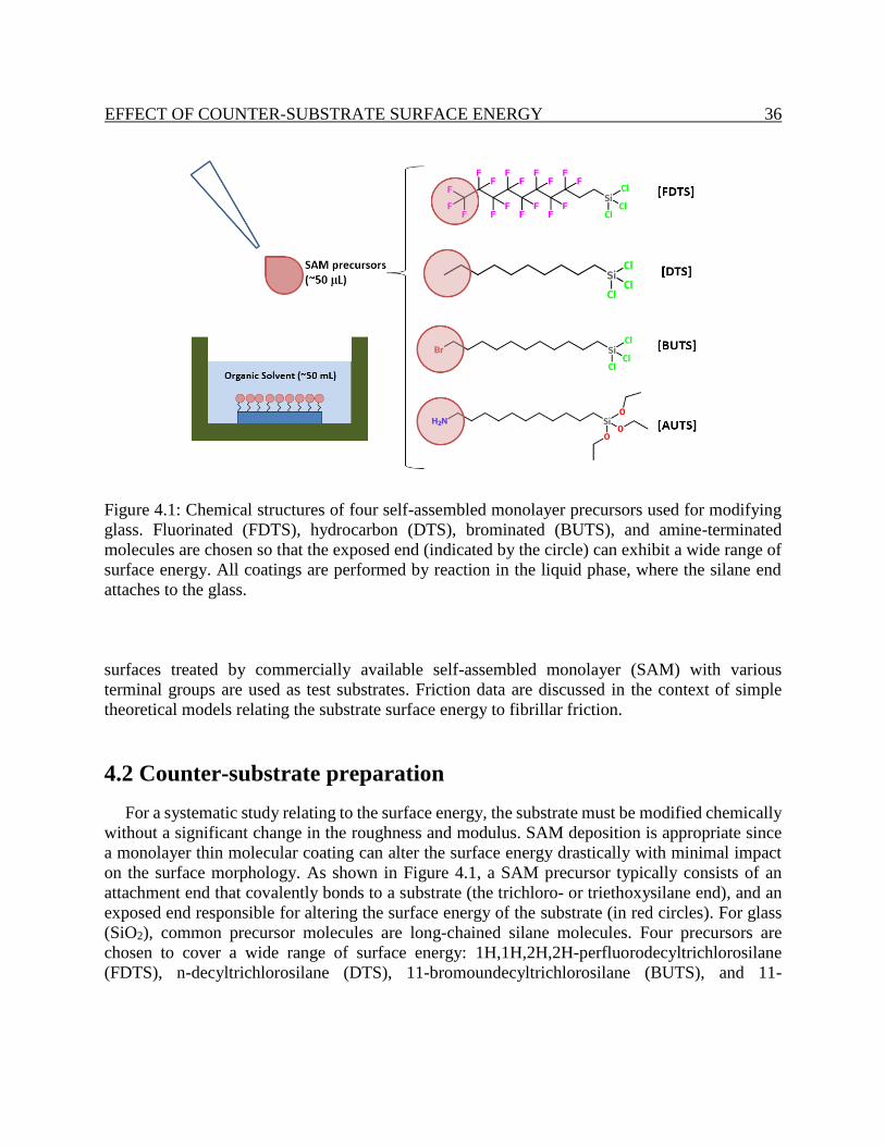
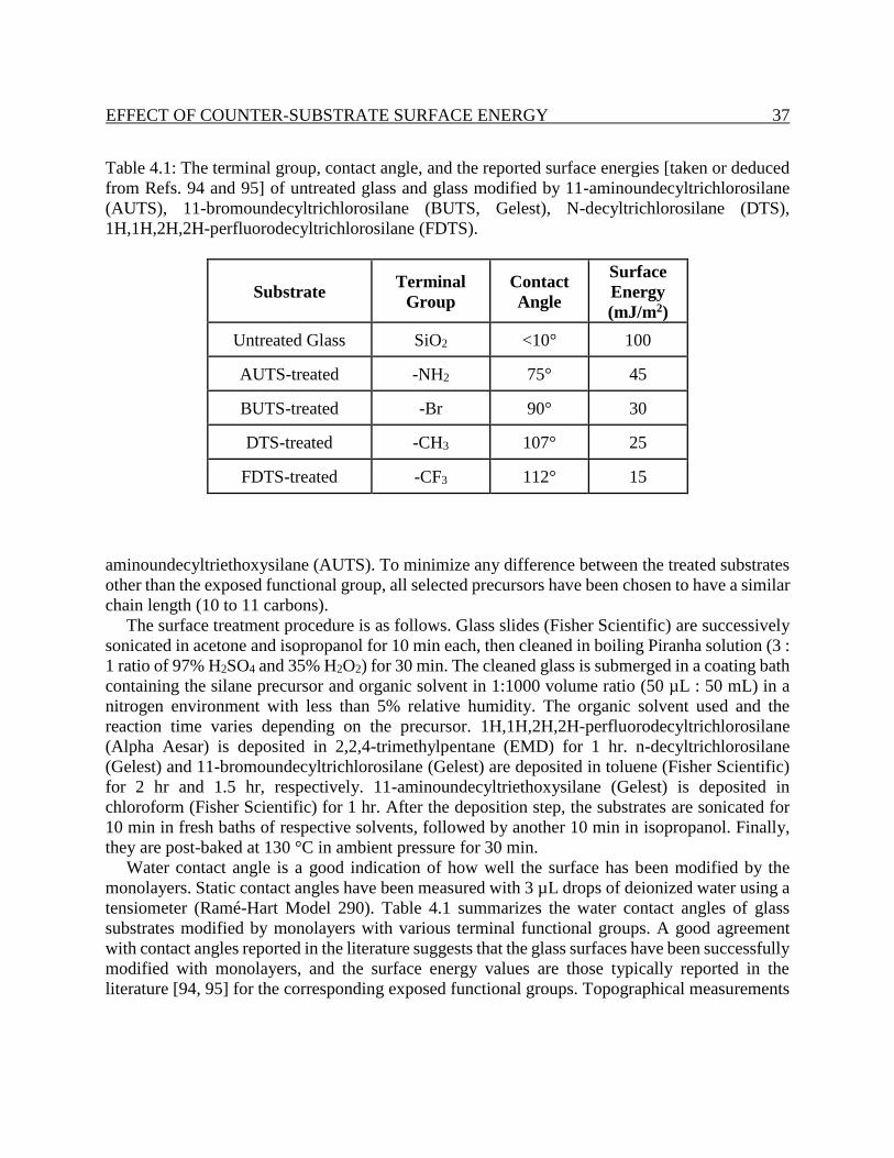
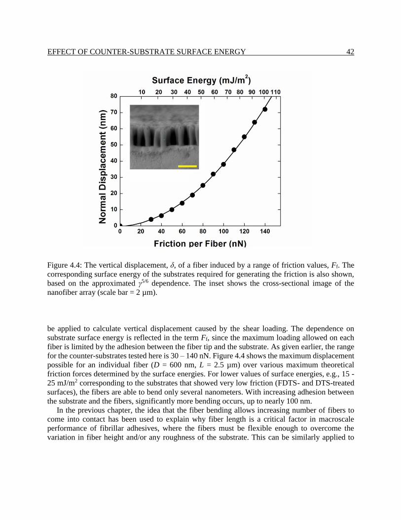
4 Effect of counter-substrate surface energy 34
4.1 Background …...……………………………………………………………...…… 34
4.2 Counter-substrate preparation …………………..………………………………… 35
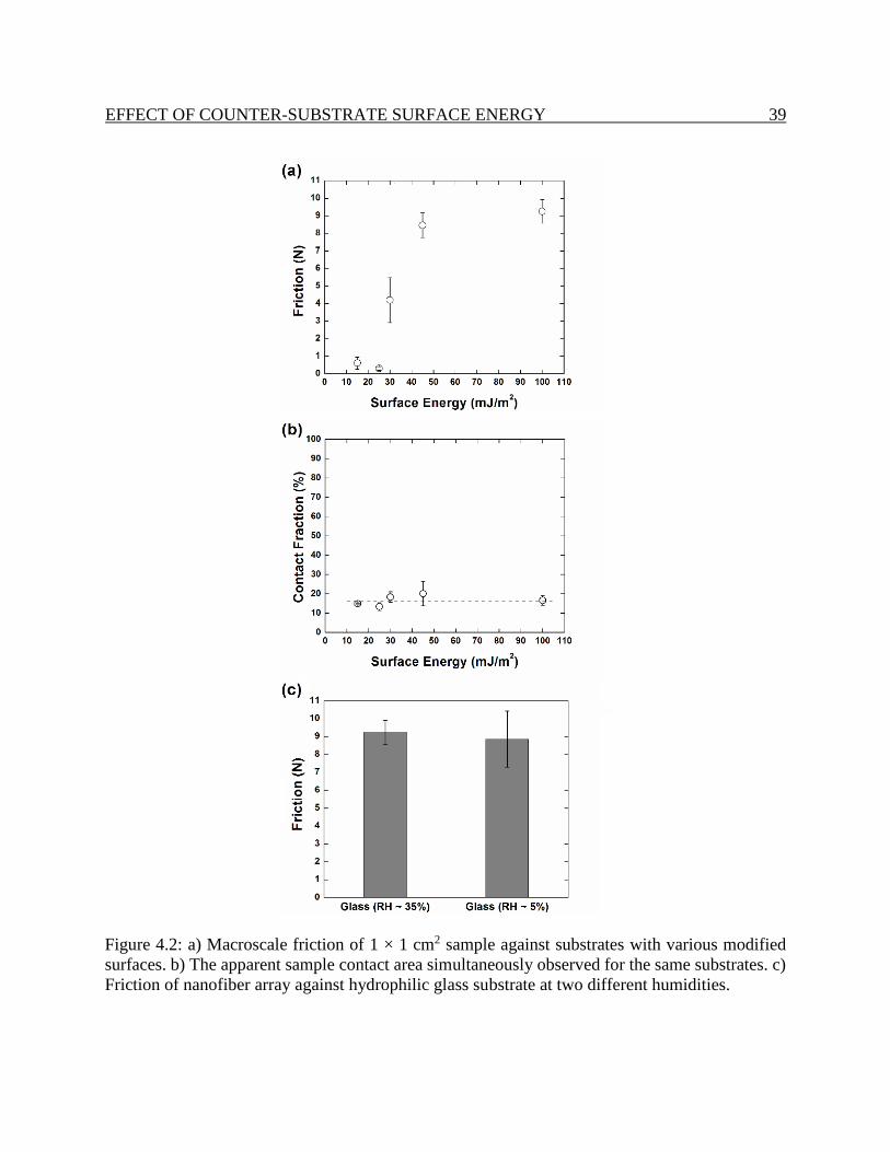
4.3 Friction and surface energy of counter-substrate …………………………………. 37
4.4 Summary ...………………..……………………………………………………… 42
5 Effect of counter-substrate roughness 44
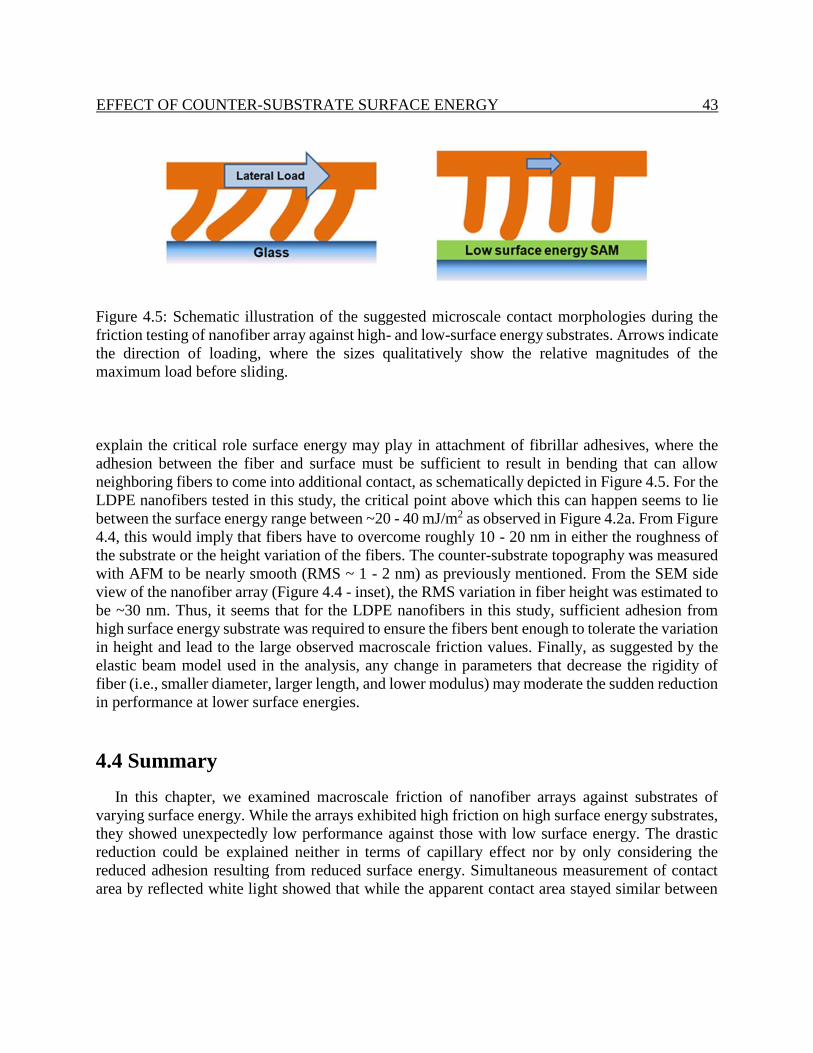
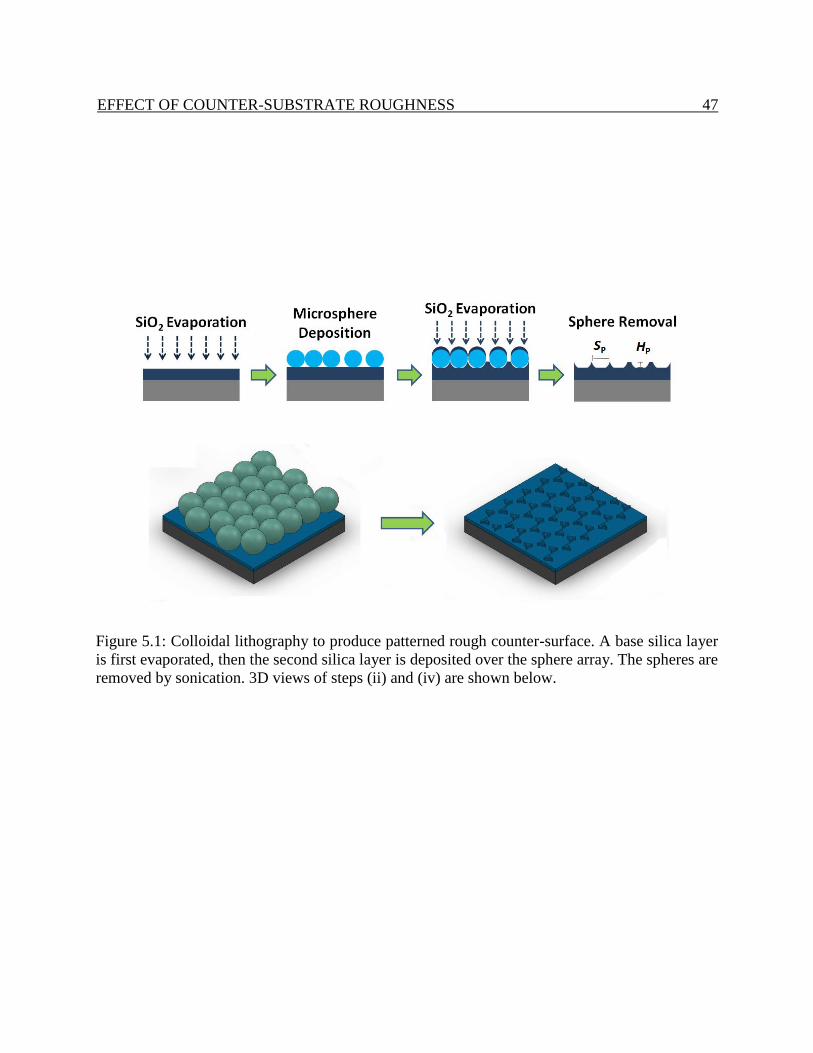
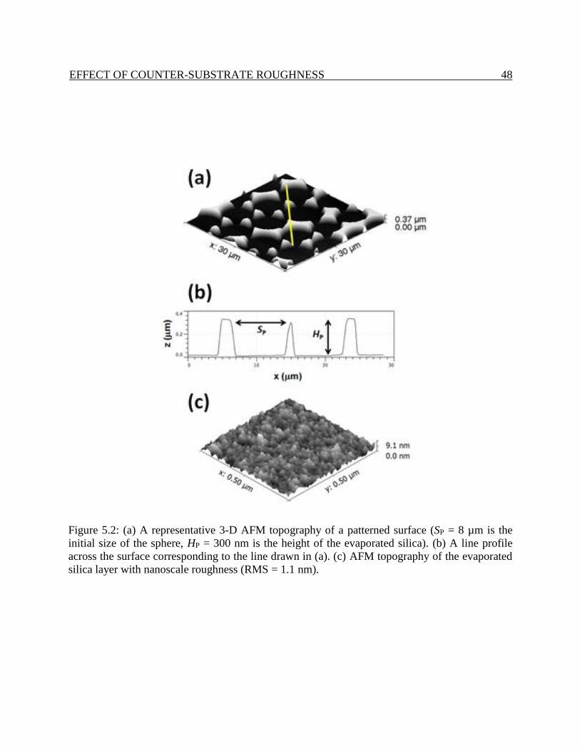
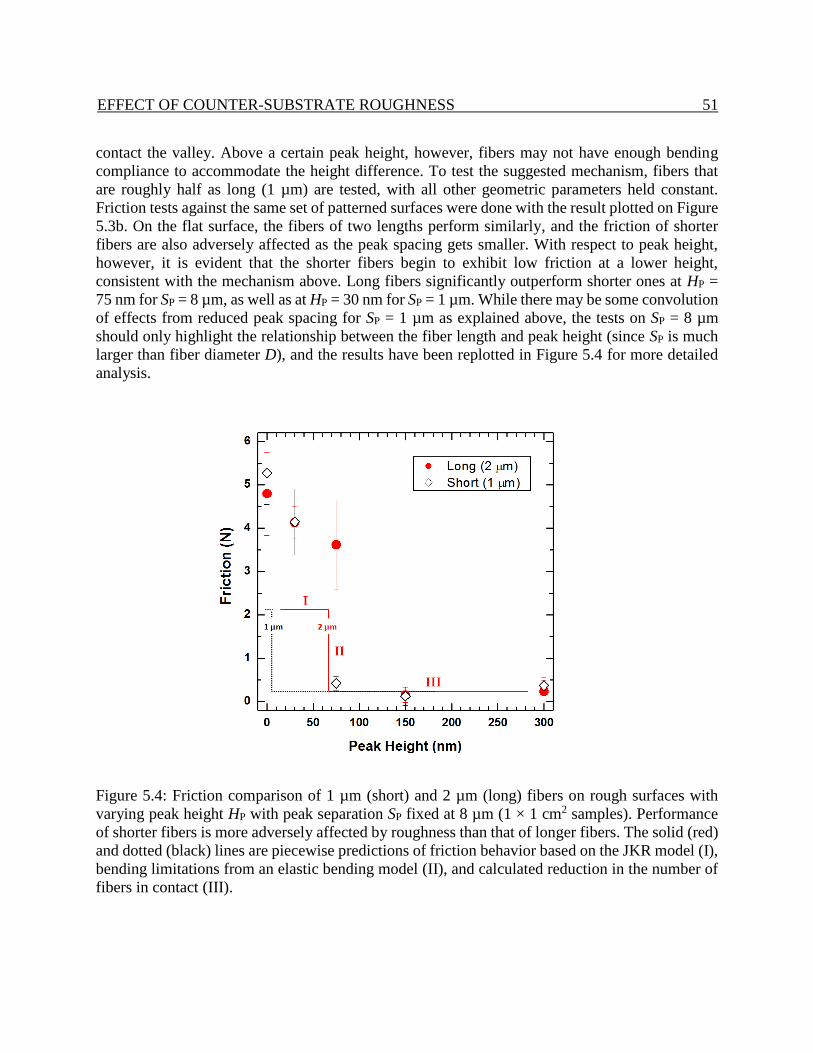
5.1 Background …...…………………………………………………………………… 44
5.2 Counter-substrate preparation …………………...………………………………… 45
5.3 Friction and roughness of counter-substrate – effect of peak spacing and height … 48
5.4 Effect of peak area fraction ..……………………………………………………… 51
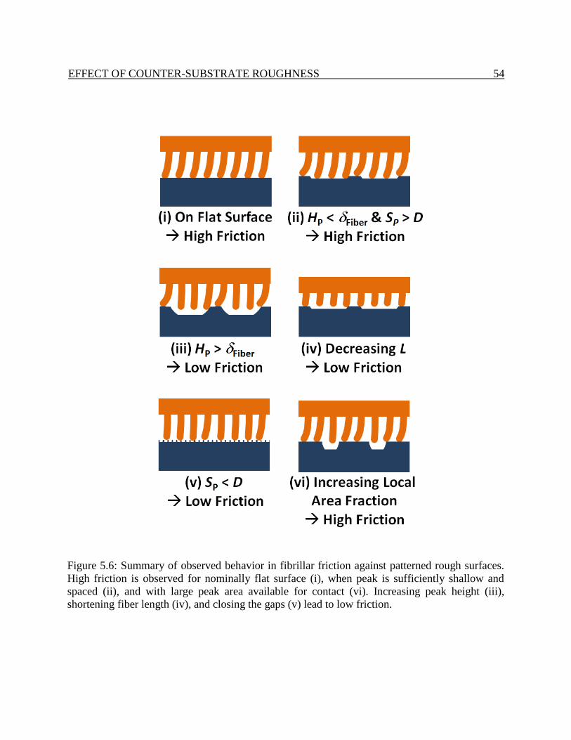
5.5 Criteria for high friction performance on rough surface ………………………….. 52
Page 6
ii
5.6 Summary ………………………………………………………………………….. 54
6 Fabrication of complex fiber designs 55
6.1 Controlling porosity, clumping, and tapering of SiNWs formed by
metal-assisted chemical etching ..…………………………………………………. 56
6.1.1 Effect of HF/H2O2 ratio ………………………………………………… 56
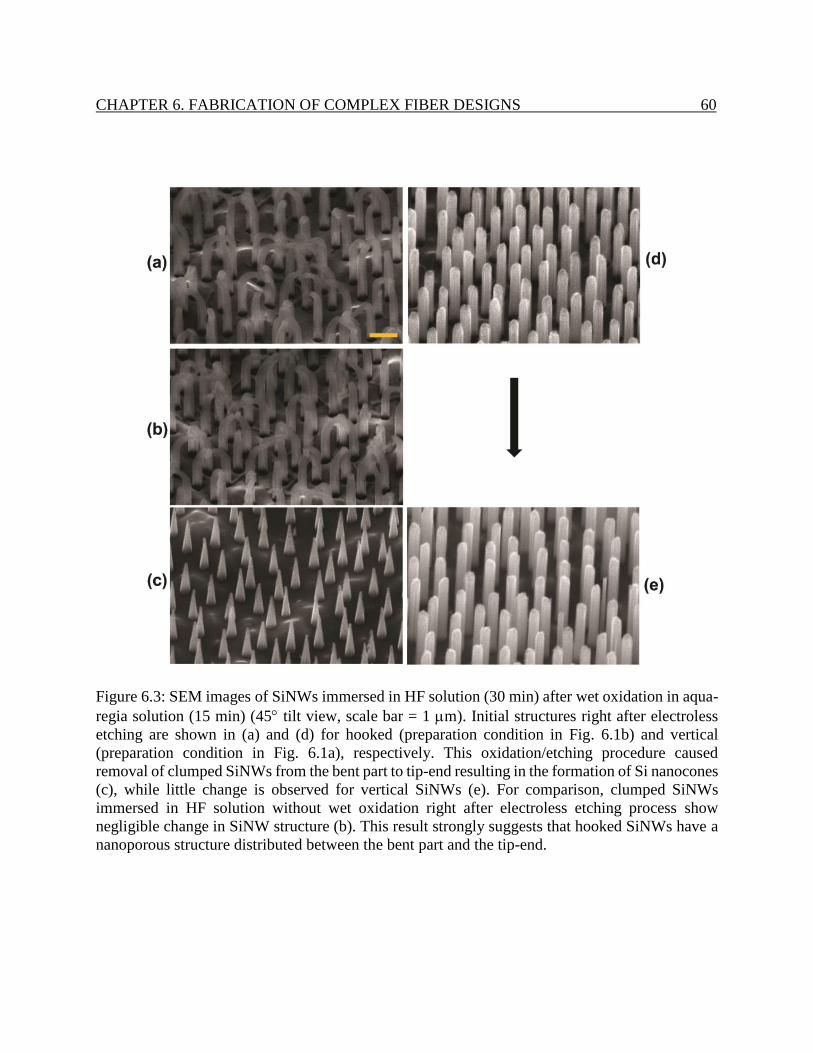
6.1.2 Nano-porosity in SiNWs ……………………………………………....… 58
6.1.3 Visualization of hole diffusion effects ………………………………….. 58
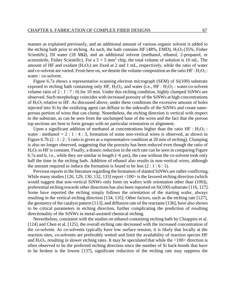
6.1.4 Regulating etching rate and clumping by electrolytes ………………….. 60
6.1.5 Summary ………………………………………………………………... 62
6.2 Controlling directionality and curvature of SiNWs by addition of co-solvent …… 65
6.2.1 Co-solvent and directionality of SiNWs ………………………………... 65
6.2.2 Etching uniformity and SiNW curvature ………………………………... 68
6.2.3 Summary ………………………………………………………………... 70
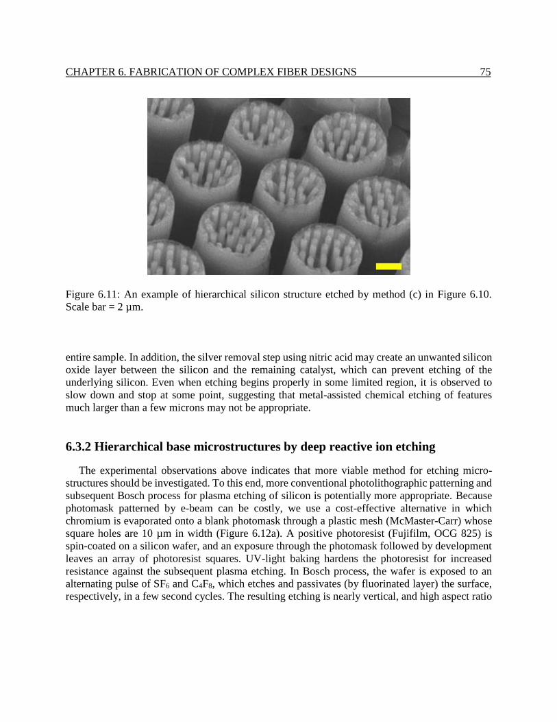
6.3 Fabrication of hierarchical structure …….………………………………………. 72
6.3.1 Hierarchical silicon micro-/nanowires by double patterning
of metal catalysts ………………………………………………….…… 72
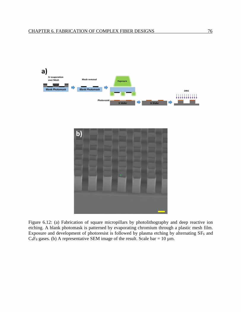
6.3.2 Hierarchical base microstructures by deep reactive ion etching ………... 74
6.4 Fabrication of composite structure ..……………………………………………… 78
6.4.1 Composite structure by utilizing polycarbonate filter ...........………….... 78
6.4.2 Composite structure with photolithography ……………………………... 78
6.5 Fabrication of tapered micropillars ……………………………………………….. 81
6.5.1 Fabrication procedure ……………………………………………………. 81
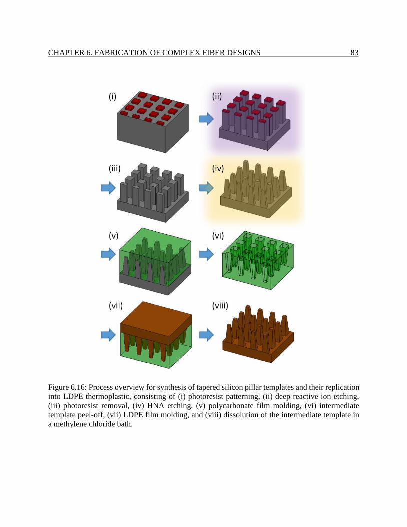
6.5.2 Fabricated silicon templates ...………………………………………….... 83
6.5.3 Friction behavior of tapered LDPE pillar array ………………………….. 86
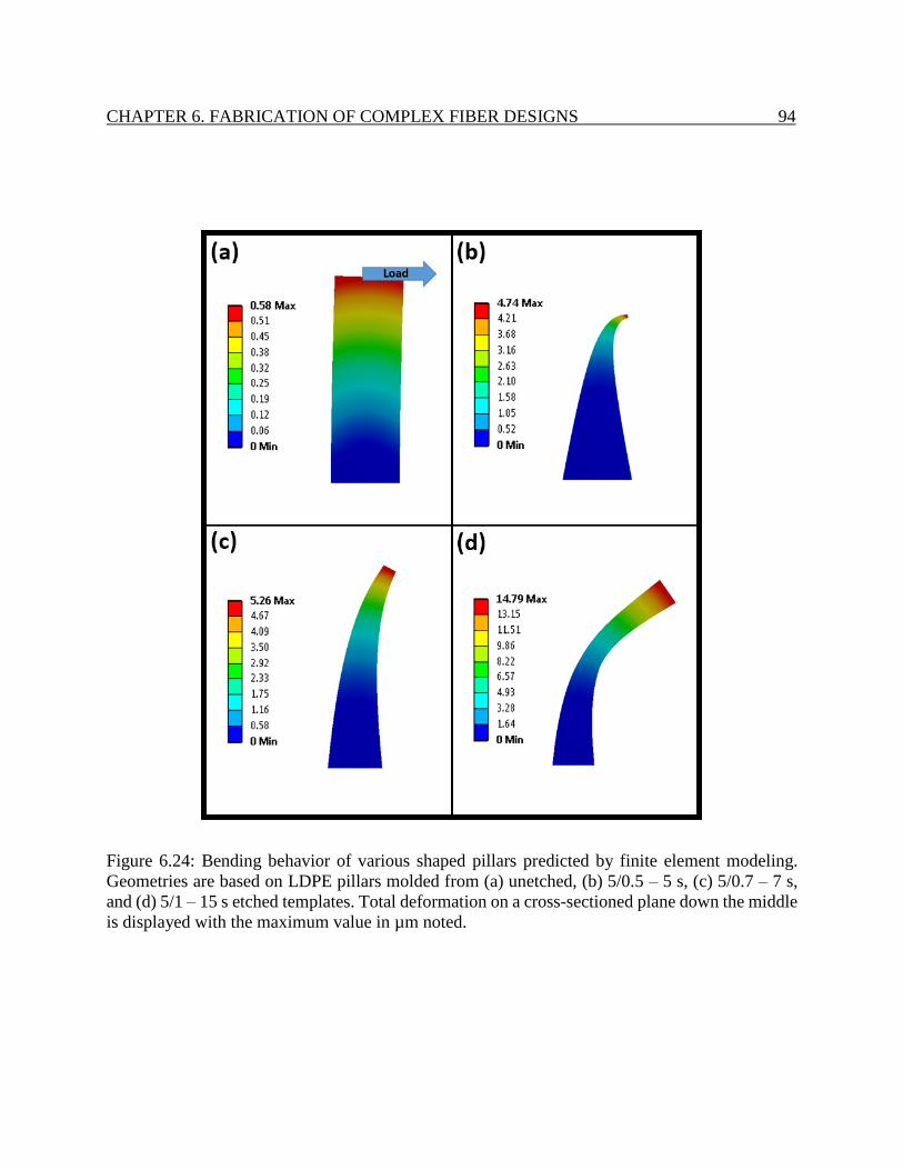
6.5.4 Comparing observed deformation behavior with finite element modelling 89
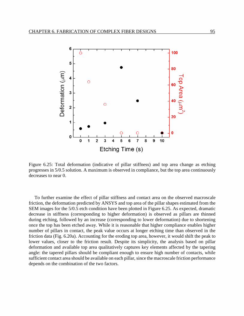
6.5.5 Summary ………………………………………………………………… 95
7 Conclusion and Future Works 96
7.1 Summary of dissertation ......…………………………………………………… 96
7.2 Future works ……………………………………………………………………… 96
Page 7
iii
Acknowledgments
I want to thank Professor Roya Maboudian for helping me have such a meaningful experience in
graduate school. I feel that I have matured so much academically and personally the last five years,
and I owe much of it to my interaction with her. Her kind and calm natured support has always
been encouraging throughout both good and challenging times. Most importantly, she always put
my interest as a student before hers, a true advisor in every sense of the word.
I am grateful to Dae Ho Lee, who has been a great mentor inside the lab and a great friend
outside, and who I respect as a hard worker and a critical thinker. I will never forget the stimulating
discussions (both scientific and completely non-scientific) and late night lab work with him.
I cannot overstate the help of the undergraduate researchers Francesca Limanto, Angela Tsao,
Mengwen Zhang, Robert Claus, Yunsie Chung, Zizhou (Joe) Zhao, Manuel Leyva, and Gina
Zaghi. Not only did I learn from and was inspired by their work ethic and intelligence, I learned a
great deal about myself through my interaction with them. I appreciate stimulating collaboration
with Kamran Shavezipur and Ye Tian on several projects. I am glad to have had a pleasant and a
lively desk neighbor, Lunet Luna. Ian Laboriante has been a great friend inside and outside the
lab. I thank Carlo Carraro for his advice and scientific insight. I am appreciative of all group
members I had the opportunity to interact with, Nicola Ferralis, Albert Gutés, Brian Bush, Greg
Doerk, Guohua Li, Fang Liu, Ben Hsia, John Alper, Maxime Vincent, Wenjuan Gou, Junqin
Zhang, Anahit Raygani, Alessandro Piotto, Nicolas Miani, Anna Harley-Trochimczyk, Peter
Lobacccaro, Shuang Wang, Shuo (Steve) Chen, Candy Chang, Marco Tocchio, Mun Sek Kim,
Nisha Mair, Ernest Chen, Brian Lee, Maxwell Fisch, Jiawen Hwang, Anton Suwandi, and Charles
Dhong.
I feel privileged to have worked with Professor Ronald Fearing, a pioneer in the topic of the
work presented here and his talented students Andrew Gillies and Paual Birkmeyer. I thank the
Center of Integrated Nanomechanical Systems, its director Willi Mickelson, and all of its
members, for broadening my perspective in the field of nanotechnology.
On a more personal note, I cherish the friendships I developed during my time in Berkeley. I
thank Eli for convincing me to finally get a smartphone in the year 2014 (and his friendship).
Kyunam, Jimmy, Chad, David, and Minsung have all enriched my life in different ways, and I am
lucky to have such great friends. I am also lucky to have been roomates with Matt Pavlovich, Zach
Baer, and Tom Dursch, who blessed me with 5 conflict-free years.
Finally, I must end the acknowledgment with the appreciation for my family. Not only have
they been motivation to finish my study, they have qualities that I admire so much that it would
not be an exaggeration to say that they have shaped me of today. My mom defines the word
resilience, and her unwavering support made possible the life I have. My brother I always consider
to be my more compassionate and optimistic half. I end this page remembering my dad, who I
know would have been very proud.
Page 8
1
Chapter 1
Introduction to gecko-inspired synthetic adhesive
1.1 Gecko adhesion
Over the last decade, geckos’ remarkable ability to stick to and climb just about any surface
found in nature has motivated a wide range of scientific interest in understanding the adhesion
mechanism of their foot-pads [1-6], as well as interest in engineering gecko-mimetic surface for
various applications [7-14]. The high adhesion and friction of its pads have been attributed to a
complex array of hairy structures, which maximize surface area for van der Waals interaction
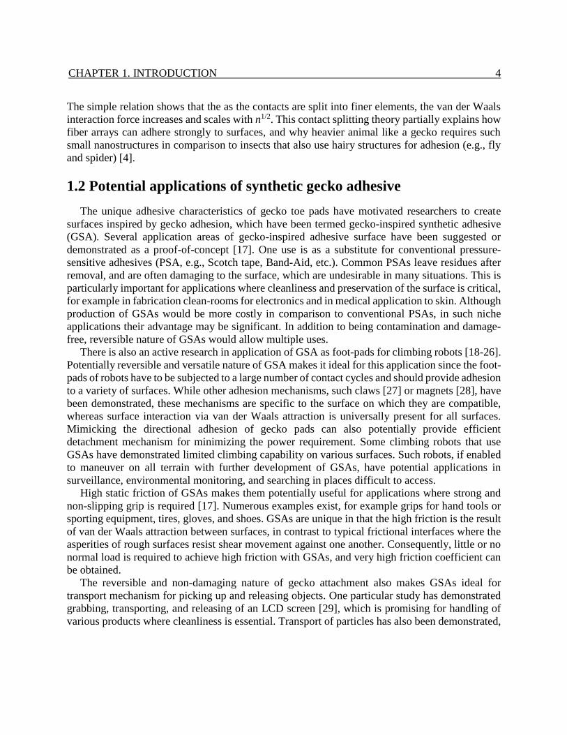
between the toes and the counter-surface [1, 2]. As shown in Figure 1.1, the pads have a hierarchy
of structures that cover various length-scales: the millimeter-sized lamellae layers, micro-sized
setae hairs, and nano-scale spatulae that terminate in thin plates that are just a few nanometers
thick.
Figure 1.1: Hierarchical structure of gecko (A) foot-hairs, ranging from the mesoscale lamellae
(B), microscale setae (C, D), and nanoscale spatulae (E). Reproduced with permission of Company
of Biologists Ltd. from [3]. Permission conveyed through Copyright Clearance Center, Inc.
Page 9
CHAPTER 1. INTRODUCTION 2
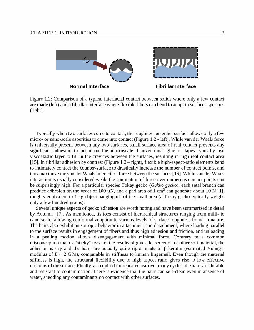
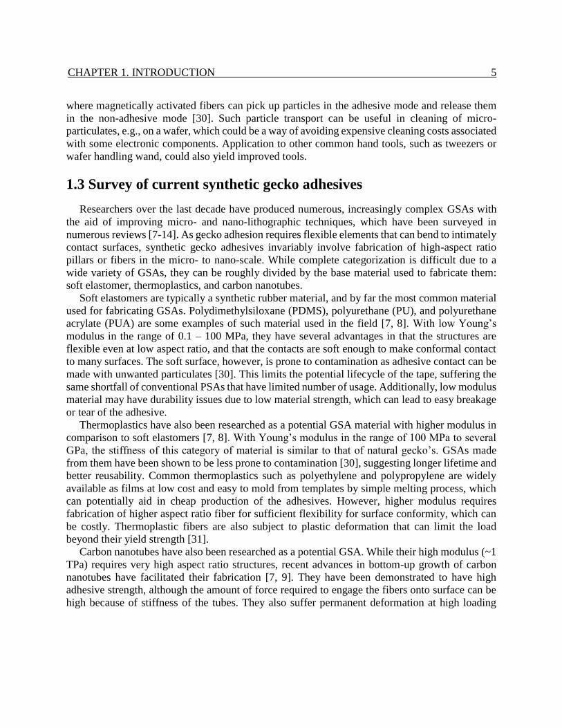
Figure 1.2: Comparison of a typical interfacial contact between solids where only a few contact
are made (left) and a fibrillar interface where flexible fibers can bend to adapt to surface asperities
(right).
Typically when two surfaces come to contact, the roughness on either surface allows only a few
micro- or nano-scale asperities to come into contact (Figure 1.2 - left). While van der Waals force
is universally present between any two surfaces, small surface area of real contact prevents any
significant adhesion to occur on the macroscale. Conventional glue or tapes typically use
viscoelastic layer to fill in the crevices between the surfaces, resulting in high real contact area
[15]. In fibrillar adhesion by contrast (Figure 1.2 – right), flexible high-aspect-ratio elements bend
to intimately contact the counter-surface to drastically increase the number of contact points, and
thus maximize the van der Waals interaction force between the surfaces [16]. While van der Waals
interaction is usually considered weak, the summation of force over numerous contact points can
be surprisingly high. For a particular species Tokay gecko (Gekko gecko), each setal branch can
produce adhesion on the order of 100 µN, and a pad area of 1 cm2 can generate about 10 N [1],
roughly equivalent to 1 kg object hanging off of the small area (a Tokay gecko typically weighs
only a few hundred grams).
Several unique aspects of gecko adhesion are worth noting and have been summarized in detail
by Autumn [17]. As mentioned, its toes consist of hierarchical structures ranging from milli- to
nano-scale, allowing conformal adaption to various levels of surface roughness found in nature.
The hairs also exhibit anisotropic behavior in attachment and detachment, where loading parallel
to the surface results in engagement of fibers and thus high adhesion and friction, and unloading
in a peeling motion allows disengagement with minimal force. Contrary to a common
misconception that its “sticky” toes are the results of glue-like secretion or other soft material, the
adhesion is dry and the hairs are actually quite rigid, made of β-keratin (estimated Young’s
modulus of E ~ 2 GPa), comparable in stiffness to human fingernail. Even though the material
stiffness is high, the structural flexibility due to high aspect ratio gives rise to low effective
modulus of the surface. Finally, as required for repeated use over many cycles, the hairs are durable
and resistant to contamination. There is evidence that the hairs can self-clean even in absence of
water, shedding any contaminants on contact with other surfaces.
Page 10
CHAPTER 1. INTRODUCTION 3
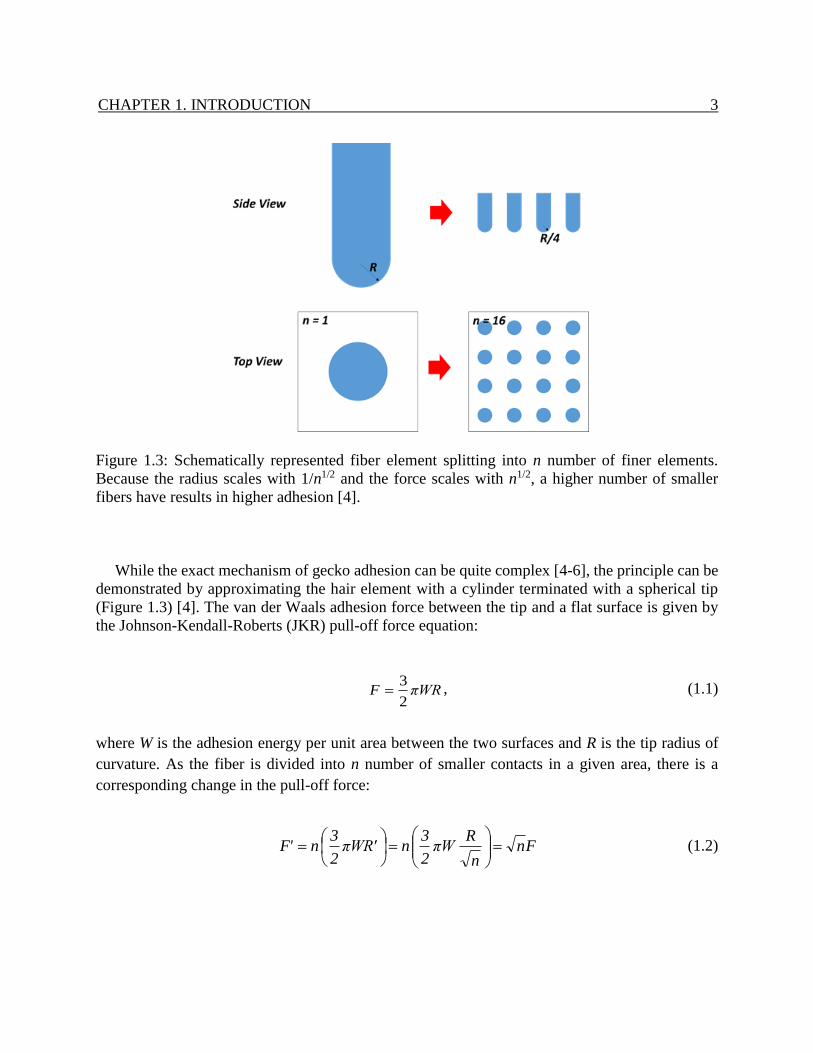
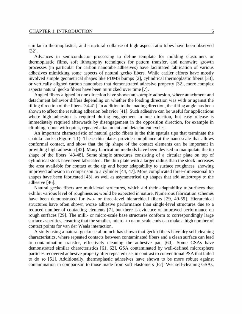
Figure 1.3: Schematically represented fiber element splitting into n number of finer elements.
Because the radius scales with 1/n1/2 and the force scales with n1/2, a higher number of smaller
fibers have results in higher adhesion [4].
While the exact mechanism of gecko adhesion can be quite complex [4-6], the principle can be
demonstrated by approximating the hair element with a cylinder terminated with a spherical tip
(Figure 1.3) [4]. The van der Waals adhesion force between the tip and a flat surface is given by
the Johnson-Kendall-Roberts (JKR) pull-off force equation:
πWRF2
3 , (1.1)
where W is the adhesion energy per unit area between the two surfaces and R is the tip radius of
curvature. As the fiber is divided into n number of smaller contacts in a given area, there is a
corresponding change in the pull-off force:
(1.2)
Fnn
RπW
2
3nπWR'
2
3nF'
Page 11
CHAPTER 1. INTRODUCTION 4
The simple relation shows that the as the contacts are split into finer elements, the van der Waals
interaction force increases and scales with n1/2. This contact splitting theory partially explains how
fiber arrays can adhere strongly to surfaces, and why heavier animal like a gecko requires such
small nanostructures in comparison to insects that also use hairy structures for adhesion (e.g., fly
and spider) [4].
1.2 Potential applications of synthetic gecko adhesive
The unique adhesive characteristics of gecko toe pads have motivated researchers to create
surfaces inspired by gecko adhesion, which have been termed gecko-inspired synthetic adhesive
(GSA). Several application areas of gecko-inspired adhesive surface have been suggested or
demonstrated as a proof-of-concept [17]. One use is as a substitute for conventional pressure-
sensitive adhesives (PSA, e.g., Scotch tape, Band-Aid, etc.). Common PSAs leave residues after
removal, and are often damaging to the surface, which are undesirable in many situations. This is
particularly important for applications where cleanliness and preservation of the surface is critical,
for example in fabrication clean-rooms for electronics and in medical application to skin. Although
production of GSAs would be more costly in comparison to conventional PSAs, in such niche
applications their advantage may be significant. In addition to being contamination and damage-
free, reversible nature of GSAs would allow multiple uses.
There is also an active research in application of GSA as foot-pads for climbing robots [18-26].
Potentially reversible and versatile nature of GSA makes it ideal for this application since the foot-
pads of robots have to be subjected to a large number of contact cycles and should provide adhesion
to a variety of surfaces. While other adhesion mechanisms, such claws [27] or magnets [28], have
been demonstrated, these mechanisms are specific to the surface on which they are compatible,
whereas surface interaction via van der Waals attraction is universally present for all surfaces.
Mimicking the directional adhesion of gecko pads can also potentially provide efficient
detachment mechanism for minimizing the power requirement. Some climbing robots that use
GSAs have demonstrated limited climbing capability on various surfaces. Such robots, if enabled
to maneuver on all terrain with further development of GSAs, have potential applications in
surveillance, environmental monitoring, and searching in places difficult to access.
High static friction of GSAs makes them potentially useful for applications where strong and
non-slipping grip is required [17]. Numerous examples exist, for example grips for hand tools or
sporting equipment, tires, gloves, and shoes. GSAs are unique in that the high friction is the result
of van der Waals attraction between surfaces, in contrast to typical frictional interfaces where the
asperities of rough surfaces resist shear movement against one another. Consequently, little or no
normal load is required to achieve high friction with GSAs, and very high friction coefficient can
be obtained.
The reversible and non-damaging nature of gecko attachment also makes GSAs ideal for
transport mechanism for picking up and releasing objects. One particular study has demonstrated
grabbing, transporting, and releasing of an LCD screen [29], which is promising for handling of
various products where cleanliness is essential. Transport of particles has also been demonstrated,
Page 12
CHAPTER 1. INTRODUCTION 5
where magnetically activated fibers can pick up particles in the adhesive mode and release them
in the non-adhesive mode [30]. Such particle transport can be useful in cleaning of micro-
particulates, e.g., on a wafer, which could be a way of avoiding expensive cleaning costs associated
with some electronic components. Application to other common hand tools, such as tweezers or
wafer handling wand, could also yield improved tools.
1.3 Survey of current synthetic gecko adhesives
Researchers over the last decade have produced numerous, increasingly complex GSAs with
the aid of improving micro- and nano-lithographic techniques, which have been surveyed in
numerous reviews [7-14]. As gecko adhesion requires flexible elements that can bend to intimately
contact surfaces, synthetic gecko adhesives invariably involve fabrication of high-aspect ratio
pillars or fibers in the micro- to nano-scale. While complete categorization is difficult due to a
wide variety of GSAs, they can be roughly divided by the base material used to fabricate them:
soft elastomer, thermoplastics, and carbon nanotubes.
Soft elastomers are typically a synthetic rubber material, and by far the most common material
used for fabricating GSAs. Polydimethylsiloxane (PDMS), polyurethane (PU), and polyurethane
acrylate (PUA) are some examples of such material used in the field [7, 8]. With low Young’s
modulus in the range of 0.1 – 100 MPa, they have several advantages in that the structures are
flexible even at low aspect ratio, and that the contacts are soft enough to make conformal contact
to many surfaces. The soft surface, however, is prone to contamination as adhesive contact can be
made with unwanted particulates [30]. This limits the potential lifecycle of the tape, suffering the
same shortfall of conventional PSAs that have limited number of usage. Additionally, low modulus
material may have durability issues due to low material strength, which can lead to easy breakage
or tear of the adhesive.
Thermoplastics have also been researched as a potential GSA material with higher modulus in
comparison to soft elastomers [7, 8]. With Young’s modulus in the range of 100 MPa to several
GPa, the stiffness of this category of material is similar to that of natural gecko’s. GSAs made
from them have been shown to be less prone to contamination [30], suggesting longer lifetime and
better reusability. Common thermoplastics such as polyethylene and polypropylene are widely
available as films at low cost and easy to mold from templates by simple melting process, which
can potentially aid in cheap production of the adhesives. However, higher modulus requires
fabrication of higher aspect ratio fiber for sufficient flexibility for surface conformity, which can
be costly. Thermoplastic fibers are also subject to plastic deformation that can limit the load
beyond their yield strength [31].
Carbon nanotubes have also been researched as a potential GSA. While their high modulus (~1
TPa) requires very high aspect ratio structures, recent advances in bottom-up growth of carbon
nanotubes have facilitated their fabrication [7, 9]. They have been demonstrated to have high
adhesive strength, although the amount of force required to engage the fibers onto surface can be
high because of stiffness of the tubes. They also suffer permanent deformation at high loading
Page 13
CHAPTER 1. INTRODUCTION 6
similar to thermoplastics, and structural collapse of high aspect ratio tubes have been observed
[32].
Advances in semiconductor processing to define template for molding elastomers or
thermoplastic films, soft lithography techniques for pattern transfer, and nanowire growth
processes (in particular for carbon nanotube adhesives) have facilitated fabrication of various
adhesives mimicking some aspects of natural gecko fibers. While earlier efforts have mostly
involved simple geometrical shapes like PDMS bumps [2], cylindrical thermoplastic fibers [33],
or vertically aligned carbon nanotubes that demonstrated adhesive property [32], more complex
aspects natural gecko fibers have been mimicked over time [7].
Angled fibers aligned in one direction have shown anisotropic adhesion, where attachment and
detachment behavior differs depending on whether the loading direction was with or against the
tilting direction of the fibers [34-41]. In addition to the loading direction, the tilting angle has been
shown to affect the resulting adhesion behavior [41]. Such adhesive can be useful for applications
where high adhesion is required during engagement in one direction, but easy release is
immediately required afterwards by disengagement in the opposition direction, for example in
climbing robots with quick, repeated attachment and detachment cycles.
An important characteristic of natural gecko fibers is the thin spatula tips that terminate the
spatula stocks (Figure 1.1). These thin plates provide compliance at the nano-scale that allows
conformal contact, and show that the tip shape of the contact elements can be important in
providing high adhesion [42]. Many fabrication methods have been devised to manipulate the tip
shape of the fibers [43-48]. Some simple structures consisting of a circular plate on top of
cylindrical stock have been fabricated. The thin plate with a larger radius than the stock increases
the area available for contact at the tip and better adaptability to surface roughness, showing
improved adhesion in comparison to a cylinder [44, 47]. More complicated three-dimensional tip
shapes have been fabricated [43], as well as asymmetrical tip shapes that add anisotropy to the
adhesive [46].
Natural gecko fibers are multi-level structures, which aid their adaptability to surfaces that
exhibit various level of roughness as would be expected in nature. Numerous fabrication schemes
have been demonstrated for two- or three-level hierarchical fibers [29, 49-59]. Hierarchical
structures have often shown worse adhesive performance than single-level structures due to a
reduced number of contacting elements [7], but there is evidence of improved performance on
rough surfaces [29]. The milli- or micro-scale base structures conform to correspondingly large
surface asperities, ensuring that the smaller, micro- to nano-scale ends can make a high number of
contact points for van der Waals interaction.
A study using a natural gecko setal branch has shown that gecko fibers have dry self-cleaning
characteristics, where repeated contacts between contaminated fibers and a clean surface can lead
to contamination transfer, effectively cleaning the adhesive pad [60]. Some GSAs have
demonstrated similar characteristics [61, 62]. GSA contaminated by well-defined microsphere
particles recovered adhesive property after repeated use, in contrast to conventional PSA that failed
to do so [61]. Additionally, thermoplastic adhesives have shown to be more robust against
contamination in comparison to those made from soft elastomers [62]. Wet self-cleaning GSAs,
Page 14
CHAPTER 1. INTRODUCTION 7
where water can absorb surface contaminants and roll off, has also been shown to be an effective
mode of self-cleaning [47, 63].
As briefly overviewed, there has been an impressive progress in regard to fabrication of new
structures that mimic one or more aspects of natural gecko adhesion. However, limitation in
lithography technology have prevented producing synthetic gecko adhesive that closely imitates
the versatile and durable performance of natural gecko pads. Furthermore, adhesion and friction
behavior of fibrillar surface is still poorly understood. Rather than focusing the entire effort on
fabrication of structure that matches that of natural gecko, which would be costly in both research
and in production, a more reasonable approach would be to study parameters that affect the
interfacial behavior in order to aid in rational design. The next section will describe some of the
challenges that need to be met in order to successfully replicate the versatile performance of natural
gecko pads.
1.4 Current challenges of GSAs
Although many GSAs have shown adhesion and friction performance comparable to that of a
natural gecko, almost all testing of GSAs has been done in ideal laboratory settings, in particular
on smooth glass free of contamination [7-10]. Surfaces encountered in application present
additional complications due to roughness, variation in surface energy, and contamination. On a
smooth surface, all fibers on typical GSAs can easily contact the surface, but introduction of
various levels of roughness have shown to dramatically reduce the adhesion or friction of GSAs
[18, 29, 47, 50, 64]. Because most of surfaces encountered in applications have some level of
roughness, GSAs must be improved to adapt to asperities on surfaces.
Glass is ideal for high adhesion because of its high surface energy. The higher the surface
energy, the more thermodynamically unstable the surface, which results in stronger adhesion to
another surface (in this case the contacting tips of the fiber structures) [65]. While metal and
ceramics typically have high surface energy (several J/m2 for a fresh cleaved surface, but closer to
the order of 100 mJ/m2 in a laboratory setting), many common surfaces (e.g., wood, painted wall,
contaminated surface) have lower surface energy falling in the range of 30 – 60 mJ/m2 [65-68].
Some hydrophobic surfaces, for example Teflon coating, can have surface energy below 20 mJ/m2
[65]. To have a truly gecko-like adhesive, the GSA should be able to adhere to surfaces with a
wide range of surface energy.
Other practical considerations include durability and contaminations during multiple use. While
natural gecko foot-hairs can withstand thousands of step cycles without significant wear, limited
testing has been performed on GSAs durability over repeated usage. Because reversible attachment
is a key advantage of GSAs, durability remains an important issue. Surfaces in real application
could also present various sources of contamination (dust particles, oily residues, etc.) that can
degrade the performance of the adhesive over multiple cycles. While natural geckos have robust
design against such contamination [60], limited studies have been done on GSA contamination
and how to mitigate the issue.
Page 15
CHAPTER 1. INTRODUCTION 8
It is worth noting that adhesive and frictional behavior of fibrillar surface is poorly understood.
Effects of even the most fundamental parameters like the length and diameter of the fibers on
fibillar adhesive have been a subject of debate, and limited experimental data exist [7]. Still less
study has been done on rough and low-energy surfaces, even though they present critical
challenges in application as mentioned. Finally, most experimental studies of GSAs have been
performed with soft elastomers, which are adhesive without any high aspect ratio structuring due
to the low Young’s modulus. Thermoplastic materials that are closer to the stiffness of natural
gecko hairs have not received as much focus, and they have potential to be true to the principle of
gecko-like adhesive, where strong attachment is enabled by structuring the surface with compliant
elements.
1.5 Outline of work presented
This dissertation presents fabrication and experimental study of the interfacial behavior of
gecko-inspired thermoplastic fibrillar adhesives. Chapter 2 begins by describing the overall
fabrication process, including the method to chemically etch silicon nanowire (SiNW) array, which
serves as the molding template for creating thermoplastic replica that exhibit adhesive
characteristics. The testing method to characterize the adhesive strength of the nanofibrillar surface
will be explained, focusing on the friction force of macro-sized samples.
The next three chapters focus on better understanding a fibrillar interface by examining factors
that critically affect the friction performance of the fabricated GSA. In Chapter 2, two basic fiber
geometric parameters, length and diameter, are varied to study their effect on the macroscale
friction of the fibrillar array and optimized for high friction on smooth glass. Chapters 3 and 4
investigate fibrillar friction on non-ideal surfaces, where lower surface energy and roughness will
each be introduced in a controlled manner to provide insights on why GSAs often fail under these
conditions.
The last chapter presents fabrication schemes for more complex fiber designs. For the chemical
etching of SiNW template, various aspects of etching chemistry are explored to control the
resulting SiNW morphology. Control over geometrical factors like aspect ratio, clumping, tapering,
and directionality of the SiNW is presented. Fabrication of single-level fiber will be extended to
produce hierarchical fiber designs, and composite fibrillar adhesive material composed of
thermoplastic and soft elastomer is presented. A method to control the tapering of high aspect ratio
structure is demonstrated, which allows fabrication of more complex shaped fibers. The
dissertation concludes with future work to be done in relation to the presented work.
Page 16
9
Chapter 2
Template fabrication and friction test setup
This chapter is reproduced in part with permission from: Y. Kim, R. K. Claus, F. Limanto, R.
S. Fearing, R. Maboudian. Friction characteristics of polymeric nanofiber arrays against substrates
with tailored geometry. Langmuir 2013, 29, 8395-8401 <http://pubs.acs.org/articlesonrequest
/AOR-zasD6r7JwTvaZcEnujbF>; Y. Kim, F. Limanto, D. H. Lee, R. S. Fearing, R. Maboudian.
Role of counter-substrate surface energy in macroscale friction of nanofiber arrays. Langmuir 2012,
28, 2922-2927 < http://pubs.acs.org/articlesonrequest/AOR-8mRysJmZEiGJ5335qbxK>; D. H.
Lee, Y. Kim, R. S. Fearing, R. Maboudian. Effect of fiber geometry on macroscale friction of
ordered low-density polyethylene nanofiber arrays. Langmuir 2011, 27, 11008-11016 < http://pubs.acs.org/articlesonrequest/AOR-JyXIubdUfFwS7RPMqJG8>. Copyright 2011, 2012,
2013 American Chemical Society.
A systematic study of fibrillar interface first requires a consistent micro/nano-fabrication
method for defining a regular array of polymer fibers with control over important geometrical
factors like fiber number density and aspect ratio. In comparison to direct patterning of polymer
micro/nano-fabrication techniques of silicon are much more researched owing to its applications
in areas such as integrated circuits, micro-electro-mechanical systems, and renewable energy
devices. Therefore, it is a sensible approach to first define an array of high aspect ratio silicon
structures, for example SiNWs, and transfer the pattern to a polymer by various molding processes.
This is particularly useful for thermoplastics, since they can be easily molded from a template by
a simple melting process. The following sections describe the process for fabrication low-density
polyethylene nanofibers by molding from SiNW templates. A description of method for friction
testing of the fabricated GSA is then presented.
2.1 Fabrication process overview
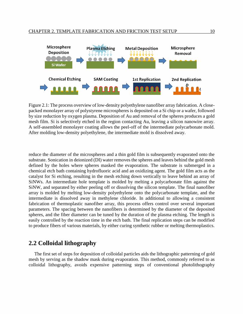
The fabrication process is shown in Figure 2.1 [69-71]. The procedure is first briefly described
in this section, and the detailed explanation of significant parts of the process follows. The process
begins by floating a monolayer of packed polystyrene (PS) microspheres on water and transferring
it onto a silicon chip (typically 1 × 1 cm2) or a wafer. Oxygen plasma is used to etch and
Page 17
CHAPTER 2. TEMPLATE FABRICATION AND FRICTION TEST SETUP 10
Figure 2.1: The process overview of low-density polyethylene nanofiber array fabrication. A close-
packed monolayer array of polystyrene microspheres is deposited on a Si chip or a wafer, followed
by size reduction by oxygen plasma. Deposition of Au and removal of the spheres produces a gold
mesh film. Si is selectively etched in the region contacting Au, leaving a silicon nanowire array.
A self-assembled monolayer coating allows the peel-off of the intermediate polycarbonate mold.
After molding low-density polyethylene, the intermediate mold is dissolved away.
reduce the diameter of the microspheres and a thin gold film is subsequently evaporated onto the
substrate. Sonication in deionized (DI) water removes the spheres and leaves behind the gold mesh
defined by the holes where spheres masked the evaporation. The substrate is submerged in a
chemical etch bath containing hydrofluoric acid and an oxidizing agent. The gold film acts as the
catalyst for Si etching, resulting in the mesh etching down vertically to leave behind an array of
SiNWs. An intermediate hole template is molded by melting a polycarbonate film against the
SiNW, and separated by either peeling off or dissolving the silicon template. The final nanofiber
array is molded by melting low-density polyethylene onto the polycarbonate template, and the
intermediate is dissolved away in methylene chloride. In additional to allowing a consistent
fabrication of thermoplastic nanofiber array, this process offers control over several important
parameters. The spacing between the nanofibers is determined by the diameter of the deposited
spheres, and the fiber diameter can be tuned by the duration of the plasma etching. The length is
easily controlled by the reaction time in the etch bath. The final replication steps can be modified
to produce fibers of various materials, by either curing synthetic rubber or melting thermoplastics.
2.2 Colloidal lithography
The first set of steps for deposition of colloidal particles aids the lithographic patterning of gold
mesh by serving as the shadow mask during evaporation. This method, commonly referred to as
colloidal lithography, avoids expensive patterning steps of conventional photolithography
Page 18
CHAPTER 2. TEMPLATE FABRICATION AND FRICTION TEST SETUP 11
Figure 2.2: The procedure for depositing a monolayer of hexagonally-packed polystyrene
microspheres. A water solution containing polystyrene is carefully introduced to water/air
interface, where the spheres float. The spheres are packed by a small amount of surfactant, and
subsequently transferred to a silicon chip/wafer.
and is especially useful for producing repeating patterns of small size [72]. To begin the procedure,
a Si(100) wafer chip of ~1×1 cm2 size or a wafer are cleaned by successive sonication in acetone
and isopropanol for 10 min. each, followed by UV ozone cleaning for another 10 min. All Si
substrate used are purchased from either Universitywafer (p-type, 1 - 30 Ω-cm) or Silicon Quest
International (p-type, 10 - 30 Ω-cm). Cleaned Si substrate is thoroughly washed with deionized
(DI) water (18 MΩ), then blow dried by N2 gas. PS microsphere array is deposited on the Si
substrate by a simple float and transfer technique, as shown in Figure 2.2.
Commercially purchased monodispersed microsphere solution (Duke Scientific, 10 wt% in
water) is first diluted by DI water (to 2 wt%) and mixed with ethanol (1 : 1 volume ratio). The
solution is carefully introduced with a pipet to a NaCl solution (~0.5 wt% in distilled water), which
produces a disordered film of floating PS microspheres. PS pheres of a wide range of diameter can
be floated (500 nm – 10 µm), but larger sized spheres require additional hexane layer on water
bath to prevent a significant number of spheres from sinking into the bulk water. The floated
spheres can be pushed into a close-packed monolayer film with the addition of a small droplet (a
few µL) of a surfactant solution (sodium dodecylsulfate, 3 wt% in distilled water). The array is
then transferred to the Si substrate by a micro-manipulating setup based on a stepping motor used
for controlled motion of the substrate during immersion and withdrawals (~2 mm/sec). Close-
packed PS microsphere arrays on Si surface could be obtained over a large area (up to 4” wafer-
scale) as seen from the scanning electron microscope (SEM) image (JEOL JSM 6490LV, Agilent
NovelX-MySEM, or LEO 1550 is used to take the SEM images presented throughout this
dissertation) and a picture of the wafer covered by the monolayer (Figure 2.3 - left). While similar
to the Langmuir-Blodgett trough method for depositing monolayers, this method uses a small
amount of surfactant, rather than a mechanical trough, for packing the monolayer. After the
Page 19
CHAPTER 2. TEMPLATE FABRICATION AND FRICTION TEST SETUP 12
Figure 2.3: SEM images of microspheres in a hexagonal arrangement before oxygen plasma
etching (left) and after oxygen plasma etching (right). Inset shows the spheres can be deposited on
a 4” wafer scale.
deposition, the microspheres are reduced in size (Figure 2.3 - right) by oxygen plasma treatment,
which produces a non-close packed array. For most of this work, the diameter of the deposited
microsphere is 1 µm, also resulting in center-to-center spacing of 1 µm in a hexagonal arrangement.
2.3 Metal-catalyzed electroless etching of silicon template
This section contains material from the following publication with permission from the
contributing authors: D. H. Lee, Y. Kim, G. S. Doerk, I. Laboriante, R. Maboudian. Strategies for
controlling Si nanowire formation during Au-assisted electroless etching. J. Mater. Chem. 2011,
21, 10359-10363. <http:/dx.doi.org/10.1039/C1JM11164G>. Reproduced by permission of The
Royal Society of Chemistry (RSC).
Once the spheres are reduced in size by plasma treatment (Plasma-Therm PK-12 RIE, 30 W,
100 SCCM), a thin layer of gold (20 nm) is evaporated (Thermionics VE-100) and the spheres are
removed by sonication in DI water (any oxide layer formed during the processing is removed by
10 min of vapor HF exposure prior to evaporation and 5 to 10 min of liquid HF treatment after the
sphere removal). This produces a gold mesh defined by the holes where spheres have initially been
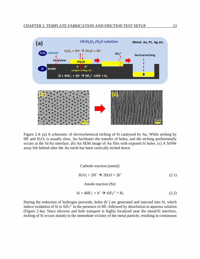
placed (Figure 2.4b). Gold is a catalyst in chemical etching of silicon by HF and an oxidizing agent,
in this case hydrogen peroxide. While uncatalyzed Si etching in HF/H2O2 solution is rather slow,
the electrochemical reaction is greatly accelerated in the presence of metal catalysts such as Au,
Ag, and Pt, which are more electronegative than Si, where the metals can accept electrons from Si
and donate electrons to H2O2. This etching is generally understood to be a localized
electrochemical process, with the metal acting as a local cathodic site and the underlying Si as a
local anodic site as follows [73]:
Page 20
CHAPTER 2. TEMPLATE FABRICATION AND FRICTION TEST SETUP 13
Figure 2.4: (a) A schematic of electrochemical etching of Si catalyzed by Au. While etching by
HF and H2O2 is usually slow, Au facilitates the transfer of holes, and the etching preferentially
occurs at the Si/Au interface. (b) An SEM image of Au film with exposed Si holes. (c) A SiNW
array left behind after the Au mesh has been vertically etched down.
Cathode reaction (metal):
H2O2 + 2H+ 2H2O + 2h+ (2.1)
Anode reaction (Si):
Si + 4HF2- + h+ SiF6
2- + H2 (2.2)
During the reduction of hydrogen peroxide, holes (h+) are generated and injected into Si, which
induce oxidation of Si to SiF62- in the presence of HF, followed by dissolution in aqueous solution
(Figure 2.4a). Since electron and hole transport is highly localized near the metal/Si interface,
etching of Si occurs mainly in the immediate vicinity of the metal particle, resulting in continuous
Page 21
CHAPTER 2. TEMPLATE FABRICATION AND FRICTION TEST SETUP 14
sinking of the metal and the formation of high-aspect ratio nanostructures [73]. In our case, the
patterned gold mesh sinks down, leaving behind an array of silicon nanowires (Figure 2.4c).
Many factors affecting the final Si nanostructures have been studied such as the type of metal
(e.g., Ag, Au, Pt), the HF and H2O2 concentrations, the substrate doping level, crystal orientation
of the substrate, and etching temperature [73]. Later sections (6.1 and 6.2) will present variations
in the etching conditions that critically affect SiNW morphology. For now, the etching bath
consists of a fixed amount of HF (48 wt%, EMD), H2O2 (35 %, Fisher Scientific), DI water, and
acetonitrile (Fisher Scientific) in the volume ratio 2:1:5:2, respectively, where acetonitrile is added
as a wetting agent that improves the etching uniformity across the substrate. The total volume of
solution is typically 10 mL for each 1 × 1 cm2 chip, although the volume of solution has little effect
on the etching behavior as long as enough reactants are present for the etching duration. This
composition produces an array of vertical, untapered SiNWs, suitable as a template for molding a
well-defined thermoplastic fiber array.
2.4 Nanostructure molding
The SiNW pattern is transferred to thermoplastic by simple vacuum molding steps. The gold
catalyst layer is first removed by soaking in an aqua regia bath (a mix of 38% hydrochloric and
70% nitric acid in 3:1 volume ratio) for a few minutes. To aid the separation from the template,
SiNWs are first treated by octadecyltrichlorosilane, a self-assembled monolayer easily prepared
by reaction in the liquid phase. The substrate is submerged in a bath containing 1:1000 volume
ratio of octadecyltrichlorosilane (Sigma-Aldrich) to toluene (Fisher Scientific) for 15 hr, which
covers the surface of the SiNWs with a hydrocarbon layer. Typical solution volume is about 5 mL
of toluene for each 1 × 1 cm2. An intermediate hole template is molded by melting a polycarbonate
film (McMaster-Carr, 100 µm thick) against the SiNW template in vacuum at 300 °C for 1.5 hr.
Once cooled to room temperature, the film is mechanically peeled-off from the template.
Alternatively in cases where peel-off is difficult due to high aspect ratio, Si template can be
dissolved away with a silicon etchant (typically acidic solution containing HF and nitric acid). The
nanofiber array replica is molded by melting low-density polyethylene (LDPE, McMaster-Carr,
100 µm thick film) into the polycarbonate template at 160 °C for 1 hr. Physical separation of the
films at this point is undesirable due to plastic yielding of LDPE fibers. Instead, the polycarbonate
intermediate is dissolved away in a methylene chloride (Fisher Scientific) bath for 1 hr, followed
by additional soaking in methylene chloride for 10 min. An isopropanol rinse and N2 blow drying
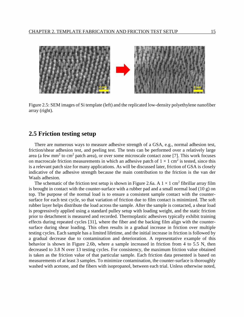
complete the fabrication process. Representative SEM images of a template and the replicated
LDPE fibers are shown in Figure 2.5.
Page 22
CHAPTER 2. TEMPLATE FABRICATION AND FRICTION TEST SETUP 15
Figure 2.5: SEM images of Si template (left) and the replicated low-density polyethylene nanofiber
array (right).
2.5 Friction testing setup
There are numerous ways to measure adhesive strength of a GSA, e.g., normal adhesion test,
friction/shear adhesion test, and peeling test. The tests can be performed over a relatively large
area (a few mm2 to cm2 patch area), or over some microscale contact zone [7]. This work focuses
on macroscale friction measurements in which an adhesive patch of 1 × 1 cm2 is tested, since this
is a relevant patch size for many applications. As will be discussed later, friction of GSA is closely
indicative of the adhesive strength because the main contribution to the friction is the van der
Waals adhesion.
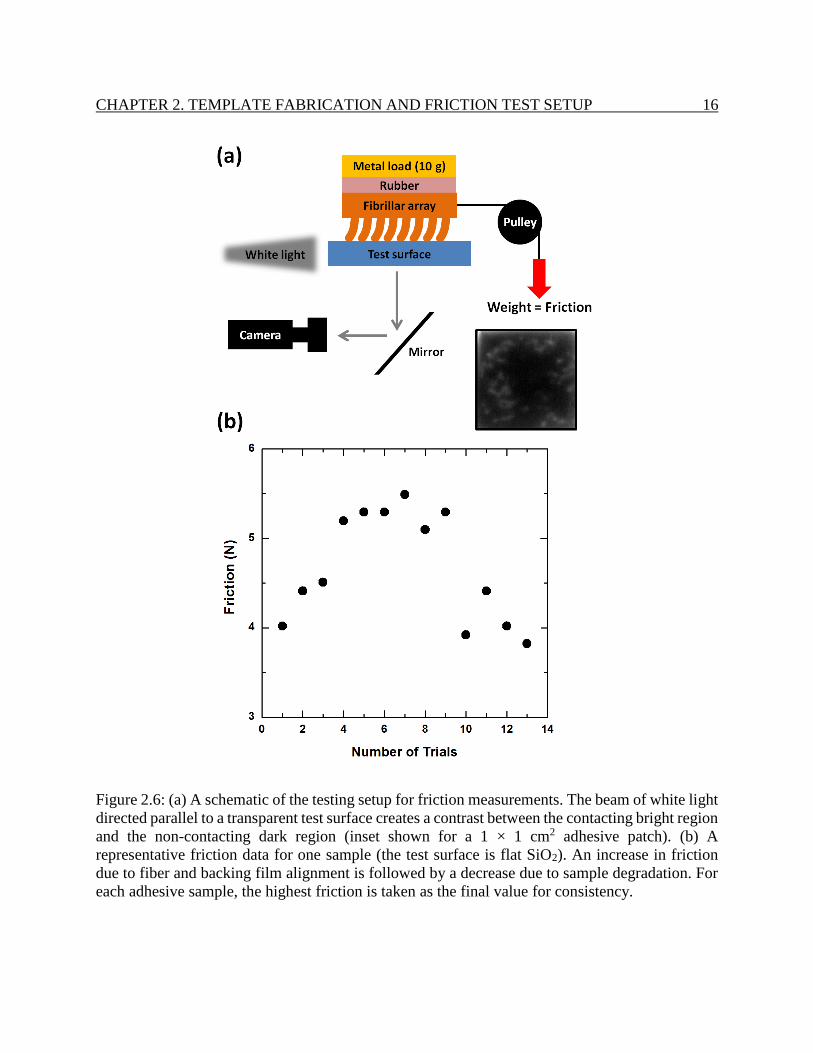
The schematic of the friction test setup is shown in Figure 2.6a. A 1 × 1 cm2 fibrillar array film
is brought in contact with the counter-surface with a rubber pad and a small normal load (10 g) on
top. The purpose of the normal load is to ensure a consistent sample contact with the counter-
surface for each test cycle, so that variation of friction due to film contact is minimized. The soft
rubber layer helps distribute the load across the sample. After the sample is contacted, a shear load
is progressively applied using a standard pulley setup with loading weight, and the static friction
prior to detachment is measured and recorded. Thermoplastic adhesives typically exhibit training
effects during repeated cycles [31], where the fiber and the backing film align with the counter-
surface during shear loading. This often results in a gradual increase in friction over multiple
testing cycles. Each sample has a limited lifetime, and the initial increase in friction is followed by
a gradual decrease due to contamination and deterioration. A representative example of this
behavior is shown in Figure 2.6b, where a sample increased in friction from 4 to 5.5 N, then
decreased to 3.8 N over 13 testing cycles. For consistency, the maximum friction value obtained
is taken as the friction value of that particular sample. Each friction data presented is based on
measurements of at least 3 samples. To minimize contamination, the counter-surface is thoroughly
washed with acetone, and the fibers with isopropanol, between each trial. Unless otherwise noted,
Page 23
CHAPTER 2. TEMPLATE FABRICATION AND FRICTION TEST SETUP 16
Figure 2.6: (a) A schematic of the testing setup for friction measurements. The beam of white light
directed parallel to a transparent test surface creates a contrast between the contacting bright region
and the non-contacting dark region (inset shown for a 1 × 1 cm2 adhesive patch). (b) A
representative friction data for one sample (the test surface is flat SiO2). An increase in friction
due to fiber and backing film alignment is followed by a decrease due to sample degradation. For
each adhesive sample, the highest friction is taken as the final value for consistency.
Page 24
CHAPTER 2. TEMPLATE FABRICATION AND FRICTION TEST SETUP 17
the tests are performed in an ambient condition at 20 °C and 35% relative humidity.
The bottom portion of the setup (the white light, mirror, and camera) allows the observation of
regions where the film is in actual contact with the counter-surface. Referred to as the frustrated
total internal reflection method (FTIR), a beam of white light is directed parallel to a transparent
substrate [74]. In presence of only glass/air interface, the light travels parallel to the surface, but
when a glass/LDPE interface forms, the light is redirected to the normal direction, where a camera
can record the resulting contrast between the contacting bright region and the non-contacting dark
region. An example of this is shown in the inset of Figure 2.6a for a 1×1 cm2 patch.
Page 25
18
Chapter 3
Effect of fiber length and diameter on macroscale
friction
This chapter is reproduced with permission from: D. H. Lee, Y. Kim, R. S. Fearing, R.
Maboudian. Effect of fiber geometry on macroscale friction of ordered low-density polyethylene
nanofiber arrays. Langmuir 2011, 27, 11008-11016 <http://pubs.acs.org/articlesonrequest/AOR-
JyXIubdUfFwS7RPMqJG8>. Copyright 2011 American Chemical Society.
3.1 Background
For GSAs there are only a few experimental reports [32, 75-78] on the effect of basic
geometrical factors such as fiber diameter, length, and density on the macroscale adhesion and
friction behavior. As reviewed recently [7] the basic issue of geometrical effect remains unclear,
as there have been contradictory results regarding the effect of aspect ratio on the adhesion or
friction of fibrillar surfaces. A systematic study has been reported by Greiner et al. [75], where
increased adhesion for higher aspect ratio of cross-linked polydimethylsiloxane (PDMS)
microfibers was attributed to larger elastic dissipation during the pull-off process. However,
Glassmaker et al. [77] have shown that measured pull-off stresses of poly(vinyl-butyral) fibers
were nearly independent of fiber lengths, though the energy dissipation increased linearly with
increasing fiber length as expected due to the higher stored elastic strain energy in a single fiber.
In some cases, increasing aspect ratio was observed to decrease adhesion or friction. Burton et
al. [76] measured the pull-off forces of poly(methylmethacrylate) and polyurethane acrylate
nanofibers and reported lower adhesion for higher aspect ratio at various humidities. Zhao et al.
[78] have reported a decrease in adhesive strength with increasing height of multi-walled carbon
nanotube arrays which was attributed to the formation of canopy-like entangled surface layers as
MWCNT fibers become longer. In contrast, Qu et al [32]. have more recently demonstrated a
dramatic increase in adhesion and friction with increasing MWCNT fiber length. They have shown
shear-induced alignment of top-entangled MWCNT fibers, which became more significant with
increasing fiber length.
Page 26
CHAPTER 3. EFFECT OF FIBER LENGTH AND DIAMETER ON FRICTION 19
The goal of this chapter is to systematically investigate the effects of fiber geometrical factors,
namely length and diameter, on their friction characteristics and to provide a useful reference for
optimum conditions for high performance. To minimize complications from the substrates, smooth
glass is used as the counter-surface. It is demonstrated that macroscale friction of these ordered
nanofiber arrays is very sensitive to small changes in those parameter. A friction design map is
presented by modifying the adhesion map previously reported [79], and a good agreement with
experimental results is observed regarding the optimal geometry of the LDPE nanofibers.
3.2 Fabricated LDPE fiber arrays
As mentioned in Chapter 2, the fabrication method used allows precise control over the length
(L) and diameter of the fibers (D = 2R). For this geometrical study, the initially deposited spheres
are 1 m in diameter (corresponding to fiber center-to-center distance of 1 m), and the fiber
diameter and length are in the range of 0.2 m to 4.5 m and 400 – 900 nm, respectively. Figure
3.1 shows representative images of LDPE nanofibers with various diameters and lengths.
3.3 Fiber clumping
As shown in Figure 3.1, with increasing fiber length, some of nanofibers start bending and
contacting each other (referred to as the partial clumping regime, e.g., the third row for D ~ 600
nm); then all the nanofibers clump (all images on the 4th row) into bundles with further increasing
length (referred to as the clumping regime). For the fibers contacting at their tips, a simple equation
can be derived from Johnson-Kendall-Roberts theory of adhesion and elastic beam theory [80-82]:
3/13
W
ERL t
crit , (3.1)
where Lcrit is the maximum length before clumping, 2 the spacing between adjacent fibers, Rt the
radius of curvature of the fiber tip, E the Young modulus (~200 MPa for LDPE [83]), and W (the
adhesion energy of the fiber. The adhesion energy is twice the surface energy of LDPE (W = 2*γf
= 60 mJ/m2 for LDPE [67]). As shown in Figure 3.2a, experimentally observed values in this study
coincide reasonably well with the theoretical prediction, assuming that the tip radius of curvature
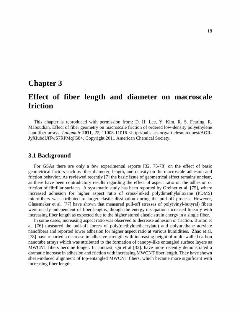
is equal to the fiber stock radius (Rt = R). This is a reasonable approximation supported by the
experimental observations shown in Figures 3.2b and c, where the tip-curvature of the nanofiber
is measured from the side view SEM image (Figure 3.2b and c). This clumping behavior will later
be discussed as a critical factor limiting friction performance of a fibrillar adhesive.
Page 27
CHAPTER 3. EFFECT OF FIBER LENGTH AND DIAMETER ON FRICTION 20
Figure 3.1: Representative SEM images of LDPE nanofiber arrays with increasing length down
the row for each fiber diameter. Fiber clumping is observed above a certain critical length. The
black outlines indicate the length at which the fibers exhibit the maximum friction for a given
diameter. Scale bar = 1 µm.
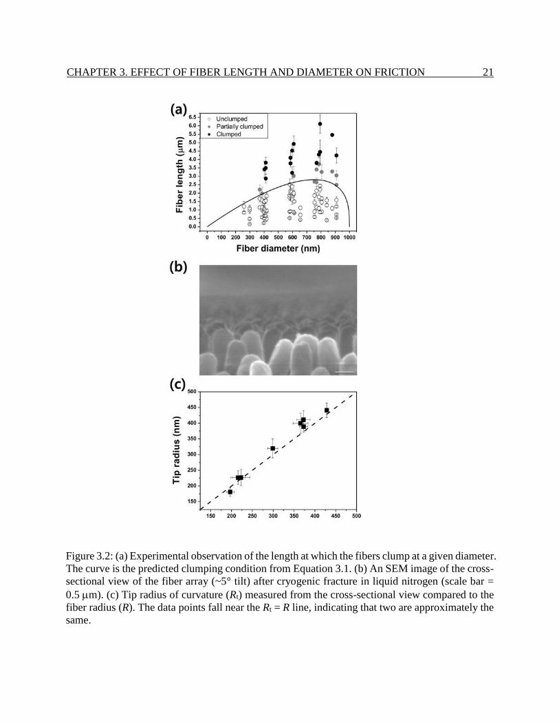
3.4 Macroscale friction of LDPE nanofiber arrays
By the method detailed in Section 2.5, macroscale friction of 1×1 cm2 fibrillar array film has
been measured for the wide range of length and diameter, and the result is plotted in Figure 3.3a
and b. At each diameter, a maximum friction force is observed with respect to the fiber length.
This maximum point increases with diameter up to D ~ 800 nm, then decreases for D ~ 900 nm,
indicating an optimum with respect to the diameter as well. The maximum friction observed (~6
N) is comparable to the adhesion of about 10 N for the same patch area of a natural gecko pad.
The next sections will explain why such optimal behavior is observed for the fiber length and
diameter, and how friction can be maximized by tuning the fiber geometry.
Page 28
CHAPTER 3. EFFECT OF FIBER LENGTH AND DIAMETER ON FRICTION 21
Figure 3.2: (a) Experimental observation of the length at which the fibers clump at a given diameter.
The curve is the predicted clumping condition from Equation 3.1. (b) An SEM image of the cross-
sectional view of the fiber array (~5° tilt) after cryogenic fracture in liquid nitrogen (scale bar =
0.5 m). (c) Tip radius of curvature (Rt) measured from the cross-sectional view compared to the
fiber radius (R). The data points fall near the Rt = R line, indicating that two are approximately the
same.
Page 29
CHAPTER 3. EFFECT OF FIBER LENGTH AND DIAMETER ON FRICTION 22
Figure 3.3: (a) Friction of LDPE nanofiber array (1 × 1 cm2 patch) with various fiber diamters and
lengths with fixed center-to-center distance of 1 µm. (b) The data set of D = 900 nm has been
plotted separately with that of D = 800 nm for clarity. For (a) and (b) the lines are guides to the
eyes, and the dotted circles indicate the points at which partial clumping is observed. (c) A
representative plot of apparent contact area % (apparent contact area/test area 100) with respect
to the fiber length (for D = 800 nm). While ~6 fold increase of friction force is observed, the
apparent contact fraction is not significantly altered between samples, typically 10 - 15% for all
cases.
Page 30
CHAPTER 3. EFFECT OF FIBER LENGTH AND DIAMETER ON FRICTION 23
Figure 3.4: The apparent contact area indicating the portion of the film which is in actual contact
with the glass from before being shear loaded (left) to just prior to being detached (right). The red
square outlines the sample area (approximately 1 × 1 cm2), and the contacting bright region is
indicated with red outlines.
3.5 Apparent contact area
Before relating the nano-scale geometry of fibers to the macroscale friction of the array, it is
important to note that not the entire film area is in contact with glass. Figure 3.4 shows the apparent
contact area measured by the FTIR method, and it is observed that the contact is not uniformly
distributed across the surface, but rather concentrated in the specific area with an irregular shape.
The bright zone indicates that the contacting region increases from the initial to final state with a
concomitant increase in brightness during the friction measurement.
Though non-contacting dark regions are clearly distinguished from contacting bright regions
by this method, detailed micro-scale information inside the contact region is unknown. For
example, the actual number of LDPE nanofibers in contact with the counter surface may be smaller
than that estimated from the area defined by the bright region. It is noted that any difference in
brightness may be influenced by the actual number of contacting nanofibers or by morphological
change in contacting nanofibers, e.g., from tip to side contact. Thus, bright region is referred to as
the apparent contact area. Despite the lack of detailed microscale information, it is useful for
friction analysis in macroscale to visualize how the nanofiber contact is confined within this
apparent contact area.
Since the static friction force is determined by the state just prior to sliding, the apparent contact
area at this moment should be considered. It was found that this apparent contact fraction (fca =
apparent contact area / test area 100) was not significantly different between samples, typically
10 - 15% for the sample size of ~11 cm2 as shown in Figure 3.3c, which is similar with the
Page 31
CHAPTER 3. EFFECT OF FIBER LENGTH AND DIAMETER ON FRICTION 24
previous results for polypropylene fiber arrays (~11%) [84]. Distributions of each data point in
Figures 3.3a and b may reflect the variation in contact area for each test. Despite this distribution,
it is clear that the measured friction forces are strongly correlated with the nanofiber geometry.
3.6 Friction prediction and dependence on fiber diameter from JKR
model
In general, friction between surfaces can be modelled as the sum of two components as follows,
NFAF , (3.2)
where τ is the shear strength coefficient, A is the real area of contact, µ the Coulomb friction
coefficient, and FN the normal load [85]. The first term is the area-dependent adhesive contribution
to friction, while the latter is the load-dependent mechanical friction. In the limit that adhesion
between two surfaces can be neglected (as is the case with many macroscale contact with few
contact points), the equation reduces to the familiar linear relationship between the applied normal
load and friction. In gecko adhesion, however, the adhesive term is likely to be the dominant
contribution, due to the increased number of contact points. Applying the equation to a single fiber:
fN,ff FAF , (3.3)
where Ff, Af, and FN,f are the friction, tip contact area, and normal load per fiber. The shear
coefficient for LDPE-glass interface is 6 MPa [86]. The tip contact area can be estimated from the
well-known Johnson-Kendall-Roberts (JKR) equation [80]:
3/2
2
ttfN,tfN,t
2
f 3634
13
WRRWFWRF
E
RA
. (3.4)
All the variables have been previously defined except the Poisson ratio (v ~ 0.4 for LDPE [87]),
and the adhesion energy is W = 2(γf*γg)1/2, where the surface energies of the fiber (γf) and glass (γg)
are ~30 and ~100 mJ/m2, respectively [67, 68]. The second coefficient, µ , between LDPE and glass
is 0.3 [86]. A 10 g (0.1 N) of normal load is applied to the 1 × 1 cm2 patch, which contains
approximately 108 fibers. However, only about 15% of film is in contact with glass, which
corresponds to 7 nN of normal load per fiber. With all the terms now known, the adhesion
contribution to friction is calculated to be 75 – 220 nN for the range of diameters tested (400 – 900
nm). Corresponding macroscale friction range is 1.1 – 3.2 N, which is a reasonable range of values
compared to those observed in Figure 3.3a and b, although somewhat underestimated. The load- aaa
Page 32
CHAPTER 3. EFFECT OF FIBER LENGTH AND DIAMETER ON FRICTION 25
Figure 3.5: An SEM image of LDPE nanofibers after being friction tested. In some cases where
the nanofiber array exhibited high friction, the fibers in the contacting region show permanent
slating deformation with plastic yielding at the tip, indicating where the contact has been made
(dotted circle). The arrow indicates the relative direction of shearing (by glass) at the tip. Scale bar
= 1 m.
dependent friction is only about 2 nN per fiber (0.03 N for the sample), confirming that this term
contributes little to the overall friction of LDPE fibrillar adhesive.
Although the contact area analysis based on JKR theory gives a reasonable approximation as
discussed above, it does not explain the complex behavior of friction forces depending on fiber
diameter and length. Specifically, any variation in friction forces according to fiber length cannot
be explained. Intuitively, lateral flexibility of the nanofibers may play significant role in friction,
e.g., through further increase in contact area or fiber alignment during friction measurement. As
mentioned, elastic dissipation and side-contact models have been typically considered for
explaining changes in adhesion and friction with respect to fiber length (or more generally, aspect
ratio). Elastic dissipation theory considers trapped and dissipated energy induced by fiber
stretching in normal direction during the pull-off from the substrate [75, 77]. Thus, this theory
explains only the effect of fiber geometry on normal adhesion, and is not directly applicable to
frictional properties. On the other hand, side-contact models describe bending of sufficiently long
fibers, which brings them into a stable side-contact with the opposing surface when adhesion is
high enough to exceed the elastic bending forces [84, 88]. However, the SEM image of the fibers
after friction testing (Figure 3.5) shows nanoscale plastic yielding at the fiber tips, which clearly
indicates that the fiber contact is restricted to the tip. An approach developed to estimate the side
contact length [84] predicts no side contact for all the geometries of LDPE nanofibers tested in
Page 33
CHAPTER 3. EFFECT OF FIBER LENGTH AND DIAMETER ON FRICTION 26
this study, which further supports that there is no side-contact induced by large bending of LDPE
nanofibers.
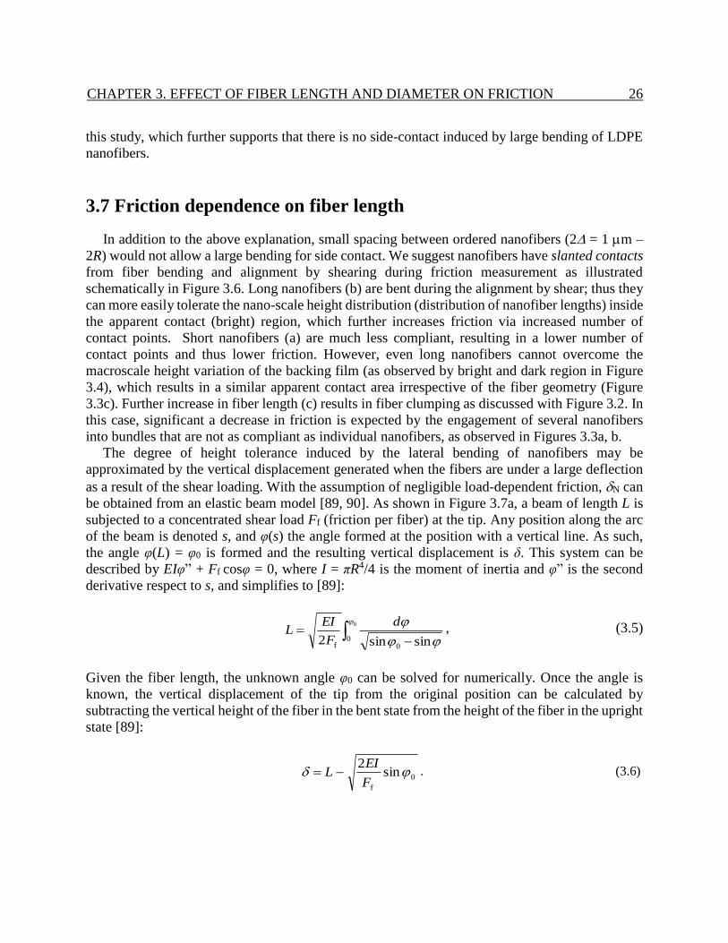
3.7 Friction dependence on fiber length
In addition to the above explanation, small spacing between ordered nanofibers (2 = 1 m –
2R) would not allow a large bending for side contact. We suggest nanofibers have slanted contacts
from fiber bending and alignment by shearing during friction measurement as illustrated
schematically in Figure 3.6. Long nanofibers (b) are bent during the alignment by shear; thus they
can more easily tolerate the nano-scale height distribution (distribution of nanofiber lengths) inside
the apparent contact (bright) region, which further increases friction via increased number of
contact points. Short nanofibers (a) are much less compliant, resulting in a lower number of
contact points and thus lower friction. However, even long nanofibers cannot overcome the
macroscale height variation of the backing film (as observed by bright and dark region in Figure
3.4), which results in a similar apparent contact area irrespective of the fiber geometry (Figure
3.3c). Further increase in fiber length (c) results in fiber clumping as discussed with Figure 3.2. In
this case, significant a decrease in friction is expected by the engagement of several nanofibers
into bundles that are not as compliant as individual nanofibers, as observed in Figures 3.3a, b.
The degree of height tolerance induced by the lateral bending of nanofibers may be
approximated by the vertical displacement generated when the fibers are under a large deflection
as a result of the shear loading. With the assumption of negligible load-dependent friction, N can
be obtained from an elastic beam model [89, 90]. As shown in Figure 3.7a, a beam of length L is
subjected to a concentrated shear load Ff (friction per fiber) at the tip. Any position along the arc
of the beam is denoted s, and φ(s) the angle formed at the position with a vertical line. As such,
the angle φ(L) = φ0 is formed and the resulting vertical displacement is δ. This system can be
described by EIφ” + Ff cosφ = 0, where I = πR4/4 is the moment of inertia and φ” is the second
derivative respect to s, and simplifies to [89]:
0
00f sinsin2
d
F
EIL , (3.5)
Given the fiber length, the unknown angle φ0 can be solved for numerically. Once the angle is
known, the vertical displacement of the tip from the original position can be calculated by
subtracting the vertical height of the fiber in the bent state from the height of the fiber in the upright
state [89]:
0
f
sin2
F
EIL . (3.6)
Page 34
CHAPTER 3. EFFECT OF FIBER LENGTH AND DIAMETER ON FRICTION 27
Figure 3.6: An illustration of the possible contact morphologies of nanofibers during the shear
loading. (a) Within the contact portion of the film, short fibers are not flexible enough to adapt to
any surface roughness or height variation in the array. No fibers are in contact in the dark region.
(b) Long fibers can adapt better to increase the number of fibers in contact within the apparent
contact area to increase the friction, but still unable to overcome any macroscale variation in film.
(c) Clumping is detrimental to friction as the fibers lose flexibility and tips available for contact.
Page 35
CHAPTER 3. EFFECT OF FIBER LENGTH AND DIAMETER ON FRICTION 28
Figure 3.7: (a) A schematic showing the variables associated with the fiber bending. A shear
force loaded at the tip (Ff) creates a vertical displacement (δ) and creates the angle φ along the
arc s. (b) A comparison of δ with respect to the applied load for long (3.3 µm, close to the
maximum friction) and short (1 µm) fiber with D = 800 nm.
Figure 3.7b is a representative result for D ~ 800 nm, which compares for short (1 µm) and
long (3.3 µm) fibers when the applied force increases up to the theoretical friction force (Ff). Long
nanofibers can have a significant normal displacement up to ~50 nm. Structural hindrance imposed
by the fiber gap may make this value smaller, e.g., ~10 nm if the lower limit of is assumed to be
given at a corresponding lateral displacement (L) of 2 (i.e., at L = 200 nm with D = 800 nm).
Meanwhile, short nanofibers have only negligible value up to ~0.1 nm (corresponding L ~ 15
nm). Note that the long nanofiber has much greater values than the short one by 2-3 orders of
magnitude. While short nanofiber array detaches from the substrate by further increasing the load
(i.e., exceeding the sum of the theoretical friction of all fibers in contact), long nanofiber array are
able to withstand higher load by increased contact from neighboring nanofibers (which were not
in contact previously) induced by this height toleration. Our previous discussion based on the
schematics in Figure 3.6 is well supported by this explanation. This also suggests the increased
brightness in the apparent contact area during friction measurement (Figure 3.4) is due to the
increased number of contacting nanofibers. While this analysis is a helpful aid in relating the
observed macroscale friction behavior to the mechanical behavior of the nanofibers, it is important
to note its limitation. For example, the contact deformation of the fibers is accompanied by some
degree of plastic yielding in addition to the elastic bending, which is not taken into account by the
simple elastic model.
Page 36
CHAPTER 3. EFFECT OF FIBER LENGTH AND DIAMETER ON FRICTION 29
3.8 Optimum fiber length
As indicated in Figure 3.1 with black and Figure 3.3a and b with dotted circles, the fiber length
at maximum friction (Lmax) for a given fiber diameter is close to the fiber clumping condition (Lcrit).
As can be envisioned from Figure 3.6c, fiber clumping is detrimental to friction as also
experimentally observed – maximum friction values for D ~ 400 and ~600 nm are obtained for the
unclumped structures just prior to clumping (Figure 3.3a). However, it is interesting to note that
the maximum friction forces for D ~ 800 and ~900 nm are observed for a partially clumped
structure (Figure 3.3b). The morphology difference between unclumped and partially clumped
nanofibers becomes less distinguishable as the diameter increases. Due to the narrow spacing
between thick nanofibers, partially clumped nanofibers of large diameter are touching the
neighboring fibers with only a small deflection, and many of the nanofiber tips are still individually
exposed to contact the opposing surface (Figure 3.1, third row images for D ~ 800, 900 nm), which
is not the case for smaller diameter fibers (Figure 3.1, third and fourth row images for D ~ 400,
600 nm). Since thick nanofibers are not as readily bent as thin nanofibers, increasing the fiber
length into a slightly clumped state may still be helpful to obtain higher friction by achieving more
compliance for bending to further tolerate the height distribution and maximize the number of
contacts. Further clumping into the bundled structure with increasing length causes drastic
decrease in the fiber compliance, and friction decreases as observed.
3.9 Optimum fiber diameter
As seen in Figures 3.3a and b, friction forces at Lmax increase with diameter up to ~800 nm, but
decrease for ~900 nm. This is contradictory to JKR analysis which predicts increased friction for
larger diameter. This can be understood by extending our previous explanation based on fiber
bending and height tolerance: though larger fiber diameter increases the tip-contact area, it will
concomitantly decrease the gaps between fibers, which results in geometrical hindrance for lateral
fiber bending with enhanced tendency for clumping. Thus, decreased friction for D~900 nm can
be attributed to the reduced height tolerance due to restricted lateral bending of nanofibers.
Based on our results in this study, it is found that the optimum geometry of LDPE nanofiber
arrays for macroscale friction is D ~ 800 nm and L ~ 3 m with slight clumping, representing a
compromise between the tip contact area and the fiber compliance. It should be noted that this
structure is optimal for the specific case of having a flat glass as the counter-surface. The optimum
geometry could be different for rough surfaces for example, possibly with a smaller diameter and
larger spacing to tolerate a wider height distribution of the rough substrates.
Page 37
CHAPTER 3. EFFECT OF FIBER LENGTH AND DIAMETER ON FRICTION 30
3.10 Comparison with theoretical friction design map
Spolenak et al. [79] have proposed theoretical adhesion design maps for GSAs by considering
conditions that limit the adhesive performance, such as fiber fracture, ideal contact strength, fiber
clumping, and surface adaptability. The design map quantifies these criteria with respect to the
fiber radius (R) and the material modulus (E), so that a failure of fibrillar adhesive can be avoided
with proper geometrical and material considerations. It would be useful to see where the nanofibers
in this study are located in the design map. For this, a friction design map was developed by
modifying the equations used in Ref. 78 so that friction can be taken into account instead of normal
adhesion. The development of a friction design map by modifying the criteria from the adhesion
map is as follows.
- Fiber fracture
Fibrillar adhesive can fail by fiber fracture, when the applied stress on the fiber exceeds the fracture
strength of the material. The friction stress exerted on a single fiber (f) can be expressed as:
thf,
3/222
22
f
2
ff
2
)1(9
E
WR
RR
A
R
F , (3.7)
where the friction force (Ff) is the adhesive friction from Equation 3.3 at zero normal load and σf,th
is the theoretical fracture strength of the fiber based on the fiber radius (R). If the bulk shear
strength is approximated to be similar with tensile strength (~E/10), the above condition is
rearranged as:
2
)1(910 2
2/5
2/32/3
fracture
W
ER . (3.8)
- Ideal contact strength
An adhesive contact cannot be stronger than its ideal contact strength. Since the stress concentrated
on the actual contact area is considered as the ideal contact strength (σc), the limiting condition
simply reduces to the maximum allowed as:
b
W
A
A
A
Fc thc,
f
f
f
f
, (3.9)
and thus:
Page 38
CHAPTER 3. EFFECT OF FIBER LENGTH AND DIAMETER ON FRICTION 31
b
W , (3.10)
where b is the characteristic length of surface interaction. The above condition sets a maximum
parameter value that can be used for , which is well above typical values [86], for example, W
/ b (0.1 N/m) / (2 10-10m) = 500 MPa.
- Fiber clumping
As discussed in Section 3.3, adhesive can fail when a significant number of fibers clump into
groups. Equation 3.1 is used for the clumping condition, which is rearranged into
E
WR
N
3
clumping
8
4
1
, (3.11)
where N is the fiber number density (~108/cm2) and = L/2R is the aspect ratio. It is noted that
the number density is used instead of the area fraction used in the previous study [79]. Since the
number of fibers per unit area is fixed with the center-to-center distance of ~1 m (area fraction is
changed with respect to fiber diameter), the number density is used for comparing the nanofiber
geometry.
- Adaptability
The reduced material stiffness due to the fiber elements has been described as the effective
modulus [16], which is closely related to the ability of the fibers to conform to surfaces for adhesive
contact. The effective elastic modulus (Eeff) for vertical fibers can be expressed as:
2
2
4
RCEE N
eff , (3.12)
where C is a geometrical factor (typically ~10) [16]. The adaptability condition becomes:
N
2
efftyadaptabili
4
CE
ER . (3.13)
Eeff needs to be arbitrarily chosen to ensure the contact adaptability, which will depend on the
surface roughness.
Page 39
CHAPTER 3. EFFECT OF FIBER LENGTH AND DIAMETER ON FRICTION 32
It is noted that apparent contact strength (app, this is the strength of the adhesive for a given
patch area) increases with increasing fiber diameter in this study under fixed fiber number density,
different from the previous report [79] where larger diameter fibers mean lower number density
under fixed area fraction. app can be written as:
3/2
22
N
2
fN
app
f
2
)1(9
E
WRR
A
Fapp
, (3.14)
which gives R as the following form:
(3.15)
The friction design map can be obtained by drawing Equations 3.8, 3.11, and 3.13 with a set of
apparent contact strength values from Equation 3.15. Figure 3.8 shows the friction design maps
for three different aspect ratios. For this design map, Eeff was set at 5 MPa based on the estimated
Eeff values from Equation 3.12 which are 1 – 10 MPa at maximum friction condition (L = Lmax)
corresponding to different diameter fibers. In Figure 3.8a, for a low aspect ratio ( = 1), it can be
seen that most of short nanofibers are out of the optimum region limited by the surface adaptability
(R should be less than ~100 nm to be in the optimum region). This indicates that less stiff material
than E ~ 200 MPa is desired to ensure the contact for low aspect ratio geometry. For higher aspect
ratio at = 4 (a typical value at L = Lmax) in Figure 3.8b, most diameters are within the optimum
region while achieving a maximum friction stress up to ~200 kPa by increasing the diameter to
~700 nm. This is quite similar to the experimental values, that is, the friction stress for the actual
contact friction of 15% is ~5 N/0.15 cm2 ~ 300 kPa. Further increasing the diameter along the E =
200 MPa line is limited by the fiber clumping condition. This indicates that the design map in
Figure 3.8b also predicts the existence of optimal diameter at ~700 nm according to the fiber
clumping condition. Further increasing aspect ratio ( = 7) results in exclusion of all nanofiber
geometry out of the optimum region by the clumping limit, which is reflected by experimental
observation that friction decreases for clumped nanofiber bundles.
As discussed above, experimental results show that a slightly higher aspect ratio above the
clumping condition, i.e., partial clumping, is allowed to achieve higher friction for larger diameters.
This may indicate that the clumping limit needs to be less strict, allowing some range rather than
a fixed value. For example, if the red line (clumping limit line) in Figure 3.8b is allowed to slightly
shift upwards, increasing fiber diameter (along the E = 200 MPa line) to achieve higher friction is
bound by the surface adaptability limit rather than the clumping limit, as experimentally shown by
partially clumped structures exhibiting maximum friction forces (D ~ 800, 900 nm). Although the
friction design map in Figure 3.8 is based on simplified models, it successfully describes the
optimum geometry of LDPE nanofibers observed, and thus appears useful as a design guide.
.)1(9
24/32/1
2
N
app
W
ER
Page 40
CHAPTER 3. EFFECT OF FIBER LENGTH AND DIAMETER ON FRICTION 33
Figure 3.8: Friction design maps for LDPE nanofibers for three different aspect ratios ( = 1, 4, 7).
Eeff = 5 MPa was chosen for the surface adaptability limit. Shaded regions enclosed by three lines
(gray: fiber fracture limit, red: fiber clumping limit, blue: adaptability limit) in each figure define
the optimum design area to achieve at least 10 kPa of friction stress. Dashed line indicates E = 200
MPa. Dotted circles indicate the experimental region in this study (fiber radius, R ranges from 200
to 450 nm along the E = 200 MPa line).
Page 41
CHAPTER 3. EFFECT OF FIBER LENGTH AND DIAMETER ON FRICTION 34
3.11 Summary
This chapter examined the effect of two basic geometrical parameters of fibers, length and
diameter, on macroscale friction of a fibrillar array. The experimentally observed dependence of
friction on the two parameters was explained by simple JKR and elastic beam models, which
indicated that increasing diameter increased available tip contact area, while increasing length
facilitated the fibers to contact counter-surface by increasing compliance. Because fiber clumping
limits the aspect ratio, the optimum geometry for macroscale friction against a flat glass substrate
was found at D ~ 800 nm and L ~ 3 m with slight clumping, which represents the optimum
compromise between the tip contact area and compliance. A friction design map was developed
based on the adhesion map previously reported, and the predicted optimum region marked on this
map was found to be in a good agreement with the experimental observation.
Page 42
35
Chapter 4
Effect of counter-substrate surface energy
This chapter is reproduced with permission from: Y. Kim, F. Limanto, D. H. Lee, R. S. Fearing,
R. Maboudian. Role of counter-substrate surface energy in macroscale friction of nanofiber arrays.
Langmuir 2012, 28, 2922-2927 <http://pubs.acs.org/articlesonrequest/AOR-8mRysJmZEiGJ5
335qbxK>. Copyright 2012 American Chemical Society.
4.1 Background
As briefly introduced in Section 1.4, one of the limitations faced by current GSAs is that they
have mostly been tested on smooth glass, which is particularly suitable for high adhesion and
friction due to its high surface energy. Since it is critical for GSAs to perform on a wide variety of
surfaces as the natural gecko foot does, the role of counter-substrate surface energy in adhesion
and friction remains an important issue. Only a few experimental studies have compared adhesion
or friction of fibrillar surface against substrates with different surface energies. Autumn et al. [2]
reported similar shear stress of a gecko seta on hydrophilic oxidized Si and hydrophobic GaAs
surface, which they indicated as an evidence that capillary force does not play a significant role in
fiber adhesion. Huber et al. [91] reported significantly higher pull-off force for an individual gecko
spatula against glass in comparison to silicon wafer treated with hydrophobic monolayer at various
relative humidities, and concluded that the pull-off force is controlled by short-range forces with
capillarity contribution due to adsorbed water layer. However, Puthoff et al. [92] later reported
that the material property change of the foot-hairs due to humidity may be responsible for the
change in the observed adhesion, rather than any significant capillarity contribution. Ge et al. [93]
showed that for their carbon nanotube-based synthetic adhesive, shear force was similar against
substrates with varying surface energies, but the peel-off strength was correlated with surface
energies.
While it is difficult to directly compare such experiments due to variations in the adhesive
design and testing method, it seems that the quantitative role of counter-substrate surface energy
on the performance of GSA’s is unclear. This chapter provides some insights on this issue by
testing the LDPE fibrillar adhesive against substrates with a wide range of surface energies. Glass
Page 43
EFFECT OF COUNTER-SUBSTRATE SURFACE ENERGY 36
Figure 4.1: Chemical structures of four self-assembled monolayer precursors used for modifying
glass. Fluorinated (FDTS), hydrocarbon (DTS), brominated (BUTS), and amine-terminated
molecules are chosen so that the exposed end (indicated by the circle) can exhibit a wide range of
surface energy. All coatings are performed by reaction in the liquid phase, where the silane end
attaches to the glass.
surfaces treated by commercially available self-assembled monolayer (SAM) with various
terminal groups are used as test substrates. Friction data are discussed in the context of simple
theoretical models relating the substrate surface energy to fibrillar friction.
4.2 Counter-substrate preparation
For a systematic study relating to the surface energy, the substrate must be modified chemically
without a significant change in the roughness and modulus. SAM deposition is appropriate since
a monolayer thin molecular coating can alter the surface energy drastically with minimal impact
on the surface morphology. As shown in Figure 4.1, a SAM precursor typically consists of an
attachment end that covalently bonds to a substrate (the trichloro- or triethoxysilane end), and an
exposed end responsible for altering the surface energy of the substrate (in red circles). For glass
(SiO2), common precursor molecules are long-chained silane molecules. Four precursors are
chosen to cover a wide range of surface energy: 1H,1H,2H,2H-perfluorodecyltrichlorosilane
(FDTS), n-decyltrichlorosilane (DTS), 11-bromoundecyltrichlorosilane (BUTS), and 11-
Page 44
EFFECT OF COUNTER-SUBSTRATE SURFACE ENERGY 37
Table 4.1: The terminal group, contact angle, and the reported surface energies [taken or deduced
from Refs. 94 and 95] of untreated glass and glass modified by 11-aminoundecyltrichlorosilane
(AUTS), 11-bromoundecyltrichlorosilane (BUTS, Gelest), N-decyltrichlorosilane (DTS),
1H,1H,2H,2H-perfluorodecyltrichlorosilane (FDTS).
Substrate Terminal
Group
Contact
Angle
Surface
Energy
(mJ/m2)
Untreated Glass SiO2 <10° 100
AUTS-treated -NH2 75° 45
BUTS-treated -Br 90° 30
DTS-treated -CH3 107° 25
FDTS-treated -CF3 112° 15
aminoundecyltriethoxysilane (AUTS). To minimize any difference between the treated substrates
other than the exposed functional group, all selected precursors have been chosen to have a similar
chain length (10 to 11 carbons).
The surface treatment procedure is as follows. Glass slides (Fisher Scientific) are successively
sonicated in acetone and isopropanol for 10 min each, then cleaned in boiling Piranha solution (3 :
1 ratio of 97% H2SO4 and 35% H2O2) for 30 min. The cleaned glass is submerged in a coating bath
containing the silane precursor and organic solvent in 1:1000 volume ratio (50 µL : 50 mL) in a
nitrogen environment with less than 5% relative humidity. The organic solvent used and the
reaction time varies depending on the precursor. 1H,1H,2H,2H-perfluorodecyltrichlorosilane
(Alpha Aesar) is deposited in 2,2,4-trimethylpentane (EMD) for 1 hr. n-decyltrichlorosilane
(Gelest) and 11-bromoundecyltrichlorosilane (Gelest) are deposited in toluene (Fisher Scientific)
for 2 hr and 1.5 hr, respectively. 11-aminoundecyltriethoxysilane (Gelest) is deposited in
chloroform (Fisher Scientific) for 1 hr. After the deposition step, the substrates are sonicated for
10 min in fresh baths of respective solvents, followed by another 10 min in isopropanol. Finally,
they are post-baked at 130 °C in ambient pressure for 30 min.
Water contact angle is a good indication of how well the surface has been modified by the
monolayers. Static contact angles have been measured with 3 µL drops of deionized water using a
tensiometer (Ramé-Hart Model 290). Table 4.1 summarizes the water contact angles of glass
substrates modified by monolayers with various terminal functional groups. A good agreement
with contact angles reported in the literature suggests that the glass surfaces have been successfully
modified with monolayers, and the surface energy values are those typically reported in the
literature [94, 95] for the corresponding exposed functional groups. Topographical measurements
Page 45
EFFECT OF COUNTER-SUBSTRATE SURFACE ENERGY 38
by atomic force microscope (Digital Instrument Nanoscope IIIa, measured over 10 × 10 µm2 area)
showed that all treated substrates had root mean squared roughness between 1 - 2 nm, which is in
the range of roughness of the untreated glass surface, indicating that negligible change in substrate
roughness occurred by the SAM treatment.
4.3 Friction and surface energy of counter-substrate
The friction of LDPE fiber array against the SAM-treated surfaces has been measured by the
method presented in Section 2.5. The geometrical parameters of the array are fixed at D (diameter)
= 2R = 600 nm, L (length) = 2.5 µm, and the center-to-center distance of 1 µm, corresponding to
~1.0×10⁸ fibers/cm2. Figure 2a shows static friction of LDPE nanofiber arrays on the five
substrates of varying surface energies. The samples show high friction (~9 N) on untreated glass.
The significant improvement of friction on the untreated glass in comparison to the previous set
of data in Chapter 3 is likely due to improvement in fabrication procedure, in particular peeling
the polycarbonate template off the silicon template, rather than dissolving the silicon template with
possible damage to the polycarbonate film. Only a minor drop in friction (to ~8.5 N) is observed
on AUTS-treated glass despite the large change in the observed contact angle of the substrate.
However, a drastic drop in friction is observed for even lower surface energies, leading to a poor
performance on hydrocarbon (DTS) and fluorocarbon (FDTS) monolayers. While the friction
values on these two surfaces are quite similar, FDTS surface seems to exhibit a slightly higher
friction. AFM-based sliding friction measurements have reported higher values against
fluorocarbon monolayer than against hydrocarbon monolayer [96]. Similar phenomena may be
occurring in our case with some of the fibers sliding against glass. Figure 4.2b shows the
corresponding apparent contact fraction of the ~1 × 1 cm2 just prior to sliding, simultaneously
observed during the friction measurements. As shown, the apparent contact fraction does not
deviate significantly between substrates from the average value of ~17%, and therefore cannot
account for the large change in friction.
One possible explanation of the observed disparity in friction is that the water meniscus formed
from the environment (RH ~ 35%) increases the interaction between the sample and high surface
energy, thus hydrophilic, substrates. It has already been suggested that humidity can play a
significant role in fibrillar adhesion, either from capillary effect [76, 91, 97] or change in
viscoelastic properties of the material [92]. In either case, increasing adhesion is expected with
increasing relative humidity. However, the same friction measurements repeated for hydrophilic
glass in a low humidity environment (RH < 5%), as shown in Figure 4.2c, resulted in similar
friction, indicating that the humidity effect in our case is not significant.
With insignificant capillarity contribution in the testing condition, the friction of a single fiber
can be estimated in the same manner as presented in Section 3.6:
fN,ff FAF , (4.1)
Page 46
EFFECT OF COUNTER-SUBSTRATE SURFACE ENERGY 39
Figure 4.2: a) Macroscale friction of 1 × 1 cm2 sample against substrates with various modified
surfaces. b) The apparent sample contact area simultaneously observed for the same substrates. c)
Friction of nanofiber array against hydrophilic glass substrate at two different humidities.
Page 47
EFFECT OF COUNTER-SUBSTRATE SURFACE ENERGY 40
where τ is the shear strength coefficient, Af the tip contact area, µ the Coulomb friction coefficient,
and FN,f the normal load per fiber. With ~17% apparent contact and assuming all fibers within this
area are in actual contact, the normal load per fiber is ~6 nN. Taking friction against glass as an
example, a typical value of τ = 6 MPa for LDPE [86] and Af = 0.023 µm2 predicted from JKR
contact mechanics [80] yields ~140 nN of contribution to friction from the first term. The value of
µ = 0.3 for LDPE [86] gives rise to only a small value of ~2 nN for the second term.
With negligible contribution from the load-dependent friction, the counter-substrate surface
energy can affect friction in two ways. At low normal loads, the JKR prediction of fiber tip contact
area (Equation 3.4) reduces to:
3/22
t
2
f2
)1(9
E
WRA
, (4.2)
where E (~200 MPa [83]) and v (~0.4 [87]) are Young’s modulus and the Poisson ratio of the
LDPE fibers, W the work of adhesion between LDPE and the substrate, and Rt (~300 nm) the
radius of curvature of the fiber tip. The work of adhesion can be approximated as W = 2(γfγs)1/2,
where γf (~35 mJ/m2 [67]) and γs are the surface energies of the fiber and the substrate, respectively
[65]. This indicates that the fiber tip contact area is proportional to γs1/3.
The interfacial shear strength (τ) itself is also directly proportional to W as suggested by the
Cobblestone model of interfacial friction [98], in the case of static friction. This results in roughly
Ff α γs5/6 overall dependence, predicting a nearly linear decrease in friction with decreasing
substrate surface energy. This corresponds to 30 to 140 nN of friction per fiber over the surface
energy values from 15 to 100 mJ/m2. However, while this simplified analysis explains the decrease
in friction due to the reduced adhesion between a single fiber and the substrate, it cannot fully
account for the observed macroscale behavior, specifically the sudden drastic reduction in friction
in a narrow range of surface energy. To give further insight as to why such a drop in performance
is observed, the assumption that all fibers within the apparent contact area are in actual contact,
should be revisited.
While all substrates showed similar fraction of bright region (~17%), the light intensity within
the contacting region showed drastically different behavior during testing. As shear load was
progressively added, substrates with low surface energies (e.g. DTS) showed only marginal
increase in intensity, while those with high surface energies (e.g. AUTS) showed a significant
increase. It is important to note that the contact fraction (~17 %) only represents the macroscale
contact determined primarily by the non-planarity of the backing film. The higher light intensity,
on the other hand, is attributed to increased degree of microscale contact (as more intimate
LDPE/Glass interface is formed to redirect more incident light from the parallel direction along
the interface to the normal direction observed by the camera), suggesting either more fibers coming
into contact within the contact fraction, or conformational change of individual fibers from tip-
contact to side-contact [74]. As mentioned, the fibers are not sufficiently long to make such a
Page 48
EFFECT OF COUNTER-SUBSTRATE SURFACE ENERGY 41
Figure 4.3: Increase in light intensity of contacting area observed during friction measurements.
While samples against all substrates showed ~17% apparent contact area prior to sliding, only the
ones exhibiting high friction showed a significant increase in intensity.
conformation change, so the increase in intensity is likely from increased number of fibers in
contact, rather than transition from tip-contact to side-contact.
In order to correlate the number of fibers in contact with the intensity of images obtained from
FTIR method, the images were first converted to 256 grayscale, then the difference in grayscale
values between the contacting region and the background region was calculated (ImageJ, version
1.43u). This allows the quantification of the relative change in intensity, I, from the initial state
(before any shear loading) to the final state (just prior to detachnment), defined by the ratio
Ifinal/Iinitial. The analysis has been performed for the samples corresponding to the data in 4.2a, and
the result is summarized in Figure 4.3, which shows that there is a strong correlation between the
light intensity of the contacting region and the friction of the nanofiber arrays. The sharp drop in
friction against lower surface energy substrates, which could not be fully accounted by simply
considering either the capillary effect or the adhesion energy based on the apparent contact area,
is suggested to be from dramatically decreased number of fibers in actual contact.
As described in Section 3.7, the number of fibers in contact is directly affected by the ability
for fibers to bend to overcome any fiber height variation from fabrication and/or the roughness in
the substrate to induce neighboring fibers into additional contact. Equations 3.5 and 3.6 can again
Page 49
EFFECT OF COUNTER-SUBSTRATE SURFACE ENERGY 42
Figure 4.4: The vertical displacement, δ, of a fiber induced by a range of friction values, Ff. The
corresponding surface energy of the substrates required for generating the friction is also shown,
based on the approximated γ5/6 dependence. The inset shows the cross-sectional image of the
nanofiber array (scale bar = 2 µm).
be applied to calculate vertical displacement caused by the shear loading. The dependence on
substrate surface energy is reflected in the term Ff, since the maximum loading allowed on each
fiber is limited by the adhesion between the fiber tip and the substrate. As given earlier, the range
for the counter-substrates tested here is 30 – 140 nN. Figure 4.4 shows the maximum displacement
possible for an individual fiber (D = 600 nm, L = 2.5 µm) over various maximum theoretical
friction forces determined by the surface energies. For lower values of surface energies, e.g., 15 -
25 mJ/m2 corresponding to the substrates that showed very low friction (FDTS- and DTS-treated
surfaces), the fibers are able to bend only several nanometers. With increasing adhesion between
the substrate and the fibers, significantly more bending occurs, up to nearly 100 nm.
In the previous chapter, the idea that the fiber bending allows increasing number of fibers to
come into contact has been used to explain why fiber length is a critical factor in macroscale
performance of fibrillar adhesives, where the fibers must be flexible enough to overcome the
variation in fiber height and/or any roughness of the substrate. This can be similarly applied to
Page 50
EFFECT OF COUNTER-SUBSTRATE SURFACE ENERGY 43
Figure 4.5: Schematic illustration of the suggested microscale contact morphologies during the
friction testing of nanofiber array against high- and low-surface energy substrates. Arrows indicate
the direction of loading, where the sizes qualitatively show the relative magnitudes of the
maximum load before sliding.
explain the critical role surface energy may play in attachment of fibrillar adhesives, where the
adhesion between the fiber and surface must be sufficient to result in bending that can allow
neighboring fibers to come into additional contact, as schematically depicted in Figure 4.5. For the
LDPE nanofibers tested in this study, the critical point above which this can happen seems to lie
between the surface energy range between ~20 - 40 mJ/m2 as observed in Figure 4.2a. From Figure
4.4, this would imply that fibers have to overcome roughly 10 - 20 nm in either the roughness of
the substrate or the height variation of the fibers. The counter-substrate topography was measured
with AFM to be nearly smooth (RMS ~ 1 - 2 nm) as previously mentioned. From the SEM side
view of the nanofiber array (Figure 4.4 - inset), the RMS variation in fiber height was estimated to
be ~30 nm. Thus, it seems that for the LDPE nanofibers in this study, sufficient adhesion from
high surface energy substrate was required to ensure the fibers bent enough to tolerate the variation
in height and lead to the large observed macroscale friction values. Finally, as suggested by the
elastic beam model used in the analysis, any change in parameters that decrease the rigidity of
fiber (i.e., smaller diameter, larger length, and lower modulus) may moderate the sudden reduction
in performance at lower surface energies.
4.4 Summary
In this chapter, we examined macroscale friction of nanofiber arrays against substrates of
varying surface energy. While the arrays exhibited high friction on high surface energy substrates,
they showed unexpectedly low performance against those with low surface energy. The drastic
reduction could be explained neither in terms of capillary effect nor by only considering the
reduced adhesion resulting from reduced surface energy. Simultaneous measurement of contact
area by reflected white light showed that while the apparent contact area stayed similar between
Page 51
EFFECT OF COUNTER-SUBSTRATE SURFACE ENERGY 44
all substrates, the intensity varied significantly, indicating that the number of fibers in actual
contact was very sensitive to substrate surface energy. By relating the friction per fiber predicted
from the JKR model to the vertical displacement of the fiber, it was suggested that the nanofibrillar
array could overcome their inherent height distribution only when the substrates had sufficient
surface energy to ensure effective engagement. This study shows that surface energy of
countersurface is an important criterion in gauging the performance of gecko-inspired adhesives.
Future design of versatile fibrillar adhesives should ensure attachment to substrates with widely
varying surface energies, which are likely to be encountered in practical applications. For example,
higher aspect ratio structures with hierarchy could cover a wider range of counter-substrate surface
energy via easier fiber bending even under weak interfacial adhesion.
Page 52
45
Chapter 5
Effect of counter-substrate roughness
This chapter is reproduced with permission from: Y. Kim, R. K. Claus, F. Limanto, R. S.
Fearing, R. Maboudian. Friction characteristics of polymeric nanofiber arrays against substrates
with tailored geometry. Langmuir 2013, 29, 8395-8401 <http://pubs.acs.org/articlesonrequest
/AOR-zasD6r7JwTvaZcEnujbF>. Copyright 2013 American Chemical Society.
5.1 Background
While many fibrillar adhesives perform well against smooth surfaces, their adhesion and
friction are drastically reduced with the introduction of surface roughness [18, 29, 47, 50, 64].
Since most surfaces encountered in practical applications are rough at various length scales,
understanding the interface between fibrillar and rough substrates is critical in rational design of
fibrillar adhesives. Only a limited number of studies have experimentally probed the effect of
roughness on fibrillar adhesion and friction. Studies of natural geckos show that the ability of the
animal to cling to an angled or inverted surface can exhibit a minimum [42] or maximum [99],
depending on whether the surface roughness scale allows for the penetration of nanoscale spatula
or microscale seta structures. Synthetic gecko adhesives have shown similar behavior with a
maximum pull-off strength [100] and friction force and normal adhesion after sliding [101], when
the roughness was compatible in scale with the fibers. Other studies, however, have shown
monotonic decrease in normal and shear adhesion with increasing roughness [18, 47, 64]. While
these studies suggest interesting and complex relationships between roughness and
adhesion/friction, the surfaces used had randomly rough features that are difficult to characterize
and compare. Although this is true of surfaces in real use situations, simplified model substrates
with defined patterns would aid in fundamental understanding of fibrillar contact against rough
surfaces. To this end, some studies have used microfabricated gratings to test adhesion or friction
on substrates with more well-defined features, where fibers are observed to deform to conform to
the substrate during normal loading [20], and the friction has shown to decrease with increasing
peak heights [29]. Incorporation of a structured backing more compatible with corrugation on the
counter-substrate has also been demonstrated to improve shear adhesion [50].
Page 53
EFFECT OF COUNTER-SUBSTRATE ROUGHNESS 46
Still, many factors that contribute to defining rough surfaces, e.g., spacing, height, and shape
of asperities, have not been studied in detail and further elucidation would help in design of gecko-
like adhesives that perform well on practical surfaces. In addition, most of the literature, in
particular studies that focus on the roughness effect [100, 101], have used soft elastomers (such as
PDMS with Young’s modulus of a few MPa or lower). Such materials can have large bulk
deformation to conform to surface features, which is not possible with harder polymers such as
polyethylene (Young’s modulus 100 MPa or higher). This chapter presents a systematic study of
how macroscale friction of polyethylene nanofibrillar surfaces is affected by various geometrical
factors of roughness, such as the height of the peaks, distance between the peaks, and the area
available for contact. A simple method utilizing colloidal lithography and silica evaporation is
used to fabricate rough substrates with independent control over those geometrical factors. This
allows us to examine the factors that allow synthetic fibrillar adhesives to adhere successfully to
some rough substrates and fail on others. Simple mechanical models are used to aid the
understanding of the observed friction behaviors.
5.2 Counter-substrate preparation
As described in Section 2.2, colloidal lithography provides a simple way to pattern a large area
with repeating patterns. This facilitates the preparation of a model rough substrate with well-
defined asperities with control over the geometrical parameters such as height, width, and spacing.
The overview of the procedure is shown in Figure 5.1. A base silica layer of 300 nm is first
evaporated on a Si wafer, and then the substrate is diced into a size large enough for friction testing
(larger than 1 × 1 cm2). Microspheres of various diameters (0.5 – 8 µm) are deposited, and an
additional layer of silica is evaporated. After the removal of spheres by sonication, the substrate is
left with silica peaks where the interstices of the sphere array allowed the penetration of the
additional evaporated layer.
As depicted in Figure 5.1 (bottom), the microsphere array would ideally be hexagonally close-
packed, leaving triangular peaks around the area where the spheres were originally deposited.
However, due to some unavoidable defects from monolayer assembly, some peaks merge and
deviate from hexagonal arrangement. Therefore, we nominally take the size of the spheres to be
the peak spacing. In this process, the diameter of the initially deposited spheres determines the
resulting distance or the spacing between the peaks (SP), and the duration of silica layer evaporation
over the spheres can be varied to control the height of the peaks (HP). As needed, the deposited
spheres can be reduced in size by oxygen plasma prior to silica evaporation to increase the
interstitial area between the spheres, which results in peaks with larger areas at the top. A
representative 3-D AFM topography is shown in Figure 5.2a, along with a line profile (Figure
5.2b). Figure 5.2c is a representative AFM image of the evaporated silica layer, revealing
nanoscale surface texture.
Page 54
EFFECT OF COUNTER-SUBSTRATE ROUGHNESS 47
Figure 5.1: Colloidal lithography to produce patterned rough counter-surface. A base silica layer
is first evaporated, then the second silica layer is deposited over the sphere array. The spheres are
removed by sonication. 3D views of steps (ii) and (iv) are shown below.
Page 55
EFFECT OF COUNTER-SUBSTRATE ROUGHNESS 48
Figure 5.2: (a) A representative 3-D AFM topography of a patterned surface (SP = 8 µm is the
initial size of the sphere, HP = 300 nm is the height of the evaporated silica). (b) A line profile
across the surface corresponding to the line drawn in (a). (c) AFM topography of the evaporated
silica layer with nanoscale roughness (RMS = 1.1 nm).
Page 56
EFFECT OF COUNTER-SUBSTRATE ROUGHNESS 49
5.3 Friction and roughness of counter-substrate – effect of peak
spacing and height
For the roughness study, fiber diameter (D) is fixed at 510 nm, and fibrillar arrays with two
different fiber lengths (L) are fabricated (1 µm and 2 µm). In Figure 5.3a, the macroscale friction
of a 1 × 1 cm2 LDPE fibrillar array patch (L = 2 µm) is plotted against the counter-surface peak
height, HP, for three peak spacings, SP = 0.5, 1, and 8 µm. The friction against the control flat
substrate is ~5 N, and is generally adversely affected with the introduction of roughness. However,
the decrease is more drastic when the peak spacing approaches the fiber diameter (0.51 µm), e.g.,
high friction (4 - 5 N) is maintained for HP = 30 nm for SP = 8 µm, but the same height of roughness
for SP = 0.5 µm reduces friction by a factor of roughly 10. This could indicate that as peaks on the
counter-surface are placed closer together, individual fibers have more difficulty penetrating to
contact the valleys, and the overall number of contacting fibers is reduced (since the area of the
peaks accounts for only about 15% of the projected area, a significant number of fibers must reach
down to valleys in order to ensure high macroscale friction). Studies on randomly rough surfaces
for natural gecko and synthetic fibers have observed a drop in adhesion or friction as the average
size of the counter-substrate features becomes smaller than the fiber diameter [99-101]. While we
also observe reduction of friction at small asperity spacing, the reduction is evident even for peak
spacing higher than the fiber diameter. It seems that as the number density of the peaks increases
with decreased spacing, the fibers are more likely to be obstructed from making proper contacts
with the valleys. We also do not observe increase in friction as the asperity spacing and the lateral
dimension of the fibers become similar. The studies using polydimethylsiloxane (PDMS) synthetic
fibers [100, 101] suggest an interlocking mechanism of fibers and asperities to explain the high
friction, and it is indicated that the low modulus of PDMS (~0.75 MPa) facilitates the penetration
and interlocking [101]. LDPE is typically over two orders of magnitude stiffer (~200 MPa) which
would make the interlocking mechanism more difficult.
It is interesting to note that the evaporated silica control sample has roughness on the length
scale of a few nanometers (Figure 4c, RMS = 1.1 nm, with average peak-to-valley height of 3 nm),
two orders of magnitude smaller than the smallest dimension of the fibers. While fiber penetration
into such small features would be impossible, high friction values obtained on these control
samples (which only have the inherent roughness from the evaporated silica) indicate that the
LDPE fiber tip can sufficiently deform when features become small enough. Similarly, the
adhesion behavior reported on natural gecko spatula indicated that the spatula structure can adapt
well to surfaces with low roughness [42].
The friction behavior on substrates with 8 µm-separated features also suggests there is a critical
peak height at which the friction rapidly drops, i.e., while high friction is maintained up to 75 nm
of feature height, a drastic decline is observed for the feature height of 150 nm and above. The
dotted line in Figure 5a indicates the approximate peak height (for 8 µm peak spacing) below
which the samples exhibit high friction.
In order for a sufficient number of fibers to contact the valleys in shear loading, it is plausible
that the fibers that first contact the top of the peaks have to bend to allow neighboring fibers to aaaaaaaaaaaaaaa
Page 57
EFFECT OF COUNTER-SUBSTRATE ROUGHNESS 50
Figure 5.3: (a) Macroscale friction of 1 × 1 cm2 array of 2 µm fibers on patterned surfaces with
varying peak heights, HP, and spacing, SP, as well as a control flat surface. For SP = 8 µm, high
friction is maintained up to HP = 75 nm but sharply drops afterwards, and the approximate
boundary is indicated by the dotted line. This drop is observed at lower peak heights as SP
approaches the fiber diameter. (b) Friction tests against the same surfaces using 1 µm fiber array.
Similar performance is observed on a flat surface, and decreasing SP again adversely affects
friction. In comparison to 2 µm fibers, drop in friction occurs at lower HP.
Page 58
EFFECT OF COUNTER-SUBSTRATE ROUGHNESS 51
contact the valley. Above a certain peak height, however, fibers may not have enough bending
compliance to accommodate the height difference. To test the suggested mechanism, fibers that
are roughly half as long (1 µm) are tested, with all other geometric parameters held constant.
Friction tests against the same set of patterned surfaces were done with the result plotted on Figure
5.3b. On the flat surface, the fibers of two lengths perform similarly, and the friction of shorter
fibers are also adversely affected as the peak spacing gets smaller. With respect to peak height,
however, it is evident that the shorter fibers begin to exhibit low friction at a lower height,
consistent with the mechanism above. Long fibers significantly outperform shorter ones at HP =
75 nm for SP = 8 µm, as well as at HP = 30 nm for SP = 1 µm. While there may be some convolution
of effects from reduced peak spacing for SP = 1 µm as explained above, the tests on SP = 8 µm
should only highlight the relationship between the fiber length and peak height (since SP is much
larger than fiber diameter D), and the results have been replotted in Figure 5.4 for more detailed
analysis.
Figure 5.4: Friction comparison of 1 µm (short) and 2 µm (long) fibers on rough surfaces with
varying peak height HP with peak separation SP fixed at 8 µm (1 × 1 cm2 samples). Performance
of shorter fibers is more adversely affected by roughness than that of longer fibers. The solid (red)
and dotted (black) lines are piecewise predictions of friction behavior based on the JKR model (I),
bending limitations from an elastic bending model (II), and calculated reduction in the number of
fibers in contact (III).
Page 59
EFFECT OF COUNTER-SUBSTRATE ROUGHNESS 52
As indicated in Figure 5.4, the data can be categorized into 3 regimes: high friction region where
a high number of fibers are in contact (I), a transition point at which the peak height becomes
larger than the adaptability limit of the fibers (II), and the low friction region where only a small
fraction of fibers are in contact, due to their inability to contact the valleys (III).
The calculated friction per fiber can subsequently be related to the vertical displacement of the
fiber by an elastica model for beam bending as a first-order approximation (Equation 3.5 and 3.6),
in the similar manner as before. For fibers 1 µm and 2 µm in length, the corresponding δ values
are calculated to be 2 and 60 nm, respectively, which serve as rough estimations for the deflection
limit of fibers based on the bending flexibility (vertical lines in Figure 5.4). For 2 µm fibers, the
simple model seems to be consistent with the experimentally observed drop in friction, although
somewhat underestimating where the drop occurs. The critical peak height is significantly
underestimated for the shorter fibers, probably due to the limitations of the simple model. Plastic
deformation may also provide additional vertical displacement, which would be more significant
for short fibers relative to their elastic bending. For a practical consideration, it is noted that while
increasing fiber length further would provide more bending compliance, it is limited by lateral
fiber clumping, at which point the clumped group loses much of its ability to adapt to surface
roughness.
Finally, the low friction behavior can be approximated by considering the reduced number of
fibers in contact as fibers are no longer able to contact the valleys. The peak areas account for only
about 15% of the total area, and thus, most of individual contact points are lost due to fibers’
bending limitations at the microscale. Another, less significant loss occurs at the macroscale,
where the contact reduction of patch from 20% to 15% is observed for low friction samples. With
these two factors, the macroscale friction is predicted to be reduced to 2.1 N × 0.15 × (0.15/0.2) =
0.24 N, shown as line III in Figure 5.4.
Despite the simplicity and limitations, this analysis predicts similar trends to the experimental
behavior and the analysis offers an explanation on how fibrillar arrays of varying fiber lengths can
perform similarly on a flat substrate, yet drastically different on a substrate with a certain peak
height (75 nm in our case).
5.4 Effect of peak area fraction
So far, the proposed explanations of observed friction behavior rely on the assumption that the
number of fibers in actual contact is the dominant factor in determining the macroscale friction.
To support this, counter-substrates were prepared with varied area fractions occupied by the peaks
of the features. This is achieved by plasma etching the spheres prior to silica evaporation of the
features, which increases the interstitial area between the spheres. The height of the peak is chosen
at 300 nm so that the fiber contact with the valley is unlikely, and therefore the peak area directly
corresponds to the local area available for intimate contact. The friction behavior is shown in
Figure 5.5 for 1 and 2 µm fibers against substrates with varying peak areas while maintaining the
spacing and height constant at 8 µm and 300 nm, respectively. The macroscale friction correlates aaaaaaaaaaaaaaaaaaaaaa
Page 60
EFFECT OF COUNTER-SUBSTRATE ROUGHNESS 53
Figure 5.5: Macroscale friction of nanofibrillar array against rough surfaces having different peak
area fraction for two fiber lengths, 1 and 2 µm. Increase in peak area available for fiber contact
increases macroscale friction for both cases. The dotted lines are linear fits to respective data.
reasonably well with the peak area fraction for both lengths, supporting that the ability of the 1×1
cm2 sample to adhere to the counter-surface is predominantly driven by the local area available for
fibers to contact. As the peak height is too large to adapt for fibers of either lengths, no apparent
advantage of long fibers is shown on these substrates.
5.5 Criteria for high friction performance on rough surface
Based on the friction tests of LDPE fibrillated surfaces against patterned counter-surfaces with
varying asperity peak spacing, height, and area, the macroscale friction behavior on rough surfaces
can be summarized with simple criteria with respect to those geometric parameters. On a nominally
flat substrate, most of the fibers can come into contact, and the nanoscale roughness can be
overcome by tip deformation (Figure 5.6-i). With introduction of surface roughness, fibrillar arrays
can maintain high macroscale friction (ii) until the roughness peak height reaches beyond the
bending compliance of the fibers, at which point friction drastically drops (iii). This effect is more
Page 61
EFFECT OF COUNTER-SUBSTRATE ROUGHNESS 54
Figure 5.6: Summary of observed behavior in fibrillar friction against patterned rough surfaces.
High friction is observed for nominally flat surface (i), when peak is sufficiently shallow and
spaced (ii), and with large peak area available for contact (vi). Increasing peak height (iii),
shortening fiber length (iv), and closing the gaps (v) lead to low friction.
Page 62
EFFECT OF COUNTER-SUBSTRATE ROUGHNESS 55
severe for shorter fibers due to higher stiffness (iv). Regardless of the peak height, poor friction
performance is observed as the distance between the peaks becomes smaller than the fiber diameter
and prevents penetration of fibers (v). Finally, it is confirmed that the local contact area
predominantly determines the macroscale friction behavior, as macroscale friction correlated well
with the peak area available for fiber contact (vi).
5.6 Summary
This chapter probed the friction behavior between fibrillar arrays and rough surfaces by
independently controlling several parameters important in characterizing a rough surface. While it
was evident that the real area in contact with the fibers determined the macroscale friction, high
friction was ensured on only the surface whose roughness features had lower height difference
than the vertical displacement allowed for individual fibers and had sufficient gap to allow
penetration of the fibers. Simple models pertaining to adhesion and bending mechanics of fibers
could be used to explain some of the observed behaviors. In spite of the 2 orders of magnitude
greater modulus of LDPE compared to PDMS used in previous roughness studies [100, 101], some
similarities can be seen in that friction performance can suffer from having surface roughness that
prevents proper fiber contact. However, due to using more regularly defined surfaces, we observe
a very distinct drop of an order of magnitude in friction that can be specifically attributed to various
dimensions of the asperity, as well as that of the fibers.
While the presented method provided a way to fabricate and characterize patterned rough
surfaces for testing gecko-like adhesive, real surfaces present more challenges as the asperities are
randomly distributed and often are hierarchical. Designing an adhesive surface as versatile as the
natural gecko pad would require incorporation of complex hierarchical fibers that would adapt to
a wide range of asperity sizes, density, and shapes. This study provides some insights on what the
important parameters are in designing such an adhesive, and may provide a useful guidance
especially in cases where the application is targeted towards a specific surface and the roughness
compatibility between the adhesive and the target surface is critical.
Page 63
56
Chapter 6
Fabrication of complex fiber designs
So far, we have examined various aspects of fibrillar friction using well-defined, vertically-
oriented cylindrical pillars. While the simple fiber geometry allows for application of simple
modelling and provides insights into fundamental aspects of GSA performance, its limitation was
clear in their failure to adhere strongly to rough or low-energy surfaces. This motivates more
complex fiber designs, some of which were covered in the introduction as part of the literature
survey. This chapter presents some alternative methods for fabrication of complex high-aspect-
ratio structures. Sections 6.1 and 6.2 are dedicated to controlling the morphology of SiNW etched
by metal-assisted chemical etching. Significance of further examining the etching condition and
the resulting structure is two-fold: 1) it leads to better control over the template geometry for
subsequent molding into GSA, and 2) SiNW have attracted great interest due to their novel
physical and chemical properties and potential applications in nanoelectronics [102, 103],
optoelectronics [104], thermoelectronics [105], sensing [106], and renewable energy devices [107].
Section 6.1 focuses on the ratio of HF/H2O2 concentrations which affects the porosity, tapering,
and clumping of the SiNWs, as well as effects of introducing small amount of electrolyte to the
solution. Section 6.2 presents a method to induce unidirectional tilting and curving of SiNW by
means of adding organic solvents to the etching bath.
Later sections provide new fabrication schemes for complex fiber designs. Hierarchical
structures are fabricated by a few different methods that place nanofibers on top of micro-sized
base pillars. Composite fibers are fabricated, where two different materials are used for the fiber
and the backing film. Finally, a method to precisely tune the tapering angle of micropillar is
presented. While most of these fabrication methods do not employ metal-assisted chemical etching,
they utilize other silicon etching and soft lithography techniques, and the methods may aid in the
future fabrication of even more complex fiber designs.
Page 64
CHAPTER 6. FABRICATION OF COMPLEX FIBER DESIGNS 57
6.1 Controlling porosity, clumping, and tapering of SiNWs formed by
metal-assisted chemical etching
This section contains material from the following publication with permission from the
contributing authors: D. H. Lee, Y. Kim, G. S. Doerk, I. Laboriante, R. Maboudian. Strategies for
controlling Si nanowire formation during Au-assisted electroless etching. J. Mater. Chem. 2011,
21, 10359-10363. <http:/dx.doi.org/10.1039/C1JM11164G>. Reproduced by permission of The
Royal Society of Chemistry (RSC).
As briefly overviewed in Chapter 2, SiNWs are formed by chemically etching silicon covered
by gold mesh film with regularly patterned holes. In this section we aim to examine several factors
that control the resulting morphology of SiNW, in particular with respect to the porosity, clumping
and tapering of the SiNWs. The substrate preparation method is similar to that described in 2.1 -
2.3, and for simplicity the nanowire diameter and spacing are fixed at 400 nm and 1 µm, while the
length is varied by the duration of etching. We first explore the effect of HF/H2O2 ratio on the
SiNW morphology as the etching progresses. The clumping and porosification phenomena are
explained in terms of hole diffusion mechanism. A novel method to regulate these phenomena by
introducing electrolyte to the solution is presented.
6.1.1 Effect of HF/H2O2 ratio
Figures 6.1 and 6.2 show the structural changes in SiNWs with respect to the HF/H2O2 ratio
during the Au-assisted electroless etching. The ratio of etching constituents are noted by the
volume of HF/H2O2/H2O. For example, 1.8/0.2/8.0 denotes an etching condition in which 1.8 mL
of HF, 0.2 mL H2O2, and 8.0 mL of deionized water are added for the total of approximately 10
mL of solution for a 1 × 1 cm2 chip. At high HF/H2O2 ratio (Figure 6.1), SiNWs are etched
vertically, increasing in length as etching progresses. With lowering ratio, slightly tapered SiNWs
are tip-clumped with large bending in Figures 6.1b and c, and even SiNWs with low aspect ratios
are bent and collapsed toward the bottom gold surface with more tapering (Figure 6.2). Based on
the observed dependence of the NW morphologies on the relative ratio of HF and H2O2, the results
in Figures 1 and 2 are categorized into three different etching regimes – regime I for vertical
(Figure 1a), regime II for hooked (Figure 1b, c), and regime III for ground collapsed (Figure 2)
shapes, as summarized in Table 1.
Page 65
CHAPTER 6. FABRICATION OF COMPLEX FIBER DESIGNS 58
Figure 6.1: Temporal evolution of SiNWs during electroless etching of Si(100) for different
HF/H2O2 ratios. HF/H2O2/H2O = (a) 1.8/0.2/8.0, (b) 1.5/0.5/8.0, and (c) 1.2/0.8/8.0. Each column
indicates the etching time – 10, 20, 30 min. While SiNWs grow vertically for low H2O2
concentration (Fig. 1a – regime I), tip-clumped shape with large bending (hooked) SiNWs are
observed for higher H2O2 concentration (Figs. 1 b, c - regime II). 45 tilt view, scale bar = 1 m.
Figure 6.2: SEM images of SiNWs with further increasing H2O2 concentration (HF/H2O2/H2O =
0.9/1.1/8.0, etching time = (a) 5, (b) 10 min). Short, highly tapered SiNWs are observed to collapse
toward the bottom surface (ground collapse, regime III). Broken fibers are observed as indicated
by yellow dot circle (etching time = 10 min). The etched surface becomes unstable and
inhomogeneous with significant film dewetting after 20 min. 45 tilt view, scale bar = 1 m.
Page 66
CHAPTER 6. FABRICATION OF COMPLEX FIBER DESIGNS 59
Table 6.1: Compositions of etching solutions used in this study with volume in mL and molar
concentration in mol/L with a total volume of 10 mL for each 1 × 1 cm2 chip.
Regime Volume (molar conc.)
Morphology HF H2O2
I 1.8 (5.0) 0.2 (0.2) vertical
II 1.5 (4.1) 0.5 (0.6)
hooked 1.2 (3.3) 0.8 (0.9)
III 0.9 (2.5) 1.1 (1.2) ground-collapsed
6.1.2 Nano-porosity in SiNWs
As seen in Figs. 6.1 and 6.2, SiNWs in regimes II and III exhibit a large bending (approaching
a 90° angle at the bending point) that is far outside the bounds of the linear elastic regime as shown
elsewhere for SiNW bending under mechanical load [108, 109]. If the strain due to bending is
expressed as r/Rc, with Rc being the bending radius, the estimated strain value (> 10%) is much
larger than the maximum fracture strain of SiNWs (~1 – 2%) [108].
A recent paper has reported the increased porosity of SiNWs with large bending produced by
metal-assisted electroless etching [110]. The high surface area and low density of nanoporous Si
make it prone to faster ambient and wet chemical oxidation than single Si crystals, and hence
susceptible to subsequent HF attack. To examine the porosity in the hooked SiNWs presented here,
these samples are immersed in HF solution after wet oxidation in aqua regia solution as shown in
Figure 6.3. Freshly etched SiNWs are predominantly unoxidized silicon, based on two facts: (1)
The surfaces of the freshly prepared SiNW arrays are hydrophobic (water contact angles on the
SiNW array surfaces are often larger than 140 depending on the aspect ratio of the SiNWs) and
(2) negligible changes are observed for hooked SiNWs when immersed in HF solution right after
electroless etching (Figure 6.3b). However, sharp nano-cone structures are generated when the
hooked SiNWs are exposed to the highly oxidizing conditions of aqua regia treatment, followed
by HF treatment (Figure 6.3c). This indicates that hooked SiNWs possess a large degree of porosity
between the tip-end and bending point.
6.1.3 Visualization of hole diffusion effects
As shown in Figure 6.1b, c and Figure 6.2, hooked and ground-collapsed SiNWs have tapered
shapes. A tapered shape with a decreasing diameter toward the tip is rationalized in terms of
increased side-wall etching with higher H2O2 concentration. Sidewall etching and formation of
tapered shapes in silicon nano- or micro-holes [111, 112] and SiNWs [113, 114] have been reported
Page 67
CHAPTER 6. FABRICATION OF COMPLEX FIBER DESIGNS 60
Figure 6.3: SEM images of SiNWs immersed in HF solution (30 min) after wet oxidation in aqua-
regia solution (15 min) (45 tilt view, scale bar = 1 m). Initial structures right after electroless
etching are shown in (a) and (d) for hooked (preparation condition in Fig. 6.1b) and vertical
(preparation condition in Fig. 6.1a), respectively. This oxidation/etching procedure caused
removal of clumped SiNWs from the bent part to tip-end resulting in the formation of Si nanocones
(c), while little change is observed for vertical SiNWs (e). For comparison, clumped SiNWs
immersed in HF solution without wet oxidation right after electroless etching process show
negligible change in SiNW structure (b). This result strongly suggests that hooked SiNWs have a
nanoporous structure distributed between the bent part and the tip-end.
Page 68
CHAPTER 6. FABRICATION OF COMPLEX FIBER DESIGNS 61
previously, and explained by considering either partial dissolution of the metal [112-115] or
enhanced hole diffusion toward sidewall [111, 112] (injected by H2O2, reaction 2.1 and 2.2) away
from the narrow interfacial region in contact with the metal. Partial dissolution of Au seems less
probable in this study due to its relatively high redox potential as discussed in a previous report,
[112] and thus the tapered shape of SiNWs observed here is attributed mainly to the enhanced hole
diffusion toward the sidewall of SiNWs under high H2O2 concentration. It has been reported that
oxidative dissolution of Si in HF solution is accompanied by the formation of a nanoporous Si
structure, which is enhanced when more holes are injected into Si [110-112, 116-121]. This would
consequently lead to the tapering of SiNWs after etching and dissolution of nano-porous region
[111, 112, 122, 123].
For low H2O2 concentration, most of injected holes are consumed by Si dissolution at Au/Si
interface, giving rise to the vertical shape (regime I). Increasing H2O2, that is, increasing the hole
injection, can induce deviated diffusion of unconsumed holes at Au/Si interface toward the
sidewall, which results in the tapered shape by significant etching of porous sidewall (regime II).
Further increasing H2O2 concentration causes more significant development of porous sidewall
relative to vertical etching, which gives shorter SiNWs with more tapering. This eventually
becomes ground-collapsed (regime III). Details on how the porous NWs is bent are still unknown
and remain an open question.
To further highlight the effect of hole diffusion towards the sidewalls, we explored ways to
visualize it by changing the etching regime in a serial fashion during the synthesis process. A
simple strategy is designed as follows: (i) preparation of vertical SiNWs from regime I, and (ii)
exposure to electroless etching in regime III where significant tapering is typically observed. If
isotropic etching or Au dissolution is dominant, a similar structure (vertical shape) with a smaller
diameter should be observed (case A in Figure 6.4a). On the other hand, if sidewall etching due to
lateral hole diffusion is dominant over isotropic etching in regime III, neck formation around a
height corresponding approximately to the hole diffusion length scale should be observed (case B
in Figure 6.4a). This idea was tested using larger diameter (~600 nm) SiNWs (Figure 6.4b) to
magnify the effect. As shown in Figure 6.4c, baseball bat-shaped SiNWs are generated with a
significant amount of neck formation. This strongly highlights the role of hole diffusion for
solutions with high H2O2 concentrations during the electroless etching process, and shows that it
is concentrated at the Au/Si interface with a limited diffusion length scale. A more realistic
situation would be the case where the hole diffusion toward sidewall is dominant with some
contribution from isotropic etching. Beyond the fundamental importance in gaining a more
complete understanding of the metal-assisted electroless etching process for Si nanostructure
formation, the practical implication of this experiment is that various Si nano-architectures may
be fabricated with a proper understanding of the etching mechanism.
6.1.4 Regulating etching rate and clumping by electrolytes
As previously discussed, Au is more electronegative than Si, so the silicon beneath Au becomes
more positively charged during the etching process. It may be expected that catalytic effect of Au
Page 69
CHAPTER 6. FABRICATION OF COMPLEX FIBER DESIGNS 62
Figure 6.4: (a) Schematic illustration of the effect of transitioning from regime (I) to (III) during
etching. As illustrated, if isotropic etching is dominant, neck formation would not be observed (A).
If significant sidewall hole diffusion occurs with a length scale of ~h, NWs with neck formation
would be observed as in (B). The results are shown in the SEM images – (b) vertical SiNWs (~600
nm diameter, grown in regime I (HF/H2O2/H2O (time) = 1.8/0.2/8.0 (20 min)), and (c) SiNWs with
neck formation prepared by immersing (b) into etching solution with high H2O2 concentration
(regime III, HF/H2O2/H2O (time) = 0.9/1.1/8.0 (5 min)), which highlights the role of hole diffusion
near the Si/Au interface.
Page 70
CHAPTER 6. FABRICATION OF COMPLEX FIBER DESIGNS 63
would be significantly altered with the addition of electrolytes due to screening by counterions. To
test this idea, a small amount of common electrolytes was added to the etching solution (regime I).
As shown in Figure 6.5a and b, a substantial decrease in the etch rate was observed – e.g., from
~10 µm/hr (without an electrolyte) to ~2 µm/hr by adding 10 mM of NaCl. As shown in Fig. 6.5c
and d, the etch rate further decreases with higher NaCl concentration, and other electrolytes such
as KCl and CaCl2 have a similar effect on the etch rate depending the total ion concentration. These
findings strongly support the above hypothesis that the Au surface is effectively screened by
counterions from excess electrolyte, which then leads to diminished hole current density at the
Au/Si interface. This result is an important finding that common electrolytes can be used as a
retardant for metal-assisted electroless etching.
To further study the effect of added electrolyte on SiNWs morphologies, a small amount of
NaCl was added to the etching solutions which correspond to bent and clumped shape. Figures
6.6a and b show SiNWs structures obtained by adding 10 mM NaCl into the etching solution used
in Figure 6.1b and c, i.e., HF/H2O2/H2O = 1.5/0.5/8.0 and 1.2/0.8/8.0, respectively. Striking
morphological difference is observed: vertical NWs with more tapered shape are formed instead
of the hooked shape previously observed in the absence of NaCl. Note that the SiNWs in Fig. 6.6
are shorter than those in Fig. 1 under the same etch time, indicating that the etching rate decreases
in NaCl-containing solution. As discussed earlier, under the etching solution of regime II and III,
the porous regions generated by hole diffusion is formed, giving rise to a tapered shape after
sidewall etching. Thus, more tapered shape with shorter length in Fig. 6 can be understood by
greater contribution from porous sidewall etching when the reaction time is extended at a slower
rate in the presence of electrolyte ions in solution. Under these conditions, SiNWs tend to be less
porous and would not be subjected to clumping, and in extreme cases, long, spear-like structure
are produced as shown in Fig. 6.6c.
6.1.5 Summary
Dramatic changes in SiNW morphology was demonstrated depending on the HF/H2O2 ratio.
The hooked SiNWs with large bending beyond linear elastic deformation possessed a nano-porous
structure distributed from the bending region to the tip-end during the etching process. This
phenomenon was dominated by the relative amount of H2O2 to HF, so that increasing H2O2 was
accompanied with more bending and tapering, eventually leading to the ground collapse of short,
highly tapered SiNWs. These structural transformations were attributed to the enhanced hole
diffusion towards SiNW sidewalls during the electroless etching process, which was made more
evident by the observation of the neck formation when transitioning to different etching regime
during the SiNW formation. A method was demonstrated for the conversion of hooked SiNWs
into sharp nanocone structures by simple oxidation and etching. Furthermore, SiNW tip-clumping
could be regulated by adding a small amount of NaCl, which is attributed to a reduced metal-
assisted etch rate resulting from electric screening of the charged Au surfaces. Common electrolyte
can also be used as a retardant for the metal-assisted electroless etching.
Page 71
CHAPTER 6. FABRICATION OF COMPLEX FIBER DESIGNS 64
Figure 6.5: SEM images of SiNWs prepared with etching solutions of HF/H2O2/H2O (time) =
1.8/0.2/8.0 (40 min, regime I) – (a) without NaCl, and (b) with NaCl (10 mM) (45 tilt view, scale
bar = 2 m). SiNW lengths were plotted against the etching time for different NaCl concentrations
(c), and for different electrolytes (d).
Page 72
CHAPTER 6. FABRICATION OF COMPLEX FIBER DESIGNS 65
Figure 6.6: SEM images of SiNWs prepared with NaCl-loaded (10 mM) etching solutions of
HF/H2O2/H2O (time) = (a) 1.2/0.8/8.0 (10 min) and (b) 1.5/0.5/8.0 (30 min). The SiNWs are
unclumped and tapered unlike the hooked structures observed without NaCl. (c) Extended etch
time of 60 min with etch solution in (b) results in a long, spear-like nanostructure (45 tilt view,
scale bar = 1 m).
Page 73
CHAPTER 6. FABRICATION OF COMPLEX FIBER DESIGNS 66
6.2 Controlling directionality and curvature of SiNWs by addition of
co-solvant
This section contains material from the following publication with permission from the
contributing authors: Y. Kim, A. Tsao, D. H. Lee, R. Maboudian. Solvent-induced formation of
unidirectionally curved and tilted Si nanowires during metal-assisted chemical etching. J. Mater.
Chem. C 2013, 1, 220-224. <http://dx.doi.org/10.1039/C2TC00041E>. Reproduced by permission
of The Royal Society of Chemistry (RSC).
In metal-assisted chemical etching, the reaction bath often contains wetting agent or co-solvent
(usually methanol or ethanol) as a practical means to improve the overall etching uniformity of the
samples. While the ratio of HF to the oxidizing agent is known to dramatically affect the porosity
and the crystallographic direction of the SiNWs [73], the effect of wetting agent in the resulting
morphology of SiNW formed by metal-assisted chemical etching has received limited attention
[124, 125]. Chiappini et al. [124] has reported that the inclusion of ethanol with HF and H2O2
slows down the etching rate and affects the porosity of the resulting morphology. The Si(100)
substrates etched with Ag nanoparticles obtained by electroless deposition formed solid or porous
vertically-aligned SiNWs, in some cases on top of a porous silicon layer, depending on the
concentration of ethanol and resistivity of the starting wafer. In a study of pore formation by Si
etching in HF/H2O2/ethanol mixture using thin Au film as the metal catalyst, Chen et al. [125]
observed that the etching rate is significantly decreased with increasing amount of ethanol.
This section examines the effect of the concentration and the type of co-solvent on the
morphology of SiNWs formed via colloidal lithography and metal-assisted chemical etching. The
study expands the concentration range of the conventional wetting agents (namely methanol and
ethanol), and also examines other solvents such as 2-propanol and acetonitrile whose effects have
not been specifically studied in metal-assisted chemical etching of Si. It is shown that inclusion of
co-solvent can influence the etching direction as well as the etching rate, resulting in the formation
of non-vertical SiNWs. In addition, the fabrication of unidirectionally slanted or curved SiNW
array over a large area (on the order of 50 cm2) is demonstrated, with control over the curvature of
the wires to produce SiNW arrays that are either tilted or curved in the same direction. Such non-
vertical arrays have shown to present some advantages over the typical vertically-aligned SiNWs,
for example in improved electrode contact with excellent anti-reflective properties for solar cells
[126]. The current methods for fabricating slanted SiNWs generally rely on the HF/oxidant ratio
of the etching bath [116, 127, 128] or the orientation of the starting wafer [126, 129, 130, 131]. As
such, this study presents a simple alternative to fabricate unidirectionally-aligned SiNW, either
slanted straight or curved, only by controlling the amount of co-solvent added in the etching bath.
6.2.1 Co-solvent and directionality of SiNWs
The SiNWs in this section is 400 nm in diameter, 500 nm in center-to-center spacing, and varies
in length depending on the etching condition and duration. They are fabricated in the similar
Page 74
CHAPTER 6. FABRICATION OF COMPLEX FIBER DESIGNS 67
manner as explained previously, and an additional amount of various organic solvent is added to
the etching bath prior to etching. As such, the bath contains HF (48%, EMD), H2O2 (35%, Fisher
Scientific), DI water (18 MΩ), and an additional solvent (methanol, ethanol, 2-propanol, or
acetonitrile, Fisher Scientific). For a 5 × 5 mm2 chip, the total volume of solution is 10 mL. The
amount of HF and oxidant (H2O2) are fixed at 2 and 1 mL, respectively, while the ratio of water
and co-solvent are varied. From here on, we denote the volume composition as the ratio HF : H2O2 :
water : co-solvent.
Figure 6.7a shows a representative scanning electron micrograph (SEM) of Si(100) substrate
exposed to etching bath containing only HF, H2O2, and water (i.e., HF : H2O2 : water:co-solvent
volume ratio of 2 : 1 : 7 : 0) for 10 min. Under this etching condition, highly clumped SiNWs are
observed. Such morphology coincides with increased porosity of the SiNWs at high concentrations
of H2O2 relative to HF. As discussed above, under these conditions the excessive amount of holes
injected into Si by the oxidizing agent can diffuse to the sidewalls of the SiNWs and create nano-
porous portion of wires that can clump. Nonetheless, the etching direction is vertical with respect
to the substrate, as can be seen from the unclumped base of the wires and the fact that the porous
top sections are bent to form groups with no particular orientation or alignment.
Upon a significant addition of methanol at concentrations higher than the ratio HF : H2O2 :
water : methanol = 2 : 1 : 4 : 3, formation of some non-vertical wires is observed, as shown in
Figure 6.7b (2 : 1 : 2 : 5 ratio is given as a representative condition at 20 min of etching). Clumping
is also no longer observed, suggesting that the porosity has been reduced even though the ratio of
H2O2 to HF is constant. Finally, a drastic reduction in the etch rate can be seen in comparing Figure
6.7a and b, i.e., while they are similar in length (~6 µm), the case without the co-solvent took only
half the time in the etching bath. Addition of ethanol also results in non-vertical wires, although
the amount required to induce the formation is found to be less (2 : 1 : 6 : 1).
Previous reports in the literature regarding the formation of slanted SiNWs are rather conflicting.
While many studies [126, 129, 130, 132, 133] report <100> is the favored etching direction (which
would suggest that non-vertical SiNWs only form on wafers with orientation other than (100)),
preferential etching towards other directions has also been reported on Si(100) substrate [116, 127].
Some have reported the etching simply follows the orientation of the starting wafer, always
resulting in the vertical etching direction [134, 135]. Other factors, such as the etching rate [127],
the geometry of the catalyst pattern [113], and diffusion rate of the reactants [136], have also shown
to be critical parameters in etching direction, further complicating the prediction of resulting
directionality of the SiNWs in metal-assisted chemical etching.
Nevertheless, consistent with the studies on ethanol-containing etching bath by Chiappini et al.
[124] and Chen et al. [125], the overall etching rate decreased with the increased concentration of
the co-solvent. As co-solvents typically have low surface tension, it is likely that locally at the
reaction sites, co-solvents are preferably wetted and limit the availability of reaction species HF
and H2O2, resulting in slower etching rates. It may be speculated that while the <100> direction is
often observed to be the preferred etching direction since the number of Si back-bonds that have
to be broken is the lowest [137], significant reduction of the etching rate may suppress the
Page 75
CHAPTER 6. FABRICATION OF COMPLEX FIBER DESIGNS 68
Figure 6.7: Scanning electron micrograph of SiNWs etched in solutions composed by volume of
a) HF : H2O2 : water = 2 : 1 : 7 for 10 min and b) HF : H2O2 : water : methanol = 2 : 1 : 2 : 5 for
20 min. With the addition of wetting agent, non-vertical wire formation is observed. Both scale
bars = 2 µm.
Page 76
CHAPTER 6. FABRICATION OF COMPLEX FIBER DESIGNS 69
vertical etching and allow etching towards other major crystallographic directions or some vector
combination of them. In fact, Chern et al. [116], in a study that correlated the HF to H2O2 ratio to
SiNW orientation resulting from Ag-assisted etching, has suggested that higher relative
concentration of HF can allow etching in directions other than <100>, as HF becomes more readily
available to remove the oxidized Si. Similar phenomenon may occur for our case if H2O2 is more
severely shielded from reaction sites by co-solvent than HF is, possibly due to the higher surface
tension of H2O2, effectively increasing the HF to H2O2 ratio locally. Lower local concentration of
H2O2 may then explain the reduction of SiNW porosity (due to reduced density of injected holes),
non-vertical etching (due to higher HF/H2O2 ratio), and reduced etching rate (due to overall
decreased availability of reactants). Finally, another possible mechanism for non-vertical etching
may be electrophoresis, in which the self-induced field across the metal during the etching
motivates the movement of the catalyst pattern [131]. This mechanism has been suggested to
explain 3-D etching of Si, where metal particles moved in various directions during etching
depending on their shapes and sizes [121, 138]. However, the nature of such forces acting on the
catalyst particle during metal-assisted etching is not well known, and it is uncertain whether it
contributes significantly to our system.
6.2.2 Etching uniformity and SiNW curvature
While incorporating methanol and ethanol induced formation of non-vertical wires, the etching
uniformity of SiNW morphology over large-area (for the ~5 × 5 mm2 sample) was poor for these
two systems. The substrates etched with methanol show a mixture of vertical and non-vertical
wires, while the domain size (corresponding to the length-scale of regions containing SiNWs
leaning in the same direction) remains very small (several micrometers to tens of micrometers) for
those etched in ethanol. Upon substituting with 2-propanol, the formation of non-vertical SiNWs
is again observed, but with a remarkable improvement in the domain size and uniformity.
Specifically, a small addition of 2-propanol (2 : 1 : 6 : 1, Figure 6.8a) produces curved SiNWs that
are unidirectional over a large area (in the range of several millimeters to centimeters for larger
samples). Increasing the concentration of the co-solvent reduces the curvature, producing almost
straight, tilted SiNWs (Figure 6.8b), while preserving the large domain size. It is noteworthy that
such a simple approach in varying the type and concentration of an additional solvent in metal-
assisted chemical etching not only yields a highly ordered SiNW array that is unidirectional over
a large area, but also afford control over the curvature of the resulting wires.
Using acetonitrile as the co-solvant yields similar unidirectionality over a large area, however
with more severe curvature (as shown in Figure 6.8c) over a large variation in concentration (2 :
1 : 5 : 2 – 2 : 1 : 2 : 5). Thus, by simply selecting between the two solvents, 2-propanol and
acetonitrile, consistent fabrication of unidirectionally angled, either with or without high curvature,
could be achieved over large areas.
Page 77
CHAPTER 6. FABRICATION OF COMPLEX FIBER DESIGNS 70
Figure 6.8: SEM images of SiNWs etched for 20 min in HF : H2O2 : water : co-solvent a) 2-
propanol 2 : 1 : 6 : 1 mL, b) 2-propanol 2 : 1 : 5 : 2, and c) acetonitrile 2 : 1 : 5 : 2. Unidirectional
SiNWs that are curved or tilted can be fabricated by controlling the type and concentration of
additional co-solvent. All scale bars = 2 µm.
Page 78
CHAPTER 6. FABRICATION OF COMPLEX FIBER DESIGNS 71
To look more closely into the etching process that leads up to the curved or tilted SiNWs,
selected conditions (2 : 1 : 5 : 2 acetonitrile for curved and 2 : 1 : 5 : 2 2-propanol for tilted SiNWs)
are observed at various etch times. For the curved SiNWs, formation appears to start with etching
at a relatively steep angle with respect to the substrate (Figure 6.9a at 5 min of etching), and
gradually becomes more vertical (Figure 6.9b and c at 10 and 15 min, respectively), resulting in
the observed curvature of the SiNWs (Figure 6.9d at 20 min). For tilted SiNWs, the earlier stages
show straight slanted NW formation (Figure 6.9e and f at 5 and 10 min of etching, respectively),
as is expected. The varying wire curvature suggests that the inclusion of additional solvent may
affect the diffusion and the solubility of species in the narrow regions between the nanowires. As
the etching progresses and the etch depth increases, it is possible that the solvent molecules have
limited penetration, resulting in a more vertical etching. Adding excess co-solvent may minimize
this effect as observed for 2-propanol in going from the ratio 2 : 1 : 6 : 1 (Figure 6.8a) to 2:1:5:2
(Figure 6.8b). However, for acetonitrile, which has higher surface tension (γ ~ 29 mJ/m2) than 2-
propanol (γ ~ 22 mJ/m2), even an excess amount at the ratio of 2 : 1 : 0 : 7 produced curvature,
suggesting that the wettability of solvents may be an important factor in the local composition of
the etching bath. In attempt to reduce the possible non-uniform dispersion of chemical species,
one case that produced unidirectionally curved SiNW (2 : 1 : 6 : 1 2-propanol) was repeated with
vigorous stirring of the etching bath during the SiNW formation. This resulted in elimination of
the curvature, producing wires similar to shown in Figure 6.8b showing that diffusion may play a
critical role in determining the curvature of the etching SiNWs. At this point, however, the exact
origin and mechanism of solvent-induced directional etching, curvature, and uniformity remain
speculative and highlight the complexity and yet striking features of metal-assisted etching of
silicon.
6.2.3 Summary
The results presented offer a practical solution for large area fabrication of unidirectionally
curved or tilted SiNWs. In some cases (e.g., addition of 2-propanol at the concentration of 2 : 1 :
4 : 3), the NWs could be fabricated to tilt the same direction across a large portion (> 1/2) of a 4-
inch Si wafer, showing promise for an easy scale-up of the process. The size of the substrate or the
bath did not seem to significantly affect the observations given above. Other factors, such as the
wafer resistivity and orientation, could dramatically affect the resulting morphology. In summary,
a simple approach was presented for fabricating and controlling the morphology of
unidirectionally curved or tilted SiNWs via metal-assisted chemical etching. By inclusion of
various co-solvants, formation of aligned NWs with control over the curvature and interesting
morphologies could be observed over a large area. As unique electronic, thermal, and optical
properties of SiNWs, in particular angled SiNWs, are elucidated and more applications found, this
approach will prove useful in their fabrication. Various SiNW geometry obtained in Section 6.1
and 6.2 should also prove useful as templates for further processing into GSAs, and the effect of
complex geometrical parameters, such as tilting angle, curvature, and tapering of polymer
nanofibers can potentially be studied to provide additional insights into fibrillar interface.
Page 79
CHAPTER 6. FABRICATION OF COMPLEX FIBER DESIGNS 72
Figure 6.9: (Top two rows) SEM images of curved SiNWs formed in 2 : 1 : 5 : 2 acetonitrile after
(a) 5, (b) 10, (c) 15, and (d) 20 min of etching. Gradual change in etching direction is observed.
(Bottom row) Images of tilted SiNWs formed in 2 : 1 : 5 : 2 2-propanol taken after (e) 3 and (f) 5
min of etching. The wires are straight from the initial stages of formation. All scale bars = 2 µm.
Page 80
CHAPTER 6. FABRICATION OF COMPLEX FIBER DESIGNS 73
6.3 Fabrication of hierarchical structure
As introduced in chapter 1, gecko foot-hairs are hierarchical in design, ranging from milli- to
nano-meter scale. The hierarchical design allows adaptation to various levels of roughness found
in nature’s surfaces [7]. We have seen the limitation of single-level nanofibrillar adhesive, in
particular with respect to the clumping behavior that curtails the performance beyond a certain
aspect ratio. In order to allow the fiber elements a larger range of displacement, nanofibers can be
placed on top of micropillars that can appropriately adjust to larger sized asperities. Such designs
are faced with additional fabrication challenges, although recent studies have demonstrated various
methods of fabrication [29, 49-56, 58, 59]. Here, a few alternative methods of hierarchical silicon
template are presented, where the methods extend on the SiNW fabrication by metal-assisted
chemical etching. After explaining the fabrication process of the templates, thermoplastic molding
on the templates and friction testing results are presented.
6.3.1 Hierarchical silicon micro-/nanowires by double patterning of metal
catalysts
As colloidal lithography can cover a large range of pattern size (few tens of nanometers to tens
of microns), the most intuitive way to fabricate hierarchical structure using metal-assisted chemical
etching is to simply pattern and etch micropillars first, followed by another patterning and etching
of nanofibers (Figure 6.10a). This method, however, has a critical problem that the tips of the
micropillars are damaged during etching due to hole diffusion (the mechanism was discussed in
detail in section 6.1). As a result, the interface between catalyst and silicon is not well defined for
the second patterning step, and the final etched structure is a roughened silicon surface, rather than
a regular pattern of nano- and micro-wire array. The order of patterning can be reversed (Figure
6.10b), but the silicon-catalyst interface is again ill-defined. As an alternative approach, the two
catalyst patterning steps can be combined into one step, as shown in Figure 6.10c. The key here is
to have two different catalyst metals for the two patterns, which can be selectively removed. Both
the nano- and micro-patterns are etched first, then the catalyst metal for the nano-pattern is
selectively removed. The remaining micro-pattern can be further etched to produce a hierarchical
silicon wire array. In this case, silver is chosen as the nano-pattern catalyst, and gold is used for
the micro-pattern. Silver can easily be removed by nitric acid, which has little effect on gold. An
example of silicon structure fabricated by this method is shown in Figure 6.11.
While this method is potentially viable for producing templates for a hierarchical GSA, there
are several limitations. The adhesion between the micro-patterned catalyst and silicon seems to be
much weaker than that between nano-pattern and silicon. This is true even when the same catalyst
material is chosen for both, although the reason is unclear. As a consequence, much of the catalyst
layer is delaminated during either the sonication step for the sphere removal or the etching step. A
relatively well-defined structure as shown in Figure 6.11 is found in only a small region of the
Page 81
CHAPTER 6. FABRICATION OF COMPLEX FIBER DESIGNS 74
Figure 6.10: Three approaches for applying colloidal patterning and metal-assisted chemical
etching of Si to produce hierarchical micropillar and nanowire array. (a) Micropillars are first
etched followed by patterning and etching on top of the pillars. (b) Nanowires are first etched,
followed by patterning and etching of micro-pillars. (c) Nanoscale colloidal patterning is done on
top of microscale patterns, using two different catalysts. Nanowires are etched, and the nanoscale
catalyst pattern is selectively removed. The remaining micropatterned catalyst is further etched.
Page 82
CHAPTER 6. FABRICATION OF COMPLEX FIBER DESIGNS 75
Figure 6.11: An example of hierarchical silicon structure etched by method (c) in Figure 6.10.
Scale bar = 2 µm.
entire sample. In addition, the silver removal step using nitric acid may create an unwanted silicon
oxide layer between the silicon and the remaining catalyst, which can prevent etching of the
underlying silicon. Even when etching begins properly in some limited region, it is observed to
slow down and stop at some point, suggesting that metal-assisted chemical etching of features
much larger than a few microns may not be appropriate.
6.3.2 Hierarchical base microstructures by deep reactive ion etching
The experimental observations above indicates that more viable method for etching micro-
structures should be investigated. To this end, more conventional photolithographic patterning and
subsequent Bosch process for plasma etching of silicon is potentially more appropriate. Because
photomask patterned by e-beam can be costly, we use a cost-effective alternative in which
chromium is evaporated onto a blank photomask through a plastic mesh (McMaster-Carr) whose
square holes are 10 µm in width (Figure 6.12a). A positive photoresist (Fujifilm, OCG 825) is
spin-coated on a silicon wafer, and an exposure through the photomask followed by development
leaves an array of photoresist squares. UV-light baking hardens the photoresist for increased
resistance against the subsequent plasma etching. In Bosch process, the wafer is exposed to an
alternating pulse of SF6 and C4F8, which etches and passivates (by fluorinated layer) the surface,
respectively, in a few second cycles. The resulting etching is nearly vertical, and high aspect ratio
Page 83
CHAPTER 6. FABRICATION OF COMPLEX FIBER DESIGNS 76
Figure 6.12: (a) Fabrication of square micropillars by photolithography and deep reactive ion
etching. A blank photomask is patterned by evaporating chromium through a plastic mesh film.
Exposure and development of photoresist is followed by plasma etching by alternating SF6 and
C4F8 gases. (b) A representative SEM image of the result. Scale bar = 10 µm.
Page 84
CHAPTER 6. FABRICATION OF COMPLEX FIBER DESIGNS 77
is obtainable (Figure 6.12b). The remaining photoresist and passivating fluorinated layer can be
easily removed by oxygen plasma.
Unlike metal-assisted chemical etching, this dry etching method leaves the top surface
undamaged, which allows any patterning on top of the pillars to be well-defined. As such, SiNWs
can be etched on top of the pillars following the same method used for single-level SiNW
fabrication. A representative SEM image of fabricated hierarchical silicon structure is shown in
Figure 6.13. Uniformity over entire 1 × 1 cm2 chip is much improved over the previous method.
The spacing, diameter, and length of the nanowires can be controlled by the size of the deposited
spheres, plasma etching time for size reduction, and the chemical etching duration. The spacing
and width of the micropillars can be controlled by choosing appropriate plastic mesh grades, which
is available commercially over a wide rage. The length of the pillars depends on the duration of
the DRIE. With independent control over the geometric parameters, the optimization for maximal
friction is possible, but likely be a cumbersome task. As a preliminary test to determine whether
this method provides a usable template for molding GSA, and to possibly compare friction test
result to that of single-level fiber array, a few sets of geometrical parameters have been chosen.
The pillar width, length, and center-to-center distance are fixed at 10 µm, 30 µm, and 20 µm,
respectively. Nanofiber demensions are 800 nm in diameter, 1 µm in center-to-center distance, and
1 – 4 µm in length. The templates are replicated into LDPE by the same method used for the single-
level fibers.
Friction test result (against smooth glass, measured by the procedure described in Section 2.5)
in Figure 6.13a shows that compared to single level fiber array over similar range of length, friction
is much reduced for the hierarchical structure, although there is a similar increase in length as
fibers become longer. This reduction in performance is expected against smooth glass, since
introducing the micro-level structure effectively reduced the number of contacting elements. Close
examination of the structure after friction testing also reveals that the contact is limited to the edge
of the pillar, where the nanofibers are observed to have plastically deformed and collapsed due to
concentrated stress (Figure 6.13b). The limited contact zone may have further reduced the
performance of the adhesive. To test whether the micropillars provide any benefit to the
performance of the adhesive, tests on rough surfaces would be needed to determine if hierarchical
structure shows improvement in adaptability. Nonetheless, the friction result shows that moderate
friction values can be obtained with the hierarchical structure molded from template fabricated by
combination of DRIE and metal-assisted chemical etching of silicon.
Page 85
CHAPTER 6. FABRICATION OF COMPLEX FIBER DESIGNS 78
Figure 6.13: (a) Friction of LDPE hierarchical fibers (1 × 1 cm2 patch). The pillar width, length,
and center-to-center distance are fixed at 10 µm, 30 µm, and 20 µm, respectively. Nanofiber
demensions are 800 nm in diameter, 1 µm in center-to-center distance, and 1 – 4 µm in length.
Compared with the single-level nanofiber with similar dimensions, the hierarchical structure
shows a similar trend but low friction overall due to reduced number of fibers. (b) SEM image
after friction testing reveals that the contact has been concentrated to one edge of the pillar. Scale
bar = 2 µm.
Page 86
CHAPTER 6. FABRICATION OF COMPLEX FIBER DESIGNS 79
6.4 Fabrication of composite structure
As previously mentioned, the contacting region of the LDPE adhesive sample is limited due to
the non-planarity of the film. This section explores one possible solution to this problem, which is
embedding individual LDPE fibers in a softer elastomer backing. Such composite structure has
potential to better adapt to a large scale roughness or non-planarity of the counter-surface, and
easier integration into applications like gecko-inspired climbing robots that currently use elastomer
GSAs for the adhesive feet [18-24, 26]. More rigid LDPE fiber elements can potentially provide
better resistance against contamination and attachment and detachment mechanism more similar
to natural geckos, whose foot-hair material is more similar in stiffness to thermoplastics than soft
elastomers [17]. This section provides two methods to fabricate composite GSAs combining
various lithographic techniques for both silicon and soft materials.
6.4.1 Composite structure by utilizing polycarbonate filter
The process overview for the 1st method is shown in Figure 6.14a. A commercially available
polycarbonate filter with 5 µm circular holes (EMD Millipore) is attached to a cured PDMS film
(Dow Corning Sylgard 184), and CF4 plasma (Plasma-Therm PK-12 RIE, 200 W, 80 SCCM, 30
min) etches away PDMS in spots exposed by the filter holes. A 10 µm LDPE film (The Glad
Products Co.) is melted onto the substrate at 160 °C, and the top layer of LDPE is removed by
oxygen plasma (Plasma-Therm PK-12 RIE, 80 W, 100 SCCM, 30 min). Another layer of PDMS
is cured on top of the substrate, and the original PDMS film is peeled away, leaving LDPE pillars
embedded in the second PDMS layer. An SEM image of the resulting structure is shown in Figure
6.14b. The distribution of pillars are quite random due to the random distribution of the holes in
the filter. Also, because PDMS etching in CF4 is slow and limited in anisotropy, the aspect ratio is
obtainable is low. To confirm that the fabricated structure is LDPE/PDMS (fiber/backing)
composite, the sample is heated in oven to 160 °C (temperature at which LDPE melts, but with no
effect on PDMS), which evidently melts only the fibers (Figure 6.14c). A preliminary friction
result using pillars with tip diameter of 7 µm, length of 20 µm, and number density of 330000 per
cm2 shows only a small friction at 0.3 N. While satisfactory as a proof-of-concept, this fabrication
process must further be optimized to produce higher aspect ratio structures with higher number
density in order to bring the performance up to a reasonable level.
6.4.2 Composite structure with photolithography
An alternative approach is summarized in Figure 6.15a. The method uses the same DRIE
technique explained earlier for etching the micropillar base, but the pattern is inversed. Rather than
evaporating chromium through the plastic mesh onto photomask, the plastic mesh itself is used as
the photomask pattern by taping the mesh directly onto a blank photomask. Chromium is still
Page 87
CHAPTER 6. FABRICATION OF COMPLEX FIBER DESIGNS 80
Figure 6.14: (a) Process overview of fabricating an LDPE/PDMS composite structure using a
carbonate filter. PDMS is etched in spots exposed by the filter, and an LDPE film is melted on top.
The LDPE layer is partially etched by oxygen plasma, and the filter is dissolved away. A second
PDMS layer is cured and the original PDMS layer is peeled away. Representative SEM images of
the structure after fabrication (b) and after melting the LDPE fibers (c). Scale bars = 10 µm.
Page 88
CHAPTER 6. FABRICATION OF COMPLEX FIBER DESIGNS 81
Figure 6.15: (a) Fabrication overview of an LDPE/PDMS composite structure using a silicon
template obtained by photolithography. LDPE is melted onto an array of square holes, and the
backing layer is etched away by oxygen plasma. Silicon etching by SF6 partially exposes the LDPE
fibers, which can be embedded in PDMS. The Si template is dissolved away. (b) An optimal
microscope image showing the LDPE micropillars embedded in PDMS.
Page 89
CHAPTER 6. FABRICATION OF COMPLEX FIBER DESIGNS 82
evaporated on top of the plastic mesh in order to ensure that the material is opaque for the light
used for the photoresist exposure. A positive photoresist (Fujifilm, OCG 825) is spin-coated onto
a silicon wafer, and exposure and development produces an array of square holes in the photoresist
film. A 10 µm is again molded onto the template, and the top layer is removed by oxygen plasma.
The LDPE pillars are partly exposed by etching away some of the silicon template away by SF6 +
O2 plasma. PDMS is cured on top of the substrate, and the silicon template is etched away in HNA
solution to leave behind LDPE pillars in PDMS (Figure 6.15b). While the product is a much better
defined array of micropillars than the first method, friction testing showed negligible adhesive
strength, which suggests further improvement, e.g., higher aspect ratio, is required.
6.5 Fabrication of tapered micropillars
This section is reproduced with permission from: Y. Kim, Y. Chung, A. Tsao, R. Maboudian.
Tuning Micropillar Tapering for Optimal Friction Performance of Thermoplastic Gecko-inspired
Adhesive. ACS Appl. Mater. Interfaces 2014 <http://pubs.acs.org/articlesonrequest/AOR-
6qwZVypq8JfAc2twju78>. Copyright 2014 American Chemical Society.
One geometric aspect of GSAs that has not received much attention in the literature is the
sidewall tapering of the fibers. While some wedge-shaped structures have been fabricated and
tested for adhesive property [139, 140], the effect of the sidewall taper has not been studied in
detail. Tuning the tapering angle of synthetic gecko adhesive could be useful for optimizing
adhesion and friction performance of such adhesive, as well as for exploring varied contact
mechanisms dependent on the shape of the structure.
To this end, this section introduces a simple technique for precise control over sidewall tapering
of silicon micropillars. A combination of deep reactive ion etching and chemical etching produces
high aspect ratio silicon pillars with tunable tapering angle, depending on the chemical etching
bath composition and the etching duration. A subsequent molding process replicates the structures
in LDPE, and the frictional behavior is studied and related to the pillar geometry. It is shown that
the tapering angle can dramatically affect the contact mechanism of pillars and the friction
performance of the array, as a result of change in pillar compliance and the available contact area.
Contact deformation of pillars are imaged after friction testing by SEM, and the observed contact
behavior is compared with simple finite element models.
6.5.1 Fabrication procedure
An array of micropillars are first defined by the same DRIE method presented in 6.3.2 (Figure
6.16 i – iii). The pillars are then submerged in a silicon etch bath (iv) consisting of hydrofluoric
acid (EMD, 48%), nitric acid (EMD, 70%), and acetic acid (EMD, 99.7%). Even without any
chemical etch mask, the resulting pillar shape could be controlled simply by diluting the etching
bath by deionized water. The acids are first mixed in volume ratio of 4 : 3 : 3 hydrofluoric : nitric :
Page 90
CHAPTER 6. FABRICATION OF COMPLEX FIBER DESIGNS 83
Figure 6.16: Process overview for synthesis of tapered silicon pillar templates and their replication
into LDPE thermoplastic, consisting of (i) photoresist patterning, (ii) deep reactive ion etching,
(iii) photoresist removal, (iv) HNA etching, (v) polycarbonate film molding, (vi) intermediate
template peel-off, (vii) LDPE film molding, and (viii) dissolution of the intermediate template in
a methylene chloride bath.
Page 91
CHAPTER 6. FABRICATION OF COMPLEX FIBER DESIGNS 84
acetic acid (HNA). Each chip is exposed to 5 mL of the HNA solution diluted by additional amount
of water (in the range from 0 to 1 mL). When the chip is submerged in the bath, the reaction
proceeds to etch away the pillars from the sides and the top, producing various angles of tapering
and aspect ratios depending on the amount of dilution and the duration of etching. For most cases,
the etching is fast, with the time staying under 1 minute. The resulting array of silicon pillars are
replicated into thermoplastic by a two-step molding process. To facilitate peel-off, each silicon
template is first coated with a self-assembled monolayer by reaction with octadecyltrichlorosilane
in toluene (as described in Section 2.4). Polycarbonate film (McMaster-Carr, 100 µm thick) is
melted onto the silicon template in a vacuum oven at 300 °C for 1.5 hr (v), and the film is peeled-
off after cooling (vi). When clean peel-off is not possible, the template is etched away with
undiluted HNA. The intermediate polycarbonate template is used for molding low-density
polyethylene film (McMaster-Carr, 100 µm) at 160 °C for 1 hr (vii), and the polycarbonate is
dissolved away in methylene chloride bath (viii).
6.5.2 Fabricated silicon templates
Before any chemical etching, square pillars obtained by DRIE show no tapering (inset of Figure
6.17a). Side width and height are 10 and 30 µm, respectively, and the spacing between the pillars
is 10 µm, corresponding to 250,000 pillar elements in a 1 × 1 cm2 area. The square pillars become
tapered by exposure to silicon etchant containing hydrofluoric, nitric, and acetic acids. This is an
electrochemical reaction in which silicon is oxidized and subsequently dissolved by hydrofluoric
acid with corresponding reduction of nitric acid [141], resulting in an isotropic etching of silicon
in contact with the solution. Acetic acid is a commonly added to this process for moderating the
reaction rate [142]. For this study, we have fixed the etchant ratio at HNA = 4 : 3 : 3 by volume,
and various amount of deionized water is added for further control over the etched structure. The
SEM images in Figure 6.17b – e. show silicon templates after HNA etching at various dilutions.
After only a few seconds of etching in undiluted HNA solution (in 5 mL of HNA for each 1 × 1
cm2 chip), pillars are severely tapered (Figure 6.17b). Slight dilution by water (5 mL HNA to 0.5
mL water, abbreviated as 5/0.5 from here on) results in pillars with less severe tapering (Figure
6.17c). Etching in 5/0.7 condition further moderates the tapering (Figure 6.17d), and 5/1 condition
even shows slight reverse tapering (Figure 6.17e).
For more comprehensive overview of tapering development during etching, Figure 2a plots the
angles estimated from SEM images at various stages of etching progression in each condition.
Tapering for different etching conditions are compared with respect to volume of silicon removed
since this is directly proportional to the number of atoms removed and thus indicative of the
reaction rate. The tapering is increased with increasing etching time for each dilution condition
(more negative for 5/1 condition, where slight reverse tapering is observed), and dilution has
decreased tapering overall. Before the flat top area erodes away, the change in the pillar length is
small compared to the original pillar length. However, towards the end of etching when the flat
top area (or the thinnest middle for the reverse tapered pillar) has been etched away, tapering
increases rapidly to leave behind low aspect ratio pyramids, regardless of dilution. These later
Page 92
CHAPTER 6. FABRICATION OF COMPLEX FIBER DESIGNS 85
Figure 6.17: (a) Tapering angle change as silicon etching reaction in HNA progresses at different
dilution amount by water (filled circle = unetched, filled triangle = HNA/H2O = 5/0 ratio by
volume, empty circle = 5/0.5, filled diamond = 5/0.7, empty square = 5/1). Inset shows an SEM
image of unetched silicon pillars. Cross-sectional SEM images of (b) 5/0 – 1s, (c) 5/0.5 – 3 s, (d)
5/0.7 – 5 s, and (e) 5/1 – 15 s silicon templates.
Page 93
CHAPTER 6. FABRICATION OF COMPLEX FIBER DESIGNS 86
Figure 6.18: The amount of silicon removed in volume as a function of etching time for various
dilution. The dashed lines are linear fits to the data, although the volume removed is not quite a
linear function of etching time.
points have been omitted and only the approximately linear regime is shown. As shown in Figure
6.18, the etching rate slows with increasing dilution as expected.
While HNA solution has long been used as a silicon etchant [142], recent studies have shown
fabrication of silicon architectures in micrometer lengthscale, for example pyramidal tips [143],
channels [144], and needles [145], where a hardmask pattern is used to allow etching in selected
regions. In contrast, it is interesting to note that the chemical etching in this study is a maskless
process in which predefined pillars are exposed to etchant with no intentional masking, and simply
diluting the solution allows precise control of the resulting morphology of the silicon structure. It
is likely that in the case of the highly concentrated HNA bath (without dilution) with its fast etching
rate, significant removal of silicon could occur near the upper portion of the pillars before the
solution can progressively reach the lower portion of the pillars for complete wetting. In other
words, the etching rate is relatively fast for concentrated HNA in comparison to the diffusion rate
of the solution into the microchannels between the pillars, leading to the observed tapering. As the
HNA solution is diluted, the etching rate slows, resulting in less severe tapering, as reported. Slight
reverse tapering at high dilution may be due to non-uniform reaction rate along the depth. Because
HNA etching of silicon is a highly exothermic reaction [146], temperature gradient may develop
in the region between the pillars, and result in relatively slower etching of the upper portion.
Page 94
CHAPTER 6. FABRICATION OF COMPLEX FIBER DESIGNS 87
6.5.3 Friction behavior of tapered LDPE pillar array
Low-density polyethylene replicas are molded from silicon templates exposed to a range of
etching conditions. Dilution of water is varied from 0 to 1 mL, and the etching duration has been
adjusted so that most of the silicon pillar is etched away for the longest duration for each dilution
condition. The corresponding LDPE replica will be simply referred by the etching condition of the
silicon template, namely the dilution and the etch time, e.g. 5/0 – 1 s. We have tested the adhesive
behavior of the prepared samples by friction testing of 1 × 1 cm2 patches, as described in section
2.5.
Figure 6.19a plots the friction behavior of LDPE pillars molded from templates etched with
undiluted solution (5/0). The etching time was varied from 0 to 3 s, and the corresponding SEM
images after friction testing are shown in Figure 6.19b. The unetched pillars show minimal friction
(0.4 N for the 1 × 1 cm2 patch area, equivalent of holding about 40 g of weight). Some of the pillars
have a corner that has been slightly flattened where the contact with glass has been made (some
pits on top of the pillars are most likely air bubbles trapped during the molding step). It is likely
that the contact is limited to the corner that first touches the counter-surface due to high stiffness
of the pillar that prevents any significant bending to occur. As the template is progressively etched,
the pillars are thinned, then shortened after the flat top area is etched away. There is a
corresponding increase in friction up to 1.2 N, then a decrease. As template etching progresses,
the contact has propagated to the entire edge, and some of the pillars are observed to have an edge
that has plastically flowed over the top of the pillar (Figure 6.19b – 1s). Further etching has yielded
sharp-tipped pillars (Figure 6.19b – 2 s) that appear to be bent only at the top. This deformation,
however, is observed for all adjacent pillars, suggesting an increase in the number of contacting
elements due to higher compliance of the thinned pillars. Significantly shortened pillars (Figure
6.19b – 3s) with high stiffness is consistent with lower friction.
As the template etching bath is diluted (5/0.5), the tapering angle decreases. The corresponding
friction data are shown in Figure 6.20a, where a sharper increase in friction is observed in
comparison to the 5/0 set. SEM images reveal that contact deformation occurred for most of the
pillars even at the earlier stages of etching (Figure 6.20b – 1, 3 s), where the plastically deformed
edges are again observed at the top. Less severe tapering has led to pillars that are relatively more
flexible while preserving more of the tip area. This leads to both increased number of pillars in
contacting glass, as well as larger area of contact for each pillar, explaining why higher peak
friction is observed for this set. Further etching has eliminated most of the tip area (Figure 6.20b
– 5s), and shows how tapering can be limiting to friction due to limited contact zone. While the
thinner top area is seen to be deformed from contact, thicker base prevents the deformation from
propagating further. Later stages of etching again leads to shortening of pillars (Figure 6.20b – 7s),
limiting the compliance and resulting in low friction.
Page 95
CHAPTER 6. FABRICATION OF COMPLEX FIBER DESIGNS 88
Figure 6.19: (a) Friction performance of 1 × 1 cm2 patch of LDPE pillar array on smooth glass as
template etching progresses in undiluted HNA solution (HNA/H2O = 5/0 mL for each 1 × 1 cm2
template). (b) Representative SEM images of LDPE pillars after friction testing for samples
molded from unetched and 1, 2, and 3 s etched templates in 5/0 HNA/H2O solution. Scale = 1 µm.
Page 96
CHAPTER 6. FABRICATION OF COMPLEX FIBER DESIGNS 89
Figure 6.20: (a) Friction performance of 1 × 1 cm2 patch of LDPE pillar array on smooth glass as
template etching progresses in diluted HNA solution (HNA/H2O = 5/0.5 mL for each 1 × 1 cm2
template). (b) Representative SEM images of LDPE pillars after friction testing for samples
molded from 1, 3, 5, and 7 s etched templates in 5/0.5 solution. Scale bar = 1 µm.
Page 97
CHAPTER 6. FABRICATION OF COMPLEX FIBER DESIGNS 90
For the further diluted 5/0.7 case, the pillars are nearly vertical. The peak friction for this set
has increased even further compared to more tapered cases, and higher friction is maintained over
a larger range of etching time (Figure 6.21a). Reducing tapering has again led to compliant pillars
with more contact area preserved at the top. The two samples with high friction (Figures 6.21b –
3 and 5s) show contact behavior similar to the sample with peak friction from 5/0.5 set (Figure
6.20b – 3s), where plastic flow at the edge occurs due to concentrated stress. The 5/0.7 – 7s sample,
however, seems to maintain high friction despite having a very small top area (Figure 6.21b – 7s).
Here, a large bending deformation is observed on the entire pillar, and the sides have flattened on
some of the pillars, suggesting that side contact has occurred. Side-contact has been shown to
increase contact zone [84], and this could also be true for our case where high friction was
maintained despite the significant reduction in contact area available at the tip.
Etching in 5/1 dilution lead to pillars that are slightly reverse tapered, with thinner middle. A
steep increase is observed as template etching progresses (Figure 6.22a). While it is likely that the
high friction is due to the combination of increased pillar flexibility due to thinner middle and the
large contact area preserved at the top, examination of SEM images for high friction samples
(Figure 6.22b – 10, 15 s) reveals interesting differences from the previous tapered sets. The edge
deformation is much less pronounced despite the high friction, suggesting that stress has been more
evenly distributed throughout the top during the shear loading. In particular, the 5/1 - 15s sample
shows that significant bending has occurred, but while maintaining the parallel contact with the
counter-surface. By 20 s of etching, the top portion has been completely etched away, leaving
residual wire structures in some parts that have collapsed as they are too thin to maintain structural
integrity.
6.5.4 Comparing observed deformation behavior with finite element modelling
To provide further insight into the deformation observed in SEM after friction testing, finite
element modeling for various pillar shapes was performed. For simplicity, a perfectly square cross-
section with linear tapering is assumed, and relevant dimensions are estimated from the SEM
images. As shown in Figure 6.23, the bottom of the pillar is fixed, and a force of 10 µN is applied
to the top surface in the direction parallel to the sample in order to see the initial stage of bending
during shear loading. The applied force, 10 µN, is an order of magnitude approximation from 1 N
of force (range observed from the friction data) distributed to 250,000 pillars on a 1 × 1 cm2 area.
This comes out to be 4 µN/pillar, but the actual load on each pillar is likely much higher since not
all pillars are in contact. This actual force would be dependent on the shape, but fixing the load at
10 µN allows comparison of stiffness across all shapes. The resulting deformation in the cross-
section through the middle of pillar is shown in Figure 7 for four representative shapes. The
deformation value indicates in microns the distance each point has moved from the original
position. As the same load is applied to all pillars, larger deformation corresponds to relatively less
stiff pillar geometry.
Page 98
CHAPTER 6. FABRICATION OF COMPLEX FIBER DESIGNS 91
Figure 6.21: (a) Friction performance of 1 × 1 cm2 patch of LDPE pillar array on smooth glass as
template etching progresses in diluted HNA solution (HNA/H2O = 5/0.7 mL for each 1 × 1 cm2
template). (b) Representative SEM images of LDPE pillars after friction testing for samples
molded from 1, 3, 5, and 7 s etched templates in 5/0.7 solution. Scale bar = 1 µm
Page 99
CHAPTER 6. FABRICATION OF COMPLEX FIBER DESIGNS 92
Figure 6.22: (a) Friction performance of 1 × 1 cm2 patch of LDPE pillar array on smooth glass as
template etching progresses in diluted HNA solution (HNA/H2O = 5/1 mL for each 1 × 1 cm2
template). (b) Representative SEM images of LDPE pillars after friction testing for samples
molded from 5, 10, 15, and 20 s etched templates in 5/1 solution. Scale bar = 1 µm
Page 100
CHAPTER 6. FABRICATION OF COMPLEX FIBER DESIGNS 93
Figure 6.23: The finite element modeling was performed using ANSYS, and the representative
images showing mesh elements, boundary conditions, resulting deformation, and the cross-section
are shown. Only elastic deformation is considered, though in reality, the deformation is both elastic
and plastic.
For the unetched shape (Figure 6.24a), a small deformation of ~0.58 µm is predicted at the tip.
This is consistent with the SEM observation (Figure 6.19b – unetched), where no significant
change in structure has occurred other than occasional dents in some corners suggesting contact.
It is likely that the high stiffness has prevented any neighboring pillars to come into contact, given
unavoidable height variation from fabrication. With high degree of tapering (Figure 6.24b), the
finite element model suggests a large bending only at the top portion of the pillar, also consistent
with experimentally observed behavior for pillars of similar shape (Figure 6.20b – 5 s). As most
of the top area has been etched away, the pillar sides would have to come into contact to result in
high friction. However, stiff portion towards the base limits the bending, and only allows the sides
very close to the top to come into contact. As tapering is reduced, deformation is propagated further
down the pillar, resulting in greater deformation throughout the entire pillar (Figure 6.24c). This
compliance of the whole pillar can allow other neighboring pillars to come into contact and also
make side contact possible, as confirmed by the SEM images that show all pillars in the vicinity
have been deformed and some have been flattened on the sides (Figure 6.21b – 7 s). The reverse
tapered shape (Figure 6.24d) is thinnest in the middle, and it is predicted that a large bending
occurs there. However, this contact shape is different from that observed in the SEM images
(Figure 6.22b – 15 s), where the top surface is still aligned parallel to the counter-surface. It seems
the large top contact area has ensured enough adhesion to prevent rotational bending of the pillar.
Nonetheless, the thin middle portion still enables a high degree of deformation and thus, allowing
a large number of pillars to contact the counter surface, and the large top area ensures enough
adhesion is provided by each pillar.
Page 101
CHAPTER 6. FABRICATION OF COMPLEX FIBER DESIGNS 94
Figure 6.24: Bending behavior of various shaped pillars predicted by finite element modeling.
Geometries are based on LDPE pillars molded from (a) unetched, (b) 5/0.5 – 5 s, (c) 5/0.7 – 7 s,
and (d) 5/1 – 15 s etched templates. Total deformation on a cross-sectioned plane down the middle
is displayed with the maximum value in µm noted.
Page 102
CHAPTER 6. FABRICATION OF COMPLEX FIBER DESIGNS 95
Figure 6.25: Total deformation (indicative of pillar stiffness) and top area change as etching
progresses in 5/0.5 solution. A maximum is observed in compliance, but the top area continuously
decreases to near 0.
To further examine the effect of pillar stiffness and contact area on the observed macroscale
friction, the deformation predicted by ANSYS and top area of the pillar shapes estimated from the
SEM images for the 5/0.5 etch condition have been plotted in Figure 6.25. As expected, dramatic
decrease in stiffness (corresponding to higher deformation) is observed as pillars are thinned
during etching, followed by an increase (corresponding to lower deformation) due to shortening
once the top has been etched away. While it is reasonable that higher compliance enables higher
number of pillars in contact, the peak value occurs at longer etching time than observed in the
friction data (Fig. 6.20a). Accounting for the eroding top area, however, it would shift the peak to
lower values, closer to the friction result. Despite its simplicity, the analysis based on pillar
deformation and available top area qualitatively captures key elements affected by the tapering
angle: the tapered pillars should be compliant enough to ensure high number of contacts, while
sufficient contact area should be available on each pillar, since the macroscale friction performance
depends on the combination of the two factors.
Page 103
CHAPTER 6. FABRICATION OF COMPLEX FIBER DESIGNS 96
6.5.5 Summary
This section presented a simple method for tuning the tapering angle of a silicon pillar array by
maskless chemical etching of lithographically defined vertical pillars. While etching thinned, and
then eventually shortened the pillars, dilution of the etching solution by water decreased the
tapering angle of the resulting pillars. By using them as templates for molding, thermoplastic pillar
array with a variety of shapes could be fabricated. Frictional testing showed that the adhesive
behavior of the film was very sensitive to the tapering angle. In general, friction initially increased
with increasing etching time of template as the pillars thinned to be more compliant, but decreased
as the top started to etch away and pillars were shortened. As tapering angle decreased, the peak
friction value could be significantly increased. SEM observation of deformed pillars after testing
revealed that the contact behavior was dependent on the pillar shape. While thicker pillars molded
from templates with short etching time showed little deformation due to high stiffness, highly
tapered pillars showed contact deformation limited to the top portion of the pillar. As tapering
angle decreased, deformation was more pronounced throughout the entire pillar. Finite element
modelling confirmed that observed deformation is consistent with what was expected from
mechanical analysis and provided useful insights on the contributing factors of pillar compliance
and contact area. As template etching proceeds, there is an optimum in compliance, but contact
area continually decreases, and the resulting macroscale friction is a combined effect of the two.
Decreasing tapering effectively leads to preserving the contact area available at the top as pillars
are thinned for higher compliance.
Page 104
97
Chapter 7
Conclusion and Future Works
7.1 Summary of dissertation
Following the introduction to gecko adhesion, a brief survey the literature on gecko-inspired
adhesives, and explanation of the challenges currently faced by such adhesives, majority of this
work was dedicated to addressing some of the challenges, specifically for gaining a better
understanding of friction behavior of fibrillar interface. It was demonstrated that SiNWs etched by
metal-assisted chemical etching yielded well-defined templates suitable for replicating into
thermoplastic fibrillar array with adhesive characteristics. Some fundamental fiber geometric
parameters were optimized for high friction on smooth glass, followed by friction testing on rough
and low surface energy counter-substrates that served as model substrates simulating surfaces in
potential applications. These studies provided insights on how the mechanical behavior of
individual fibers influence the adhesive behavior of the array as a whole, which were supported by
simple mechanical analyses. It is hoped that the knowledge will aid in the rational design of future
gecko synthetic adhesives, both in obtaining high adhesion and friction and for versatile
performance on a wide range of surfaces outside the controlled laboratory environment.
Later chapters examined various ways to fabricate more complex designs for GSAs. Particular
attention was paid to how metal-assisted chemical etching could be controlled to produce different
SiNW morphologies, not only useful as molding templates for GSAs, but also for applications in
various SiNW devices. This was followed by fabrication schemes for hierarchical structure,
composite adhesive design, and tapered micropillars with precise control over the tapering angle.
Although some of the presented fiber designs resulted in only modest friction, they served as proof-
of-concept for new fabrication approaches to aid and inspire improved methods in the future.
7.2 Future works
Due to limitations of single level nanofibers, further optimization of hierarchical structures
remains an important issue, in particular with respect to various geometric parameters. The effects
Page 105
CONCLUSION AND FUTURE WORKS 98
of basic parameters, such as width, length, and spacing of both levels of hierarchical structures
should be explored. In addition, approaches to distribute the load more evenly within the micro-
structure base is critical. To this end, various shapes of micro-pillar base, for example with
different tapering angles, could be studied to see whether the stress concentration at the edge can
be relieve for the hierarchical structure. Macroscale friction testing and post-test observation of
deformation should provide useful information for maximizing performance and determining the
modes of failure or mechanical limitations of the adhesive.
Continued study on testing of GSAs on non-ideal surface is also critical for fabricating adhesive
with high strength on a variety of surfaces. While this work gave some insights on the effect of
roughness and surface energy on GSA performance based on simplified model substrates, surfaces
in real applications present much more complex challenges, with any possible combinations of
various levels of roughness, a wide range of surface energies, and different levels of contamination.
Further studying these factors, in particular with respect to combined effect of roughness and
surface energy, should provide useful insights on fibrillar interfacial behavior and rational design
of adhesives. Methods used here for creating model rough surfaces (silica evaporation over
colloidal array) and self-assembled monolayer coating can easily be combined to produce more
complex model substrates for such study.
Finally, the shortcomings of thermoplastics should be improved upon. While exhibiting high
adhesive friction, thermoplastic adhesives tend to have low normal adhesive strength, rendering
them a poor substitute for conventional pressure sensitive tapes in a typical use. Improvement in
normal adhesive strength could be made by various approaches, for example based on
manipulation of the tip shape for higher contact area, optimization of fiber number density, and
research into failure mechanisms that limit the normal adhesion strength. Durability of
thermoplastics, in particular LDPE used throughout this work, also remains an important problem.
While the plastic deformation is a useful for examining contact behavior of fibers, it ultimately
limits the life cycle of the adhesive. To this end, plastics closer in stiffness to natural gecko could
be studied in more detail. Although they require fabrication of higher aspect ratio structure due to
higher stiffness, higher durability and similarity in the material stiffness could aid in design of
adhesive that more closely mimic the mechanism of natural gecko adhesion.
Page 106
99
Bibliography
[1] K. Autumn, Y. A. Liang, S. T. Hsieh, W. Zesch, W. P. Chan, T. W. Kenny, R. Fearing, R.
J. Full. Adhesive force of a single gecko foot-hair. Nature 2000, 405, 681-685.
[2] K. Autumn, M. Sitti, Y. A. Liang, A. M. Peattie, W. R. Hansen, S. Sponberg, T. W. Kenny,
R. Fearing, J. N. Israelachvili, R. J. Full. Evidences for van der Waals adhesion in gecko
setae. Proc. Natl. Acad. Sci. U.S.A. 2002, 99, 12252-12256.
[3] K. Autumn, C. Majidi, R. E. Groff, A. Dittmore, R. Fearing. Effective elastic modulus of
isolated gecko setal arrays. J. Exp. Biol. 2006, 209, 3558-3568.
[4] E. Arzt, S. Gorb, R. Spolenak. From micro to nano contacts in biological attachment
devices. Proc. Natl. Acad. Sci. U.S.A. 2003, 100, 10603-10606.
[5] Y. Tian, N. Pesika, H. Zeng, K. Rosenberg, B. Zhao, P. McGuiggan, K. Autumn, J.
Israelachvili. Adhesion and friction in gecko toe attachment and detachment. Proc. Natl.
Acad. Sci. U.S.A. 2006, 103, 19320-19325.
[6] K. Autumn, A. Dittmore, D. Santos, M. Spenko, M. Cutkosky. Frictional adhesion: a new
angle on gecko attachment. J. Exp. Biol. 2006, 209, 3569-3579.
[7] L. F. Boesel, C. Greiner, E. Arzt, A. del Campo. Gecko-inspired surfaces: a path to strong
and reversible dry adhesives. Adv. Mater. 2010, 22, 2125-2137.
[8] D. Sameoto, C. Menon. Recent advances in the fabrication and adhesion testing of
biomimetic dry adhesives. Smart Mater. Struct. 2010, 19, 103001.
[9] A. del Campo, E. Arzt. Design parameters and current fabrication approaches for
developing bioinspired dry adhesives. Macromol. Biosci. 2007, 7, 118-127.
[10] H. E. Jeong, K. Y. Suh. Nanohairs and nanotubes: efficient structural elements for gecko-
inspired artifical dry adhesives. Nano Today 2009, 4, 335-346.
Page 107
BIBLIOGRAPHY 100
[11] M. K. Kwak, C. Pang, H. Jeong, H. Kim, H. Yoon, H. Jung, K. Suh. Towards the next level
of bioinspired dry adhesives: new designs and applications. Adv. Funct. Mater. 2011, 21,
3606-3616.
[12] S. Hu, Z. Xia. Rational design and nanofabrication of gecko-inspired fibrillar adhesives.
Small 2012, 8, 2464-2468.
[13] A. Jagoda, C. Hui. Adhesion, friction, and compliance of bio-mimetic and bio-inspired
structured interfaces. Mater. Sci. Eng., R. 2011, 72, 253-292.
[14] L. Juan, Y. Qinglin, X. Jingjing, L. Kesong, G. Lin, J. Lei. Adhesive materials inspired by
gecko and mussel. Prog. Chem. 2012, 24, 1946-1954.
[15] A. J. Kinloch. Adhesion and Adhesives: Science and Technology, 1987 ed. Chapman &
Hall: London, 1987.
[16] B. N. J. Persson. On the mechanism of adhesion in biological systems. J. Chem. Phys. 2003,
118, 7614-7621.
[17] K. Autumn. Gecko adhesion: structure, function, and applications. MRS bull. 2007, 32, 473-
478.
[18] A. Asbeck, S. Dastoor, A. Parness, L. Fullerton, N. Esparza, D. Soto, B. Heyneman, M.
Cutkosky. Climbing rough vertical surfaces with hierarchical directional adhesion. IEEE
Int. Conf. Robot., Kobe, Japan, May 12-17, 2009, 2675-2680.
[19] D. Santos, S. Kim, M. Spenko, A. Parness, M. Cutkosky. Directional adhesive structures
for controlled climbing on smooth vertical surfaces. IEEE ICRA, Roma, Italy, April 10-14,
2007, 1262-1267.
[20] B. Aksak, M. P. Murphy, M. Sitti. Gecko inspired micro-fibrillar adhesives for wall
climbing robots on micro/nanoscale rough surfaces. IEEE ICRA, Pasadena, CA, May 19-
23, 2008, 3058-3063.
[21] C. Menon, M. Murphy, M. Sitti. Gecko inspired surface climbing robots. IEEE ROBIO,
Shenyang, China, August 22-26, 2004, 431-436.
[22] Y. Li, D. Sameoto, C. Menon. Properties validation of an anisotropic dry adhesion designed
for legged clmibing robots. IEEE ROBIO, Guilin, China, December 19-23, 2009, 1906-
1911.
Page 108
BIBLIOGRAPHY 101
[23] E. W. Hawkes, J. Ulmen, N. Esparza, M. R. Cutkosky. Scaling walls: applying dry
adhesives to the real world. IEEE IROS, San Francisco, CA, September 25-30, 2011, 5100-
5106.
[24] S. Kim, M. Spenko, S. Trujillo, B. Heyneman, D. Santos, M. R. Cutkosky. Smooth vertical
surface climbing with directional adhesion. IEEE. Trans. Robot 2008, 24, 65-74.
[25] M. Sitti, R. S. Fearing. Synthetic gecko foot-hair micro/nano-structures for future wall-
climbing robots. IEEE ICRA, Taipei, Taiwan, September 14-19, 2003, 1164-1170.
[26] M. P. Murphy, C. Kute, Y. Mengüç, M. Sitti. Waalbot II: adhesion recovery and improved
performance of a clmibing robot using fibrillar adhesives. Int. J. Robot. Res. 2010, 30, 118-
133.
[27] A. Sintov, T. Avramovich, A. Shapiro. Design and motion planning of an autonomous
clmibing robot with claws. Robot. Auton. Syst. 2011, 59, 1008-1019.
[28] M. F. Silva, R. S. Barbosa, A. L. C. Oliveira. "Climbing robot for ferromagnetic surfaces
with dynamic adjustment of the adhesion system. J. Robotics 2012, 906545.
[29] H. E. Jeong, J. Lee, H. N. Kim, S. H. Moon, K. Y. Suh. A nontransferring dry adhesive
with hierarchical polymer nanohairs Proc. Natl. Acad. Sci. U.S.A. 2009, 106, 5639-5644.
[30] A. G. Gillies, J. Kwak, R. S. Fearing. Controllable particle adhesion with a magnetically
actuated synthetic gecko adhesive. Adv. Funct. Mater. 2013, 23, 3256-3261.
[31] A. G. Gillies, R. S. Fearing. Shear adhesion strength of thermoplastic gecko-inspired
synthetic adhesive exceeds material limits. Langmuir 2011, 27, 11278-11281.
[32] L. Qu, L. Dai, M. Stone, Z. Xia, Z. L. Wang. Carbon nanotube arrays with strong shear
binding-on and easy normal lifting-off. Science, 2008, 322, 238-242.
[33] A. K. Geim, S. V. Dubonos, I. V. Grigorieva, K. S. Novoselov, A. A. Zhukov, S. Y.
Shapoval. Microfabricated adhesive mimcking gecko foot-hair. Nat. Mater. 2003, 2, 461-
463.
[34] B. Aksak, M. P. Murphy, M. Sitti. Adhesion of biologically inspired vertical and angled
polymer microfiber arrays. Langmuir 2007, 23, 3322-3332.
Page 109
BIBLIOGRAPHY 102
[35] T. Kim, H. E. Jeong, K. Y. Suh, H. H. Lee. Stooped nanohairs-geometry-controllable,
unidirectional, reversible, and robust gecko-like dry adhesive. Adv. Mater. 2009, 21, 2276-
2281.
[36] H. Yoon, H. E. Jeong, T. Kim, T. J. Kang, D. Tahk, K. Char, K. Y. Suh. Adhesion hysteresis
of Janus nanopillars fabricated by nanomolding and oblique metal deposition. Nano Today
2009, 4, 385-392.
[37] M. Moon, T. Cha, K. Lee, A. Vaziri, H. Kim. Tilted Janus polymer pillars. Soft Matter
2010, 6, 3924-3929. 2010.
[38] J. Lee, R. S. Fearing. K. Komvopoulos. Directional adhesion of gecko-inspired angled
microfiber arrays. Appl. Phys. Lett. 2008, 93, 191910.
[39] D. Santos, M. Spenko, A. Parness, S. Kim, M. Cutkosky. Directional adhesion for climbing:
theoretical and practical considerations. J. Adhes. Sci. Technol. 2007, 21, 1317-1341.
[40] M. P. Murphy, B. Aksak, M. Sitti. Adhesion and anisotropic friction enhancements of
angled heterogeneous micro-fiber arrays with spherical and spatula tips. J. Adhes. Sci.
Technol. 2007, 21, 1281-1296.
[41] H. E. Jeong, J. Lee, M. K. Kwak, S. H. Moon, K. Y. Suh. Effect of leaning angle of gecko-
inspired slanted polymer nanohairs on dry adhesion. Appl. Phys. Lett. 2010, 96, 043704.
[42] G. Huber, S. N. Gorb, N. Hosoda, R. Spolenak, E. Arzt. Influence of surface roughness on
gecko adhesion. Acta Biomater. 2007, 3, 607-610.
[43] A. del Campo, C. Greiner, I Á lvaerez , E. Arzt. Patterned surfaces with pillars with
controlled 3D tip geometry mimicking bioattachment devices. Adv. Mater. 2007, 19, 1973-
1977.
[44] A. del Campo, C. Greiner, E. Arzt. Contact shape controls adhesion of bioinspired fibrillar
surfaces. Langmuir 2007, 23, 10235-10243.
[45] S. Kim, M. Sitti. Biologically inspired polymer microfibers with spatulate tips as repeatable
fibrillar adhesives. Appl. Phys. Lett. 2006, 89, 261911.
[46] M. P. Murphy, B. Aksak, M. Sitti. Gecko-inspired directional and controllable adhesion.
Small 2009, 5, 170-175.
Page 110
BIBLIOGRAPHY 103
[47] J. Davies, S. Haq, T. Hawke, J. P. Sargent. A practical approach to the developmentof a
synthetic gecko tape. Int. J. Adhes. Adhes. 2009, 29, 380-390.
[48] D. Wang, A. Zhao, R. Jiang, D. Li, M. Zhang, Z. Gan, W. Tao, H. Guo, T. Mei. Surface
properties of bionic micro-pillar arrays with various shapes of tips. Appl. Surf. Sci. 2012,
259, 93-98.
[49] M. P. Murphy, S. Kim, M. Sitti. Enhanced adhesion by gecko-inspired hierarchical fibrillar
adhesives. ACS Appl. Mater. Interfaces 2009, 1, 849-855.
[50] J. Lee, B. Bush, R. Maboudian, R. S. Fearing. Gecko-inspired combined lamellar and
nanofibrillar array for adhesion on nonplanar surface. Langmuir 2009, 25, 12449-12453.
[51] H. Lee, B. Bhushan. Fabrication and characterization of hierarchical nanostructured smart
adhesion surfaces. J. Colloid Interface Sci. 2012, 372, 231-238.
[52] H. Izadi, B. Zhao, Y. Han, N. McManus, A. Penlidis. "Teflon hierarchical nanopillars with
dry and wet adhesive properties. J. Polym. Sci., Part B: Polym. Phys. 2012, 50, 846-851.
[53] C. Greiner, E. Arzt, A. del Campo. Hierarchical gecko-like adhesives. Adv. Mater. 2009,
21, 479-482.
[54] E. Huovinen, J. Hirvi, M. Suvanto, T. A. Pakkanen. Micro-micro hierarchy replacing
micro-nano hierarchy: precisely controlled way to produce wear-resistant
superhydrophobic polymer surfaces. Langmuir 2012, 28, 14747-14755.
[55] M. Röhrig, M. Thiel, M. Worgull, H. Hölscher. 3D direct laser writing of nano- and
microstructured hierarchical gecko-mimicking surfaces. Small 2012, 8, 3009-3015.
[56] H. Izadi, M. Golmakani, A. Penlidis. Enhanced adhesion and friction by electrostatic
interactions of double-level Teflon nanopillars. Soft Matter 2013, 9, 1985-1996.
[57] D. Y. Lee, D. H. Lee, S. G. Lee, K. Cho. Hierarchical gecko-inspired nanohairs with a high
aspect ratio induced by nanoyielding. Soft Matter 2012, 8, 4905-4910.
[58] H. Zhang, L. Wu, S. Jia, D. Guo, Z. Dai. Fabrication and adhesion of hierarchical micro-
seta. Chin. Sci. Bull. 2012, 57, 1343-1349.
[59] A. Y. Y. Ho, L. P. Yeo, Y. C. Lam, I. Rodríguez. Fabrication and analysis of gecko-inspired
hierarchical polymer nanosetae. ACS Nano 2011, 5, 1897-1906.
Page 111
BIBLIOGRAPHY 104
[60] W. R. Hansen, K. Autumn. Evidence for self-cleaning in gecko setae. Proc. Natl. Acad. Sci.
U.S.A. 2005, 102, 385-389.
[61] J. Lee, R. S. Fearing. Contact self-cleaning of synthetic gecko adhesive from polymer
microfibers. Langmuir 2008, 24, 10587-10591.
[62] A. G. Gillies, J. Puthoff, M. J. Cohen, K. Autumn, R. S. Fearing. Dry self-cleaning
properties of hard and soft fibrillar structures. ACS Appl. Mater. Interfaces 2013, 5, 6081-
6088.
[63] J. Lee, R. S. Fearing. Wet self-cleaning of superhydrophobic microfiber adhesives formed
from high density polyethylene. Langmuir 2012, 28, 15372-15377.
[64] S. Vajpayee, A. Jagota, C. Hui. Adhesion of a fibrillar interface on wet and rough surfaces.
J. Adhes. 2010, 86, 39-61.
[65] J. N. Israelachvilli. Intermolecular and Surface Forces, 2nd ed., Academic Press: Oxford,
UK, 1991.
[66] M. de Meijer, S. Haemers, W. Cobben, H. Militz. Surface energy determinations of wood:
comparison of methods and wood species. Langmuir 2000, 16, 9352-9359.
[67] D. K. Owens, R. C. Wendt. Estimation of the surface free energy of polymers. J. Appl.
Polym. Sci. 1969, 13, 1741-1747.
[68] M. Yu, T. Kowalewski, R. S. Ruoff. Structural analysis of collapsed, and twisted and
collapsed, multiwalled carbon nanotubes by atomic force microscopy. Phys. Rev. Lett.
2001, 86, 87-90.
[69] D. H. Lee, Y. Kim, R. S. Fearing, R. Maboudian. Effect of fiber geometry on macroscale
friction of ordered low-density polyethylene nanofiber arrays. Langmuir 2011, 27, 11008-
11016.
[70] Y. Kim, F. Limanto, D. H. Lee, R. S. Fearing, R. Maboudian. Role of counter-substrate
surface energy in macroscale friction of nanofiber arrays. Langmuir 2012, 28, 2922-2927.
[71] Y. Kim, R. K. Claus, F. Limanto, R. S. Fearing, R. Maboudian. Friction characteristics of
polymeric nanofiber arrays against substrates with tailored geometry. Langmuir 2013, 29,
8395-8401.
Page 112
BIBLIOGRAPHY 105
[72] N. Vogel, C. K. Weiss, K. Landfester. From soft to hard: the generation of functional and
complex colloidal monolayers for nanolithography. Soft Matter 2012, 8, 4044-4061.
[73] Z. Huang, N. Geyer, P. Werner, J. de Boor, U. Gösele. Metal-assisted chemical etching of
silicon - a review. Adv. Mater. 2011, 23, 285-308.
[74] S. Begej. Planar and Finger-Shaped Optical Tactile Sensors for Robotic Applications. IEEE
J. Rob. Autom. 1988, 4, 472-484.
[75] C. Greiner, A. del Campo, E. Arzt. Adhesion of bioinspired micropatterned surfaces -
effects of pillar radius, aspect ratio, and preload. Langmuir 2007, 23, 3495-3502.
[76] Z. Burton, B. Bhushan. Hydrophobicity, adhesion, and friction properties of nanopatterned
polymers and scale dependence for micro- and nanoelectromechanical systems. Nano Lett.
2005, 5, 1607-1613.
[77] N. J. Glassmaker, A. Jagota, C. Hui. Adhesion enhancement in a biomimetic fibrillar
interface. Acta Biomater. 2005, 1, 367-375.
[78] Y. Zhao, T. Tong, L. Delzeit, A. Kashani, M. Meyyappan, A. Majumdar. Interfacial energy
and strength of multiwalled-carbon-nanotube-based dry adhesive. J. Vac. Sci. Technol. B
2006, 24, 331-335.
[79] R. Spolenak, S. Gorb, E. Arzt. Adhesion design maps for bio-inspired attachment systems.
Acta Biomater. 2005, 1, 5-13.
[80] K. L. Johnson, K. Kendall, A. D. Roberts. Surface energy and the contact of elastic solids
Proc. R. Soc. London, Ser. A 1971, 324, 301−313.
[81] M. Sitti, R. S. Fearing. Synthetic gecko foot-hair micro-nano-structures as dry adhesives J.
Adhes. Sci. Technol. 2003, 17, 1055-1073.
[82] B. Schubert, C. Majidi, R. E. Groff, S. Baek, B. Bush, R. Maboudian, R. S. Fearing.
Towards friction and adhesion from high modulus microfiber arrays. J. Adhes. Sci. Technol.
2007, 21, 1297-1315.
[83] Matweb Material Property Data. Overview of materials for Low Density Polyethylene
(LDPE), Molded. Accessed February 12, 2014.
Page 113
BIBLIOGRAPHY 106
[84] J. Lee, C. Majidi, B. Schubert, R. S. Fearing. Sliding-induced adhesion of stiff polymer
microfibre arrays. I. macroscale behaviour. J. R. Soc. Interface 2008, 5, 835-844.
[85] C. Majidi, R. E. Groff, Y. Maeno, B. Schubert, S. Baek, B. Bush, R. Maboudian, N.
Gravish, M. Wilkinson, K. Autumn, R. S. Fearing. High friction from a stiff polymer using
microfiber arrays. Phys. Rev. Lett. 2006, 97, 076103.
[86] D. H. Gracias, G. A. Somorjai. Continuum force microscopy study of the elastic modulus,
hardness and friction of polyethylene and polypropylene surfaces. Macromolecules 1998,
31, 1269-1276.
[87] J. L. Willett. Mechanical Properties of LDPE Granular Starch Composite. J. Appl. Polym.
Sci. 1994, 54, 1685-1695.
[88] C. S. Majidi, R. E. Groff, R. S. Fearing. Attachment of fiber array adhesive through side
contact. J. Appl. Phys. 2005, 98, 103521.
[89] T. Beléndez, C. Neipp, A. Beléndez. "Large and small deflections of a cantilever beam.
Eur. J. Phys. 2002, 23, 371-379.
[90] K. Lee. Large deflections of cantilever beams of non-linear elastic material under a
combined loading. Int. J. Nonlinear. Mech. 2002, 37, 439-443.
[91] G. Huber, H. Mantz, R. Spolenak, K. Mecke, K. Jacobs, S. N. Gorb, E. Arzt. Evidence for
capillarity contributions to gecko adhesion from single spatula nanomechanical
measurements. Proc. Natl. Acad. Sci. U.S.A. 2005, 102, 16293-16296.
[92] J. B. Puthoff, M. S. Prowse, M. Wilkinson, K. Autumn. Changes in materials properties
explain the effects of humidity on gecko adhesion. J. Exp. Bio. 2010, 213, 3699-3704.
[93] L. Ge, S. Sethi, L. Ci, P. M. Ajayan, A. Dhinojwala. Carbon nanotube-based synthetic
gecko tapes. Proc. Natl. Acad. Sci. U.S.A. 2007, 104, 10792-10795.
[94] D. Janssen, R. D. Palma, S. Verlaak, P. Heremans, W. Dehaen. Static solvent contact angle
measurements, surface free energy and wettability determination of various self-assembled
monolayers on silicon dioxide. Thin Solid Films 2006, 515, 1433-1438.
[95] A. Heise, M. Stamm, M. Rauscher, H. Duschner, H. Menzel. Mixed silane self assembled
monolayers and their in situ modification. Thin Solid Films 1998, 327-329, 199-203.
Page 114
BIBLIOGRAPHY 107
[96] H. I. Kim, T. Koini, T. R. Lee, S. S. Perry. Systematic studies of the frictional properties of
fluorinated monolayers with atomic force microscopy: comparison of CF3- and CH3
-
terminated films. Langmuir 1997, 13, 7192-7196.
[97] W. Sun, P. Neuzil, T. S. Kustandi, S. Oh, V. D. Samper. The nature of the gecko lizard
adhesive force. Biophys. J. 2005, 89, L14-L17.
[98] J. N. Israelachvili, Y. Chen, H. Yoshizawa. Relationship between adhesion and friction
forces. J. Adhes. Sci. Technol. 1994, 8, 1231-1249.
[99] N. M. Pugno, E. Lepore. Observation of optimal gecko’s adhesion on nanorough surfaces.
Biosystems 2008, 94, 218-222.
[100] N. Cañas, M. Kamperman, B. Vӧlker, E. Kroner, R. M. McMeeking, E. Arzt. Effect of
nano- and micro-roughness on adhesion of bioinspired micropatterned surfaces. Acta
Biomater. 2012, 8, 282-288.
[101] J. Yu, S. Chary, S. Das, J. Tamelier, K. L. Turner, J. N. Israelachvili. Friction and adhesion
of gecko-inspired PDMS flaps on rough surfaces. Langmuir 2012, 28, 11527-11534.
[102] Y. Cui, C. M. Lieber. Functional nanoscale electronic devices assembled using silicon
nanowire building blocks. Science 2001, 291, 851-853.
[103] L. J. Chen. Silicon nanowires - the key building block for future electronic devices. J.
Mater. Chem. 2007, 17, 4639-4643.
[104] R. Agarwal, C. M. Lieber. Semiconductor nanowires: optics and optoelectronics. Appl.
Phys. A 2006, 85, 209-215.
[105] A. I. Hochbaum, R. Chen, R. D. Delgado, W. Liang, E. C. Garnett, M. Najarian, A.
Majumdar, P. Yang. Enhanced thermoelectric performance of rough silicon nanowires.
Nature 2008, 451, 163-168.
[106] Y. Cui, Q. Wei, H. Park, C. M. Lieber. Nanowire nanosensors for highly sensitive and
selective detection of biological and chemical species. Science 2001, 293, 1289-1292.
[107] M. D. Kelzenberg, S. W. Boettcher, J. A. Petykiewicz, D. B Turner-Evans, M. C. Putnam,
E. L. Warren, J. M. Spurgeon, R. M. Briggs, N. S. Lewis, H. A. Atwater. Enhanced
absorption and carrier collection in Si wire arrays for photovoltaic applications. Nat. Mater.
2010, 9, 239-244.
Page 115
BIBLIOGRAPHY 108
[108] C. Hsin, W. Mai, Y. Gu, Y. Gao, C. Huang, Y. Liu, L. Chen, Z. Wang. Elastic properties
and buckling of silicon nanowires. Adv. Mater. 2008, 20, 3919-3923.
[109] S. Hoffmann, I. Utke, B. Moser, J. Michler, S. H. Christiansen, V. Schmidt, S. Senz, P.
Werner, U. Gösele, C. Ballif. Measurement of the bending strength of vapor-liquid-solid
grown silicon nanowires. Nano Lett. 2006, 6, 622-625.
[110] M. K. Dawood, T. H. Liew, P. Lianto, M. H. Hong, S. Tripathy, J. T. L. Thong, W. K. Choi.
Interference lithographically defined and catalytically etched, large-area silicon nanocones
from nanowires. Nanotechnology 2010, 21, 205305.
[111] C. Chartier, S. Bastide, C. Lévy-Clément. Metal-assisted chemical etching of silicon in HF-
H2O2. Electrochim. Acta. 2008, 53, 5509-5516.
[112] C. Lee, K. Tsujino, Y. Kanda, S. Ikeda, M. Matsumura. Pore formation in silicon by wet
etching using micrometre-sized metal particles as catalysts. J. Mater. Chem. 2008, 18,
1015-1020.
[113] Z. Huang, T. Shimizu, S. Senz, Z. Zhang, X. Zhang, W. Lee, N. Geyer, U. Gösele Ordered
arrays of vertically aligned [110] silicon nanowires by suppressing the crystallographically
preferred 100 etching directions. Nano Lett. 2009, 9, 2519-2525.
[114] M. Zhang, K. Peng, X. Fan, J. Jie, R. Zhang, S. Lee, N. Wong. Preparation of large-area
uniform silicon nanowires through metal-assisted chemical etching. J. Phys. Chem. C 2008,
112, 4444-4450.
[115] N. Megouda, T. Hadjersi, G. Piret, R. Boukherroub, O. Elkechai. Au-assisted electroless
etching of silicon in aqueous HF-H2O2 solution. Appl. Surf. Sci. 2009, 255, 6210-6216.
[116] W. Chern, K. Hsu, I. S. Chun, B. P. de Azeredo, N. Ahmed, K. Kim, J. Zuo, N. Fang, P.
Ferreira, X. Li. Nonlithographic patterning and metal-assisted chemical etching for
manufacturing of tunable light-emitting silicon nanowire arrays. Nano Lett. 2010, 10, 1582-
1588.
[117] Y. Qu, L. Liao, Y. Li, H. Zhang, Y. Huang, X. Duan. Electrically conductive and optically
active porous silicon nanowires. Nano Lett. 2009, 9, 4539-4543.
[118] C. C. Büttner, A. Langner, M. Geuss, F. Müller, P. Werner, U. Gösele. Formation of straight
10 nm diameter silicon nanopores in gold decorated silicon. ACS Nano 2009, 3, 3122-3126.
Page 116
BIBLIOGRAPHY 109
[119] X. Li, P. W. Bohn. Metal-assisted chemical etching in HF-H2O2 produces porous silicon.
Appl. Phys. Lett. 2000, 77, 2572-2574.
[120] I. S. Chun, E. K. Chow, X. Li. Nanoscale three dimensional pattern formation in light
emitting porous silicon. Appl. Phys. Lett. 2008, 92, 191113.
[121] O. J. Hildreth, W. Lin, C. P. Wong. Effect of catalyst shape and etchant composition on
etching direction in metal-assisted chemical etching of silicon to fabricate 3D
nanostructures. ACS Nano 2009, 3, 4033-4042.
[122] N. Sato, K. Sakaguchi, K. Yamagata, Y. Fujiyama, T. Yonehara. Epitaxial growth on
porous Si for a new bond and etchback silicon-on-insulator. J. Electrochem. Soc. 1995, 142,
3116-3122.
[123] A. Pascual, J. F. Fernández, C. R. Sánchez. Structural characteristics of p-type porous
silicon and their relation to the nucleation and growth of pores. J. Porous Mater. 2002, 9,
57-66.
[124] C. Chiappini, X. Liu, J. R. Fakhoury, M. Ferrari. Biodegradable porous silicon barcode
nanowires with defined geometry. Adv. Funct. Mater. 2010, 20, 2231-2239.
[125] W. Y. Chen, J. T. Huang, Y. C. Cheng, C. C. Chien, C. W. Tsao. Fabrication of
nanostructured silicon by metal-assisted etching and its effects on matrix-free laser
desorptionionization mass spectrometry. Anal. Chim. Acta. 2011, 687, 97-104.
[126] H. Fang, X. Li, S. Song, Y. Xu, J. Zhu. Fabrication of slantingly-aligned silicon nanowire
arrays for solar cell applications. Nanotechnology 2008, 19, 255703.
[127] J. Kim, H. Han, Y. H. Kim, S. Choi, J. Kim, W. Lee. Au-Ag Bilayered Metal Mesh as a Si
Etching Catalyst for Controlled Fabrication of Si Nanowires. ACS Nano 2011, 4, 3222-
3229.
[128] Z. Huang, T. Shimizu, S. Senz, Z. Zhang, N. Geyer, U. Gösele. Oxidation rate effect on the
direction of metal-assisted chemical and electrochemical etching of silicon. J. Phys. Chem.
C 2010, 114, 10683-10690.
[129] K. Peng, M. Zhang, A. Lu, N. Wong, R. Zhang, S. Lee. Ordered silicon nanowire arrays
via nanosphere lithography and metal-induced etching. Appl. Phys. Lett. 2007, 90, 163123.
Page 117
BIBLIOGRAPHY 110
[130] C. Chen, C. Wu, C. Chou, T. Yen. Morphological control of single-crystalline silicon
nanowire arrays near room temperature. Adv. Mater. 2008, 20, 3811-3815.
[131] K. Peng, A. Lu, R. Zhang, S. Lee. Motility of metal nanoparticles in silicon and induced
anisotropic. Adv. Funct. Mater. 2008, 18, 3026-3035.
[132] M. Christophersen, J. Carstensen, S. Rӧnnebeck, C. Jӓger, W. Jӓger, H. Fӧll. Crystal
orientation dependence and anisotropic properties of macropore formation of p- and n-type
silicon. J. Electrochem. Soc. 2001, 148, E267-E375.
[133] V. Lehmann. The physics of macropore formation in low doped n-type silicon. J.
Electrochem. Soc. 1993, 140, 2836-2843.
[134] K. Peng, Y. Wu, H. Fang, X. Zhong, Y. Xu, J. Zhu. Uniform, axial-orientation alignment
of one-dimensional single-crystal silicon nanostructure arrays. Angew. Chem. Int. Ed. 2005,
44, 2737-2742.
[135] K. Peng, H. Fang, J. Hu, Y. Wu, J. Zhu, Y. Yan, S. Lee. Metal-particle-induced, highly
localized site-specific etching of Si and formation of single-crystalline Si nanowires in
aqueous fluoride solution. Chem. Eur. J. 2006, 12, 7942-7947.
[136] J. Kim, Y. H. Kim, S. Choi, W. Lee. Curved silicon nanowires with ribbon-like cross
sections by metal-assisted chemical etching. ACS Nano 2011, 5, 5242-5248.
[137] X. G. Zhang. Electrochemistry of Silicon and Its Oxide, Kluwer Academic/Plenum
Publishers: New York, 2001.
[138] O. J. Hildreth, D. Brown, C. P. Wong. 3D out-of-plane rotational etching with pinned
catalysts in metal-assisted chemical etching of silicon. Adv. Funct. Mater. 2011, 21, 3119-
3128.
[139] A. Parness, D. Soto, N. Esparza, N. Gravish, M. Wilkinson, K. Autumn, M. Cutkosky. A
microfabricated wedge-shaped adhesive array displaying gecko-like dynamic adhesion,
directionality and long lifetime. J. R. Soc. Interface 2009, 6, 1223-1232.
[140] S. Chary, J. Tamelier, K. Turner. A microfabricated gecko-inspired controllable and
reusable dry adhesive. Smart Mater. Struct. 2013, 22, 025013.
[141] D. R. Turner. On the mechanism of chemically etching germanium and silicon. J.
Electrochem. Soc. 1960, 107, 810-816.
Page 118
BIBLIOGRAPHY 111
[142] B. Schwartz, H. Robbins. Chemical etching of silicon IV. etching technology. Electrochem.
Soc. 1976, 123, 1903-1909.
[143] D. Resnik, D. Vrtacnik, U. Aljancic, M. Mozek, S. Amon. Different aspect ratio pyramidal
tips obtained by wet etching. Microelectron. J. 2003, 34, 591-593.
[144] M. Bauhuber, A. Mikrievskij, A. Lechner. Isotropic wet chemical etching of deep channels
with optical surface quality in silicon with HNA based etching solutions. Mater. Sci.
Semicond. Process 2013, 16, 1428-1433.
[145] A. A. Hamzah, N. Abd Aziz, B. Yeop Majlis, J. Yunas, C. F. Dee, B. Bais. Optimization of
HNA etching parameters to produce high aspect ratio solid silicon microneedles. J.
Micromech. Microeng. 2012, 22, 095017.
[146] W. Hui, "How to prevent a runaway chemical reaction in the isotropic etching of silicon
with HF-HNO3-CH3COOH or HNA Solution. Proc. SPIE 2004, 5276, 270-279.