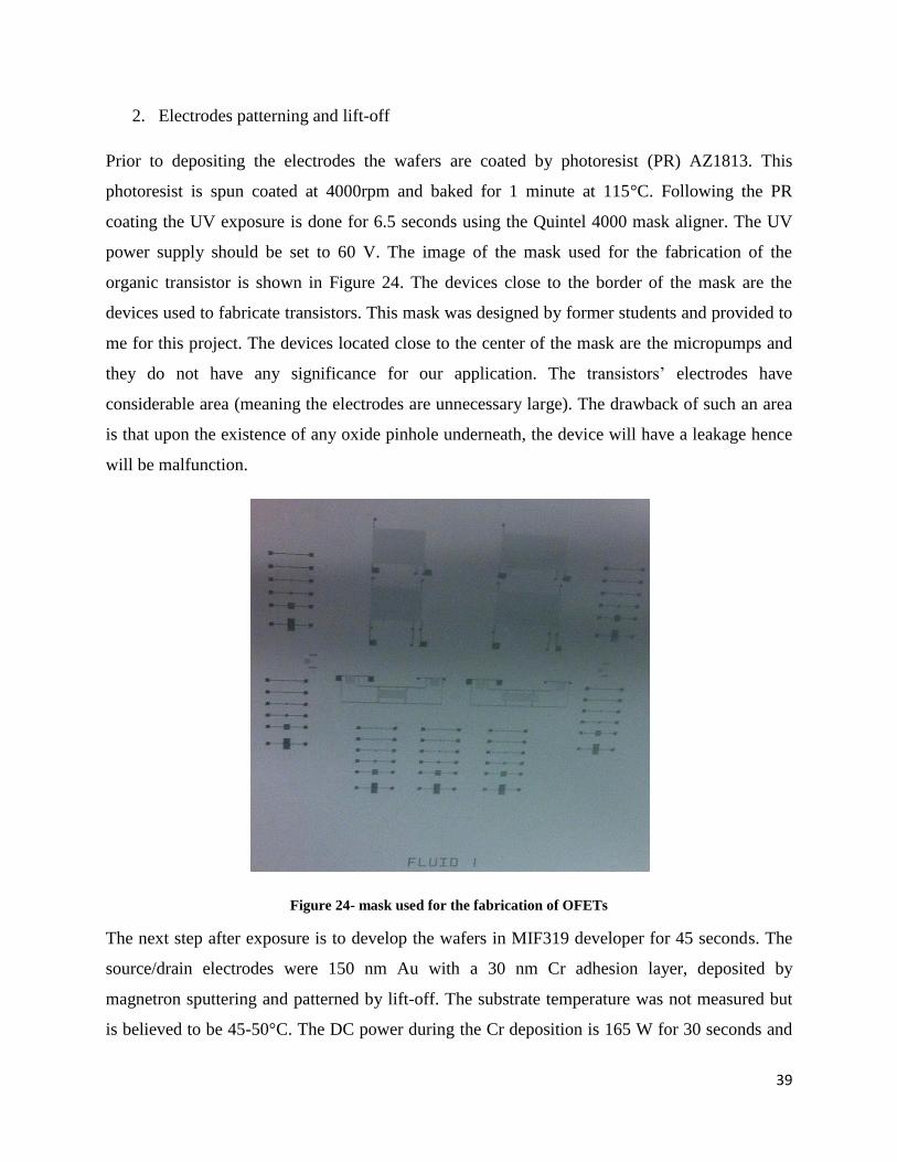
Page 1
Fabrication and Characterization of Pentacene Devices
By: Erfan Kheirkhahi
Supervisor: Prof. Nick McGruer
A THESIS SUBMITTED
IN PARTIAL FULFILLMENT OF THE
REQUIREMENTS FOR THE DEGREE OF
Master of Science
Boston, Massachusetts
November 2011
Page 2
1
Abstract
Organic devices have shown great promise during the past decade. These devices have
several advantages including light weight, flexibility, ease of manufacturability and low cost.
These pros make the organic devices good candidates to replace the current semiconductor
technology in the areas of thin film transistors, photovoltaics and light-emitting diode
fabrication. Pentacene as a conjugated compound1 shows high performance (including high
carrier mobility) among many organic compounds. In contrast to the high electrical performance,
these materials suffer from photo-oxidation, a phenomenon in which the devices degrade over
time.
In this thesis five novel derivatives of pentacene are introduced and electrically
characterized. These compounds were synthesized at the University of New Hampshire2 in Dr.
Glen Miller‟s research group. Later the compounds were given to us for the electrical
characterization. All these materials are photo-oxidation resistant. The photo-oxidation resistance
of these compounds varies as a function of the substituent. As reported by Dr. Miller et al. the
type and the position of the substituent also affect the HOMO-LUMO energies.
The electrical behavior of the transistors made out of three of the derivatives is similar to that of
conventional transistors. The differences between their electrical behavior and that of the
conventional transistors are also discussed. The electrical characteristics of the other two
compounds are suppressed by contact effects. This type of electrical behavior in organic
semiconductor is not thoroughly investigated in the literature. In this thesis possible carrier
injection methods that result in this type of electrical characteristic are discussed. The last part
of this thesis compares the electrical performance (including carrier mobility, threshold voltage
and ON/OFF ratio) of these compounds to some other derivatives of pentacene reported in the
literature.
1 In organic chemistry there is a class of materials that have alternating double bonds and single bonds. This alternation between
bonds is due to the delocalization of the Π-electrons and results in the stability of the compound. These materials are called
conjugated compounds. In conjugated materials there is a single bond between the double bonds therefore the alternation of the
bonds is possible.(i.e. R-C=C-C=C-R ; R:alkyl group)
Other possible configurations in the materials having double bonds are when the double bonds are next to each other (without any
single bond between them) or there are two/more single bonds separating them. Both of these types suffer from instability. The
significance of the conjugated compounds is that the electrical conductivity of them can be controlled through the oxidation and
reduction reactions hence electronic devices can be made out of them. 2 Department of Physics and Materials Science and Department of Chemistry and Materials Science
Page 3
2
Table of Contents
Chapter 1 – Introduction and Background _________________________________________ 4
1.1 Current market for organic devices _______________________________________________ 6
1.2 Electronic structure of organic semiconductors ______________________________________ 8
1.3 Two-terminal organic devices ____________________________________________________ 9
1.3.1) Device operation of Organic LEDs (OLEDs) _______________________________________________ 9
1.3.2) Device operation of Organic Photovoltaic (solar cells) ______________________________________ 10
1.4 Device operation of three terminal devices _________________________________________ 11
1.5 Mechanisms of charge transport and injection in organic semiconductors ______________ 24
1.6 Contact effect in organic field effect transistors _____________________________________ 28
1.7 Contact resistance extraction and measurement methods ____________________________ 30
1.7.1) Transfer Line Method ________________________________________________________________ 30
1.7.2) Four Probe Measurements _____________________________________________________________ 31
1.7.3) Kelvin Probe Force Microscopy ________________________________________________________ 32
1.8 Top contact vs. bottom contact FETs _____________________________________________ 33
1.9 Effect of deposition techniques on the performance _________________________________ 34
1.10 Effect of solvent on the performance _____________________________________________ 35
Chapter 2 – Fabrication and Characterization of OFETs ____________________________ 37
2.1 Device Fabrication Procedure ___________________________________________________ 37
2.2 Thin-film properties and thickness measurements __________________________________ 42
2.3 I-V measurements _____________________________________________________________ 45
2.3.1) Parameter extraction from experiments __________________________________________________ 45
2.3.2) Experimental I-V measurements ________________________________________________________ 47
2.3.2.1) 2,3,9,10-Tetrachloro-6,13-bis(phenethylthio) pentacene _________________________________ 47
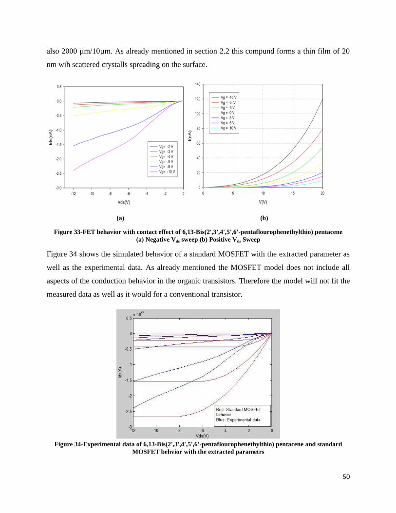
2.3.2.2) 6,13-Bis(2',3',4',5',6'-pentaflourophenethylthio) pentacene _______________________________ 49
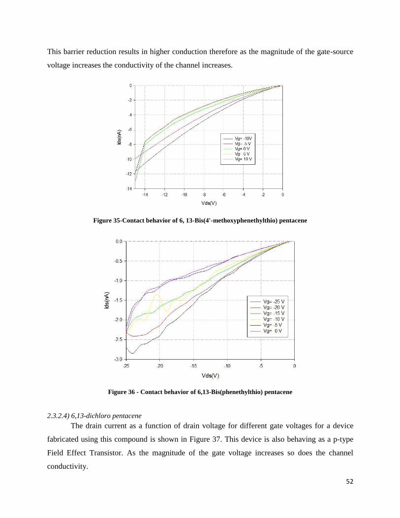
2.3.2.3) 6,13-Bis (4'-methoxyphenethylthio) pentacene & 6,13-Bis(phenethylthio) pentacene __________ 51
2.3.2.4) 6,13-dichloro pentacene ___________________________________________________________ 52
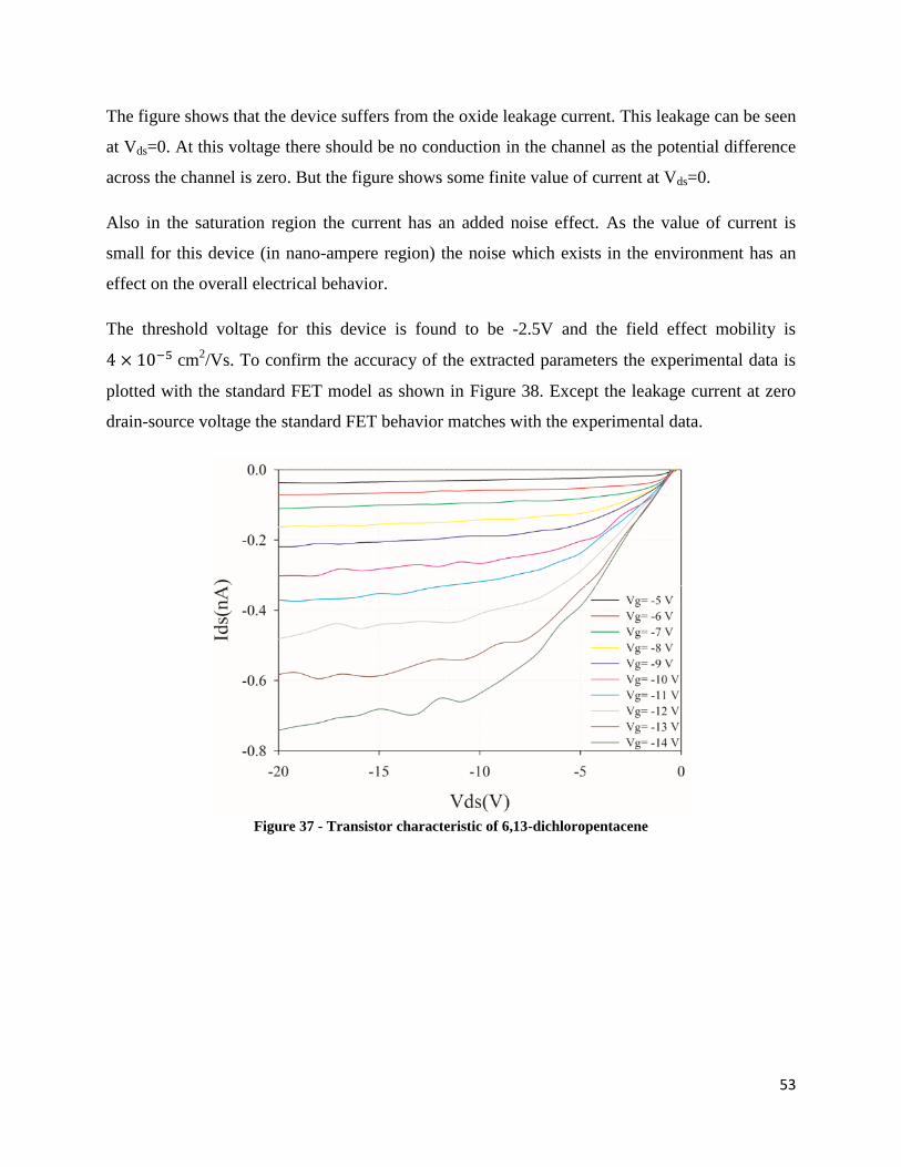
2.4 More discussion about the experimental data ______________________________________ 55
2.5 Comparison of results __________________________________________________________ 55
3. Conclusion and future work _________________________________________________ 56
4. References _______________________________________________________________ 58
Page 4
3
Table of Figures
Figure 1 - Future market of organic devices [17] ..................................................................................................................................................... 7
Figure 2- Few examples of conjugated materials [18] .............................................................................................................................................. 8
Figure 3- Schematic cross section of an OLED [24] ............................................................................................................................................... 10
Figure 4- Schematic of typical p-channel and n-channel field effect transistors [35] ............................................................................................. 13
Figure 5-Current leakages in the on/off state [39] .................................................................................................................................................. 15
Figure 6-N-channel transistor in inversion mode [40] ............................................................................................................................................ 16
Figure 7- IV characteristic of a transistor [41] ....................................................................................................................................................... 17
Figure 8- Possible configurations of organic transistors (a) Bottom gate, top electrodes configuration (b) Bottom gate, bottom electrodes
configuration (c) top gate, bottom electrodes configuration (d) top gate, top electrodes configuration [46] ......................................................... 20
Figure 9 – Bottom gate FET structure with top electrodes [48] .............................................................................................................................. 22
Figure 10- Top electrodes versus bottom electrodes ............................................................................................................................................... 23
Figure 11- Current density vs. voltage for a trap free semiconductor, solid line is the case of the bulk-limited current conduction and the dashed-
line is the contact-limited current conduction [54] ................................................................................................................................................. 24
Figure 12- I-V characteristic of a Schottky barrier [55] ......................................................................................................................................... 26
Figure 13- I-V Energy band diagram of a Schottky diode [55] ............................................................................................................................... 26
Figure 14- I-V characteristic of an ideal and non ideal Schottky diode [54] .......................................................................................................... 28
Figure 15-Schematic of OFET showing equivalent resistances [57] ....................................................................................................................... 28
Figure 16- Pentacene-Au Energy band diagram [57] ............................................................................................................................................. 29
Figure 17-Transfer Line Method- the contact resistance is the channel resistance extrapolated to zero channel length [57] ................................ 30
Figure 18-(a) OFET with two voltage sensing probe (b) ideal channel potential profile(dashed line)/extrapolated potential profile(solid line) [57]
................................................................................................................................................................................................................................ 31
Figure 19- (a) schematic of KFM techniques (b) the measured surface potential profile using KFM [57] ............................................................. 32
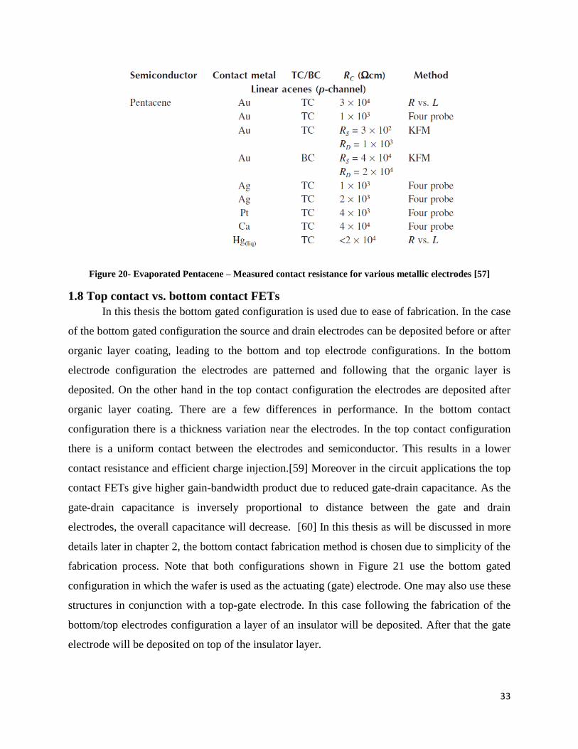
Figure 20- Evaporated Pentacene – Measured contact resistance for various metallic electrodes [57] ................................................................. 33
Figure 21- Top vs. bottom electrode FETs .............................................................................................................................................................. 34
Figure 22- AFM images of pentacene layer spin coated from different solvent. (Measured range is 40 μm × 40 μm). (a) Chlorobenzene. (b)
Chloroform. (c) Toluene (d) p-xylene ...................................................................................................................................................................... 35
Figure 23- Schematic cross section ......................................................................................................................................................................... 37
Figure 24- mask used for the fabrication of OFETs ................................................................................................................................................ 39
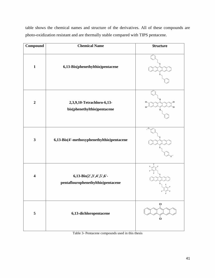
Figure 25- SEM image of the device with channel dimension of W=2000µm, L=10 µm. The large light rectangles are the electrodes (with
electrical connections to the right and left), and the irregular material is the deposited “2,3,9,10-Tetrachloro-6,13-bis(phenethylthio)pentacene”
after spin coating and baking .................................................................................................................................................................................. 42
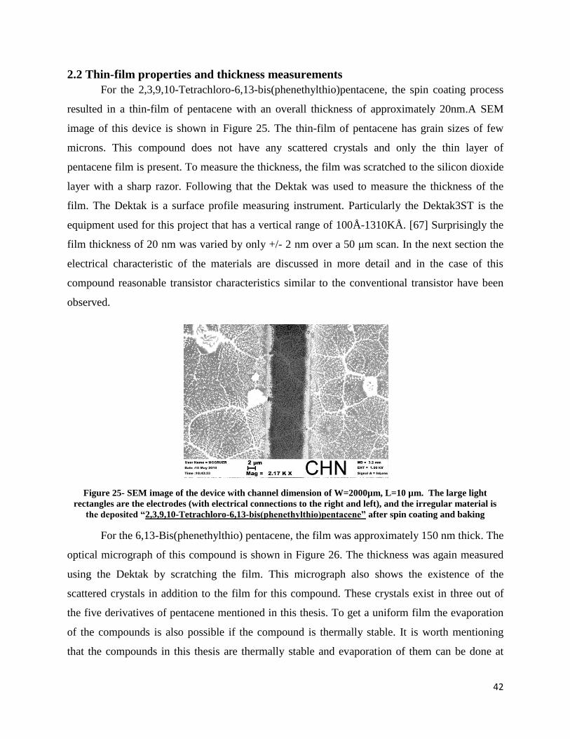
Figure 26- 6,13-Bis(phenethylthio) pentacene –optical micrograph ....................................................................................................................... 43
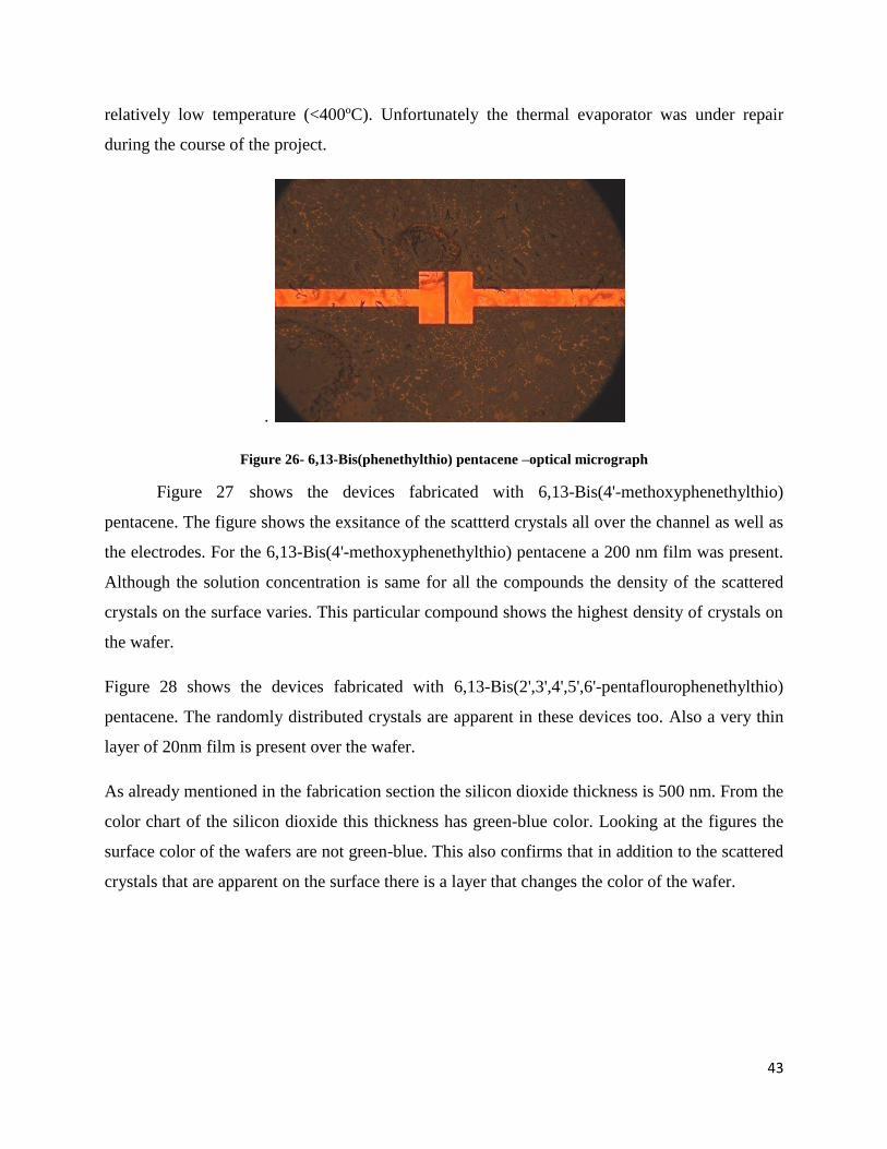
Figure 27- 6,13-Bis(4'-methoxyphenethylthio)pentacene ........................................................................................................................................ 44
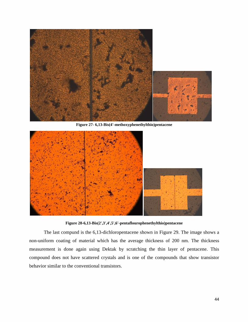
Figure 28-6,13-Bis(2',3',4',5',6'-pentaflourophenethylthio)pentacene ..................................................................................................................... 44
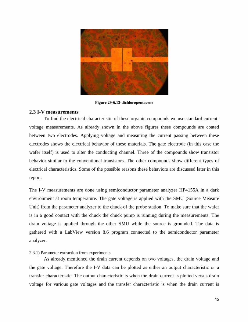
Figure 29-6,13-dichloropentacene .......................................................................................................................................................................... 45
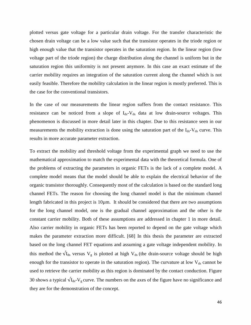
Figure 30- Mobility extraction using extrapolation [69] ......................................................................................................................................... 47
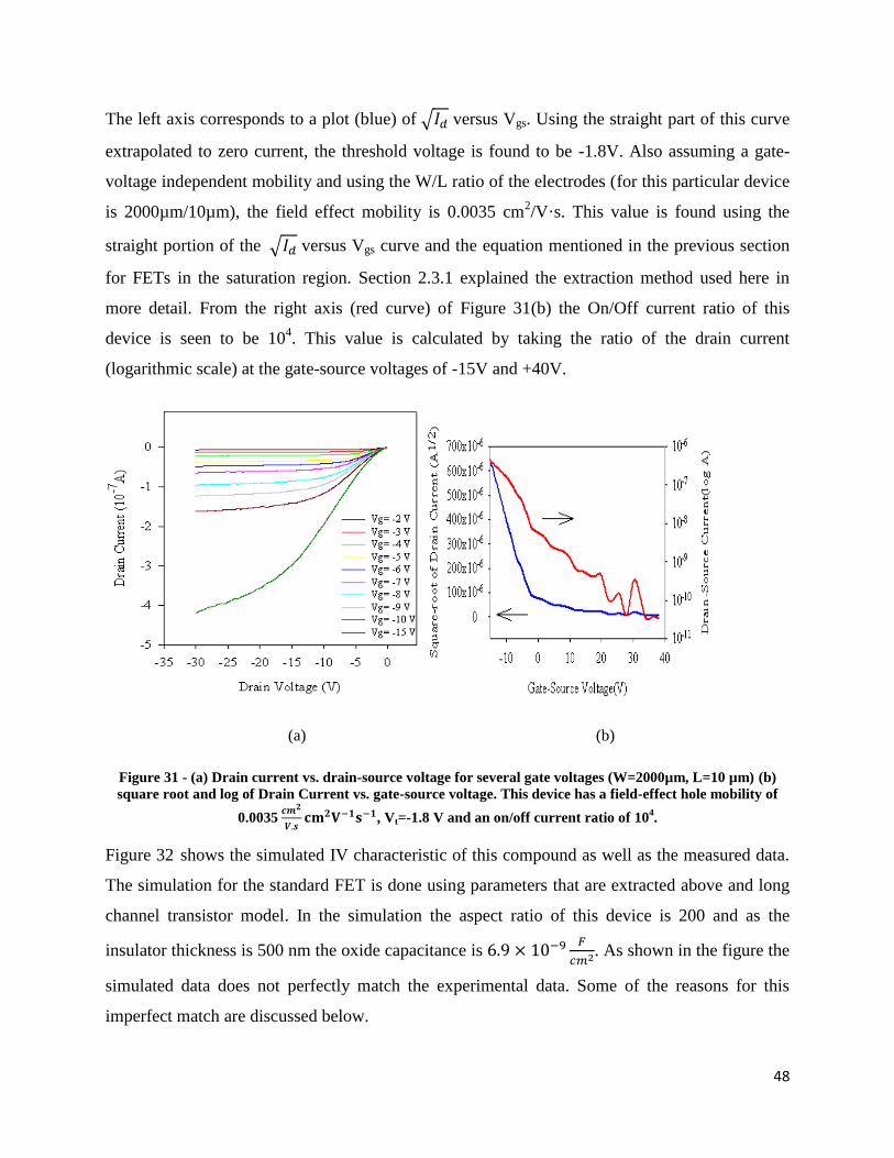
Figure 31 - (a) Drain current vs. drain-source voltage for several gate voltages (W=2000µm, L=10 µm) (b) square root and log of Drain
Current vs. gate-source voltage. This device has a field-effect hole mobility of 0.0035
, Vt=-1.8 V and an on/off current ratio of 104. ............. 48
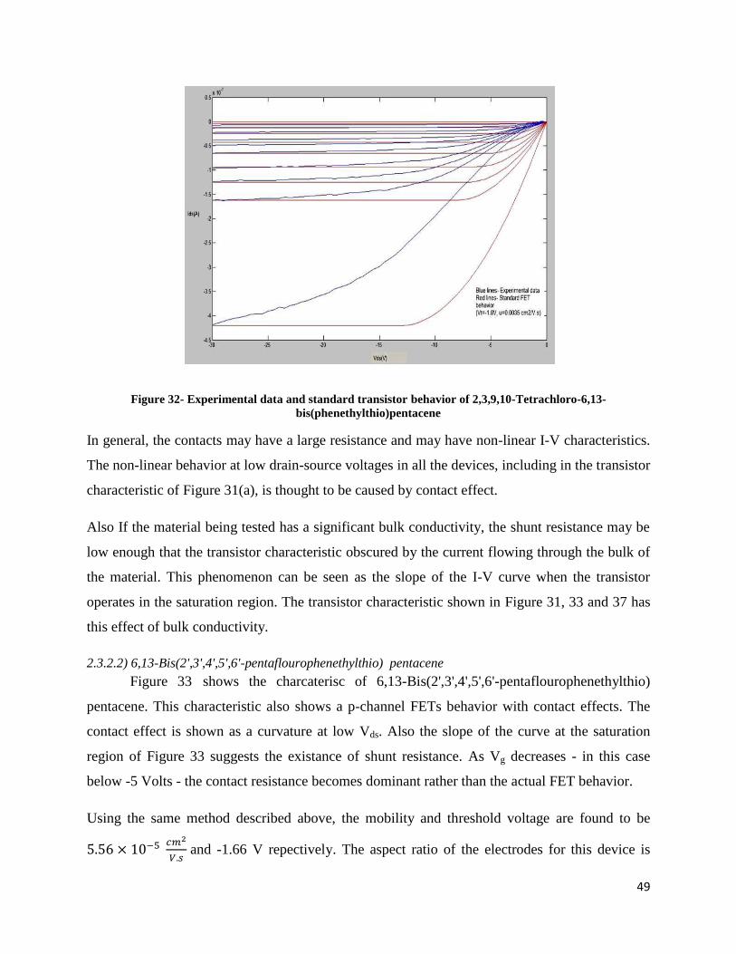
Figure 32- Experimental data and standard transistor behavior of 2,3,9,10-Tetrachloro-6,13-bis(phenethylthio)pentacene ................................. 49
Figure 33-FET behavior with contact effect of 6,13-Bis(2',3',4',5',6'-pentaflourophenethylthio) pentacene (a) Negative Vds sweep (b) Positive
Vds Sweep ................................................................................................................................................................................................................. 50
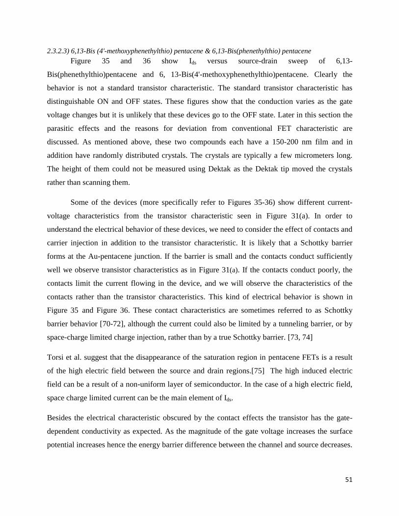
Figure 34-Experimental data of 6,13-Bis(2',3',4',5',6'-pentaflourophenethylthio) pentacene and standard MOSFET behvior with the extracted
parametrs ................................................................................................................................................................................................................ 50
Figure 35-Contact behavior of 6, 13-Bis(4'-methoxyphenethylthio) pentacene ....................................................................................................... 52
Figure 36 - Contact behavior of 6,13-Bis(phenethylthio) pentacene ....................................................................................................................... 52
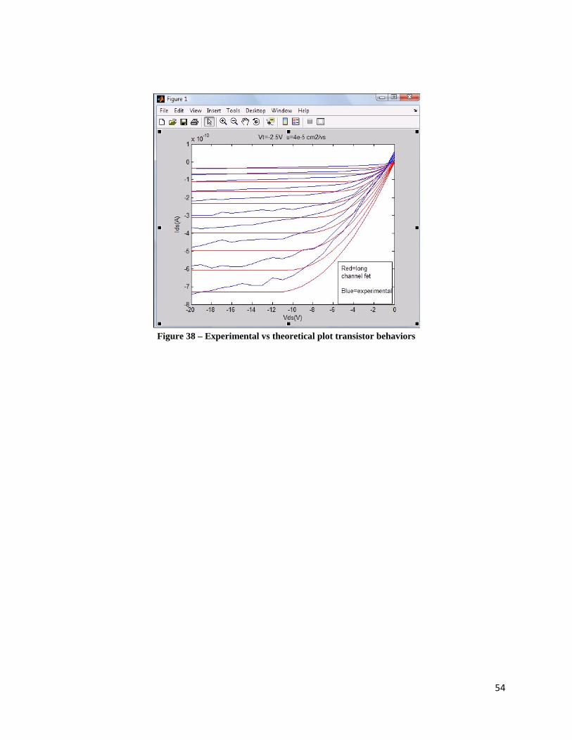
Figure 37 - Transistor characteristic of 6,13-dichloropentacene ............................................................................................................................ 53
Figure 38 – Experimental vs theoretical plot transistor behaviors .......................................................................................................................... 54
Page 5
4
Chapter 1 – Introduction and Background
Organic semiconducting materials have been synthesized and used in various applications
for over five decades.[1] These materials have important properties such as flexibility, light
weight and relatively easy manufacturability. These advantages are promising for future
generations of organic devices especially in light emitting diodes (LED) and photovoltaic
applications. Having flexible displays or wearable solar panels have been made possible using
this branch of device manufacturing. On the other hand these materials often suffer from poor
performance and lifetime. From the electronic perspective, the performance of the organic
devices is limited in speed (carrier mobility), operating voltage and power consumption.
Pentacene molecules are known to have high carrier mobility in compared with many
other organic compounds. The reported mobility for pentacene deposited using thermal
evaporation in 1991 was 0.002 cm2/Vs by Horwitz et al. Later during 1996-1997 the mobility of
the transistors fabricated using pentacene was dramatically increased and reached the value of
1.5 cm2/Vs. This three order of magnitude increment is attributed to the choice of the dielectric
material and surface treatment of the gate dielectric. It has been shown that self assembled
monolayer (SAM) of HMDS is a proper choice prior the deposition of the pentacene thin-film.
The value of the mobility of the transistors fabricated with pentacene molecules has been
increasing to 3.0, 3.3, 5.5, 6.3 and finally 8.85 cm2/Vs. The last value (8.85 cm
2/Vs) reported on
January 2011 is a transistor fabricated using Barium Titanate oxide gate insulator. [2, 3]
Matching the surface energy of the dielectric and the pentacene layer is known to enhance the
electrical performance especially the carrier mobility of the pentacene transistors. The matching
of the surface energies is an important factor in the fabrication of the organic transistors and will
be addressed later in this thesis. As already mentioned above, the pentacene devices show high
carrier mobility in compared with other organic devices.
There are many organic compounds available but here I limit the comparison to three
compounds widely used in organic photovoltaic and light emitting diodes. Poly (3-
Hexylthiophene) abbreviated as P3HT has a carrier mobility range of 0.01-0.1cm2/Vs. This
compound has been used in organic photovoltaic and OTFT. Poly (p-phenylene vinylene) (PPV)
and polyfluorene (F8T2) are two other widely used compounds especially in OLEDs. The carrier
mobility ranges for these two compounds are 0.00001-0.0001 and 0.001-0.01 cm2/Vs
Page 6
5
respectively. [4] The comparison of the carrier mobility for various compounds is beyond the
scope of this thesis.
To get more idea about the carrier mobility it is worth comparing the carrier mobility of the
silicon technology with the pentacene devices. The range of the carrier mobility for the
amorphous silicon is 0.4-4 cm2/Vs and for the polycrystalline silicon can reach to 100 cm
2/Vs.
[5, 6] Also the electron and hole mobility of the single crystalline silicon are 1450 and 500
cm2/Vs respectively.[7] Therefore currently the carrier mobility of the pentacene devices is
comparable with the amorphous silicon devices.
Earlier it is mentioned that the electrical performance of the pentacene transistors
(generally organic transistors) is limited in carrier mobility, operating voltage and power
consumption. The carrier mobility of the pentacene transistors has been discussed above. Other
performance criteria are the operating voltage and power consumption. A major factor
influencing these criteria is the threshold voltage of the transistors. Generally lower threshold
voltage is desirable as a lower turn-on voltage will be needed for the device to operate. So far the
threshold voltage for the pentacene transistors is not thoroughly investigated in the literature.
Later in this thesis some of the factors that change this voltage are discussed. Apparently this
voltage in pentacene transistors same as the conventional transistors depends on the gate
insulator thickness and its dielectric constant as well as the work-function of the gate electrode.
Also the thickness of the pentacene layer shifts the value of the threshold voltage. To be able to
use the pentacene devices for low power and portable devices the value of the threshold voltage
should be low and controllable. This means that depending on the designed circuit the device
engineer should be able to adjust the value of this voltage.
The aim of this research is to electrically characterize the three-terminal devices
fabricated using five derivatives of pentacene. The pentacene derivatives act as the
semiconducting channel in the devices. This thesis starts with the introduction of various organic
devices and their principle of operation. This discussion includes organic photovoltaic, light
emitting diodes and organic transistors. In addition to the principle of operation the mechanism
of charge injection in organic transistors and the effect of contacts are discussed. Later in the
chapter various fabrication methods and their effect on the electrical performance are discussed.
The second chapter of this thesis focused on the fabrication and characterization of five novel
Page 7
6
derivatives of pentacene. This chapter includes the discussion of the properties of the materials,
the electrical behavior of them and the comparison of the results with the current literature.
1.1 Current market for organic devices
Currently the majority of market for the organic devices is in the OLED devices. Some
unique properties of organic LEDs such as flexibility, large viewing angle, brightness and large
color range make it desirable to replace the inorganic technology.[8] In fact, in 2002 Philips
introduced the Sensotec Philishave razor as the first product in the market featuring an OLED
display.[9] Later on Samsung and LG introduced OLED TVs and flat panel displays. Canon and
Kodak also changed the technology of all the products such as cameras, camcorders and InkJet
printers to OLEDs.[10] One of the technical challenges in OLEDs is the life time of the devices.
The life time of the OLEDs changes as the color changes. So far blue color has the most limited
life time among other colors of OLEDs. Kodak and UDC have both made strides in developing
long‐lived RGB displays with small molecules. UDC has been boosting the life time of the red
OLED from 25 Khrs (at 200 nits3) in 2005 to 300 Khrs (at 500 nits) in 2006. [11] As far as May
2011, the company rated the life time of their red OLED to be 900 Khrs. Meanwhile the
company rated their yellow-green OLED lifetime to be 1.4 million hours and their blue OLED to
be 20 Khrs. [12]
The organic transistors have potential market in the areas of radio frequency
identification tags (RFIDs) and e-book/e-paper. According to NanoMarkets, OTFTs are already
proving themselves in the e-paper backplanes market and this market will reach $3.3 billion by
2015. [13] The OFET devices used as RFID tags are still in research communities. To be used in
RFID tags the organic TFTs should have high carrier mobility to allow the device to operate in
the high frequencies (MHz/GHz). The market and total investments on the organic RFIDs is
projected to be worth $4 billion by 2018. [14]
Another application of the organic devices is in printed and organic sensors. Besides the
low price of manufacturing the flexible organic sensors can be manufactured on many different
substrates in many different shapes for medical, architecture, protective clothing, smart label and
packaging, robotics, aerospace and automotive applications. Biosensors as a major part of the
sensor market can be used to diagnose muscular and bone diseases. By 2015 the printed organic
3 A nit (in SI unit) is candela per square meter.(candela is a Luminous Intensity)
Page 8
7
medical diagnostic and therapeutic sensor market (microarrays and biochips excluded) is
predicted to reach $414 million.[15]
Other application of organic devices is in photovoltaics. The lower cost of OPVs
compared to silicon cells and easy manufacturing are the major advantages of these devices.
Also continuous printing of them even on the flexible substrate is one of the many attractive
features that organic PVs have. Currently organic solar cells suffer from insufficient power
conversion efficiency and lifetime. To commercialize them the industry needs a power
conversion efficiency of ~10% with a few years life time.[16]
The market forecast including various organic devices predicted by 2027 is shown in
Figure 1. Currently the research areas are more focused on photovoltaic and memory application
in which the companies are interested to commercialize soon.[17]
Figure 1 - Future market of organic devices [17]
Organic materials including pentacene molecules have relatively low mobility and switching
speed. As mentioned above most of the applications of organic devices need an improvement in
the stability of the compounds as well as other performance criteria such as the mobility and
ON/OFF ratio. It is worth in here to mention that the aim of this thesis is to characterize the
derivatives of pentacene and compare their electrical performance with some other reported
compounds. In addition, from the device theory stand point this thesis discusses various impacts
of the device fabrication on the electrical performance.
Page 9
8
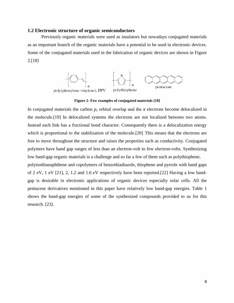
1.2 Electronic structure of organic semiconductors
Previously organic materials were used as insulators but nowadays conjugated materials
as an important branch of the organic materials have a potential to be used in electronic devices.
Some of the conjugated materials used in the fabrication of organic devices are shown in Figure
2.[18]
Figure 2- Few examples of conjugated materials [18]
In conjugated materials the carbon pz orbital overlap and the π electrons become delocalized in
the molecule.[19] In delocalized systems the electrons are not localized between two atoms.
Instead each link has a fractional bond character. Consequently there is a delocalization energy
which is proportional to the stabilization of the molecule.[20] This means that the electrons are
free to move throughout the structure and raises the properties such as conductivity. Conjugated
polymers have band gap ranges of less than an electron-volt to few electron-volts. Synthesizing
low band-gap organic materials is a challenge and so far a few of them such as polythiophene,
polyisothianaphthene and copolymers of benzothiadiazole, thiophene and pyrrole with band gaps
of 2 eV, 1 eV [21], 2, 1.2 and 1.6 eV respectively have been reported.[22] Having a low band-
gap is desirable in electronic applications of organic devices especially solar cells. All the
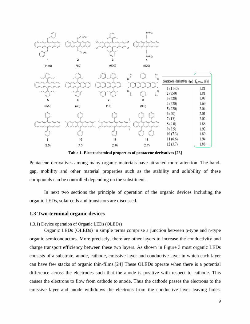
pentacene derivatives mentioned in this paper have relatively low band-gap energies. Table 1
shows the band-gap energies of some of the synthesized compounds provided to us for this
research. [23].
Page 10
9
Table 1- Electrochemical properties of pentacene derivatives [23]
Pentacene derivatives among many organic materials have attracted more attention. The band-
gap, mobility and other material properties such as the stability and solubility of these
compounds can be controlled depending on the substituent.
In next two sections the principle of operation of the organic devices including the
organic LEDs, solar cells and transistors are discussed.
1.3 Two-terminal organic devices
1.3.1) Device operation of Organic LEDs (OLEDs)
Organic LEDs (OLEDs) in simple terms comprise a junction between p-type and n-type
organic semiconductors. More precisely, there are other layers to increase the conductivity and
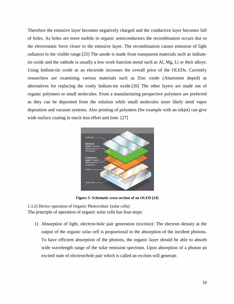
charge transport efficiency between these two layers. As shown in Figure 3 most organic LEDs
consists of a substrate, anode, cathode, emissive layer and conductive layer in which each layer
can have few stacks of organic thin-films.[24] These OLEDs operate when there is a potential
difference across the electrodes such that the anode is positive with respect to cathode. This
causes the electrons to flow from cathode to anode. Thus the cathode passes the electrons to the
emissive layer and anode withdraws the electrons from the conductive layer leaving holes.
Page 11
10
Therefore the emissive layer becomes negatively charged and the conductive layer becomes full
of holes. As holes are more mobile in organic semiconductors the recombination occurs due to
the electrostatic force closer to the emissive layer. The recombination causes emission of light
radiation in the visible range.[25] The anode is made from transparent materials such as indium-
tin oxide and the cathode is usually a low work function metal such as Al, Mg, Li or their alloys.
Using Indium-tin oxide as an electrode increases the overall price of the OLEDs. Currently
researchers are examining various materials such as Zinc oxide (Aluminum doped) as
alternatives for replacing the costly Indium-tin oxide.[26] The other layers are made out of
organic polymers or small molecules. From a manufacturing perspective polymers are preferred
as they can be deposited from the solution while small molecules more likely need vapor
deposition and vacuum systems. Also printing of polymers (for example with an inkjet) can give
wide surface coating in much less effort and time. [27]
Figure 3- Schematic cross section of an OLED [24]
1.3.2) Device operation of Organic Photovoltaic (solar cells)
The principle of operation of organic solar cells has four steps:
1) Absorption of light, electron-hole pair generation (exciton): The electron density at the
output of the organic solar cell is proportional to the absorption of the incident photons.
To have efficient absorption of the photons, the organic layer should be able to absorb
wide wavelength range of the solar emission spectrum. Upon absorption of a photon an
excited state of electron/hole pair which is called an exciton will generate.
Page 12
11
2) Exciton diffusion: The exciton needs to travel a distance to reach the dissociation site.
Exciton diffusion lengths in the organic compounds are usually around 10 nm although
some compounds such as the perylenes has 100nm diffusion length.
3) Charge separation at donor/acceptor interface: Charge separation is a phenomenon in
which the negative and positive charges dissociate from an exciton. This separation
occurs because of the energy difference between the layers of the cell.
4) The holes will go to the anode and the electrons will go to the cathode.[28]
The field of organic photovoltaics dates back to 1959 when Kallman and Pope discovered
that anthracene showed a photo-voltage of 0.2 V. Although the efficiency of this prototype was
extremely low, it opened the new field of organic solar cells [29]. Later, Tang suggested that
stacking electron donor (D) and electron acceptor (A) layers, so called bilayer heterojunctions,
increases the transport efficiency of PVs.[30] Using the bilayer hetereojunction has some
drawbacks. Since the diffusion length is typically few nanometers (5-7 nm in C60) not all the
excitons are able to reach donor/acceptor interface.[31] In 1995 Yu et al. showed that by
intimately mixing both components the interfacial area is significantly increased and the distance
that excitons travel is greatly reduced.[32] This structure is the so called bulk heterojunction
(BHJ) and since its introduction has been used extensively for solar cell fabrication. As
mentioned previously one of the drawbacks of current solar cells is the lack of stability and
lifetime. So far researches on increasing the stability of the bulk heterojunction structure have
resulted in one year stability with encapsulation. [33]
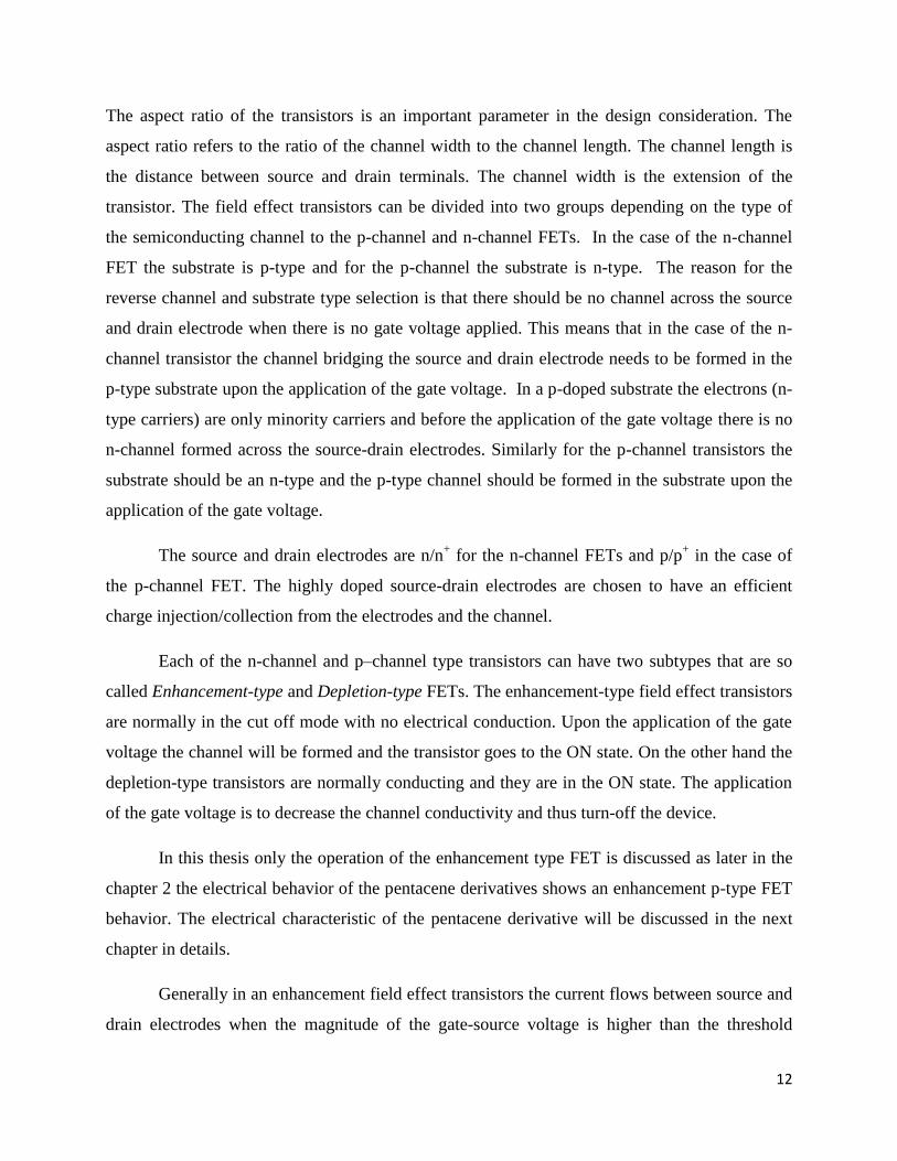
1.4 Device operation of three terminal devices
A typical structure of a field effect transistor is shown in Figure 4 [34]. This structure
consists of a substrate, doped regions of semiconductors called source/drain, the source/drain
metallic contacts, insulator layer (usually silicon dioxide) and the gate electrode. The gate
electrode can be either metallic or silicon/poly-silicon gate. Later on the schematic of the
organic field effect transistors is mentioned in this section. There are a few differences of the
organic transistor architecture with the conventional transistors. Since the electrical conduction
is controlled using the gate, source, drain and substrate terminals, the field effect transistor is a
four terminal device. Sometimes the field effect transistor is said to have only three terminals.
This refers to a condition that the source and substrate terminals are connected together.
Page 13
12
The aspect ratio of the transistors is an important parameter in the design consideration. The
aspect ratio refers to the ratio of the channel width to the channel length. The channel length is
the distance between source and drain terminals. The channel width is the extension of the
transistor. The field effect transistors can be divided into two groups depending on the type of
the semiconducting channel to the p-channel and n-channel FETs. In the case of the n-channel
FET the substrate is p-type and for the p-channel the substrate is n-type. The reason for the
reverse channel and substrate type selection is that there should be no channel across the source
and drain electrode when there is no gate voltage applied. This means that in the case of the n-
channel transistor the channel bridging the source and drain electrode needs to be formed in the
p-type substrate upon the application of the gate voltage. In a p-doped substrate the electrons (n-
type carriers) are only minority carriers and before the application of the gate voltage there is no
n-channel formed across the source-drain electrodes. Similarly for the p-channel transistors the
substrate should be an n-type and the p-type channel should be formed in the substrate upon the
application of the gate voltage.
The source and drain electrodes are n/n+ for the n-channel FETs and p/p
+ in the case of
the p-channel FET. The highly doped source-drain electrodes are chosen to have an efficient
charge injection/collection from the electrodes and the channel.
Each of the n-channel and p–channel type transistors can have two subtypes that are so
called Enhancement-type and Depletion-type FETs. The enhancement-type field effect transistors
are normally in the cut off mode with no electrical conduction. Upon the application of the gate
voltage the channel will be formed and the transistor goes to the ON state. On the other hand the
depletion-type transistors are normally conducting and they are in the ON state. The application
of the gate voltage is to decrease the channel conductivity and thus turn-off the device.
In this thesis only the operation of the enhancement type FET is discussed as later in the
chapter 2 the electrical behavior of the pentacene derivatives shows an enhancement p-type FET
behavior. The electrical characteristic of the pentacene derivative will be discussed in the next
chapter in details.
Generally in an enhancement field effect transistors the current flows between source and
drain electrodes when the magnitude of the gate-source voltage is higher than the threshold
Page 14
13
voltage (|Vgs|>|Vt|). In the case of the enhancement n-channel field effect transistors
(enhancement NFET) the gate-source voltage and the threshold voltage are both positive. To turn
on an enhancement n-channel field effect transistors the gate-source voltage should be higher
than the threshold voltage (Vgs>Vt). In contrast in the case of the p-channel field effect transistors
(PFET) the gate-source and threshold voltages are negative. For the P-channel FET to turn on,
the gate-source voltage should be smaller than the threshold voltage (Vgs<Vt). [35]
Figure 4- Schematic of typical p-channel and n-channel field effect transistors [35]
Ideally, when the transistor is in the off state, there is no current flowing through the
channel and therefore the power dissipation of the device in this state is zero. But in the real case
the transistors suffer from several leakage paths. The leakage currents and their effect on the
performance criteria such as power dissipation are important therefore it is worth mentioning the
possible leakage paths in here. One of the leakage currents that may be seen in the transistors is
due to the pinholes in the insulator. This leakage current increases as the magnitude of the gate
voltage increases. The reason behind this type of leakage is an imperfect cleaning and insulator
deposition and/or growth procedure. It is known that for silicon, wet oxidation method (oxidation
using water molecules) may result in more pinholes than dry oxidation method (oxidation using
oxygen molecules). Another possible oxide leakage path is tunneling of the charged particles.
This tunneling effect increases as the oxide thickness decreases. Especially this type of leakage is
an important phenomenon in the nano-scale devices in which the oxide thickness scales down to
the nanometer regime. To overcome this oxide leakage the researchers have introduced high-K
dielectrics. These dielectrics should have large K (dielectric constant) and be able to have good
Page 15
14
interface contact to the substrate and gate electrode. Typical high-K dielectrics are HfO2 (K~25),
ZrO2 (K~25), TiO2 (K~80). [36]
Another important leakage current is the subthreshold leakage. Subthreshold leakage is a
current between source and drain electrodes when the magnitude of the gate-source voltage is
less than the magnitude of the threshold voltage (meaning that the transistor is in the off state).
As the magnitude of the threshold voltage shrinks the effect of the subthreshold current will be
more apparent.
Another possible current path is between the source and drain electrodes. In general as
the size of the channel decreases (here the size of the channel refers to the channel length “L”)
other effects that are called short channel effects may occur. The reduction in the channel length
results in high induced electric field. This high electric field can damage the interface of channel
with the electrodes. The damage results in degradation of mobility and shift in the threshold
voltage over a time period.[37, 38] Moreover the high electric field in the channel can result in
the Hot Carrier Injection (HCI) phenomena. The HCI occurs when the carriers (either electrons
or holes) have sufficient energy to overcome the silicon dioxide barrier (in general the insulator
layer) and penetrate to that layer. The term “hot” refers to the effective temperature used to
model carrier density and not to the overall temperature of the device.
The short channel effects are the reliability issues as they change the threshold voltage of
the device. Sometimes this shift of the threshold voltage is such that the device never turns off;
therefore in this case the short channel effect is a leakage path.
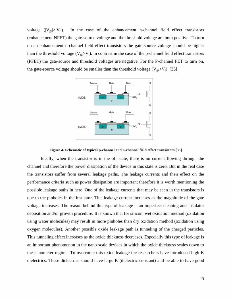
Let‟s consider a nano-scale transistor as shown in Figure 5 in the OFF-state and the ON-
state. In the OFF-state of the transistor the main types of leakage currents are shown. The GIDL
(Gate Induced Drain Leakage) leakage is a current between drain and substrate due to high
electric field between gate and drain. When the FET is in the standby mode the drain terminal is
connected to the power supply while the gate is grounded. This can induce a high electric field
hence unwanted current conduction. Also as we know there are p-n junctions between
source/drain and substrate. In the case of the reverse bias, this junction will conduct and results
in a leakage current. This leakage current is known as BTBT (Band to Band tunneling) current
shown in Figure 5(a).
Page 16
15
These current leakages increase the power consumption of the transistor even in the OFF
state. The FET should dissipate no power while it is in the OFF state. Figure 5(a) shows that in
the OFF-state the total leakage current is considerable meaning that as the transistor scales down
the OFF state current increases. This is in contrast with the desired properties of a transistor.
Also as the transistor scales down the contact resistances become more effective and they result
in the reduction of the ON current. The contact resistance as its name implies is a resistance at
the interface of the electrodes and channel. In the conventional FET the contact resistance has
negligible effect on the channel resistance but as the device scales down the effect of this
resistance becomes more significant on the overall electrical behavior of the device.[39]
Figure 5-Current leakages in the on/off state [39]
The transistor operation is based on the applied voltages at the electrodes. In other words
the operation is based on the voltage differences across the electrodes. These voltage differences
are known as VGS (VG-VS) and VDS (VD-VS).VGS is an actuating voltage meaning that the
conductivity of the channel can be controlled using this voltage difference.VDS is a sensing
element meaning that the current passing along the drain-source electrodes can be measured
based on the voltage difference across these electrodes. To be more specific let‟s consider an n-
type field effect transistor. As mentioned earlier to have an n-type transistor operation the
channel formed across the source-drain electrodes should be n-type (electron conduction).
Initially if the positive voltage is applied at the gate-source electrodes this voltage repels the
positive charges at the interface of the insulator and semiconducting channel. This will happen at
VGS<VT (VGS and VT are both positive quantities). This results in the depletion of the channel
from the holes (positive charges). If VGS increases (VGS>VT) the channel becomes inverted
meaning that the electrons becomes induced at the interface of the insulator and the
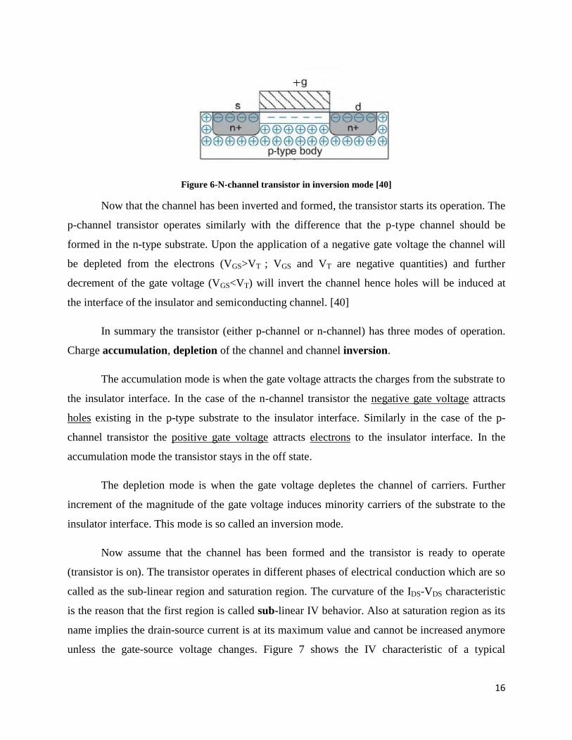
semiconducting channel. A schematic of the inversion mode is in Figure 6.
Page 17
16
Figure 6-N-channel transistor in inversion mode [40]
Now that the channel has been inverted and formed, the transistor starts its operation. The
p-channel transistor operates similarly with the difference that the p-type channel should be
formed in the n-type substrate. Upon the application of a negative gate voltage the channel will
be depleted from the electrons (VGS>VT ; VGS and VT are negative quantities) and further
decrement of the gate voltage (VGS<VT) will invert the channel hence holes will be induced at
the interface of the insulator and semiconducting channel. [40]
In summary the transistor (either p-channel or n-channel) has three modes of operation.
Charge accumulation, depletion of the channel and channel inversion.
The accumulation mode is when the gate voltage attracts the charges from the substrate to
the insulator interface. In the case of the n-channel transistor the negative gate voltage attracts
holes existing in the p-type substrate to the insulator interface. Similarly in the case of the p-
channel transistor the positive gate voltage attracts electrons to the insulator interface. In the
accumulation mode the transistor stays in the off state.
The depletion mode is when the gate voltage depletes the channel of carriers. Further
increment of the magnitude of the gate voltage induces minority carriers of the substrate to the
insulator interface. This mode is so called an inversion mode.
Now assume that the channel has been formed and the transistor is ready to operate
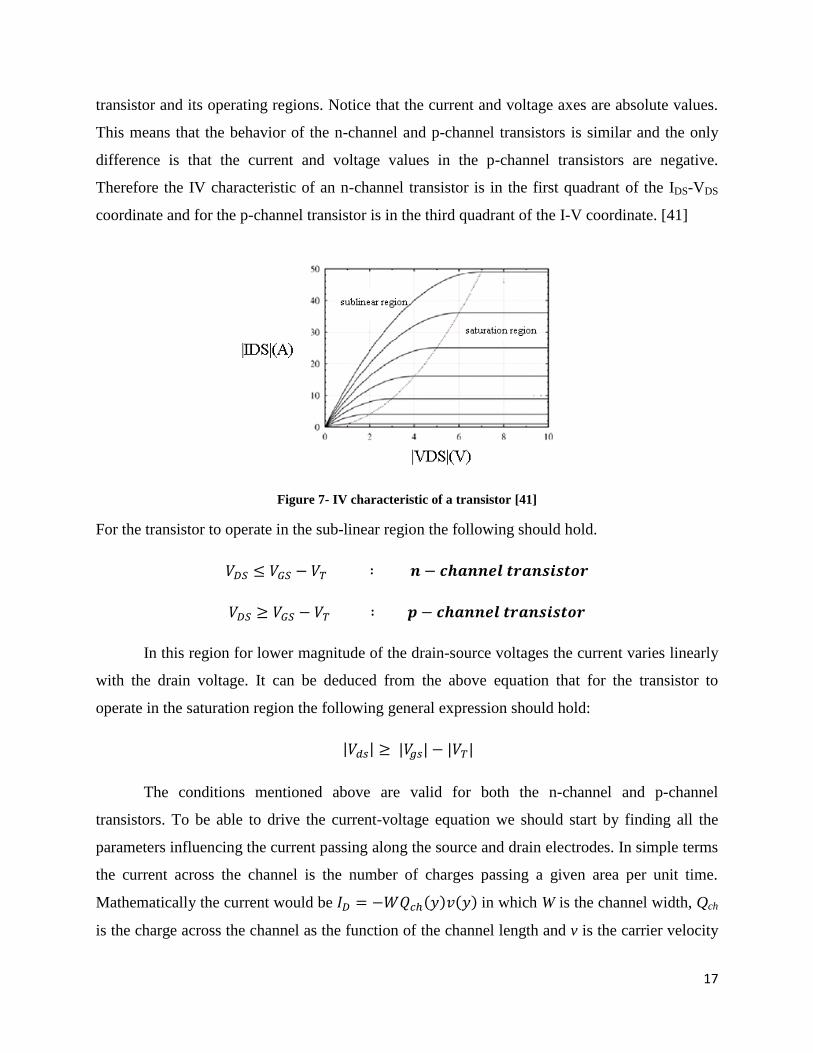
(transistor is on). The transistor operates in different phases of electrical conduction which are so
called as the sub-linear region and saturation region. The curvature of the IDS-VDS characteristic
is the reason that the first region is called sub-linear IV behavior. Also at saturation region as its
name implies the drain-source current is at its maximum value and cannot be increased anymore
unless the gate-source voltage changes. Figure 7 shows the IV characteristic of a typical
Page 18
17
transistor and its operating regions. Notice that the current and voltage axes are absolute values.
This means that the behavior of the n-channel and p-channel transistors is similar and the only
difference is that the current and voltage values in the p-channel transistors are negative.
Therefore the IV characteristic of an n-channel transistor is in the first quadrant of the IDS-VDS
coordinate and for the p-channel transistor is in the third quadrant of the I-V coordinate. [41]
Figure 7- IV characteristic of a transistor [41]
For the transistor to operate in the sub-linear region the following should hold.
In this region for lower magnitude of the drain-source voltages the current varies linearly
with the drain voltage. It can be deduced from the above equation that for the transistor to
operate in the saturation region the following general expression should hold:
The conditions mentioned above are valid for both the n-channel and p-channel
transistors. To be able to drive the current-voltage equation we should start by finding all the
parameters influencing the current passing along the source and drain electrodes. In simple terms
the current across the channel is the number of charges passing a given area per unit time.
Mathematically the current would be in which W is the channel width, Qch
is the charge across the channel as the function of the channel length and v is the carrier velocity
Page 19
18
as the function of the channel length. The “y” in the equation represents the current direction
from the source electrode to the drain electrode. The reason for the negative sign is that in the
case of the p-channel transistor in which the Qch is positive if we apply negative voltage to the
drain electrode and ground the source electrode the direction of the current will be from source to
drain. This means that the drain to source current should have a negative sign implicating the
reverse direction of the current. Similarly in the case of the n-channel transistors in which the Qch
is negative if we apply positive voltage to the drain electrode and ground the source electrode the
direction of the current is from drain to source. Therefore in the case of the n-channel transistor
the negative sign in the equation should exist to have a positive drain-source current. The drain
current equation mentioned above is a general equation for any type of FET.
As the pentacene derivatives show p-channel transistor behavior, rest of the current equation
derivation will be based on the p-channel FET. As already mentioned the current equation for
the transistor is: . In this equation „v’ the carrier velocity is the product of
the carrier mobility µ(y), and the electric field along the channel εL(y). Substituting the equation
for the carrier velocity into the general current equation we find the channel current to be:
To finalize the current equation we should find the equation for the charges along the channel.
As we may already know in a capacitor we have Q=CV in which „C‟ is the capacitance and the
„V‟ is the potential difference across the capacitor. Similarly the charge in the channel is the
product of the voltage difference across the channel and the capacitance. The capacitance is the
insulator capacitance and if the silicon dioxide is used it is denoted as Cox4. The voltage on the
top electrode (gate electrode) is VSG-|VT| and on the lower plate of electrode (channel) is VCH(y).
The later is the voltage between the channel and ground. This voltage varies as the function of
position „y‟ along the channel. Therefore the total voltage difference across the capacitor (COX) is
(VSG-|VT|)-VCH(y). Substituting in the general equation yields:
4 COX=εox/tox ; εox is the permittivity of the silicon dioxide and tox is the silicon dioxide thickness
Page 20
19
The electric field „εL‟ is the voltage difference over a distance
. The voltage across the
channel changes from VSD to zero. Also „y‟ in the equation changes from 0 at the source
electrode to L (channel length) at the drain electrode. Therefore substituting the formula for the
electric field in the above equation and integrating the equation we get the current-voltage
equation for the p-channel field effect transistor as:
This equation is known as the equation for the p-channel transistor in the sub-linear region. To
find the maximum possible value of the current (saturation region) presumably all the VSG-|VT|
voltage dropped along the channel. This means that VSD=VSG-|VT|. Substituting this expression
in the above equation results in the saturation region equation as:
All the mentioned equations assume gate independent field effect mobility and gradual channel
approximation. The carrier field effect mobility decreases as the magnitude of the gate-source
voltage increases. The reason for this decrement is that increasing the magnitude of the gate-
source voltage increases the transverse electric field into the channel hence decreases the
mobility of the carriers. Also the gradual channel approximation states that the rate of variation
of the lateral field in the channel is much smaller than that of the vertical field. In other words the
channel potential varies slowly along the channel. However as the channel length decreases the
validity of this statement is not often met. [42] Discussion of the later phenomenon needs detail
physical calculation and it is beyond the scope of this thesis. The variation of the carrier mobility
as the function of the gate voltage is an important phenomenon especially in the organic
transistors hence later in this thesis a more detail discussion is provided. [43]
So far the conventional field effect transistor has been discussed. The remainder of this
section talks about the organic field effect transistors. Organic field effect transistors have
various applications such as electronic papers that are flexible and have been commercialized
since 2000. Other applications such as RFIDs and sensors are still in the research communities
and the market production will be beyond 2010.[44, 45] Organic transistor refers to a transistor
Page 21
20
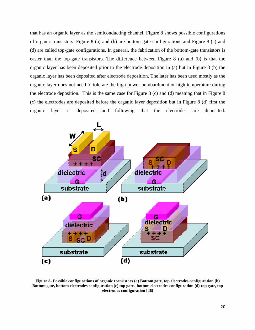
that has an organic layer as the semiconducting channel. Figure 8 shows possible configurations
of organic transistors. Figure 8 (a) and (b) are bottom-gate configurations and Figure 8 (c) and
(d) are called top-gate configurations. In general, the fabrication of the bottom-gate transistors is
easier than the top-gate transistors. The difference between Figure 8 (a) and (b) is that the
organic layer has been deposited prior to the electrode deposition in (a) but in Figure 8 (b) the
organic layer has been deposited after electrode deposition. The later has been used mostly as the
organic layer does not need to tolerate the high power bombardment or high temperature during
the electrode deposition. This is the same case for Figure 8 (c) and (d) meaning that in Figure 8
(c) the electrodes are deposited before the organic layer deposition but in Figure 8 (d) first the
organic layer is deposited and following that the electrodes are deposited.
Figure 8- Possible configurations of organic transistors (a) Bottom gate, top electrodes configuration (b)
Bottom gate, bottom electrodes configuration (c) top gate, bottom electrodes configuration (d) top gate, top
electrodes configuration [46]
Page 22
21
The principle of operation of the organic transistors is similar to the conventional
transistors although some of the aspects of the operation of the organic transistors such as the
contact effect and charge transport are not thoroughly investigated. Moreover the transistor
parameters such as threshold voltage and carrier mobility are not well understood. The thickness
of the organic layer is one of the parameters that affects the device behavior. The effect of the
thickness on the performance can be seen from the contact resistance point, carrier mobility and
the threshold voltage of the transistor. In the remainder of this section the present device theory
regarding the effect of the organic layer thickness on the mobility, contact resistance and
threshold voltage is provided.
The carrier mobility depends on the semiconductor thickness. Specifically in the case of
the pentacene transistors following equation which is proved by [48] implicates that as the layer
thickness increases (“d” in the equation), the carrier mobility also increases. This increment
saturates at a certain thickness called d0. The thickness dependency of the carrier mobility exits
in all OFET structures mentioned earlier.
In the above equation, µsat is the saturation field effect mobility. This equation is the least-square
fit to the experimental results therefore „α‟ is a curve fitting exponent and it can vary depending
on the particular experimental data. [47]
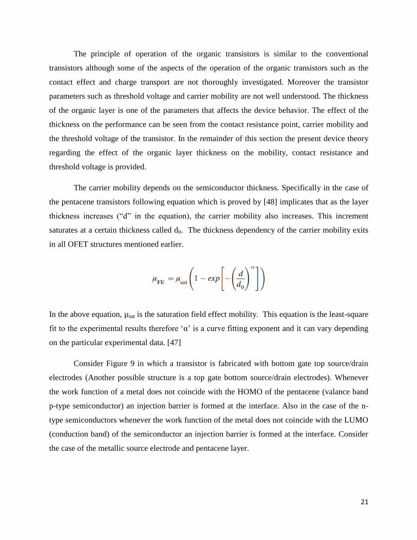
Consider Figure 9 in which a transistor is fabricated with bottom gate top source/drain
electrodes (Another possible structure is a top gate bottom source/drain electrodes). Whenever
the work function of a metal does not coincide with the HOMO of the pentacene (valance band
p-type semiconductor) an injection barrier is formed at the interface. Also in the case of the n-
type semiconductors whenever the work function of the metal does not coincide with the LUMO
(conduction band) of the semiconductor an injection barrier is formed at the interface. Consider
the case of the metallic source electrode and pentacene layer.
Page 23
22
Figure 9 – Bottom gate FET structure with top electrodes [48]
As already mentioned in this section to turn on a transistor the magnitude of the gate-source
voltage should be higher than the threshold voltage. Now assume that the transistor shown above
has a constant drain voltage. If the electric field at the source-semiconductor interface exceeds a
critical value denoted as Ecrit the transistor observes the source-drain current saturation. For
lower source-semiconductor electric field the transistor operates in the sub-linear region. The
following equation shows that the total threshold voltage depends on the ohmic part of source-
semiconductor interface denoted as VT(Ω). VT,inj(t) is the thickness dependent threshold voltage
that is due to the injection barrier. The injection barriers in organic semiconductors are described
later in more details.
In this equation t is the total thickness of the pentacene film and the insulator layer together. εs
and Ecrit are the dielectric constant of the semiconductor and the critical electric field
respectively. The critical electric field is the minimum required electric field for the transistor to
saturate.
As an example in pentacene transistors with the thicknesses ranging from 930nm down to 30nm
(not including the insulator thickness) the threshold voltage range is -2.67 V to -0.67 V.
Schreoder et al. believe that based on the above equation and the experimental results that the
threshold voltage has a linear relation to the film thickness. This means that as the thickness of
the pentacene film decreases the threshold voltage reduces too. [48]
In summary decreasing the film thickness decreases the threshold voltage which is a requirement
for low power applications. On the other hand the thickness reduction decreases the mobility and
speed of operation.
Page 24
23
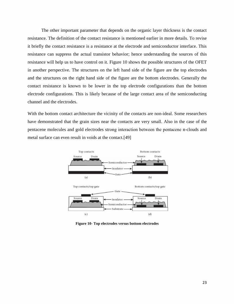
The other important parameter that depends on the organic layer thickness is the contact
resistance. The definition of the contact resistance is mentioned earlier in more details. To revise
it briefly the contact resistance is a resistance at the electrode and semiconductor interface. This
resistance can suppress the actual transistor behavior; hence understanding the sources of this
resistance will help us to have control on it. Figure 10 shows the possible structures of the OFET
in another perspective. The structures on the left hand side of the figure are the top electrodes
and the structures on the right hand side of the figure are the bottom electrodes. Generally the
contact resistance is known to be lower in the top electrode configurations than the bottom
electrode configurations. This is likely because of the large contact area of the semiconducting
channel and the electrodes.
With the bottom contact architecture the vicinity of the contacts are non-ideal. Some researchers
have demonstrated that the grain sizes near the contacts are very small. Also in the case of the
pentacene molecules and gold electrodes strong interaction between the pentacene π-clouds and
metal surface can even result in voids at the contact.[49]
Figure 10- Top electrodes versus bottom electrodes
Page 25
24
1.5 Mechanisms of charge transport and injection in organic semiconductors
In organic materials charge transport occurs by phonon5 assisted hopping of charges
between localized states. The difference between localized and delocalized transport is that in the
former the transport is phonon assisted whereas in the later the transport is limited by phonon
scattering. [51] In quantum mechanics the delocalized state is a state of motion in which a charge
carrier is spread over a whole molecule or crystal. [52] On the other hand the localized state is a
state of motion in which the carrier may be found anywhere within a region of a material of
linear extent smaller than that of the material.[53]
Another important phenomenon in organic devices is the charge injection. Understanding
this phenomenon is crucial in design and fabrication of the organic transistors. The improper
choice of material and device geometry can result in the suppression of the electrical behavior of
the organic compound.
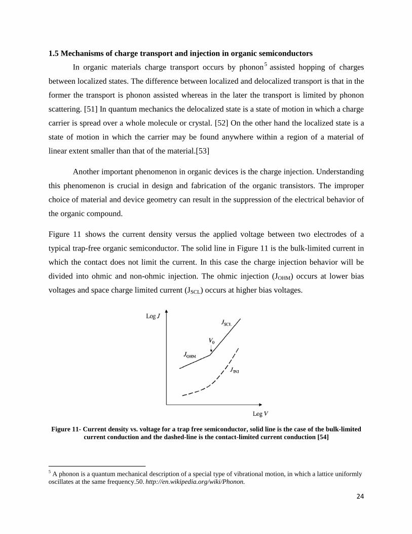
Figure 11 shows the current density versus the applied voltage between two electrodes of a
typical trap-free organic semiconductor. The solid line in Figure 11 is the bulk-limited current in
which the contact does not limit the current. In this case the charge injection behavior will be
divided into ohmic and non-ohmic injection. The ohmic injection (JOHM) occurs at lower bias
voltages and space charge limited current (JSCL) occurs at higher bias voltages.
Figure 11- Current density vs. voltage for a trap free semiconductor, solid line is the case of the bulk-limited
current conduction and the dashed-line is the contact-limited current conduction [54]
5 A phonon is a quantum mechanical description of a special type of vibrational motion, in which a lattice uniformly
oscillates at the same frequency.50. http://en.wikipedia.org/wiki/Phonon.
Page 26
25
Ohmic injection is when the mobility of the free charges in the semiconductor defines the current
limit. In this case free charge motion defines the current limit. The current in this case is defined
by ohms law as shown below.
In the above equation e is the charge of an electron, N0 is the number of the free electrons per
unit volume, µ is the mobility and L is the length.
At higher voltages and electric fields there is a significant increase in charge concentration. This
concentration results a so called Space-Charge Limited (SCL) current and consequently in a non-
linear Ids-Vds characteristic. This type of current conduction is mostly seen in semiconductors
with poor carrier mobility such as organic devices. The low carrier mobility restrains the
collection of the carriers at the electrodes. Also the low carrier mobility increases the possibility
of the recombination of opposite charges. The following equation shows the current density in
space-charge limited regime given by Mott-Gurney law.
In this equation ε and ε0 are the permittivity of the material and the free space permittivity
respectively.
As already mentioned above the solid line in Figure 11 is the bulk-limited current in which the
contact does not limit the current. On the other hand consider the dashed line in the same figure.
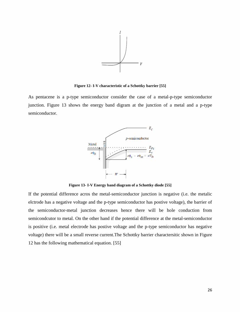
The contact limits the current and this transport mechanism is called injection limited
transport.[54] In this case the energy levels at the interface of organic semiconductor-electrode
define ohmic or non-ohmic injection. Schottky barrier conduction is one of the dominant
behaviors that have been observed in semiconductor-metal junction. This barrier results in non-
ohmic injection hence non-linear current-voltage characteristic. Figure 12 shows the typical I-V
characteristic of a Schottky barrier.
Page 27
26
Figure 12- I-V characteristic of a Schottky barrier [55]
As pentacene is a p-type semiconductor consider the case of a metal-p-type semiconductor
junction. Figure 13 shows the energy band digram at the junction of a metal and a p-type
semiconductor.
Figure 13- I-V Energy band diagram of a Schottky diode [55]
If the potential difference acros the metal-semiconductor junction is negative (i.e. the metalic
elctrode has a negative voltage and the p-type semiconductor has postive voltage), the barrier of
the semiconductor-metal junction decreases hence there will be hole conduction from
semicondcutor to metal. On the other hand if the potential difference at the metal-semiconductor
is positive (i.e. metal electrode has postive voltage and the p-type semiconductor has negative
voltage) there will be a small reverse current.The Schottky barrier charactersitic shown in Figure
12 has the following mathematical equation. [55]
Page 28
27
Consider the last line of the equation. The current in the diode has a dependency on the area of
the diode (A). The parameters T, R* and KB are temperature, Richardson and Boltzman
constants respectively. The parameter eφb is the energy difference between the Fermi level of the
metal and the conduction band of the semicondcutor in the case of an n-type semiconductor. In
the case of the p-type semiconductor this parameter is the energy difference between the Fermi
level of the metal and the valance band of the semiconductor at the junction.
Most of the Schottky barriers (including the Schottky barriers made of inorganic
semiconductors) have low forward bias (i.e. up to 2 V) which makes it popular to be used as low
power devices. One of the applications of the Schottky diode is to be used as a protector at the
input of other modules. As an example the Schottky diode, rather than the Zener diode, has been
used in ADCs to protect them from current runaway. Another application is to be used as the
mixers and detectors in the communication systems. The non-linear behavior of this type of
diode allows system designers to combine different input levels with different weighing ratios
and also on the receiver side (RX) to distinguish them. Another application of the Schottky
behavior is to be used in PhotoVoltaic(PV) systems. Low forward voltage conduction and high
carrier densities in the semiconductor side results in easy current flow through the layers.[56]
Page 29
28
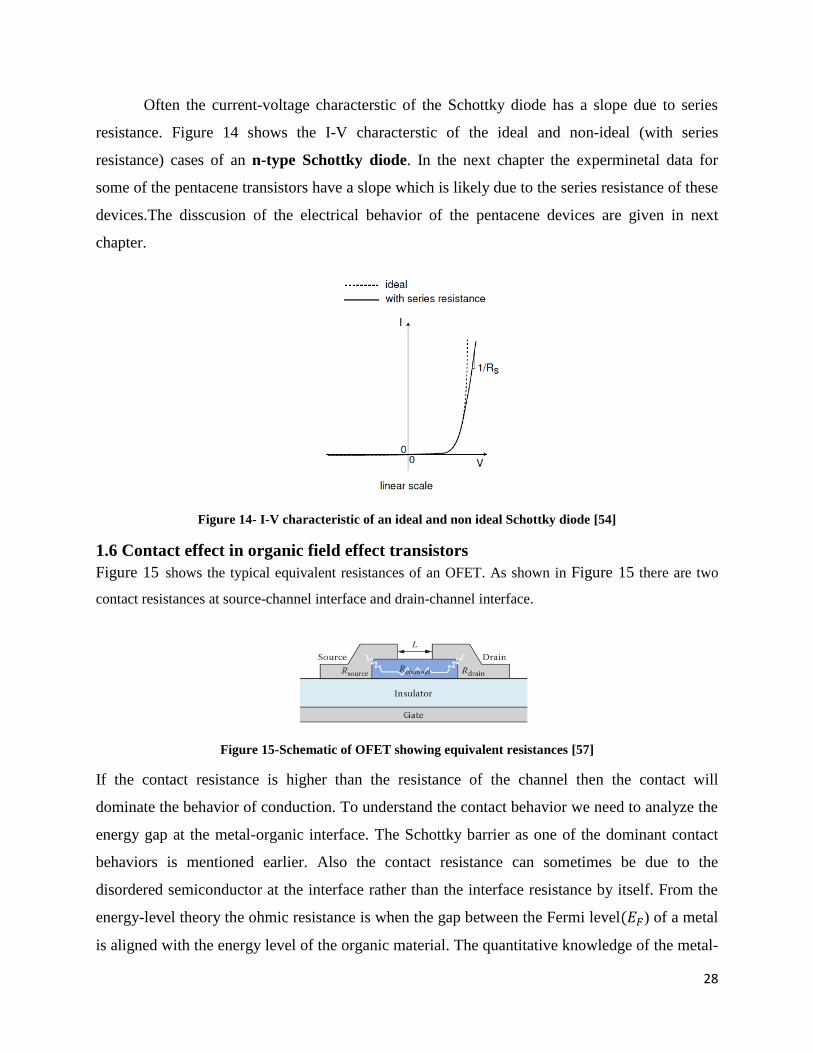
Often the current-voltage characterstic of the Schottky diode has a slope due to series
resistance. Figure 14 shows the I-V characterstic of the ideal and non-ideal (with series
resistance) cases of an n-type Schottky diode. In the next chapter the experminetal data for
some of the pentacene transistors have a slope which is likely due to the series resistance of these
devices.The disscusion of the electrical behavior of the pentacene devices are given in next
chapter.
Figure 14- I-V characteristic of an ideal and non ideal Schottky diode [54]
1.6 Contact effect in organic field effect transistors
Figure 15 shows the typical equivalent resistances of an OFET. As shown in Figure 15 there are two
contact resistances at source-channel interface and drain-channel interface.
Figure 15-Schematic of OFET showing equivalent resistances [57]
If the contact resistance is higher than the resistance of the channel then the contact will
dominate the behavior of conduction. To understand the contact behavior we need to analyze the
energy gap at the metal-organic interface. The Schottky barrier as one of the dominant contact
behaviors is mentioned earlier. Also the contact resistance can sometimes be due to the
disordered semiconductor at the interface rather than the interface resistance by itself. From the
energy-level theory the ohmic resistance is when the gap between the Fermi level ) of a metal
is aligned with the energy level of the organic material. The quantitative knowledge of the metal-
Page 30
29
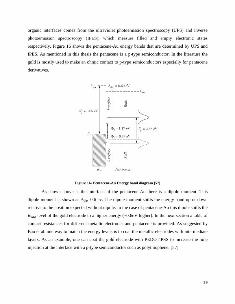
organic interfaces comes from the ultraviolet photoemission spectroscopy (UPS) and inverse
photoemission spectroscopy (IPES), which measure filled and empty electronic states
respectively. Figure 16 shows the pentacene-Au energy bands that are determined by UPS and
IPES. As mentioned in this thesis the pentacene is a p-type semiconductor. In the literature the
gold is mostly used to make an ohmic contact to p-type semiconductors especially for pentacene
derivatives.
Figure 16- Pentacene-Au Energy band diagram [57]
As shown above at the interface of the pentacene-Au there is a dipole moment. This
dipole moment is shown as Δdip=0.6 ev. The dipole moment shifts the energy band up or down
relative to the position expected without dipole. In the case of pentacene-Au this dipole shifts the
level of the gold electrode to a higher energy (~0.6eV higher). In the next section a table of
contact resistances for different metallic electrodes and pentacene is provided. As suggested by
Bao et al. one way to match the energy levels is to coat the metallic electrodes with intermediate
layers. As an example, one can coat the gold electrode with PEDOT:PSS to increase the hole
injection at the interface with a p-type semiconductor such as polythiophene. [57]
Page 31
30
1.7 Contact resistance extraction and measurement methods
The contact resistance found using simple I-V measurements may not be accurate in organic
devices. There are methods to extract or measure the contact resistance in organic transistors. In
the next sections three methods that have been reported and used in the literature are mentioned.
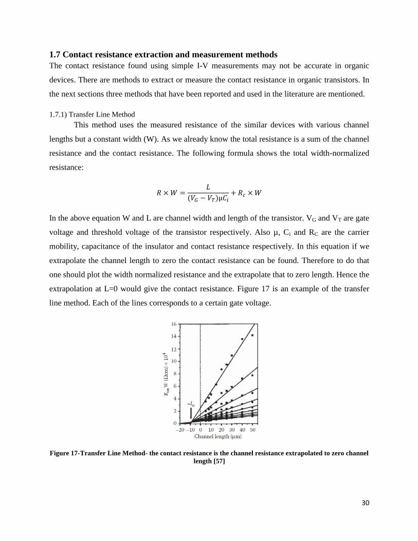
1.7.1) Transfer Line Method
This method uses the measured resistance of the similar devices with various channel
lengths but a constant width (W). As we already know the total resistance is a sum of the channel
resistance and the contact resistance. The following formula shows the total width-normalized
resistance:
In the above equation W and L are channel width and length of the transistor. VG and VT are gate
voltage and threshold voltage of the transistor respectively. Also µ, Ci and RC are the carrier
mobility, capacitance of the insulator and contact resistance respectively. In this equation if we
extrapolate the channel length to zero the contact resistance can be found. Therefore to do that
one should plot the width normalized resistance and the extrapolate that to zero length. Hence the
extrapolation at L=0 would give the contact resistance. Figure 17 is an example of the transfer
line method. Each of the lines corresponds to a certain gate voltage.
Figure 17-Transfer Line Method- the contact resistance is the channel resistance extrapolated to zero channel
length [57]
Page 32
31
This method has several drawbacks. The most important drawback is that the equation written
above assumes an ohmic contact; therefore in the case of a non-linear contact resistance that
equation is no longer valid. Another major drawback is that this method cannot distinguish the
contact resistance at the drain interface and source interface. Other drawbacks are the need of
fabrication of several devices and minimize the variation of the coating in all devices. [58]
1.7.2) Four Probe Measurements
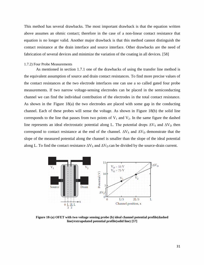
As mentioned in section 1.7.1 one of the drawbacks of using the transfer line method is
the equivalent assumption of source and drain contact resistances. To find more precise values of
the contact resistances at the two electrode interfaces one can use a so called gated four probe
measurements. If two narrow voltage-sensing electrodes can be placed in the semiconducting
channel we can find the individual contribution of the electrodes in the total contact resistance.
As shown in the Figure 18(a) the two electrodes are placed with some gap in the conducting
channel. Each of these probes will sense the voltage. As shown in Figure 18(b) the solid line
corresponds to the line that passes from two points of V1 and V2. In the same figure the dashed
line represents an ideal electrostatic potential along L. The potential drops ∆VS and ∆VD then
correspond to contact resistance at the end of the channel. ∆VS and ∆VD demonstrate that the
slope of the measured potential along the channel is smaller than the slope of the ideal potential
along L. To find the contact resistance ∆VS and ∆VD can be divided by the source-drain current.
Figure 18-(a) OFET with two voltage sensing probe (b) ideal channel potential profile(dashed
line)/extrapolated potential profile(solid line) [57]
Page 33
32
1.7.3) Kelvin Probe Force Microscopy
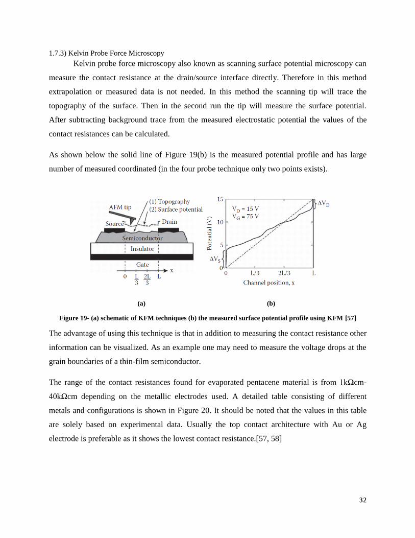
Kelvin probe force microscopy also known as scanning surface potential microscopy can
measure the contact resistance at the drain/source interface directly. Therefore in this method
extrapolation or measured data is not needed. In this method the scanning tip will trace the
topography of the surface. Then in the second run the tip will measure the surface potential.
After subtracting background trace from the measured electrostatic potential the values of the
contact resistances can be calculated.
As shown below the solid line of Figure 19(b) is the measured potential profile and has large
number of measured coordinated (in the four probe technique only two points exists).
(a) (b)
Figure 19- (a) schematic of KFM techniques (b) the measured surface potential profile using KFM [57]
The advantage of using this technique is that in addition to measuring the contact resistance other
information can be visualized. As an example one may need to measure the voltage drops at the
grain boundaries of a thin-film semiconductor.
The range of the contact resistances found for evaporated pentacene material is from 1kΩcm-
40kΩcm depending on the metallic electrodes used. A detailed table consisting of different
metals and configurations is shown in Figure 20. It should be noted that the values in this table
are solely based on experimental data. Usually the top contact architecture with Au or Ag
electrode is preferable as it shows the lowest contact resistance.[57, 58]
Page 34
33
Figure 20- Evaporated Pentacene – Measured contact resistance for various metallic electrodes [57]
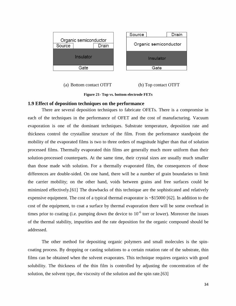
1.8 Top contact vs. bottom contact FETs
In this thesis the bottom gated configuration is used due to ease of fabrication. In the case
of the bottom gated configuration the source and drain electrodes can be deposited before or after
organic layer coating, leading to the bottom and top electrode configurations. In the bottom
electrode configuration the electrodes are patterned and following that the organic layer is
deposited. On the other hand in the top contact configuration the electrodes are deposited after
organic layer coating. There are a few differences in performance. In the bottom contact
configuration there is a thickness variation near the electrodes. In the top contact configuration
there is a uniform contact between the electrodes and semiconductor. This results in a lower
contact resistance and efficient charge injection.[59] Moreover in the circuit applications the top
contact FETs give higher gain-bandwidth product due to reduced gate-drain capacitance. As the
gate-drain capacitance is inversely proportional to distance between the gate and drain
electrodes, the overall capacitance will decrease. [60] In this thesis as will be discussed in more
details later in chapter 2, the bottom contact fabrication method is chosen due to simplicity of the
fabrication process. Note that both configurations shown in Figure 21 use the bottom gated
configuration in which the wafer is used as the actuating (gate) electrode. One may also use these
structures in conjunction with a top-gate electrode. In this case following the fabrication of the
bottom/top electrodes configuration a layer of an insulator will be deposited. After that the gate
electrode will be deposited on top of the insulator layer.
Page 35
34
(a) Bottom contact OTFT (b) Top contact OTFT
Figure 21- Top vs. bottom electrode FETs
1.9 Effect of deposition techniques on the performance
There are several deposition techniques to fabricate OFETs. There is a compromise in
each of the techniques in the performance of OFET and the cost of manufacturing. Vacuum
evaporation is one of the dominant techniques. Substrate temperature, deposition rate and
thickness control the crystalline structure of the film. From the performance standpoint the
mobility of the evaporated films is two to three orders of magnitude higher than that of solution
processed films. Thermally evaporated thin films are generally much more uniform than their
solution-processed counterparts. At the same time, their crystal sizes are usually much smaller
than those made with solution. For a thermally evaporated film, the consequences of those
differences are double-sided. On one hand, there will be a number of grain boundaries to limit
the carrier mobility; on the other hand, voids between grains and free surfaces could be
minimized effectively.[61] The drawbacks of this technique are the sophisticated and relatively
expensive equipment. The cost of a typical thermal evaporator is ~$15000 [62]. In addition to the
cost of the equipment, to coat a surface by thermal evaporation there will be some overhead in
times prior to coating (i.e. pumping down the device to 10-6
torr or lower). Moreover the issues
of the thermal stability, impurities and the rate deposition for the organic compound should be
addressed.
The other method for depositing organic polymers and small molecules is the spin-
coating process. By dropping or casting solutions to a certain rotation rate of the substrate, thin
films can be obtained when the solvent evaporates. This technique requires organics with good
solubility. The thickness of the thin film is controlled by adjusting the concentration of the
solution, the solvent type, the viscosity of the solution and the spin rate.[63]
Page 36
35
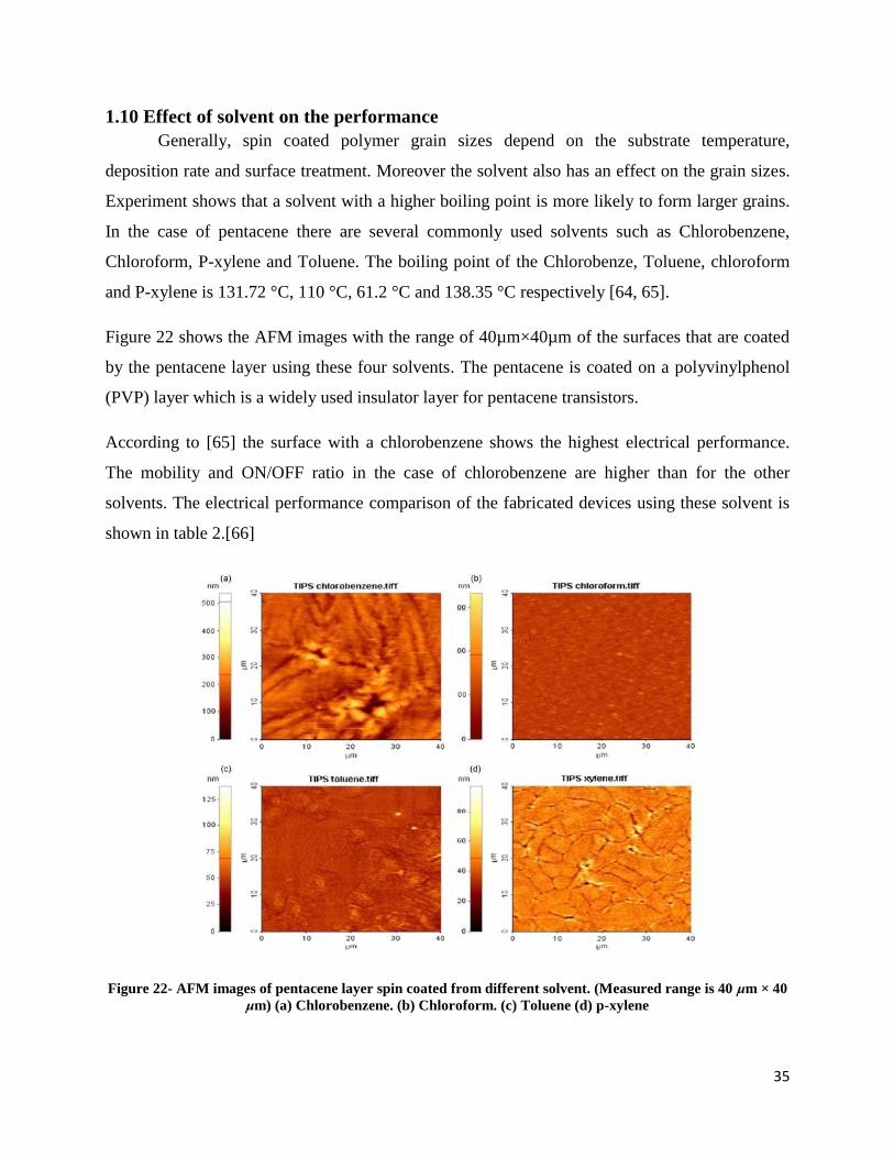
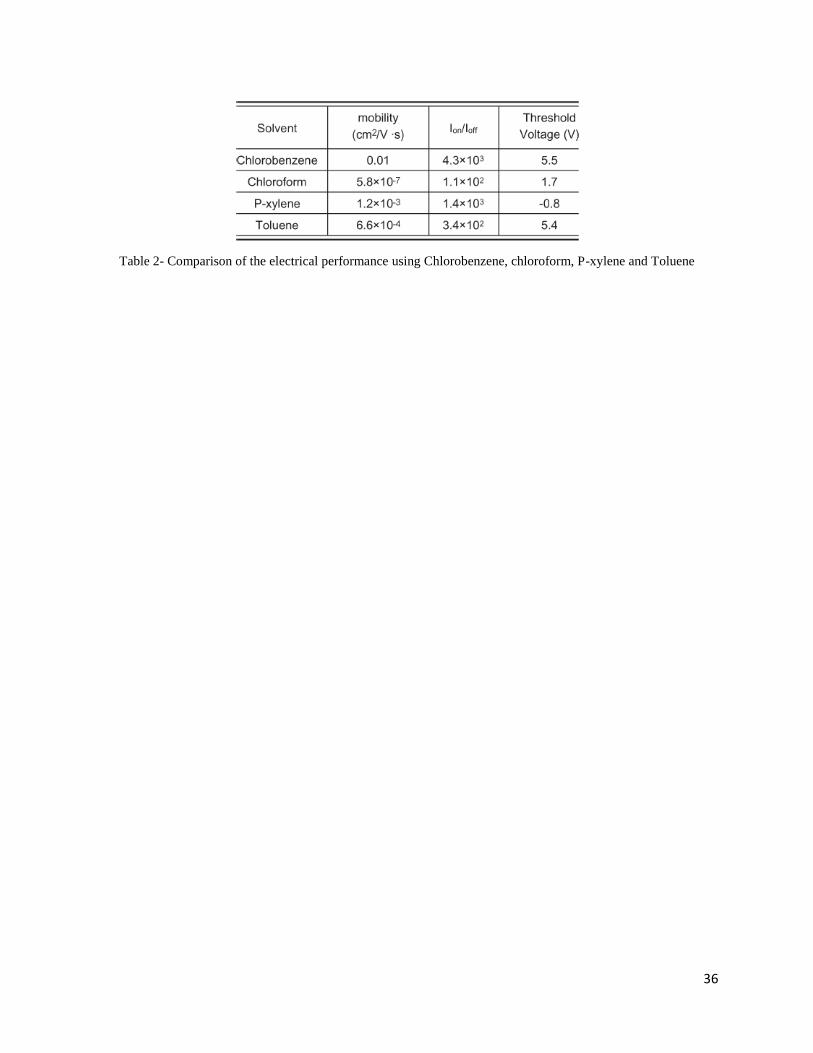
1.10 Effect of solvent on the performance
Generally, spin coated polymer grain sizes depend on the substrate temperature,
deposition rate and surface treatment. Moreover the solvent also has an effect on the grain sizes.
Experiment shows that a solvent with a higher boiling point is more likely to form larger grains.
In the case of pentacene there are several commonly used solvents such as Chlorobenzene,
Chloroform, P-xylene and Toluene. The boiling point of the Chlorobenze, Toluene, chloroform
and P-xylene is 131.72 °C, 110 °C, 61.2 °C and 138.35 °C respectively [64, 65].
Figure 22 shows the AFM images with the range of 40µm×40µm of the surfaces that are coated
by the pentacene layer using these four solvents. The pentacene is coated on a polyvinylphenol
(PVP) layer which is a widely used insulator layer for pentacene transistors.
According to [65] the surface with a chlorobenzene shows the highest electrical performance.
The mobility and ON/OFF ratio in the case of chlorobenzene are higher than for the other
solvents. The electrical performance comparison of the fabricated devices using these solvent is
shown in table 2.[66]
Figure 22- AFM images of pentacene layer spin coated from different solvent. (Measured range is 40 μm × 40
μm) (a) Chlorobenzene. (b) Chloroform. (c) Toluene (d) p-xylene
Page 37
36
Table 2- Comparison of the electrical performance using Chlorobenzene, chloroform, P-xylene and Toluene
Page 38
37
Chapter 2 – Fabrication and Characterization of OFETs
2.1 Device Fabrication Procedure
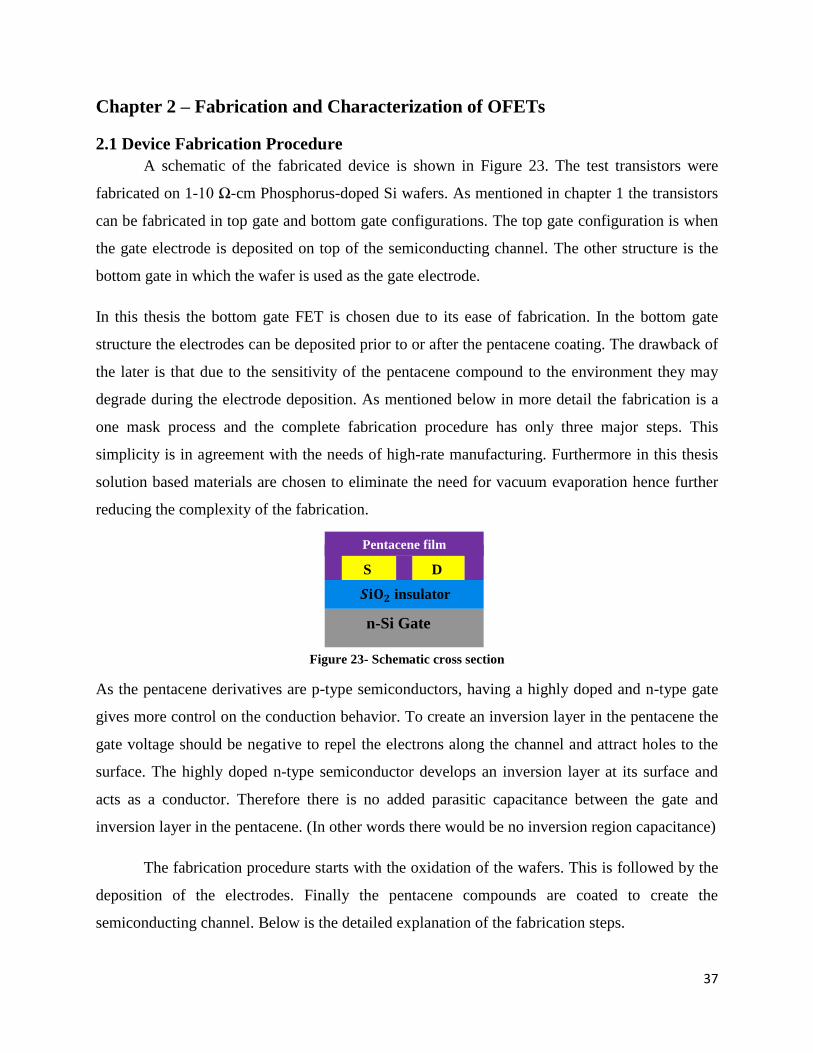
A schematic of the fabricated device is shown in Figure 23. The test transistors were
fabricated on 1-10 Ω-cm Phosphorus-doped Si wafers. As mentioned in chapter 1 the transistors
can be fabricated in top gate and bottom gate configurations. The top gate configuration is when
the gate electrode is deposited on top of the semiconducting channel. The other structure is the
bottom gate in which the wafer is used as the gate electrode.
In this thesis the bottom gate FET is chosen due to its ease of fabrication. In the bottom gate
structure the electrodes can be deposited prior to or after the pentacene coating. The drawback of
the later is that due to the sensitivity of the pentacene compound to the environment they may
degrade during the electrode deposition. As mentioned below in more detail the fabrication is a
one mask process and the complete fabrication procedure has only three major steps. This
simplicity is in agreement with the needs of high-rate manufacturing. Furthermore in this thesis
solution based materials are chosen to eliminate the need for vacuum evaporation hence further
reducing the complexity of the fabrication.
Figure 23- Schematic cross section
As the pentacene derivatives are p-type semiconductors, having a highly doped and n-type gate
gives more control on the conduction behavior. To create an inversion layer in the pentacene the
gate voltage should be negative to repel the electrons along the channel and attract holes to the
surface. The highly doped n-type semiconductor develops an inversion layer at its surface and
acts as a conductor. Therefore there is no added parasitic capacitance between the gate and
inversion layer in the pentacene. (In other words there would be no inversion region capacitance)
The fabrication procedure starts with the oxidation of the wafers. This is followed by the
deposition of the electrodes. Finally the pentacene compounds are coated to create the
semiconducting channel. Below is the detailed explanation of the fabrication steps.
n-Si Gate
insulator
S D
Pentacene film
Page 39
38
1. Oxidation of wafers
Prior to oxidation the wafers are cleaned using 10 minutes of piranha (H2SO4:H2O2 2:1 at 105°C
-115°C) to remove the organic residues followed by a rinse using deionized (DI) water. After the
rinse step the resistivity of water is measured automatically which shows a resistance higher than
1MΩ-cm. The concentration of the sulfuric acid and hydrogen peroxide used for the Piranha etch
is 96% and 30% respectively. The next step is 15 seconds in hydrofluoric (HF) acid followed by
a rinse as well as 10 minutes of hydrochloric acid/H2O2 bath to remove the metallic residues. The
HF concentration is 49 % with the ratio of 50 DI water to 1 HF. Also the concentration of HCL
is 37% with 6:1:1 ratio of DI water, HCL and hydrogen peroxide. The concentration of the
hydrogen peroxide is 30%. This clean process takes approximately 30 minutes. The last step is to
rinse and dry the wafers. The rinse is a rotation of the wafers at 1500 rpm for 150 seconds and
the dry is with nitrogen in the rinser-dryer for 300 seconds.
The clean procedure mentioned above is the so called a pre-diffusion clean and is a necessary
step to remove the particles and contamination hence increasing the yield of the devices. After
the clean step the wafers should be loaded immediately in the quartz boat for the oxidation step.
If the wafers are left in the air there will be a very thin-layer (few angstrom) of oxide formation.
In addition the wafers that are left in the air can absorb moisture and other residues hence
reducing the yield of the devices.
The gate insulator is 500 nm thermally grown SiO2. This insulator was grown using wet
oxidation and it took 35 minutes at 1100°C in a horizontal furnace not including the temperature
ramp up. The furnace is programmed to have 10 minutes temperature ramp-up in nitrogen. In the
case of the wet oxidation after temperature ramp-up the water valve of the furnace should be
open.
To be more specific the boat loader push and pull time was programmed to be 12 minutes. After
the boat loader push (meaning the wafers are inside the furnace and ready for the oxidation) the
temperature ramp up takes place for 10 minutes. Following the oxidation time there will be 10
minutes temperature ramp down. The oxidation step will be completed after this step.
Page 40
39
2. Electrodes patterning and lift-off
Prior to depositing the electrodes the wafers are coated by photoresist (PR) AZ1813. This
photoresist is spun coated at 4000rpm and baked for 1 minute at 115°C. Following the PR
coating the UV exposure is done for 6.5 seconds using the Quintel 4000 mask aligner. The UV
power supply should be set to 60 V. The image of the mask used for the fabrication of the
organic transistor is shown in Figure 24. The devices close to the border of the mask are the
devices used to fabricate transistors. This mask was designed by former students and provided to
me for this project. The devices located close to the center of the mask are the micropumps and
they do not have any significance for our application. The transistors‟ electrodes have
considerable area (meaning the electrodes are unnecessary large). The drawback of such an area
is that upon the existence of any oxide pinhole underneath, the device will have a leakage hence
will be malfunction.
Figure 24- mask used for the fabrication of OFETs
The next step after exposure is to develop the wafers in MIF319 developer for 45 seconds. The
source/drain electrodes were 150 nm Au with a 30 nm Cr adhesion layer, deposited by
magnetron sputtering and patterned by lift-off. The substrate temperature was not measured but
is believed to be 45-50°C. The DC power during the Cr deposition is 165 W for 30 seconds and
Page 41
40
the RF power during the Au deposition is 500 W for 4 minutes and 30 seconds. The pressure of
the system prior to deposition was
As AZ1813 is a positive photoresist the lift-off process is by immersing the wafers in the
Acetone bath for approximately 30 minutes. For feature sizes less than 10µm the lift-off process
needs more force. An acetone spray bottle helps to remove the photoresist for small feature.
To achieve a good electrical contact to the silicon wafer that is used as the gate electrode, the
oxide on the back side of the wafer was removed using 10:1 Buffered Oxide Etch (BOE). The
total etch time is 7 minutes to remove 500nm silicon dioxide. The etch rate of the BOE is 100 nm
per minute (100nm×5min=500nm oxide etch). The 2 minutes over etch is done to make sure that
the back side of the wafer is completely free from oxide. To protect the patterned electrodes
during the oxide etch the front side of the wafer is coated by photoresist AZ1813. In this case
any thick photoresist can be used and as AZ1813 will give approximately 1.3µm layer it is a
good choice for protection of the polished side.
3. Pentacene coating and anneal
Prior to pentacene coating the substrates and electrodes were cleaned using piranha etch
(H2SO4:H2O2 2:1 at 115°C) for 10 minutes. The concentration of the reagents is same as for the
pre-diffusion clean mentioned earlier. The reason for the piranha etch is to remove any possible
organic residue.
To improve the adhesion of the pentacene layer, a self assembled monolayer of
hexamethyldisilazane (HMDS) was first spin coated on the wafer at 4000 rpm and baked at
150°C for 5 min. The pentacene solutions were spin coated at 1500 rpm for 1 minute followed
by a 60°C hot plate bake for 1 minute in atmosphere. All the solutions were 2 wt% pentacene in
Toluene solvent.
In this thesis five derivatives of pentacene were characterized. These materials were synthesized
at the department of chemistry of University of New Hampshire (UNH) with the supervision of
Dr. Glen Miller and Dr. Irvinder Kaur. The synthesized compounds were given to us for
electrical characterization. The main aim of this thesis is to understand the behavior of organic
FETs, conduction mechanisms and their limitations on electrical performance. The following
Page 42
41
table shows the chemical names and structure of the derivatives. All of these compounds are
photo-oxidization resistant and are thermally stable compared with TIPS pentacene.
Compound Chemical Name Structure
1
6,13-Bis(phenethylthio)pentacene
2
2,3,9,10-Tetrachloro-6,13-
bis(phenethylthio)pentacene
3
6,13-Bis(4'-methoxyphenethylthio)pentacene
4
6,13-Bis(2',3',4',5',6'-
pentaflourophenethylthio)pentacene
5
6,13-dichloropentacene
Table 3- Pentacene compounds used in this thesis
Page 43
42
2.2 Thin-film properties and thickness measurements
For the 2,3,9,10-Tetrachloro-6,13-bis(phenethylthio)pentacene, the spin coating process
resulted in a thin-film of pentacene with an overall thickness of approximately 20nm.A SEM
image of this device is shown in Figure 25. The thin-film of pentacene has grain sizes of few
microns. This compound does not have any scattered crystals and only the thin layer of
pentacene film is present. To measure the thickness, the film was scratched to the silicon dioxide
layer with a sharp razor. Following that the Dektak was used to measure the thickness of the
film. The Dektak is a surface profile measuring instrument. Particularly the Dektak3ST is the
equipment used for this project that has a vertical range of 100Å-1310KÅ. [67] Surprisingly the
film thickness of 20 nm was varied by only +/- 2 nm over a 50 μm scan. In the next section the
electrical characteristic of the materials are discussed in more detail and in the case of this
compound reasonable transistor characteristics similar to the conventional transistor have been
observed.
Figure 25- SEM image of the device with channel dimension of W=2000µm, L=10 µm. The large light
rectangles are the electrodes (with electrical connections to the right and left), and the irregular material is
the deposited “2,3,9,10-Tetrachloro-6,13-bis(phenethylthio)pentacene” after spin coating and baking
For the 6,13-Bis(phenethylthio) pentacene, the film was approximately 150 nm thick. The
optical micrograph of this compound is shown in Figure 26. The thickness was again measured
using the Dektak by scratching the film. This micrograph also shows the existence of the
scattered crystals in addition to the film for this compound. These crystals exist in three out of
the five derivatives of pentacene mentioned in this thesis. To get a uniform film the evaporation
of the compounds is also possible if the compound is thermally stable. It is worth mentioning
that the compounds in this thesis are thermally stable and evaporation of them can be done at
Page 44
43
relatively low temperature (<400ºC). Unfortunately the thermal evaporator was under repair
during the course of the project.
.
Figure 26- 6,13-Bis(phenethylthio) pentacene –optical micrograph
Figure 27 shows the devices fabricated with 6,13-Bis(4'-methoxyphenethylthio)
pentacene. The figure shows the exsitance of the scattterd crystals all over the channel as well as
the electrodes. For the 6,13-Bis(4'-methoxyphenethylthio) pentacene a 200 nm film was present.
Although the solution concentration is same for all the compounds the density of the scattered
crystals on the surface varies. This particular compound shows the highest density of crystals on
the wafer.
Figure 28 shows the devices fabricated with 6,13-Bis(2',3',4',5',6'-pentaflourophenethylthio)
pentacene. The randomly distributed crystals are apparent in these devices too. Also a very thin
layer of 20nm film is present over the wafer.
As already mentioned in the fabrication section the silicon dioxide thickness is 500 nm. From the
color chart of the silicon dioxide this thickness has green-blue color. Looking at the figures the
surface color of the wafers are not green-blue. This also confirms that in addition to the scattered
crystals that are apparent on the surface there is a layer that changes the color of the wafer.
Page 45
44
Figure 27- 6,13-Bis(4'-methoxyphenethylthio)pentacene
Figure 28-6,13-Bis(2',3',4',5',6'-pentaflourophenethylthio)pentacene
The last compund is the 6,13-dichloropentacene shown in Figure 29. The image shows a
non-uniform coating of material which has the average thickness of 200 nm. The thickness
measurement is done again using Dektak by scratching the thin layer of pentacene. This
compound does not have scattered crystals and is one of the compounds that show transistor
behavior similar to the conventional transistors.
Page 46
45
Figure 29-6,13-dichloropentacene
2.3 I-V measurements
To find the electrical characteristic of these organic compounds we use standard current-
voltage measurements. As already shown in the above figures these compounds are coated
between two electrodes. Applying voltage and measuring the current passing between these
electrodes shows the electrical behavior of these materials. The gate electrode (in this case the
wafer itself) is used to alter the conducting channel. Three of the compounds show transistor
behavior similar to the conventional transistors. The other compounds show different types of
electrical characteristics. Some of the possible reasons these behaviors are discussed later in this
report.
The I-V measurements are done using semiconductor parameter analyzer HP4155A in a dark
environment at room temperature. The gate voltage is applied with the SMU (Source Measure
Unit) from the parameter analyzer to the chuck of the probe station. To make sure that the wafer
is in a good contact with the chuck the chuck pump is running during the measurements. The
drain voltage is applied through the other SMU while the source is grounded. The data is
gathered with a LabView version 8.6 program connected to the semiconductor parameter
analyzer.
2.3.1) Parameter extraction from experiments
As already mentioned the drain current depends on two voltages, the drain voltage and
the gate voltage. Therefore the I-V data can be plotted as either an output characteristic or a
transfer characteristic. The output characteristic is when the drain current is plotted versus drain
voltage for various gate voltages and the transfer characteristic is when the drain current is
Page 47
46
plotted versus gate voltage for a particular drain voltage. For the transfer characteristic the
chosen drain voltage can be a low value such that the transistor operates in the triode region or
high enough value that the transistor operates in the saturation region. In the linear region (low
voltage part of the triode region) the charge distribution along the channel is uniform but in the
saturation region this uniformity is not present anymore. In this case an exact estimate of the
carrier mobility requires an integration of the saturation current along the channel which is not
easily feasible. Therefore the mobility calculation in the linear region is mostly preferred. This is
the case for the conventional transistors.
In the case of our measurements the linear region suffers from the contact resistance. This
resistance can be noticed from a slope of Ids-Vds data at low drain-source voltages. This
phenomenon is discussed in more detail later in this chapter. Due to this resistance seen in our
measurements the mobility extraction is done using the saturation part of the Ids-Vds curve. This
results in more accurate parameter extraction.
To extract the mobility and threshold voltage from the experimental graph we need to use the
mathematical approximation to match the experimental data with the theoretical formula. One of
the problems of extracting the parameters in organic FETs is the lack of a complete model. A
complete model means that the model should be able to explain the electrical behavior of the
organic transistor thoroughly. Consequently most of the calculation is based on the standard long
channel FETs. The reason for choosing the long channel model is that the minimum channel
length fabricated in this project is 10µm. It should be considered that there are two assumptions
for the long channel model, one is the gradual channel approximation and the other is the
constant carrier mobility. Both of these assumptions are addressed in chapter 1 in more detail.
Also carrier mobility in organic FETs has been reported to depend on the gate voltage which
makes the parameter extraction more difficult. [68] In this thesis the parameter are extracted
based on the long channel FET equations and assuming a gate voltage independent mobility. In
this method the Ids versus Vg is plotted at high Vds (the drain-source voltage should be high
enough for the transistor to operate in the saturation region). The curvature at low Vds cannot be
used to retrieve the carrier mobility as this region is dominated by the contact conduction. Figure
30 shows a typical Ids-Vg curve. The numbers on the axes of the figure have no significance and
they are for the demonstration of the concept.
Page 48
47
To find the threshold voltage we need to extrapolate the highest slope of the curve to zero drain-
source current. [69]
Figure 30- Mobility extraction using extrapolation [69]
Following that using the equation mentioned below the carrier mobility can be extracted as:
This equation is derived from the current-voltage equation in saturation region which is proved
earlier in chapter 1.
2.3.2) Experimental I-V measurements
2.3.2.1) 2,3,9,10-Tetrachloro-6,13-bis(phenethylthio) pentacene
The drain current as a function of drain voltage for different gate voltages is shown in
Figure 31(a). This device is behaving as a p-channel Field Effect Transistor. As it is expected
the conduction of the channel increases as the magnitude of the gate-source voltage increases.
Also if the gate-source voltage increases to a value more than -2 V the transistor turns off.
Figure 31(b) shows the drain current versus gate-source voltage at . The reason for
this value of drain-source voltage is that the transistor should operate well within saturation
region for more reliable parameter extraction.
Page 49
48
The left axis corresponds to a plot (blue) of versus Vgs. Using the straight part of this curve
extrapolated to zero current, the threshold voltage is found to be -1.8V. Also assuming a gate-
voltage independent mobility and using the W/L ratio of the electrodes (for this particular device
is 2000µm/10µm), the field effect mobility is 0.0035 cm2/V·s. This value is found using the
straight portion of the versus Vgs curve and the equation mentioned in the previous section
for FETs in the saturation region. Section 2.3.1 explained the extraction method used here in
more detail. From the right axis (red curve) of Figure 31(b) the On/Off current ratio of this
device is seen to be 104. This value is calculated by taking the ratio of the drain current
(logarithmic scale) at the gate-source voltages of -15V and +40V.
(a) (b)
Figure 31 - (a) Drain current vs. drain-source voltage for several gate voltages (W=2000µm, L=10 µm) (b)
square root and log of Drain Current vs. gate-source voltage. This device has a field-effect hole mobility of
0.0035
, Vt=-1.8 V and an on/off current ratio of 10
4.
Figure 32 shows the simulated IV characteristic of this compound as well as the measured data.
The simulation for the standard FET is done using parameters that are extracted above and long
channel transistor model. In the simulation the aspect ratio of this device is 200 and as the
insulator thickness is 500 nm the oxide capacitance is
. As shown in the figure the
simulated data does not perfectly match the experimental data. Some of the reasons for this
imperfect match are discussed below.
Page 50
49
Figure 32- Experimental data and standard transistor behavior of 2,3,9,10-Tetrachloro-6,13-
bis(phenethylthio)pentacene
In general, the contacts may have a large resistance and may have non-linear I-V characteristics.
The non-linear behavior at low drain-source voltages in all the devices, including in the transistor
characteristic of Figure 31(a), is thought to be caused by contact effect.
Also If the material being tested has a significant bulk conductivity, the shunt resistance may be
low enough that the transistor characteristic obscured by the current flowing through the bulk of
the material. This phenomenon can be seen as the slope of the I-V curve when the transistor
operates in the saturation region. The transistor characteristic shown in Figure 31, 33 and 37 has
this effect of bulk conductivity.
2.3.2.2) 6,13-Bis(2',3',4',5',6'-pentaflourophenethylthio) pentacene
Figure 33 shows the charcaterisc of 6,13-Bis(2',3',4',5',6'-pentaflourophenethylthio)
pentacene. This characteristic also shows a p-channel FETs behavior with contact effects. The
contact effect is shown as a curvature at low Vds. Also the slope of the curve at the saturation
region of Figure 33 suggests the existance of shunt resistance. As Vg decreases - in this case
below -5 Volts - the contact resistance becomes dominant rather than the actual FET behavior.
Using the same method described above, the mobility and threshold voltage are found to be
and -1.66 V repectively. The aspect ratio of the electrodes for this device is
Page 51
50
also 2000 µm/10µm. As already mentioned in section 2.2 this compund forms a thin film of 20
nm wih scattered crystalls spreading on the surface.
(a) (b)
Figure 33-FET behavior with contact effect of 6,13-Bis(2',3',4',5',6'-pentaflourophenethylthio) pentacene
(a) Negative Vds sweep (b) Positive Vds Sweep
Figure 34 shows the simulated behavior of a standard MOSFET with the extracted parameter as
well as the experimental data. As already mentioned the MOSFET model does not include all
aspects of the conduction behavior in the organic transistors. Therefore the model will not fit the
measured data as well as it would for a conventional transistor.
Figure 34-Experimental data of 6,13-Bis(2',3',4',5',6'-pentaflourophenethylthio) pentacene and standard
MOSFET behvior with the extracted parametrs
Page 52
51
2.3.2.3) 6,13-Bis (4'-methoxyphenethylthio) pentacene & 6,13-Bis(phenethylthio) pentacene
Figure 35 and 36 show Ids versus source-drain sweep of 6,13-
Bis(phenethylthio)pentacene and 6, 13-Bis(4'-methoxyphenethylthio)pentacene. Clearly the
behavior is not a standard transistor characteristic. The standard transistor characteristic has
distinguishable ON and OFF states. These figures show that the conduction varies as the gate
voltage changes but it is unlikely that these devices go to the OFF state. Later in this section the
parasitic effects and the reasons for deviation from conventional FET characteristic are
discussed. As mentioned above, these two compounds each have a 150-200 nm film and in
addition have randomly distributed crystals. The crystals are typically a few micrometers long.
The height of them could not be measured using Dektak as the Dektak tip moved the crystals
rather than scanning them.
Some of the devices (more specifically refer to Figures 35-36) show different current-
voltage characteristics from the transistor characteristic seen in Figure 31(a). In order to
understand the electrical behavior of these devices, we need to consider the effect of contacts and
carrier injection in addition to the transistor characteristic. It is likely that a Schottky barrier
forms at the Au-pentacene junction. If the barrier is small and the contacts conduct sufficiently
well we observe transistor characteristics as in Figure 31(a). If the contacts conduct poorly, the
contacts limit the current flowing in the device, and we will observe the characteristics of the
contacts rather than the transistor characteristics. This kind of electrical behavior is shown in
Figure 35 and Figure 36. These contact characteristics are sometimes referred to as Schottky
barrier behavior [70-72], although the current could also be limited by a tunneling barrier, or by
space-charge limited charge injection, rather than by a true Schottky barrier. [73, 74]
Torsi et al. suggest that the disappearance of the saturation region in pentacene FETs is a result
of the high electric field between the source and drain regions.[75] The high induced electric
field can be a result of a non-uniform layer of semiconductor. In the case of a high electric field,
space charge limited current can be the main element of Ids.
Besides the electrical characteristic obscured by the contact effects the transistor has the gate-
dependent conductivity as expected. As the magnitude of the gate voltage increases the surface
potential increases hence the energy barrier difference between the channel and source decreases.
Page 53
52
This barrier reduction results in higher conduction therefore as the magnitude of the gate-source
voltage increases the conductivity of the channel increases.
Figure 35-Contact behavior of 6, 13-Bis(4'-methoxyphenethylthio) pentacene
Figure 36 - Contact behavior of 6,13-Bis(phenethylthio) pentacene
2.3.2.4) 6,13-dichloro pentacene
The drain current as a function of drain voltage for different gate voltages for a device
fabricated using this compound is shown in Figure 37. This device is also behaving as a p-type
Field Effect Transistor. As the magnitude of the gate voltage increases so does the channel
conductivity.
Page 54
53
The figure shows that the device suffers from the oxide leakage current. This leakage can be seen
at Vds=0. At this voltage there should be no conduction in the channel as the potential difference
across the channel is zero. But the figure shows some finite value of current at Vds=0.
Also in the saturation region the current has an added noise effect. As the value of current is
small for this device (in nano-ampere region) the noise which exists in the environment has an
effect on the overall electrical behavior.
The threshold voltage for this device is found to be -2.5V and the field effect mobility is
cm2/Vs. To confirm the accuracy of the extracted parameters the experimental data is
plotted with the standard FET model as shown in Figure 38. Except the leakage current at zero
drain-source voltage the standard FET behavior matches with the experimental data.
Figure 37 - Transistor characteristic of 6,13-dichloropentacene
Page 55
54
Figure 38 – Experimental vs theoretical plot transistor behaviors
Page 56
55
2.4 More discussion about the experimental data
The concave-down non-linear behavior at low Vds region such as the one in Figure 31 and Figure
33 is believed to be related to the contacts. As suggested by Kawaski et al. in the case of
pentacene and gold electrodes there exists a double Schottky barrier. This means that the hole
transport is strongly suppressed by the large effective hole injection barrier (φeff
bh). The curvature
at low Vds values can be modeled by a double Schottky barrier equation. This equation is based
on the thermionic emission model and is shown below. [76]
A*: Richardson constant; e: electron charge; KB: Boltzmann constant; T: Temperature (ºK)
As already mentioned the slope of the Ids-Vds at high voltages (saturation region) in Figure 31,
Figure 33 and Figure 37 is likely due to an existence of a shunt resistance in the channel.
Compared to a conventional FET behavior, we can observe the disappearance of the saturation
region in Figure 35 and Figure 36.The disappearance of the saturation region in thin-film
transistors is due to a strong electric field when the value of the electric field between the source
and drain is more than 105 V/cm. In such a high electric field, space-charge limited current will
be the main element of Ids. Other I-V figures (except Figure 35 and 36) in this thesis show the
current saturation effect. The reason of the existence of the saturation region in Figure 31, Figure
33 and Figure 37 is that the electric field would concentrate on the contact resistance and
Schottky barrier hence reducing the Eds (induced electric field) in the channel. This effectively
results in a pinch off that induces the saturation behavior of Ids. [77]
2.5 Comparison of results
In this thesis the values of the threshold voltage and mobility are extracted from the
experimental results for various compounds. Also in the case of 2,3,9,10-Tetrachloro-6,13-
bis(phenethylthio) pentacene an ON/OFF ratio of is extracted from the experimental results.
Comparsion of these values with the reported values in the litearuture gives an idea of the
electrical properties of the compounds. In this section first the properties of the vaccum
evaporated single-grain pentacene are compared to the propeties of the reported compounds. The
reason of this comparsion is that the single-grain pentacene devices result in a very high mobility
as the carrier transport is not influenced by the structural defects such as grain boudries.
Page 57
56
Therefore in these devices the carrier mobility of the material has the highest possible value. To
further increase the carrier mobility the device or materials must be changed. For example, a
different insulator may lead to an increase (or decrease) in the field-effect mobility. Furthermore
in this section the threshold voltage and mobility ranges of the solution processed films are
given.
Minari eta al. reported the single-grain pentacene threshold voltage and mobility of -7.5 V and
1.11 cm2/Vs respectively at room temeprature. The value of this mobility is very high among
most of the organic compounds. To have a rough estimate we can say that a mobility in the range
of 1-10 cm2/Vs in the pentacene devices (and in general in organic devices) is high. As the pure
pentacene has a low solublility the vaccum evaporation for the depoistion of pentacene should be
used. The ON/OFF ratio of the fabricated device is 107. [78]
To have solution processed transistors different derivatives of pentacene have been synthesized.
In the case of the solution based pentacene transistors a range of threshold voltage from -10V to -
5V has been reported.[79] Also the mobility of the synthesized compounds are <0.9 cm2/Vs. [2]
The threshold voltage in the case of 2,3,9,10-Tetrachloro-6,13-bis(phenethylthio) pentacene,
6,13-Bis(2',3',4',5',6'-pentaflourophenethylthio) pentacene and 6,13-dichloropentacene is -1.8
V, -1.66 V and -2.5 respectively. All these threshold voltages are less than the threshold voltage
of majority (if not all) of pentacene derivatives.
3. Conclusion and future work
In this thesis novel derivatives of pentacene are characterized electrically. The carrier
mobility extracted from these compounds has a relatively high value in compared with other
solution processed pentacene transistors reported so far.
This project started with the fabrication and characterization of TIPS pentacene transistor.
During the characterization of that device the degradation of the device in the course of the
measurements was apparent. On the other hand the devices fabricated with the novel derivatives
of pentacene did not show such degradation.
The devices fabricated in this thesis incorporate standard transistor structure (silicon gate and
silicon-dioxide insulator). Novel structures to enhance the electrical characteristic such as
Page 58
57
increasing the carrier mobility or controlling the threshold voltage should be addressed in future
work. This is compulsory for controllable operation of pentacene transistors especially for the
circuit applications. The type of the insulator layer is a crucial parameter that influences the
electrical performance.
In addition to the device structure the thickness of the pentacene layer and electrodes has a direct
effect on the contact resistance, carrier mobility and threshold voltage. The effect of the organic
layer thickness on the performance has been addressed poorly in the literature but further
understanding of the electrical characteristic tied to this parameter.
The mask used in this project has several disadvantages such as large area for electrodes which
may result in the gate leakage. Also the contact effect/resistance can be analyzed or reduced by
designing other transistor structures such as four-probe devices. The design of a new mask is
another step for further understanding and improving the electrical characteristics.
Page 59
58
4. References 1. Lyons, F.G.a.L., Organic Semiconductors. John Wiley & Sons, Inc, 1967.
2. Arakawa, M.K.a.Y., Pentacene-based organic field-effect transistors. Journal of Physics: Condensed Matter, 2008.
3. Chia-Yu Wei, S.-H.K., Yu-Ming Hung, Wen-Chieh Huang, Feri Adriyanto, and Yeong-Her Wang, High-Mobility
Pentacene-Based Thin-Film Transistors With a Solution-Processed Barium Titanate Insulator. IEEE ELECTRON
DEVICE LETTERS, VOL. 32, NO. 1, 2011.
4. http://www.ricoh.com/about/company/technology/tech/008.html.
5. http://www.nature.com/nnano/journal/v6/n3/full/nnano.2011.1.html.
6. http://www.ask.com/wiki/Organic_field-effect_transistor.
7. http://www.novawafers.com/resources-about-silicon.html.
8. Gupta, D.; Available from: http://www.cse.iitk.ac.in/~manindra/Website/Materials/MFT_02_DeepakGupta.ppt.pdf.
9. Hamadani, B.H., ELECTRONIC CHARGE INJECTION AND TRANSPORT IN ORGANIC FIELD-EFFECT
TRANSISTORS 2002, Rice University
10. Conover, B.; Available from: http://www.ece.ncsu.edu/oleg/files-
wiki/f/fd/Lec10_BLC_OLED_applications_market_materials_fabrication.pdf.
11. http://www.superbrightleds.com/cgi-bin/store/index.cgi?action=DispPage&Page2Disp=%2Fled_info.htm.
12. http://www.hdtvmagazine.com/columns/2011/05/hdtv-almanac-sid-2011-what-wasnt-said-about-oled.php.
13. NanoMarkets, L., Opportunities in Organic Electronic Markets-A NanoMarkets White Paper. 2008.
14. http://meetrajesh.com/publications/ne479_orfid_report.pdf.
15. http://evertiq.com/news/8721.
16. Brabec, C.J., Organic photovoltaics:technolog y and market. Solar Energy Materials & Solar Cells 83, 273–292, 2004.
17. Das, R.; Available from:
http://www.printedelectronicsworld.com/articles/organic_and_printed_electronics_forecasts_players_and_opportunities
_00000640.asp?sessionid=1.
18. Eugenio Cantatore Philips Research, E., State of the Art Electronic Devices Based on Organic Materials.
19. Cantatore, E., Organic materials: A new chance for electronics? Proc. of the SAFE/IEEE workshop, vol. workshop27,
pp. 27–31, 2000.
20. Terminology, I.C.o.C. 2nd ed. 1997.
21. Eva Bundgaard, F.C.K., Low band gap polymers for organic photovoltaics. Solar Energy Materials & Solar Cells 91
(2007) 954–985.
22. Krebs, E.B.a.F.C., Low band gap polymers for organic solar cells
23. Irvinder Kaur, W.J., Ryan P. Kopreski, Selvapraba Selvarasah, Mehmet R. Dokmeci, Chandrani Pramanik, Nicol E.
McGruer, and Glen P. Miller, Substituent Effects in Pentacenes: Gaining Control over HOMO#LUMO Gaps and
Photooxidative Resistances. Journal of the American Chemical Society, 2008.
24. Ha, P. 2008; Available from: http://www.crunchgear.com/2008/04/21/the-orientation-organic-light-emitting-diodes.
25. DeBoer, C., Organic LED Displays (OLEDs) - The Next Trend? . 2004.
26. Vorgelegt von, Y.T., Alternative transparent electrodes for organic light emitting diodes. 2008.
27. Stolka, M., Organic Light Emitting Diodes (OLEDs) for General Illumination 2002.
28. Savenije, T.J., ORGANIC SOLAR CELLS. Delft University of Technology.
29. Pope, H.K.a.M., J. Chem. Phys. 30, 585 1959.
30. Tang, C.W., Appl. Phys. Lett. 48, 183 1986.
31. J. J. M. Halls, K.P., R. H. Friend, S. C. Moratti, and A. B. Holmes, Appl. Phys. Lett. 68, 3120 1996.
32. G. Yu, J.G., J. C. Hummelen, F.Wudl, and A. J. Heeger, Science 270, 1789 1995.
33. Jens A. Haucha, P.S., Stelios A. Choulisa, Richard Childersb, Markus Bielea, Christoph J. Brabeca, Flexible organic
P3HT:PCBM bulk-heterojunction modules with more than 1 year outdoor lifetime. Solar Energy Materials & Solar
Cells 92 (2008) 727–731, 2008.
34. http://geocities.yahoo.co.jp/gl/wheelrock/view/20060307.
35. Anderson, B.L.A.a.R.L., Fundamental of Semiconductor Devices. 2003. Chapter 7.
36. Robertson, J., High dielectric constant oxides. Eur. Phys. J. Appl. Phys. 28, 265–291, 2004.
37. http://forum.rficdesign.com/YaBB.pl?num=1276059514.
38. McCormick, R., Nanoscale CMOS. Northwestern university.
39. Kyung Ki Kim, Y.-B.K., Minsu Choi , and Nohpill Park, Leakage Minimization Technique For Nanoscale CMOS.
40. Yanming Sun, Y.L.a.D.Z., Advances in organic field-effect transistors. Journal of Materials Chemistry, 2004.
41. http://www.ee.sc.edu/personal/faculty/simin/ELCT563/16%20MOSFET%20I-V%20and%20C-V.pdf.
42. http://nptel.iitm.ac.in/courses/Webcourse-contents/IIT-Delhi/Semiconductor%20Devices/LMB2A/5a.htm.
43. Zhang, X., DEVICE ENGINEERING OF ORGANIC FIELD-EFFECT TRANSISTORS TOWARD COMPLEMENTARY
CIRCUITS May 2009, Georgia Institute of Technology
44. Dodabalapur, A.; Available from: www.wtec.org/flex/documents/NSF_WTECH_ADtalk_Sept2008.ppt.
45. Lugli, P., Teaching Nanoelectronics Institute for Nanoelectronics Munich, Germany.
46. http://www.rle.mit.edu/avbs/publications/journal_papers/rahul_nature_letter.pdf.
Page 60
59
47. Richardo Ruiz, A.P., Alex C. Mayer and George G. Malliaras, Thickness dependence of mobility in pentacene thin-film
transistors. Advanced Materials, 2005.
48. R. Schroeder, L.A.M., and M. Grell, A study of the threshold voltage in pentacene organic field-effect transistors.
APPLIED PHYSICS LETTERS, 2003.
49. Zhenan Bao, J.J.L., Organic field-effect transistors p. 146-148.
50. http://en.wikipedia.org/wiki/Phonon.
51. Horowitz, G., Organic Field-Effect Transistors. Advanced Materials, 1998.
52. http://www.answers.com/topic/delocalized-state.
53. http://www.answers.com/topic/localized-state.
54. Yulong Shen, A.R.H., Man Hoi Wong, and George G. Malliaras How To Make Ohmic Contacts to Organic
Semiconductorsm. ChemPhysChem 5, 16-25, 2004.
55. http://www.eecs.umich.edu/~singh/bk7ch07.pdf.
56. Alamo, J.d., course materials for 6.720J Integrated Microelectronic Devices (MIT OpenCourseWare). 2007.
57. Locklin, Z.B.a.J., Organic Field-Effect Trasistors - Section 2.4 Contact Effect in OFETs. 2007.
58. Locklin, Z.B.a.J., Organic Field Effect Trasistors - Section 2.4 Charge Transport in Oligomers. 2007.
59. P. Cosseddu, A.B., A comparison between bottom contact and top contact all organic field effect transistors assembled
by soft lithography Thin Solid Films 515 7551–7555, 2007.
60. Mazhari, M.N.I.a.B., Comparison of top and bottom-contact organic thin film transistors for analog circuit
applications IEEE, 2008.
61. Jihua Chen, J.A., and David C. Martin, Morphology and Molecular Orientation of Thin Film TIPS Pentacene.
62. http://www.google.com/search?ie=UTF-8&oe=UTF-
8&sourceid=navclient&gfns=1&q=organic+thermal+evaporatot#q=thermal+evaporator&hl=en&prmd=ivns&sourc
e=univ&tbm=shop&tbo=u&sa=X&ei=LCRbTsiMM8HY0QGvs_WTCQ&ved=0CFsQrQQ&bav=on.2,or.r_gc.r_pw.r_
cp.&fp=9bf448a3db637f90&biw=1280&bih=643.
63. Yanming Sun, Y.L.a.D.Z., Advances in organic field-effect transistors. Journal of material chemistry 2004.
64. http://en.wikipedia.org/wiki/Chloroform.
65. http://en.wikipedia.org/wiki/P-Xylene.
66. Kwang Nam Choi, K.S.K., Kwan Soo Chung and Hosun Lee Solvent Effect on the Electrical Properties of
Triisopropylsilylethynyl (TIPS) Pentacene Organic Thin-Film Transistors. IEEE, 2009.
67. http://neu.aeroweb.net/password_protect_pdfs/D3STManual.pdf.
68. P. V. Necliudov, M.S.S., D. J. Gundlach, and T. N. Jackson, Modeling of organic thin film transistors of different
designs. J. Appl. Phys.,vol. 88, pp. 6594–6597, 2000.
69. K. Ryu, I.K., V. Bulovic, and C. G. Sodini, Direct Extraction of Mobility in Pentacene OFETs Using C–V and I–V
Measurements. IEEE ELECTRON DEVICE LETTERS, VOL. 26, NO. 10, OCTOBER 2005.
70. Naoko Kawasaki, Y.O., Yoshihiro Kubozono and Akihiko Fujiwara, Applied physics lett. 91, 123518 2007.
71. SATOSHI TANAKA, H.Y., MASAAKI IIZUKA,MASAKAZU NAKAMURA, and KAZUHIRO KUDO, Wiley
periodicals Inc. Vol. 149, No. 2, 2004.
72. Lei Diao, C.D.F., Dominic D. Schroepfer and P. Paul Ruden, JOURNAL OF APPLIED PHYSICS 101, 014510, 2007.
73. Tomohiro FUKAO, S.N., Hiromichi KATAURA and Masashi SHIRAISHI Japanese Journal of Applied Physics Vol.
45, No. 8A, pp. 6524–6527, 2006.
74. Paul V. Pesavento, R.J.C., Christopher R. Newman, and C. Daniel Frisbie, Journal of Applied Physics 96 7312, 2004.
75. Manabu YOSHIDA, S.U., Satoshi HOSHINO, Noriyuki TAKADA, Takehito KODZASA and Toshihide KAMATA,
Japanese Journal of Applied Physics Vol. 44, No. 6A, pp. 3715–3720, 2005.
76. Kawasaki, N.O., Yohei; Kubozono, Yoshihiro; Fujiwara, Akihiko, Hole-injection barrier in pentacene field-effect
transistor with Au electrodes modified by C_16H_33SH. Applied Physics Letters 2007.
77. Manabu YOSHIDA, S.U., Satoshi HOSHINO, Noriyuki TAKADA, Takehito KODZASA and Toshihide KAMATA,
Electrode Effects of Organic Thin-Film Transistor with Top and Bottom Contact Configuration. Japanese Journal of
Applied Physics, 2005.
78. Takeo Minari, T.N., and Seiji Isoda, Temperature and electric-field dependence of the mobility of a single-grain
pentacene field-effect transistor. JOURNAL OF APPLIED PHYSICS, 2006.
79. Sung Kyu Park, S.M., IEEE, John E. Anthony, and Thomas N. Jackson, Fellow, IEEE, Solution-Processed TIPS-
Pentacene Organic Thin-Film-Transistor Circuits. IEEE, 2007.