118
Fabrication and Characterization of Polycrystalline Silicon Solar Cells Aalborg University Department of Physics and Nanotechnology Kenneth Bech Skovgaard & Kim Thomsen Master Thesis

Fabrication and Characterization of PolycrystallineSilicon Solar Cells
Aalborg UniversityDepartment of Physics and Nanotechnology
Kenneth Bech Skovgaard & Kim ThomsenMaster Thesis

Department of Physics and NanotechnologySkjernvej 4A9220 Aalborg ØstPhone: +45 9940 9215http://www.nano.aau.dk
Title:Fabrication and Characterization ofPolycrystalline Silicon Solar Cells
Theme:Master thesis
Project Period:P9-P10 Semesters,September 2nd, 2010 toJune 23rd, 2011
Project Group:NFM4-5.219A
Group Members:Kenneth Bech SkovgaardKim Thomsen
Supervisor:Kjeld Pedersen
Number of Copies: 5
Number of Pages: 110
Number of Appendices: 2
Total Number of Pages: 118
Finished June 23rd 2011

Abstract
With the ongoing climate debate of trying to implement more green energy sourcesto reduce the CO2 pollution of the atmosphere the field of silicon based solar cellsis receiving a lot of attention. The technology is non-polluting and can rather easilybe implemented at sites where the power demand is needed.
Based on this, a method for fabricating polycrystalline silicon solar cells is soughtand a thorough examination of the mechanisms of converting solar energy into elec-trical energy is examined. The central problem statement of this thesis is thus:"How can a basic solar cell with rectifying diode behavior be fabricated, and howcan the specific characteristics of the solar cell be enhanced?". Generally the thesisis separated into three parts, introductory theory, solar cell fabrication, and finallycharacterization of fabricated solar cells utilizing their I-V characteristics obtained.
The introductory theory provides knowledge needed to understand the physicsof semiconductors and the diffusion mechanisms when a dopant is introduced toa silicon substrate. The absorption of electromagnetic radiation is also treated toinvestigate the optimum depth of the formation of the pn-junction from the siliconsubstrate surface. Furthermore a thorough examination of the limiting factors de-creasing the efficiency of a solar cell is made.
Solar cells are fabricated using spin-on and a screen printing of two types ofphosphorus dopants on polycrystalline substrates. To gain a working diode withinthe solar cell several means are necessary to avoid the solar cell from leaking cur-rent at the edges of the wafer. RIE-etching of the edges of the n-side surface layeris utilized as a means.
The phosphorus doped silicon substrate, using the spin-on method, yielded a so-lar cell with a maximum efficiency of 5.1%. The open circuit voltage was 0.56Vand the short circuit current 46.6mA. The maximum efficiency achieved using phos-phorus screen printing paste was 4.05%.
Rectifying diode behavior was found for several of the fabricated solar cells.This is seen to be an imperative feature to gain a functional solar cell.
5


Preface
This master’s thesis is composed by group NFM4-5.219A in the 9th and 10th semestersat the Institute of Physics and Nanotechnology at Aalborg University, in the pe-riod from September 2nd 2010 to June 23rd 2011. The target audience of thisthesis are of an educational level corresponding to candidat students in the field ofnanophysics and -materials.
The main report consists of six theoretical chapters, 3, 4, 5, 6, 7, and 8. Chapter3 describes the basic physical properties of electrons and holes in semiconductorbands to analyze the concept of diffusion in chapter 4, which can be utilized todetermine the dopant concentration. Chapter 5 and 6 describe the statistics of asemiconductor and a thorough evaluation of the junctions formed within a solarcell. Chapter 7 and 8 concern the absorption of electromagnetic radiation in a solarcell and the limiting factors that affect the efficiency when converting solar radia-tion into electrical energy.
Finally chapter 9 contains the methods utilized to fabricate the silicon based so-lar cells and chapter 10 describes the characterization methods used in the analysisof the results in chapter 11.
References are displayed in square brackets []. References placed at the end of asection refer to the whole section, and if placed elsewhere, it refers to that specificstatement. Figures without references are produced by the group itself. The nota-tion used in the report displays vectors as ~A. Abbreviations of keywords are definedin normal brackets the first time and used afterwards.
The following deserve a special thanks for their contribution to the project:
• Christian Uhrenfeldt, for guidance concerning analysis of solar cell charac-terization
• Pia Bomholt Jensen, for guidance concerning the fabrication of solar cells
Kenneth Bech Skovgaard Kim Thomsen
7
Contents
1 Introduction 11
1.1 The photovoltaic effect . . . . . . . . . . . . . . . . . . . . . . . . 12
1.2 Plasmons . . . . . . . . . . . . . . . . . . . . . . . . . . . . . . . 13
2 Problem Statement 15
3 Electrons and Holes in Energy Bands 17
3.1 Electron and hole motion in semiconductor bands . . . . . . . . . . 17
3.2 Semiconductor impurities . . . . . . . . . . . . . . . . . . . . . . . 23
4 Diffusion 27
4.1 Fick’s diffusion equation . . . . . . . . . . . . . . . . . . . . . . . 27
4.2 Profile analysis . . . . . . . . . . . . . . . . . . . . . . . . . . . . 31
5 Semiconductor Statistics 35
5.1 Intrinsic semiconductors . . . . . . . . . . . . . . . . . . . . . . . 35
5.2 Extrinsic semiconductors . . . . . . . . . . . . . . . . . . . . . . . 40
6 Junctions in Semiconductors at Thermal Equilibrium 43
6.1 Space charge region . . . . . . . . . . . . . . . . . . . . . . . . . . 43
6.2 Charge density variation . . . . . . . . . . . . . . . . . . . . . . . 45
6.3 Diffusion potential . . . . . . . . . . . . . . . . . . . . . . . . . . 46
6.4 Build-in electric field . . . . . . . . . . . . . . . . . . . . . . . . . 47
6.5 Energy bands in space charge region . . . . . . . . . . . . . . . . . 49
6.6 Solar cells . . . . . . . . . . . . . . . . . . . . . . . . . . . . . . . 50
6.7 Metal-semiconductor junctions . . . . . . . . . . . . . . . . . . . . 50
7 Absorption of Electromagnetic Radiation 53
8
CONTENTS
7.1 Absorption coefficient . . . . . . . . . . . . . . . . . . . . . . . . . 53
7.2 Photogeneration . . . . . . . . . . . . . . . . . . . . . . . . . . . . 61
7.3 Recombination processes . . . . . . . . . . . . . . . . . . . . . . . 63
8 Solar Cell Characteristics 67
8.1 Detailed balance . . . . . . . . . . . . . . . . . . . . . . . . . . . . 67
8.2 Characteristics of a solar cell . . . . . . . . . . . . . . . . . . . . . 70
8.3 Efficiency . . . . . . . . . . . . . . . . . . . . . . . . . . . . . . . 74
9 Solar Cell Fabrication 79
9.1 pn-junction formation . . . . . . . . . . . . . . . . . . . . . . . . . 79
9.2 Contacts . . . . . . . . . . . . . . . . . . . . . . . . . . . . . . . . 82
10 Characterization Methods 85
10.1 Sheet resistance . . . . . . . . . . . . . . . . . . . . . . . . . . . . 85
10.2 Diode characterization . . . . . . . . . . . . . . . . . . . . . . . . 86
10.3 I-V characterization and cell efficiency . . . . . . . . . . . . . . . . 86
11 Results 91
11.1 Drive-in atmosphere . . . . . . . . . . . . . . . . . . . . . . . . . 91
11.2 Sheet resistance vs. paste thickness . . . . . . . . . . . . . . . . . . 96
11.3 Contact annealing . . . . . . . . . . . . . . . . . . . . . . . . . . . 96
11.4 RIE-etching . . . . . . . . . . . . . . . . . . . . . . . . . . . . . . 98
12 Perspectives 105
13 Conclusion 107
A Electromagnetic Respons 111
A.1 Maxwell’s equations . . . . . . . . . . . . . . . . . . . . . . . . . 111
B Specifics of Fabricated Solar Cells 117
CONTENTS 9

CONTENTS
10 CONTENTS

Chapter 1
Introduction
In 2008 fossil fuels provided the world with 81% of the average global power con-sumption of 15TW. [14] The burning of fossil fuels leads to emission of CO2, whichincreases the greenhouse effect. By signing the Kyoto Protocol of 1997 severalcountries agreed to reduce the emission of greenhouse gasses by a certain percent-age before 2012. [13] Among other reasons this started the focus on production ofsustainable energy e.g. by wind power, hydropower, and solar energy.
To enhance the implementation of silicon solar cells the cost per watt comparedto that of fossil fuels must be lowered from $4 to about $1 to be competitive. [4]During the fabrication process nearly 70% of the costs lie in the processed solarcell. Therefore it is imperative to reduce the amount of material used to producethe solar cells as well as the processing costs. Furthermore the enhancement of thesolar cells efficiency will yield a reduction in cost per watt.
Photovoltaic devices have insignificantly low impact on the environment com-pared to any other power generating technology. It does not pollute nor does itcreate any form of toxic waste, opposed to the burning of fossil fuels which emitsCO2. In addition once the solar panels have been deployed the photovoltaic devicesdo not require any hazardous materials to function. They only depend on sunlightwhich is costless to gain and is vastly abundant thus making this energy source veryinteresting.
Furthermore the application of solar cells does not require a lot of infrastructuralchanges in order to be deployed as opposed to e.g. wind turbines. The solar panelscan to a large extend be established at buildings where the power is needed whetherit is for private or commercial need. The Danish Climate Commission (DCC) hasnot determined a specific technology to favor and thus Dansk Solcelle Forening(DSF) recognizes the potential that lies within the field of solar cells even thoughbiomass and wind technology receive more attention. DCC aims ambitiously tohave a fossil fuel independent Denmark in the year 2050. Naturally from a Danishpoint of view wind and biomass will receive a lot of attention, but DSF notice thatno specific technology is determined and the DCC emphasizes on flexibility and isopen minded on new technologies.
Solar cell technology is mature and is capable of contributing to a fossil inde-pendent Denmark. The production of solar cells has been multiplied greatly over
11
1.1 The photovoltaic effect
the last few years and the cost has been lowered as a direct consequence - in 2009by 30% alone. The potential of solar cells is also enchanced by the fact that thesolar cell industry is growing exponetially by 40-50% a year. Therefore the solarcell industry is the industry experiencing most growth. With market demands risingthe price on solar cell power is resultingly expected to be lowered combined withan extensive research in enhancing the efficiency of the solar cells. The develope-ment for solar cells looks promising giving the numbers above and arguments arefor investing in the technology.[11]
Despite all the advantages of solar cells their success still relies on the fact ofmaking them more efficient in order to compete with the present energy sourcesof fossil fuels. Electricity gained from solar cells is 5-10 times more costly thanthat from burning of fossil fuels.[12, p. 4-5] The reason is found in the relativelylow efficiency of e.g. commercial cells made of silicon where a high conversionefficiency lies at around 22%.[1, p. 368]
1.1 The photovoltaic effect
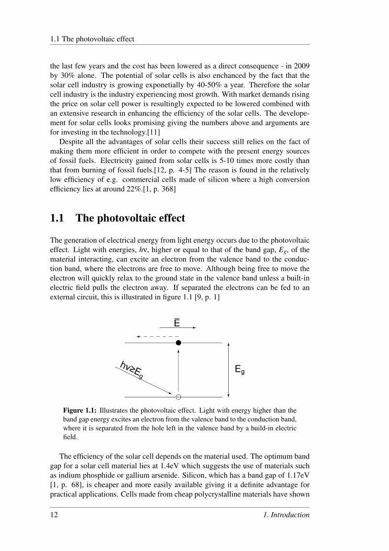
The generation of electrical energy from light energy occurs due to the photovoltaiceffect. Light with energies, hν, higher or equal to that of the band gap, Eg, of thematerial interacting, can excite an electron from the valence band to the conduc-tion band, where the electrons are free to move. Although being free to move theelectron will quickly relax to the ground state in the valence band unless a built-inelectric field pulls the electron away. If separated the electrons can be fed to anexternal circuit, this is illustrated in figure 1.1 [9, p. 1]
Figure 1.1: Illustrates the photovoltaic effect. Light with energy higher than theband gap energy excites an electron from the valence band to the conduction band,where it is separated from the hole left in the valence band by a build-in electricfield.
The efficiency of the solar cell depends on the material used. The optimum bandgap for a solar cell material lies at 1.4eV which suggests the use of materials suchas indium phosphide or gallium arsenide. Silicon, which has a band gap of 1.17eV[1, p. 68], is cheaper and more easily available giving it a definite advantage forpractical applications. Cells made from cheap polycrystalline materials have shown
12 1. Introduction
1.2 Plasmons
yields of 10% efficiency.[1, p. 368]Even though silicon has a band gap of 1.17eV, this is not a direct band gap. In
order for incident photons with energies lower than that of silicon’s direct band gapat 3.45eV [1, p. 68] to contribute to the excitation of electrons, the light must beassisted by lattice vibrations called phonons.
1.2 Plasmons
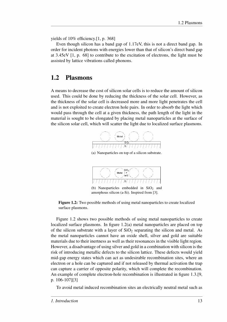
A means to decrease the cost of silicon solar cells is to reduce the amount of siliconused. This could be done by reducing the thickness of the solar cell. However, asthe thickness of the solar cell is decreased more and more light penetrates the celland is not exploited to create electron hole pairs. In order to absorb the light whichwould pass through the cell at a given thickness, the path length of the light in thematerial is sought to be elongated by placing metal nanoparticles at the surface ofthe silicon solar cell, which will scatter the light due to localized surface plasmons.
(a) Nanoparticles on top of a silicon substrate.
(b) Nanoparticles embedded in SiO2 andamorphous silicon (a-Si). Inspired from [3].
Figure 1.2: Two possible methods of using metal nanoparticles to create localizedsurface plasmons.
Figure 1.2 shows two possible methods of using metal nanoparticles to createlocalized surface plasmons. In figure 1.2(a) metal nanoparticles are placed on topof the silicon substrate with a layer of SiO2 separating the silicon and metal. Asthe metal nanoparticles cannot have an oxide shell, silver and gold are suitablematerials due to their inertness as well as their resonances in the visible light region.However, a disadvantage of using silver and gold in a combination with silicon is therisk of introducing metallic defects to the silicon lattice. These defects would yieldmid-gap energy states which can act as undesirable recombination sites, where anelectron or a hole can be captured and if not released by thermal activation the trapcan capture a carrier of opposite polarity, which will complete the recombination.An example of complete electron-hole recombination is illustrated in figure 1.3.[9,p. 106-107][3]
To avoid metal induced recombination sites an electrically neutral metal such as
1. Introduction 13

1.2 Plasmons
Figure 1.3: An example of complete electron-hole recombination. Inspired from[9, p. 112].
tin can be chosen. A disadvantage of using tin is its oxidation when in contact withair. This can be avoided by embedding the tin nanoparticles in a host material suchas SiO2 combined with amorphous silicon. As the Si-O bonding enthalpy is muchlarger than that of Sn-O, the oxidation of tin nanoparticles embedded in SiO2, dueto oxygen inter diffusion, is not likely. This scenario is shown in figure 1.2(b).[3]
14 1. Introduction
Chapter 2
Problem Statement
As mentioned in Chapter 1, solar cells’ competitiveness to other energy sources ishighly dependent on their efficiency. To be able to improve the efficiency of solarcells it is important to understand the influence of certain limiting factors. The fo-cus of this thesis is to fabricate a functional solar cell using phosphorus as dopanton polycrystalline p-type silicon substrates. Furthermore the aim is to investigatethe enhancement of the cell efficiency through various optimizing fabrication tech-niques. Based on this the following initiating problem is the foundation of thethesis:
"How can a basic solar cell with rectifying diode behavior be fabricated, and howcan the specific characteristics of the solar cell be enhanced?"
15

16 2. Problem Statement
Chapter 3
Electrons and Holes in Energy Bands
This chapter deals with the dynamics and kinematics of electrons and holes in en-ergy bands. The similarity of the properties of electrons and holes are investigated.Furthermore the concept of impurities in a semiconductor crystal is described.
3.1 Electron and hole motion in semiconductor bands
Semiconductors differ from metals due to the fact that charge carries can includenot only electrons in the conduction band but also empty electron states or holes inthe valence band. When an external source of applied electrical or magnetic fieldinteracts with the current carriers the behavior is strongly dependent on the energyband structure of the semiconductor and is characterized by their effective mass andcharge.[1, p.74]
The electrons in the semiconductor are described by Bloch states or waves withinthe regime of a periodic potential. The corresponding wave functions to the Blochstates are wave-like and non-localized. To describe electron motion from one pointin the band to another it is represented by a localized wave packet in order to assigna particular coordinate at a particular time. The wave packet, also called envelopefunction, is created by a superposition of linear time-dependent Bloch functions ofvarious wave vectors~k and coefficients an~k with maximum at a particular value~k0:
fn~k0(~r, t) =
∫d3kan~kΨn~k(~r, t). (3.1)
The time dependent Bloch functions are written as
Ψn~k(~r, t) = ei~k·~run~k(~r)e−i(En~k/~)t , (3.2)
which is a product of two plane wave functions, spatial and time dependent, and aperiodic Bloch function un~k(~r). En~k is the energy eigenvalue of the Bloch state.
17
3.1 Electron and hole motion in semiconductor bands
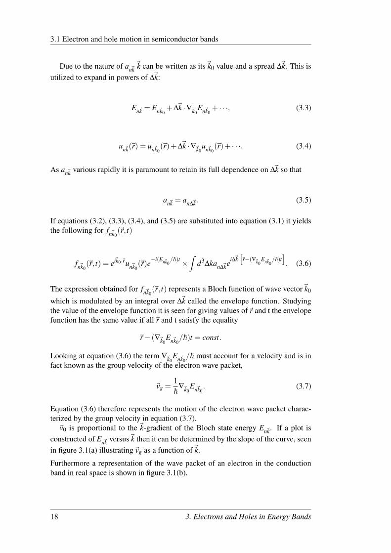
Due to the nature of an~k~k can be written as its~k0 value and a spread ∆~k. This is
utilized to expand in powers of ∆~k:
En~k = En~k0+∆~k ·∇~k0
En~k0+ · · ·, (3.3)
un~k(~r) = un~k0(~r)+∆~k ·∇~k0
un~k0(~r)+ · · ·. (3.4)
As an~k various rapidly it is paramount to retain its full dependence on ∆~k so that
an~k = an∆~k. (3.5)
If equations (3.2), (3.3), (3.4), and (3.5) are substituted into equation (3.1) it yieldsthe following for fn~k0
(~r, t)
fn~k0(~r, t) = ei~k0·~run~k0
(~r)e−i(En~k0
/~)t×∫
d3∆kan∆~ke
i∆~k·[~r−(∇~k0
En~k0/~)t
]. (3.6)
The expression obtained for fn~k0(~r, t) represents a Bloch function of wave vector~k0
which is modulated by an integral over ∆~k called the envelope function. Studyingthe value of the envelope function it is seen for giving values of~r and t the envelopefunction has the same value if all~r and t satisfy the equality
~r− (∇~k0En~k0
/~)t = const.
Looking at equation (3.6) the term ∇~k0En~k0
/~ must account for a velocity and is infact known as the group velocity of the electron wave packet,
~vg =1~
∇~k0En~k0
. (3.7)
Equation (3.6) therefore represents the motion of the electron wave packet charac-terized by the group velocity in equation (3.7).
~v0 is proportional to the ~k-gradient of the Bloch state energy En~k. If a plot isconstructed of En~k versus~k then it can be determined by the slope of the curve, seenin figure 3.1(a) illustrating~vg as a function of~k.
Furthermore a representation of the wave packet of an electron in the conductionband in real space is shown in figure 3.1(b).
18 3. Electrons and Holes in Energy Bands

3.1 Electron and hole motion in semiconductor bands
(a) The energy as a function of the wavevector~k and the groupvelocity as a function of~k.
(b) Representation of a wave packet of the electron in the con-duction band.
Figure 3.1: Inspired from [1, p.75].
3.1.1 Effective mass
The wave packet describing the motion of the electron can be regarded as a semi-classical description and thus several analogies concerning velocity, force and en-ergy can be used from a classical point of view. First the time derivative is taken ofthe group velocity~vg yielding the acceleration:
d~vg
dt=
ddt
(1~
∇~kEn~k
)=
1~
∇~k
dEn~kdt
.
From classical mechanics the time derivative of the energy is related to the forceacting on the particle
dEdt
= ~F ·~vg. (3.8)
3. Electrons and Holes in Energy Bands 19
3.1 Electron and hole motion in semiconductor bands
Equation (3.8) can be rewritten as
d~vg
dt=
1~(∇~k~vg
)·~F . (3.9)
It is assumed that ~F is independent on~k here.On the right hand side of equation (3.9)~vg is replaced by its definition in equation
(3.7) yielding
d~vg
dt=
1~2
(∇k∇kEn~k
)·~F . (3.10)
The left hand side in equation (3.10) contains the acceleration and by comparison toNewton’s second law of motion the quantity ~2∇k∇kEn~k must have the dimension ofinverse mass. Hence, for a simple parabolic band, the inverse effective mass tensoris
1m∗n
=1~2
∂2En~k∂k2 . (3.11)
Conclusively it seen that the curvature of the energy band is proportional to theinverse effective mass. If the curvature is increased the effective mass decreasesaccordingly.
3.1.2 Dynamics of electrons and holes
From equation (3.8) the chain rule is applied to the derivative of E yielding
d~kdt·∇kEn~k =
~F ·~vg.
The gradient of the band energy is replaced with the aid of equation (3.7) and bycancellation of the group velocity on each side the equation becomes
~F = ~d~kdt
. (3.12)
If the expression for the force ~F in equation (3.12) is compared to the classicalrelation
~F =d~pdt
,
the quantity ~~k is identified as ~p, the so-called crystal momentum of the electron inthe crystal lattice.
To describe the dynamics of electrons in the crystal an external force of an ap-plied field ~E is examined. The force becomes
~F =−e~E (3.13)
20 3. Electrons and Holes in Energy Bands

3.1 Electron and hole motion in semiconductor bands
and thus
~d~kdt
=−e~E. (3.14)
By applying an electrical field the wave vector~k changes over time as a direct con-sequence. Combining equation (3.10) and (3.13) yields
d~vg
dt=
1m∗·~F ⇔
d~vg
dt=−e
(1
m∗
)~E,
showing that the electron wave packet is in fact accelerated by the applied electricalfield yielding a current.
The electrical conduction described in the above is only valid for a partially filledenergy band. When an external field is applied an electron of wave vector~k canmake a transition in the band if there is an empty state available of different wavevector nearby. On the other hand if the band is completely filled the electron cannotundergo any transition as there are no available states. Thus the conductivity of afilled band is zero.
A distinction between insulators and conductors can then be stated. The formerhas all bands including a certain band completely filled with electrons at 0K. Allbands above are completely empty and an energy gap separate the two by an amountEg >> kBTr, where Tr is the room temperature. The latter has at least one partiallyfilled band and if the present electrons excite due to thermal excitation across a nor-mally forbidden energy gap from a filled band, it is defined to be a semiconductor.If one or more bands continue to be partially filled at 0K the material is a metal orsemi metal. [1, p. 74-77]
3.1.3 Holes
When an electron is excited from a filled energy band to an unfilled energy bandthe empty state left is called a hole state. The holes lying near the band edge of thevalence band are of great importance in the semiconductor as they contribute to thecurrent. To study the properties of a hole its wave vector is examined firstly.
The total wave vector of the electrons in the filled band is zero, ∑~k = 0, summingover all states in the Brillouin zone. If the band is filled all pairs of~k and -~k are filledresulting in a total wave vector of zero. In the case of a missing electron of wavevector~ke the total wavevector of the system is changed to -~ke obtained by the hole.The hole wave vector is not that of the missing electron but the negative of it.
The energy of the hole is deduced in the following. The excited electron expe-riences an increase in
∣∣∣~ke
∣∣∣ resulting in a decrease of the vacant state energy by the
amount Ee(~ke). The vacant state moves lower into the valence band, from a higherenergy state to a lower energy state. However, the total energy of the electronsin the band increases by an equal amount as an occupied state makes the reversetransition. Conclusively the energy of the hole, Eh(~kh), is defined to
Eh(~kh) =−Ee(~ke).
3. Electrons and Holes in Energy Bands 21

3.1 Electron and hole motion in semiconductor bands
Furthermore due to~kh =−~ke it follows that,
Eh(~kh) =−Ee(−~kh).
As stated in the above it follows that for every state~k there is another state of equalenergy with wave vector -~k 1, thus
Eh(~kh) =−Ee(~kh). (3.15)
It is seen that Ee is a decreasing function of its argument and Eh is an increasingfunction of its argument.
If it is assumed that the valence band is spherical parabolic the energy dispersionis
Ee(~ke) = EV +~2k2
e2m∗e
, (3.16)
where EV is the energy of the valence band edge and m∗e is the negative effectivemass. The hole energy is thus
Eh(~kh) =−EV −~2k2
h2m∗e
.
The result is rewritten as
Eh(~kh) =−EV +~2k2
h2m∗h
, (3.17)
where m∗h is the mass of the hole. It follows from equation (3.11) that the effec-tive mass is inversely proportional to the curvature of the energy band. Since thedispersion for the electron follows the relation in equation (3.16), and according toequation (3.17), it is clear that m∗h = −m∗e . Since m∗e is negative, m∗h is positive[1,p. 77-78]. The dispersion for the missing electron and hole energies versus wavevector are shown in figure 3.2.
Lastly the group velocity and the charge of the hole are studied. The group velocityis given by
~vgh =1~
∇~khEh(~kh),
and for the electron missing in the valence band
~vge =1~
∇~keEe(~ke).
With~ke =−~kh it becomes
~vge =−1~
∇~khEe( ~−kh) =−
1~
∇~khEe(~kh).
1This has its origins in the fact that the bands are always symmetric under the inversion of~k→−~k.[6, p.195]
22 3. Electrons and Holes in Energy Bands

3.2 Semiconductor impurities
(a) Missing electron band
(b) Hole band
Figure 3.2: (a) The hole energy Eh versus wave vector and (b) missing electronenergy Ee versus wave vector. The circles represensate a pair of missing electronand hole. Inspired from [1, p.78].
Using equation (3.15) yields
~vge =1~
∇~khEh(~kh) =~vgh.
Conclusively the group velocity of the hole and the missing electron are identical.Finally the charge of the hole can be found buy utilizing the equation of motion,
(3.14), to the missing electron
~d~ke
dt=−e~E.
Using~ke = ~−kh the equation of motion for the hole is
~d~kh
dt= eh~E,
It is seen that the charge of the hole is positive, eh =+e.
3.2 Semiconductor impurities
Silicon doped with phosphorus introduces impurities in the structure of the semi-conductor and this has several effects. Silicon is a group IV element that enables
3. Electrons and Holes in Energy Bands 23
3.2 Semiconductor impurities
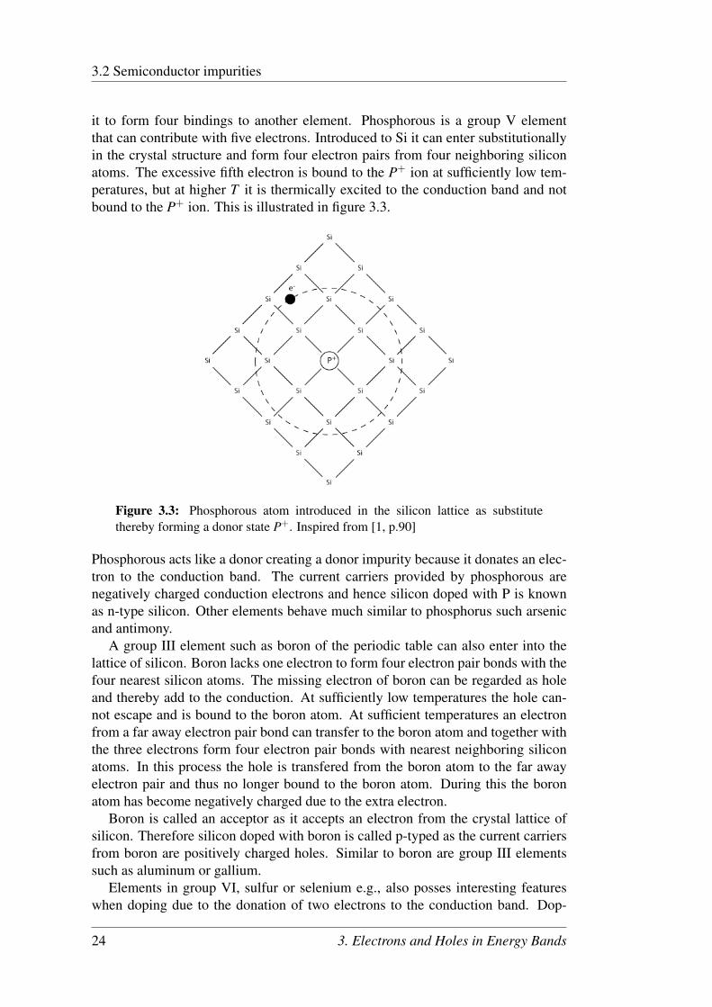
it to form four bindings to another element. Phosphorous is a group V elementthat can contribute with five electrons. Introduced to Si it can enter substitutionallyin the crystal structure and form four electron pairs from four neighboring siliconatoms. The excessive fifth electron is bound to the P+ ion at sufficiently low tem-peratures, but at higher T it is thermically excited to the conduction band and notbound to the P+ ion. This is illustrated in figure 3.3.
Figure 3.3: Phosphorous atom introduced in the silicon lattice as substitutethereby forming a donor state P+. Inspired from [1, p.90]
Phosphorous acts like a donor creating a donor impurity because it donates an elec-tron to the conduction band. The current carriers provided by phosphorous arenegatively charged conduction electrons and hence silicon doped with P is knownas n-type silicon. Other elements behave much similar to phosphorus such arsenicand antimony.
A group III element such as boron of the periodic table can also enter into thelattice of silicon. Boron lacks one electron to form four electron pair bonds with thefour nearest silicon atoms. The missing electron of boron can be regarded as holeand thereby add to the conduction. At sufficiently low temperatures the hole can-not escape and is bound to the boron atom. At sufficient temperatures an electronfrom a far away electron pair bond can transfer to the boron atom and together withthe three electrons form four electron pair bonds with nearest neighboring siliconatoms. In this process the hole is transfered from the boron atom to the far awayelectron pair and thus no longer bound to the boron atom. During this the boronatom has become negatively charged due to the extra electron.
Boron is called an acceptor as it accepts an electron from the crystal lattice ofsilicon. Therefore silicon doped with boron is called p-typed as the current carriersfrom boron are positively charged holes. Similar to boron are group III elementssuch as aluminum or gallium.
Elements in group VI, sulfur or selenium e.g., also posses interesting featureswhen doping due to the donation of two electrons to the conduction band. Dop-
24 3. Electrons and Holes in Energy Bands

3.2 Semiconductor impurities
ing with a group II element would as a result lead to a double acceptor state.[1, p.89-90]
3. Electrons and Holes in Energy Bands 25

3.2 Semiconductor impurities
26 3. Electrons and Holes in Energy Bands
Chapter 4
Diffusion
This chapter aims to describe the physics of diffusing impurities into a oppositedoped substrate and the methods utilized to measure the dopant concentration achieved.
4.1 Fick’s diffusion equation
A material which is free to move and introduced to a dopant will experience a netredistribution of the impurity atoms away from the concentration maximum. Thismovement away from the concentration maximum will cause the gradient of theconcentration to decrease. This is one of the basic laws of diffusion. Illustratedlater in 4.1(a).
In one dimension Fick’s first law takes the form
J =−D∂C(x, t)
∂x, (4.1)
where J is the flux of material, D is the coefficient of diffusion, and C is the impurityconcentration. The negative sign is due to the before mentioned fact, that there isnet movement away from the concentration maximum.
As the diffusing material is usually not easily measured, Fick’s second law hasbeen developed involving more easily measured quantities. If a differential vol-ume element of length dx in a long bar of material with a uniform cross section isconsidered, then
J2− J1
dx=
∂J∂x
,
where J1 and J2 is the flux entering and leaving the volume, respectively. If thesetwo fluxes are not equal the concentration of the diffusing species has changed. Thecontinuity equation is then
27
4.1 Fick’s diffusion equation
dNdt
= Adx∂C∂t
=−A(J2− J−1) =−Adx∂J∂x
, (4.2)
where N is the number of impurities in the volume element and A is the cross-sectional area. Equation (4.2) can be reduced to
∂C(x, t)∂t
=−∂J∂x
. (4.3)
If equation (4.3) is inserted in equation (4.1) one has
∂C(x, t)∂t
=∂
∂x
(D
∂C∂x
), (4.4)
which is the most general form of Fick’s second law. If it is assumed that thediffusion coefficient is independent of position equation (4.4) reduces to
∂C(z, t)∂t
= D∂2C(z, t)
∂z2 ,
where z is the direction into the wafer. Fick’s second law in three dimensions for anisotropic medium is then
∂C∂t
= D∇2C. (4.5)
Equation (4.5) is a differential equation, which is first order in time and second or-der in position. To solve this differential equation at least two independent boundaryconditions are required. The diffusion coefficient in equation (4.5) can be found bymeans of atomistic models, but for now the diffusion coefficient will be assumed tobe constant. [2, p. 43-45]
The concentration is found for the predeposition- and drive-in diffusion situa-tions. The predeposition diffusion situation requires a constant surface concentra-tion. Thus the boundary conditions are
C(z,0) = 0C(∞, t) = 0C(0, t) =Cs,
which yields the solution
28 4. Diffusion
4.1 Fick’s diffusion equation
C(z, t) =Cs erfc(
z2√
Dt
), t > 0. (4.6)
In equation (4.6) Cs is the fixed surface concentration, erfc is the complementaryerror function and
√Dt is the characteristic diffusion length.
The dose diffused into the substrate varies with the time of diffusion and can bederived by integrating the profile of the concentration
QT (t) =∫
∞
0C(z, t)dz
=2√π
Cs√
Dt.
The dose increase as the square root of the time and is measured in units of impuri-ties per unit area.
For the drive-in diffusion situation the source of diffusing impurity atoms is lim-ited to QT . For a diffusion length much larger that the width of the initial profile,the initial profile can be approximated to be a delta function, meaning that the initialimpurity atoms are only present at the surface. This gives the boundary conditions
C(z,0) = 0, z 6= 0C(∞, t) = 0
dC(0, t)dz
= 0
QT (t) =∫
∞
0C(z, t)dz = constant.
The solution for these boundary conditions is a Gaussian with center at z = 0
C(z, t) =QT√πDt
e−z2
4Dt , t > 0. (4.7)
As the source of diffusing impurity atoms is limited the surface concentration de-creases with time as
Cs =C(0, t) =QT√πDt
.
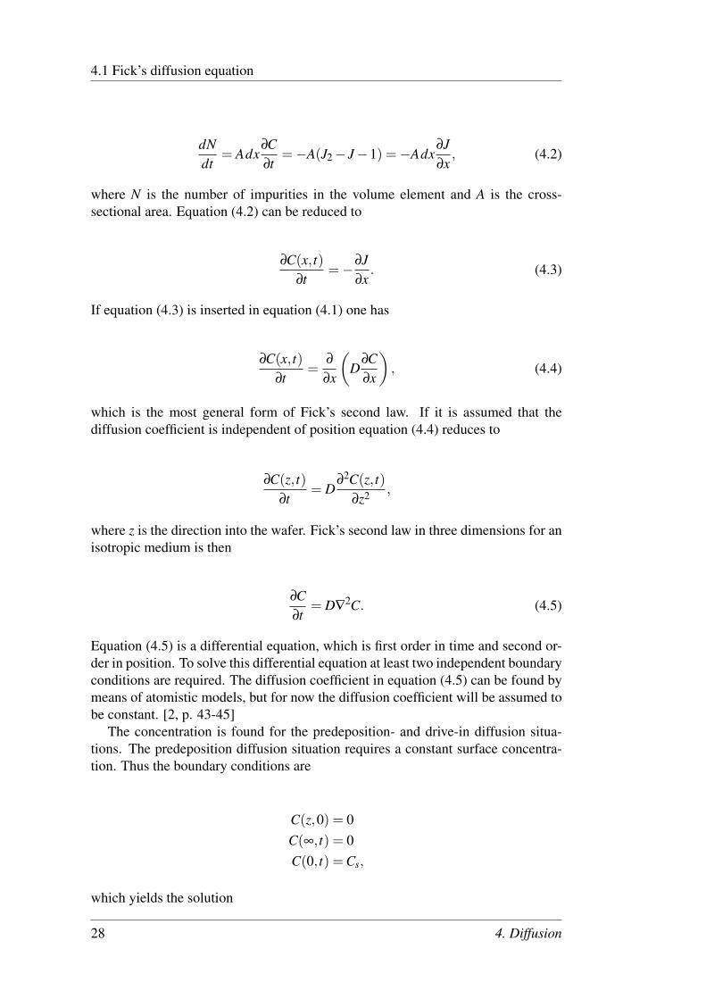
Figure 4.1(a) and 4.1(b) illustrates the predeposition and drive-in diffusion, respec-tively.
4. Diffusion 29
4.1 Fick’s diffusion equation
(a) Predeposition diffusion.
(b) Drive-in diffusion
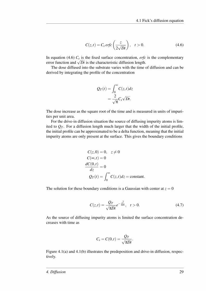
Figure 4.1: Illustrates the concentration profiles for predeposition- and drive-indiffusion for three different characteristic diffusion lengths.
Assuming that phosphorus is diffusing into a silicon substrate with a uniform con-centration of boron, CB, and that Cs >> CB, a pn-junction will form at a cer-tain depth, where the concentration of phosphorus cancels out the concentration ofboron, as boron and phosphorus in silicon are p- and n-type dopants, respectively.From equation (4.7) the junction depth x j can be shown to be
x j =
√4Dt ln
[QT
CB√
πDt
]
30 4. Diffusion
4.2 Profile analysis
in case of drive-in diffusion. And from equation (4.6) in case of predepositiondiffusion to be
x j = 2√
Dterfc−1[
CB
Cs
],
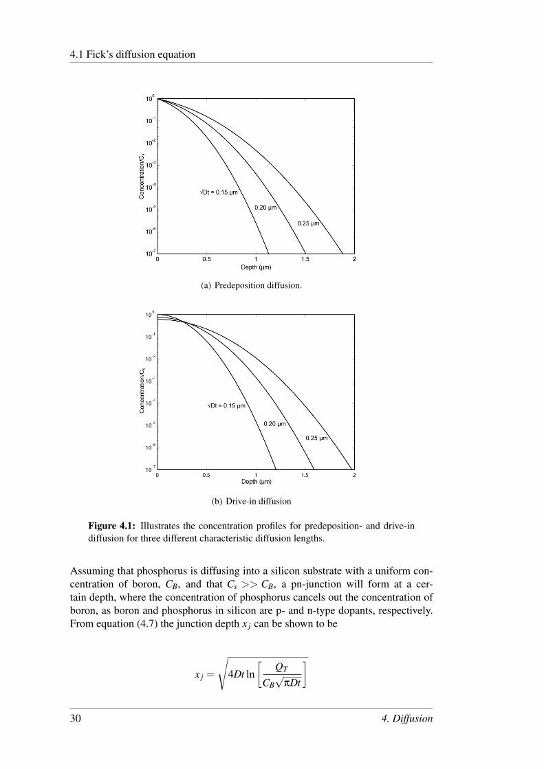
see figure 4.2.
Figure 4.2: Illustrates a typical concentration plot of impurities as a function ofdepth. At the junction depth the bulk impurities succeed the diffused impurities.
4.2 Profile analysis
When the impurity ions have been diffused, it is desirable to obtain the concentra-tion of the impurities as a function of depth. This can be done by measuring thesheet resistance
RS = [q∫
µ(C)Ce(z)dz]−1, RS =
[Ω
square
]where Ce(z) is the carrier concentration, µ(C) the concentration dependent mobility,and q is the charge.
The sheet resistance can be measured in several ways, where the simplest is byusing a four-point probe. Four-point probe measurements can be conducted in sev-eral ways itself. The most common is the collinear approach, see figure 4.3(a),where current is passed through the sample between two outer probes and the volt-age is measured between the inner pair of probes. The sheet resistance is found by
4. Diffusion 31

4.2 Profile analysis
the ratio between the measured voltage drop and the forced current. The result mustbe multiplied by a correction factor, which depends on the probe geometry and theratio between the probe spacing and the thickness of the diffusion. However, forprobe spacings much larger that the junction depth, the correction factor is 4.5325in the collinear approach. For this method to be reliable the underlying substratemust be of much higher resistance than the layer to be measured or the layer to bemeasured must form a reverse-biased diode with the substrate. In the latter case, theforce of the probe to the surface should not be too large or the probes could pene-trate very shallow junctions and the sheet resistance measurements would includethe effect of the depleted region near the junction.
(a) Collinear approach. (b) Van der Pauw approach.
Figure 4.3: Illustrates two methods of measuring the sheet resistance of a sample.Inspired from [2, p. 57].
Another approach to the four-point probe measurement is the Van der Pauwmethod, see figure 4.3(b), which is done by contacting the edge of a randomlyshaped sample at four places. A current is again forced between two contacts andthe voltage is measured between two other contacts. To obtain the best accuracypossible the sample is rotated 90 three times so that four different measurementsare conducted. The average resistance is then
R =14
[V12
I34+
V23
I41+
V34
I12+
V41
I23
].
And the sheet resistance is
RS =π
ln(2)F(Q)R,
32 4. Diffusion
4.2 Profile analysis
where F(Q) is the geometry dependent correction factor. For a square the contactsmust be made on the side of the sample, which yields a correction factor F(Q) = 1.For proper measurements ohmic contacts can be applied. [2, p. 55-56]
4. Diffusion 33

4.2 Profile analysis
34 4. Diffusion

Chapter 5
Semiconductor Statistics
This chapter contributes to the calculation of the concentration of electrons andholes in the spherical parabolic and ellipsoidal energy bands in semiconductingmaterials. Furthermore the Fermi energy is found for an intrinsic semiconductorand the electron-hole ratio is derived for extrinsic semiconductors.
In order to calculate certain properties such as the diffusion potential it is neces-sary to know the concentrations of negatively and positively charged carriers in theconduction band and the valence band, respectively. Firstly, carriers can arise dueto different types of excitations like thermal and optical excitations from valence toconduction band. If excitations mostly occur from valence band to conduction bandthe semiconductor is classified as an intrinsic semiconductor. Secondly, current car-riers can occur by excitations from or to impurity states. If excitations mostly occurfrom impurity states the semiconductor is classified as an extrinsic semiconductor.And thirdly, current carriers can occur by excitations from an external source. Inthis chapter thermal excitations will be ignored meaning the semiconductor is inthermal equilibrium. [1, p.101]
5.1 Intrinsic semiconductors
If an intrinsic semiconductor with band gap Eg is considered, the Fermi-Dirac dis-tribution
fFD(~k) =1
eE~k−EF
kBT +1, (5.1)
specifies the electron occupation number of a state of energy E~k in thermal equilib-rium at temperature T . kB is Boltzmann’s constant and EF is the Fermi energy. IfT = 0 then fFD = 1 when E~k < EF , and fFD = 0 when E~k > EF , signifying that allstates with energies lower than the Fermi energy are occupied and all states withenergies higher than the Fermi energy are unoccupied at T = 0. As the temperaturerises more states with energies lower than the Fermi energy will be unoccupied and
35

5.1 Intrinsic semiconductors
Figure 5.1: The Fermi-Dirac distribution function plotted against the energy forT = 0 and for T 6= 0. Inspired from [1, p. 102]
more states with energies higher than the Fermi energy will be occupied. The twosituations for T = 0 and T > 0 are illustrated in figure 5.1, where the Fermi-Diracdistribution function is plotted against the energy.
The concentration of electrons in the conduction band is given by
n =2Ω
∑~k
fFD(~k)
=2Ω
∑~k
1
eE
c~k−EF
kBT +1, (5.2)
where the sum is over all states in the conduction band with energies Ec~k, Ω is thevolume of the system and the factor 2 is due to spin degeneracy. By converting thesum over~k to an integral
∑~k
−→ Ω
(2π)3
∫d3k,
equation (5.2) becomes
n =2
(2π)3
∫d3k
1
eE
c~k−EF
kBT +1. (5.3)
An analytic evaluation of the Fermi-Dirac integral is only possible with certain ap-proximations of the energy bands. [1, p. 101-103]
5.1.1 Spherical parabolic energy bands
In the case of a spherical parabolic conduction band with an effective mass m∗c , theenergy of the conduction band is given by
Ec~k = EC +~2k2
2m∗c.
36 5. Semiconductor Statistics

5.1 Intrinsic semiconductors
Here EC is the edge of the conduction band. If it is assumed that kBT << EC−EF ,then the quantity +1 in equation (5.1) can be ignored. The Fermi-Dirac distributioncan then be approximated to
fFD(~k)≈ eEF−E
c~kkBT .
Consequently equation (5.3) becomes
n =2
(2π)3
∫e
EF−EC−~2k22m∗c
kBT d3k.
By introducing spherical coordinates
n =2
(2π)3
∫π
0
∫ 2π
0
∫∞
0e
EF−EC−~2k22m∗c
kBT k2 sinϕdkdθdϕ
n =2
(2π)3 2 ·2π
∫∞
0k2e
EF−EC−~2k22m∗c
kBT dk
n =2
2π2 eEF−EC
kBT
∫∞
0k2e−
~2k22m∗ckBT dk,
and changing the variable of integration from k to E = ~2k2
2m∗cthe concentration of
electrons in the conduction band is now
n =2
2π2 eEF−EC
kBT
∫∞
0
12
(2m∗c~2
)3/2
E1/2e−E
kBT dE
n = eEF−EC
kBT
∫∞
0Nc(E)e
− EkBT dE, (5.4)
where
Nc(E) =1
2π2
(2m∗c~2
)3/2
E1/2
is the density-of-states in energy for the conduction band. The density-of-states isplotted against the energy in figure 5.2 and the free carrier concentration is plottedagainst the energy in figure 5.3.
If the constants of integration are left out the integral in equation (5.4) becomes∫∞
0E1/2e−
EkBT dE = Γ
(32
)(kBT )3/2
=
√π
2(kBT )3/2,
reducing equation (5.4) to
n = NceEF−EC
kBT , (5.5)
5. Semiconductor Statistics 37

5.1 Intrinsic semiconductors
Figure 5.2: Density-of-states plotted against the energy. Inspired from [1, p. 104]
Figure 5.3: Free carrier concentration plotted against the energy. Inspired from[1, p. 104]
38 5. Semiconductor Statistics
5.1 Intrinsic semiconductors
where
Nc = 2(
m∗ckBT2π~2
)3/2
(5.6)
is the effective density-of-states for the conduction band. Nc represents a weightedsum of all the occupied states in the conduction band, where the weighting coeffi-cient is the Boltzmann factor. It implies that the higher the energy of the state inthe conduction band, the lower the probability of electron occupation. At a giventemperature Nc represents the degeneracy of the conduction band if it is regarded asa single level with the energy EC. Equation (5.6) is only valid if kBT << EC−EFmeaning that the system is non-degenerate, where the Boltzmann distribution hasbeen used due to approximations. If kBT << EC−EF is not fulfilled the full Fermi-Dirac distribution must be used and consequently the carriers form a degeneratesystem. Whereas non-degenerate semiconductors have relatively low concentrationof shallow impurities, the concentration of shallow impurities is relatively high indegenerate semiconductors. This high concentration of shallow impurities can leadto formation of impurity bands due to overlapping of atomic orbitals of neighbour-ing impurities. The Fermi energy can then lie sufficiently close to the energy of theconduction band resulting in a degenerate behaviour persisting to low temperatures.
Holes in the valence band are states lacking an electron, thus the distributionfunction for holes in the valence band is 1− fFD. The concentration of holes p canthen be written as
p =2Ω
∑~k
[1− fFD(~k)] =2Ω
∑~k
1
eEF−E
v~kkBT +1
,
where Ev~k is the energy of a state in the valence band. As in the situation concerningelectrons the valence band is considered spherical and parabolic with band edge EVand effective mass m∗v . The energy of the valence band state is then
Ev~k = EV −~2k2
2m∗v.
Again the temperature is considered sufficiently low so kBT << EF −EV yieldingthe concentration of holes
p = NveEV−EF
kBT , (5.7)
where Nv is the effective density-of-states for holes
Nv = 2(
m∗vkBT2π~2
)3/2
,
analogous to the electron situation.Combining equation (5.5) and (5.7) the Fermi energy, which is yet unknown, is
eliminated
np = NcNve−Eg
kBT = n2i , (5.8)
5. Semiconductor Statistics 39
5.2 Extrinsic semiconductors
where Eg = EC−EV and ni is the intrinsic carrier concentration. Equation (5.8) iscalled the law of mass action and implies that at a given temperature the productof electron and hole concentrations in a non-degenerate semiconductor is constant.The fundamental approximation is that the difference between the conduction bandand the Fermi energy and between the Fermi energy and the valence band is largecompared to the thermal energy kBT . No assumptions concerning the source of theelectrons and holes have been made. In case of excitation across the band gap inan intrinsic semiconductor n = p due to charge conservation. Thus from equation(5.8) it follows that
n = p = ni = (NcNv)1/2e−
Eg2kBT
= 2(
kBT2π~2
)3/2
(m∗cm∗v)3/4 e−
Eg2kBT . (5.9)
It is seen that the concentration of electrons and holes increases as the temperaturerises and the energy gap is reduced.
As the concentration of n and p has been found the Fermi energy for an intrinsicsemiconductor can be derived from equations (5.5) and (5.9)
2(
m∗ckBT2π~2
)3/2
eEFi−EC
kBT = 2(
kBT2π~2
)3/2
(m∗cm∗v)3/4 e−
Eg2kBT
m∗3/2c e
EFi−ECkBT = (m∗cm∗v)
3/4 e−Eg
2kBT
eEFi−EC+1/2Eg
kBT =
(m∗vm∗c
)3/4
EFi = EC−12
Eg +34
kBT ln(
m∗vm∗c
). (5.10)
From equation (5.10) is seen that when T = 0 the intrinsic Fermi energy lies in themiddle of the band gap. As the temperature rises the Fermi energy will increasewhen m∗v > m∗c and decrease when m∗v < m∗c . If m∗v = m∗c the Fermi energy lies inthe middle of the band gap at all temperatures.[1, p. 103-106]
5.2 Extrinsic semiconductors
When impurity atoms are introduced to an intrinsic semiconductor, the semiconduc-tor becomes extrinsic. The impurity atom, replacing a host atom in the crystal lat-tice, has either a higher or lower valence number than the host atom. If the valencenumber is higher than the one of the replaced host atom, then, at low temperatures,an electron will be bound to the positively charged ion and be excited to the conduc-tion band at higher temperatures. Thus the impurity atom has donated an electronto the conduction band of the semiconductor and consequently the semiconductoris an n-type. If the valence number is lower than the one of the replaced host atom,then the missing electron can be regarded as a hole. At sufficiently low temperatures
40 5. Semiconductor Statistics
5.2 Extrinsic semiconductors
the hole will be bound to the impurity atom, but at rising temperatures the hole willbe replaced by an electron from a lattice atom far away. Thus the impurity atom isnow a negatively charged ion and a hole has been added to the valence band makingthe semiconductor a p-type.[1, p. 90]
Rewriting equations (5.5) and (5.7) to
n = NceEF+EFi−EFi−EC
kBT = nieEF−EFi
kBT
p = NveEV +EFi−EFi−EF
kBT = nieEFi−EF
kBT ,
a general expression for the ratio between the electron and hole concentration canbe derived
np= e2 EF−EFi
kBT . (5.12)
From equation (5.12) it can be concluded that if the Fermi energy of the doped semi-conductor is higher than that of the intrinsic semiconductor, then the concentrationof electrons will be higher than the concentration of holes and vice versa.
The fact that impurity levels are localized states complicates a detailed statisticalanalysis. If a charge carrier of a given spin is already in a localized impurity orbital,it will cause a large change in energy to add a second carrier of opposite spin to theorbital as a result of the Coulomb repulsion of the two carriers. [1, p. 109-110]
5. Semiconductor Statistics 41

5.2 Extrinsic semiconductors
42 5. Semiconductor Statistics
Chapter 6
Junctions in Semiconductors atThermal Equilibrium
This chapter contributes to describing the development of a diffusion potential,build-in electric field, and thus the behaviour of the energy bands in a pn-junction inthermal equilibrium. Furthermore the general principles governing the electronicstructure of a metal-semiconductor junction is described.
To understand the principles of a solar cell it is important to understand the physicstaking place in the junction between n- and p-type materials. The principle im-purities of an n-type material are donors and thus the majority charge carriers areelectrons in the conduction band, arising primarily from the ionized donor atom.Similarly, the principle impurities of a p-type material are acceptors and the ma-jority carriers are holes arising from the acceptor atom. Together with the majoritycharge carriers from the impurity atoms thermally excited electrons and holes arestill present. In case of a p-type material thermally excited electrons in the conduc-tion band are minority carriers and in case of an n-type material thermally excitedholes in the valence band are minority carriers.
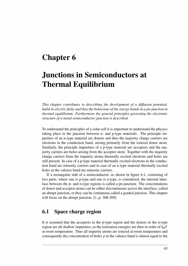
If a rectangular slab of a semiconductor, as shown in figure 6.1, consisting oftwo parts, where one is p-type and one is n-type, is considered, the internal inter-face between the p- and n-type regions is called a pn-junction. The concentrationsof donor and acceptor atoms can be either discontinuous across the interface, calledan abrupt junction, or they can be continuous called a graded junction. This chapterwill focus on the abrupt junction. [1, p. 308-309]
6.1 Space charge region
It is assumed that the acceptors in the p-type region and the donors in the n-typeregion are all shallow impurities, as the ionization energies are then in order of kBTat room temperature. Thus all impurity atoms are ionized at room temperature andconsequently the concentration of holes p in the valence band is almost equal to the
43
6.1 Space charge region
Figure 6.1: Illustration of a rectangular slab of a semiconductor consisting of p-type material to the left and n-type material to the right. The interface between thep- and n-type region is called a pn-junction. Inspired from [1, p. 309].
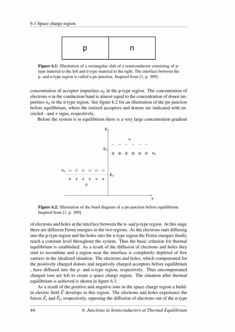
concentration of acceptor impurities na in the p-type region. The concentration ofelectrons n in the conduction band is almost equal to the concentration of donor im-purities nd in the n-type region. See figure 6.2 for an illustration of the pn-junctionbefore equilibrium, where the ionized acceptors and donors are indicated with en-circled - and + signs, respectively.
Before the system is in equilibrium there is a very large concentration gradient
Figure 6.2: Illustration of the band diagram of a pn-junction before equilibrium.Inspired from [1, p. 309].
of electrons and holes at the interface between the n- and p-type region. At this stagethere are different Fermi energies in the two regions. As the electrons start diffusinginto the p-type region and the holes into the n-type region the Fermi energies finallyreach a constant level throughout the system. Thus the basic criterion for thermalequilibrium is established. As a result of the diffusion of electrons and holes theystart to recombine and a region near the interface is completely depleted of freecarriers in the idealized situation. The electrons and holes, which compensated forthe positively charged donors and negatively charged acceptors before equilibrium, have diffused into the p- and n-type region, respectively. Thus uncompensatedcharged ions are left to create a space charge region. The situation after thermalequilibrium is achieved is shown in figure 6.3.
As a result of the positive and negative ions in the space charge region a build-in electric field ~E develops in this region. The electrons and holes experience theforces ~Fe and ~Fh, respectively, opposing the diffusion of electrons out of the n-type
44 6. Junctions in Semiconductors at Thermal Equilibrium

6.2 Charge density variation
Figure 6.3: Illustration of the band diagram of a pn-junction after equilibrium.Inspired from [1, p. 310]
region and holes out of the p-type region due to the build-in electric field. Equilib-rium requires that the current densities equals zero:
~Je = enµe~E + eDe∇n = 0~Jh = enµh~E + eDh∇p = 0,
where ~Je and ~Jh are current densities for electrons and holes, µe and µh are theirmobilities, and De and Dh their diffusion coefficients.[1, p. 308-310]
6.2 Charge density variation
The charge density ρ(x) at a point x is given by
ρ(x) = e[nd(x)−na(x)+ p(x)−n(x)].
For x ≥ xn the charge density is zero, as the thermally excited electrons and holescompensate for each others’ charge. The charge due to the donor contribution toconduction electrons compensate for the positively charged donor ions. A Simi-lar argument can be used to state that the charge density is zero for x ≤ xp. For0 ≤ x ≤ xn on the n-type side of the space charge region the only contribution tothe charge density is the concentration of donor ions nd , as the region is depletedof free charge carriers and no acceptor ions are present in the region. Finally for0 ≥ x ≥ xp on the p-type side of the space charge region the only contribution tothe charge density is the concentration of acceptor ions na. As this region is alsodepleted of free charge carriers and no donor ions are present. Conclusively thecharge density can be expressed as
ρ(x) = 0 for x≤ xp and xn ≤ xρ(x) =−ena for xp ≤ x≤ 0 (6.2a)ρ(x) = end for 0≤ x≤ xn. (6.2b)
A plot of the charge density against x for an abrupt pn-junction is shown in figure6.4.
6. Junctions in Semiconductors at Thermal Equilibrium 45

6.3 Diffusion potential
Figure 6.4: Illustration of the charge density ρ across the pn-junction. Inspiredfrom [1, p. 311]
6.3 Diffusion potential
A build-in electric field arises in the space charge region due to the particular chargedensity distribution and can be written as the negative gradient of the electrostaticpotential V (~r)
~E =−∆V (~r). (6.3)
The potentials in the different regions of the pn-junction are illustrated in figure 6.5.
Figure 6.5: Illustrates the potential across the pn-junction. Vd is the diffusionpotential, which is the difference between the potentials Vn and Vp. Inspired from[1, p. 311].
The diffusion potential Vd is the difference between the potentials in the neutraln-type and the p-type regions.
Vd =Vn−Vp. (6.4)
In the situation of an ideal abrupt junction, where the build-in electric field is limitedto the space charge region, the diffusion potential can be derived using the fact that
46 6. Junctions in Semiconductors at Thermal Equilibrium

6.4 Build-in electric field
the system is at equilibrium. From equation (5.5) the electron concentration in theneutral n-type region can be written as
nn = NceEF−ECn
kBT (6.5)
and in the neutral p-type region as
np = NceEF−ECp
kBT , (6.6)
where ECn and ECp are the energies of the conduction band minima in the neutraln- and p-type region, respectively. By isolating EF and then equalizing equation(6.5) and (6.6) the difference in conduction band minima between the neutral n-and p-type region is found to
ECp−ECn = kBT ln(
nn
np
)= kBT ln
(ndna
n2i
),
where nn = nd and the law of mass action
np =n2
ipp
=n2
ina
,
from equation (5.8) have been utilized. Generally, the conduction band minimumrelates to the potential via
EC =−eV,
e being the elementary charge. From equation (6.4) the diffusion potential is givenas
Vd =1e
(ECp−ECn
)=
kBTe
ln(
nn
np
).
6.4 Build-in electric field
To find the build-in electric field inside the space charge region it is seen fromequation (6.3) that the potential in this region needs to be known. This can bederived by solving Poisson’s equation with the charge density given by equation(6.2a) and (6.2b)
d2Vdx2 =−ρ(x)
ε0ε, (6.7)
6. Junctions in Semiconductors at Thermal Equilibrium 47

6.4 Build-in electric field
where ε is the dielectric constant of the junction.If the region xp ≤ x≤ 0 is regarded, Poisson’s equation becomes
d2Vdx2 =−d~E
dx=
ena
ε0ε,
and after integration
dVdx
=−~E(x) = enaxε0ε
+ c1. (6.8)
The constant of integration c1 is derived utilizing the boundary condition ~E(xp) = 0:
c1 =−enaxp
ε0ε
and equation (6.8) yields the build-in electric field at the p-type side of the spacecharge region
~E(x) =−ena
ε0ε(x− xp). (6.9)
Similarly the build-in electric field on the n-type side of the space charge region,where 0≤ x≤ xn, can be found
~E(x) =end
ε0ε(x− xn). (6.10)
Overall charge neutrality, illustrated in figure 6.6, in the space charge region requiresthat
xpna =−xnnd,
Figure 6.6: Illustrates the overall charge neutrality in the space charge region.Inspired from [1, p. 313].
which requires that ~E(x) is continuous at x = 0
~E(0) =enaxp
ε0ε=−endxn
ε0ε.
At x = 0 the maximum electric field ~Em of the space charge region is found. This isillustrated in figure 6.7.
48 6. Junctions in Semiconductors at Thermal Equilibrium

6.5 Energy bands in space charge region
Figure 6.7: A plot of the build-in electric field as a function of x. Inspired from[1, p. 314].
6.5 Energy bands in space charge region
To find the potential energy of an electron in the pn-junction the potential V (x) ismultiplied by −e. If the valence band edge EV is taken to be zero in the neutralp-type region, then it has the value
EV (x) =−eV (x) (6.11)
in the space charge region. As the band gap Eg = EC−EV is constant in real space,an expression for the conduction band edge energy can be found
EC(x) = Eg− eV (x). (6.12)
The potential can be derived through
dVdx
=−~E(x).
This is done using the expressions (6.9) and (6.10) for the build-in electric fieldin the p- and n-type side of the space charge region, respectively. If the boundarycondition V (xp) = Vp is used the potential in the p-type side of the space chargeregion is
V (x) =ena(x− xp)
2
2ε0ε+Vp, (6.13)
and if the boundary condition V (xn) = Vn is used in the n-type side of the spacecharge region, the potential is
V (x) =end(x− xn)
2
2ε0ε+Vn. (6.14)
Thus, if equation (6.13) and (6.14) are substituted into equation (6.11) and (6.12),respectively, then the behaviour of the valence and conduction band edge in thespace charge region is found. The behaviour of the bands are presented in figure6.8. The band edges are tilted in the space charge region and the Fermi energy isconstant throughout the structure due to thermal equilibrium. Considering the quasi-Fermi energies EFn and EF p in the neutral n- and p-type regions before equilibrium,where EFn < EF p, then the Fermi energy is given by
EF = EFn− eVd = EF p. (6.15)
6. Junctions in Semiconductors at Thermal Equilibrium 49
6.6 Solar cells
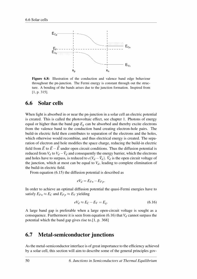
Figure 6.8: Illustration of the conduction and valence band edge behaviourthroughout the pn-junction. The Fermi energy is constant through out the struc-ture. A bending of the bands arises due to the junction formation. Inspired from[1, p. 315].
6.6 Solar cells
When light is absorbed in or near the pn-junction in a solar cell an electric potentialis created. This is called the photovoltaic effect, see chapter 1. Photons of energyequal or higher than the band gap Eg can be absorbed and thereby excite electronsfrom the valence band to the conduction band creating electron-hole pairs. Thebuild-in electric field then contributes to separation of the electrons and the holes,which otherwise would recombine, and thus electrical energy is created. The sepa-ration of electron and hole modifies the space charge, reducing the build-in electricfield from ~E to ~E− ~E under open circuit conditions. Thus the diffusion potential isreduced from Vd to Vd−Vd and consequently the energy barrier, which the electronsand holes have to surpass, is reduced to e(Vd−Vd). Vd is the open circuit voltage ofthe junction, which at most can be equal to Vd , leading to complete elimination ofthe build-in electric field.
From equation (6.15) the diffusion potential is described as
eVd = EFn−EF p.
In order to achieve an optimal diffusion potential the quasi-Fermi energies have tosatisfy EFn ≈ EC and EF p ≈ EV yielding
eVd ≈ EC−EV = Eg. (6.16)
A large band gap is preferable when a large open-circuit voltage is sought as aconsequence. Furthermore it is seen from equation (6.16) that Vd cannot surpass thepotential which the band gap gives rise to.[1, p. 368]
6.7 Metal-semiconductor junctions
As the metal-semiconductor interface is of great importance to the efficiency achievedby a solar cell, this section will aim to describe some of the general principles gov-
50 6. Junctions in Semiconductors at Thermal Equilibrium

6.7 Metal-semiconductor junctions
erning the electronic structure of such an interface. To describe the essential elec-tronic properties of the metal-semiconductor junction the work function of the metaland the electron affinity of the semiconductor is utilized. If a metal and a semicon-ductor are brought into contact, thermal equilibrium requires that the Fermi energyof the two materials must be aligned.
The situation arising when the two materials are brought together will depend onthe work function of the metal and the electron affinity of the semiconductor. As theFermi levels of the two materials align charge will flow from the material of highestFermi level to the one of lowest. Thus a dipole layer is built up at the interface.In the metal the charge imbalance is screened by the high density of conductionelectrons within a few Angstroms. However, in the semiconductor the lack of freecarriers makes the shielding much less effective and the space charge layer can beformed hundreds of Angstroms into the material.
Figure 6.9(a) depicts the situation of aluminum in contact with n-type silicon,where eϕAl < eϕSi. As a consequence of the n-doping, the Fermi energy lies abovethe middle of the band gap. In this case the electrons will flow from the aluminumand accumulate in the silicon after contact. In this accumulation layer the down-wards band bending is correlated via Poisson’s equation, (6.7), with the negativespace charge of conduction electrons. This negative space charge is balanced by acorresponding lack of electrons in the aluminum. The same situation for aluminumin contact with p-type silicon is depicted in figure 6.9(b). Due to the p-type dopingthe work function of the silicon substrate is increased and thus the degree of bandbending is increased. The maximum band bending is related to the Schottky barrier,which has to be overcome to excite an electron from the metal to the semiconductorconduction band.[8, p. 377-381]
6. Junctions in Semiconductors at Thermal Equilibrium 51

6.7 Metal-semiconductor junctions
(a) Aluminum in contact with n-type silicon.
(b) Aluminum in contact with p-type silicon.
Figure 6.9: Illustrates the diagram of bend bending before and after contact. In-spired from [8, p. 380].
52 6. Junctions in Semiconductors at Thermal Equilibrium

Chapter 7
Absorption of ElectromagneticRadiation
In this chapter the absorption coefficient of silicon with the band gap Eg is derived.Furthermore the absorption depth for a range of wavelength is derived utilizing theimaginary part of the refraction index of silicon. Finally, important recombinationprocesses occurring in solar cells is described.
7.1 Absorption coefficient
The output of a solar cell or photo converter is determined by a balance betweenlight absorption, current generation and recombination. The light absorption pro-cess will be examined in the following.
Photons with energies higher than that of the energy band gab of a pure semi-conductor can cause the excitation of an electron in the valence band into the con-duction band leaving a hole behind in the valence band. Thus an electron-hole pairis created due to intrinsic interband absorption.The absorption coefficient will be calculated using quantum mechanics as the na-ture of electronic energy bands is quantum mechanical. If transitions of an electronbetween states of the same or different energy bands are considered the relation be-tween the transition rate and the absorption coefficient can be regarded.
If a beam of electromagnetic radiation with the intensity I is incident on asample of thickness dx, the absorption coefficient is defined from the equation
dI =−Iα(ω)dx,
where dI is the chance in intensity after the beam has passed through the sample ofthickness dx. If the sample has a cross-sectional area A, then−AdI is the rate of theenergy absorption in the sample
53
7.1 Absorption coefficient
dEdt
=−AdI
= Iα(ω)Adx.
As the energy absorption rate is also given by
dEdt
= ~ωW,
then the absorption coefficient can be found to be
α(ω) =~ωWIΩ
, (7.1)
where Ω = Adx is the volume of the sample and W the transition probability.The mean value of the poynting vector ~S = ~E× ~H can be used as a measure
of the intensity. The electric field vector ~E and the magnetic field vector ~H can beexpressed in terms of the vector potential ~A:
~E =−∂~A∂t
µ0~H = ∇×~A,
when using the Coulomb gauge. If it is assumed that ~A has a standing wave form
~A = ~A0 cos(~q ·~r−ωt), (7.2)
then
~E =−ω~A0 sin(~q ·~r−ωt)
µ0~H =−~q× ~A0 sin(~q ·~r−ωt).
This gives a poynting vector of the form
~S =ω
µ0~A0× (~q× ~A0 sin2(~q ·~r−ωt). (7.3)
From vector analysis the identity
54 7. Absorption of Electromagnetic Radiation

7.1 Absorption coefficient
~A× (~B×~C) = (~A ·~C)~B− (~A ·~B)~C
used in equation (7.3) yields the poynting vector
~S =ω
µ0
∣∣∣~A0
∣∣∣2~qsin2(~q ·~r−ωt),
where the orthogonality of ~q and ~A0 has been used. Neglecting the imaginary partof the refractive index reduces the dielectric function to [1, p. 232]
ε(ω) = n(ω)2,
which reduces the dispersion relation in equation (A.21) to
q =ω
cn(ω).
Taking the time average of the magnitude of ~S then yields
〈S〉= ω2n(ω)2µ0c
∣∣∣~A0
∣∣∣2 . (7.4)
When inserting equation (7.4) as the intensity in equation (7.1), the absorption co-efficient is given as
α(ω) =2µ0c~W
ωn(ω)∣∣∣~A0
∣∣∣2 Ω
. (7.5)
7.1.1 Transition probability
To calculate the absorption coefficient the transition probability has to be evaluated.It is assumed that the intensity of the electromagnetic radiation is low enough toallow for the use of perturbation theory to describe the interaction between an elec-tron and the radiation. The Hamiltonian of an electron moving in the radiation fieldcan, in the semi-classical approach, be written as
H =1
2m(~p+ e~A)2 +V (~r)
=p2
2m+
e2m
(~p ·~A+~A ·~p)+ e2
2m~A2 +V (~r),
7. Absorption of Electromagnetic Radiation 55
7.1 Absorption coefficient
where ~p is the electron momentum, ~A is the vector potential of the radiation, andV (~A) is the potential energy of the electron. For low intensities the term ~A2 can beneglected and the interaction Hamiltonian can be written as
H =e
2m(~p ·~A+~A ·~p). (7.6)
As the wave vector ~q of the radiation of interest is much smaller than that of atypical electron, the term arising from the operation of ~p and ~A can be neglected.The interaction Hamiltonian in equation (7.6) is therefore reduced to
H =em~A ·~p,
where ~A is given by equation (7.2)The time-dependent perturbation theory is now used to derive the transition
probability of an electron from a valence band Bloch state∣∣∣~kv⟩
to a conduction
band Bloch state∣∣∣~k′c⟩, which is given by Fermi’s golden rule as
W (~kv→~k′c) =2π
~
∣∣∣⟨~k′c |Hint |~kv⟩∣∣∣2 δ(E~k′c−E~kv−~ω). (7.7)
The interband matrix element of Hint for absorption processes is now expressed as
⟨~k′c |Hint |~kv
⟩=
e2m
⟨~k′c∣∣∣~A0 ·~p
∣∣∣~k,v⟩ (7.8)
where the fact that~q is negligible compared to~k, thus
~k+~q∼=~k. (7.9)
Equations (7.8) and (7.9) are put into equation (7.7) and one obtain
W (~kv→~k′c) =πe2
2~m2
∣∣∣~A0
∣∣∣2 ∣∣∣⟨~k′c ∣∣p~A∣∣~kv⟩∣∣∣2 δ(E~k′c−E~kv−~ω),
where p~A is the component of ~p in the direction of ~A.The momentum matrix element is evaluated using the Bloch form
ψ~k(~r) = ei~k·~ru~k(~r),
56 7. Absorption of Electromagnetic Radiation

7.1 Absorption coefficient
where the periodic function is
u~k(~r) = ∑G
C(~k− ~G)ei~G·~r,
and the quantities C(~k−~G) are the expansion coefficients, and ~G is reciprocal latticevectors. The Bloch form is used for the eigenstates
∣∣∣~kv⟩
and∣∣∣~k′c⟩
⟨~k′c∣∣p~A∣∣~kv
⟩=
∫crystal
e−i~k′·~ru∗c~k′(~r)p~Aei~k·~ruv~k(~r)d
3r.
If the crystal is divided into unit cells an alternative expression is obtained
⟨~k′c∣∣p~A∣∣~kv
⟩= ∑
~
∫cell~
ei(~k−~k′)·~ru∗c~k′(~r)(ik~A + p~A)uv~k(~r)d
3r. (7.10)
The periodicity of un~k and p~A is utilized and~r is set to
~r = ~R(~)+~ρ,
which yields
un~k(~r) = un~k(~R(~)+~ρ) = un~k(~ρ).
Equation (7.10) then reduces to
⟨~k′c∣∣p~A∣∣~kv
⟩= ∑
~
ei(~k−~k′)·~R(~)∫
cell0ei(~k−~k′)·~ρu∗
c~k′(~ρ)(ik~A + p~A)uv~k(~ρ)d
3ρ. (7.11)
Using the definitions of the lattice vector, reciprocal lattice vector, and the relationbetween the the primitive translation vectors of the direct and reciprocal lattice [1,p. 3,21,23]:
~R(`)≡ `1~a1 + `2~a2 + `3~a3
~k =m1
N1~b1 +
m2
N2~b2 +
m3
N3~b3
~ai ·~b j = 2πδi j , i, j = 1,2,3
7. Absorption of Electromagnetic Radiation 57

7.1 Absorption coefficient
the lattice sum in equation (7.11) is found to be Nδ~k,~k′ , where N is the number ofunit cells. Due to orthogonality between uc~k(ρ) and uv~k(~ρ), equation (7.11) reducesto
⟨~k′c∣∣p~A∣∣~kv
⟩= Nδ~k,~k′
∫cell0
u∗c~k(~ρ)p~Auv~k(~ρ)d
3ρ.
However, the integral over a unit cell depends only weakly on~k in a typical semi-conductor, and be approximated by a constant. Introducing
P = N∫
cell0u∗
c~k(~ρ)p~Auv~k(~ρ)d
3ρ.
the transition probability can be written as
W (~kv→~k′c) =πe2
2~m2
∣∣∣~A0
∣∣∣2 ∣∣∣⟨~k′c ∣∣p~A∣∣~kv⟩∣∣∣2 P2
δ(E~k′c−E~kv−~ω)δ~k,~k′.
Due to the Kronecker delta, this expression is only valid for direct or vertical transi-tions from the valence band to the conduction band. This is illustrated in figure 7.1.If the crystal has a center of inversion, the functions uc~k(ρ) and uv~k(~ρ) must haveopposite parity to achieve a transition.
To find the total probability of transitions from the valence band to the con-duction band, one has to sum W (~kv→~k′c) over~k and~k′, taking the Pauli principleinto account
Wvc = 2∑~k
∑~k′
W (~kv→~k′c) f~kv(1− f~k′c)
=e2Ω
8π2~m2
∣∣∣~A0
∣∣∣2 P2∫
δ(E~kc−E~kv−~ω) f~kv(1− f~kc)d3k, (7.12)
where f is the Fermi-Dirac distribution function from equation (5.1), the factor twois introduced due to spin, and the sum over~k has been converted to an integral. Forthe spin-orbit interaction to be taken into account the eigenstates~kc and~kv must belabeled with spin indices, and the factor two replaced by a sum over these indices.Also the operator ~p must be replaced by the operator~π.[1, p. 237-239]
In the case of T = 0K and spherical, parabolic energy bands, neglecting spin-orbit interaction and degeneracy of the valence band, a two-band model can beutilized with f~kv = 1, f~kc = 0 and
58 7. Absorption of Electromagnetic Radiation

7.1 Absorption coefficient
Figure 7.1: Illustrates the direct transitions from the valence band to the conduc-tion band. Inspired from [1, p. 238]
E~kc−E~kv = Eg +~2k2
2m∗c+
~2k2
2m∗v
= Eg +~2k2
2m∗,
where m∗ is the reduced effective mass of electrons and holes. With the Fermi-Diracdistribution function for the valence and conduction band in mind, the integral over~k in equation (7.12) is evaluated in spherical coordinates
∫δ(E~kc−E~kv−~ω)d3k = 4π
∫∞
0k2
δ
(Eg−~ω+
~2k2
2m∗
)dk
=
2π
(2m∗~2
)3/2√~ω−Eg if ~ω≥ Eg
0 if ~ω < Eg.(7.13)
Thus if equations (7.13), (7.12), and (7.5) are combined the result for the absorptioncoefficient is given as
α(ω) =
e2
2πε0cm2ωn(ω)
(2m∗~2
)3/2√~ω−Eg if ~ω≥ Eg
0 if ~ω < Eg.(7.14)
7. Absorption of Electromagnetic Radiation 59

7.1 Absorption coefficient
At the conditions of T = 0K and spherical parabolic energy bands with spin-orbitinteraction and degeneracy of the valence band neglected, it is seen from equation(7.14), if the energy of the radiation is less than the energy band gap no radiation isabsorbed due to interband transitions. The following relations
ω =2πcλ
,
c =1
√µ0ε0
,
E = ~ω =hcλ,
are utilized in equation (7.14) to derive the absorption coefficient dependency of thewavelength to:
α(λ) =
e2µ0λ
4π2m2n(λ)
(2m∗~2
)3/2√hc( 1
λ− 1
λg) if λ≤ λg
0 if λ > λg.(7.15)
This is illustrated in figure 7.2.
Figure 7.2: Illustration of the absorption coefficient versus wavelength, when theenergy band gap is set to 1.17eV, corresponding to a gap wavelength at 1120 nm.
In figure 7.2 the fact, that the energy band gap of 1.17eV is indirect, has not beentaken into account. For direct transitions silicon has a band gap of 3.45eV. To utilizethe indirect band gap the radiation has to be assisted by a phonon, which lowers theprobability of light absorption for silicon with hν <3.45eV.
60 7. Absorption of Electromagnetic Radiation

7.2 Photogeneration
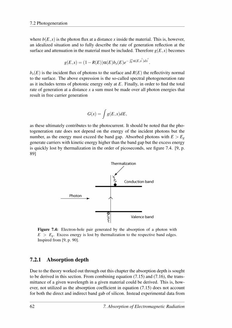
7.2 Photogeneration
Photogeneration dominates the generation processes of a photovoltaic device underillumination. The process is, however, not the only optical process occurring in aphotovoltaic device. Some light may be scattered without being absorbed at all.Some photons may transfer their energy to raise the kinetic energy of already mo-bile carriers and some may generate phonons, heat, to the system. The rate of thephotogeneration is sought in the following.
A slab of thickness x is considered exposed to the light intensity Io, see figure7.3.
Figure 7.3: A slab of thickness x and absorption coefficient α is exposed from theleft to the intensity Is. A portion is reflected as RIs, and a portion is exponentiallyattenuated through the material depicted by the exponentially decaying line drawn.Inspired from [9, p. 89].
As the light intensity passes through the material it is attenuated and this is describedusing the absorption coefficient α. A ray of photons with energy E and intensity Isis considered at normal incidence to a surface of a given absorbing material. If ittravels an infinitesimal distance dx a fraction α(E)dx of the incident light of energyE is absorbed. The light intensity I(x) is then attenuated by a factor e−α(E)dx. Thechange in intensity over traveled distance in the material is thus
dIdx
=−αI.
Integrating this over a none uniform α yields
I(x) = I(0)e−∫ x
0 α(E,x′)dx′,
where I(0) is the intensity just inside of the slab.If the light travels a distance x the intensity inside the slab is given by Lambert-
Beer’s Law, α being uniform, as
I(x) = I(0)e−αx (7.16)
It is now assumed all photons are absorbed by the material generating free carriers.At a distance x below the surface the rate of carrier generation per unit volume is
g(E,x) = b(E,x)α(E,x),
7. Absorption of Electromagnetic Radiation 61
7.2 Photogeneration
where b(E,x) is the photon flux at a distance x inside the material. This is, however,an idealized situation and to fully describe the rate of generation reflection at thesurface and attenuation in the material must be included. Therefore g(E,x) becomes
g(E,x) = (1−R(E))α(E)bs(E)e−∫ x
0 α(E,x′)dx′.
bs(E) is the incident flux of photons to the surface and R(E) the reflectivity normalto the surface. The above expression is the so-called spectral photogeneration rateas it includes terms of photonic energy only at E. Finally, in order to find the totalrate of generation at a distance x a sum must be made over all photon energies thatresult in free carrier generation
G(x) =∫
g(E,x)dE,
as these ultimately contributes to the photocurrent. It should be noted that the pho-togeneration rate does not depend on the energy of the incident photons but thenumber, as the energy must exceed the band gap. Absorbed photons with E > Eggenerate carriers with kinetic energy higher than the band gap but the excess energyis quickly lost by thermalization in the order of picoseconds, see figure 7.4. [9, p.89]
Figure 7.4: Electron-hole pair generated by the absorption of a photon withE > Eg. Excess energy is lost by thermalization to the respective band edges.Inspired from [9, p. 90].
7.2.1 Absorption depth
Due to the theory worked out through out this chapter the absorption depth is soughtto be derived in this section. From combining equation (7.15) and (7.16), the trans-mittance of a given wavelength in a given material could be derived. This is, how-ever, not utilized as the absorption coefficient in equation (7.15) does not accountfor both the direct and indirect band gab of silicon. Instead experimental data from
62 7. Absorption of Electromagnetic Radiation

7.3 Recombination processes
[5] of the imaginary part of the refractive index will be used for calculations of thetransmittance of a given wavelength. This is done to give an estimate of a reason-able junction depth. The electric field of an electromagnetic wave can be written as[7, p. 46]
~E = ~E0ei(ωt−~k·~r+ϕ), (7.17)
where E0 is the amplitude of the electric field, ω is the angular frequency, t is thetime, ~k is the wave vector, ~r is the spatial position, and ϕ is the phase. As it isassumed that the medium does not change in time, the first term of the argumentcan be excluded. Furthermore the phase is set to zero. Thus equation (7.17) in thez-direction reduces to
E = E0e−ikz. (7.18)
The relations k = nω
c , n = n− iκ[7, p. 68], ω = 2πν, and c = λν used in equation(7.18) yields
E = E0e−i 2π
λ(n−iκ)z,
where λ is the wavelength and n and k are the real and imaginary parts of the re-fractive index of the surrounding medium, respectively. The intensity of the elec-tromagnetic field is
I ∝ |E|2 = I0e−4π
λκz,
where I0 is the amplitude of the incoming light. Thus the transmittance is given as
T =II0
= e−4π
λκz,
Figures 7.5(a) and 7.5(b) show plots of the transmittance in a slab of silicon as afunction of distance from the silicon surface and wavelength. The transmittance isshown in units of (1−R) cf. figure 7.3
7.3 Recombination processes
Recombination is a process in which the mobile electrons do not contribute to thenet photo current but are lost by different removal mechanisms. One distinguishes
7. Absorption of Electromagnetic Radiation 63
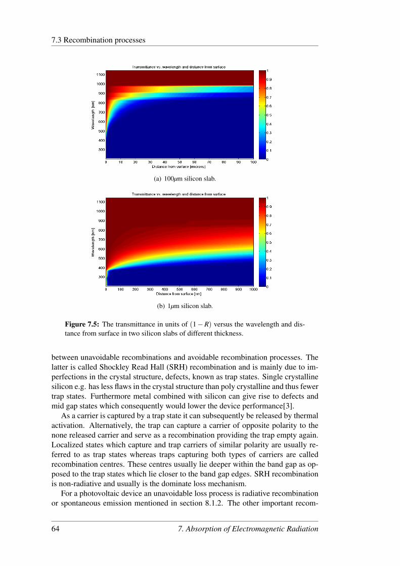
7.3 Recombination processes
(a) 100µm silicon slab.
(b) 1µm silicon slab.
Figure 7.5: The transmittance in units of (1−R) versus the wavelength and dis-tance from surface in two silicon slabs of different thickness.
between unavoidable recombinations and avoidable recombination processes. Thelatter is called Shockley Read Hall (SRH) recombination and is mainly due to im-perfections in the crystal structure, defects, known as trap states. Single crystallinesilicon e.g. has less flaws in the crystal structure than poly crystalline and thus fewertrap states. Furthermore metal combined with silicon can give rise to defects andmid gap states which consequently would lower the device performance[3].
As a carrier is captured by a trap state it can subsequently be released by thermalactivation. Alternatively, the trap can capture a carrier of opposite polarity to thenone released carrier and serve as a recombination providing the trap empty again.Localized states which capture and trap carriers of similar polarity are usually re-ferred to as trap states whereas traps capturing both types of carriers are calledrecombination centres. These centres usually lie deeper within the band gap as op-posed to the trap states which lie closer to the band gap edges. SRH recombinationis non-radiative and usually is the dominate loss mechanism.
For a photovoltaic device an unavoidable loss process is radiative recombinationor spontaneous emission mentioned in section 8.1.2. The other important recom-
64 7. Absorption of Electromagnetic Radiation
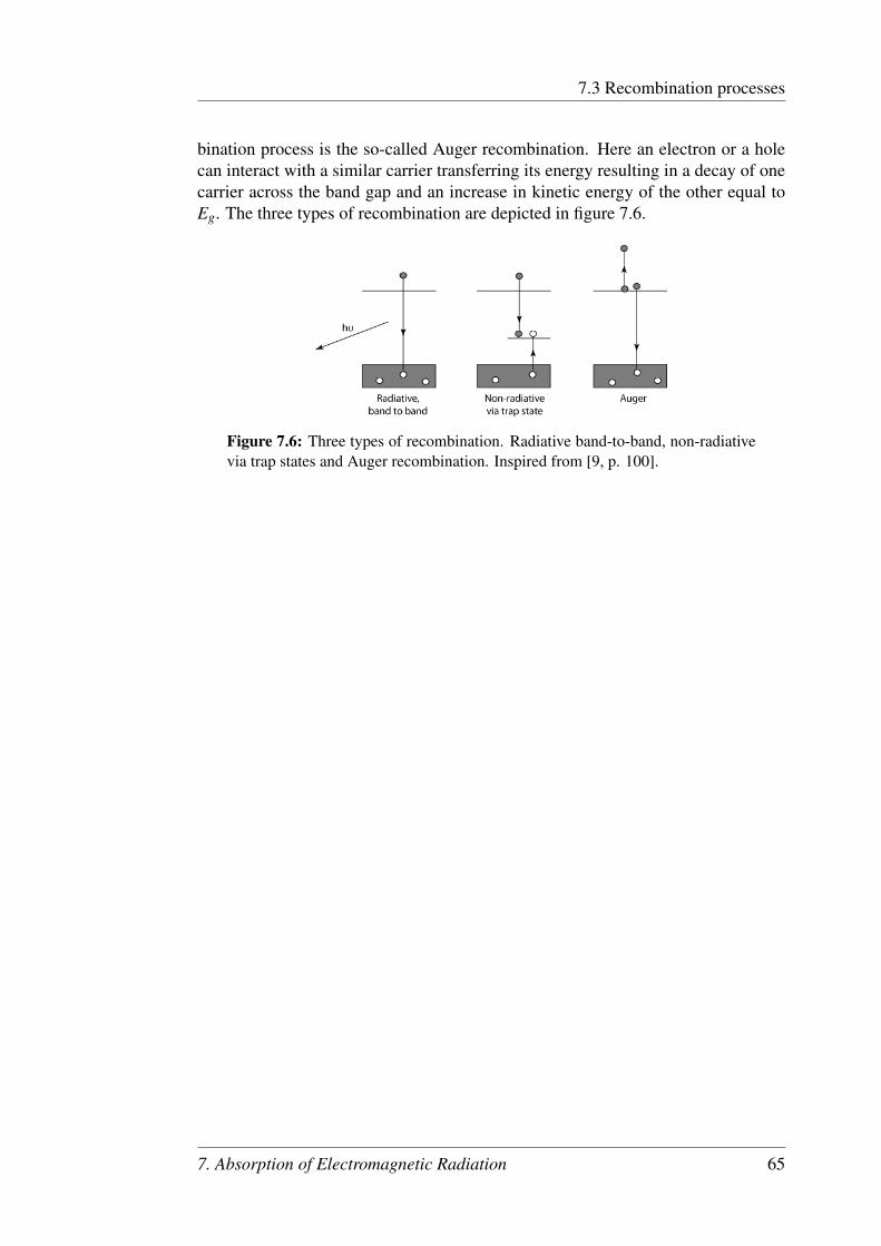
7.3 Recombination processes
bination process is the so-called Auger recombination. Here an electron or a holecan interact with a similar carrier transferring its energy resulting in a decay of onecarrier across the band gap and an increase in kinetic energy of the other equal toEg. The three types of recombination are depicted in figure 7.6.
Figure 7.6: Three types of recombination. Radiative band-to-band, non-radiativevia trap states and Auger recombination. Inspired from [9, p. 100].
7. Absorption of Electromagnetic Radiation 65

7.3 Recombination processes
66 7. Absorption of Electromagnetic Radiation

Chapter 8
Solar Cell Characteristics
This chapter deals with the concept of a photovoltaic device and the limitations thatarise when converting solar energy into electrical energy. Many factors have moreor less impact on the efficiency that can be obtained when converting solar energy.
8.1 Detailed balance
As explained in Section 6.1 excited electrons in the pn-junction need to not recom-bine to the valence band and must be extracted to an external circuit to obtain aphotocurrent. The efficiency by which solar energy is converted to electrical en-ergy, i.e. the photocurrent, in the cell is affected by various limiting factors.
A fundamental physical limitation arises due to the principle of so-called de-tailed balance. The solar cell does not only absorb solar radiation it also exchangesheat, thermal radiation, with its surroundings. The solar cell and its surroundingsradiate long wavelength thermal photons due to their finite temperature. To obtaina constant electron concentration in steady state the cell absorption rate must matchthat of photon emission.[9, p. 24]
8.1.1 Cell in the Dark
Under no illumination the cell will reach a thermal equilibrium with the ambient,which is assumed to radiate like a black body at a temperature Ta. The flux ofphotons on the surface of the solar cell at point s can be written using Planck’sradiation law as [9, p.18]
βa(E,~s,θ,ϕ)dΩ.d~SdE =2
h3c2
(E2
eE/kBTa−1
)dΩ.d~SdE,
where d~S is the element of surface area around ~s and dΩ the unit of solid anglearound the direction of emitted light which depends on (θ,φ).
67

8.1 Detailed balance
Considering the solar cell as a flat plate the incident flux normal on the surface,assuming the ambient radiation is received over a hemisphere and that the tempe-rature at all points ~s on the surface of the black body is equal, ~s can be excluded,yielding
ba(E) =2π
h3c2
(E2
eE/kBTa−1
).
The current density due to absorption of ambient radiation can be written as
jabs(E) = q(1−R(E))a(E)ba(E) (8.1)
where R(E) is the probability of photon reflection and a(E) is the probability ofabsorption of a photon of energy E. It is assumed that each photon of energy Egenerates one equivalent electron contributing to the current density jabs(E). Thequantity a(E) is known as the absorptivity of the cell and depends on the absorptioncoefficient of the material and the optical path length through it. Finally to obtainthe current due to ambient photon absorption equation (8.1) needs to be integratedover the dimensions of the surface of the solar cell.
The solar cell also emits thermal photons by spontaneous emission which isneeded to maintain a steady state and thus a constant electronic charge concentrationas mentioned above. When the cell is in thermal equilibrium with its surroundingsit emits thermal photons characteristic of its finite temperature Ta. The probabilityof emission of a photon with energy E through the cell’s surface is known as itsemissitivity ε. The corresponding current density of the photon emission is thengiven by
jrad(E) = q(1−R(E))ε(E)ba(E) (8.2)
Comparing the two terms of equation (8.1) and (8.2) the densities jabs and jrad mustbe equal to maintain the criteria of steady state. This implies that ε(E) = a(E). Inother words the rate of absorption must equal the rate of spontaneous emission andis a result of detailed balance. [9, p. 24-26]
8.1.2 Cell under illumination
If the cell is illuminated by a solar photon flux bs(E) it absorbs photons at a rate
(1−R(E))a(E)bs(E),
68 8. Solar Cell Characteristics
8.1 Detailed balance
where the similarity is seen to that of the rate of ambient absorption in equation(8.1). The corresponding current density due to illumination includes thus both acontribution from thermal and solar photons,
jabs(E) = q(1−R(E))a(E)(
bs(E)+(
1− Fs
Fe
)ba(E)
)The reducing fraction of Fs
Feto ba(E) arises due to a part of the incident ambient flux
is replaced by solar radiation.The solar illumination will excite a part of the electron population of the cell
resulting in a raised system chemical potential, ∆µ > 0. Due to a higher populationin the excited state spontaneous emission is increased as a direct consequence witha rate determined by ∆µ. The spectral flux of photons by a system at temperatureTc and chemical potential µ into a medium of refractive index ns, using Planck’sgeneralized radiation law, is [9, p.27]
β(E,s,θ,ϕ) =2n2
sh3c2
E2
e(E−∆µ)/kBTc−1(8.3)
By integrating over the solid angle of which photons can escape from the cell andusing n0 = 1, air at the surface, equation (8.3) reduces to
be(E,∆µ) =2π
h3c2E2
e(E−∆µ)/kBTc−1
As for the cell in the dark the emissitivity is denoted ε of the illuminated cell andthe current density for photon emission is thus
jrad(E) = q(1−R(E))ε(E)be(E,∆µ). (8.4)
Studying equation (8.4) it is clearly seen that it reduces to equation (8.2) for thecell in equilibrium with its surroundings in the dark, where a = ε and µ > 0. It is,however, less obvious how a(E) relates to ε(E) when ∆µ > 0. The equal sign stillholds though for a chemical potential that is constant through the device, but willnot be shown here. [9, p.28]
To obtain the highest possible net current for a cell under illumination jabs(E) issubtracted from jrad(E), which makes good sense as jrad(E) is a loss in the process.The net current then becomes
jabs(E)− jrad(E) = q(1−R(E))a(E)(
bs(E)+(
1+Fs
Fa
)ba(E)−be(E,∆µ)
)(8.5)
8. Solar Cell Characteristics 69

8.2 Characteristics of a solar cell
To gain a better view on the expression it is divided into two terms. The first con-cerns the net absorption in excess of that at equilibrium:
jabs(net) = q(1−R(E))a(E)(
bs(E)−Fs
Feba(E)
). (8.6)
The term to the right of the equal sign before the large brackets is simply the re-peating one in all the densities from earlier calculated. In the large brackets the firstterm is the flux of solar photons and the second is the fraction of thermal photonsthat have been replaced by solar photons.
The second contributing term of equation (8.5) is the net emission also called theradiative recombination current density,
jrad(net)(E) = q(1−R(E))a(E)[be(E,∆µ)−be(E,0)]
where ba(E) = be(E,0) as the chemical potential would be zero. The term in squarebrackets accounts for the difference between the radiation of a surface with ∆µ > 0to that of the incident flux of thermal photons normal to the surface.
The radiative recombination in the cell is an unavoidable loss process that lowersthe efficiency of the cell as the solar energy absorbed cannot be fully converted intoelectrical energy and i.e. fed to an external circuit. [9, p. 26-28]
8.2 Characteristics of a solar cell
In the previous section the radiative recombination was found to be accounting forlowering the maximum efficiency of converting solar rays into electrical energy.With the knowledge outlined, however, the absolute limiting efficiency can be cal-culated. A simple two-band system is considered where the ground state is com-pletely filled and the excited is empty, see figure 8.1.
The two bands are separated by a band gap Eg, where the promotion of an electronto the excited state cannot occur for an incident solar quantum with E < Eg. It isfurthermore assumed that the electrons in each band are in a quasi thermal equilib-rium at a temperature Ta from the surroundings and the chemical potential of thei’th band is µi.
8.2.1 Short circuit current
As the solar cell is under illumination it absorbs a net flux of photons that excitesome of the electron population. Due to the field at the pn-junction the electronsare separated from their holes and can thus be fed to an external circuit creating aphotocurrent. The angular range of the sun compared to the ambient is negligibleand therefore the second term Fs
Feba(E) in equation (8.6) can be excluded without
violation.
70 8. Solar Cell Characteristics

8.2 Characteristics of a solar cell
Figure 8.1: A two band system with an energy gap of Eg. Photons with E ≥ Eg
promote electrons to the excited state but for E >> Eg excess energy is quicklylost as heat to the system as the carriers relax to the band edges. Inspired from [9,p. 29]
An expression for the photocurrent density in a circuit can be obtained by inte-grating jabs from equation (8.6) over all photon energies. Furthermore the proba-bility of collecting an excited electron to the circuit is introduced as ηc(E) whichyields the short circuit current density
Jsc = q∫
∞
0ηc(E)(1−R(E))a(E)bs(E)dE.
In the ideal case of a maximum efficient solar cell it is assumed that the material isperfectly absorbing, non-reflecting so each photon with E > Eg contributes to thepromotion of exactly one electron to the upper excited state. Radiative recombi-nation cannot be neglected, however, and is an unavoidable loss. The remainingelectrons are assumed to be perfectly separated from their holes and thus collectedby the negative terminal of the cell, ηc(E) = 1. Using the above assumptions andutilizing
a(E) =
1 E ≥ Eg0 E < Eg
,
the maximum photocurrent for the particular band gap can be reduced to the expres-sion
Jsc = q∫
∞
Eg
bs(E)dE.
The photocurrent is now only a function of the size of the band gap and the incidentsolar spectrum. It is clear that Jsc will increase as Eg decreases and in order todetermine the actual efficiency of conversion the spectrum must be defined.
8. Solar Cell Characteristics 71

8.2 Characteristics of a solar cell
8.2.2 Open circuit voltage
Applying a bias over the cell in the dark results in a so-called dark current thatflows through the device. The dark current acts in the opposite direction of thephotocurrent and lowers the net current. The J(V ) characteristic can be written as
J(V ) = Jsc− Jdark(V ),
as J is a function of applied potential.Most solar cells behave like diodes in the dark and the reverse current density has
the form Jdark(V ) = J0(eqV/kBT −1), where J0 is a temperature dependent constant.The term qV is the chemical potential ∆µ of the cell, assuming the material is idealwith lossless carrier transport. As the cell is illuminated by solar photons there isa contribution from the photocurrent and reverse current due to applied bias. Thereverse current in the dark compared to that under illumination, however, is notformally equal, but for many photovoltaic materials they are approximately identicaland the J(V ) characteristic still holds as
J(V ) = Jsc− J0(eqV/kBT −1). (8.7)
The open circuit voltage Voc is the maximum value the potential difference canreach. This is achieved when the contacts are isolated, where the dark current andthe short circuit photocurrent cancel out. Thus from equation (8.7) Voc is
0 = Jsc− J0(eqVockBT −1)
Voc =kBT
qln(
Jsc
J0
). (8.8)
According to equation (8.8) the open circuit voltage increases logarithmically withthe light intensity. The point Voc is shown in figure 8.2, from which it also canbe seen, that for V < 0 the cell consumes power to generate a photocurrent, for0 < V < Voc the cell creates power, and for V > Voc the cell is power consumingagain. [9, p. 10-11+30-31]
8.2.3 Parasitic resistances
In a real solar cell the contact between metal and semiconducting material and thefact that current leaks around the sides of the device acts as resistances. Electricallythis corresponds to a shunt resistance in parallel and a resistance in series with thecell, which is illustrated in figure 8.3.
The series resistance arises due to the resistance of the cell material and the con-tacts. A large series resistance is problematic for high current densities. Optimallythe series resistance is to be as low as possible. The shunt resistance arises dueto leakage of current through the cell, around the edges of the device and between
72 8. Solar Cell Characteristics

8.2 Characteristics of a solar cell
Figure 8.2: I-V characteristic of an ideal diode under illumination and in the dark.Inspired from [9, p.10]
Figure 8.3: Illustrates a circuit model of a solar cell. Inspired from [9, p. 14].
8. Solar Cell Characteristics 73

8.3 Efficiency
contacts of different polarity. The shunt resistance should be as high as possible.If the parasitic resistances are included the diode equation from equation (8.7) ismodified to [9, p.14]
J = Jsc− J0
(eq(V+JARs)/kBT −1
)− V + JARs
Rsh
Here A is the surface area of which J passes through. The effect of increasing seriesresistance and decreasing shunt resistance on an I-V curve is shown in figure 8.4.
Figure 8.4: I-V characteristic of a solar cell where a decrease in shunt resistanceand an increase in series resistance lowers the total output of the cell. Inspiredfrom [9, p.14].
8.3 Efficiency
As described in Section 8.2.2 a solar cell delivers power in the range of bias from 0to Voc. The power density can be written as
P = JV (8.9)
The maximum efficiency is reached at a voltage Vm with a corresponding currentdensity Jm. The fill factor FF describing the squareness of the J-V curve is definedas
FF =JmVm
JscVoc. (8.10)
In figure 8.5 Vm, Voc, Jm, Jsc are shown, where the area of the inner and outer rectan-gle is drawn by Vm× Jm and Voc× Jsc, respectively. Thus the fill factor is illustratedby the ratio between the inner and outer rectangle. The efficiency of a cell is givenas a fraction of the maximum power density delivered by the cell to the incidentlight power density
η =Pm
Ps=
JmVm
Ps=
JscVocFFPs
,
74 8. Solar Cell Characteristics

8.3 Efficiency
Figure 8.5: Current-voltage (thick) and power-voltage (narrow) characteristics ofan ideal cell. The maximum power density occurs at maximum bias Vm. It canbe calculated by multiplying Jm and Vm and is also given by the area of the innerrectangle. The outer rectangle has the area Jsc×Voc. A fill factor FF of 1 wouldequal the extreme case of the current voltage curve following the outer rectangle.Inspired from [9, p.12].
where equations (8.9) and (8.10) have been used. Voc, Jsc, FF , and η are the four keycharacteristics of a solar cell, and should be determined for particular illuminationconditions.
As a consequence maximum efficiency must be achieved when
d(J(V )V )
dV= 0.
In the simplified case in the above theory outlined, the efficiency of the two bandphoto converter is only a function of the band gap Eg and the incident spectrum.Furthermore the power conversion efficiency η is a function of only the band gapsize if the incident spectrum is fixed. In this situation it is seen that very small andvery large band gaps make poor photo converters. In the first situation a very smallband gap leads to a low working value of V because Vm is always less than Eg. In thelatter case the majority of incident photons do not have enough energy to promotethe electrons from the lower band resulting in a poor photocurrent.
The efficiency versus band gap calculated from a standard solar spectrum isshown in figure 8.6 with a maximum of 33% at an Eg of 1.4eV. From [9, p. 33]
Typical material compounds possessing these high efficiencies are galium arsenideand indium phosphide due to their band gaps lying close to the optimum value.These compounds, however, are expensive compared to the much more abundantsilicon based solar cells with a band gap at 1.17eV. This value is not favourable forhigh efficiency cells and an efficiency of app. 29% has been achieved as a highefficiency value. [9, p. 36]
8. Solar Cell Characteristics 75

8.3 Efficiency
Figure 8.6: Efficiency versus band gap size calculated for a standard solar spec-trum. Maximum of 33% at an Eg around 1.4eV . From [9, p. 33]
8.3.1 Spectrum influence on efficiency
In order to determine the effect the incident spectrum has on the efficiency of thephoto conversion a representative model is used. The sun is replaced with a blackbody at temperature Ts=5760K as illuminating source. This model predicts a limit-ing efficiency of around 31% at a band gap of 1.3eV, calculated by [9, p. 34]. If theradiating source red shifts its spectrum it results in lower energy radiated and over-all it decreases the optimum band gap and the limiting efficiency. In the extremecase of Ts = Ta, where Ta is the cell temperature, the cell is in thermal equilibriumwith the source and no net photo conversion occurs. Raising the temperature ofthe source relatively to the cell increases the efficiency as a direct consequence. IfTa→ 0 the cell does not experience any radiative recombination as the spontaneousemission has vanished at this extremum.
With this assumption and if all carriers are collected to the external circuit con-tributing with ∆µ = qV the maximum efficiency is given by
η =Eg
∫∞
0 bs(E)dE∫∞
0 Ebs(E)dE.
The term in the top of the fraction accounts for the energy that is absorbed above Egand the bottom of the fraction is simply all incident energy. The theoretical maxi-mum has been reported by Shockley and Queisser [9, p. 35] to around 44% with aband gap at 2.2eV and a modelled black body sun at 6000K. This value is calculatedto be the ultimate efficiency to be obtained from a photovoltaic device. However,cooling down the cell requires energy which again reduces the net efficiency.
Another method to improve the efficiency is to concentrate the solar rays thathit the surface of the cell. The angular range subtended by the sun is focused ontothe cell surface resulting in a larger absorbed flux yielding a larger photocurrent.The cell emits radiation in all directions but only absorbs in a narrow angular rangefrom the sun. A result of increasing the angular range is a more effective balancebetween the two contributions to the photocurrent.
76 8. Solar Cell Characteristics
8.3 Efficiency
To summarize, a lot of limitations decrease the maximum efficiency that can beobtained by the solar cell. Incomplete absorption of incident light due to reflectionat the surface and furthermore some light travels through the device which reducesthe photocurrent. Excited electrons can be trapped at defect sites as the crystalstructure of the material is not perfect and recombine before being collected to theexternal circuit.[9, p. 35]
8. Solar Cell Characteristics 77

8.3 Efficiency
78 8. Solar Cell Characteristics

Chapter 9
Solar Cell Fabrication
This chapter contains the fabrication methods utilized to construct the silicon solarcells. Phosphorus is screen printed on p-type multi crystalline silicon and phospho-rus is deposited using a spin-on method.
The solar cells to be constructed are all based on p-type polycrystalline silicon witha resistivity of 1,8-4,5Ωcm and a thickness of 750µm. Furthermore substrates of15-20Ωcm have been used for examination. The general structure of a cell consistsof four layers. The top layer is an aluminum contact with a designed pattern that al-lows radiation to reach the two layers below containing the pn-junction. Accordingto figure 7.5 an ideal junction depth should lie in the range between app. 200-400nmfor the depletion layer to lie in the vicinity of a relatively high absorption. However,the junction cannot be too shallow as defects near the surface give rise to recombi-nation centres. Finally the bottom layer consist of an aluminum backside contact.See figure 9.1 for schematic setup of the four layers.
Figure 9.1: Illustrates the four basic layers of the solar cells fabricated.
9.1 pn-junction formation
In order to construct a solar cell a pn-junction needs to be formed inside a semi-conducting material. The intrinsic property of a band gap in the semiconductingmaterial is needed for the generation of electron-hole pairs that are created under
79

9.1 pn-junction formation
illumination, see section 6. The pn-junction formation was conducted by the diffu-sion of phosphorus into the above mentioned p-type silicon substrates. Two meth-ods were used for adding the phosphorus paste onto the silicon substrates.
9.1.1 Phosphorus application onto p-type silicon
The first method utilized a screen-printing technique in which a stainless steel mesh(Fe/Cr18/Ni10/Mo3), 180 mesh per inch from Advent Research Materials Ltd, wasused. The mesh was fixed in a metal frame depicted in figure 9.2.
Figure 9.2: Illustrates the steel mesh to the left and the platform rack to the righton which the substrates are placed.
The screen printing setup was constructed for the application of 1x1 or 1x2cm sil-icon substrates, which were placed onto either a 1x1 or 1x2cm platform. The steelmesh was placed on top of the substrates with a distance of 1-2mm to enable theadding of phosphorus screen printing paste (Filmtronics) onto the silicon, see figure9.3 for application setup.
Figure 9.3: Illustrates the application of phosphorus using the screen printingtechnique.
The phosphorus was added by pouring down a droplet at one end of the mesh andthen scraped over the mesh to cover the silicon substrate entirely. The amountof paste added on the substrate depended on the pressure at which the paste wasscraped and was not entirely consistent. After the application of phosphorus thesubstrates were heated on a plate for 15min at 150C.
80 9. Solar Cell Fabrication
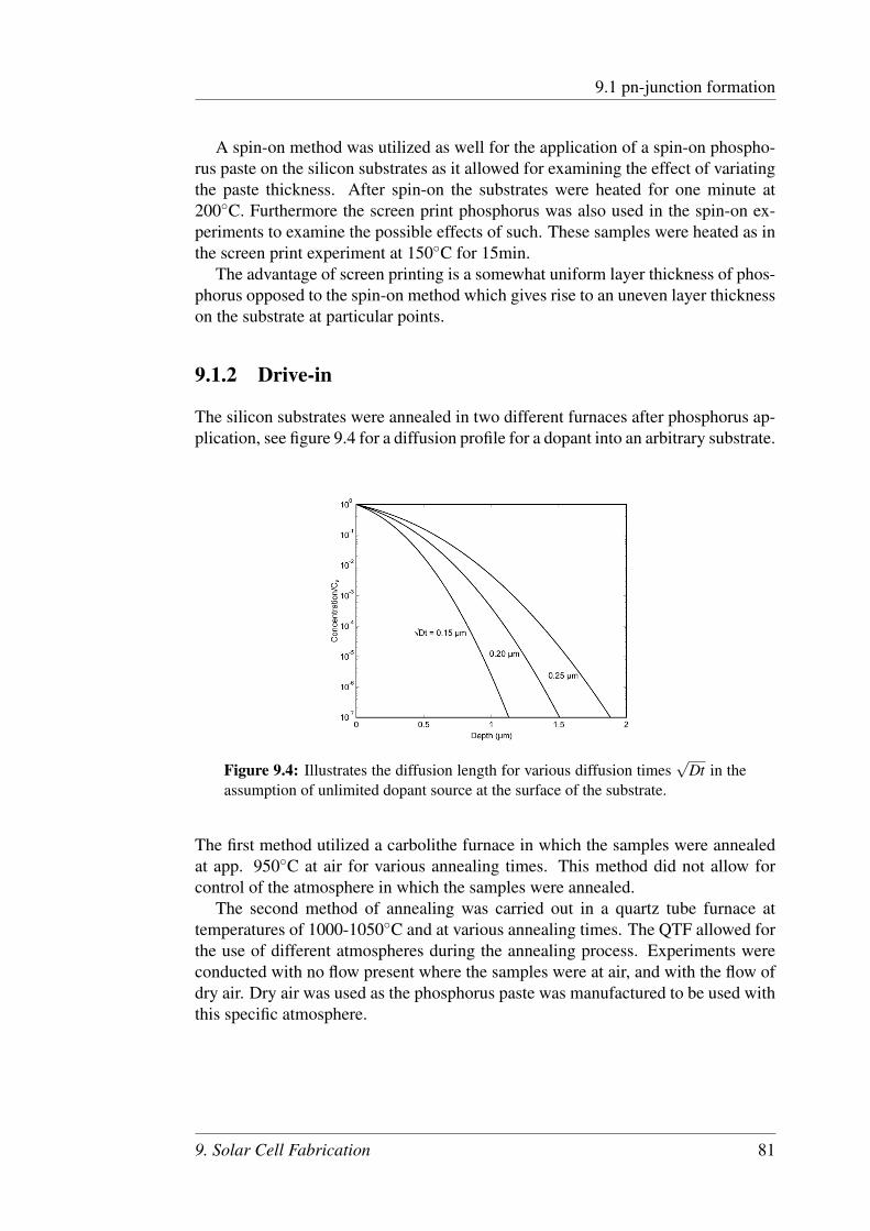
9.1 pn-junction formation
A spin-on method was utilized as well for the application of a spin-on phospho-rus paste on the silicon substrates as it allowed for examining the effect of variatingthe paste thickness. After spin-on the substrates were heated for one minute at200C. Furthermore the screen print phosphorus was also used in the spin-on ex-periments to examine the possible effects of such. These samples were heated as inthe screen print experiment at 150C for 15min.
The advantage of screen printing is a somewhat uniform layer thickness of phos-phorus opposed to the spin-on method which gives rise to an uneven layer thicknesson the substrate at particular points.
9.1.2 Drive-in
The silicon substrates were annealed in two different furnaces after phosphorus ap-plication, see figure 9.4 for a diffusion profile for a dopant into an arbitrary substrate.
Figure 9.4: Illustrates the diffusion length for various diffusion times√
Dt in theassumption of unlimited dopant source at the surface of the substrate.
The first method utilized a carbolithe furnace in which the samples were annealedat app. 950C at air for various annealing times. This method did not allow forcontrol of the atmosphere in which the samples were annealed.
The second method of annealing was carried out in a quartz tube furnace attemperatures of 1000-1050C and at various annealing times. The QTF allowed forthe use of different atmospheres during the annealing process. Experiments wereconducted with no flow present where the samples were at air, and with the flow ofdry air. Dry air was used as the phosphorus paste was manufactured to be used withthis specific atmosphere.
9. Solar Cell Fabrication 81

9.2 Contacts
9.2 Contacts
Firstly the oxide layer formed from the drive-in process had to be removed, whichwas done in hydrofluoric acid. The front and backside contacts on the solar cellswere fabricated followingly using two different techniques. The first approach uti-lized photolithography where a positive photoresist of the type ma-P 1205 was spunat 1000 rmp onto the top n-type layer and dried at two minutes at 120C on a hotplate. A mask is put on top of the resist, see figure 9.5, and the positive resist isexposed to uv-radiation for one minute at 32W in order to form a contact patternthat allows for light to reach the active solar cell area. The exposed resist on the
Figure 9.5: Front contact mask
substrate is then removed using a photoresist developer type ma-D 331.Afterwards app. 200nm aluminum was sputtered on as conductor. The layer was
formed in a sputter coater at a vacuum of 8-9·10−6mbar. Finally lift-off is executedin an ultra sound bath of acetone. The backside pattern was constructed similarlyin order to cover the whole backside of the solar cell with aluminum but leave onemillimeter unexposed along each side to avoid short circuiting from the front sideto the backside contacts. In addition the solar cells were polished along the sideswith fine sandpaper as the sputtering process would leave aluminum on the sidesof the wafer which increases the risk of contacting the wrong layers. However, thistreatment was not consistent to prove that the aluminum at the sides had vanishedcompletely.
To avoid the issue of short circuit along the sides due to aluminum a metalmask was constructed to cover the substrates with contact patterns, see figure 9.6.Furthermore after the spin-on process the phosphorus tended to accumulate to a cer-
Figure 9.6: Metal mask with contact patterns for front and backside.
tain extent on the sides of the wafers resulting in a short circuit between the n-side
82 9. Solar Cell Fabrication

9.2 Contacts
Figure 9.7: Illustrates the solar cell with the n-type layer short circuited to thebackside contact due to phosphorus accumulating at the sides of the substratesafter the spin-on process.
and the backside contact, see figure 9.7. The ideal situation of the separation of thefour basic layers is depicted in figure 9.1.
To try and resolve this issue Reactive Ion Etching was used to separate the n-sidelayer from the backside contact, see figure 9.8. This was done by firstly spinningon a photo resist on the substrates after the hydrogen termination process. The
Figure 9.8: Illustrates the concept of the RIE process where the n-type layer isseparated from the back side contact to prevent short circuiting the solar cell.
substrates were heated on a hot plate for two minutes at 120C. Afterwards the sub-strates were exposed to uv-radiation for 80sec at 32W using a mask that left 2mmalong each side of the substrate exposed. The substrates were developed as in sec-tion 9.2 leaving 2mm along each side of the substrate prepared for the RIE-etching.The etching depth was hence examined in a profiler to app. 4µm, which succeedsthe depth of the n-doped layer.
9. Solar Cell Fabrication 83

9.2 Contacts
84 9. Solar Cell Fabrication

Chapter 10
Characterization Methods
This chapter presents the different characterization methods used to study the fab-ricated solar cells from Chapter 9.
10.1 Sheet resistance
Sheet resistance measurements were conducted after the oxygen removal processdescribed in section 9.2. The technique is simple and gives a direct estimate ofthe dopant concentration in the substrate and also how far from the surface thejunction is located. A high sheet resistance results in a low dopant concentrationand a shallow junction level and vice verca. The experimental theory can be seenin section 4.2 where the collinear four point probe approach is utilized, see figure10.1.
Figure 10.1: Collinear four point probe approach utilized to determine the sheetresistance.
85
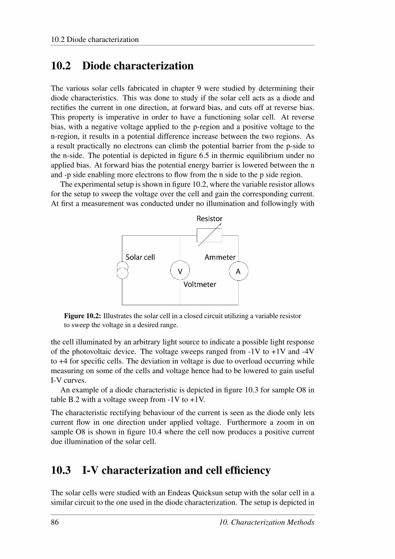
10.2 Diode characterization
10.2 Diode characterization
The various solar cells fabricated in chapter 9 were studied by determining theirdiode characteristics. This was done to study if the solar cell acts as a diode andrectifies the current in one direction, at forward bias, and cuts off at reverse bias.This property is imperative in order to have a functioning solar cell. At reversebias, with a negative voltage applied to the p-region and a positive voltage to then-region, it results in a potential difference increase between the two regions. Asa result practically no electrons can climb the potential barrier from the p-side tothe n-side. The potential is depicted in figure 6.5 in thermic equilibrium under noapplied bias. At forward bias the potential energy barrier is lowered between the nand -p side enabling more electrons to flow from the n side to the p side region.
The experimental setup is shown in figure 10.2, where the variable resistor allowsfor the setup to sweep the voltage over the cell and gain the corresponding current.At first a measurement was conducted under no illumination and followingly with
Figure 10.2: Illustrates the solar cell in a closed circuit utilizing a variable resistorto sweep the voltage in a desired range.
the cell illuminated by an arbitrary light source to indicate a possible light responseof the photovoltaic device. The voltage sweeps ranged from -1V to +1V and -4Vto +4 for specific cells. The deviation in voltage is due to overload occurring whilemeasuring on some of the cells and voltage hence had to be lowered to gain usefulI-V curves.
An example of a diode characteristic is depicted in figure 10.3 for sample O8 intable B.2 with a voltage sweep from -1V to +1V.
The characteristic rectifying behaviour of the current is seen as the diode only letscurrent flow in one direction under applied voltage. Furthermore a zoom in onsample O8 is shown in figure 10.4 where the cell now produces a positive currentdue illumination of the solar cell.
10.3 I-V characterization and cell efficiency
The solar cells were studied with an Endeas Quicksun setup with the solar cell in asimilar circuit to the one used in the diode characterization. The setup is depicted in
86 10. Characterization Methods

10.3 I-V characterization and cell efficiency
Figure 10.3: Diode characteristic of sample O8 from -1V to +1V. The rectify-ing behavior of the current is observed as the diode only lets current flow in onedirection.
Figure 10.4: Illustrates a zoom in on sample O8 where the current rises abovezero due to the irradiation of light at the solar cell surface. The cell hence producespower.
10. Characterization Methods 87

10.3 I-V characterization and cell efficiency
figure 10.5, where a xenon flash is utilized as the illuminating source with an effectof 1200W/m2. The spectrum of the xenon lamp approximately resembles that of the
Figure 10.5: Illustrates the solar cell in series with a variable resistor and ammeterand in parallel with a voltmeter, used in the efficiency measurement setup. [10]
sun, see figure 10.6, and to a certain extend this indicates how the solar cell wouldoperate under solar illumination.
Figure 10.6: Spectrum of the artificial light source used as illuminator during I-Vcharacteristics. The spectrum resembles that of the sun to a certain extend andtherefore indicates how the solar cell operates under solar illumination. [10]
The solar cell is in series with an ammeter and in parallel with a voltmeter andcurrent voltage characteristics is measured by sweeping from open circuit to shortcircuit while measuring the voltage current output. This output yields the I-V char-acteristic of the specific cell and the quantities Isc, Voc ,and the fill factor FF , out-lined in section 8.3. To determine the efficiency of the solar cell the irradiance ofthe flash is measured at a monitor cell and a computer program calculates the effectof the light flash arriving at the cell surface. The maximum power created by thesolar cell is determined by utilizing the quantities Vm and Im in Pm = Im ·Vm. Theefficiency is thus calculated by the ratio between the maximum power delivered bythe cell to the incident light power, η = Pm/Ps.
The I-V curve of a fabricated solar cell, sample O8 in table B.2, is shown infigure 10.7
88 10. Characterization Methods

10.3 I-V characterization and cell efficiency
Figure 10.7: Illustrates the I-V curve of sample O8 in table B.2
The I-V curve gives information about the shunt and series resistances that governsthe specific solar cell, as outlined in section 8.2.3. This information can be utilizedto establish whether the solar cell has contact problems i.e. a high series resistancewhich is a problem at high current densities. Additionally it yields informationabout the leakage current or shunt resistance in the cell that is a problem in poorlyrectifying devices. [9, p. 13-14]
10. Characterization Methods 89

10.3 I-V characterization and cell efficiency
90 10. Characterization Methods

Chapter 11
Results
In this chapter the characteristics of the solar cells, achieved by sheet resistance-,I-V-, and diode-measurements, are studied. These characteristics are discussed andpossible improvements are conducted. The experiments are presented chronologi-cally.
11.1 Drive-in atmosphere
By manufacture prescription, except for the paste application technique, four sam-ples were fabricated varying the spin-on speed between 1k and 2k rpm and drive-intime between 1.5min and 3min. As explained in section 9.1.2 drive in of spin-onscreen print phosphorus was at first conducted in a carbolithe furnace at app. 950Cat air. A 1% HF acid was used for oxide removal for 30sec before contacts werefabricated using photolithography described in section 9.2.
The diode characteristic of sample A2 spun at 1k rpm and a drive-in time of1.5min is shown in figure 11.1. Note that the red curve is due to illumination ofthe solar cell using a microscope lamp to investigate a photovoltaic response andthe blue curve is the dark current. If only a red curve has been displayed, this isfor the illuminated solar cell. It is seen that the solar cell exhibits some rectifyingdiode behavior, however, the insufficient current implies an issue with the seriesresistance of the solar cell. The corresponding I-V curve from the efficiency mea-surement is shown in figure 11.2, with an efficiency η = 0.1%. The efficiency hasbeen measured for the total area of the solar cell top surface, thus the area coveredby the front contact has not been accounted for in the efficiency calculations. Thisis consistent for all efficiency measurements.
As the dopant paste originally was fabricated to be utilized in a combination witha mesh screen at app. 200-400 mesh per inch, the issue could lie in a deviating pastethickness according to supplier prescription.
Samples B1-B4 were fabricated using the same conditions as in the above and inorder to apply a proper amount of dopant onto the substrates a mesh frame was con-structed, as outlined in section 9.1.1. However, the diode characteristics obtained
91

11.1 Drive-in atmosphere
Figure 11.1: Diode characteristic of sample A2.
Figure 11.2: I-V characteristic of sample A2 for measurements obtained by theuse of an artificial light source resembling the solar spectrum.
92 11. Results

11.1 Drive-in atmosphere
from using screen printing as phosphorus application technique did not reveal anyimprovement for the cell to act as a rectifying diode.
To resolve the problem of not gaining a proper diode behavior, a quartz tubefurnace was used in the drive-in process to enable manipulation of the atmosphere.This allowed for the use of a controlled dry air atmosphere which reduced the oxidelayer formation at the substrate surface in contrary to the drive-in process using thecarbolithe furnace, where the substrates were in a non-dry air atmosphere. The alter-ing of the particular atmosphere, lies in the composition of the phosphorus dopant.By conferring with the semiconductor-group in Aarhus, the drive-in temperaturewas increased to 1000C due to a more suitable diffusion profile. The concentrationof the HF acid was also increased from 1% to 10% to ensure complete removal ofthe oxide layer formed during drive-in.
A general issue when applying the phosphorus paste onto the substrates, bothin the spin-on and screen printing techniques, was the accumulation of paste alongthe edges of the samples. This could result in a low shunt resistance and possibly ashort circuit between the contacts as the n-doped region would directly connect thefront- and backside contacts. To prevent the paste from accumulating at edges ofthe samples, tape was placed along the sides of the samples covering app. 1mm ofthe substrate area from the edge before screen printing the phosphorus.
The initiatives discussed were implemented in the fabrication of the C-series.Figure 11.3 shows the diode characteristics measurement of sample C2, which isseen to exhibit no diode behavior and instead resemble a resistor.
At this stage the sheet resistance measuring method from section 10.1 was set
Figure 11.3: Diode characteristic of sample C2.
up and utilized. The aim was to investigate the diffusion of phosphorus into thesubstrates, as the sheet resistance gives a measure of the dopant concentration leveland the position of the pn-junction. If the pn-junction lies too close to the substratesurface metal defects from the front contact can act as recombination centres andthus reduce the net current generation Sample D was fabricated at the same condi-tions as sample B2 in order to measure the sheet resistance. The sheet resistance
11. Results 93

11.1 Drive-in atmosphere
of sample D was measured to 44.01Ω/sq. As a sheet resistance of app. 25Ω/sqis sought, the high value indicates drive-in issues. This sheet resistance value wassought by conferring with the semiconductor group in Aarhus.
The HF acid aims to remove the oxide layer formed during the drive-in process.If an oxide layer remains at the surface it will isolate the contacts from the solarcell. When all oxide has been removed the hydrogen from the acid forms covalentbonds to the silicon atoms at the surface. This leaves the surface highly hydropho-bic. Sample D was observed to not exhibit a hydrophobic surface and therefore itwas assumed that too much phosphorus had not contributed to the drive-in processand thus prevented the hydrogen to access the surface silicon atoms. This excessamount of phosphorus paste could also have an influence on the sheet resistancemeasurement.
Samples G1-G4 were fabricated by increasing drive-in times of 3, 5, 7, and 9minof identical phosphorus paste thickness to investigate the hydrophobicity of the sam-ples. G1 and G2 did not show any hydrophobic characteristics, while G3 and G4with a drive-in time of 7 and 9min, respectively, exhibited hydrophobic surfaces.The diode characteristics of sample G1 and G4 is shown in figure 11.4 and 11.5.Sample G1 and G4 show some diode behavior, however, the lack of rectificationcan be explained by the influence of a Schottky diode between metal and semicon-ductor. If this is the case the hydrophobicity of sample G4 has not contributed toa better contact between the metal and semiconductor. The variation of the diodebehavior of sample G4 compared to G1 must then lie in the different drive-in times.
Comparing sample G1 and C2 fabricated by the same specifications, it is seen
Figure 11.4: Diode characteristic of sample G1.
that the I-V curves show no resemblance. Thus the deviation was assumed to lie inthe placement of the samples in the QTF tubes as the placement method was non-consistent.
The drive-in procedure using the QTF was executed by placing the substrates inan inner tube which is slided into the main tube of the furnace. When inserted intothe main tube, with a temperature of 1000C, the inner tube will obtain the tempe-
94 11. Results
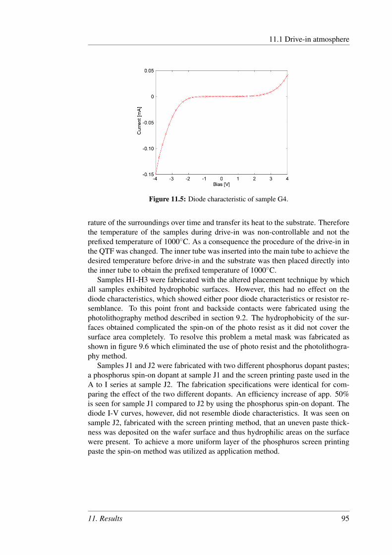
11.1 Drive-in atmosphere
Figure 11.5: Diode characteristic of sample G4.
rature of the surroundings over time and transfer its heat to the substrate. Thereforethe temperature of the samples during drive-in was non-controllable and not theprefixed temperature of 1000C. As a consequence the procedure of the drive-in inthe QTF was changed. The inner tube was inserted into the main tube to achieve thedesired temperature before drive-in and the substrate was then placed directly intothe inner tube to obtain the prefixed temperature of 1000C.
Samples H1-H3 were fabricated with the altered placement technique by whichall samples exhibited hydrophobic surfaces. However, this had no effect on thediode characteristics, which showed either poor diode characteristics or resistor re-semblance. To this point front and backside contacts were fabricated using thephotolithography method described in section 9.2. The hydrophobicity of the sur-faces obtained complicated the spin-on of the photo resist as it did not cover thesurface area completely. To resolve this problem a metal mask was fabricated asshown in figure 9.6 which eliminated the use of photo resist and the photolithogra-phy method.
Samples J1 and J2 were fabricated with two different phosphorus dopant pastes;a phosphorus spin-on dopant at sample J1 and the screen printing paste used in theA to I series at sample J2. The fabrication specifications were identical for com-paring the effect of the two different dopants. An efficiency increase of app. 50%is seen for sample J1 compared to J2 by using the phosphorus spin-on dopant. Thediode I-V curves, however, did not resemble diode characteristics. It was seen onsample J2, fabricated with the screen printing method, that an uneven paste thick-ness was deposited on the wafer surface and thus hydrophilic areas on the surfacewere present. To achieve a more uniform layer of the phosphuros screen printingpaste the spin-on method was utilized as application method.
11. Results 95

11.2 Sheet resistance vs. paste thickness
11.2 Sheet resistance vs. paste thickness
A series of samples with different phosphorus paste thickness were fabricated toexamine the influence of increasing paste thickness to the sheet resistance. Phos-phorus paste was spun on at various spin velocities onto a p-type silicon substrateand drive-in was executed, cf. the procedure in chapter 9. After oxide removal inHF acid the sheet resistance of the n-doped silicon layer was measured as mentionedin section 10.1. The results are shown in table 11.1.
It is seen from table 11.1 that an increase in paste thickness from 2.7 to 9µm
Sample Thickness Drive-in time Rsheet Hydrofobicity1 9.0µm 1.5min 23.25Ω/sq semi-hydrofobic2 7.0µm 1.5min 23.57Ω/sq semi-hydrofobic3 5.1µm 1.5min 21.53Ω/sq hydrofobic4 3.4µm 1.5min 23.80Ω/sq hydrofobic5 2.7µm 1.5min 22.44Ω/sq hydrofobic6 9.0µm 3min 16.77Ω/sq hydrofobic7 7.0µm 3min 16.95Ω/sq hydrofobic8 5.1µm 3min 17.09Ω/sq hydrofobic9 3.4µm 3min 16.95Ω/sq hydrofobic
10 2.7µm 3min 17.59Ω/sq hydrofobic
Table 11.1: Measurements of the sheet resistance of samples with different pastethickness and diffusion time.
does not alter the sheet resistance of the n-doped silicon layer. Hence, if the amountof phosphorus paste on the surface is not fully consumed, only the drive-in timeand temperature have an influence on the sheet resistance and thus the dopant con-centration and junction depth. A decreased drive-in time gives rise to an increasedsheet resistance revealing a lowering of dopant concentration or a shallow junctionor both combined. This is in accordance with the theory outlined in section 4.1.
11.3 Contact annealing
Generally the output current of the fabricated solar cells was low which results ina low efficiency as displayed in the tables in appendix B. To enhance the electricalconnection between the solar cell and the contacts four samples M1, M2, N1, andN2 were fabricated. M1 and N1 together with M2 and N2 were fabricated undersame conditions for the purpose of contact annealing the N series. The N series wasannealed in a QTF at 400C with an inert atmosphere of argon flow for 30min. Thediode characteristics of M2 and N2 are shown in figure 11.6 and 11.7, respectively.It is seen at sample N2 that a smaller bias is required to force a current compared
to the I-V curve of sample M2. The annealing procedure has therefore contributedto a better contact between the semiconductor and the metal and thus a lowering ofthe series resistance has occurred. This is also seen in the improvement in efficiency
96 11. Results

11.3 Contact annealing
Figure 11.6: Diode characteristic of sample M2.
Figure 11.7: Diode characteristic of sample N2, for which contacts have beenannealed.
11. Results 97
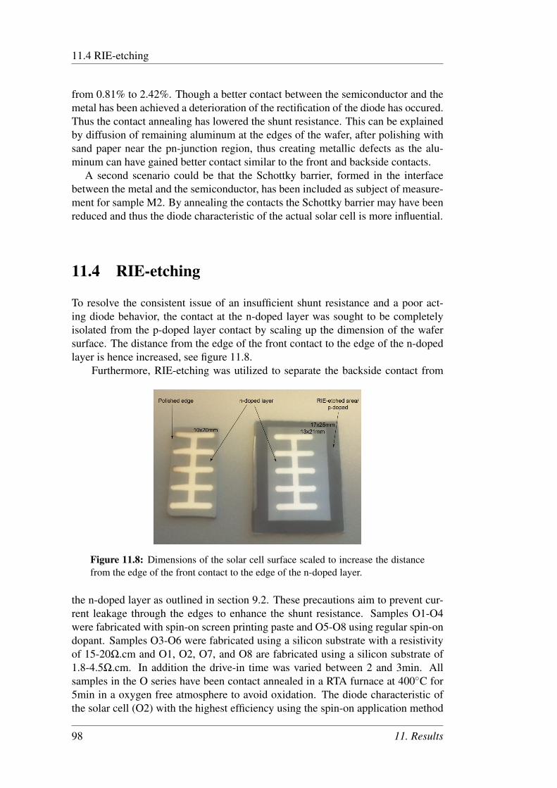
11.4 RIE-etching
from 0.81% to 2.42%. Though a better contact between the semiconductor and themetal has been achieved a deterioration of the rectification of the diode has occured.Thus the contact annealing has lowered the shunt resistance. This can be explainedby diffusion of remaining aluminum at the edges of the wafer, after polishing withsand paper near the pn-junction region, thus creating metallic defects as the alu-minum can have gained better contact similar to the front and backside contacts.
A second scenario could be that the Schottky barrier, formed in the interfacebetween the metal and the semiconductor, has been included as subject of measure-ment for sample M2. By annealing the contacts the Schottky barrier may have beenreduced and thus the diode characteristic of the actual solar cell is more influential.
11.4 RIE-etching
To resolve the consistent issue of an insufficient shunt resistance and a poor act-ing diode behavior, the contact at the n-doped layer was sought to be completelyisolated from the p-doped layer contact by scaling up the dimension of the wafersurface. The distance from the edge of the front contact to the edge of the n-dopedlayer is hence increased, see figure 11.8.
Furthermore, RIE-etching was utilized to separate the backside contact from
Figure 11.8: Dimensions of the solar cell surface scaled to increase the distancefrom the edge of the front contact to the edge of the n-doped layer.
the n-doped layer as outlined in section 9.2. These precautions aim to prevent cur-rent leakage through the edges to enhance the shunt resistance. Samples O1-O4were fabricated with spin-on screen printing paste and O5-O8 using regular spin-ondopant. Samples O3-O6 were fabricated using a silicon substrate with a resistivityof 15-20Ω.cm and O1, O2, O7, and O8 are fabricated using a silicon substrate of1.8-4.5Ω.cm. In addition the drive-in time was varied between 2 and 3min. Allsamples in the O series have been contact annealed in a RTA furnace at 400C for5min in a oxygen free atmosphere to avoid oxidation. The diode characteristic ofthe solar cell (O2) with the highest efficiency using the spin-on application method
98 11. Results
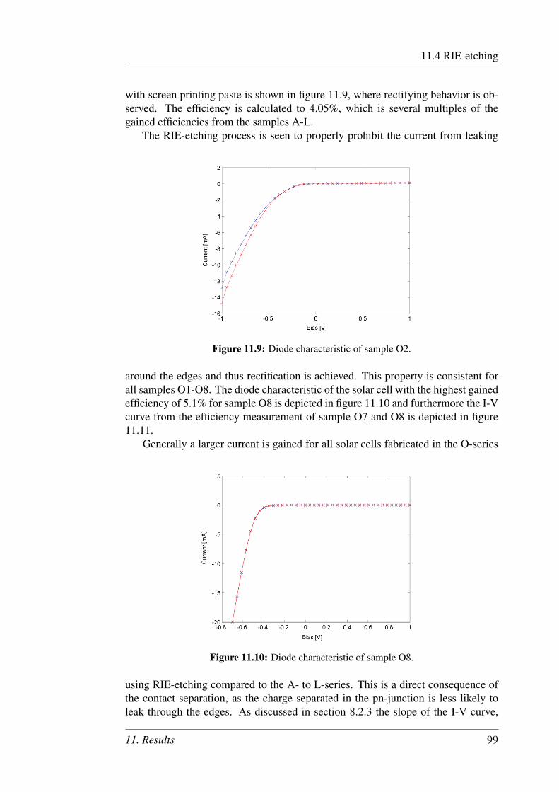
11.4 RIE-etching
with screen printing paste is shown in figure 11.9, where rectifying behavior is ob-served. The efficiency is calculated to 4.05%, which is several multiples of thegained efficiencies from the samples A-L.
The RIE-etching process is seen to properly prohibit the current from leaking
Figure 11.9: Diode characteristic of sample O2.
around the edges and thus rectification is achieved. This property is consistent forall samples O1-O8. The diode characteristic of the solar cell with the highest gainedefficiency of 5.1% for sample O8 is depicted in figure 11.10 and furthermore the I-Vcurve from the efficiency measurement of sample O7 and O8 is depicted in figure11.11.
Generally a larger current is gained for all solar cells fabricated in the O-series
Figure 11.10: Diode characteristic of sample O8.
using RIE-etching compared to the A- to L-series. This is a direct consequence ofthe contact separation, as the charge separated in the pn-junction is less likely toleak through the edges. As discussed in section 8.2.3 the slope of the I-V curve,
11. Results 99

11.4 RIE-etching
before the break towards open circuit voltage, in figure 11.11(b) is given from theshunt resistance. The shunt resistance of sample O8 is calculated to 299Ω and theseries resistance given by the slope of the curve towards open circuit voltage, is cal-culated to be 5.13Ω. The open circuit voltage was measured to 0.56V and the shortcircuit current to 46.6mA for sample O8.
The wafers fabricated using 15-20Ω.cm substrates show a general lower effi-
(a) Sample O7.
(b) Sample O8.
Figure 11.11: I-V characteristic of sample O7 and O8 for measurements obtainedby the use of an artificial light source resembling the solar spectrum.
ciency than of the solar cells fabricated using 1.8-4.5Ω.cm substrates. This can becorrelated with the fact that the concentration of free carriers in this substrate is ofa lower value and thus create a weaker build-in electric field within the pn-junctionthat would lower the separation of charge carriers generated.
Though a proper shunt resistance was obtained for sample O8, the series re-sistance is sought to be lowered to gain higher currents for voltages closer to the
100 11. Results
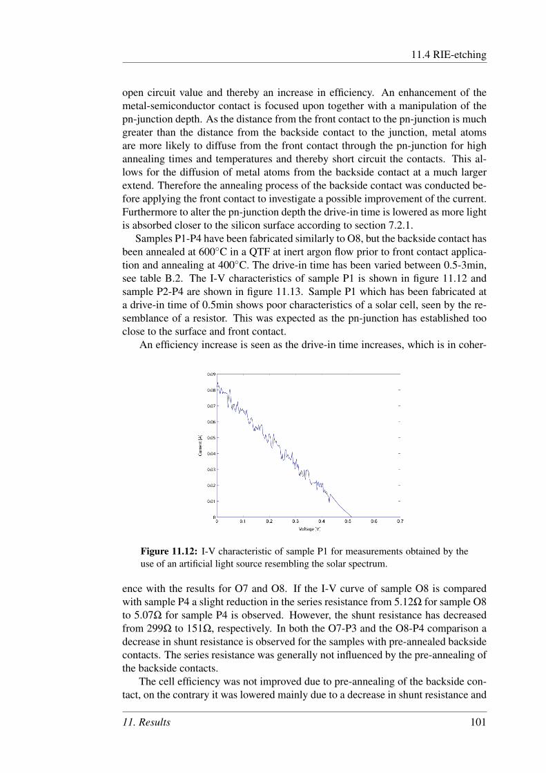
11.4 RIE-etching
open circuit value and thereby an increase in efficiency. An enhancement of themetal-semiconductor contact is focused upon together with a manipulation of thepn-junction depth. As the distance from the front contact to the pn-junction is muchgreater than the distance from the backside contact to the junction, metal atomsare more likely to diffuse from the front contact through the pn-junction for highannealing times and temperatures and thereby short circuit the contacts. This al-lows for the diffusion of metal atoms from the backside contact at a much largerextend. Therefore the annealing process of the backside contact was conducted be-fore applying the front contact to investigate a possible improvement of the current.Furthermore to alter the pn-junction depth the drive-in time is lowered as more lightis absorbed closer to the silicon surface according to section 7.2.1.
Samples P1-P4 have been fabricated similarly to O8, but the backside contact hasbeen annealed at 600C in a QTF at inert argon flow prior to front contact applica-tion and annealing at 400C. The drive-in time has been varied between 0.5-3min,see table B.2. The I-V characteristics of sample P1 is shown in figure 11.12 andsample P2-P4 are shown in figure 11.13. Sample P1 which has been fabricated ata drive-in time of 0.5min shows poor characteristics of a solar cell, seen by the re-semblance of a resistor. This was expected as the pn-junction has established tooclose to the surface and front contact.
An efficiency increase is seen as the drive-in time increases, which is in coher-
Figure 11.12: I-V characteristic of sample P1 for measurements obtained by theuse of an artificial light source resembling the solar spectrum.
ence with the results for O7 and O8. If the I-V curve of sample O8 is comparedwith sample P4 a slight reduction in the series resistance from 5.12Ω for sample O8to 5.07Ω for sample P4 is observed. However, the shunt resistance has decreasedfrom 299Ω to 151Ω, respectively. In both the O7-P3 and the O8-P4 comparison adecrease in shunt resistance is observed for the samples with pre-annealed backsidecontacts. The series resistance was generally not influenced by the pre-annealing ofthe backside contacts.
The cell efficiency was not improved due to pre-annealing of the backside con-tact, on the contrary it was lowered mainly due to a decrease in shunt resistance and
11. Results 101

11.4 RIE-etching
(a) Sample P2.
(b) Sample P3.
(c) Sample P4.
Figure 11.13: I-V characteristic of sample P2, P3, and P4 with increasing drive-intime, for measurements obtained by the use of an artificial light source resemblingthe solar spectrum.102 11. Results

11.4 RIE-etching
a lower short circuit current. A reason for this decrease in shunt resistance could bethat the annealing of the aluminum backside contact has allowed some aluminum todiffuse to the pn-interface at the surface allowing current to leak through the edgesdespite the physical distance of at least 1mm due to RIE-etching.
To examine the effect of annealing the front contact after backside contact an-nealing, the diode characteristics of sample P1-P4 were measured prior to and afterthe contact annealing at 400C. The diode characteristics prior to and after this an-nealing process is shown for sample P4 in figure 11.14. As expected the seriesresistance decreases after annealing, seen by comparing the slope of the I-V curves.This is in contrary to the fact that the isolated backside contact annealing did notexhibit this effect. As the backside contact annealing at 600C was conducted ina QTF, which has a low cool down rate, the inner tube containing the sample waspartly extracted from the QTF after the annealing time had expired, to not over ex-pose the contact. At this position of the inner tube, a flow of argon was still present,though decreased, compared to that prior to extraction. This could have allowed forair to access the sample building up a thin oxide layer. The measurement displayedin figure 11.14(a) is conducted with the front contact deposited onto this oxide thinfilm. The oxide thin film would have a degrading effect on the contact betweenmetal and semiconductor yielding a relatively high series resistance. However, asthe front contact is annealed, metal atoms will diffuse through the oxide thin filmand into the n-doped silicon establishing ohmic contact. This will decrease the se-ries resistance as seen in figure 11.14(b).
Basic polycrystalline silicon based solar cells with a total area efficiency of app.5% has been fabricated without the involvement of anti-reflecting coating. This isa resonable result considering that comercial high efficiency solar cells have a con-version efficiency of about 22%, as outlined in chapter 1. The RIE-etching processin the fabrication was found to have a significant effect on the shunt resistance ofthe solar cells fabricated. This was one of the key reasons that an efficiency of 5%was achieved and showed to be a reliable fabrication method. A decrease in thesolar cell series resistance was observed for solar cells with front contacts annealedat 400C for five minutes in a RTA. However, the isolated annealing of the backsidecontact, at 600C for five minutes in a QTF, did not exhibit the same positive effectas this resulted in a decrease in shunt resistance. Furthermore the thickness of phos-phorus screen printing paste was shown not to affect the measured sheet resistance,and thereby the phosphorus concentration and junction depth.
11. Results 103

11.4 RIE-etching
(a) Diode characteristic of sample P4 before contact annealing.
(b) Diode characteristic of sample P4 after contact annealing.
Figure 11.14: Diode characteristic of sample P4 before and after front and back-side contact annealing. A decrease in series resistance is observed after annealing.
104 11. Results
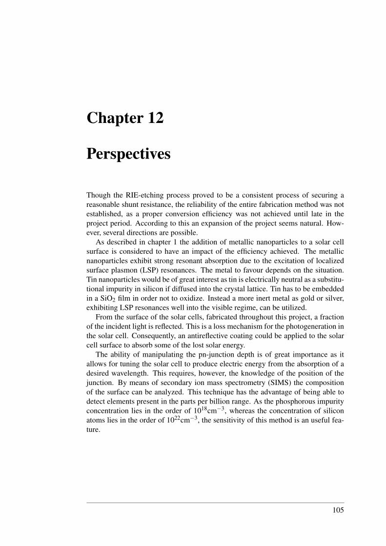
Chapter 12
Perspectives
Though the RIE-etching process proved to be a consistent process of securing areasonable shunt resistance, the reliability of the entire fabrication method was notestablished, as a proper conversion efficiency was not achieved until late in theproject period. According to this an expansion of the project seems natural. How-ever, several directions are possible.
As described in chapter 1 the addition of metallic nanoparticles to a solar cellsurface is considered to have an impact of the efficiency achieved. The metallicnanoparticles exhibit strong resonant absorption due to the excitation of localizedsurface plasmon (LSP) resonances. The metal to favour depends on the situation.Tin nanoparticles would be of great interest as tin is electrically neutral as a substitu-tional impurity in silicon if diffused into the crystal lattice. Tin has to be embeddedin a SiO2 film in order not to oxidize. Instead a more inert metal as gold or silver,exhibiting LSP resonances well into the visible regime, can be utilized.
From the surface of the solar cells, fabricated throughout this project, a fractionof the incident light is reflected. This is a loss mechanism for the photogeneration inthe solar cell. Consequently, an antireflective coating could be applied to the solarcell surface to absorb some of the lost solar energy.
The ability of manipulating the pn-junction depth is of great importance as itallows for tuning the solar cell to produce electric energy from the absorption of adesired wavelength. This requires, however, the knowledge of the position of thejunction. By means of secondary ion mass spectrometry (SIMS) the compositionof the surface can be analyzed. This technique has the advantage of being able todetect elements present in the parts per billion range. As the phosphorous impurityconcentration lies in the order of 1018cm−3, whereas the concentration of siliconatoms lies in the order of 1022cm−3, the sensitivity of this method is an useful fea-ture.
105

106 12. Perspectives
Chapter 13
Conclusion
The main motive of this thesis is to examine methods of fabricating functional solarcells and means for enhancing their efficiency due to the environmental demandingof greener energy sources such as that from solar cells, as briefly discussed in chap-ter 1. This lead to the initiating problem statement: "How can a basic solar cell withrectifying diode behavior be fabricated, and how can the specific characteristics ofthe solar cell be enhanced?" Thus, in order to create a pn-junction within a p-dopedsilicon substrate, phosphorus was used as n-type dopant. The fabricated solar cellswere characterized by measuring their sheet resistance, their diode behavior in thedark and under illumination, and their I-V characteristics when illuminated by anartificial sun. These characterization methods enabled the calculation of the effi-ciency for each individual cell fabricated.
Initially the dynamics of electron and holes plus the concept of impurities insemiconductor crystal lattices are described in chapter 3 to understand the conceptof diffusion of a dopant into a substrate in chapter 4. Furthermore, semiconductorstatistics are investigated to describe the pn-junction formation in a semiconductingmaterial in chapter 6 and the metal-semiconductor interface is described for alu-minum and silicon. Finally the transmittance of a range of wavelength has beencalculated in chapter 7 for silicon, to give an estimate of an optimum absorptiondepth of the material.
In the fabrication process two methods of applying phosphorus to the silicon sub-strate, for the formation of a pn-junction, were utilized. Phosphorus screen printingpaste was screen printed on using a mesh, shown in figure 9.3. Furthermore a spin-on phosphorus dopant was spun on the silicon substrates, and in addition, the screenprint phosphorus dopant was also used in the spin-on method. To enhance the cha-racteristics of the individual solar cells several means were taken into considerationto obtain rectifying diode behavior and to increase the photocurrent, this approachis described chronologically in the discussion in chapter 11.
Solar cells with rectifying diode behavior were obtained for both phosphorusdopants. The RIE-etching process, outlined in section 11.4, used to etch the sides ofthe solar cells was imperative to gain this behavior. A maximum efficiency of 5%was achieved for a fabricated polycrystallin silicon solar cell using spin-on phos-phorus as dopant, sample O8 in table B.2. Using screen printing phosphorus paste
107

a maximum efficiency was achieved at 4%. An open circuit voltage of 0.56V and ashort circuit current of 46.65mA were obtained for the solar cell with an efficiencyof 5%. The diode characteristic of sample O8 is shown in figure 11.10 and its I-Vcharacteristic is shown in figure 11.11(b).
Functional solar cells have been fabricated and by improving the fabricationmethods their efficiency has been increased. An efficiency of 5% is reasonable,as no antireflective coating has been utilized, and a high efficiency for commercialsolar cells lies at app. 22%.
To enhance the efficiency further of the fabricated solar cells anti reflective coat-ing could be placed on the surface to harness more of the incoming radiation. Thelocalized plasmon resonances of metallic nanoparticles could be utilized by intro-ducing it to the surface to enhance the solar cell efficiency via their strong resonantabsorption.
108 13. Conclusion

Bibliography
[1] M. Balkanski and R. F. Wallis. Semiconductor Physics and Applications. OX-FORD University Press, 2007.
[2] Stephen A. Campbell. Fabrication Engineering at the Micro- and Nanoscale.Oxford University Press, 2008.
[3] Mads Møgelmose Kjeldsen et al. Tuning the plasmon resonance of metallictin nanocrystals in si-based materials. Applied Physics A, 100(1):7, 2010.
[4] Thomas W. Krygowski et al. A novel processing technology for high-efficiency silicon solar cells. Journal of The Electrochemical Society, 1999.
[5] Inc. Filmetrics. Refractive index of silicon, si.
[6] Charles Kittel. Introduction to Solid State Physics 8th ed. John Wiley & Sons,Inc., 2005. ISBN 0-471-41526-X.
[7] Miles V. Klein and Thomas E. Furtak. Optics. John Wiley & Sons, 2 edition,1986. ISBN: 0-471-87297-0.
[8] Hans Lüth. Solid Surfaces, Interfaces and Thin Films. Springer, 5th ed. edi-tion, 2010.
[9] Jenny Nelson. The Physics of Solar Cells. Imperial College Press, 2003.
[10] Endeas Oy. Quick sun, photovoltaic measurement systems, 2010.
[11] Maria Berg Badstue Pedersen. Dansk solcelleforening: Husk potentialet isolceller, october 2010.
[12] Argonne National Laboratory Renée M. Nault. Basic research needs for so-lar energy utilization. Technical report, U.S. Department of Energy, 2005,September.
[13] Wikipedia. Kyoto protocol, 2011.
[14] Wikipedia. World energy consumption, 2011.
109

BIBLIOGRAPHY
110 BIBLIOGRAPHY
Appendix A
Electromagnetic Respons
As electromagnetic radiation interacts with either a solid, a liquid, or a gas the in-teraction is described using the terms of absorption, dispersion, and scattering. Theexposed material is perturbated by the incoming electromagnetic field and the pro-cess can involve either electronic states or vibrational states or both simultaneously.This can lead to transitions between states in the material e.g. an electron receivesenough energy to excite from valence to the conduction band, as in the case for semiconductors. If the transition rate is calculated it becomes possible to determine theoptical properties of consideration. This appendix presents a general formulation ofthe electromagnetic response of matter and lastly the response of a dielectric.[1, p.228]
A.1 Maxwell’s equations
The four well known equations describe the electrodynamics in the presence ofmatter and are formulated as follows;
~∇ ·~E =ρ
ε0
~∇×~E =−µ0∂~H∂t
(A.1)
~∇ · ~H =0 (A.2)
~∇× ~H =ε0∂~E∂t
+ ~J, (A.3)
where ~E is the electric field, ~H is the magnetic field, ρ is the electric charge density,and ~J is the electric current density. ε0 and µ0 are the permittivity and the perme-ability respectively. If the material is magnetic one writes equation (A.1) and (A.2)as
111

A.1 Maxwell’s equations
~∇×~E =− ∂~B∂t
~∇ ·~B =0,
where ~B is the magnetic induction. If the magnetization is introduced as ~M, mag-netic dipole moment per unit volume, and the magnetic permeability tensor µ, themagnetic induction can be expressed as
~B = µ0(~H + ~M) = µ0µ · ~H. (A.4)
In addition the magnetization and magnetic field are related through,
~M = χm · ~H, (A.5)
where χm is the magnetic susceptibility tensor. It can be deduced from equations(A.4) and (A.5) that µ = I + χm is true. For nonmagnetic materials, χm = 0 and~B = µ0~H.
In order to describe the interaction between the radiation field and an electricallypolarizable medium one introduces the polarization vector ~P, defined as the elec-trical dipole moment per unit volume, and the electrical displacement ~D, which isrelated to ~E and ~P through
~D = ε0~E +~P. (A.6)
When a crystal is pertubated by an electrical field ~E it becomes polarized due to anacquired electrical dipole moment, and in the linear limit, the response is
~P = ε0χ ·~E, (A.7)
where χ is the dielectric susceptibility tensor. If (A.7) is substituted into (A.6) thedisplacement vector becomes
~D = ε0(I +χ) ·~E.
The dielectric tensor is now introduced as ε by the relation
ε = I +χ,
Thus the displacement field can be written as
~D = ε0ε ·~E.
The dielectric tensor yields information about how the dielectric medium responseto the presence of an electromagnetic field.
More generally the above mentioned fields are functions of both time t and po-sition~r. In fact if the field quantities vary in time with a frequency ω the materialparameters χ, ε, and µ also in general are functions of ω. However for brevity, it isassumed that the response is local meaning that the fields are evaluated at the sameposition~r.
112 A. Electromagnetic Respons
A.1 Maxwell’s equations
A.1.1 Electromagnetic wave propagation in a conductive medium
The total electric current density, ~Jt of a conducting material is related to the electricfield ~E through
~Jt = σ~E,
assuming linear response due to the applied field. σ is here the complex electricalconductivity.
I order to find the total electric current two contributions are needed. Firstlythe steady state part due to motion of unbound charges and the latter due to themotion of time-dependent bound charges. The contribution from the bound part isthe time derivative of the polarization vector, ∂~P/∂t, and thus the sum from the twocontribution to the current density can be written as
~J = ~Jcond +∂~P∂t
. (A.8)
Here ~Jcond is the current contribution from the unbound charges and is given by~Jcond = σ~E.
If equation (A.8) is substituted into equation (A.3) and utilizing equation (A.6)this yields
~∇× ~H =∂~D∂t
+ ~Jcond = ~Jt . (A.9)
As a first approximation, when dealing with the optical properties of semiconduc-tors, the steady current ~Jcond from free carriers can be left out. Thus the time-dependent currents can be regarded only for simplicity. The current contributionthen becomes
~J =∂~P∂t
, (A.10)
and as a consequence the curl of ~H becomes
~∇× ~H =∂~D∂t
. (A.11)
In the following equation (A.11) is used instead of equations (A.3) and (A.9), thatis, ~Jcond is left out as an approximation.
To analyze an electrically neutral solid further another important property canbe calculated by taking the divergence of equation (A.6) and utilizing ~∇~E = ρ/ε0,hence
~∇ ·~D = ρ+~∇ ·~P. (A.12)
Now if equation (A.10) is substituted into the equation of continuity,
∂ρ
∂t+~∇ · ~J = 0,
A. Electromagnetic Respons 113

A.1 Maxwell’s equations
this yields
ρ =−~∇ ·~P. (A.13)
Conclusively equation (A.13) is substituted into (A.12) yielding
~∇ ·~D = 0. (A.14)
The derivation of the electrodynamic equations for an electrically neutral polariz-able material is thus completed with the approximation of neglecting the steadycontribution to the current, ~Jcond .
The dispersion relation for an electromagnetic wave propagating in a dielectricmedium is sought lastly in the following, assuming that the medium is nonmagnetic.Utilizing Maxwell’s equations the procedure is to take the curl of equation (A.1) anutilizing equation (A.11)
~∇×~∇×~E =~∇×−µ0∂~H∂t⇔
=−µ0∂
∂t
(~∇× ~H
)⇔
=−µ0∂2~D∂t2 (A.15)
For brevity a linear response in the medium due to the electric field is assumed, thus
~D = ε0ε~E, (A.16)
with ε being some scalar dielectric constant. Equation (A.15) can hence be rewrittenas
~∇×~∇×~E =− ε
c2∂2~D∂t2 , (A.17)
where c = (µ0ε0)−1 is the speed of light in vacuum. The double rotor of ~E is
rewritten using a vector identity and (A.17) becomes
~∇(~∇ ·~E−∇2~E) =− ε
c2∂2~D∂t2 . (A.18)
Utilizing equations (A.14) and (A.16) the expression in equation (A.18) reduces tothe well known wave equation
∇2~E =
ε
c2∂2~E∂t2 . (A.19)
To solve the wave equation a plane wave solution is sought of the form
~E(~r, t) = ~E0ei(~k·~r−ωt), (A.20)
where ~E0 is the amplitude of the electric field, ~k is the wave vector, and ω is thefrequency. Substituting (A.20) into equation (A.19) yields for a nontrivial solution:
114 A. Electromagnetic Respons
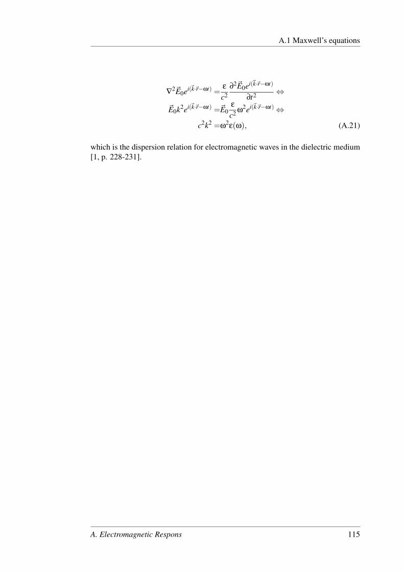
A.1 Maxwell’s equations
∇2~E0ei(~k·~r−ωt) =
ε
c2∂2~E0ei(~k·~r−ωt)
∂t2 ⇔
~E0k2ei(~k·~r−ωt) =~E0ε
c2 ω2ei(~k·~r−ωt)⇔
c2k2 =ω2ε(ω), (A.21)
which is the dispersion relation for electromagnetic waves in the dielectric medium[1, p. 228-231].
A. Electromagnetic Respons 115

A.1 Maxwell’s equations
116 A. Electromagnetic Respons

Appendix B
Specifics of Fabricated Solar Cells
Sample Phosphorous Drive-in HF Sheetres. EfficiencyA1 sosp 1k RPM Carb. 950C/1.5min 1%/0.5minA2 sosp 1k RPM Carb. 950C/3min 1%/0.5minA3 sosp 2k RPM Carb. 950C/1.5min 1%/0.5minA4 sosp 2k RPM Carb. 950C/3min 1%/0.5minB1 sp Carb. 950C/1.5min 1%/0.5minB2 sp Carb. 950C/3min 1%/0.5minB3 sp Carb. 950C/1.5min 1%/0.5minB4 sp Carb. 950C/3min 1%/0.5minC1 sp QTF 1000C/1.5min* 10%/2min 0.045%C2 sp QTF 1000C/3min* 10%/2min 0.024%D sp QTF 1000C/3min* 10%/2min 44.01Ω/sq 0.37%E ErrorF1 ErrorF2 ErrorG1 sp QTF 1000C/3min* 10%/2min 17.4Ω/sq 0.092%G2 sp QTF 1000C/5min* 10%/2min 13.55Ω/sq 0.23%G3 sp QTF 1000C/7min* 10%/2min 12.7Ω/sq 0.144%G4 sp QTF 1000C/9min* 10%/2min 11.24Ω/sq 0.197%H1 sp QTF 1000C/1min 10%/2min 20.53Ω/sq 0.177%H2 sp QTF 1000C/3min 10%/2min 12.1Ω/sq 0.179%H3 sp QTF 1000C/5min 10%/2min 9.6Ω/sq 0.21%I sp QTF 1000C/3min 10%/2min 13.64Ω/sq 0.33%
Table B.1: Specifications for each single solar cell fabricated. sp: screen print, so:spin-on, sosp: spin-on using phosphorus screen-printing paste, RTA: Rapid Ther-mal Annealer, QTF: Quartz Tube Furnace. All samples fabricated with phosphorusscreen-printing paste have been heated on a hot plate for 15 minutes at 150C afterphosphorus application. Samples fabricated with spin-on phosphorus have beenheated for one minute at 200C. (*) The drive-in temperature of the samples wasnot 1000C, as the inner tube was not preheated with the main tube.
117

Sample Phosphorous Annealing HF Sheetres. EfficiencyJ1 so-5k rmp QTF 1000C/3min 10%/2min 27.55Ω/sq 0.59%J2 sp QTF 1000C/3min 10%/2min 17.9Ω/sq 0.4%K1 sp QTF 1050C/2min 10%/2min 10.7Ω/sq 0.2%K2 sp QTF 1050C/4min 10%/2min 7.75Ω/sq 0.09%K3 sp QTF 1050C/6min 10%/2min 6.3Ω/sq 0.09%L1 sp QTF 1000C/3min 10%/2min 18.76Ω/sq 0.13%L2 sp QTF 1000C/5min 10%/2min 16.63Ω/sq 0.17%M1 sosp-2k rmp QTF 1000C/1.5min 10%/2min 21.48Ω/sq 0.23%M2 sosp-2k rmp QTF 1000C/3min 10%/2min 14.9Ω/sq 0.34%N1 sosp-2k rmp QTF 1000C/1.5min 10%/2min 24.25Ω/sq 0.8%N2 sosp-2k rmp QTF 1000C/3min 10%/2min 15.86Ω/sq 2.42%O1 sosp-2k rmp QTF 1000C/2min 10%/2min 18.9Ω/sq 1.98%O2 sosp-2k rmp QTF 1000C/3min 10%/2min 15.5Ω/sq 4.05%
O3** sosp-2k rmp QTF 1000C/2min 10%/2min 19.94Ω/sq 0.18%O4** sosp-2k rmp QTF 1000C/3min 10%/2min 15.9Ω/sq 0.52%O5** so-2k rmp QTF 1000C/2min 10%/2min 22.8Ω/sq 0.60%O6** so-2k rmp QTF 1000C/3min 10%/2min 20.44Ω/sq 2.52%O7 so-2k rmp QTF 1000C/2min 10%/2min 19.58Ω/sq 3.88%O8 so-2k rmp QTF 1000C/3min 10%/2min 24.56Ω/sq 5.1%
P1*** so-2k rmp QTF 1000C/0.5min 10%/2min 434.98Ω/sq 0.43%P2*** so-2k rmp QTF 1000C/1min 10%/2min 39.84Ω/sq 3.62%P3*** so-2k rmp QTF 1000C/2min 10%/2min 21.71Ω/sq 4.01%P4*** so-2k rmp QTF 1000C/3min 10%/2min 16.41Ω/sq 4.65%
Table B.2: Specifications for each single solar cell fabricated. sp: screen print, so:spin-on, sosp: spin-on using phosphorus screen-printing paste, RTA: Rapid Ther-mal Annealer, QTF: Quartz Tube Furnace. All samples fabricated with phosphorusscreen-printing paste have been heated on a hot plate for 15 minutes at 150C afterphosphorus application. Samples fabricated with spin-on phosphorus have beenheated for one minute at 200C. (**) Substrate of resistivity at 15-20Omega/sqwas utilized. (***) Backside contact has been annealed at 600C for 5min prior tofront contact application.
118 B. Specifics of Fabricated Solar Cells


