IEEE TRANSACTIONS ON ELECTRON DEVICES, VOL. 49, NO. 12, DECEMBER 2002 2323
Fabrication and Characterization ofPolycrystalline SiC Resonators
Shuvo Roy, Member, IEEE, Russell G. DeAnna, Christian A. Zorman, Member, IEEE, andMehran Mehregany, Senior Member, IEEE
Abstract—This paper presents the development of polycrys-talline 3C silicon carbide (polySiC) lateral resonant devices, whichare fabricated by a three-mask surface micromachining processusing silicon dioxide (SiO2), polysilicon, and nickel (Ni) as theisolation, sacrificial, and contact metallization layers, respectively.The polySiC resonators are packaged for operation in hightemperature environments using ceramic-based materials andnickel wirebonding procedures. Device operation is successfullydemonstrated over 10 5–760 torr and 22–950 C pressureand temperature ranges, respectively. Quality factors ( s) of
100 000 at 10 5 torr and resonant frequency drifts of 18ppm/h under continuous operation are achieved using an scanningelectron microscope (SEM) setup. Device resonant frequencyvaries nonlinearly with increasing operating temperature. Finiteelement modeling reveals that this variation resulted from theinterplay between the Young’s modulus of polySiC and inducedstresses, which occur due to mismatch in thermal expansioncoefficients of the polySiC film and the underlying silicon (Si)substrate.
Index Terms—High temperature transducers, lateral resonantdevices, microelectromechanical systems (MEMS), microsystems,polySiC, resonators, silicon carbide (SiC), surface microma-chining.
I. INTRODUCTION
M ICROMACHINED polysilicon resonators are emergingas potential on-chip replacements for conventional
discrete oscillators and filters in high performance communi-cation transceivers [1]. The integrated microelectromechanicalpolysilicon devices exhibit frequency selectivity characteristicsthat are superior to integrated active filtering techniquesbased upon traditional electron devices. Micromachined res-onator s of 80 000 under vacuum conditions and resonantfrequency coefficients of 10 ppm/ C have been reported[2]. In addition to high transceiver components, the utilityof polysilicon resonators has also been demonstrated in anumber of other applications including mechanical properties
Manuscript received May 30, 2002; revised October 14, 2002. This work wassupported by DARPA MTO under Grant DABT63-98-1-0010 and ARO/MURIunder Grant DAAH04-95-10097. The review of this paper was arranged byEditor K. Najafi.
S. Roy is with the Department of Biomedical Engineering, The ClevelandClinic Foundation, Cleveland, OH 44195 USA (e-mail: [email protected]).
R. DeAnna was with the U.S. Army Research Laboratory, Vehicle Tech-nology Center, NASA Glenn Research Center at Lewis Field, Cleveland, OH44135 USA. He is now with Advanced Engineering Technologies, Norcross,GA 30071 USA.
C. Zorman and M. Mehregany are with the Department of Electrical Engi-neering and Computer Science, Case Western Reserve University, Cleveland,OH 44106 USA.
Digital Object Identifier 10.1109/TED.2002.807445
testing, pressure sensing, and inertial navigation systems[3]–[5]. However, the electrical and mechanical properties ofpolysilicon begin to rapidly degrade at elevated temperatures( 350 C), making it increasingly unsuitable for high temper-ature applications [6]–[8]. In contrast, SiC is well known for itsmechanical characteristics, such as high Young’s modulus andyield strength, chemical inertness, high thermal conductivity,and electrical stability at temperatures well above 600C [8],[9]. Although these material properties and microfabricationcompatibility of SiC make it an attractive structural materialfor fabrication of high and/or high temperature microelec-tromechanical devices, the development of SiC as a structuralmaterial has been limited by a combination of fabrication,packaging, and testing challenges.
The lack of a durable wire bonding technology is a major im-pediment to the implementation of SiC-based devices for hightemperature applications. We have developed a nickel (Ni) wirebonding process for Ni contact pads on 3C-SiC films using con-ventional tools and wire diameters and demonstrated reliableoperation up to 550C [10]. Ni is attractive as a contact metalfor high temperature SiC devices in that Ni has a melting tem-perature of 1453C, forms an ohmic contact to both n-type andp-type 3C-SiC substrates, and is also available in wire diameterssimilar to that of the Al and Au bonding wires (e.g., 25m).For high temperature applications, it is desired that the contactpad and the wire be of the same material because intermetallicgrowth and interface corrosion, which can occur between dis-similar metals at high temperatures, results in a rapid degrada-tion of bond strength and a shift in the principal failure modefrom wire breaks to bond lifts. The stability of the wire bondsis threatened by such a problem, especially at elevated tempera-tures. Therefore, reliability should be improved when pad met-allization and bonding wires are of the same material.
This paper presents the development of polycrystallineSiC (polySiC) folded beam lateral resonant devices (subse-quently called resonators) that are fabricated, packaged, andsuccessfully operated over a wide range of pressures andtemperatures. First, the fabrication of polySiC resonators by asurface micromachining process using silicon dioxide (SiO),polysilicon, and Ni as the isolation, sacrificial, and contactmetallization layers, respectively, is presented. Details of theresonator packaging scheme using ceramic-based materials andNi wirebonding procedures are then outlined. Next, testing pro-cedures and optical and scanning electron microscope-basedexperimental setups to investigate changes in resonatorwith pressure and resonant frequency with temperature aredescribed. Finally, resonator testing results at both room and
2324 IEEE TRANSACTIONS ON ELECTRON DEVICES, VOL. 49, NO. 12, DECEMBER 2002
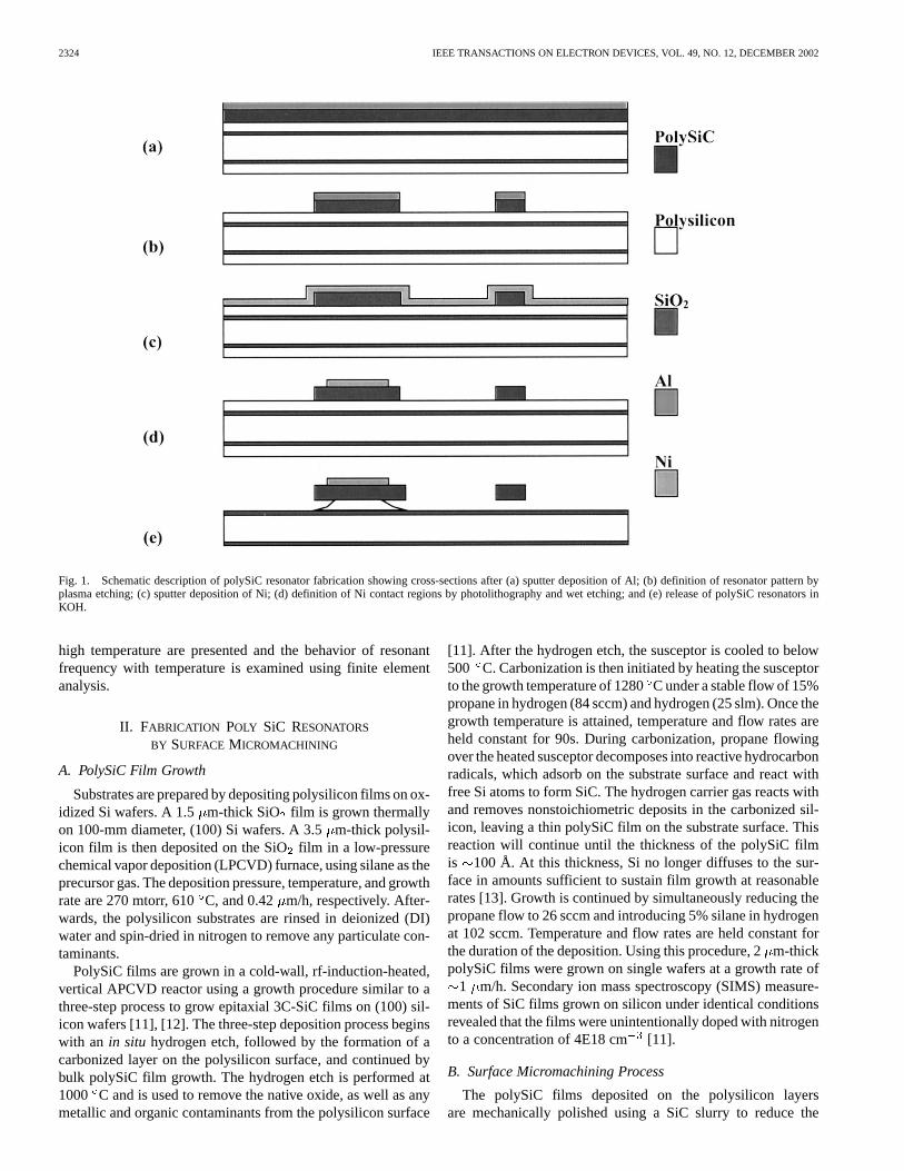
Fig. 1. Schematic description of polySiC resonator fabrication showing cross-sections after (a) sputter deposition of Al; (b) definition of resonator pattern byplasma etching; (c) sputter deposition of Ni; (d) definition of Ni contact regions by photolithography and wet etching; and (e) release of polySiC resonators inKOH.
high temperature are presented and the behavior of resonantfrequency with temperature is examined using finite elementanalysis.
II. FABRICATION POLY SiC RESONATORS
BY SURFACE MICROMACHINING
A. PolySiC Film Growth
Substrates are prepared by depositing polysilicon films on ox-idized Si wafers. A 1.5 m-thick SiO film is grown thermallyon 100-mm diameter, (100) Si wafers. A 3.5m-thick polysil-icon film is then deposited on the SiOfilm in a low-pressurechemical vapor deposition (LPCVD) furnace, using silane as theprecursor gas. The deposition pressure, temperature, and growthrate are 270 mtorr, 610C, and 0.42 m/h, respectively. After-wards, the polysilicon substrates are rinsed in deionized (DI)water and spin-dried in nitrogen to remove any particulate con-taminants.
PolySiC films are grown in a cold-wall, rf-induction-heated,vertical APCVD reactor using a growth procedure similar to athree-step process to grow epitaxial 3C-SiC films on (100) sil-icon wafers [11], [12]. The three-step deposition process beginswith an in situ hydrogen etch, followed by the formation of acarbonized layer on the polysilicon surface, and continued bybulk polySiC film growth. The hydrogen etch is performed at1000 C and is used to remove the native oxide, as well as anymetallic and organic contaminants from the polysilicon surface
[11]. After the hydrogen etch, the susceptor is cooled to below500 C. Carbonization is then initiated by heating the susceptorto the growth temperature of 1280C under a stable flow of 15%propane in hydrogen (84 sccm) and hydrogen (25 slm). Once thegrowth temperature is attained, temperature and flow rates areheld constant for 90s. During carbonization, propane flowingover the heated susceptor decomposes into reactive hydrocarbonradicals, which adsorb on the substrate surface and react withfree Si atoms to form SiC. The hydrogen carrier gas reacts withand removes nonstoichiometric deposits in the carbonized sil-icon, leaving a thin polySiC film on the substrate surface. Thisreaction will continue until the thickness of the polySiC filmis 100 Å. At this thickness, Si no longer diffuses to the sur-face in amounts sufficient to sustain film growth at reasonablerates [13]. Growth is continued by simultaneously reducing thepropane flow to 26 sccm and introducing 5% silane in hydrogenat 102 sccm. Temperature and flow rates are held constant forthe duration of the deposition. Using this procedure, 2m-thickpolySiC films were grown on single wafers at a growth rate of
1 m/h. Secondary ion mass spectroscopy (SIMS) measure-ments of SiC films grown on silicon under identical conditionsrevealed that the films were unintentionally doped with nitrogento a concentration of 4E18 cm [11].
B. Surface Micromachining Process
The polySiC films deposited on the polysilicon layersare mechanically polished using a SiC slurry to reduce the
ROY et al.: FABRICATION AND CHARACTERIZATION OF POLYCRYSTALLINE SiC RESONATORS 2325
Fig. 2. SEM micrograph of a released polySiC lateral resonant device.The suspension beam lengths and widths are nominally 100�m and 2.5�m, respectively. Exposed polySiC shows up as dark gray, while the Nimetallization appears light gray.
surface roughness (Ra) from400 Å on the as-grown films to40 Å [14]. The polishing process results in a final polySiC
film thickness of 1.75 m. Fig. 1 outlines the fabrication ofpolySiC resonators by surface micromachining. A 5000 Å-thickaluminum (Al) film is deposited on the polished polySiC filmsby sputtering and subsequently patterned using photolithog-raphy and aluminum (Al) etchant to delineate the resonatorgeometry. Next, the resonator pattern is defined in the polySiCby dry etching in a CHF/O /He plasma with the patterned Alacting as etch mask [15]. Afterwards, the Al mask is strippedand a 7500 Å-thick Ni film is sputter deposited, patterned byphotolithography, and wet etched using commercial Ni etchantto define nickel contacts to the polySiC. Finally, the resonatoris released by a timed etch of the sacrificial polysilicon in40 wt.% KOH at 40 C and dried using a supercritical COdrying process. Fig. 2 presents a SEM micrograph of a releasedpolySiC resonator.
PolySiC resonators are fabricated on three different sub-strates (i.e., three separate polySiC growth runs), termedA, B,andC. After release and supercritical drying, but prior to pack-aging, all devices are examined under an optical microscope forpossible fabrication flaws and/or damage from handling. Res-onators are also manually probed using a micromanipulator tocheck for stiction. Flaw-, damage-, and stiction-free resonatorsare then examined using SEM to confirm structural integrityand measure resonator geometry. Using this procedure, 5resonators from each substrate are selected for packaging andtesting. These 15 resonators are subsequently termedA1–5,B1–5, andC1–5, where the letter identifies the substrate andthe numeral indicates the particular device.
III. PACKAGING OF POLY SiC RESONATORS
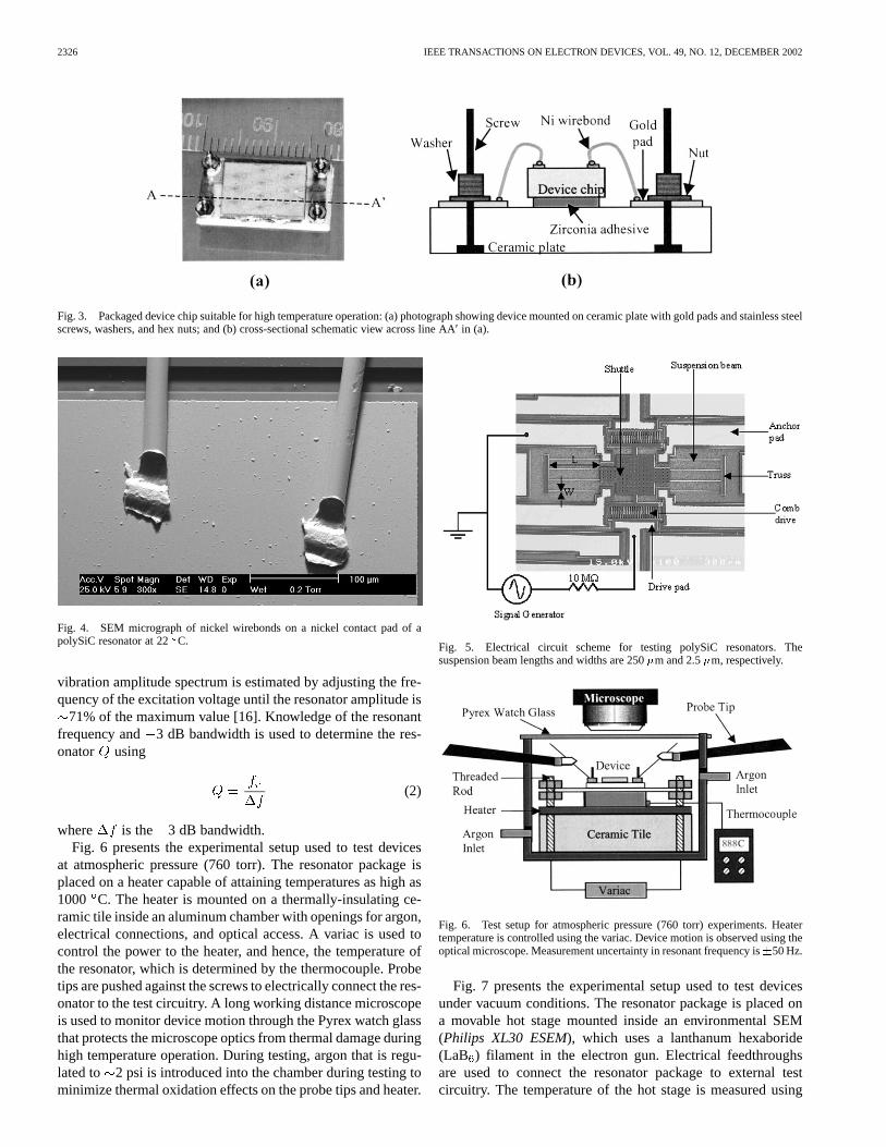
The released resonator chip is packaged for high temperatureoperation onto a ceramic plate with patterned gold pads andsteel posts as shown in Fig. 3. The chip is attached to theceramic plate using commercially available zirconia cement
(AREMCO Ultra-Temp 516), which is thermally conductive,stable to 1760 C, and resistant to chemical attack. The goldpads on the ceramic plate enable electrical connections fromthe resonator package to external circuitry through the stainlesssteel screws, nuts, and washers. Electrical connections from theNi contact pads on the resonator chip to the gold pads on theceramic plate are realized by 25m-diameter Ni wires, whichare attached by a thermosonic wirebonding process optimizedfor maximum pull strength [10]. In a typical thermosonic wire-bonding procedure, the resonator package is first mounted on astage and heated to 250C. The Ni bonding wire is then guidedto the first bonding site on a Ni contact pad of the polySiCresonator and pressed onto the surface with a force of340mN by a titanium carbide (TiC) wedge mounted on aKulicke& Soffa 4123ultrasonic wire bonder. While the wire is firmlyclamped between the contact pad and TiC wedge, a12 mspulse of 520 mW ultrasonic vibration is applied to the wedge.The ultrasonic energy causes localized wire deformation thatbreaks up the surface oxides at the bonding site, resultingin cold weld between the wire and contact metallization asshown in Fig. 4. Afterwards, the wedge, along with the wire,is lifted and positioned at a second bonding site on the goldpad on the ceramic plate and bonded similarly, forming a wireloop anchored at the nickel and gold pads. The wire clampsthen retract, pulling the wire and severing it near the end ofthe second bond. The wirebonding procedure is repeated toconnect other contact pads of the resonator to correspondinggold pads on the ceramic plate.
IV. TESTING PROCEDURES
The packaged resonators are tested under different pressureand temperature conditions. Fig. 5 presents the electrical cir-cuit scheme for resonator testing. A signal generator consistingof a HP 33 210Avariable function generator connected to aKrohn-Hite 7602Mwide-band power amplifier is used to applya 0–200 Vpp sinusoidal excitation voltage to the comb drive ofthe resonator. The polySiC shuttle and silicon substrate are bothelectrically grounded during testing and a high value series re-sistance (10 M ) is incorporated to provide short circuit pro-tection. Resonance is determined visually by adjusting the ex-citation voltage frequency applied from the signal generator tothe drive pad of the resonator until maximum resonator ampli-tude is observed. The application of a pure sinusoidal signal tothe comb drive leads to a frequency doubling effect, and con-sequently, the resonant frequency is twice the frequency of theexcitation voltage at which maximum resonator amplitude is ob-served [16]. The resonant frequency is related to device geom-etry and material properties according to [17]:
(1)
where is the resonant frequency, is the Young’s modulusof polySiC, is the film thickness, is the suspension beamwidth, is the suspension beam length, is the shuttle mass,
is the mass of the folding trusses, and is the total massof the suspension beams. The3 dB bandwidth of the resonator
2326 IEEE TRANSACTIONS ON ELECTRON DEVICES, VOL. 49, NO. 12, DECEMBER 2002
Fig. 3. Packaged device chip suitable for high temperature operation: (a) photograph showing device mounted on ceramic plate with gold pads and stainless steelscrews, washers, and hex nuts; and (b) cross-sectional schematic view across line AA′ in (a).
Fig. 4. SEM micrograph of nickel wirebonds on a nickel contact pad of apolySiC resonator at 22C.
vibration amplitude spectrum is estimated by adjusting the fre-quency of the excitation voltage until the resonator amplitude is
71% of the maximum value [16]. Knowledge of the resonantfrequency and 3 dB bandwidth is used to determine the res-onator using
(2)
where is the 3 dB bandwidth.Fig. 6 presents the experimental setup used to test devices
at atmospheric pressure (760 torr). The resonator package isplaced on a heater capable of attaining temperatures as high as1000 C. The heater is mounted on a thermally-insulating ce-ramic tile inside an aluminum chamber with openings for argon,electrical connections, and optical access. A variac is used tocontrol the power to the heater, and hence, the temperature ofthe resonator, which is determined by the thermocouple. Probetips are pushed against the screws to electrically connect the res-onator to the test circuitry. A long working distance microscopeis used to monitor device motion through the Pyrex watch glassthat protects the microscope optics from thermal damage duringhigh temperature operation. During testing, argon that is regu-lated to 2 psi is introduced into the chamber during testing tominimize thermal oxidation effects on the probe tips and heater.
Fig. 5. Electrical circuit scheme for testing polySiC resonators. Thesuspension beam lengths and widths are 250�m and 2.5�m, respectively.
Fig. 6. Test setup for atmospheric pressure (760 torr) experiments. Heatertemperature is controlled using the variac. Device motion is observed using theoptical microscope. Measurement uncertainty in resonant frequency is�50 Hz.
Fig. 7 presents the experimental setup used to test devicesunder vacuum conditions. The resonator package is placed ona movable hot stage mounted inside an environmental SEM(Philips XL30 ESEM), which uses a lanthanum hexaboride(LaB ) filament in the electron gun. Electrical feedthroughsare used to connect the resonator package to external testcircuitry. The temperature of the hot stage is measured using
ROY et al.: FABRICATION AND CHARACTERIZATION OF POLYCRYSTALLINE SiC RESONATORS 2327
Fig. 7. Schematic description of the environmental SEM setup used forexperiments under vacuum conditions. Device motion is observed on anattached monitor. Electrical feedthroughs are used to connect components toexternal circuitry. Measurement uncertainty in resonant frequency is<�1 Hz.
a thermocouple and resonator motion is observed using avideo monitor attached to the electron microscope optics. Inaddition to the room-temperature imaging capabilities of astandard SEM under high vacuum (chamber base pressure of2.6 10 torr) conditions, the environmental SEM can alsoperform imaging under low vacuum (0.1–20 torr) and/or hightemperature ( 1000 C) conditions.
V. RESULTS
A. Room Temperature Testing
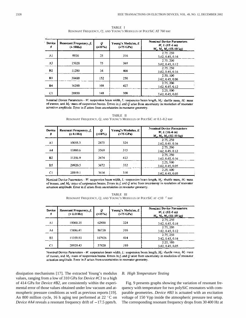
PolySiC resonators are tested using both the atmospheric andenvironmental SEM setups at room temperature. Young’s mod-ulus values are determined using (1) with experimentally-de-termined resonant frequencies, measured geometries of the res-onators, and assumed polySiC density of 3230 kg/mto cal-culate the mass of the shuttle, trusses, and beams [18]. Res-onator s are determined using (2) with the experimentally-de-termined 3 dB bandwidths. The wire bonds on seven of the15 packaged polySiC resonators broke due to handling mishapsduring testing, and consequently, only three devices (A1, B2,andC1) are characterized under all pressure conditions.
Table I presents a summary of resonators and extractedYoung’s modulus values of polySiC films using the atmosphericpressure setup at room temperature (22C). Resonant frequen-cies and 3 dB bandwidths of the resonators are determinedby applying excitation voltages of 40–170 Vpp, depending onspecific device geometry, which provided a vibration amplitudeof 5 m at resonance. The extracted Young’s modulus valuesrange from a low of 250 GPa forDevice #B3to a high of 427GPa forDevice #B4. The variation in the extracted Young’smodulus values can be attributed to errors in measurement ofresonator geometry and unintended fluctuations in growth con-ditions in the APCVD furnace during polySiC film growth. Nev-ertheless, the Young’s modulus are generally consistent withthe results of a preliminary study reported previously [19]. Res-onator s range from a low of 25 forDevice #A1to a high of
152 forDevice #B3. Examination of the data does not reveal anyreadily observable relationship between the extracted Young’smodulus values and resonators. However, there is a generalpositive correlation between resonatorand the resonant fre-quency: devices with higher resonant frequencies exhibit higher
s than lower resonant frequency devices. In the atmosphericpressure test setup, damping resulting from Couette flow under-neath the shuttle is the dominant energy dissipation mechanism,and consequently, the resonatoris proportional to stiffness ofthe resonator suspension [16]. Therefore, resonators with highersuspension stiffness, and hence, higher resonant frequencies,exhibit higher s than lower resonant frequency devices.
Table II presents a summary of resonators and extractedYoung’s modulus values of polySiC determined using theenvironmental SEM test setup at room temperature under lowvacuum conditions (0.1–0.2 torr). Exact pressure control in theSEM is not possible under the low vacuum conditions and pres-sure determination is difficult since the pressure gauge readingsare not reliable near the base pressure of the mechanical pump,which is approximately 0.1–0.2 torr. Resonant frequencies and
3 dB bandwidths of the resonators are determined by applyingexcitation voltages of 2–10 Vpp, depending on specific devicegeometry, which provided a vibration amplitude of5 mat resonance. Resonators and Young’s modulus values aredetermined in a manner similar to those for the atmosphericpressure testing described earlier. Resonators at low vacuumare significantly larger than resonators determined underatmospheric pressure conditions due to decreased damping ef-fects at 0.1–0.2 torr. However, Couette flow is still the dominantenergy dissipation mechanism under low vacuum conditionssince resonator s increase with resonant frequency from alow 2875 forDevice #A1(10 055.3 Hz resonant frequency) to ahigh of 3672 forDevice #B5(29 920.5 Hz resonant frequency).The extracted Young’s modulus values ranging from a low of310 GPa forDevice #C1to a high of 413 GPa forDevice #B2are consistently within the experimental error of those valuesobtained using the atmospheric pressure test setup as well asprevious reports [19].
Table III presents a summary of resonators and extractedYoung’s modulus values of polySiC determined using the en-vironmental SEM test setup at room temperature under highvacuum conditions ( torr). Although chamber pressuresas low as 2.6 10 torr are attainable, most determinationsof resonant frequencies and3 dB bandwidths are conductedat 5–9 10 torr. Fig. 8 presents a SEM micrograph of theshuttle section of an actuating resonator at9 10 torr. Res-onators required excitation voltages of 0.3–0.8 Vpp, dependingon specific device geometry, which provided amplitudes of atleast 5 m at resonance. Resonators and Young’s modulusvalues are determined in a manner similar to those describedfor the low vacuum testing earlier. Resonators at high vacuumare significantly larger than s determined under low vacuumconditions, ranging from a low of 57 828 forDevice #C1to ahigh of 107 926 forDevice #B2. In contrast to resonator sexhibited under atmospheric pressure and low vacuum condi-tions, s at high vacuum are not necessarily greater for higherresonant frequency devices since thermoelastic friction and an-chor losses, not Couette flow damping, are the primary energy
2328 IEEE TRANSACTIONS ON ELECTRON DEVICES, VOL. 49, NO. 12, DECEMBER 2002
TABLE IRESONANT FREQUENCY,Q, AND YOUNG’S MODULUS OFPOLYSiC AT 760 torr
TABLE IIRESONANT FREQUENCY, Q, AND YOUNG’S MODULUS OFPOLYSiC AT 0.1–0.2 torr
TABLE IIIRESONANT FREQUENCY,Q, AND YOUNG’S MODULUS OFPOLYSiC AT <10 torr
dissipation mechanisms [17]. The extracted Young’s modulusvalues, ranging from a low of 310 GPa forDevice #C1to a highof 414 GPa forDevice #B2, are consistently within the experi-mental error of those values obtained under low vacuum and at-mospheric pressure conditions as well as previous reports [19].An 800 million cycle, 16 h aging test performed at 22C onDevice #A4reveals a resonant frequency drift of17.5 ppm/h.
B. High Temperature Testing
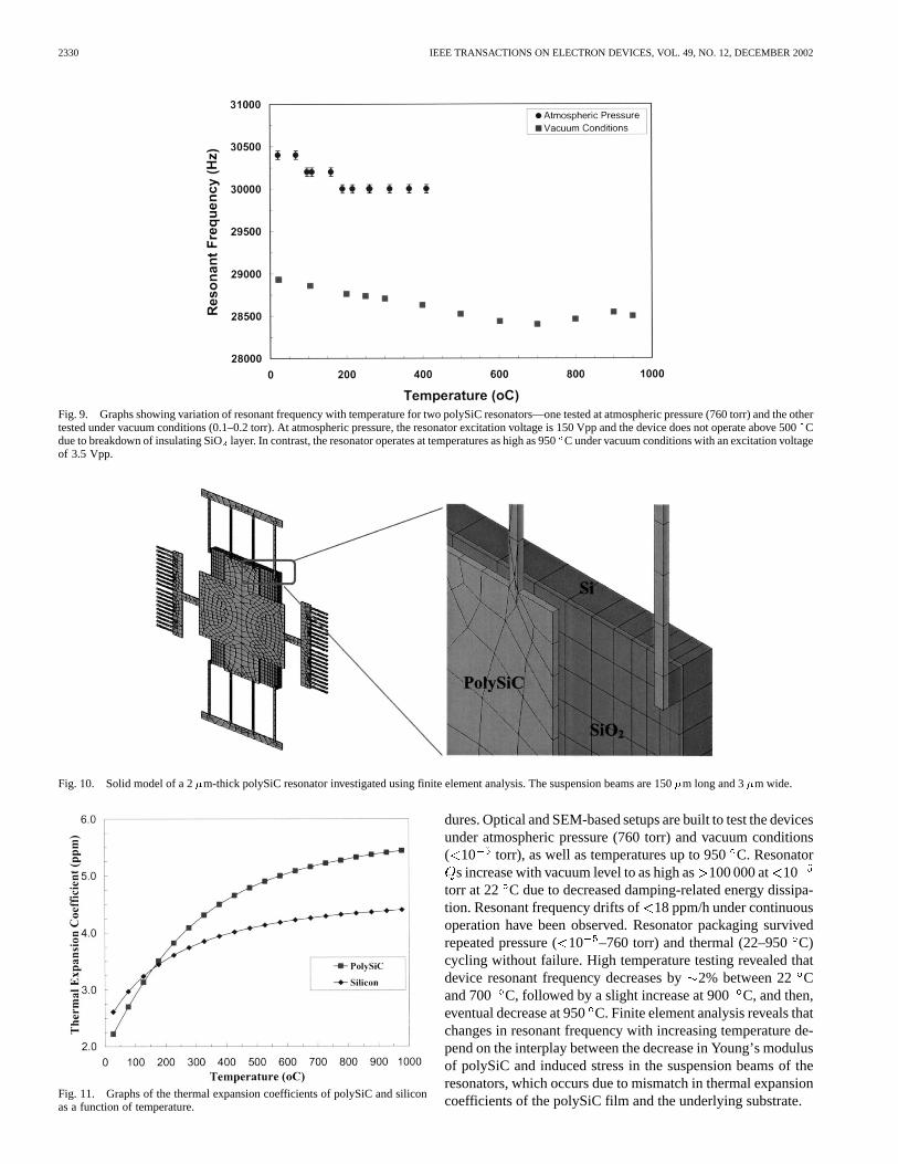
Fig. 9 presents graphs showing the variation of resonant fre-quency with temperature for two polySiC resonators with com-parable geometries.Device #B3is actuated with an excitationvoltage of 150 Vpp inside the atmospheric pressure test setup.The corresponding resonant frequency drops from 30 400 Hz at
ROY et al.: FABRICATION AND CHARACTERIZATION OF POLYCRYSTALLINE SiC RESONATORS 2329
Fig. 8. SEM micrograph of shuttle section near a comb drive of a polySiCresonator under actuation at 9� 10 torr and 22 C. Frequency of theexcitation voltage is 10 059.94 Hz. The distance between blur edges is theresonator amplitude.
22 C to 30 000 Hz at 410C. Resonator actuation is not ob-served above 500C in the atmospheric pressure setup. How-ever, upon cooling to temperatures below 500C, resonatoroperation resumes, which suggests the possibility of dielectricbreakdown of the electrically isolating SiOlayer above 500C.Device #C1is actuated with an excitation voltage of 3.5 Vppunder low vacuum (0.1–0.2 torr) conditions. The resonator op-erates over a 22–950C temperature range. In contrast to deviceoperation in the atmospheric pressure setup, the lower excitationvoltage used to resonate the polySiC actuators under vacuumconditions ensures that electrically isolating SiOlayer does notexhibit dielectric breakdown at elevated temperatures. The reso-nant frequency of the vacuum-tested device drops steadily from28 930 Hz at 22 C to 28 402 Hz at 700C, followed by anincrease to 28 544 Hz at 900C, and then a slight decrease to28 500 at 950C. Resonator actuation at temperatures950 Cis not attempted due to concerns about the lifetime of the LaBfilament in the electron gun of the environmental SEM.
The resonator package survives repeated pressure( 10 –760 torr) and thermal (22–950C) cycling withoutfailure. Nickel wirebonds on resonator contact pads were exam-ined in the SEM during high temperature operation at 500Cand after cooling down to room temperature from 950C. Thewirebonds do not exhibit any observable degradation due to thethermal cycling or high temperature.
Finite element analysis is performed to investigate changes inresonant frequency with increasing temperature. A preliminaryfinite element model is analyzed using ANSYS5.3 software toexamine interactions between the polySiC resonator and under-lying silicon substrate [20]. Fig. 10 presents the model of a 2
m thick resonator with 150m long and 3 m wide suspen-sion beams anchored on a 3.5m thick polysilicon layer over-lying a 1.5 m thick SiO film on the silicon substrate, which isa typical geometric construction of devices tested. The polySiClayer is meshed with 20-node brick elements, while underlyinglayers are meshed with eight-node brick elements. The bottomof the silicon substrate is fixed in the direction normal to the sur-face and allowed free thermal expansion in directions parallel
to the surface. Fig. 11 presents a graph showing the variation ofthermal expansion coefficients with temperature for 3C-SiC (as-sumed equivalent to polySiC) and silicon, while Table IV liststhe other material properties used in the finite element analysis[20]–[22].
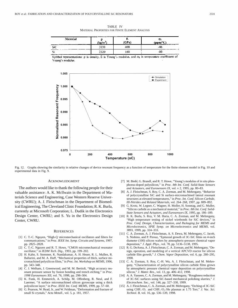
Fig. 12 presents graphs of normalized resonant frequencyversus temperature based on the results of the finite elementanalysis and the experimental data (vacuum conditions) that ispresented in Fig. 9. Although the geometry of the resonator infinite element model is different from the resonator that is actu-ally tested inside the SEM, there are certain similarities in thebehavior of resonant frequency with increasing temperature. Inboth cases, there is an initial steady decrease in resonant fre-quency, followed by a slight increase, and another slight de-crease. The differences between the finite element results andexperimental data can be attributed to differences in resonatorgeometry as well as variations between the actual material prop-erty parameters and those used in the model as well as the in-fluence of intrinsic stresses in the various material layers.
Examination of the material properties used in the finite el-ement model provides qualitative insight into the resonant fre-quency versus temperature behavior for the polySiC resonators.The thermal expansion coefficient of SiC is lower than that ofsilicon from 22 C to 200 C, while at higher temperatures,the thermal expansion coefficient of SiC is greater than that ofsilicon. Consequently, at temperatures below 200C, the sil-icon substrate expands faster than the polySiC layer, which in-duces a resultant compressive thermal stress in the suspensionbeams of the resonator. This scenario is consistent with resultsof the finite element analysis, which shows that the anchoredends of the suspension beams of the modeled resonator expe-rience 5 MPa compressive stress at 177C. The net effect ofthe induced compressive stress in the suspension beams and de-crease in Young’s modulus of polySiC leads to a decrease in theresonant frequency. As temperature increases above 200C, thepolySiC film begins to expand faster than the silicon substrate,which induces a resultant tensile stress in the resonator suspen-sion beams. This shift in stress is also consistent with resultsof the finite element analysis, which shows that the anchoredends of the suspension beams of the modeled resonator expe-rience 60 MPa tensile stress at 727C. Consequently, the low-ering effect on the resonant frequency due to the decrease inYoung’s modulus is counteracted by the induced tensile stress,which tends to increase resonant frequency. The net effect ofincreasing tensile stress and decreasing Young’s modulus withincreasing temperature leads to a resonant frequency minimum( 475 C in Fig. 12), and then, an increase. However, as thetemperature increases even further (825 C in Fig. 12), the ef-fect of the decrease in Young’s modulus dominates, leading tothe eventual decrease in resonant frequency.
VI. CONCLUSION
PolySiC resonators have been fabricated by a surface mi-cromachining process using SiO, polysilicon, and Ni as theisolation, sacrificial, and contact metallization layers, respec-tively. The resonators are packaged using ceramic-based ma-terials, stainless steel fasteners, and nickel wirebonding proce-
2330 IEEE TRANSACTIONS ON ELECTRON DEVICES, VOL. 49, NO. 12, DECEMBER 2002
Fig. 9. Graphs showing variation of resonant frequency with temperature for two polySiC resonators—one tested at atmospheric pressure (760 torr) and the othertested under vacuum conditions (0.1–0.2 torr). At atmospheric pressure, the resonator excitation voltage is 150 Vpp and the device does not operate above 500 Cdue to breakdown of insulating SiOlayer. In contrast, the resonator operates at temperatures as high as 950C under vacuum conditions with an excitation voltageof 3.5 Vpp.
Fig. 10. Solid model of a 2�m-thick polySiC resonator investigated using finite element analysis. The suspension beams are 150�m long and 3�m wide.
Fig. 11. Graphs of the thermal expansion coefficients of polySiC and siliconas a function of temperature.
dures. Optical and SEM-based setups are built to test the devicesunder atmospheric pressure (760 torr) and vacuum conditions( 10 torr), as well as temperatures up to 950C. Resonator
s increase with vacuum level to as high as100 000 at 10torr at 22 C due to decreased damping-related energy dissipa-tion. Resonant frequency drifts of18 ppm/h under continuousoperation have been observed. Resonator packaging survivedrepeated pressure (10 –760 torr) and thermal (22–950C)cycling without failure. High temperature testing revealed thatdevice resonant frequency decreases by2% between 22 Cand 700 C, followed by a slight increase at 900C, and then,eventual decrease at 950C. Finite element analysis reveals thatchanges in resonant frequency with increasing temperature de-pend on the interplay between the decrease in Young’s modulusof polySiC and induced stress in the suspension beams of theresonators, which occurs due to mismatch in thermal expansioncoefficients of the polySiC film and the underlying substrate.
ROY et al.: FABRICATION AND CHARACTERIZATION OF POLYCRYSTALLINE SiC RESONATORS 2331
TABLE IVMATERIAL PROPERTIES FORFINITE ELEMENT ANALYSIS
Fig. 12. Graphs showing the similarity in relative changes of device resonant frequency as a function of temperature for the finite element model in Fig. 10 andexperimental data in Fig. 9.
ACKNOWLEDGMENT
The authors would like to thank the following people for theirvaluable assistance: A. K. McIlwain in the Department of Ma-terials Science and Engineering, Case Western Reserve Univer-sity (CWRU); A. J. Fleischman in the Department of Biomed-ical Engineering, The Cleveland Clinic Foundation; R. K. Burla,currently at Microsoft Corporation; L. Dudik in the ElectronicsDesign Center, CWRU; and S. Yu in the Electronics DesignCenter, CWRU.
REFERENCES
[1] C. T.-C. Nguyen, “High-Q micromechanical oscillators and filters forcommunications,” inProc. IEEE Int. Symp. Circuits and Systems, 1997,pp. 2825–2828.
[2] C. T.-C. Nguyen and R. T. Howe, “CMOS micromechanical resonatoroscillator,” in IEDM Tech. Dig., 1993, pp. 199–202.
[3] H. Kahn, S. Stemmer, K. Nandakumar, A. H. Heuer, R. L. Mullen, R.Ballarini, and M. A. Huff, “Mechanical properties of thick, surface mi-cromachined polysilicon films,” inProc. Int. Workshop on MEMS, 1996,pp. 343–348.
[4] C. J. Welham, J. Greenwood, and M. M. Bertioli, “High accuracy res-onant pressure sensor by fusion bonding and trench etching,” inProc.1998 Eurosensors XII, vol. 76, 1998, pp. 298–304.
[5] K. Funk, H. Emmerich, A. Schilp, M. Offenberg, R. Neul, and F.Laermer, “A surface micromachined silicon gyroscope using a thickpolysilicon layer,” inProc. IEEE Int. Conf. MEMS, 1999, pp. 57–60.
[6] G. Pearson, W. Read, Jr., and W. Feldman, “Deformation and fracture ofsmall Si crystals,”Acta Metall., vol. 5, p. 181, 1957.
[7] M. Biebl, G. Brandl, and R. T. Howe, “Young’s modulus ofin situphos-phorus-doped polysilicon,” inProc. 8th Int. Conf. Solid-State Sensorsand Actuators, and Eurosensors IX, vol. v 2, 1995, pp. 80–83.
[8] A. J. Fleischman, S. Roy, C. A. Zorman, and M. Mehregany, “Behaviorof polycrystalline SiC and Si surface-micromachined lateral resonantstructures at elevated temperatures,” inProc. Int. Conf. Silicon Carbide,III-Nitrides and Related Materials, vol. 264–268, 1997, pp. 889–892.
[9] G. Krotz, W. Legner, C. Wagner, H. Moller, H. Sonntag, and G. Muller,“Silicon carbide as a mechanical material,” inProc. 8th Int. Conf. Solid-State Sensors and Actuators, and Eurosensors IX, 1995, pp. 186–189.
[10] R. K. Burla, S. Roy, V. M. Haria, C. A. Zorman, and M. Mehregany,“High temperature testing of nickel wirebonds for SiC devices,” inProc. Conf. Design, Characterization, and Packaging for MEMS andMicrolectronics, SPIE Symp. on Microelectronics and MEMS, vol.3893, 1999, pp. 324–333.
[11] C. A. Zorman, A. J. Fleischman, A. S. Dewa, M. Mehregany, C. Jacob,S. Nishino, and P. Pirouz, “Epitaxial growth of 3C-SiC films on 4-inchdiameter (100) silicon wafers by atmospheric-pressure chemical vapordeposition,”J. Appl. Phys., vol. 78, pp. 5136–5138, 1995.
[12] R. G. DeAnna, A. J. Fleischman, C. A. Zorman, and M. Mehregany, “De-sign, operation, and modeling of a vertical APCVD reactor for siliconcarbide film growth,”J. Chem. Vapor Deposition, vol. 6, pp. 280–295,1998.
[13] C. A. Zorman, S. Roy, C.-H. Wu, A. J. Fleischman, and M. Mehre-gany, “Characterization of polycrystalline silicon carbide films grownby atmospheric pressure chemical vapor deposition on polycrystallinesilicon,” J. Mater. Res., vol. 13, pp. 406–412, 1998.
[14] A. A. Yasseen, C. A. Zorman, and M. Mehregany, “Roughness reductionof 3C-SiC surfaces using SiC-based mechanical polishing slurries,”J.Electrochem. Soc., vol. 146, pp. 327–330, 1999.
[15] A. J. Flesichman, C. A. Zorman, and M. Mehregany, “Etching of 3C-SiCusing CHF /O and CHF /O /He plasmas at 1.75 Torr,”J. Vac. Sci.Technol. B, vol. 16, pp. 536–539, 1998.
2332 IEEE TRANSACTIONS ON ELECTRON DEVICES, VOL. 49, NO. 12, DECEMBER 2002
[16] W. Tang, “Electrostatic comb drive for resonant sensor and actuator ap-plications,” Ph.D. dissertation, Dept. EECS, Univ. California, Berkeley,1990.
[17] C. T.-C. Nguyen, “Micromechanical signal processors,” Ph.D. disserta-tion, Dept. EECS, Univ. California, Berkeley, 1994.
[18] A. J. Fleischman, “Silicon carbide for high temperature microelectrome-chanical systems,” Ph.D. dissertation, Dept. EECS, Case Western Re-serve Univ., Cleveland, OH, 1999.
[19] A. J. Fleischman, X. Wei, C. A. Zorman, and M. Mehregany, “Surfacemicromachining of polycrystalline SiC deposited on SiOby APCVD,”in Proc. Int. Conf. Silicon Carbide, III-Nitrides and Related Materials,vol. 264–268, 1997, pp. 885–888.
[20] R. G. DeAnna, S. Roy, C. A. Zorman, and M. Mehregany, “Modeling ofSiC lateral resonant devices over a broad temperature range,” inProc.Int. Conf. Modeling and Simulation of Microsystems, 1999, pp. 644–647.
[21] R. R. Reeber and K. Wang, “Thermal expansion and lattice parametersof group IV semiconductors,”Mater. Chem. Phys., vol. 46, pp. 259–264,1996.
[22] R. R. Reeber and K. Wang, “Thermal expansion of beta-SiC, GaP andInP,” in Proc. Symp. Covalent Ceramics III—Science and Technology ofNon-Oxides, MRS Fall Meeting, vol. 410, 1995, pp. 211–216.
Shuvo Roy(M’95) received the B.S. degree (magnacum laude) with General Honors for triple majorsin physics, mathematics (Honors), and computerscience from Mount Union College, Alliance, OH,in 1992. He received the M.S. and Ph.D. degrees inelectrical engineering from Case Western ReserveUniversity, Cleveland, OH in 1995 and 2001, respec-tively. While pursuing his doctorate, he conductedresearch in the areas of design, microfabrication,packaging, and performance of MEMS for harshenvironments.
He is a Co-Director of the BioMEMS Laboratory in the Department ofBiomedical Engineering at The Cleveland Clinic Foundation (CCF). He alsoinvestigated microstructural characteristics and mechanical properties ofMEMS materials, developed the requisite microfabrication technologies anddemonstrated operation of the first surface-micromachined silicon carbidetransducers at high temperatures (up to 950C). He has also developedminiaturized micro-relays for high performance electrical switching andice detection sensors for aerospace applications. He joined CCF in 1998 todevelop MEMS technology for various biomedical applications (BioMEMS)including surgical instruments, noninvasive monitoring, bioartificial organs,portable diagnostics, and drug delivery. He is also investigating new and novelmaterials for BioMEMS including polymers and natural proteins. He has over21 technical publications, co-authored one book chapter, and given over 20invited presentations.
Dr. Roy is the recipient of a Top 40 under 40 award by Crain’s Cleveland Busi-ness in 1999 and theClinical Translation Awardat the 2nd Annual BioMEMSand Biomedical Nanotechnology World 2001 meeting.
Russell G. DeAnnareceived the B.S. degree in me-chanical engineering from The Ohio State University,Columbus, in 1982, the M.S. degreefrom the Univer-sity of California, Berkeley, in 1985 and the Ph.D. de-gree in mechanical and aerospace engineering fromCase Western Reserve University (CWRU), Cleve-land, OH, in 1993.
He worked at General Electric Nuclear EnergyBusiness, San Jose, CA in reactor safety analysis be-fore joining NASA Glenn Research Center at LewisField, Cleveland, in 1985. At NASA Glenn, he was
employed by the Vehicle Technology Center of the Army Research Laboratory(ARL). This laboratory is the critical link between the scientific and militarycommunities. He has developed expertise in both empirical testing and ana-lytical modeling of turbo machinery components. He later worked on MEMSsensors and instrumentation for gas-turbine engines with ARL/NASA in col-laboration with Prof. Mehran Mehregany of CWRU. In 2000, he joined MovazNetworks, a telecommunications company developing an all-optical, cross con-nect. He is the principal designer of the MEMS micro-mirror switch. He joinedAdvanced Engineering Technologies, Norcross, GA, in late 2002 to work on fi-nite element modeling and analysis applications.
Christian A. Zorman (M’96) received the B.S. de-gree (cum laude) in physics and the B.A. degree (cumlaude) in economics from the The Ohio State Uni-versity, Columbus, in 1988, and the M.S. and Ph.D.degrees in physics from Case Western Reserve Uni-versity (CWRU), Cleveland, OH, in 1991 and 1994,respectively. His doctoral research involved an inves-tigation of the secondary electron emission propertiesof CVD diamond films for vacuum electronics.
Dr. Zorman joined the MEMS program at CWRUin 1994 as a Research Associate and immediately
began working in the SiC MEMS area. He was promoted to Senior ResearchAssociate in 1997 and Researcher in 2000. In addition to his research positionswithin the University, he has held appointments as Adjunct Assistant Professorin the Department of Electrical Engineering and Computer Science and InterimAdministrative Director of the Microfabrication Laboratory. He currently isan Associate Professor in EECS at CWRU. He has been instrumental in theconstruction of AP- and LPCVD reactors for SiC thin films, and has led thedevelopment of recipes for the growth of single and polycrystalline 3C-SiCfilms for micromachined sensors and actuators. In addition to the developmentof novel bulk and surface micromachining techniques for SiC, he was a keycontributor in the development of novel polishing, wafer bonding, and lowdefect density growth processes for SiC. He has published over 85 technicalpapers, two book chapters, and has taught several short courses on SiC forMEMS.
Dr. Zorman is a past chairman of the MEMS Technical Group in the Amer-ican Vacuum Society and is currently serving as co-chairman.
Mehran Mehregany (SM’00) received the B.S.in electrical engineering from the University ofMissouri, Columbia, in 1984, and the M.S. andPh.D. degrees in electrical engineering from theMassachusetts Institute of Technology, Cambridge,in 1986 and 1990, respectively.
From 1986 to 1990, he was a consultant to theRobotic Systems Research Department at AT&TBell Laboratories, where he was a key contributor toground-breaking research in microelectromechanicalsystems (MEMS). In 1990, he joined the Department
of Electrical Engineering and Applied Physics at Case Western Reserve Uni-versity (CWRU), Cleveland, OH, as an Assistant Professor. He was awardedthe Nord Assistant Professorship in 1991, was promoted to Associate Professorwith tenure in July 1994, and was promoted to Full Professor in July 1997. Heheld the George S. Dively Professor of Engineering Endowed Chair from Jan-uary 1998 until July 2000, when he was appointed the BFGoodrich Professorof Engineering Innovation. He served as the Director of the MEMS ResearchCenter at CWRU from July 1995 until July 2000. He is well known for his re-search in the area of MEMS, and his work has been widely covered by domesticand foreign media. He has over 200 publications describing his work, holds 12U.S. patents, and is the recipient of a number of awards/honors. He served asthe Editor-in-Chief of theJournal of Micromechanics and Microengineeringfrom January 1996 to December 1997, and is Assistant-to-the-President of theTransducers Research Foundation. His research interests include silicon andsilicon carbide MEMS, micromachining and microfabrication technologies,materials and modeling issues related to MEMS and IC technologies, andMEMS packaging. He is the Founder and served as the President (July 1993 toMarch 1999) of Advanced Micromachines Incorporated, Cleveland, a companyin the MEMS area. Advanced Micromachines Incorporated was acquired byThe BFGoodrich Corporation in March 1999. He founded NineSigma, Inc.,an information technology company, in February 2000 and served as its CEO(June 2000 to January 2001) and CTO (January 2001 to August 2001), duringwhich period he successfully completed initial rounds of private financing andgrew the company to 15 employees. He co-founded FiberLead, Inc., an opticaltelecommunications company, in September 2000 and served as its CEO untilSeptember 2001; during which period he successfully completed the early stageround of venture capital financing and grew the company to five employees.