3
2 5 a a, b b a b 2 5 2 × 2 μ 2 2 5 2 5 -1 2 3 2 3 IV 2 5 IV 2 5 2 2 5 2 ×10 -6 2 × 10 -6 2 5 2 5 2 × 2 μ 2

Vol. 127 (2015) ACTA PHYSICA POLONICA A No. 4
Proceedings of the 4th International Congress APMAS2014, April 24-27, 2014, Fethiye, Turkey
Fabrication and Characterization of Vanadium/Vanadium
Pentoxide/Vanadium (V/V2O5/V) Tunnel Junction DiodesM.F. Ziaa, M.R. Abdel-Rahmana,*, N.F. Al-Khallib, N.A. Debbarb
aPrince Sultan Advanced Technologies Research Institute (PSATRI), College of Engineering,
King Saud University, Riyadh 11421, Saudi ArabiabElectrical Engineering Department, College of Engineering, King Saud University, Riyadh 11421, Saudi Arabia
A metal/insulator/metal (MIM) diode is a structure in which a thin oxide layer is sandwiched between twometal layers. Metal/insulator/metal (MIM) diodes coupled to antennas have been widely investigated as detectorsfor millimeter wave and infrared radiation for imaging and spectroscopic applications. In this work, we report on thefabrication and characterization of MIM tunnel junction diodes by using a new material combination, vanadium-vanadium pentoxide-vanadium (V/V2O5/V), with contact areas of 2×2 µm2. The V/V2O5/V MIM was fabricatedusing electron-beam lithography, sputter deposition and conventional lifto methods. The fabricated V/V2O5/VMIM diodes showed a maximum absolute sensitivity of 2.35 V−1. In addition, noise spectra for the fabricated MIMdiodes were measured and analyzed.
DOI: 10.12693/APhysPolA.127.1289
PACS: 85.30.Kk
1. Introduction
A metal/insulator/metal (MIM) diode is a device hav-ing a thin oxide layer sandwiched between two metal lay-ers, where electrons pass from rst metal layer to sec-ond metal layer through a thin oxide layer by quantumtunneling process [1]. Quantum tunneling occurs only ifthe oxide layer is less than or equal to 4 nm [2]. Metal-insulator-metal diodes are usually designed to have smallcontact areas, compared to the wavelengths of the inci-dent radiation, in order to satisfy required cut-o fre-quencies. Due to the compulsory small contact areas ofMIM diodes, antennas are usually coupled to the MIMdiodes in order collect incident electromagnetic radia-tion. Antenna-coupled MIM diodes have been widelyinvestigated for millimeter wave and infrared detection[35] due to several inherent advantages of the structure:fast response, easy fabrication compared to other mil-limeter wave and infrared detectors, low power consump-tion, easy to integrate to read-out integrated circuits(ROICs), and uncooled operation [6]. So far many mate-rial combinations such as Ni/NiO/Ni [3, 4], Al/Al2O3/Pt[5], Al/Al2O3/Al [6], Ni/NiO/Au [7], Cu/CuO/Cu [8],Cu/CuO/Au [9], and others have been studied aiming atMIM diodes with highly nonlinear current-voltage (I-V )behavior to achieve high sensitivities.In this work, we fabricate and characterize thin lm
based MIM tunnel junction diodes using a novel materialcombination, vanadium-vanadium pentoxide-vanadium(V/V2O5/V). The MIM diodes are manufactured us-ing electron-beam lithography (e-beam) and lifto tech-niques. The diode junction is fabricated using direct cur-
*corresponding author; e-mail: [email protected]
rent (DC) sputtering for the deposition of the metal elec-trodes and radiofrequency (RF) diode sputtering for thedeposition of the thin oxide layer. I-V characteristicswere measured in order to study the dynamic resistanceand sensitivity of diode. The theoretical Simmons equa-tion for tunneling current was employed to analyze theexperimental results and quantify the MIM diode param-eters. In addition, noise spectrum of the fabricated MIMdiode was measured and analyzed.
2. Device fabrication
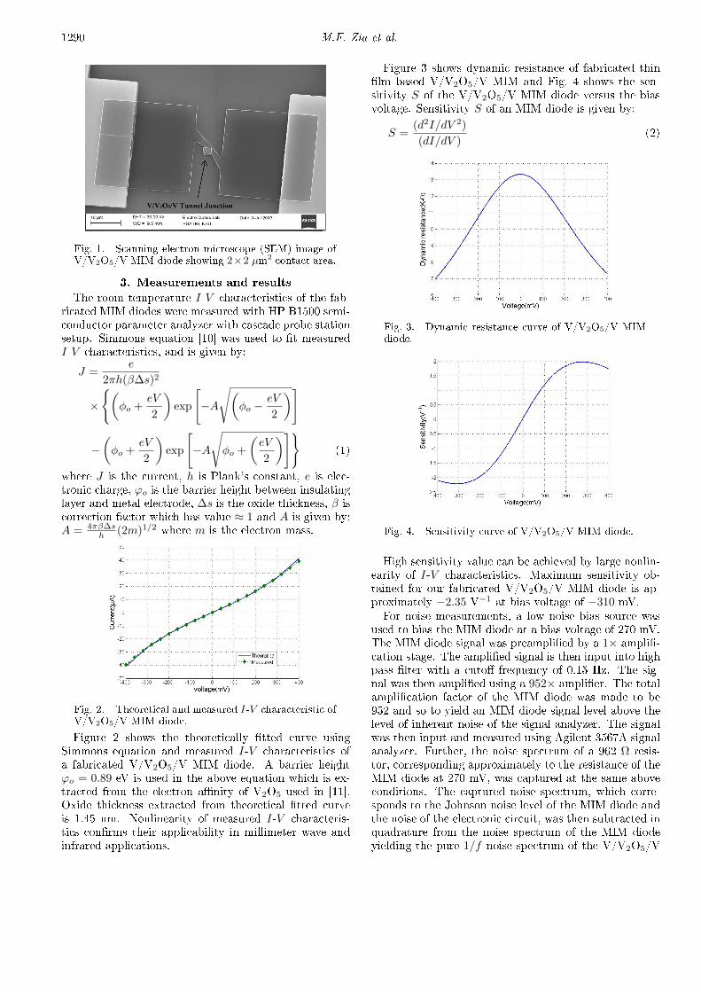
The V/V2O5/V MIM diodes were fabricated on sili-con (Si) substrate with 300 nm of silicon dioxide (SiO2)layer thermally grown on top of it for the purpose ofelectrical isolation. Electron-beam lithography was usedfor patterning the MIM diodes. The e-beam resist pro-cessing parameters, exposure and development processesparameters, lifto process and contact pad patterning arein detail described in [8] for Cu/CuO/Cu MIM diodes;the same process was applied in this work for fabricat-ing V/V2O5/V MIM diodes. The rst V electrode of thestructure, 100 nm thick, was deposited using DC sput-tering at 150 W of power, a chamber base pressure of2×10−6 Torr and Argon (Ar) pressure of 3 mTorr. Vana-dium pentoxide was RF diode sputtered for 3 minutes ontop of the rst V electrode at 150W of RF power, a cham-ber base pressure of 2 × 10⁻⁶ Torr and Argon (Ar) pres-sure of 3 mTorr. Lifto process was performed overnightto remove V and V2O5 layers deposited on unexposedregions to get patterned rst electrode. The second elec-trode was deposited under the same conditions as therst electrode. Figure 1 shows a scanning electron mi-croscope (SEM) image of a fabricated V/V2O5/V MIMdiode with 2 × 2 µm2 contact area.
(1289)
1290 M.F. Zia et al.
Fig. 1. Scanning electron microscope (SEM) image ofV/V2O5/V MIM diode showing 2×2 µm2 contact area.
3. Measurements and results
The room temperature I-V characteristics of the fab-ricated MIM diodes were measured with HP B1500 semi-conductor parameter analyzer with cascade probe stationsetup. Simmons equation [10] was used to t measuredI-V characteristics, and is given by:
J =e
2πh(β∆s)2
×
(φo +
eV
2
)exp
[−A
√(φo −
eV
2
)]
−(φo +
eV
2
)exp
[−A
√φo +
(eV
2
)](1)
where J is the current, h is Plank's constant, e is elec-tronic charge, ϕo is the barrier height between insulatinglayer and metal electrode, ∆s is the oxide thickness, β iscorrection factor which has value ≈ 1 and A is given by:A = 4πβ∆s
h (2m)1/2 where m is the electron mass.
Fig. 2. Theoretical and measured I-V characteristic ofV/V2O5/V MIM diode.
Figure 2 shows the theoretically tted curve usingSimmons equation and measured I-V characteristics ofa fabricated V/V2O5/V MIM diode. A barrier heightϕo = 0.89 eV is used in the above equation which is ex-tracted from the electron anity of V2O5 used in [11].Oxide thickness extracted from theoretical tted curveis 1.45 nm. Nonlinearity of measured I-V characteris-tics conrms their applicability in millimeter wave andinfrared applications.
Figure 3 shows dynamic resistance of fabricated thinlm based V/V2O5/V MIM and Fig. 4 shows the sen-sitivity S of the V/V2O5/V MIM diode versus the biasvoltage. Sensitivity S of an MIM diode is given by:
S =(d2I/dV 2)
(dI/dV )(2)
Fig. 3. Dynamic resistance curve of V/V2O5/V MIMdiode.
Fig. 4. Sensitivity curve of V/V2O5/V MIM diode.
High sensitivity value can be achieved by large nonlin-earity of I-V characteristics. Maximum sensitivity ob-tained for our fabricated V/V2O5/V MIM diode is ap-proximately −2.35 V−1 at bias voltage of −310 mV.For noise measurements, a low noise bias source was
used to bias the MIM diode at a bias voltage of 270 mV.The MIM diode signal was preamplied by a 1× ampli-cation stage. The amplied signal is then input into highpass lter with a cuto frequency of 0.15 Hz. The sig-nal was then amplied using a 952× amplier. The totalamplication factor of the MIM diode was made to be952 and so to yield an MIM diode signal level above thelevel of inherent noise of the signal analyzer. The signalwas then input and measured using Agilent 3567A signalanalyzer. Further, the noise spectrum of a 962 Ω resis-tor, corresponding approximately to the resistance of theMIM diode at 270 mV, was captured at the same aboveconditions. The captured noise spectrum, which corre-sponds to the Johnson noise level of the MIM diode andthe noise of the electronic circuit, was then subtracted inquadrature from the noise spectrum of the MIM diodeyielding the pure 1/f noise spectrum of the V/V2O5/V

Fabrication and Characterization of Vanadium/Vanadium Pentoxide/Vanadium. . . 1291
MIM diode, Fig. 5. The resultant spectrum conrms thetypical dominant 1/f noise behavior in MIM diodes.
Fig. 5. Measured 1/f noise spectrum of V/V2O5/VMIM diode.
4. Conclusion
Thin lm V/V2O5/V MIM junctions have been ex-perimentally realized and characterized to demonstratetheir feasibility in millimeter wave and infrared detec-tion applications. The MIM diode was patterned bye-beam lithography, lifto and conventional sputteringtechniques. The thin insulating V2O5layer was depositedby RF diode sputtering. The I-V characteristics of thejunctions were measured, showing nonlinear behavior, azero bias resistance of 13.4 kΩ and a maximum abso-lute sensitivity of 2.35 V−1 at a bias voltage of 310 mV.Moreover, the noise spectrum of the V/V2O5/V MIMdiode was measured and analyzed showing a typical dom-inant 1/f noise behavior.
Acknowledgments
This work was supported by the Annual Grants Pro-gram at King Abdulaziz City for Science and Technology(KACST) under grant AT-32-74.
References
[1] A. Sanchez, C.F. Davis, K.C. Liu, A. Javan, J. Appl.Phys. 49, 5270 (1978).
[2] P. Dudek, R. Schmidt, M. Lukosius, G. Lupina,Ch. Wenger, A. Abrutis, M. Albert, K. Xu, A. Devi,Thin Solid Films 519, 5796 (2011).
[3] M.R. Abdel-Rahman, B. Monacelli, A.R. Weeks,G. Zummo, G.D. Boreman, Opt. Eng. 44, 066401(2005).
[4] C. Fumeaux, W. Herrmann, F.K. Kneubuhl,H. Rothuizen, Infrared Phys. Technol. 39, 123(1998).
[5] J.A. Bean, B. Tiwari, G.H. Bernstein, P. Fay,W. Porod, J. Vac. Sci. Technol. B 27, 11 (2009).
[6] P. Esfandiari, G. Bernstein, P. Fay, W. Porod,B. Rakos, A. Zarandy, B. Berland, L. Boloni, G. Bore-man, B. Lail, B. Monacelli, A. Weeks, SPIE Pro-ceedings, Infrared Technology and Applications XXXI5783, 470 (2005).
[7] A.B. Hoofring, V.J. Kapoor, W. Krawczoneck,J. Appl. Phys. 66, 430 (1989).
[8] M. Abdel-Rahman, M. Syaryadhi, N. Debbar, IETElec. Lett. 49, 363 (2013).
[9] M.N. Gadalla, M. Abdel-Rahman, A. Shamim, Sci.Rep. 4, 4270 (2014).
[10] J.G. Simmons, J. Appl. Physics 34, 1793 (1963).
[11] M. Minagawa, K. Nakai, A. Baba, K. Shinbo,K. Kato, F. Kaneko, C. Lee, J. Korean Phys. Soc.58, 1402 (2011).


![Mechanism of vanadium(V) oxidation of thallium(I) in aqueous …nopr.niscair.res.in/bitstream/123456789/41342/1/IJCA 35A(5) 416-42… · [vanadium(V)]. Initial rates were reproducible](https://static.documents.pub/doc/80x56/5f1307e4bf30dc75f36b8c3b/mechanism-of-vanadiumv-oxidation-of-thalliumi-in-aqueous-nopr-35a5-416-42.jpg)


![Determination and Quantification of Vanadium(V) in ... · fume [8]. Therefore, the determination of vanadium in environmental samples is necessary in terms of environ- mental protection.](https://static.documents.pub/doc/80x56/5e225f0633b9cd6bf23506f2/determination-and-quantification-of-vanadiumv-in-fume-8-therefore-the.jpg)