Fabrication of Group IV Semiconductors on Insulator for Monolithic 3D Integration Ali Asadollahi Doctoral Thesis in Information and Communication Technology School of Electrical Engineering and Computer Science KTH Royal Institute of Technology Stockholm, Sweden 2017
Transcript
Fabrication of Group IV
Semiconductors on Insulator for
Monolithic 3D Integration
Ali Asadollahi
Doctoral Thesis in Information and Communication Technology
School of Electrical Engineering and Computer Science
KTH Royal Institute of Technology
Stockholm, Sweden 2017
ii
Akademisk avhandling som med tillstånd av Kungliga Tekniska högskolan
framlägges till offentlig granskning för avläggande av teknologie doktorsexamen
fredagen den 16 februari 2018 klockan 10:00 i Ka-Sal C (Sal Sven-Olof Öhrvik),
Electrum, Kungliga Tekniska högskolan, Kistagången 16, Kista.
Figure 2.2. Transistor performance in terms of leakage current [Source: Intel].
The innovation in CMOS technology are shown in Fig. 2.3. The drive current Ion is described as
Where L is the channel length, W is the width, is the gate capacitance, µ is effective carrier mobility and Vdd is the supply voltage [43].
Figure 2.3. Innovations in CMOS technology roadmap [43].
27
The basic requirement in scaling CMOS transistor is that it must electrostatically
hold together, and the gate plays a key role in fulfilling that purpose. The gate should
provide a high on current in the ‗ON‘ state while keeping the ‗OFF‘ state leakage
current to the lowest possible value [43].
As discussed above by continuing the scaling various problems arise which degrade
the MOSFET performance. The problems with scaling are briefly described below. In
a MOSFET gate terminal is built to control the charge carries (electrons or holes) in
the channel. The scaling theory provides guidelines in order to scale the MOSFET
dimensions without sacrificing its reliability and performance. In the simplest form of
scaling the vertical and horizontal dimension of the MOSFET and the supply voltage
will be scaled by the same factor to keep the electric field in the scaled MOSFET as
before (constant-field scaling). However in actual scaling, the geometry and supply
voltage are being reduced by different factors (generalized scaling). When the gate
length (Lg) is scaled by a factor α, then it is needed to scale down the gate oxide (tox),
depletion layer width (xd) and supply voltage (Vd) by the same factor to keep the
electric field as before in the scaled device [42], [45].
In long channel MOSFETs the vertical electric field in the channel induced by gate
is larger than the lateral electric field which is due to the drain voltage. In such devices
the physics of the transistor is divided into two parts, i.e. gate-controlled carrier
formation and drain-controlled carrier transport. The threshold voltage (VT), which is
the voltage when the MOSFET turns on, is only dependent on the gate voltage in long
channel devices. The subthreshold swing (SS) is a measure of how quickly the device is
switching from Off to On state. In other words, is the number of millivolts (mV)
required to increase the VG in order to produce a factor of 10 increase in the drain
current (ID). In normal MOSFET operation the SS is limited to be greater than KT/q
(60 mV/dec) at room temperature [45]. In short channel devices as the gate length is
reduced, the drain voltage control on the channel becomes stronger and it gets harder
for the gate to control the source barrier and the charges in the channel. In this case
we use 2D electrostatic effects which cause: a) a reduction in threshold voltage as the
gate length reduces (VT roll-off), b) a change and a reduction in VT as the drain voltage
increases (drain-induced-barrier-lowering, DIBL). c) a degradation in subthreshold
swing. These phenomena are called short channel effect (SCE) and they cause an
increase in off state leakage current. Therefore the MOSFET designer try to inhibit
these SCE effect in short channel devices. Every technique which has been used to
suppress SCE has its own drawbacks in term of performance and new static leakage
mechanism. One approach to reduce the short channel effects is to increase the gate
control over the channel. This can be obtained by thinning down the gate oxide.
Although, as the gate oxide gets thinned, due to the quantum mechanical tunneling the
Chapter 1. Introduction
28
gate leakage increases and subsequently the static power dissipation increases. One
solution is to replace the silicon dioxide (SiO2) as the gate oxide with a dielectric with
higher permittivity (high-k) e.g. zirconia (ZrO2) or hafnium (HfO2). Using high-k
material which has a higher capacitance allows us to use a thicker insulator to inhibit
the tunneling. However, introduction the high-k material as the gate insulator is
accompanied with new challenges such as surface roughness, interface trap, fixed
charge in insulator, etc. Another approach to suppress the SCE is to increase the
channel doping and terminating the electric field induced by the drain voltage.
However, as the doping in the channel increase the carrier mobility is reduced due to
the increased carrier scattering. In addition, the subthreshold swing gets degraded
because some parts of the gate voltage will be stolen from the surface by a higher
depletion capacitance in the channel. Besides, in the very high doping regions near the
source and drain extensions, band-to-band tunneling and consequently the leakage
current become higher [45], [46]. However, by keeping the doping in the middle of the
channel low while increasing the doping under the gate edges, one can benefit the new
doping profile; which inhibits leakage at the S/D with high carrier mobility and low
resistance in the part of the channel needed [43]. Such doping profile is obtained by a
tilted ‗halo‘ implant. The ‗shallow extension‘ and ‗local halo‘ are the fundamental
technique in device scaling since late 80‘s. The loss of gate control over channel when
channel length is scaled is represented in Fig. 2.4; by adding a shallow extension of the
S/D the gate recovers its control over channel.
Figure 2.4. Gate length scaling (a) long channel transistor, (b) short channel with S/D extensions, (c) short channel when gate voltage is applied.
By reducing the source/drain junction depth (near the gate edge) the SCE will be
suppressed by reducing the drain coupling to the source barrier. However, as the
29
junctions‘ depth gets reduced their doping should be increased in order to keep the
sheet resistance constant; in addition, the solid solubility of the dopants is limited
(~1020cm-3). Hence, the reduction in junction‘s depth makes an increase in the series
resistance in accessing the channel. In addition, by having ultra-shallow junctions it is
difficult to keep the junctions abrupt after annealing the dopants and their following
diffusion. All these phenomena will degrade the MOSFET performance. Therefore,
new materials and structures are needed to replace Si and have a potential to change
the conventional bulk MOSFETs in future [31], [33], [34], [41], [42], [47]. In order to
increase the drive current of the MOSFET, carrier transport needs to be enhanced and
there are various approaches to realize that, including: introducing strain into the
channel [32], [42], [48], [49] incorporating novel high mobility materials in the channel
[31], [33], [34], [36], [38] finding the optimal substrate and channel orientations [50],
[51], [52] or a combination of all of them.
2.1.1 The Effect of Strain on Mobility
NMOS) It has been shown in Si when a tensile strain is applied to Si in the channel
the conduction band will split [45], [53], and this splitting lead to an increase in the
electron mobility since the occupancy of the 2-fold valleys, which have a lower
effective mass, will be increased. The electron mobility enhancement by applying
tensile strain to Si channel using SiGe SRB has been reported previously on planar
long channel MOSFETs [45], [54]. Similar effect of electron mobility enhancement
due to the strain is expected in tensile strained SiGe films; yet there is no report on
nMOS tensile strained SiGe devices. In this thesis in Chapter 6.5 we propose, for the
first time, a fabrication method to realize tensile strain Si0.5Ge0.5OI substrates; however
nMOS devices have not been fabricated yet and are under production in our group.
In 2016, IBM and Samsung reported the 7 nm and 5 nm tensile strained Si Fins for the
NMOS transistor accompanied by compressive SiGe PMOSs, all epitaxially grown on
SiGe SRB [27], [28]. Figure 2.5.(a). illustrates the biaxial and uniaxial stress in the
device layer. Figure 2.5. (b). presents the long channel electron mobility enhancement
of 40% in tensile Si compare to unstrained Si fabricated by Samsung. A two times
boost in electron mobility in 7nm, tensile strained Si long channel FinFETs fabricated
on Si0.75Ge0.25 SRB is reported at the same time by IBM; the Fin structures are shown
in Fig. 2.5. (c)[27].
Chapter 1. Introduction
30
(a)
(b)
(c)
Figure 2.5.(a). Schematic view of biaxial and uniaxial stress with SiGe SRB [55]. (b) long channel electron mobility enhancement in tensile strained Si Fin on SiGe SRB [28]. (c) Schematic view and TEM view of dual stressed channel materials on SiGe SRB, with (left) tensile strained Si Fin (right)
Compressive strained SiGe Fin [27].
PMOS) The effect of strain on hole mobility is more complicated than electrons
[56], [57]. Here the strain splits the light hole and heavy hole bands and changes their
curvatures in the valance band. That causes the light hole band to shift upward on top
of the valance band which results in a lower effective mass and a higher mobility [51].
The effects of various strains on Si hole mobility are summarized in Fig 2.6.
31
Figure 2.6. Dependencies of the Si hole mobility on compressive and tensile strain (uniaxial and biaxial) [45], [51].
The biaxial tensile strain on Si in the channel can be implemented in various ways
such as 1) epitaxial growth of Si on relaxed SiGe buffer layer [58]. 2) making strained
Si/relaxed SiGe on buried oxides which results in strained Si on insulator [32]. 3)
bonding and transfer a strained Si layer directly to oxides [59]. Uniaxial compressive
strain on Si can be implemented by 1) selective epitaxial growth of SiGe in the
source/drain regions (for pMOSFETs) [57], [60]. 2) applying local strain using
techniques such as shallow trench isolation [61]. SiGe and Ge PMOS transistors have
shown higher hole mobility and improved performance compare to Si PMOS
transistors [10], [11], [62], [27], [28], [30], [44]. IBM and Samsung have chosen SiGe
PMOS transistors for their 5 nm and 7 nm FinFETs [27], [28].
Another approach to boost the performance of MOSFETs is fabrication of devices
on silicon on insulator (SOI) substrates, which can provide a solution for electrostatic
issues[61], [63]. Implementing SOI substrates offer a great opportunity for further
scaling the CMOS transistors. The buried oxide underlying the device layer can limit
the punch-through which may occur on very short gate length bulk devices. Novel
structures using semiconductors on insulator substrates such as double gate, FinFET,
and surrounding gate devices have become very attractive in recent MOSFET
technology[64]–[70]. However, Intel is still using bulk substrates for its novel 22 nm
and 14 nm trigate transistors [71]. In order to minimize the leakage currents while
delivering the high performance bulk Si transistors have become ever more complex,
adding additional levels of manufacturing complexity at an ever increasing rate. In
extremely reduced short channel devices[63], new solutions need to be found to
reduce complexity while bringing the benefits of reduce Si geometries that the industry
expects. Fully depleted Si on insulator (FDSOI) is an approach to deliver these
benefits while enabling a simplification of the manufacturing process [72]. FDSOI
does not change the fundamental geometry of the transistor. In FDSOI the innovation
Chapter 1. Introduction
32
lies in adding a thin layer of insulator called the buried oxide positioned just below the
channel and eliminating the need to add dopants to the channel thus making it fully
depleted. Another key, innovative step is that the Si on oxide layer is very thin and this
technology is called Ultra-Thin Body and Buried oxide (UTBB)[64]–[70]. Now we
look how FDSOI makes the better transistor performance. On a same technology
node, the FDSOI transistor has a shorter effective channel compare to a bulk Si
implementation. The shorter channel reduces the time necessary for the electrons flow
from the source to the drain, leading to a faster transistor. In order to improve
transistor performance a voltage can be applied to the substrate this method called
body biasing, that facilitates the creation of the channel between the source and the
drain, resulting in faster switching of the transistor. In FDSOI due to the presence of
the thin insulator below the channel, the biasing creates a buried gate below the
channel making the FDSOI work like a vertical double gate transistor. In bulk
technology the ability to do body biasing is very limited due to the parasitic current
leakage. The buried gate on the FDSOI transistor prevents any leakage in the
substrate; this allows a much higher voltage on the body leading to a significant boost
in performance. An FDSOI chip is able to operate at a lower voltage than its bulk
counterpart while delivering the same level of performance this makes the FDSOI
chip cooler with lower power consumption. The characteristics of the FDSOI vertical
double gate transistor allow the creation of new concept in processors design; different
voltages can be applied independently to the top and to the buried gates which
effectively change the characteristic of the transistor. By choosing optimal
combination of the voltages on the top and buried gates, the transistors characteristics
can be transformed from those of a very high performance transistor to those of a
very low power transistor, a processing core built up of such transistors can operate as
if it were in fact two cores: one optimized for high performance and the other for low
power[71], [73], [74]. If the device layer on insulator is between 20-40 nm some un-
depleted regions remain; such devices are called partially depleted SOI (PDSOI); while
for thicknesses below 10 nm fully depleted SOI is achieved (FDSOI). Figure 2.7.
represents transistors built on various substrates such as bulk Si, PDSOI and FDSOI.
The junction leakage is significantly reduced using FDSOI substrates.
33
Figure 2.7. Schematic image of MOS transistors built on (a) Bulk silicon (b) partially depleted SOI
(PDSOI) and (c) fully depleted SOI (FDSOI) substrates.
In industry Intel has been manufacturing FinFETs in volume on bulk Si substrate
since 2011 starting with its 22nm node processors. And nowadays14 nm node is under
production by Intel. Intel 14 nm technology has dimensional scaling compare to 22
nm. The transistor fins are taller, thinner, and more closely packed for improved
density and lower capacitance[75]. Figure 2.8. illustrates 3D images of Intel‘s 22 nm
and 14 nm FinFETs.
(a)
(b) Figure 2.8. Schematic figure of the Intel 22 nm FinFETs (a) and 14 nm FinFETs (b). (the picture are
the snapshots of the intel video in [75])
In 14-nm technology node, Intel is using advanced doping techniques to maintain
low doped fins and prevent the leakage current under the fins. The saturated drive
current of the Intel 14nm FinFETs is 15% higher for the NMOS and 41% higher for
the PMOS transistors compare to the Intel's 1st generation 22nm FinFETs.
Employing FinFET structures suppresses leakage in short channel transistors by
Chapter 1. Introduction
34
wrapping the gate around the fin and have more electrostatic control of the gate over
channel. The wrapped gate around the fin can fully or nearly-fully depletes the channel
and inhibits the leakage current; therefore, it makes it possible to use either bulk or
SOI substrates.
IBM has produced 14nm FinFETs on SOI [76], but In 2016, IBM and Samsung
announced 7 nm and 5 nm tensile strained Si Fins for the NMOS and compressive
Another approach to extend the CMOS scaling is the integration of novel high
mobility materials such as Ge, strained SiGe, III-V group, Graphene, etc. into the
channel. Due to the on-current saturation (Ion) in scaling conventional Si transistors,
high mobility materials into the channel can further increase the on-current [42], [58].
In very short channel Si transistors this saturation phenomenon is limited by injection
velocity from source to channel (vs) [77]–[79]. Furthermore, it has been shown
experimentally that the measured carrier velocity is proportional with the low field
effective mobility (µeff)[80]. Therefore, high mobility materials lead to higher Vinj and
consequently higher Ion. The performance metrics such as drive current and gate delay
can be written in terms of Vinj , showing the advantage of employing high mobility
materials.
2.1
2.2
Where Qinv is the inversion layer charge density, τ is the logic gate delay, VDD is the
supply voltage, Lg is the gate length, CL is the load capacitance, , and Vt is the
threshold voltage. By substituting 1.1 into 1.2 it can be identified that implementing
high mobility materials which lead to higher Vinj and higher IDsat cause a reduction in
gate delay τ [42]. Ge is a group IV element with zinc blend crystal structure like Si.
While the first transistors were made of Ge it was replaced by Si due to the high
electrical quality of thermal SiO2 and low defect high quality Si/SiO2 interface.
However, by aggressive scaling of Si MOSFETs in order to achieve better
performance and higher packing density, the SiO2 thickness should be scaled down
below 2nm. At this thickness tunneling current through the SiO2 becomes unbearable.
Therefore, it was necessary to replace the SiO2 gate insulator with another insulator
with higher permittivity in order to increase the capacitance and keeping the required
thickness to prevent tunneling. At this point the high-k materials started a new era in
CMOS industry [32], [81]. By changing the gate insulator from SiO2 to high-k materials
35
Ge got back to focus since it has the highest hole mobility among semiconductors and
a higher electron mobility than Si (Table.2.1)[81]. The fundamental physical properties
of Si, Ge and different SiGe compositions are listed in Table 2.1.
Ge has smaller effective mass (mt) for electrons and smaller effective masses for
heavy hole (mhh) and light hole (mlh) compare to Si, and a smaller effective mass lead
to higher mobility. Table 1.2 shows the bulk mobility comparison between Ge, Si and
III-V materials[41].
Material
Property
Si Ge GaAs InAs InSb
Electron mobility (cm2/V-s)
1600 3900 9200 40000 77000
Hole mobility (cm2/V-s)
430 1900 400 500 850
Bandgap (eV) 1.12 0.66 1.424 0.36 0.17
Dielectric constant
11.8 16 12.4 14.8 17.7
Table 2.1. bulk mobility comparison of various semiconductors.
Some groups have performed various simulations on Ge MOSFETs to benchmark
their performance. Considering different architectures, substrate orientations, channel
directions and strain effects for Ge pMOS and nMOS. For PMOS a systematic
comparison has been performed on strained Ge nano-scale (Lg=15nm, tox=0.7nm and
Vdd=0.7V) p-DGFETs[82]. Different simulation techniques have been employed to
accurately capture the essentials of device metric including strain (uniaxial and biaxial,
compressive and tensile), mobility, drive current, substrate orientation, channel
direction, switching delay and off-state leakage [82]. In general, Ge has 2X higher
mobility than Si and the trend for both in terms of orientation is (110)>(111)~(001).
The highest mobility for both is along (110)/[-110] with Ge~285 (cm2/V-s) and
Si~215 (cm2/V-s) [82].
There are several experimental results of hole mobility enhancements in Ge p-
MOSFETs [10], [83], [84]. Experimental results from compressive biaxial strained Ge
p-MOSFET fabricated on strained relaxed SiGe buffer with 45-55 % Ge has been
shown to yield a 8x higher inversion hole mobility (p=770 cm2/Vs) compared to Si
universal hole mobility. The device has been fabricated on (100) Ge surface along
<110> direction [10]. For uniaxial compressive strain in the <110> direction 15x
Chapter 1. Introduction
36
higher hole mobility has been demonstrated[84]. Table 2.2 presents a summary of
some of the highest experimentally recorded Ge hole motilities.
Hole mobility
(Ns=5x1012 cm-2)
structure
technique Reference
1500 uniaxial compressive strain NW
high k, trigate, metal gate
bonding MIT[11]
855 uniaxial compressive NW
metal S/D, Al2O3 dielectric
Condensation K.Ikeda[83]
770 biaxial compressive
strain
high k, metal gate, implanted S/D
SiGe buffer Intel[10]
250 Strain-relaxed Ge MOSFET
High k, metal gate, implanted S/D
SiGe buffer Intel[10]
100 Si Universal
Table 2.2. Previously published results for non-planar and state of the art planar Ge-pFETs with high-k dielectrics.
2.2 GeOI Fabrication Techniques
By considering the superior carrier transport in Ge over Si, one can benefit from
the advantages of SOI substrate, mentioned earlier, to fabricate high performance
MOSFETs using germanium on insulator (GeOI) substrates. The small band gap of
Ge results in high leakage currents in Ge MOSFETs and high dielectric constant of
Ge increases the short channel effect. However, by employing a thin Ge layer on
insulator one can suppress these effects. GeOI substrates are gaining a lot of attention
as a high mobility material with the advantages of the on insulator platform for further
boost the performance and more physical stability compare to fragile bulk Ge
substrates. Furthermore, they have been considered as a template for high quality
GaAs epitaxy[14]. Now we briefly review the main fabrication techniques for GeOI:
37
2.2.1 SIMOX, Liquid Phase Epitaxy and Smart Cut Techniques
SIMOX
Separation by implanted oxygen (SIMOX) is one of the methods to fabricate
semiconductor on insulator materials. It works by implanting high doses of hydrogen
followed by a high temperature annealing to remove implant damages and form a
buried oxide layer. When applied to Si it results in a good uniformity and a low defect
density. SIMOX is one of the few techniques in SOI technology that is capable of
supporting thin film SOI application, in volume production. It is not possible to use
SIMOX technique to fabricate silicon germanium on insulator (SGOI) with Ge
content more than 30%, because implantation needs a high temperature >1300 °C
post-annealing in order to heal the defects. Therefore, such a high annealing
temperature results in melting and surface oxidation of SiGe or Ge [85].
Figure 2.8. Principle of SIMOX process[86].
Ge Condensation
In this process first a SiGe layer with low content of Ge is grown on a thinned SOI
(formed by SIMOX) substrate[85], [87]. Due to the oxidation, SiGe layer forms a
Chapter 1. Introduction
38
mixed oxide of SiO2 and GeO2. At high temperatures GeO2 formation is reducing due
to the steady usage of Si to form SiO2 layer and repelling Ge (i.e. GeO2 +Si→SiO2
+Ge). At high temperatures while the SiO2 layer grows, Ge is repelled from the SiGe
layer and condenses into the underlying Si layer and forms SGOI [85], [87]. As the
oxidation proceeds, the thickness of the SiGe layer decreases and the Ge fraction
increases. The total Ge amount is conserved; therefore, the final Ge fraction depends
on initial Ge fraction in SiGe layer and its final thickness. The final high Ge content
layer can be as thin as 7 nm and it has a small compressive strain which will boost the
hole mobility as we discussed earlier [85], [88]. However, fabricated Ge MOSFETs on
GeOI substrate made by condensation process exhibited a large off state leakage
current due to the large amount of defects in Ge layer [88]. In Ge condensation
technique there is a lose control over threading dislocation nucleation. By applying the
condensation technique to micron-sized mesa structures one can eliminates the
dislocation formation but with a trade off in the active area‘s size [81], [85].
(a) (b)
Figure 2.9. Schematic of the condensation technique (a) epitaxial growth of SiGe layer on an SOI with low Ge content. (b) Following oxidation at high temperature causes the Ge repulsion into the
underlying SiGe layer and forming high Ge content SiGe on insulator.
Liquid Phase Epitaxy (LPE)
Due to the low melting point of Ge researchers use this method to form GeOI
from liquid Ge [89], [90]. First a SiN layer is deposited on Si substrate and seed
windows are patterned on SiN layer. A layer of Ge is deposited, by evaporation,
sputtering or PECVD. Then, the Ge layer is patterned into rectangular shapes with a
width of few microns and a length of tens of microns. After that the structures are
covered with PECVD SiO2 layer. Next, a rapid thermal annealing (RTA) just above
the melting point of Ge for few seconds is performed; a natural cool-down initiates in
regions where Ge is in contact with Si and proceeds to the regions on insulator
39
(SiN)[81]. The Ge layer follows the crystal structure of the Si seed layer. As the solid
Ge layer gets thicker it forms threading dislocations along (111) planes to release the
strain in the lattice and relaxes. The dislocations terminate on the SiO2 layer and result
in a dislocation free Ge layer on insulator[81]. The etch pit density (EDP) below
cm-2 was reported for GeOI layers fabricated using this process [88], [81].
The surface roughness of the LPE Ge is similar to the deposited Ge and RMS values
of 1.98 nm for the deposited layer and 2.11 nm for LPE layer have been reported[80],
[88]. However, the lateral length of the solidified low defect density Ge layer is limited
to typically 20 mm [14], [81].
Figure 2.10. Schematic figure of the LPE growth of the Ge layer on the Si seed layer and its lateral extension on insulator.
Bonding and Etch-Back
a) Grinding and SmartCut (without a stop layer)
In order to achieve high quality, low TDD layers of Si, SiGe or Ge on insulator, a
method to incorporate such high quality layers directly onto insulator is preferred. This
can be obtained via wafer bonding of a donor wafer consisting of a thick transfer layer
(Si, SiGe or Ge) to oxidized handle wafers[91]. The successful direct bonding process
requires a surface roughness below 1 nm for the donor and handle wafer, both. In one
approach, after bonding the back side of the donor wafer is grinded and then
chemically etched [85]. As an example, for SiGe buffer layers after grinding, a solution
of KOH or tetramethylammonium hydroxide (TMAH), will etch SiGe buffer and
Chapter 1. Introduction
40
inherently stops on SiGe layer with Ge content more than 20% [15]. After grinding
and wet etching, the surface becomes rough; therefore, a CMP step is required to yield
a smooth bonded transfer layer. In SmartCut approach, the process starts with the
implantation of H2 atoms to a desired depth into the thick transfer layer [85]. Then,
the wafers are cleaned and bonded, next they are annealed at a low temperature to
strengthen the bond. After the initial annealing, the bonded wafers are annealed at a
higher temperature so that, the wafer will split at the hydrogen implanted region[85].
In SmartCut method similar to the grinding technique, the surface of the splited wafer
is rough and must be polished via CMP in order to have a smooth surface required for
device fabrication (see Fig 2.11.) The need for CMP in these processes, makes the
fabrication of thin transfer layers on insulator difficult; Therefore, an improved
method using a stop layer was developed [85], [92].
Figure 2.11. Cross-section TEM image of split silicon-germanium on insulator SGOI formed by SmartCut process [92].
b) Grinding and Smart Cut (with a stop layer)
Stop layers can be incorporated in both approaches. In the case of SmartCut
approach, shown in Fig 2.12 the stop layer and the transfer layer are grown after the
growth of a planarized Si1-xGex virtual substrate. After implantation, cleaning, bonding
and splitting, the created structure on handle wafer consists of a remaining SiGe, stop
41
and transfer layers[85]. The remaining rough SiGe layer will then be removed using
any selective chemical etch toward the stop layer[15], [16]. After that the stop layer can
selectively be removed and leaving only the smooth transfer layer behind. Similarly the
stop layer can be added to the grind and etch back method. On the assumption that all
layers are defined epitaxially, the thickness of the transfer layer can then be arbitrary
thin, ideal for high fully-depleted MOSFETs[85].
Figure 2.12. SmartCut process with stop layer(s): (a) epitaxial growth of SiGe layer and surface planarization, (b) growing stop and transfer layers followed by ion implantation, (c) wafer bonding, (d) annealing and splitting, (e) chemical selective removal of the SiGe layer, (f) selective removal of stop
layer(s).
The transfer layers can be strained or strain relaxed. They can be from group IV
semiconductor layers such as Si, SiGe or Ge. In case of using a Si1-xGex (x0.2-0.5)
buffer with moderate Ge content the stop layer can be strained Si layer with a critical
thickness about 4-20 nm. In order to increase the critical thickness of the stop layer,
metastable layers grown at low temperatures can be used[85], [15].
Chapter 1. Introduction
42
2.3 Direct Bonding Mechanism
Now we briefly explain the direct bonding process which is vital for GeOI
fabrication. In 1985 several groups reported a hydrophilic (surface covered with OH
groups) direct wafer bonding between mirror polished cleaned Si wafers at room
temperature followed by a high temperature anneal. Lasky et al. from IBM grew a
thick thermal oxide layer on one or both wafers prior to bonding [93]. Direct bonding
does not utilize any adhesive or additional materials to initiate the adhesion between
surfaces. It allows stacking various materials together with no concern on lattice
mismatch. The stacked materials can withstand high temperature processing which is
not possible for anodic bonding and they have a CMOS compatible process. It‘s an
alternative to other bonding processes such as thermo-compression bonding [94],
anodic bonding [95], eutectic bonding [96], and polymer adhesive bonding [97]. Direct
bonding could be either hydrophilic or hydrophobic. Smooth surfaces (RMS<1 nm)
with low particles and contaminations and surface bonds are essential to enable direct
bonding. Direct bonding usually needs to be followed by thermal-annealing in order to
strengthen the bonds. However, other issues such as outgassing species and trapped
particles can extend the defects. Therefore, surface conditioning processes must be
specifically optimized [98]. In the case of hydrophilic bonding among Si-Si, Si-SiO2,
and SiO2-SiO2 hydrogen bonds form between Si-OH groups on each surface and
between absorbed water molecules onto the same Si-OH groups [99]–[102]. As
mentioned above surface cleaning is necessary for successful direct bonding.
Contaminations affect the bonding and disturb the close contact between wafers.
Particles locally disturb chemical bonds; organic compounds which originate from the
environment or from the storage boxes also disturb the formation of the bonds [98],
[102]. Metal contaminations that come from the tool or consumable chemicals affect
the electrical properties of the bonded materials. To remove organic contaminations a
solution based on sulfuric acid (H2SO4) hydrogen peroxide (H2O2) mixture called
Piranha is commonly used. Piranha is a strong oxidizing agent which efficiently
removes organic contaminants. The etch rate of SiO2 in Piranha is very low; therefore
the solution does not affect the surface micro roughness. In addition to chemical
removal of contaminants other alternative methods such as plasma activation and
thermal treatment are proven to be effective for organic removal and surface bonds
modifications and result in a high bonding energy with very low bonding defects [101],
[102]. In the case of hydrophobic bonding a Si surface is deoxidized by hydrofluoric
acid (HF). Then the Si surface will be hydrogen passivated (Si-H) or (Si-H2) or (Si-H3)
43
and the bonding is driven due to pure van der Waals forces. The bonding energy at
room temperature is very low and a surface roughness <0.3 nm is needed to have a
stable bonding [98], [102], [103].
2.3.1 Surface and Bonding Energies
Hydrophilic direct bonding begins due to the van der Walls attraction between
surfaces, further strengthen by capillary forces, electrostatic Coulomb forces and
hydrogen bonding. After bonding at room temperature the bonding energies are still
low. The bonding energy for a pair of bonded wafers is twice the surface energy (γ)
[104]. Figure 2.13. shows the dependence of surface energy (γ) to thermal annealing
for both hydrophobic and hydrophilic bonded Si wafers[102], [105].
Figure 2.13. Surface energy as a function of thermal annealing temperature for a pair of hydrophobic and a hydrophilic thermally oxidized bonded Si wafers[102], [105].
For hydrophilic bonding, weak values of bonding energy (0.1-0.2 J.m-2) and for
hydrophobic small values of a few tens of mJ.m-2 are obtained which means the
bonding process can be reversible. In order to strengthen the bonding, thermal
anneals are performed to enhance the adhesion properties between bonded wafers by
modifying the silanol (Si-OH) groups into covalent siloxane bonds (Si-O-Si) in
hydrophilic bonding and producing Si-Si covalent bonds in hydrophobic bonding
[102], [105], [106].
Chapter 1. Introduction
44
2.3.2 Interfacial Defects
In addition to the defects from particles or contaminations remained on the surface
of the wafers, there are other types of defects which stem from the bonding reactions.
They can be seen using infra-red (IR) imaging or scanning acoustic microscopy (SAM).
In hydrophilic bonding they originate from water which is absorbed on the surface
and trapped at the interface after bonding. This water is beneficial for room
temperature bonding to enhance the bonding but is detrimental during thermal
annealing step which can react with Si and form SiO2 and gaseous H2 [102]. When the
pressure of the H2 gas increases during reaction until becomes greater than the
mechanical strength of the interface, causing the formation of a defect blisters or
bubbles (see Fig. 2.14.) [107]. At higher temperatures, hydrogen solubility in Si
increases that reduces the pressure at the interface causing small blisters to disappear
but large ones remains unchanged. By tuning the thermal annealing, researchers have
developed solutions to overcome this issue. Ventosa et al. [107], applied pre-bonding
thermal treatment at 500 °C in N2 atmosphere on Si wafers. The SAM image showed
clear reduction of defects after this pre-bonding treatment followed by thermal
annealing at 400 °C [108]. Therefore, these pre-bonding treatments are efficient for
water desorption prior to bonding, especially in PECVD SiO2 bonding [109],[102],
[108].
Figure 2.14. IR image of the bonded SiO2-SiO2 which, were cleaned by Piranha, after annealing at 450 °C for 100h in N2 and atmospheric pressure.
2.3.3 Low Temperature Direct Bonding
In order to bond wafers made of different materials with different coefficients of
thermal expansion, a bonding process is needed which yields to high bond strengths at
a moderate temperature (<500 °C). These alternative bonding techniques are usually
based on surface activation plasma treatments[103]. Such treatments have been used
45
to fabricate strained SOI, SiGeOI [32], [110] and GeOI [85], [92], [111] substrates. It
has been reported that the plasma treatment efficiently removes organic contaminants
or other unwanted absorbed materials on the surface [112] and induces subsurface
disordered layer [102], [112]. In addition, plasma treatment enhances the hydrophilicity
of the surface by increasing the silanol (Si-OH) density on the surface which leads to a
larger number of available bonding sites on the surface. Therefore, the bonding
strength increases by group polymerization of Si-OH on the surface [102], [106].
Figure 2.15. demonstrates the surface energies as a function of annealing temperature
after various surface treatments using different plasmas [102]. It indicates strong
bonding energies even after low temperature annealing [113]. The increase in the
surface energy and consequently the bonding energy due to plasma activation is not
very clear yet. Such increase can be due to the enhancement in water diffusion at the
interface and/or a siloxane bond formation which can be obtained by subsurface
disordered layer [102]. Figure 2.15. represents the bond energy of the Si-SiO2 surface
after surface activation by different plasma treatments, for different times of standard
clean-1 (RCA-1).
Figure 2.15. The Si-SiO2 surface energies vs. annealing temperature obtained after surface activation by various plasma treatments and for different RCA-1 cleaning times. The plasma exposure time was
30 sec for all samples with 2h annealing [114].
Low temperature direct wafer bonding is suitable to transfer layers with circuit
features, since it does not change the functionality and integrity of the devices. It is a
solution for stacking layers and monolithic 3D (M3D) integration which is compatible
with standard CMOS processes[5]–[7]. As it was discussed earlier in this chapter
Chapter 1. Introduction
46
transistor scaling is facing many challengers to continue scaling, improving device
performance (higher speed and lower power consumption) and increasing the number
of transistors per footprint. Considering the lower Ion value of GeOI nMOSFETs
compare to the Ge pMOSFETs, the GeOI pMOSFETs integrated with SOI/SiGeOI
nMOSFETs can offer a great opportunity for monolithic 3D integration which can
increase the device performance and packing density. Furthermore M3D integration
will also improve the power-delay trade-off and enable more energy efficient ICs [5]–
[7].
2.4 Monolithic 3D Integration
The categories of 3D technology in semiconductor industry are:
a) 3D transistors: conventional planar MOSFETs are 2D and facing limitations of
devices because the short channel effects are severe. Therefore, 3D transistors are
designed to extend the life-span of MOSFETs by modifying the gate control over
channel.
b) 3D IC, which is the single chip technology implementing high performance
active devices on top of metal interconnect layers and other high performance active
devices. 3D stacking of passive devices, such as stacked capacitors and poly resistors,
are not considered as 3D IC.
c) 3D package, with or without through silicon via (TSV), which is simple 3D
stacking of multiple conventional 2D ICs. It is not related to Moore's law at all. In
general, additional cost is required for 3D package with TSV. However, it is a good
solution for high package density for mobile devices.
Conventional 2D ICs have transistors formed on the top surface of the
semiconductor wafer. In order to build 3D ICs, additional semiconductor layers are
needed on top of existing devices and interconnect layers. There are some crucial
requirements for this 3D layer formation. The first one is defect free single crystalline
semiconductor layer. The second one is low temperature processing in order to avoid
disturbance of existing devices and interconnect lines underneath the forming 3D
layer. 3D layer formation is extremely challenging because it is practically impossible to
deposit single crystalline semiconductors on top of amorphous layers such as SiO2
films which work as inter-layer dielectric or passivation [4]–[7].
2.4.1 Different Fabrication Techniques
a) Seed window (SW) technique, which is the local epitaxial (laser induced) layer
growth through the small openings to the ingle crystalline semiconductor substrate by
47
the means of a seed layer. However, this method cannot avoid high temperature
processing and high defect density on the 3D layer [7].
b) Laser recrystallization of the deposited amorphous or poly-crystalline
semiconductor layer. This method has been used to melt deposited amorphous or poly
crystalline layers by laser beam, in order to crystallize the layers. But there are major
issues associated with this method. One is the requirement of high temperature
processing for the localized melting of the amorphous layer. The other issue is the
presence of high defect density from the uneven recrystallization. Even with
recrystallization of the semiconductor layer, the resulting layer, which has large
amounts of grain boundaries, is much different from single crystalline semiconductor
layer. The reasons mentioned above eventually prevent this method to be used as 3D
layer formation for high performance M3D ICs [7].
c) Wafer bonding and layer transfer methods.
Wafer bonding and layer transfer method is a well-known SOI or semiconductor
on insulator technology to fabricated single crystalline (strain relaxed and strained)
layers on insulator. Figure 2.16. presents the three well-known methods for the top
active realization in M3D integration [7].
Seed window (SW) Poly-Si Wafer bonding
Description
Density limited due to SW Same than bottom level Same than bottom level
Crystalline quality
Defect in SW region with controlled location
Random defects location
Perfect quality
~SOI supply quality
Thickness control
10s nm range nm range Å range
Layer orientation
same orientation random orientation for top substrate
Different orientation possible
Thermal budget
Seems incompatible with bottom max TB
OK with ns laser <400 °C
Figure 2.16. Benchmark for the 2nd tire device layer fabrication methods[7].
Chapter 1. Introduction
48
2.4.2 Low Temperature 3D Integration by Wafer Bonding
In monolithic 3D integration scheme when the first tire of the device layers is built
on a substrate, an insulator layer (PECVD SiO2) will be deposited on top of that in
order to bond the second layer on top. However, due to the topography created by
contacts of the first layer, the deposited SiO2 film has a large topography and step
height, which must be removed and smoothed by a CMP step prior to direct bonding.
Figure 2.17. illustrates the schematic photo of the M3D integration, where tiers of
device layers are built sequentially on a wafer, enabling transistor level
interconnections with small inter tier vias. In traditional 2D integration all active
devices are manufactured on the wafer substrate and only interconnects are built on
top in a sequential manner. In M3D integration, after the fabrication of the 1st device
layer (tier), an insulator layers is deposited and smoothed by CMP. Then the active
layer for the 2nd tier is bonded on the top surface of the 1st tier.
Figure 2.17. Schematic figure of the M3D integration.
49
Chapter 3. Low Temperature Direct Wafer
Bonding
Hydrophilic direct bonding occurs between smooth, flat and surfaces without the use
of any adhesive or external forces in atmospheric pressure and room temperature [91],
[103], [115]. The direct bonding takes place due to van der Waals attraction forces
between molecules on the wafers surfaces. The bonding energy is low after the
bonding; therefore, a subsequent annealing step is required to increase the bonding
strength. In hydrophilic bonding, which polar molecules such as H-F, H-N and H-O,
are present at the surface; that leads to the formation of termed hydrogen bonds,
between molecules. These hydrogen bonds are present between the hydrogen atoms
of one surface and the electronegative atoms such as N, F, O on the other surface[91],
[102], [103]. In Addition, if the number of the polar molecules on the surfaces are
large, hydrogen bonds can be formed between the polar molecules themselves[103],
[115].
For the hydrogen bonds to take place directly between the two surfaces, the water
molecules must be removed from the interface. These water can dissolve into the
wafer materials or diffuse out of the interface; then, the polymerization reaction
between O-H groups occur and strong covalent Si-Si bonds can form[102], [103],
[115], [116].
[103], [115]
Since the above reaction is reversible at low temperatures (T<425 °C), an annealing
step is required to facilitate the water molecules removal and obtain a stable Si-Si
covalent bonds [103], [115], [117], [118].
Long time low temperature annealing is one way to remove the water from the
bonded interface. The bonding strength energy equal to a half of the bulk Si fracture
energy (2500 mJ/mm) is reported for annealing at 150 °C for one day [103], [115]. In
Chapter 1. Introduction
50
SiO2- SiO2 bonding the water molecules can diffuse and dissolve in the oxide film if it
is thick enough; in the case of a thin oxide the water molecules will reach the Si wafer
and react with Si and form SiO2 and H2.
It is reported that, the bonding energy can increase above 200 mj/mm after a very
long storage time up to 100 days, because the water molecules have diffused out of the
interface [118]. Plasma treatments on the surfaces, before bonding, has a major effect
on the number of silanol (O-H) groups and consequently the bonding energy. It is
reported that the plasma treatments can also be effective in removing contaminations
from the surfaces prior to bonding [91], [103], [114], [118]–[122].
If we exclude the circular shape voids which appear due to the particle on the
surface after the bonding, the other main sources of the voids in the low temperature
direct bonding can be classified into three groups: 1) trapped voids or air which are
visible immediately after the bonding 2) voids due to the thermal decomposition of the
hydrocarbon contaminants remained at the surface and called, thermal voids. 3)
released water from the silanol groups or the hydrogen byproducts of the oxidation
reactions [117], [118].
In these set of experiments we have examined the origin of interfacial voids in the
hydrophilic SiO2-SiO2 direct bonding. Various methods have been employed as
surface pretreatment before bonding. The voids have been systematically observed at
low and high temperatures. The effect of the SiO2 thickness on the void formation
and removal has been investigated. PECVD SiO2 bonding is investigated and finally
bonding strength for different samples is approximated.
3.1 Surface Cleaning and Treatment Methods for Hydrophilic
Bonding
In these experiments four different surface pre-treatments for hydrophilic direct
bonding were examined including 1) a solution of H2SO4- H2O2 (3:1), so-called
Piranha solution, 2) acetone and isopropanol alcohol, 3) warm nitric acid and 4) O2
plasma in a reactive ion etching (RIE) tool. The details of the experiments can be
found in the appended Paper I.
Direct bonding after pretreatments were manually conducted in a clean atmospheric
ambient. The bonded pairs were inspected by a FLIR E6 infrared (IR) camera with the
detector resolution of 160*120 pixels, on a hot plate immediately after bonding and
after annealing processes. The dark areas in the green regions, represent the voids at
the interface. Due to the limitation in the resolution of infrared images and reflections
51
from surrounding objects, blurry dark surroundings around the voids in the images
were observed; that causes a difficulty in exact measurement of the voids sizes.
In order to measure the bonding strength of the bonded wafer pairs, the Maszara or
dual cantilever bending (DCB) test methodology was employed [91], [103]. A razor
blade with a thickness of 0.14 mm was manually inserted between the bonded wafers
with a total thickness of ≈ 1 mm (Fig. 3.1.). A well-known formula, showing the
relationship between the crack length and the surface energy was employed to
approximately calculate the bonding strength.
where E is the Young
modulus of the material (in our case (0 0 1) Si), u is the thickness of the wedge or the
razor tip, w is the thickness of one wafer, and l is the crack length. Diced samples with
a thickness of (10 mm) from the bonded pairs were prepared for the bonding strength
measurement. The bonding strength measurement for each bonded pair was
performed on at least four identical samples. The blade was inserted manually in the
interface to approximate the bonding energy value. Accurate calculation of the
bonding strength can be achieved by controlling the blade insertion speed, force, the
environment and high resolution IR picturing.
Figure 3.1. Schematic figure of the razor blade technique employed for bonding strength measurement
3.2 The Effect of Surface Treatment and Post-bonding Annealing
on Voids Formation
The Bonded wafers were n-type (0 0 1) Si wafers with: 100 nm thermal oxides on
one set of wafers and 15 nm thermal oxides on the other wafers.
a) First we demonstrate the surface treatments by Piranha solution (110 °C, 10
min) and HNO3 solution (80 °C, 5 min)
In Fig. 3.2 infrared images of the bonded SiO2-SiO2 pairs immediately after
bonding are presented.
Chapter 1. Introduction
52
(a)
(b)
(c)
(d)
(e)
(f)
Figure 3.2. Infrared pictures of the bonded SiO2-SiO2 wafers treated by Piranha prior to bonding: (a), (b) and (c), and treated by HNO3 before bonding: (d), (e) and (f)
As it is shown in Fig. 3.2 both cleaning methods are effective in contamination
removal, and after bonding few voids have appeared at the interface. In Fig. 2 (b) and
(d) almost void free bonding was achieved. Then all six bonded wafers were annealed
at 450 °C for 100 h in air filled furnace and atmospheric (atm) pressure. Figure 3.3.
shows the bonded wafers as the same order shown in Fig. 3.2.
53
(a)
(b)
(c)
(d)
(e)
(f)
Figure 3.3. Infrared pictures of the bonded SiO2-SiO2 wafers after annealing at 450 °C for 100 h in air and atm pressure: (a), (b) and (c) were cleaned by piranha and (d), (e) and (f) were cleaned by warm
HNO3
Comparing the Fig. 3.2 and Fig. 3.3 it can be observed that after annealing at 400
°C for 100 h the size of the voids which were already existed at the interface, was
increased. In addition, new voids have also appeared at the interface. It has been
reported that the size and the density of the voids depend on the annealing time and
temperature [123]. The increase in the void‘s size indicates the blister of the bonded
area due to the pressure of the trapped gas in sounding area of the void. The increase
in the number of voids can be attributed to the effect of hydrocarbons, which can
remain on the surfaces after treatments, and can be polymerized during the annealing
[123]. In the next experiment the bonded pair shown in Fig. 3.2 (c) and 3.3 (c), was
first annealed in a reduced pressure chamber (20 Torr) filled with H2, at 1100 °C, for 4
h; then it was further annealed at 1100 °C but in N2 filled atm pressure chamber for
2h; the IR pictures are presented in Fig. 3.4 (a) and (b). From Fig. 3.4.it can be
concluded that at high temperatures, N2 and atm pressure are more effective in voids
removal than H2 and low pressure. Some groups have reported that the vacuum
annealing after bonding at high temperatures postpones the appearance of the voids
and is not effective in removing voids [118].
Chapter 1. Introduction
54
(a)
(b)
Figure 3.4. Infrared images of the bonded wafers shown in Fig. 3.2 and 3.3 (c) underwent another annealing at (a) 1100 °C, 20 Torr, H2, for another 4 h, and (b) 1100 °C, atm, N2, for another 2 h
b) Surface treatment by O2 plasma activation and by Acetone-Isopropanol
In M3D integration, where a high bonding strength is required and the highest
temperature limit of the processes is at moderate temperatures (<550 °C); plasma
activation is utilized to achieve high bonding strength at low temperatures [103], [116].
It has been shown that plasma activation can modify the physical and chemical
properties of the surfaces and the sub-surfaces. This could be beneficial in changing
the topology of the surface and increasing the density of OH groups, and that results
in an increase in the bond strength, owing to condensation of hydrogen bonded OH
groups into covalent bonds [7], [11]. [102], [116]. In the next experiments one group
of thermal SiO2 surfaces were treated by O2 plasma created in reactive ion etching
(RIE) tool. Other groups have examined the effect of the plasma parameters on voids
formation [121], but here we have investigated the effect of plasma exposure time in
annealing void formation. The wafers for this experiment were treated by O2 plasma
for 5 sec, 10 sec and 20 seconds; then they were rinsed and dried and bonded at room
temperature. Other bonded pairs were cleaned by dipping Acetone (5 min), and then
in Isopropanol Alcohol (5 min) prior to bonding; followed by rinsing and drying and
55
direct bonding. One pair was cleaned by Piranha solution as a control sample. Infrared
images after bonding are shown in Fig. 3.5.
(a) H2SO4-H2O2
(b) Ace+Iso (1st)
(c) Ace+Iso (2nd)
(d) O2 plasma-5 sec
(e) O2 plasma a-10 sec
(f) O2 plasma -20 sec
Figure 3.5. IR images of SiO2-SiO2 bonded wafer treated by (a) Piranha (b) acetone+ isopropanol 1st sample, (c) acetone+ isopropanol 2nd sample, (d) O2 plasma for 5 sec, (e) O2 plasma for 10 sec, (f)
O2 plasma for 20 sec.
All bonded wafers show a small number of aggregated voids after bonding as
presented in Fig. 3.5. After bonding the bonded pairs were annealed at 400 °C for
100 h in air ambient and atm pressure (Fig. 3.6). Thermal voids and annealing voids
start to appear in all pairs; but more voids have emerged in Fig. 3.6 (f) which was
activated for 20s by O2. This boned pair was further annealed at 1100 °C for 2h, in N2
and atm pressure, and but in contrast to Fig. 3.4.(b) no reduction in voids was
observed after such high temperature annealing; this is probably due to a very high
bonding strength value achieved by O2 plasma, which inhibits the diffusion of
Chapter 1. Introduction
56
interface gas byproducts along the interface and blocks their movement [118] and/or
it is due to the limitation in thermal oxide thickness.
(a) Piranha
(b) Ace+Iso (1)
(c) Ace+Iso (2)
(d) O2 plasma-5 sec
(e) O2 plasma-10 sec
(f) O2 plasma-20 sec
Figure 3.6. IR images of the bonded wafers which were shown in Fig. 3.5, now after annealing at 450 °C for 100 h, in air and atm pressure: (a) Piranha, (b) acetone+ isopropanol 1st sample, (c) acetone+ isopropanol 2nd sample, (d) O2 plasma for 5 sec, (e) O2 plasma for 10 sec, and (f) O2 plasma for 20
sec.
From these set of experiments it can be observed that: 1) the number of voids after
annealing increases with the plasma exposure time. 2) The size and the number of
voids in plasma activated wafers (20 s) increases with increasing annealing time and
temperature, similar to previous reports [118]. Similar to the previous reports we have
observed that voids in plasma treated surfaces do not arise from the remaining
hydrocarbon decomposition on the surface; but they are due the large number of
interface reaction byproducts at the interface and/or the presence of micro defects.
These voids can be called annealing voids to discern them with thermal voids [118].
3.3 The Effect of Thermal Oxide Thickness in Voids Removal
In the next experiments the effect of thermal oxide thickness in voids formation
and voids removal was examined. Thermal oxide layers with different thicknesses (50
57
nm, 220 nm, 500 nm) were all bonded to 20 nm thermal SiO2 films on Si wafers. The
wafers were cleaned by Piranha for 10 min prior to bonding. Figure. 3.7. represents
the IR pictures of the bonded wafers.
(a) 50 nm
(b) 220 nm
(c) 500 nm
Figure 3.7. IR images of SiO2-SiO2 bonded wafers with different oxide thicknesses before annealing (a) 50 nm, (b) 220 nm, (c) 500 nm. All bonded wafers were treated by Piranha prior to bonding.
As it is shown in Fig. 3.7, few voids have appeared due to the particles or trapped
air after the bonding. All bonded wafers were then annealed at 450 °C for 100 h, in air
and atm pressure; the IR images are shown in Fig. 3.8.
Figure 3.8. IR images of SiO2-SiO2 bonded wafers after annealing at 450 °C for 100 h, in air and atm, (a) 50 nm, (b) 220 nm, (c) 500 nm.
It can be observed from Fig. 3.8. that, the number of voids for Fig. 3.8 (a) has
increased and for the others they have remained unchanged. However, the size of the
voids has increased for all bonded wafers. The increase in size is possibly due to a low
(a) 50 nm
(b) 220 nm
(c) 500 nm
Chapter 1. Introduction
58
bonding energy at the interface, which allows the diffusion of trapped gases to the
voids. For further investigation of outgases diffusion, the bonded wafers in Fig. 3.8.
were annealed at 1100 °C for 2h, in N2 and atm; the IR images are presented in Fig.
3.9.
(a) 50 nm
(b) 220 nm
(c) 500 nm
Figure 3.9. IR images of SiO2-SiO2 bonded wafers after annealing at 1100 °C for 2h in N2 and atm, (a)
50 nm, (b) 220 nm, (c) 500 nm.
Figure 3.9. shows that the thermal voids which were appeared after long time
annealing at 450 °C (Fig. 3.8.a) were removed after the high temperature annealing at
1100 °C. The remaining voids which are the trapped voids after the bonding, slightly
decreased in size but, they have not disappeared even after 1100 °C annealing (see Fig
3.9). From these experiments we did not observed a clear difference in the
effectiveness of removing the thermal voids among various thermal oxide thicknesses.
Further annealing for two hours more, under the same conditions mentioned for Fig.
3.9. had no more effects in voids removal.
In the next experiment, the effect of the thermal oxide thickness on annealing
voids, which appear after plasma activation, was investigated. A bonded pair consisting
of a 20-nm thermal SiO2 and a 500-nm thermal SiO2 wafers were exposed to O2
plasma for 20 s prior to bonding. Figure 3.10 (a). represents the IR images of the
bonded pair. Fig 3.10 (b) shows the IR image of the bonded pair after 400 °C
annealing for 100 h, in air and atm pressure. Thermal voids have emerged at the
interface after the annealing step. The number and the size of the voids were remained
almost unchanged after an annealing at 800 °C for 2 h, in N2 and atmospheric
pressure; the IR image is shown Fig. 3.10. (c). However, all annealing voids were
disappeared after an annealing step at 1100 °C for 2 h, in N2 and atmospheric pressure,
as depicted in Fig 3.10. (d). Comparing Fig 3.10 (d) with Fig. 3.6 (f), it can be observed
59
that contrary to Fig. 3.6 (f) which was annealed at 1100 °C under the same condition as
Fig 3.10 (d), all the annealing voids in Fig. 3.10 (d). were removed. The only difference
between these samples was the thermal oxide thickness 100 nm in 3.6 (f) and 500 nm
in 3.10 (d). Therefore, as it has been discussed in [91], [118] we observed that, the
thermal oxide thickness has an effect in dissolving the annealing voids.
(a) After bonding
(b) after-450 °C-100 h-air
(c) after 800 °C-2h -N2-atm
(d) after 1100 °C-2h-N2-atm
Figure 3.10. IR images of the SiO2 (500 nm)- SiO2 (20 nm) bonded wafers treated by O2 plasma for 20 sec before bonding: (a) immediately after the bonding, (b) after annealing at 450 °C for 100 h, in air
and atm, (c) after annealing at 800 °C for 2 h, in N2 and atm, (d) after annealing at 1100 °C for 2 h., in N2 and atm.
Chapter 1. Introduction
60
3.4 PECVD SiO2 Bonding
As discussed in Chapter 2.4.2. in M3D integration scheme when the first tire of the
device layers is built on a substrate PECVD SiO2 will be deposited on top of that in
order to bond the second layer on top. Therefore, we have examined the direct
bonding of PECVD SiO2 layers. For that purpose we prepared 500-nm PECVD SiO2
layers, which were smoothed by CMP, and 20-nm thermal SiO2 layers, both grown on
n-type (0 0 1) Si wafers. The PECVD SiO2 layers were deposited at 400 °C. It is
reported that the PECVD SiO2 layers contain gaseous molecules inside them, which
can be released at temperatures higher than the deposited temperature. Therefore, in
direct bonding of the PECVD SiO2 layers, these gaseous by-products result in voids
formation in post-bonding annealing steps. In the following experiments we have
examined the direct bonding of PECVD SiO2 layers to thermal oxide layers, with and
without pre-bonding annealing step. First the direct bonding without pre-bonding
annealing step is investigated. Figure 3.11. shows the IR images of the bonded
PECVD SiO2-thermal SiO2 immediately after bonding and after annealing at 400 °C
for 48 h and for then, for a total time 100 h at 400 °C in air environment and
atmospheric pressure.
(a)
(b)
(c)
Figure 3.11. IR images of the bonded 500-nm PECVD SiO2 to 20-nm thermal SiO2, immediately after bonding (a), after annealing at 400 ºC for 48 h (b), after annealing at 400 ºC for the total time of 100 h
in air and atmospheric pressure.
As can be seen from the Fig. 3.11. the number and the size of the voids have
increased significantly after post-bonding annealing, when no pre-bonding annealing
has been performed on the PECVD SiO2 sample. Then, we examined the effect of
pre-bonding annealing on PECVD SiO2-thermal SiO2 direct bonding. The PECVD
SiO2 layers were annealed at 450 ºC for 12 h, in N2, H2 and air filled furnaces prior to
bonding. After bonding all bonded pairs were annealed at 400 ºC in air, for 100 h.
61
Figure 3.12. depicts the IR images of the bonded pairs immediately after the bonding
and after the post-bonding annealing step at 400 ºC for 100 h.
(a) in H2
(b) in N2
(c) in air
(d) in H2
(e) in N2
(f) in air Figure. 3.12. IR images of the bonded PECVD SiO2-thermal SiO2, when the PECVD SiO2 layer is annealed at 450 °C for 12 h, in N2, H2 and air filled furnaces prior to bonding, immediately after bonding (a), (b) and (c), and after post-bonding annealing at 400 °C for 100 h in air, (d), (e) and (f).
A very small increase in the number of voids and their size can be seen in Fig.
3.12.(d) and (f), respectively, and the void is Fig. 3.12.(c). has disappeared after
annealing. We can conclude that, all pre-bonding steps, despite their gaseous
environment, are effective in eliminating the gaseous byproducts of the PECVD SiO2
layers. However, in our fabrication process of sGe and sSiGe layers on insulator for
M3D integration, we employed pre-bonding annealing in air, due to its easier process
and lower cost.
3.5 Bonding Strength Evaluation
As explained earlier in this chapter a razor blade test was used for the bonding
strength measurement (Fig. 3.1.). For that purpose the bonded wafers were diced into
Chapter 1. Introduction
62
10 mm lines as shown in Fig. 3.13.(a); then a blade with a thickness of 0.22 mm was
manually inserted into the interface, which resulted in cracking or breaking one of the
wafers. The crack length was measured for bonding energy measurement. For the
samples annealed at the high temperature (1100 ºC) regardless of their surface
treatment a bonding strength higher than the bulk Si fracture energy was achieved;
images of de-bonded samples (Fig. 13.b) shows a pull out of material from one of bulk
wafers to the other due to a very high bonding energy. The samples treated by
Piranha, isopropanol-acetone, and O2 plasma, which had annealed at 400 °C for a long
period of time (100 h) exhibited a bonding strength higher than the bulk Si with an
exception of the HNO3 treated samples, which possessed a bonding strength in the
range of 1-1.5 J/mm. Therefore, a proper surface treatment and a subsequent long
time low temperature annealing, result in a very high bonding strength of the order of
bulk Si fracture energy.
(a)
(b)
Figure 3.13. Schematic figure of the razor blade technique employed for bonding strength
measurement (a), the diced bonded pair into 10 mm line (b)
63
Chapter 4. Low Temperature SiGe Epitaxy
The results of this chapter is detailed in the submitted Paper II.
Compressively strained SiGe films embedded in the MOSFET channel enables a
significant enhancement in the performance of p-type MOSFETs[19].The hole
mobility in these layers increases with increasing the Ge content in the film. The
higher mobility leads to a higher ON current and better performance [72]. Raised
SiGe:B sources and drains have become the mainstream in microelectronics. The
limiting factor in the epitaxial steps will be the thermal budget, especially in monolithic
3D integration[72]. Monolithic 3D integration will increase the packing density and
also allow for shorter wiring length of interconnects. Shorter wiring length will enable
both reduced RC-delay and also reduce load capacitance that will translate into
reduced power consumption in the wires during switching[6]. By stacking the
transistors on top of each other, and connect them with inter tier vias, the packing
density increases. In order for a 3D integration CMOS design to be comparable to
state of the art devices, strained semiconductor crystalline layers of high quality are
required. In addition, due to the limitation in thermal budget since interconnect layers
exists on the wafer during upper tier device manufacturing and keeping the strain in
the transfer layer, low temperature source and drain epitaxy and room temperature
wafer bonding has been proposed as a reliable technique for growing source and drain
and transferring high quality crystalline layers[124], [125]. Therefore; low temperature
process will be beneficial for silicide stability, avoiding dopant diffusion and oxide
regrowth between the gate and the channel material.
4.1 CVD Process
In a SiGe chemical vapor deposition (CVD) process two types of reactions exist
depending where the reaction happens. In a gas-phase (homogeneous) reaction both
reactant are in the gas phase when they react. A homogenous reaction is not desirable
since it produce solid byproducts which land on the surface causing defects, particles
and poor uniformity. In a solid-surface (Heterogeneous) reaction, the reaction occurs
Chapter 4. Low Temperature SiGe Epitaxy
64
on the wafer surface. The reactant molecules adsorb to the surface; then, the reaction
happens and a solid film is formed. A heterogeneous reaction is sought after since it
results in higher quality and more uniform films[1]. In a simplified mechanism of a
CVD process we have:
a) Transport of the reactant molecules in the gas phase to the surface by diffusion.
( ) ( ) (1)
Where is the flux of the reactant gas to the surface, is the diffusivity of the
reactant gases. is the bulk reactant concentration, is the surface reactant
concentration, is the boundary layer thickness, and is the mass transfer
coefficient [1].
b) Adsorption of the reactants on the surface where the reaction occurs.
(2)
Where is the flux of the reactant as it reacts, is the reaction rate constant, and
is the reactant concentration at the surface. By assuming the surface-reaction is the
rate limiting step; then, we can ignore the two steps including desorption of
byproducts and transporting them out of the chamber [1]. In this case a steady state is
reached where all fluxes are equal: . Then a simplified rate equation
would be:
[1].
For N number of atoms per cubic centimeter in the deposited films we have:
Deposition rate
and the overall deposition rate:
(3)
Where is the overall rate constant, is the surface-reaction rate constant, is the
mass transfer coefficient, is the partial pressure of the reactant in the gas phase and
is the Boltzmann constant. If increases, a homogeneous reaction can takes place
[1].
If diffusion-controlled regime
If surface-reaction-controlled regime
The effect of the temperature on the process can be described as:
65
a) At high temperatures diffusion-controlled regime
b) At low temperatures surface-reaction-controlled regime
In a CVD process the surface-reaction step and the diffusion step have different
activation energies. In general,
Since mass transport diffusivity Dg varies slowly with T ( T3/2), whereas the
reaction at the surface varies exponentially with temperature [1]. One can switch
between two regimes from the diffusion-limited to the reaction-limited by changing
the temperature. The reason is that, the reaction-controlled regime has a very high
activation energy and its rate constant changes a lot with temperature. Mass transport
has low activation energy and the magnitude of the mass transport coefficient changes
very slowly with temperature. In the reaction-controlled regime, deposition rate is very
sensitive to variation in temperature; therefore, the chamber must be designed to
achieve excellent temperature control and thickness uniformity. In addition, the partial
pressure of the reactants needs to be kept small in order to avoid homogeneous
reactions in the gas phase. However, the total pressure can be increased by filling the
chamber with non-reactive species [1].
The aims of the following experiments were: first finding the optimal experimental
conditions in order to grow SRB SiGe layers with 50% Ge; the SiGe buffer will induce
strain into the Si and Ge films grown on top of it. Second goal was growing high
quality thin SiGe layers as etch stop layers in the fabrication of thin GeOI substrates
or using them as a device layer in tensile strained SiGeOI structures. A uniform high
quality film with a linear growth rate is desirable. SiGe films were grown at low
temperature range by two different sets of gas precursors including SiH4-GeH4 and
Si2H6-Ge2H6. In both cases consisting SiH4-GeH4 and Si2H6-Ge2H6 gas pairs, the flow
rate or partial pressure of the SiH4 and the Si2H6 gas precursors were kept constant.
The temperature was varied from 450 ºC -650 ºC for both cases. The flow rates of the
GeH4 and the Ge2H6 gas precursors were varied in order to change the P (GeH4)/P
(SiH4) ratio from 0.055 to 0.55. In all experiments the flow rate of the H2 carrier gas
and the total pressure of the chamber were kept constant at 20 L/min and 20 Torr
(2666 Pa), respectively. Figure 4.1. shows the single wafer quartz reactor of ASM
Epsilon 2000 RPCVD tool used for the epitaxial growth.
Chapter 4. Low Temperature SiGe Epitaxy
66
Figure. 4.1. Quartz reactor of ASM Epsilon 2000 RPCVD tool with rotating SiC susceptor, halogen
lamps located on the top and bottom of the quartz and gas flow controllers.
4.2 Spectroscopic Ellipsometry for Ge Content and Thickness
Measurement
Various methods were employed such as spectroscopic ellipsometry (SE), HRXRD,
RBS and differential weighting for thickness and Ge content measurement. SE is
based on the measurement of the change in polarization state of a light beam due to
the reflection or transmission thorough the material. The relation between
ellipsometric angles Ψ and ∆ with the reflection coefficients for parallel and
perpendicular polarization is given by the fundamental equation of ellipsometry [126]:
[9]
The SE characterization works as follow: The typical light source with a spectral
range from near IR to the UV shines the light (70o for our experiments) on the sample
surface. After the reflection of the light from the surface the ellipsometric angles ∆
and Ψ are obtained. Then a model of the sample is made in order to determine the
sample parameters. Once the model is created, calculated data of the model should be
fitted to the experimental data and best match between them must be found. Finally,
the best fit model needs to be evaluated so that the predictive model is physically
67
reasonable. The model was made of several layers from bottom to top, starting with Si
substrate, then SixGe1-x alloy model and ended with an overlaying consisted of the
native oxide and surface roughness. SE measurements were performed in the photon
energy range of 1.5-4.5 eV, the light spot size of 100 µm x 300 µm, immediately after
the samples growth using Horiba UVISEL ER tool. A Philips X‘pert PANalytical tool
with a copper x-ray source, a 4 bounce symmetric Ge (220) monochromator was used
for XRD measurements. RBS and differential weighting characterizations were also
used to calibrate and confirm the results. The thickness and Ge content of strained
and relaxed Si1-xGex films in the 15<x<70 range were successfully measured. Figure
4.2. represents thickness and Ge content of SiGe layers as a function of growth time
determined by several techniques mentioned above at P(Ge2H6)/P(Si2H6)=0.067 and
T= 450 ºC. The SE results are in a very good agreement with other techniques in
terms of both the Ge content and the layer thickness.
Figure. 4.2. Different techniques employed to measure the thickness and the Ge content of the SiGe layers as a function of growth time at P(Ge2H6)/P(Si2H6)=0.067, T= 450 ºC, and Ptot = 20 Torr.
Chapter 4. Low Temperature SiGe Epitaxy
68
4.3 SiGe Epitaxy by Silane and Germane
In these experiments we SiGe films were grown by SiH4 and GeH4 precursors. The
partial pressure ratio P(GeH4)/P(SiH4) was varied from 0.055 to 0.55 by changing the
flow rate of the GeH4 from 50 to 500 standard cubic centimeter per minute (sccm)
and keeping the flow rate of SiH4 constant at 90 sccm. Figure 4.2. shows the Ge
content and the growth rate as a function of P(GeH4)/P(SiH4) at 450 ºC (a) and 560
ºC (b) . SiGe films with Ge contents from 21% to 70% with growth rates of 0.17-12.5
nm/min (Fig. 4.3. a); and from 17% to 70 % with growth rates of 10-85 nm/min (Fig.
4.3. b) were grown. At both temperatures the Ge content in the films increases with
increasing the P(GeH4)/P(SiH4) ratio. The SiGe growth rate at 450 ºC in Fig. 4.3 (a)
shows an increase with increasing partial pressures ratio and Ge content; i.e. that even
at high flow rates of the GeH4 precursor, the reactant molecules heterogeneously
decompose on the wafer surface at the expense of small growth rate. At 560 ºC Fig.
4.3 (b) the growth rate first shows an increase up to the Ge flow rate of 300 sccm or
P(GeH4)/P(SiH4) ratio of 0.33, then starts to decrease. The decrease in the growth rate
could be attributed to the homogenous decomposition of GeH4 gas at high GeH4 flow
rate which has been reported previously [127].
(a)
(b)
Figure 4.3. Ge content and growth rates of SiGe layers versus P(GeH4)/P(SiH4), at (a) 450 ºC and (b) 560 ºC.
Figure 4.4. illustrates Ge contents and growth rates as a function of temperature in
the SiGe films grown at a fixed P(GeH4)/P(SiH4) equal to 0.24. Here two regimes for
the growth rate are visible:1) a heterogeneous decomposition regime where an
increase in growth rate is noticed with increasing the temperature up to 600 ºC;
However, Ge content in the film shows a small reduction with increasing temperature.
69
2) a homogeneous decomposition regime where with increasing the temperature
further up to 650 ºC the growth rate decreases. This effect can also be attributed to
the fact that the GeH4 molecules decompose homogenously at high temperatures
[127]. A growth rate of 2.5 nm/min was obtained at 450 ºC with a Ge content of 49%
and the highest growth rate was 80 nm/min in heterogeneous regime at 600 ºC with
Ge content equal to 48%.
Figure 4.4. Ge content and growth rates of the SiGe layers versus temperature at P(GeH4)/P(SiH4) = 0.24.
Figure 4.5. presents the Omega-2Theta HRXRD scans around the (004) diffraction
orders for the samples grown from 450 ºC -650 ºC. For pseudomorphic layers there
are well defined SiGe peaks with clear interface fringes on both sides of the peak
which their angular spacing is inversely proportional to the film thickness (450 ºC -560
ºC). The extracted Ge content and thicknesses of the pseudomorphic SiGe layers are
in good agreement with the SE measurement. The angular separation of the SiGe
peaks with Si substrate peak (at ω = 34.7081o) increases, with decreasing the
temperature that give rise to an increase in Ge content of the films. However, for
partially strain relaxed films grown at higher temperatures (600 ºC and 650 ºC) the
interface fringes have disappeared and the SiGe peak has broaden due to the defects
and exceeding the critical thickness.
Chapter 4. Low Temperature SiGe Epitaxy
70
Figure 4.5. ω-2θ scan around the (004) x-ray diffraction Bragg peak of the SiGe layers grown at 450 ºC -650 ºC and P(GeH4)/P(SiH4) = 0.24. The Ge contents together with the SiGe layer thicknesses
are provided in the figures.
The SE wafer mapping (25 points of measurements with 10 mm edge of exclusion)
was performed on the SiGe thin films grown at different temperatures. The mean
thickness, standard deviation and non-uniformity of the SiGe films are listed in Table.
4.1. We calculated the non-uniformity using the formula below:
[11]
The standard deviation and the non-uniformity decrease with increasing the
temperature (Table. 4.1) due to the better temperature control uniformity at high
temperatures in our reactor. It can be mentioned that our ASM Epsilon 2000 CVD
reactor operates in surface-reaction controlled regime.
71
Temperature Mean Thickness
StandadDev.
Non-uniformity
450 33.0 0.93 2.82
500 33.3 0.43 1.32
560 31.3 0.13 0.41
600 41.0 0.13 0.32
650 24.8 0.07 0.28
560 Thick 340.6 7.74 2.27
Table 4.1. SE mapping results on the SiGe layers grown by SiH4-GeH4 at various temperatures.
Atomic force microscopy (AFM) was utilized to examine the surface quality of the
SiGe films. Figure 4.6. presents the AFM images of SiGe films
grown by SiH4-GeH4 in the temperature range of 500 ºC -650 ºC under the conditions
mentioned in Fig. 4.4. The thickness of the SiGe layers are in the range of 25-40 nm.
The surface roughness at 450 ºC is not shown since it is below 1 nm and similar to 500
ºC. By increasing the temperature, the surface roughness increases due to the
transition in the growth mode from a 2D growth mode (Frank–Van der Merwe) to a
3D growth mode (Stranski–Krastanov) [128].
Chapter 4. Low Temperature SiGe Epitaxy
72
Figure 4.6. atomic force microscopy (AFM) images of the SiGe surfaces grown at P(GeH4)/P(SiH4) = 0.24 in a temperature range of (a) 500 ºC, (b) 560 ºC, (c) 600 ºC, and (d) 650 ºC. Surface root-mean-square (RMS) roughness and the growth temperatures are provided in each image.
4.4 SiGe Epitaxy by Disilane and Digermane
SiGe films were also grown by the disilane (Si2H6) and the digermane (Ge2H6) gas
precursors. Si2H6-Ge2H6precursors compare to SiH4-GeH4 result in a higher SiGe
growth rate at low temperatures, since the Si-Si bond dissociation energy (2.3 eV) is
lower than the Si-H bond dissociation energy (3.29 eV) [129]–[131]. In the first
experiment by varying the P(Ge2H6)/P(Si2H6) ratio from 0.055-0.55, the Ge content
and the growth rate of SiGe films were examined; growth conditions were: T = 450
ºC, (Ptot=2666 Pa or 20 Torr and Si2H6 flow rate of 90 sccm were used or all
experiments). As depicted in Fig. 4.7. the growth rate and the Ge content of SiGe
layers increase with increasing the P(Ge2H6)/P(Si2H6) ratio. The growth by Si2H6-
Ge2H6 at 450 ºC takes place in a heterogeneous (surface-reaction controlled) regime.
In a surface-reaction limited regime the growth rate of SiGe by digermane is
controlled by hydrogen desorption from the surface [132], [133]. The hydrogen
desorption from the surface is accelerated due to the presence of excess Ge atoms on
the surface and that leads to increase in the growth rate [132], [133].
73
A growth rate up to 190 nm/min was obtained at P(Ge2H6)/P(Si2H6): 0.55 with a
Ge content of 80%; and a growth rate of 20 nm/min was obtained for Si0.5Ge0.5 films.
Figure 4.7. Ge content and growth rate of SiGe layers as a function of P (Ge2H6)/P (Si2H6), at 450 ºC and Ptot= 2666 Pa (20 Torr).
In Fig. 4.7. the lowest Ge content at 450 ºC is 46% (P(Ge2H6)/P(Si2H6): 0.055)
compare to the Fig. 4.3(a) which was 21%; this is because of higher incorporation of
Ge atoms in digermane gas chemistry.
In Fig. 4.8. Ge content and growth rate of SiGe layers are plotted in terms of
varying temperature at P(Ge2H6)/P(Si2H6) = 0.067. At such a low value of partial
pressures ratio the growth occurs in a heterogeneous regime in the whole temperature
range (450 ºC -650 ºC). In contrast to the SiH4-GeH4 precursors (Fig. 4.4) Ge content
in the SiGe varies noticeably by varying temperature. This can be explained by the
difference in the digermane and the disilane decomposition rates at lower
temperatures. In addition, it has been reported that Ge content in SiGe layers
increases with decreasing temperature while the growth rate decreases [132]; similar
behavior is depicted in Fig. 4.8. At 450 ºC a growth rate of 20 nm/min with a Ge
content of 50% was achieved, and at 650 ºC a growth rate of 160 nm/min with 15%
Ge content was obtained. A higher growth rate was observed for the Si2H6-Ge2H6
precursors compare to the SiH4-GeH4 precursors. This can be attributed to higher H
desorption by Ge2H6 gas molecules with their lower dissociation Ge-Ge bond energy
Chapter 4. Low Temperature SiGe Epitaxy
74
of 1.94 eV compare to GeH4 with Ge-H bond energy of 2.98 eV [129]. That results in
more free sites for Si and Ge atoms, and consequently, a higher growth rate.
Figure 4.8. Ge content and growth rates of SiGe layers in terms of temperature at P(Ge2H6)/P(Si2H6) = 0.067.
Conventional ω-2θ HRXRD scan around the (004) planes and SE measurements
were obtained for the SiGe layers grown between 450 ºC -650 ºC and the results
showed a very good agreement between two techniques. HRXRD rocking curves for
SiGe films grown at different temperatures are illustrated in Fig. 4.9. At a high
temperature of 650 ºC the interface fringes still have well defined shapes since the Ge
content in the SiGe films changes rapidly by temperature, resulting in atomically
smooth surfaces and interfaces. As the temperature decreases the angular separation of
the SiGe peaks with Si substrate peak (at ω = 34.5686 o) increases, which leads to an
increase in the Ge content.
75
Figure 4.9. Conventional ω-2θ scan around the (004) x-ray diffraction Bragg peak of the SiGe layers grown at 450 ºC -650 ºC and P(Ge2H6)/P(Si2H6) = 0.067. The Ge contents together with the SiGe
layer thicknesses are provided in the figures.
The SE mapping results performed on the samples shown in Fig. 4.8. are listed in
Table 4.2. For Si2H6-Ge2H6 precursors, even at 450 ºC and a growth rate of 20
nm/min the SiGe non-uniformity is below 3% (Table. 4.2). However, the non-
uniformity after 500 ºC increases with increasing the temperature; this is possibly due
to the very high growth rate equal to 160 nm/min at 650 ºC temperature (Fig. 4.7).
For the thick relaxed SiGe sample grown at 500 ºC (~310 nm) the non-uniformity is
about 1.6% and has changed slightly from 1.23 for the thin sample.
Temperature Mean Thickness
Standard Dev.
Non-uniformity
450 24.5 0.67 2.73
500 18.0 0.22 1.23
650 41.3 0.52 1.27
500 Thick sample 314.2 4.97 1.58
Table 4.2. SE mapping results on the SiGe layers grown by Si2H6-Ge2H6 at various temperatures.
Chapter 4. Low Temperature SiGe Epitaxy
76
The surface analysis performed on the SiGe layers for the case of Si2H6-Ge2H6 in a
temperature range of 450 ºC -650 ºC under the conditions mentioned in Fig. 4.8.
resulted in a roughness below 1 nm for all samples. In the case of Si2H6-Ge2H6 gas
chemistry the Ge content in the films decreases significantly with increasing the
temperature, therefore RMS roughness for all layers was very small (<1 nm). All the
SiGe layers were pesudomorphically strained and no sign of relaxation had appeared
on the surfaces.
77
Chapter 5. Strain-Relaxed and Strained Ge
Epitaxy
5.1 Strain-Relaxed Ge Epitaxy on Si
The results shown in his chapter is described in appended Paper III. Ge has a
lattice constant of 0.5657 nm which is 4.18% larger than Si lattice constant (0.5431
nm), but it perfectly matches the lattice constant of GaAs. Therefore, Ge epitaxy in Si
is challenging due to the large lattice mismatch between Ge and Si. Si and Ge are
miscible and they can form Si1-xGex alloys. The lattice constant of the relaxed Si1-xGex
alloy can be calculated using Vergard‘s law (linear approximation):
aSiGe = xaSi+(1-x)aGe
Indeed a more suitable approximation is given by the parabolic laws:
aSiGe = xaSi+(1-x)aGe+ x(1-x)θSiGe
Where the deviation from linear approximation is quantified by the bowing
parameter θ, which is -0.026 Å for SiGe alloy[134].
When Ge or SiGe are grown on Si substrate below a certain thickness which is
called critical thickness, then the top film will be compressively strained in the plane of
the film, meanwhile there is a perpendicular tensile strain in the top film due to the
lattice mismatch. Therefore, the lattice mismatch can be compensated in this way by
biaxial strain, leaving the top film misfit free. This early stages of the epitaxial growth
is called pseudomorphic growth [135]. When the epitaxial film thickness exceeds the
critical thickness, the induced strain in the lattice will form dislocation defects at the
interface, causing a relaxation happening in the epitaxial film and after full relaxation it
grows with its original lattice constant. The maximum thickness for coherent or
pseudomorphic heteroeptaxial growth is called the critical thickness hc, and above this
thickness the misfit dislocations start to relieve the strain in the film. The critical
thickness hc depends on several factors such as the misfit (f) between the substrate and
Chapter 5. Strain-Relaxed and Strained Ge Epitaxy
78
the epitaxial layer, composition (x) of the Si1-xGex alloy, and the growth temperature
[136], [137].
There are three different models for epitaxial growth in terms of lattice mismatch
and interface energy. When the misfit between the epitaxial film and substrate is nearly
zero or in the case of homoepitaxy, we have a 2D defect free, layer-by-layer growth;
where atoms are more strongly attracted to the substrate than to themselves. This
mode is called Frank-Van der Merve mode. When atoms are more strongly attracted
to each other than to the substrate, the interface energy is enough to form islands
during growth, this 3D growth mode with island nucleation is called Volmer-Weber
mode. In the third mode the island strain energy is lowered by few monolayers in 2D
form below the islands; here the growth starts by deposition of few monolayers in the
2D mode as a wetting layer and continues with the growth of islands due to the
gradual accumulation of strain in the epitaxial layer in the 3D mode. This growth
mode is called Stranski-Krastanov mode. Figure 5.1. shows the schematic figure of the
three epitaxial growth modes mentioned above [135], [137].
Figure 5.1. Schematic figure of the three the different epitaxial growth modes: From the left to the
right: Frank-Van der Merve (2D), Volmer-Weber (3D) and Stranski-Krastanov modes[135].
Ge epitaxial growth on Si starts with the layer-by-layer growth (2D); soon by
increasing the thickness due to the induced strain in the epilayer it shifts to the island
formation (3D) to relive the strain energy (Stranski-Krastanov mode) [136], [137].
The major epitaxy techniques for Ge on Si are molecular beam epitaxy (MBE) and
chemical vapor deposition (CVD). The MBE system works in ultra-high vacuum
(HUV), has better control on deposition rate and in-situ monitoring of the epitaxial
surface. However, it is an expensive process with low throughput and generally being
used in research. In SiGe growth on Si using MBE, the Ge content of the epilayer
depends on the source fluxes and independent of the substrate temperature or the
chamber pressure. On the other hand, the substrate temperature plays an important
79
role in surface morphology due to its influence on the surface migration length of
adatoms [136], [137].
CVD process for Si/Ge epitaxy is being use as the main system for mass
production, due to its lower price and higher throughput. The CVD system employs
gas sources for Si/Ge epitaxy such as SiH4 (Silane), Si2H6 (Disilane), SiCl2H2
(Dichlorosilane), SiCl4 (Tetrachlorosilane), GeH4 (Germane) or Ge2H6 (digermane).
CVD offers excellent control and reproducibility of SiGe deposition rate. Despite
MBE, the Ge content of the epilayer in CVD is dependent on flow rate of the gases,
substrate temperature and chamber pressure [136], [137].
Owing to high lattice mismatch of 4.2% between Ge and Si, the critical thickness
for Ge on Si is of the order of few nanometers. The epitaxial growth beyond the
critical thickness leads to the formation of misfit dislocations at the interface, and
typically they propagate as threading dislocations toward the surface. In addition, the
3D island growth results in high surface roughness and high threading dislocation
density (TDD) which both worsen the device characteristics. Besides, high surface
roughness makes problems in process integration. In order to suppress 3D island
growth therefore, lowering the surface roughness and TDD, several methods have
been proposed. One approach employs a thick graded fully relaxed Si1-xGex buffer
layer as a template to lower the mismatch between substrate and epilayer. In addition
to the reduced lattice mismatch, the SiGe buffer layer has lower surface energy than Si.
Hence, the introduction of graded SiGe buffer layer leads to a 2D pseudomorphic
growth of Ge epilayer in Frank-Van der Merve mode. In this approach, the SiGe
buffer layer needs to be optimized in terms of the grading rate and growth
temperature, so that a low TDD and surface roughness can be achieved [137]. By
employing an intermediate CMP step a low TDD of cm-2 can be achieved
[138]. The thickness of the graded SiGe buffer grown in this fashion can be of the
order of several micrometers; such a thick buffer complicates the growth control and
material structure and increases the time and the cost of the process. Therefore, from
fabrication point of view a much thinner buffer layer is sought after. Another
techniques which has been widely utilized in recent years, consists of low temperature
(LT) and high temperature (HT) two-step epitaxial growth of Ge on Si substrate [137],
[139], [140]. The LT (300-400 ºC) growth results in a thin Ge layer (30-50 nm) on Si
which is followed by the growth at HT (600-700 ºC) to form a thick relaxed Ge layer
of the order of several micrometers. The LT growth is able to relieve misfit stress,
prevent 3D nucleation of Ge atoms and maintain a smooth surface due to the mobility
reduction of Ge adatoms at LT. The HT results in a faster growth rate and lower
defects and normally is combined with thermal annealing methods to achieve lower
roughness and TDD [140], [141]. Several thermal annealing methods have been
Chapter 5. Strain-Relaxed and Strained Ge Epitaxy
80
reported including cyclic thermal annealing embedded during the growth [142] and
post-thermal annealing carried out after the growth [143].
5.1.1 Ge Epitaxy by Germane and Digermane as Gas Precursors
In our process a monocrystalline n-type Si (100) wafer was used as a substrate for
the Ge epitaxial growth. A reduced pressure chemical vapor deposition (RPCVD)
Epsilon 2000 ASM reactor was used for epitaxial purposes. The Si wafers first cleaned
in piranha solution (H2SO4 : H2O2 = 3: 1) for 5 min in order to remove organic and
metal contaminants, and then dipped in 5% HF solution for 30 s to remove the native
oxide layer prior to epitaxy. After being transferred into the reactor chamber, initially
the wafer was baked at 1050 ºC for 60 s in H2 to ensure the removal of native oxide
on the surface. Strain-relaxed Ge buffers on Si substrate were investigated using two
Ge gas sources: germane (GeH4) and digermane (Ge2H6) precursors. However, due to
the high cost and scarcity of digermane gas source, in the development of GeOI and
SiGeOI substrates GeH4 gas source was mostly employed in the fabrication processes.
5.2 Strain-Relaxed Ge Growth by Digermane (Ge2H6)
In strain-relaxed (SR) Ge epitaxy by digermane two different techniques were
utilized both consisting a two-step epitaxial growth: 1) in the first techniques a 0.5 µm
thin Ge SRB on Si was grown. The first SR Ge layer was grown below 300 ºC (20 min,
40nm), followed by a growth of the second SR Ge layer at 680 ºC (460 nm) with a
surface roughness < 1nm, TDD ≈ , and hole Hall mobility at room
temperature and 77 K were 950 and 1450 cm2.V-1.s-1, respectively[140].
2) An optimized 2 µm thick Ge SRB on Si was grown using conventional two step
method were first layer was grown at 400 ºC (27 min, 100 nm) followed by a growth
of the second SR Ge layer at 680 ºC (1.9 µm) finalized by a post thermal annealing >
800 ºC for 20 min; the Ge buffer exhibited a surface roughness < 1nm, TDD
≈ , and hole Hall mobility at room temperature and 77 K are 450 and 780
cm2.V-1.s-1, respectively [140]. To achieve high quality low surface roughness relaxed
Ge layer on Si substrate, a two-step epitaxial growth was employed. First a low
temperature (LT) Ge growth which provides plastic relaxation of the strain in the Ge
film and inhibits three-dimensional (3D) island nucleation due to a reduced surface
roughness of Ge adatoms. The second step consists of a high temperature (HT) with a
higher growth rate of Ge. The HT layer confines the dislocation formed in LT film
[141], [144].
The Ge samples were characterized using atomic force microscopy (AFM). The
thickness of Ge layer was measured by scanning electron microscopy and differential
81
weighting. Finally the result was compared with AFM step height measurement.
Figure 5.3. shows the Ge film relaxation using high resolution reciprocal lattice
mapping (HRRLM). In order to reveal the TDD, the etch pit density (EDP)
measurements were performed using Secco and Iodine solutions. Secco solution
consists of 1 part K2Cr2O7 0.15 M, 2 part HF (49%) , and 3 part H2O, [140], [145]–
[147]; the Iodine solution consisted of [CH3COOH (65mL)|HNO3
(20mL)|HF(10mL)|I2(30mg)] [140], [145], [146].
(a)
(b)
Figure 5.2. (a). AFM image of the smooth epitaxial Ge layer on Si substrate. (b) SEM images of the Ge layer thickness after epitaxy on Si substrate. The sample is grown by Ge2H6
Chapter 5. Strain-Relaxed and Strained Ge Epitaxy
82
Figure 5.3. XRD measurement of as-grown Ge buffer on Si using Ge2H6.The calculated relaxation for Ge layer is 92%.
5.2.1 Optimization on Relaxed Ge Buffers Grown by Ge2H6
Compare to the Ge SRBs published in (Paper III.), we optimized the Ge SRB
thickness from 3 µm to 2 µm while keeping the EPD value constant. The
characteristics of the optimized Ge layer by Ge2H6 are summarized in Table. 2.1.
Ge layer growth by Ge2H6
T
(oC)
Time (min)
Flow rate
(sccm)
Pressure (Torr)
Thickness
(nm)
EPD
cm-2
RMS roughness
(nm)
1st layer 400 2.7 100 20 100
2nd layer 680 10 300 20 1900
Post thermal annealing using H2
820 20 ~107 ~ 0.5
Table.5.1. Summary of the Ge growth (Ge2H6) optimization in order to decrease EDP.
83
5.3 Strain-Relaxed Ge Growth by Germane (GeH4)
As mentioned above relaxed Ge buffer layers on Si substrates were also developed
using germane (GeH4) gas source. Similar to the case of optimized Ge buffer grown
by digermane, the Ge relaxed buffer grown by germane was optimized to reduce its
EPD. The optimized Ge buffer grown by germane is summarized in Table. 5.2. Figure
5.4. represents the EDP (cm-2) of the Ge SRBs, measured by SEM.
Ge layer growth by GeH4
T
(oC)
Time (min)
Flow rate
(sccm)
Pressure (Torr)
Thickness
(nm)
EPD
cm-2
RMS roughness
(nm)
1st layer 400 7 400 20 100
2nd layer 680 10 800 20 2100
Post thermal annealing using H2
820 20 ~107 ~ 0.5
Table.5.2. Summary of the Ge growth (GeH4) optimization in order to decrease EDP.
Figure 5.4. EDP measured by SEM on optimized sample grown by GeH4 ≈ TDD ≈
Chapter 5. Strain-Relaxed and Strained Ge Epitaxy
84
It has been reported that, the case of hydrogen annealing on Ge is similar to Si and
Pt in which H2 atoms will attach to Ge atoms and cause a reduction in diffusion
barrier by increasing the local density of states at the Fermi level [148]. Misfit
dislocations in the Ge film will form threading arms that will propagate to the surface
of the Ge and disappear at the edges. H2 annealing promotes the glide of threading
dislocations towards the edge of the wafer and results in a reduction of TDD.
5.4 Strained Ge Epitaxy on Si0.5Ge0.5 SRB
This section is described in Paper VII. In order to fabricate compressive strained
GeOI substrates the Ge and Si epitaxy on SiGe SRB needs to be investigated in order
to have a reliable control on sSi and sGe growth rate and their thickness. In order to
examine the Si and Ge growth rates on a smooth SRB Si0.5Ge0.5, thin Si and Ge films
were grown on a thin (20 nm) Si0.5Ge0.5 layer. The thin Si0.5Ge0.5 (20 nm) has a low
surface roughness similar to a thick CMP-ed Si0.5Ge0.5 SRB; however, its lattice
constant differ with the Si0.5Ge0.5 SRB. In Si epitaxy the flow rate of 90 sccm was
chosen for both precursors (SiH4 and Si2H6) and in Ge epitaxy 100 sccm was chosen
for both precursors (GeH4 and Ge2H6). The total pressure of the reactor was kept at
20 Torr (2666 Pa). The thickness of Si, SiGe and Ge layers were measured by SE. The
thickness results taken by SE were calibrated using the thicknesses obtained by
transmission electron microscopy (TEM).
5.4.1 Thin Si and Ge Epitaxy
Figure 5.5. (a). presents the growth of Si cap by SiH4 and Si2H6 at low temperatures
(450 ºC and 500 ºC) on a 20-nm Si0.5Ge0.5 film. Low temperature growth was chosen
for the Si cap, because at low temperature a Si layer exceeding the critical thickness can
be grown without relaxation and defect formation in the layer [110]. It has been
reported that the sSi thickness has a profound effect on critical thickness (hc) of the
strained Ge (sGe) deposition on SiGe SRB. In [149], [150] it is shown, as the thickness
of sSi increases the growth surface roughness and the amount of segregated Ge on the
surface of SiGe SRB will decrease. It has been published that the thicker sSi layers
grown at low temperature are useful in the etch-back process, since they can act as a
thick and robust stop layer. Beyond the critical thickness the sSi layer starts to relax by
introducing misfit dislocation segments at the Si/SiGe interface [110]. By employing
low temperature epitaxy, the growth of metastable sSi layers thicker than their
equilibrium critical thicknesses become possible by suppressing the misfit segment
formation [110].
85
(a)
(b)
Figure 5.5. Si layer growth rate by SiH4 and Si2H6 at low temperatures on the 25-nm Si0.5Ge0.5 layer
(a), and the Ge layer growth rate by GeH4 and Ge2H6 at low temperatures on the 25-nm Si cap/21-nm
Si0.5Ge0.5 layer/bulk Si.
Finally the growth was finish with a thin Ge layer on top of the structure. The
growth was performed by germane (GeH4) and digermane (Ge2H6) gas precursors at
low temperatures to reduce the surface roughness and enabling 2D growth or Frank-
Van der Merve mode [128], [150]. The Ge growth rate in terms of temperature are
shown in Fig. 5.5.(b). Due to the lower Ge-Ge bond dissociation energy (1.94 eV)
compare to Ge-H bond dissociation energy (2.98 eV), the digermane gas molecule
dissociate at a lower temperature compare to germane molecule [129]. Therefore, the
growth temperature for digermane could be lowered below 400 ºC but for the
germane gas, the growth rate below 400 ºC is significantly low. Figure 5.6. (a)
demonstrates the TEM image of the whole stack of thin epitaxial layers consisting of
Ge layer (29-30 nm)/Si layer (25-26 nm)/ Si0.5Ge0.5 layer (21-22 nm). All layers shown
in Fig. 5.6. were grown using Si2H6 and Ge2H6 with Si0.5Ge0.5 and Si growth at 450 ºC
and the top Ge layer growth at 320 ºC. Figure 5.6. (b) shows that all layers have the
same orientation as the Si bulk, i.e. epitaxy. Fast Fourier Transforms (FFTs) from the
image for (a) the Si layer, (b) the Si-Ge layer, and (c) the Si bulk are pictured in Fig.
5.6.(b) .
Chapter 5. Strain-Relaxed and Strained Ge Epitaxy
86
(a)
(b)
Figure 5.6. The TEM image of the stacked layers: Ge layer (29-30 nm)/Si layer (25-26 nm)/ Si0.52Ge0.48 layer (21-22 nm) shown in left side and the the top Ge layer is hsown in the rigth side (a); more info about the SiGe and Si films (b).
It can be observed from the Fig. 5.6. (a) the Ge layer (~29 nm) seems separated
into two distinct regions with about the same thickness. The interface is not very
distinct. The top part of the Ge layer appears amorphous, while the lower part (black
in the picture) is crystalline. The amorphous growth of the Ge film is probably due to
exceeding the critical thickness of 2D growth in low temperature Ge epitaxy.
87
In the next step of the fabrication process of sGeOI, we examined the growth of
sGe on a 2-µm thick Si0.52Ge0.48 SRB. Figure 5.7. presents the conventional ω-2θ
HRXRD scan around the (004) Bragg peak of a Ge layer (~30 nm) grown on a 20 nm
Si layer both on a Si0.52Ge0.48 SRB. First the growth was performed in a continuous
manner. In the next experminet, the Si0.52Ge0.48 SRB was flatted and smoothed by a
CMP step, which removes pile-up dislocations and crosshatch surface roughness, and
the Ge layer was grown on smoothed Si0.52Ge0.48 SRB (See Paper VII).
Figure 5.7. Conventional ω-2θ HRXRD scan around the (004) Bragg peak of a continuous Ge layer
growth on Si cap+SiGe SRB and Ge layer growth on the CMP-ed SiGe SRB.
Figure 5.7. illustrates a reduction in full width half maximum (FWHM) of the SiGe
peak after the CMP step. The CMP step removes the surface crosshatch and the piled-
up dislocations from the surface that results in a reduction in defects and subsequently
a narrower peak.
Chapter 5. Strain-Relaxed and Strained Ge Epitaxy
88
89
Chapter 6. Fabrication of Semiconductors
on Insulator
6.1 Fabrication of Strain-Relaxed GeOI
This section is described and published in Paper IV.
6.1.1 Room Temperature Direct Wafer Bonding for Strain-Relaxed GeOI
As discussed in chapter 2 and 3, direct bonding is possible due to the Van der
Waals attraction between surfaces which will be strengthened by electrostatic
Coulomb forces and hydrogen bonding. The direct bonding does not utilize any
adhesive material for bonding and it solely depends on the surface conditions
including surface roughness, contaminations and suitable surface bonds. Several
techniques of surface treatment have been developed for Si or SiO2 surfaces [114],
[116], [118]–[121], [151]. To ensure high quality direct bonding surface treatment for
any material has to be customized. For most materials surface conditioning result in a
hydrophilic surface which is very suitable for spontaneous direct bonding at room
temperature. Non-uniformities of the surface such as micro-roughness and bowing
can result in failure in some areas in bonding [117], [118], [123]. Therefore, direct
wafer bonding rewires flat, smooth, clean and activated surfaces. In our process a 100
nm thick thermally oxidized Si (100) handle wafer was utilized for direct bonding. The
thermal oxide thickness was later increased to 500 nm in GeOI samples for a more
effective protection in the wet-etch process. Due to the low surface roughness (<
1nm) and the absence of pile up dislocations at the surface of the Ge SRB layer
(Chapter 5.2. and 5.3.) a 10 nm ALD Al2O3 layer was deposited directly on top of the
Ge SRB donor wafer as an insulator. Before initiating the direct bonding the both
surfaces (Al2O3 and the thermal oxide), were cleaned and prepared for low
temperature bonding. The cleaning process for handle wafer with thermal oxide on
the surface consisted of an etch in H2SO4 : H2O2 = 3: 1 for 5 minutes, followed by
90
deionized water rinse. For donor wafer with Al2O3 on the surface, cleaning comprised
5 minutes acetone dip plus 5 minutes isopropanol dip followed by deionized-water
rinse. The surface treatment processes were further improved in favor of bonding
strength, by exposing both surfaces to O2 plasma (5 sec). After that, both wafers were
placed and cleaned in rinse and drier tool prior to bonding. The cleaning processes
obtain hydrophilic surfaces, which are crucial for spontaneous room temperature
direct bonding. It has been reported that Al2O3 and SiO2 form a very strong bonding
which can withstand a polishing processes even without a post-bonding anneal [152].
The strong bonding of Al2O3/SiO2 at the interface proceeds the following reaction
[152].
Al-OH + Si-OH → Al-O-Si + H2O
Then the conditioned wafers were placed face to face. Applying a small local
pressure in the middle or on the edges of the wafers, by a tweezer or a finger, initiates
the bonding process. The bonding wave propagates throughout the wafers as it
depicted in Fig. 6.1. in snap shots taken by an IR camera.
Figure 6.1. The snapshots taken by the IR camera depicts how the bonding wave propagates throughout the wafers from top left to bottom right, leaving behind a very small un-bonded areas at the edges of the bonded pair.
91
The calculated velocity for the bonding wave throughout the wafer is approximately
1.6 cm/s. After bonding the wafers were annealed at low temperature (350 ºC) for a
long time up to (48 hours) in order to increase the bonding strength.
6.1.2 Etch-back Process for Strain-relaxed GeOI
The next step in the process was etching-back the structure and exposing the
relaxed Ge on insulator. Etch-back process began by thinning down the Si on the back
side of the donor wafer using Applied Materials Centura II deep trench Si etch
chamber or by Inductive coupled plasma (ICP) deep Si etch process. Using any of the
above mentioned tools the Si dry etch rate was about 4-5 µm/min. The dry etch was
performed by SF6 gas for 90-105 min in both tools. In ICP, which was utilized mostly
for the process; the process parameters were as follow: time was 105 min, pressure of
40 mTorr, SF6 with the flow of 260 sccm and platen power of 27 W.
Most portion of the bulk Si on the Ge donor wafer was dried-etched. The etch
process was stopped by time while roughly a 100 µm Si was left. The remaining Si on
the backside of the donor wafer was then selectively removed by employing a 5%
Tetrametyl ammonium hydroxide (TMAH) solution at 90 ºC for about three hours to
remove all the remaining Si. This highly selective etch removes Si and stops inherently
on Ge SRB with an etch rate close to zero. The final structure is depicted in Figure
6.2. We believe that the wet etch process removes the highly defected LT layer, leaving
the GeOI layer with only the HT-Ge layer on top of the insulator. For the sample
shown in Fig. 6.2. a 100 nm thermally oxidized Si handle wafer was chosen [153].
Figure 6.2. SEM image of the GeOI after etch-back process which only consists of HT Ge layer (the initial Ge SRB thickness was roughly 650 nm) [153].
92
Later by employing CMP, the thickness of the Ge layer could be reduced, thanks to
CMP and high bonding energy of the bonded layers. After a rather low removal rate ~
30 nm/min and low pressure CMP, the bonded GeOI remains totally intact just
thinned down and not peeled off. The surface roughness of the relaxed GeOI layer
after TAMH wet etch-back, has been shown in Fig .6.3.(a). A very low surface
roughness value (~0.5 nm) was achieved for the strain relaxed GeOI sample without
the help of CMP. The measured EPD by Secco solution for optimized Ge SRB was
~107 cm-2 (Chapter 5.2. and 5.3). The GeOI samples exhibited the same EPD value as
the Ge SRB (~107 cm-2). An optical image a 2-µm thick relaxed GeOI sample, which
is bonded to a 100 nm Si wafer, with very few voids is shown in Fig. 6.3.(b).
(a)
(b)
Figure 6.3. Surface morphology analysis of the relaxed GeOI sample after TMAH wet etch-back
process (a), and optical image of a 2-µm thick relaxed GeOI layer on a 100 mm substrate (b).
In order to measure the stress in the film and its crystalline quality Raman
spectroscopy, with the 514 nm line of Ar+ laser and a HORIBA micro-Raman system,
was performed on the GeOI sample (Fig. 6.4). The Raman peak for the GeOI sample
was compared with the bulk Ge reference. The frequency of the Raman peak around
300 cm-1 corresponds to the longitudinal optical phonon in Ge. The GeOI Raman
peak shows no frequency shift, hence no stress. The both peaks (GeOI and reference
RMS ≈ 0.5 nm, Data Scale =5 nm
93
bulk which is shown in green line) have the same FWHM i.e., they have the same
crystalline quality.
Figure 6.4. Raman figure of the final GeOI sample compared to the reference bulk Ge (the green line), shows no frequency shift for the Ge peak around 300 cm-1.
6.2 Strain-Relaxed GeOI Nano Wires (GeOI-NWs)
Side wall lithography technique is developed in our group for the fabrication of Si
and SiGe nanowires (See PaperV.) [154], [155]. The same technique was utilized to
fabricate relaxed Ge nanowires. STL is a top-down CMOS compatible technique to
fabricate FinFETs and nano-scale devices [156], [157]. Having a good control on: the
deposited layers thicknesses, conformal deposition and anisotropic dry etching plus
highly selective wet etching processes, all play key roles in the STL process. We have
developed the STL process in a cluster tool (Applied Materials Precision 5000 Mark II)
equipped with different chambers for reactive ion etching (RIE) and plasma enhanced
chemical vapor deposition (PECVD). Figure 6.6. illustrates the schematic view of the
process flow steps. First the GeOI layer was thinned down by dry etching to ~ 200
nm. The STL summoned by deposition of a three-layer stack comprising PECVD
SiO2, a-Si (amorphous silicon), and SiN (Fig. 6.6.a). A 40-nm SiO2 used as a hard mask
to pattern the Ge layer followed by a 120-nm a-Si which was utilized as a support
material for the SiN spacers. The a-Si was deposited by a CTR-200 Compact Thermal
94
low pressure CVD (LPCVD) Reactor. A 40-nm SiN was finally deposited as a hard-
mask for patterning the a-Si.
The stack layer was then patterned by photolithography using Nikon NSR TFHi12
I-line (365 nm) Stepper to pattern the a-Si. The SiN hard mask layer was then etched
using reactive ion etching (RIE). After removing the resist by oxygen plasma, the a-Si
layer was dry etched by RIE to form vertical steps as a support material for SiN
spacer. Afterward, the remaining SiN hard-mask layer was wet-etched using
phosphoric acid at 145 ºC for 10 minutes. Figure 6.7.(a). shows an SEM image of an
etched step in the a-Si layer (schematic shown in Fig. 6.6.b). In the next step, the SiN
spacer was conformally deposited by PECVD over the a-Si support material (Fig.
6.6.c). The thickness of the spacer material determines the final width of the fins.
Therefore, very small and uniform fins beyond the photolithography limit can be
made by this technique. Subsequently, the SiN spacer was anisotropically etched by
PECVD to form spacers on the sidewalls of the a-Si (Fig. 6.6.d). After removing the
native oxide of the a-Si structures, it was selectively etched in a 65 ºC
Tetramethylammonium hydroxide (TMAH) bath and the SiN spacers were remained
intact (Fig. 6.6.e). Thereafter, the active area was patterned employing the
photolithography and the fin structure was transferred by a dry etching to the
underlying SiO2 hard mask (Fig. 6.6.f). After removing the resist, the SiN spacers were
wet-etched by phosphoric acid (H3PO4) at 145 ºC for 5 min(Fig. 6.6.g). Then, by
employing the RIE, the GeOI layer was etched using Cl2/HBr chemistry to form
GeOI-NW (Fig. 6.6.h). Figure 6.7.b. depicts the SEM image of the GeOI-NWs.
95
Figure 6.6. Cross-section schematics of the STL definition of GeOI-NWs using I-line lithography and a cluster tool for RIE and PECVD. First a stack of SiO2/a-Si/SiN is deposited (a) and followed by patterning and etching a-Si using SiN as a hard mask (b). SiN is deposited (c) and etch backed (d) followed by wet strip of a-Si (e) to form SiN closed lines on top of the SiO2 (e). Transferring the SiN pattern into the SiO2 hard mask using SiN and resist as mask (f), and removing the SiN spacers (g). The ring is cut into a line (h). Finally the GeOI layer is etched using the SiO2 hard mask leaving Ge nanowires on insulator (i).
(a)
(b) Figure 6.7. SEM images of an etched step side wall in the a-Si layer(a) and the final GeOI-NWs (b).
96
6.3 Thin(< 30 nm) Strain-Relaxed GeOI
More details for this section can be found in Paper VI. In another experiment we
implemented the high quality thick Ge SRB, (Chapter 5.2 and 5.3), as a buffer layer to
epitaxially grow thin semiconductor layers on top such as tensile strained SiGe layers
A 10 nm Al2O3 was then deposited on top of the structure and the wafer was bonded
to thermally oxidized wafers. In another design which we describe in this section, a
thin Ge layer is grown on top of the tensile strained SiGe layer (on Ge SRB); then
after bonding to a thermal wafer, the SiGe layer works as an etch stop to transfer a
thin Ge layer on insulator.
6.3.1 Fabrication Process
The fabrication process of the thin GeOI is schematically illustrated in Fig. 6.5. The
continuous epitaxial growth starts by the epitaxial growth of the 3 µm Ge SRB by
GeH4 as a precursors [158], a 10 nm Si0.5Ge0.5 was grown (by SiH4/GeH4 , at 500 ºC)
which then followed by the growth of a 25 nm Ge layer on top ( at 400 ºC). Then a 10
nm Al2O3 was deposited on top to facilitate the hydrophilic room temperature
bonding to a thermally oxidized Si handle wafer. Immediately after bonding the
bonded wafers were annealed at 350 ºC for 8 hour in order to strengthen the bonding.
Similar to the fabrication process of the thick strain-relaxed GeOI (Chapter 6.1) the Si
on the back side was thinned down to about 100 µm by ICP dry etching, and the
remaining Si was removed by TMAH solution (5%, T=90 ºC with a selectivity
>1000:1 towards pure Ge). The Ge SRB was chemically removed by diluted standard
clean 1(SC1) (NH4OH:H2O2:H2O 1:1:100) with a high selectivity of >400:1 to
Si0.5Ge0.5 in an automated dispense solution tool. Finally the thin SiGe layer was
removed by TMAH (80 ºC, 5%) with a selectivity of >5:1 or it could be removed by a
short time CMP step.
97
Figure 6.5. Schematic process flow of thin GeOI fabrication process consisting three steps:
Al2O3/Ge(25 nm)/SiGe(10 nm)/Ge(3 µm) stack deposition on Si, room temperature direct bonding
and thermal annealing at 350 ºC, removal of Si, Ge and SiGe layers by dry and wet etching.
Ge pFETS were fabricated on the thin GeOI wafers; with a gate dielectric consisted
of: a thermally oxidized GeO2 (O2, T=550 ºC) and ~5 nm ALD Al2O3, followed by 12
nm PVD TiN and 80 nm LPCVD in-situ phosphorous doped poly-Si (T=560 ºC) as
the gate electrode. The source and drain were formed by BF2 implantation and
activation at 600 ºC for 1 min. Figure 6.6. depicts the cross-section TEM image of the
fabricated GeOI pFET.
Figure 6.6. TEM image of 0.8 µm gate length Ge p-MOSFET and a close-up of the
GeO2/Al2O3/TiN/poly-Si gate indicating the thicknesses of the composing layers.
98
6.3.2 Results and Discussion
The GeOI wafers exhibit a smooth surface with an RMS roughness < 0.5 nm. The
Ge thickness (22.5 nm ± 2.5 nm) mapping measurement was performed by SE
technique (see Fig. 6.7) and the results are in good agreement with the cross-section
TEM image (see Fig. 6.6). The non-uniformity in Ge thickness stems from the wet
etch of the Si0.5Ge0.5 etch stop layer by TMAH.
Figure 6.7. Thickness distribution of the top Ge layer in a fabricated 100 mm GOI wafer. Only a small
non-uniformity was observed (TGe=22.5±2.5 nm). (10 mm edge of the wafer is not measured)
Figure. 6.8 (a). displays a well-behaved ID-VG characteristics of a p-MOSFET with
0.8 µm gate length. A sub-threshold slope (SS) of ~170 mV/dec was obtained for that
MOSFET similar to the results reported in literature; and a 60% higher mobility
compared to the reference SOI devices was obtained (Fig. 6.8.b).
99
(a)
(b)
Figure 6.8. (a). Well-behaved transfer characteristics of a p-channel 0.8-μm gate length MOSFET fabricated on the GeOI, b) A mobility increase of 60% in GeOI devices compared to the reference
SOI devices is observed.
100
Figure 6.9. illustrates a wafer map of the VT variation on the GeOI. The MOSFETs
which are not functioning (turning on and off) or having VT out of the presented
range are marked in black. A yield of 70% was obtained. The failed devices are located
in areas where Ge was bonded poorly due to the accumulated voids; therefore, Ge was
removed during the etch-back process. The median of the VT was -0.18 V, while the
reference SOI p-FETs with TiN gate exhibit VT of -0.65 V. TCAD simulations
assuming no oxide charge and no fixed charge at neither front nor back interface
results in a VT shift of 0.47 V between SOI and GeOI devices, which confirms our
experimental data.
Figure 6.9. Measured VT data over a wafer of fabricated p-channel GeOI MOSFETs. The VT median
is -0.18 V. Devices that are either not working or out of the displayed VT range are marked in black.
101
6.4 Compressive Strained GeOI
This section is described in more details in Paper VII.
6.4.1 Fabrication Process
The epitaxial layers in this process were grown by the reduced pressure chemical
vapor deposition (RPCVD) ASM 2000 Epsilon reactor. H2 was used as a carrier gas
with a value of 20 L/m. Germane (GeH4) diluted at 10% in H2, and silane (SiH4) were
used as precursor gases. p-type and n-type 100 mm Si (001) substrate were used.
Epitaxial growth of sGe and etch-back processes to fabricate sGeOI are shown
schematically in Fig. 6.12. In this design, GeOI structure is achieved by epitaxial
growth and various dry and wet-etch techniques.
Figure 6.12. Process flow for the epitaxy, with the stop layer and the buffer layer followed by the direct bonding method and etch-back processes to fabricate compressive strained GeOI
The process flow of the sGeOI fabrication is explained in details in Paper VII.
102
6.4.2 CMP on PECVD SiO2 and SiGe
In the fabrication process of compressive strained GeOI, CMP plays an important
role; SiGe SRB exhibit cross hatch on the surface and pile up of dislocations, which
must be removed before growing sSi and sGe on top of it. Since it causes an increase
in roughness and the pile up sites work as an favorable spot for defect growth and 3D
growth. In the case of patterned sample or when a roughness does not allow a direct
bonding, PECVD SiO2 films can be deposited, planarized and smoothed to enable the
direct bonding process. Therefore, to address these issues we have investigated the
planarization and roughness reduction of PECVD SiO2 and SiGe by CMP. The CMP
tool used in this study was an IPEC 472. The CMP tool used in these experiments and
the Titan carrier head are shown in Fig. 6.13.
Figure 6.13.(a). The front view of the IPEC 472 CMP tool, (b) The Titan carrier head of the IPEC 472 CMP tool
A solution of (1:1) Cabot Semi-Sperse 25E Slurry with water was used for SiO2
polishing. The slurry solution is a buffered, KOH based slurry with pH from 10.9 to
11.2, and containing high-purity fumed silica particles with a mean average size of 130-
180 nm. For blanket PECVD SiO2 CMP study we prepared 20 blanket SiO2 (≈715
103
nm), ten were polished by a high removal rate recipe and the remaining tem by a lower
removal rate (ca. half) recipe.
6.4.2.1 Results and Discussion
The samples were prepared by depositing a mean thickness of ≈717 nm SiO2
PECVD on 20 Si (0 0 1) blanket wafers. Figure 6.14. shows the contour map of the
deposited SiO2 film on a Si wafer. 25 points of measurements were performed on this
sample using spectroscopic ellipsometry (SE). The standard deviation of the
measurement points was σ= 6.76 nm with the mean thickness of 717 nm. One can
calculate the non-uniformity of the layer thickness using: non-uniformity
(%)=
Therefore the non-uniformity for this sample would be: 0.93 %
Figure 6.14. Contour map of the deposited SiO2 PECVD on a blanket Si wafer
The deposited PECVD SiO2 samples were polished by two different recipes. One
with a higher down-pressure in both inner tube down-pressure 5(psi) and back
pressure on the membrane 4.3(psi). The other with a lower down-pressure 3(psi) and
membrane pressure of 2.4 (psi), all the other parameter on both recipes were kept
constant and the polishing time for all samples was one minute. The results of both
processes on separate samples are illustrated in Fig. 6.15.
104
(a)
(b)
Figure 6.15. Contour map of the polished SiO2 PECVD (initial mean thickness ≈717 nm) for one minute by:(a) a high pressure recipe, (b) by a lower pressure recipe.
In Table 6.1 and 6.2. within wafer non-uniformity of each sample before and after
CMP with the low and high pressure down forces, and wafer to wafer non-uniformity
before and after CMP are shown, respectively.
Table 6.1. Within wafer non-uniformity (WIWNU) before and after CMP
Samples Mean
thickness (nm)
Standard
Deviation (nm)
WIWNU
(%)
SiO2 PECVD
Deposited
717 6.67 0.93
SiO2 polished by
the high pressure
recipe (1m)
214 7.82 3.65
SiO2 polished by
the low pressure
recipe (1m)
484 9.67 2
105
Samples Mean
thickness (nm)
Standard
Deviation (nm)
WTWN
U (%)
SiO2 PECVD
Deposited
715 4.5 0.63
SiO2 polished by
the high pressure
recipe (1m)
204 4.64 2.27
SiO2 polished by
the low pressure
recipe (1m)
483 3.72 0.77
Table 6.2. Wafer to wafer non-uniformity before and after CMP
The deposited PECVD SiO2 thickness along the diameter has been measured by SE
in 49 points (Fig. 6.16.).
Figure 6.16. SE measurement of 49 points along the diameter of the deposited SiO2 PECVD wafer
As Fig. 6.16.shows the SiO2 film has a mean thickness value of about 715 nm which
increases by reaching the wafer edges. The same measurement was performed on the
106
samples after two CMP steps. Figure 6.17. is the SE measurement on a sample
polished by a high down-pressure recipe; thus, resulted in a higher removal rate.
Figure 6.17. SE measurement of 49 points along the diameter of the SiO2 PECVD wafer CMP-ed by the high down-pressure recipe (left remained thickness and right removed thickness).
As represented in Fig 6.17. the no-uniformity on the very edge of the wafer gets
larger, but this area only covers 4% of the film. SE data of the SiO2 films, which were
polished by the lower down-pressure CMP recipe, are presented in Fig 6.18. For a
lower removal rate, we obtained a lower non-uniformity within the wafer. The surface
roughness for these samples after both CMP processes was reduced below one
nanometer.
107
Figure 6.18. SE measurement of 49 points along the diameter of the SiO2 PECVD waferCMP-edbythe low down-pressure recipe
Figure 6.19. depicts the result of the SiO2 surface roughness before and after CMP.
The surface roughness was reduced below <1nm using both recipes.
(a)
(b)
Figure 6.19. RMS Surface roughness of the PECVD SiO2 a) before CMP: 3.7 nm and b) after CMP: 0.8 nm (data scale 10 nm)
After the CMP process a large number of the slurry particles remain on the surface.
The height of the measured slurry particles were ranging from 40-100 nm (Fig. 6.20).
However, all of the particles were successfully removed using an ultra-sonic or mega-
108
sonic bath for 2 hours or 30 minutes, respectively. That makes the PECVD SiO2
surface suitable for the direct bonding, which later was utilized for strained Ge and
SiGe with Ge content of 30%-50%/1-µm thick constant composition Si0.52Ge0.48 on
top; with the calculated TDD
111
(a)
(b) Figure 6.22. SEM images of the Si0.52Ge0.48 SRBs after revealing the TDDs in Secco solution. (a) 3-µm
thick constant composition with an intermediate CMP step, and (b) 3.5-µm thick graded buffer
As described earlier an RMS surface roughness below 1 nm is essential for a
successful direct bonding and a low TDD is demanding for high performance devices.
The reduction in surface roughness, elimination of the pile-up dislocations and surface
cross-hatches on the surface after SiGe CMP is depicted in Fig. 6.23. SiGe buffer
layers are known for developing cross-hatches on the surface along the <1 0 0>
direction (Fig. 6.23.a) [47], [159], [161]–[164]. Some groups have deployed an
intermediate CMP step during the sGe growth and have removed the surface
roughness cross-hatches, which was resulted in lowering the tendency of dislocation
pile up formations. Continued growth on polished surfaces leads to a reduction in
total dislocation density because the trapped threads in the pile up are now free to
glide and eliminate each other [47], [163].
(a)
(b) Figure 6.23. AFM surface roughness analysis of a 1 µm Si0.5Ge0.5 SRB before (a) and after the CMP
step with RMS surface roughness ≈ 0.9 nm
112
The next step in the sGe growth is the growth of a tensile strain Si layer on top of
the Si0.5Ge0.5 SRB, and sGe layer growth on sSi which was discussed in details in
section 5.3. When sGe growth is finished a 700 nm PECVD SiO2 is deposited on top;
then, with the help of CMP it is smoothed and flattened. The CMP slurry particles are
removed by the use of 2 h ultra-sonic or 30 min mega-sonic bath. For direct bonding a
Si handle wafer with 200 nm thermal SiO2 was prepared. After surface treatments of
the SiO2 surfaces by a H2SO4-H2O2 solution and 5 sec O2 plasma followed by a rinse
and dry, the wafers were bonded at room temperature and atmospheric pressure. In
order to increase the bonding strength the wafer pairs are annealed at 350 ºC in N2 for
24 h.
b) Etch back process
The etch-back process summons by thinning down the back side Si by SF6
chemistry in ICP dry etching tool; the Si was thinned down to about 100 µm. The
remained Si on the back side was wet-etched by TMAH solution (5%, 90 ºC) which
inherently stops at Si0.52Ge0.48 SRB. After that the Si0.52Ge0.48 constant
composition/graded buffer layer was selectively wet-etched in a
dHF(1%):HNO3(70%):CH3COOH(99.9%) solution with a concentration of
(0.15:0:20:0.30); the etch selectivity will be higher for a SiGe buffer with a higher Ge
content [110], [165]. The strained Si etch-stop layer is also removed by TMAH at 80-
90 ˚C, leaving the compressive strained Ge on insulator. Figure. 6.24. represents the
RMS surface roughness (≈ 1.6 nm) of the sGeOI taken by AFM and the thickness (20
nm) of the layer measured using AFM step-height.
(a)
(b) Figure 6.24. AFM images of the sGeOI with RMS roughness of ≈ 1.6 nm and data scale of 20 nm (a),
and the thickness of the sGeOI layer measured using step-height.
113
The sGeOI layer has a rather small surface roughness; however, the layer contains
scattered holes. The holes are made probably due to the SiGe wet etch-back step,
which etches through the defect in the sGeOI layer. Figure 6.25. depicts the
conventional ω-2θ scan around the (004) x-ray diffraction Bragg peak of the sGe layers
grown on constant composition Si0.52Ge0.48 SRB layers, in the as grown and the etch-
backed structures.
Figure 6.25. X-ray rocking curve analysis of ω-2θ scan around the (004) Bragg peak of the as grown
and etched-back sGe layers grown on graded Si0.52Ge0.48 SRB layers.
The difference between sGeOI samples in Fig. 6.25. was the annealing time (at 350
ºC), which was 12h and 24h for GeOI (1) and GeOI (2), respectively. The amount of
compressive strain and relaxation were calculated using the shift of Ge peak. The
perpendicular lattice parameter was extracted from the angular position of the
corresponding Ge layer, using the Bragg‘s law (2( /4)Sin θGe)= λ
Where λ = 1.5406 Ǻ, is the Cu Kα1wavelength.
114
For the GeOI(1) compressive strain values are in the range of = –1.15% to
= –1.35%. For the GeOI(2) compressive strain values of = –1.57% to = –
1.75% were found. If the GeOI layers were fully pseudomorphic (adopting
= 5.5333 Ǻ), then the compressive strain value would = –2.2%. Strain
relaxation in the GeOI layers can be extracted using
or from the
ratio of values. Using either ways the calculated relaxation values were as follows:
RGeOI(1) = 38% - 48% and RGeOI(1) = 20% - 29%
In summary, we have fabricated sGeOI layers with a compressive strain in the
range of –1.57% to –1.75%. The layers sGeOI layers exhibited a surface roughness of
. However the yield of the GeOI layer on 100 mm Si substrate is low due to the non-
uniformity in all dry and wet etch back process. The sGeOI substrates had a low yield
the sGe layers were remained in the form of scattered patches on the wafer probably
due to the large non-uniformity of the etch-back processes and the defects in the sGe
layer. The yield can be improved by optimizing the bulk Si etch using the SmartCut
technique, by employing an automatic dispense tool for the SiGe wet etch-back
process and by reducing the TDD in the Si0.52Ge0.48 SRB and subsequently reducing
the defects in the sGeOI film and improving the wet etch-back selectivity. The defects
in the Si0.52Ge0.48 SRB penetrate into the Si and Ge layers and the defects in sSi and
sGe layers are prone to the wet-etch of the Si0.52Ge0.48 SRB, meaning more defects
result in lower selectivity [110]. pFET devices can be made using sGeOI as channel
material and electrical characterizations on the sGeOI layers are needed to extract the
electrical properties of the layer.
In the next experiments we transferred sSiGe and Ge (relaxed and strained) onto a
patterned substrate. The fabrication process for the relaxed and strained Ge layers are
similar to the ones described in 6.1, 6.3 and 6.4 expect the handle wafer, which is a
patterned substrate. In the next section we describe the fabrication process of
pioneering tensile-strained Si0.5Ge0.5OI on patterned substrate.
115
6.5 Transferring Ge and Si0.5Ge0.5 Layers to Patterned Wafers for
M3D Integration
In M3D integration scheme when the first tire of device layers is built on a
substrate an interlayer dielectric (ILD), in our case PECVD SiO2, will be deposited on
top of the structure, in order to isolate the metal lines.(See Fig. 2.17). In addition, the
ILD can be employed as a direct bonding surface. However, due to the topography
created by contacts of the first layer the ILD film has a large topography and step
height, which must be removed and smoothed prior to direct bonding.
In order to replicate the condition of the first tier to the second tire bonding we
prepared a process flow to demonstrate the first tier as below:
1) PECVD SiO2 deposition (400 nm)
2) Lithography and patterning SiO2
3) Physical vapor deposition (PVD) of TiW (100 nm) and Al (500 nm)
4) Metal contacts lithography and patterning
6) Inter Layer Dielectric (ILD) PECVD SiO2 deposition (1.4 µm)
6.5.1 Results and Discussion
After the ILD was deposited, it was smoothed and flattened by CMP in two steps,
removing almost 600 nm of the ILD in each step. Figure 6.26. presents the AFM
images and the step heights of the patterned samples before and after CMP steps. The
step height from ~ 670 nm, was reduced below 3 nm after removing about 1.2 µm
SiO2 ILD by CMP (shown in Fig. 10. c).
116
(a)
(b)
(c) Figure. 6.26. AFM image of the patterned sample with 1.4 µm ILD PECVD SiO2 deposited on top (a)
after a CMP step and removing ~ 600 nm (b) after a CMP step and removing ≈1200 nm(c).
117
Figure 6.27. illustrates the schematic process flow for the fabrication of tensile-
strained Si0.5Ge0.5 on insulator (sSi0.5Ge0.5OI) layers, on the patterned PECVD SiO2
substrate. The process flow is detailed in Paper VII. After cleaning and treatment of
the PECVD SiO2 surfaces on the handle (patterned) and the donor (sSi0.5Ge0.5 on Ge
SRB covered with 250-nm CMP-ed PECVD SiO2) wafers, the wafers were directly
bonded. Then the bonded pair was annealed for 72 h at 400 ºC; such a long time
annealing is essential in order to keep the highly strain thin Si0.5Ge0.5 layer on insulator.
As it was shown in section 4.3. the voids density of the bonded PECVD SiO2 wafers
increases after long time post-bonding annealing,; and pre-bonding annealing steps are
essential in order to remove the outgassing by-products. However, in the case of
patterned substrates no increase in voids was observed. This can be attributed to the
small steps and topography remained after CMP on patterned substrates, which can
facilitate the diffusion of the outgassing by-products.
Figure 6.27. Schematic illustration of the fabrication process of sSi0.5Ge0.5 on the patterned substrate. (a) metal lines formation and ILD PECVD SiO2 deposition, (b) step height removal and surface smoothing of the SiO2 ILD by a CMP step, (c) direct bonding of the handle patterned substrate to the sSi0.5Ge0.5 donor wafer which is covered with 250-nm PECVD SiO2, (d) sSi0.5Ge0.5OI layer exposed after selective dry and wet-etches.
118
Figure 6.28.(a). shows the optical microscope image of the bonded and de-bonded
sSi0.5Ge0.5OI layer to the patterned substrate. Due to the small thickness (< 20 nm) of
the sSi0.5Ge0.5 layer, the metal pads are visible underneath the layer. The surface
roughness analysis was performed on the sSi0.5Ge0.5OI layer using AFM (Fig. 6.28.b).
The sSi0.5Ge0.5OI layer showed no defects in 100 µm2 area, although in lager areas as
can be seen from Fig. 6.28.(a). holes are visible on the layer.
(a)
(b)
Figure 6.28. Optical microscope image of the bonded and de-bonded sSi0.5Ge0.5OI layer to the patterned substrate (a), and the surface roughness analysis image taken by AFM with RMS roughness of 0.5 nm (data scale 10 nm).
In order to find the amount of tensile strain and subsequently, relaxation in the
sSi0.5Ge0.5 layer on insulator, Raman spectroscopy was utilized. Figure 6.29. represents
the Raman spectra of the SiGe layers under various strain conditions including
compressive strained sSi0.5Ge0.5 grown on Si substrate, tensile strained sSi0.5Ge0.5
grown on Ge SRB, Si0.52Ge0.48 SRB and tensile strained Si0.5Ge0.5 on insulator
(sSi0.5Ge0.5OI).
119
Figure 6.29. Raman spectra of the Si0.5Ge0.5 samples: grown on Si, grown on Ge SRB, Si0.5Ge0.5 SRB and sSi0.5Ge0.5OI.
The frequency method, which is a set of experimental linear equations obtained
from literature was used to determine the peak position of Si-Si and Si-Ge
modes[166]–[168]. Subsequently, the Ge content (x) and the strain (ε) were then
determined. Similar to the previous reports due to the difficulties in extracting x and ε
from Ge-Ge peak mode, we have exclude them from our calculations [166]–[168].
First the Ge content in the SiGe SRB was found using the following, experimentally
derived linear equations:
ωSS = 520 – 62x – 830 ε [166]–[168] (4)
ωSG = 400.5 – 14.2x – 575 ε [166], [167] (5)
(6).
By substituting ωSG and ωSS values for the SiGe SRB, x was found to be value 0.48,
which is equal to the value obtained by XRD and SE for the same Si1-xGex SRB
sample. Using the same relations, the Ge content of the SiGeOI sample was extracted
120
to be x~ 0.51. Again a very good agreement between XRD, SE and Raman results in
terms of Ge content was found.
The strain in the SiGe film can be calculated using equation (4):
For tensile strained Si0.5Ge0.5OI we found:
= 0.025 = 2.5%
For tensile strained Si0.5Ge0.5 on Ge SRB with the same peak position of
compare to the sSi0.5Ge0.5OI sample the same value of ε = 2.5% was extracted.
This means the sSi0.5Ge0.5OI sample has kept almost all its strain in the film after
bonding and etch-back process.
For compressive strained sSi0.5Ge0.5 sample on Si we found:
= – 0.018 = – 1.8%
The sSi0.5Ge0.5OI substrates exhibited an almost 100% yield with very few voids in
the film, created by the particles in the direct bonding process. nFET devices are
under fabrication using sSi0.5Ge0.5OI films in order to examine the electrical properties
of the films. The tensile strained SiGe nMOS devices, could be a potential candidate
for the high electron mobility and subsequently high ION devices.
121
Chapter 7. Summary and Future Outlook
Monolithic 3D integration has a potential to increase the device density when the
device itself does not scale. In addition, it helps to decrease the power consumption by
reducing both device and interconnect energy consumption. The main objective of
this thesis was the development of a low temperature process (<450 ºC) to fabricate
strained semiconductor layers on insulator (sGeOI and sSiGeOI) for monolithic 3D
integration. In this thesis compressive Ge layers were grown and transferred using
direct bonding for high Ion, low Vdd pMOS devices. In addition, fully strained tensile
Si0.5Ge0.5 layers for nMOS devices were grown and for the first time were transferred
by direct bonding on blanket and patterned substrates compatible with 3D integration.
To achieve these goals, low temperature direct bonding, SiGe and Ge epitaxial
growth, GeOI and SiGeOI fabrication processes with and without CMP were
developed and optimized for transferring the strain relaxed and strained Ge and SiGe
device layers.
Low temperature processes (<450 ºC) are essential in 3D integration. In order to
transfer Ge and SiGe device layers on blanket and patterned substrates, low
temperature hydrophilic direct bonding was employed. Various techniques for SiO2
surface treatment were examined in terms of voids formation and bonding strength.
The effect of oxide thickness on voids removal and the influence of pre-annealing gas
conditions on PECVD SiO2 films, were also investigated (Paper I). An optimized
combination of surface treatments, post annealing time and temperature were chosen
to obtain an almost void free bonded Ge and SiGe layers with a high bonding
strength.
For the fabrication of strain relaxed and strained SiGe and Ge on insulator layers,
Ge and SiGe epitaxy were investigated at low temperatures using two different gas
chemistry, consisting of SiH4-GeH4 and Si2H6-Ge2H6 in RPCVD reactor (Paper II and
III). Based on these investigation, Ge SRBs with defect density of ~ 107 (cm-2) and
RMS surface roughness < 1 nm, were developed. Moreover, Si0.5Ge0.5 SRBs with
122
defect density of ~ 107 (cm-2) and fully strained Si0.5Ge0.5 layers were developed. Using
these results, tensile strained Si0.5Ge0.5 layers on Ge SRB and compressive strained Ge
layers on Si0.5Ge0.5 SRB were grown (Paper VII).
The semiconductors on insulator fabrication processes started with the fabrication
of thick relaxed GeOI substrates. In that process we employed a 10 nm ALD Al2O3as
an insulator layer on top of the Ge SRBs to facilitate the direct bonding to a thermally
oxidized (200 nm) Si handle wafer, without any intermediate CMP step. After
with EPD~107 (cm-2) and RMS roughness < 1 nm, were successfully fabricated (Paper
IV). By thinning down the relaxed GeOI layer to ~200 nm, GeOI nanowires were
fabricated using the STL technique, which we had been developed in our group for
the fabrication of Si nanowires (Paper V). The thin relaxed Ge layers (~25 nm) were
fabricated by continuous growth of Ge SRB (3 µm)/Si0.5Ge0.5 etch-stop layer (10
nm)/Ge layer on top (<30 nm), and employing selective etch-back processes. The
fabricated Ge pFETs on the thin GeOI wafer showed 70% yield and the devices
exhibited a VT of -0.18 V and 60% higher mobility compared to the SOI pFET
reference (Paper VI).
The final objective was the fabrication of compressive strained GeOI and tensile
strained SiGeOI layers. In order to fabricate low defect density compressive Ge
layers, CMP process on Si0.5Ge0.5SRBs was investigated for reducing the surface
roughness< 1nm and removing the pile up dislocation on the surface. Moreover, with
the help of CMP, the removal rate, surface roughness and non-uniformity of PECVD
SiO2 layers were examined. These layers were employed as insulator layers in the
fabrication process of sGeOI and sSiGeOI substrates. The compressive Ge stack
consisted of Si0.5Ge0.5 SRB (2 µm)/ tensile strained Si etch-stop layer (~20 nm)/
compressive Ge layer on top (~15 nm). The tensile strained Si0.5Ge0.5 layer (~20 nm)
was grown on a Ge SRB (3 µm). With the help of CMP and PECVD SiO2 both
structures were successfully bonded to blanket and patterned handle wafers. Using low
temperature post annealing (≤400 ºC) steps and highly selective etch-back processes
compressive strained Ge (ɛ ~ -1.75%) and for the first time tensile strained Si0.5Ge0.5
(ɛ ~ 2%) layers were successfully transferred on blanket and patterned substrates
(Paper VII).
Finally, some suggestions for future research on group IV semiconductors layer
transfer on insulator for 3D integration are given:
Using the smart-cut technique instead of dry etching the bulk Si in wafer
bonding and layer transfer, can keep the bulk Si of the handle wafer and reduce
the cost of the production.
123
The final yield of the sGeOI substrate can increase by further improvement in
selective wet etch-back processes. This can be examined by employing
automatic dispense solution tool to improve the uniformity and increase the
selectivity.
Further improvement can apply to SiGe SRBs for reduction in TDD, which has
a direct effect on defect density of the compressive strained Ge layer grown on
top of it. The defect density in sGe layer will have a direct impact in electrical
properties of the device layer.
The CMP on patterned structures needs more investigation in terms of optimal
SiO2 deposited thickness, required removal material, and pattern dependency.
pFET and nFET CMOS devices needs to be fabricated on sGeOI and sSiGeOI,
respectively; performance of the fabricated devices should be evaluated in terms
of carrier mobility, Ion, VT, etc.
Bibliography
[1] S. A. Campbell, Fabrication Engineering at the Micro- and Nanoscale, 4th ed. Minnesota, 2013.
[2] E. Salman et al., High performance integrated circuits design, 1st ed. McGraw-Hill, 2012.
[3] S. Saito, A. Z. Al-Attili, K. Oda, and Y. Ishikawa, ―Towards monolithic integration of germanium light sources on silicon chips,‖ Semicond. Sci. Technol., vol. 31, no. 4, p. 43002, 2016.
[4] V. Deshpande, V. Djara, E. O. Connor, P. Hashemi, and T. Morf, ―Three-dimensional monolithic integration of III – V and Si ( Ge ) FETs for hybrid CMOS and beyond technology Three-dimensional monolithic integration of III – V and Si ( Ge ) FETs for hybrid CMOS and beyond,‖ Jpn. J. Appl. Phys., vol. 56, no. 04CA05, 2017.
[5] M. Vinet, C. Le Royer, P. Batude, J. Hartmann, L. Hutin, A. Pouydebasque, and O. Thomas, ―Germanium on Insulator and new 3D architectures opportunities for integration,‖ Int. J. Nanotechnol., vol. x, no. x, pp. 1–14, 2008.
[6] P. Batude, T. Ernst, J. Arcamone, G. Arndt, P. Coudrain, and P. Gaillardon, ―3-
D Sequential Integration : A Key Enabling Technology for Heterogeneous Co-Integration of New Function With CMOS,‖ IEEE, vol. 2, no. 4, pp. 714–722, 2012.
[7] L. Bruneta et al., P. Batudea, ―Direct Bonding: a Key Enabler for 3D Monolithic Integration,‖ in ECS Transactions, 2014, vol. 64, no. 5, pp. 381–390.
[8] W. M. Weber and T. Mikolajick, ―Silicon and germanium nanowire electronics: physics of conventional and unconventional transistors,‖ Reports Prog. Phys., vol. 80, no. 6, p. 66502, 2017.
[9] W. Schwarzenbach, C. Figuet, D. Delprat, C. Veytizou, I. Huyet, C. Tempesta, L. Ecarnot, J. Widiez, V. Loup, J.-M. Hartmann, P. Besson, C. Deguet, F. Mazen, B.-Y. Nguyen, and C. Maleville, ―High mobility materials on insulator for advanced technology nodes,‖ ECS Trans., vol. 66, no. 4, pp. 31–37, 2015.
[10] R. Pillarisetty, B. Chu-Kung, S. Corcoran, G. Dewey, J. Kavalieros, H. Kennel, R. Kotlyar, V. Le, D. Lionberger, M. Metz, N. Mukherjee, J. Nah, W. Rachmady, M. Radosavljevic, U. Shah, S. Taft, H. Then, N. Zelick, and R. Chau, ―High mobility strained germanium quantum well field effect transistor as the p-channel device option for low power (Vcc = 0.5 V) III–V CMOS architecture,‖ in IEEE IEDM, 2010, p. 6.7.1-6.7.4.
125
[11] L. H. Winston Chern, Pouya Hashemi, James T. Teherani, Tao Yu, Yuanwei Dong, Guangrui Xia, Dimitri A. Antoniadis, ―High Mobility High-κ-All-Around Asymmetrically-Strained Germanium Nanowire Trigate p-MOSFETs.pdf,‖ in IEEE IEDM, 2012, p. 4.
[12] J. L. Hop, H. M. Nayfeh, I. Aberg, G. Xia, T. Drake, E. A. Fitzgerald, and D. A. Antoniadis, ―Strained Silicon MOSFET Technology,‖ IEEE, no. 617, pp. 23–26, 2002.
[13] G. Lei, Z. Shuo, W. Jing, L. Zhihong, and X. Jun, ―Fabrication of strained Ge film using a thin SiGe virtual substrate,‖ J. Semicond., vol. 30, no. 9, p. 93005, Sep. 2009.
[14] T. Akatsu, C. Deguet, L. Sanchez, F. Allibert, D. Rouchon, T. Signamarcheix, C. Richtarch, A. Boussagol, V. Loup, F. Mazen, J.-M. Hartmann, Y. Campidelli, L. Clavelier, F. Letertre, N. Kernevez, and C. Mazure, ―Germanium-on-insulator (GeOI) substrates—A novel engineered substrate for future high performance devices,‖ Mater. Sci. Semicond. Process., vol. 9, no. 4–5, pp. 444–448, Aug. 2006.
[15] T. Tezuka, N. Sugiyama, and S. Takagi, ―Fabrication of strained Si on an ultrathin SiGe-on-insulator virtual substrate with a high-Ge fraction,‖ Appl. Phys. Lett., vol. 79, no. 12, p. 1798, 2001.
[16] L. Gomez, M. Canonico, M. Kim, P. Hashemi, and J. L. Hoyt, ―Fabrication of Strained-Si/Strained-Ge Heterostructures on Insulator,‖ J. Electron. Mater., vol. 37, no. 3, pp. 240–244, Nov. 2007.
[17] L. Witters, J. Mitard, R. Loo, G. Eneman, H. Mertens, D. P. Brunco, S. H. Lee, N. Waldron, A. Hikavyy, P. Favia, A. P. Milenin, Y. Shimura, C. Vrancken, H. Bender, N. Horiguchi, K. Barla, A. Thean, and B.- Leuven, ―Strained Germanium Quantum Well pMOS FinFETs Fabricated on in situ Phosphorus-Doped SiGe Strain Relaxed Buffer Layers Using a Replacement Fin Process,‖ IEEE, pp. 534–537, 2013.
[18] K. I. A. Sakaia, S. Yamasakaa, J. Kikkawaa, S. Takeuchia, Y. Nakamuraa, Y. Moriyamaa, , T. Tezukab, ―GOI Substrates –Fabrication and Characterization,‖ Electrochem. Soc., vol. 50, no. 9, pp. 709–725, 2012.
[19] M. L. Lee, E. A. Fitzgerald, M. T. Bulsara, M. T. Currie, and A. Lochtefeld, ―Strained Si, SiGe, and Ge channels for high-mobility metal-oxide- semiconductor field-effect transistors,‖ J. Appl. Phys., vol. 97, no. 1, 2005.
[20] G. E. Moore, ―Progress In Digital Integrated Electronics,‖ IEEE, no. September, pp. 36–37, 1975.
[21] G. E. Moore, ―Cramming More Components onto Integrated Circuits,‖ IEEE, vol. 86, no. 1, pp. 82–85, 1998.
[22] S. Natarajan, M. Agostinelli, S. Akbar, M. Bost, A. Bowonder, V. Chikarmane, S.
126
Chouksey, A. Dasgupta, K. Fischer, Q. Fu, T. Ghani, M. Giles, S. Govindaraju, R. Grover, W. Han, D. Hanken, E. Haralson, M. Haran, M. Heckscher, R. Heussner, P. Jain, R. James, R. Jhaveri, I. Jin, H. Kam, E. Karl, C. Kenyon, M. Liu, Y. Luo, R. Mehandru, S. Morarka, L. Neiberg, P. Packan, A. Paliwal, C. Parker, P. Patel, R. Patel, C. Pelto, L. Pipes, P. Plekhanov, M. Prince, S. Rajamani, J. Sandford, B. Sell, S. Sivakumar, P. Smith, B. Song, K. Tone, T. Troeger, J. Wiedemer, M. Yang, and K. Zhang, ―A 14nm Logic Technology Featuring 2 nd -Generation FinFET Interconnects , Self-Aligned Double Patterning and a 0 . 0588 m 2 SRAM cell size,‖ IEEE IEDM, pp. 71–73, 2014.
[23] C. Lin, B. Greene, S. Narasimha, J. Cai, A. Bryant, C. Radens, V. Narayanan, B. Linder, H. Ho, A. Aiyar, E. Alptekin, J. An, M. Aquilino, and R. Bao, ―High Performance 14nm SOI FinFET CMOS Technology with 0 . 0174 μ m 2 embedded DRAM and 15 Levels of Cu Metallization,‖ IEEE IEDM, pp. 74–76, 2014.
[24] K. J. Kuhn, ―Moore‘s Law Past 32nm: Future Challenges in Device Scaling,‖ 2009 13th Int. Work. Comput. Electron., pp. 1–6, May 2009.
[25] S.- Early, D. Exploration, W. Zhao, S. Member, and Y. Cao, ―New Generation of Predictive Technology Model for Sub-45 nm Early Design Exploration,‖ IEEE Electron Device Lett., vol. 53, no. 11, pp. 2816–2823, 2006.
[26] C. Claeys and S. Member, ―Technological Challenges of Advanced CMOS Processing and Their Impact on Design Aspects,‖ IEEE, vol. 17, 2004.
[27] R. Xie, P. Montanini, K. Akarvardar, N. Tripathi, B. Haran, S. Johnson, T. Hook, B. Hamieh, D. Corliss, J. Wang, X. Miao, J. Sporre, J. Fronheiser, N. Loubet, M. Sung, S. Sieg, S. Mochizuki, C. Prindle, S. Seo, A. Greene, J. Shearer, A. Labonte, S. Fan, L. Liebmann, R. Chao, A. Arceo, K. Chung, K. Cheon, P. Adusumilli, H. P. Amanapu, Z. Bi, J. Cha, H. Chen, R. Conti, R. Galatage, O. Gluschenkov, V. Kamineni, K. Kim, C. Lee, F. Lie, Z. Liu, S. Mehta, E. Miller, H. Niimi, C. Niu, C. Park, D. Park, M. Raymond, B. Sahu, M. Sankarapandian, S. Siddiqui, R. Southwick, L. Sun, C. Surisetty, S. Tsai, S. Whang, P. Xu, Y. Xu, C. Yeh, P. Zeitzoff, J. Zhang, J. Li, J. Demarest, J. Arnold, D. Canaperi, D. Dunn, N. Felix, D. Gupta, H. Jagannathan, S. Kanakasabapathy, W. Kleemeier, C. Labelle, M. Mottura, P. Oldiges, S. Skordas, T. Standaert, T. Yamashita, M. Colburn, M. Na, V. Paruchuri, S. Lian, R. Divakaruni, T. Gow, S. Lee, A. Knorr, H. Bu, and M. Khare, ―A 7nm FinFET Technology Featuring EUV Patterning and Dual Strained High Mobility Channels,‖ IEEE IEDM, vol. 12, no. c, pp. 47–50, 2016.
[28] D. Il Bae, G. Bae, K. K. Bhuwalka, S. H. Lee, M. G. Song, T. S. Jeon, C. Kim, W. Kim, J. Park, S. Kim, U. Kwon, J. Jeon, K. J. Nam, S. Lee, S. Lian, K. I. Seo, S. G. Lee, J. H. Park, Y. C. Heo, M. S. Rodder, J. A. Kittl, Y. Kim, K. Hwang, D. W. Kim, M. S. Liang, and E. S. Jung, ―A novel tensile Si (n) and compressive SiGe (p) dual-channel CMOS FinFET co-integration scheme for 5nm logic
127
applications and beyond,‖ Tech. Dig. - Int. Electron Devices Meet. IEDM, p. 28.1.1-28.1.4, 2017.
[29] D. Guo, G. Karve, G. Tsutsui, K. Y. Lim, R. Robison, T. Hook, R. Vega, D. Liu, S. Bedell, S. Mochizuki, F. Lie, K. Akarvardar, M. Wang, R. Bao, S. Burns, V. Chan, K. Cheng, J. Demarest, J. Fronheiser, P. Hashemi, J. Kelly, J. Li, N. Loubet, P. Montanini, B. Sahu, M. Sankarapandian, S. Sieg, J. Sporre, J. Strane, R. Southwick, N. Tripathi, R. Venigalla, J. Wang, K. Watanabe, C. W. Yeung, D. Gupta, B. Doris, N. Felix, A. Jacob, H. Jagannathan, S. Kanakasabapathy, R. Mo, V. Narayanan, D. Sadana, P. Oldiges, J. Stathis, T. Yamashita, V. Paruchuri, M. Colburn, A. Knorr, R. Divakaruni, H. Bu, and M. Khare, ―FINFET technology featuring high mobility SiGe channel for 10nm and beyond,‖ Dig. Tech. Pap. - Symp. VLSI Technol., vol. 2016–Septe, pp. 0–1, 2016.
[30] P. Hashemi, T. Ando, K. Balakrishnan, E. Cartier, M. Lofaro, J. A. Ott, J. Bruley, K. L. Lee, S. Koswatta, S. Dawes, J. Rozen, A. Pyzyna, K. Chan, S. U. Engelmann, D. G. Park, V. Narayanan, R. T. Mo, and E. Leobandung, ―Replacement high-K/metal-gate High-Ge-content strained SiGe FinFETs with
high hole mobility and excellent SS and reliability at aggressive EOT ∼7Å and scaled dimensions down to sub-4nm fin widths,‖ Dig. Tech. Pap. - Symp. VLSI Technol., vol. 2016–Septe, pp. 4–5, 2016.
[31] M. Radosavljevic, T. Ashley, A. Andreev, S. D. Coomber, G. Dewey, M. T. Emeny, M. Fearn, D. G. Hayes, K. P. Hilton, M. K. Hudait, R. Jefferies, T. Martin, R. Pillarisetty, W. Rachmady, T. Rakshit, S. J. Smith, M. J. Uren, D. J. Wallis, P. J. Wilding, and R. Chau, ―High-Performance 40nm Gate Length InSb P-Channel Compressively Strained Quantum Well Field Effect Transistors for Low-Power ( V CC = 0 . 5V ) Logic Applications,‖ IEEE IEDM, p. 4, 2008.
[32] M. L. Lee, E. a. Fitzgerald, M. T. Bulsara, M. T. Currie, and A. Lochtefeld, ―Strained Si, SiGe, and Ge channels for high-mobility metal-oxide-semiconductor field-effect transistors,‖ J. Appl. Phys., vol. 97, no. 1, p. 11101, 2005.
[33] A. Javey, J. Guo, Q. Wang, M. Lundstrom, and H. Dai, ―Ballistic carbon nanotube field-effect transistors,‖ Nature, vol. 424, no. August, pp. 7–10, 2003.
[34] S. Kim, J. Nah, I. Jo, D. Shahrjerdi, L. Colombo, Z. Yao, E. Tutuc, and S. K. Banerjee, ―Realization of a high mobility dual-gated graphene field-effect transistor with Al[sub 2]O[sub 3] dielectric,‖ Appl. Phys. Lett., vol. 94, no. 6, p. 62107, 2009.
[35] F. Yang, H. Chen, F. Chen, Y. Chan, K. Yang, and C. Chen, ―35nm CMOS FinFETs,‖ IEEE, pp. 104–105, 2002.
[36] Y. Jiang, N. Singh, T. Y. Liow, P. C. Lim, S. Tripathy, G. Q. Lo, D. S. H. Chan, and D.-L. Kwong, ―Omega-Gate p-MOSFET With Nanowirelike SiGe/Si Core/Shell Channel,‖ IEEE Electron Device Lett., vol. 30, no. 4, pp. 392–394,
128
Apr. 2009.
[37] N. Singh, a. Agarwal, L. K. Bera, T. Y. Liow, R. Yang, S. C. Rustagi, C. H. Tung, R. Kumar, G. Q. Lo, N. Balasubramanian, and D.-L. Kwong, ―High-performance fully depleted silicon nanowire (diameter /spl les/ 5 nm) gate-all-around CMOS devices,‖ IEEE Electron Device Lett., vol. 27, no. 5, pp. 383–386, May 2006.
[38] J. Appenzeller, Y.-M. Lin, J. Knoch, and P. Avouris, ―Band-to-Band Tunneling in Carbon Nanotube Field-Effect Transistors,‖ Phys. Rev. Lett., vol. 93, no. 19, p. 196805, Nov. 2004.
[39] U. Abelein, M. Born, K. K. Bhuwalka, M. Schindler, M. Schlosser, T. Sulima, and I. Eisele, ―Improved Reliability by Reduction of Hot-Electron Damage in the Vertical Impact-Ionization MOSFET (I-MOS),‖ IEEE Electron Device Lett., vol. 28, no. 1, pp. 65–67, Jan. 2007.
[40] S. K. Banerjee, L. F. Register, S. Member, E. Tutuc, D. Reddy, and A. H. Macdonald, ―Bilayer PseudoSpin Field-Effect Transistor ( BiSFET ): A Proposed New Logic Device,‖ IEEE Electron Device Lett., vol. 30, no. 2, pp. 158–160, 2009.
[41] D. Kuzum, ―Interface-Engineered Ge MOSFETs for Future High Performance CMOS Applications,‖ Stanford University, 2009.
[42] J. Nah, ―High Performance Germanium Nanowire Field-Effect Transistors and Tunneling Field-Effect Transistors,‖ The University of Texas Austin, 2010.
[43] A. P. Jacob, R. Xie, M. G. Sung, L. Liebmann, R. T. P. Lee, and B. Taylor, Scaling Challenges for Advanced CMOS Devices, vol. 26, no. 01n02. 2017.
[44] Y. J. Lee, T. C. Hong, F. K. Hsueh, P. J. Sung, C. Y. Chen, S. S. Chuang, T. C. Cho, S. Noda, Y. C. Tsou, K. H. Kao, C. T. Wu, T. Y. Yu, Y. L. Jian, C. J. Su, Y. M. Huang, W. H. Huang, B. Y. Chen, M. C. Chen, K. P. Huang, J. Y. Li, M. J. Chen, Y. Li, S. Samukawa, W. F. Wu, G. W. Huang, J. M. Shieh, T. Y. Tseng, T. S. Chao, Y. H. Wang, and W. K. Yeh, ―High performance complementary Ge peaking FinFETs by room temperature neutral beam oxidation for sub-7 nm technology node applications,‖ Tech. Dig. - Int. Electron Devices Meet. IEDM, p. 33.5.1-33.5.4, 2017.
[45] T. Krishnamohan, ―P HYSICS A ND T ECHNOLOGY O F H IGH M OBILITY , S TRAINED G ERMANIUM C HANNEL , H ETEROSTRUCTURE MOSFET S,‖ Stanford University, 2006.
[46] A. Asenov, ―Random dopant induced threshold voltage lowering and fluctuations in sub 50 nm MOSFETs: a statistical 3D `atomistic‘ simulation study,‖ Nanotechnology, vol. 10, no. 2, pp. 153–158, Jun. 1999.
[47] M. L. Lee, E. a. Fitzgerald, M. T. Bulsara, M. T. Currie, and A. Lochtefeld,
129
―Strained Si, SiGe, and Ge channels for high-mobility metal-oxide-semiconductor field-effect transistors,‖ J. Appl. Phys., vol. 97, no. 1, p. 11101, 2005.
[48] T. Krishnamohan, Z. Krivokapic, S. Member, K. Uchida, Y. Nishi, and K. C. Saraswat, ―High-Mobility Ultrathin Strained Ge MOSFETs on Bulk and SOI
With Low Band-to-Band Tunneling Leakage : Experiments,‖ IEEE Electron Device Lett., vol. 53, no. 5, pp. 990–999, 2006.
[49] E. M. Enhancement, S. N. Metal-oxide-, and F. Transistors, ―Electron Mobility Enhancement in Strained-Si N-type MOSFET Transistor,‖ IEEE Electron Device Lett., vol. 15, no. 3, pp. 100–102, 1994.
[50] S. E. Thompson, S. Member, G. Sun, Y. S. Choi, and T. Nishida, ―Uniaxial-
Process-Induced Strained-Si : Extending the CMOS Roadmap,‖ IEEE Electron Device Lett., vol. 53, no. 5, pp. 1010–1020, 2006.
[51] U. Y. K. Masaya, ―Performance Enhancement of pMOSFETs Depending on Strain, Channel Direction, and Material,‖ IEEE, pp. 315–318, 2005.
[52] M. Yang, L. Shi, K. Chan, V. Chant, A. Chout, E. Gusev, K. Jenkins, D. Boyd, Y. Ninomiya, D. Pendleton, Y. Surpris, D. Heenan, J. Ott, K. Guarini, C. D. Emic, M. Cobb, P. Mooney, B. To, N. Rovedo, J. Benedict, and H. Ng, ―High Performance CMOS Fabricated on Hybrid Substrate With Different Crystal Orientations,‖ IEEE IEDM, no. 100, pp. 453–456, 2003.
[53] V. Sverdlov, Strain-Induced Effects in Advanced MOSFETs. Vienna: Springer Vienna, 2011.
[54] T. Mizuno, S. Takagi, N. Sugiyama, H. Satake, a. Kurobe, and a. Toriumi, ―Electron and hole mobility enhancement in strained-Si MOSFET‘s on SiGe-on-insulator substrates fabricated by SIMOX technology,‖ IEEE Electron Device Lett., vol. 21, no. 5, pp. 230–232, May 2000.
[55] D. James, ―IEDM 2016 – Setting the Stage for 7/5 nm,‖ 2017. [Online]. Available: http://electroiq.com/chipworks_real_chips_blog/2017/01/18/iedm-2016-setting-the-stage-for-75-nm/.
[56] S. E. Thompson, M. Armstrong, C. Auth, M. Alavi, M. Buehler, R. Chau, S. Cea, T. Ghani, G. Glass, T. Hoffman, C.-H. Jan, C. Kenyon, J. Klaus, K. Kuhn, Z. Ma, B. Mcintyre, K. Mistry, a. Murthy, B. Obradovic, R. Nagisetty, P. Nguyen, S. Sivakumar, R. Shaheed, L. Shifren, B. Tufts, S. Tyagi, M. Bohr, and Y. El-Mansy, ―A 90-nm Logic Technology Featuring Strained-Silicon,‖ IEEE Trans. Electron Devices, vol. 51, no. 11, pp. 1790–1797, Nov. 2004.
[57] C. Choi, R. Frankovic, T. Ghani, G. Glass, W. Han, T. Hoffmann, M. Hussein, P. Jacob, A. C. Jan, S. Joshi, C. Kenyon, S. Klopcic, I. Luce, B. Mcintyre, K.
130
Misty, A. Munhy, P. N. H. Pearson, T. Sandford, R. Schweinfunh, R. Shah, M. Taylor, B. Tufts, C. Wallace, P. Wang, C. Weber, and M. Bohr, ―A 90 nm Logic technology Featuring 50nm Strained Silicon Channel Transistors, 7 layers of Cu Interconnects, Low k ILD, and 1 um2 SRAM Cell,‖ IEEE IEDM, pp. 61–64, 2002.
[58] M. L. Lee, C. W. Leitz, Z. Cheng, D. A. Antoniadis, and E. A. Fitzgerald, ―Strained Ge channel p -type metal-oxide-semiconductor field-effect transistors grown on Si 1-x Ge x / Si virtual substrates,‖ Appl. Phys. Lett., 1870.
[59] T. a. Langdo, M. T. Currie, a. Lochtefeld, R. Hammond, J. a. Carlin, M. Erdtmann, G. Braithwaite, V. K. Yang, C. J. Vineis, H. Badawi, and M. T. Bulsara, ―SiGe-free strained Si on insulator by wafer bonding and layer transfer,‖ Appl. Phys. Lett., vol. 82, no. 24, p. 4256, 2003.
[60] I. S. P. Road, ―Enhanced Performance in 50 nm N-MOSFETs with Silicon-Carbon Source/Drain Regions,‖ IEEE IEDM, pp. 1069–1071, 2004.
[61] S. Tiwari, Y. Heights, and S. Devices, ―Hole Mobility Improvement in Silicon-on-Insulator and Bulk Silicon Transistors Using Local Strain,‖ IEEE IEDM, vol. 62, no. 914, pp. 2853–2855, 1997.
[62] E. Simoen, J. Mitard, G. Hellings, G. Eneman, B. De Jaeger, L. Witters, B. Vincent, R. Loo, a. Delabie, S. Sioncke, M. Caymax, and C. Claeys, ―Challenges and opportunities in advanced Ge pMOSFETs,‖ Mater. Sci. Semicond. Process., vol. 15, no. 6, pp. 588–600, Dec. 2012.
[63] A. k. K. Bindu Thakral, Garima Bakhshi, ―A Review on SOl MOSFET and Kink Reduction using Selective Back Oxide Structure,‖ ICROIT, no. 2, pp. 487–490, 2014.
[64] S. Dissanayake, K. Tomiyama, S. Sugahara, M. Takenaka, and S. Takagi, ―High performance ultrathin (110)-oriented ge-on-insulator p-channel metal-oxide-semiconductor field-effect transistors fabricated by ge condensation technique,‖ Appl. Phys. Express, vol. 3, no. 4, 2010.
[65] Y. Moriyama, K. Ikeda, S. Takeuchi, Y. Kamimuta, Y. Nakamura, K. Izunome, A. Sakai, and T. Tezuka, ―Ultrathin-body Ge-on-insulator wafers fabricated with strongly bonded thin Al2O3/SiO2 hybrid buried oxide layers,‖ Appl. Phys. Express, vol. 7, no. 8, 2014.
[66] W. K. Kim, M. Takenaka, and S. Takagi, ―Properties of ultrathin-body condensation Ge-on-insulator films thinned by additional thermal oxidation,‖ Jpn. J. Appl. Phys., vol. 54, no. 4, 2015.
[67] V. P. H. Hu, M. L. Fan, P. Su, and C. Te Chuang, ―Band-to-band-tunneling leakage suppression for ultra-thin-body GeOI MOSFETs using transistor stacking,‖ IEEE Electron Device Lett., vol. 33, no. 2, pp. 197–199, 2012.
131
[68] C. H. Lee, T. Nishimura, T. Tabata, D. Zhao, K. Nagashio, and A. Toriumi, ―Characterization of electron mobility in ultrathin body germanium-on-insulator metal-insulator-semiconductor field-effect transistors,‖ Appl. Phys. Lett., vol. 102, no. 23, 2013.
[69] F. Glowacki, C. Le Royer, Y. Morand, J. M. Pédini, T. Denneulin, D. Cooper, J. P. Barnes, P. Nguyen, D. Rouchon, J. M. Hartmann, O. Gourhant, E. Baylac, Y. Campidelli, D. Barge, O. Bonnin, and W. Schwarzenbach, ―Ultrathin (5 nm) SiGe-On-Insulator with high compressive strain (-2 GPa): From fabrication (Ge enrichment process) to in-depth characterizations,‖ Solid. State. Electron., vol. 97, no. March, pp. 82–87, 2014.
[70] Y. S. Wu, H. Y. Hsieh, V. P. H. Hu, and P. Su, ―Impact of quantum confinement on short-channel effects for ultrathin-body germanium-on-insulator MOSFETs,‖ IEEE Electron Device Lett., vol. 32, no. 1, pp. 18–20, 2011.
[71] T. Ernst and S. Deleonibus, ―Advanced SOI technologies: advantages and drawbacks,‖ IEEE, pp. 200–203, 2006.
[72] A. Villalon, C. Le Royer, S. Cristoloveanu, M. Cass??, D. Cooper, J. Mazurier, B. Pr??vitali, C. Tabone, P. Perreau, J. M. Hartmann, P. Scheiblin, F. Allain, F. Andrieu, O. Weber, and O. Faynot, ―High-performance ultrathin body c-SiGe channel FDSOI pMOSFETs featuring SiGe source and drain: Vth tuning, variability, access resistance, and mobility issues,‖ IEEE Trans. Electron Devices, vol. 60, no. 5, pp. 1568–1574, 2013.
[73] T. Ch, L. Witters, A. Mercha, C. Kerner, R. D, M. Rakowski, C. Ortolland, L. Ragnarsson, B. Parvais, A. De Keersgieter, S. Kubicek, A. Redolfi, R. Rooyackers, C. Vrancken, S. Brus, A. Lauwers, P. Absii, S. Biesemans, and T.
Hoffmann, ―Migrating from Planar to FinFET for Further CMOS Scaling :
SOlar Bulk ?,‖ IEEE, pp. 6–9, 2009.
[74] X. Sun, V. Moroz, N. Damrongplasit, S. Member, C. Shin, and T. K. Liu, ―Variation Study of the Planar Ground-Plane Bulk MOSFET , SOI FinFET , and Trigate,‖ IEEE, vol. 58, no. 10, pp. 3294–3299, 2011.
[76] R. C. Johnson, ―Intel, IBM Dueling 14nm FinFETS,‖ EETimes, 2014. [Online]. Available: https://www.eetimes.com/document.asp?doc_id=1324343.
[77] M. Lundstrom and Z. Ren, ―Essential physics of carrier transport in nanoscale MOSFETs,‖ IEEE Trans. Electron Devices, vol. 49, no. 1, pp. 133–141, 2002.
[78] M. Lundstrom, ―Elementary scattering theory of the Si MOSFET,‖ IEEE Electron Device Lett., vol. 18, no. 7, pp. 361–363, Jul. 1997.
132
[79] A. Lochtefeld, S. Member, and D. A. Antoniadis, ―On Experimental
Determination of Carrier Velocity in Deeply Scaled NMOS : How Close to the
Thermal Limit ?,‖ IEEE Electron Device Lett., vol. 22, no. 2, pp. 95–97, 2001.
[80] a. Lochtefeld and D. a. Antoniadis, ―Investigating the relationship between electron mobility and velocity in deeply scaled NMOS via mechanical stress,‖ IEEE Electron Device Lett., vol. 22, no. 12, pp. 591–593, Dec. 2001.
[81] V. S. L. Alexei Nazarov, J.-P. Colinge, Francis Balestra, Jean-Pierre Raskin, Francisco Gamiz, Semiconductor On-Insulator Materials for Nanoelectronics Applications, 1st ed. Heidelberg: Springer Berlin Heidelberg, 2011.
[82] B. M. Tejas Krishnamhoan, Donghyun Kim, Thanh Viet Dinh, Anh-tuan Pham, C. Jungemann, and K. Saraswat, ―Comparison of (001), (110) and (111) Uniaxial- and Biaxial-Strained-Ge and Strained-Si PMOS DGFETs for All
Channel orientations : Mobility Enhancement , Drive Current , Delay and Off-State Leakage Simulation Methodology Introduction Mobility Drive Current,‖ IEEE IEDM, vol. 4, no. 1, pp. 1–4, 2008.
[83] and T. T. Keiji Ikeda, Mizuki Ono, ―High-mobility and Low-parasitic Resistance Characteristics in Strained Ge Nanowire pMOSFETs with Metal Source / Drain Structure Formed by Doping-free Processes,‖ IEEE, vol. 31, no. 2010, pp. 165–166, 2012.
[84] J. Feng, S. Member, G. Thareja, M. Kobayashi, S. Chen, A. Poon, Y. Bai, P. B. Griffin, S. S. Wong, Y. Nishi, and J. D. Plummer, ―High-Performance Gate-All-Around GeOI p-MOSFETs Fabricated by Rapid Melt Growth Using Plasma Nitridation and ALD Al 2 O 3 Gate Dielectric and Self-Aligned NiGe Contacts,‖ IEEE Electron Device Lett., vol. 29, no. 7, pp. 805–807, 2008.
[85] G. Taraschi, A. J. Pitera, and E. a. Fitzgerald, ―Strained Si, SiGe, and Ge on-insulator: review of wafer bonding fabrication techniques,‖ Solid. State. Electron., vol. 48, no. 8, pp. 1297–1305, Aug. 2004.
[86] J.-P. Colinge, ―Modern SOI Materials,‖ Davis, 1990.
[87] C. A. Colinge, K. Y. Byun, I. P. Ferain, R. Yu, and M. Goorsky, ―Semiconductor-On-Insulator Materials for Nanoelectronics Applications,‖ 2011.
[88] S. Nakaharai, T. Tezuka, N. Sugiyama, Y. Moriyama, and S. Takagi, ―Characterization of 7-nm-thick strained Ge-on-insulator layer fabricated by Ge-condensation technique,‖ Appl. Phys. Lett., vol. 83, no. 17, p. 3516, 2003.
[89] H.-Y. Yu, S. Cheng, J.-H. Park, A. K. Okyay, M. C. Onbas lı, B. Ercan, Y. Nishi, and K. C. Saraswat, ―High quality single-crystal germanium-on-insulator on bulk Si substrates based on multistep lateral over-growth with hydrogen annealing,‖ Appl. Phys. Lett., vol. 97, no. 6, p. 63503, 2010.
133
[90] M. Miyao, T. Tanaka, K. Toko, and M. Tanaka, ―Giant Ge-on-Insulator Formation by Si–Ge Mixing-Triggered Liquid-Phase Epitaxy,‖ Appl. Phys. Express, vol. 2, p. 45503, Apr. 2009.
[91] S. S. I. Auberton-Herve, Silicon Wafer Bonding Technology for VLSI and MEMS Applications. INSPEC, 2002.
[92] Z. Cheng, G. Taraschi, M. T. Currie, C. W. Leitz, M. L. Lee, A. Pitera, T. a. Langdo, J. L. Hoyt, D. a. Antoniadis, and E. a. Fitzgerald, ―Relaxed silicon-germanium on insulator substrate by layer transfer,‖ J. Electron. Mater., vol. 30, no. 12, pp. L37–L39, Dec. 2001.
[93] J. B. Lasky, ―Wafer bonding for silicon-on-insulator technologies,‖ Appl. Phys. Lett., vol. 48, no. 1, p. 78, 1986.
[94] P. M. H. N. T. Panousis, ―APPLICATIONS OF GRAIN BOUNDARY DIFFUSION STUDIES TO SOLDERING AND THERMOCOMPRESSION BONDING,‖ Thin Solid Films, vol. 53, pp. 183–191, 1978.
[95] R. H. Anders Hanneborgt, Martin Nese, Henrik Jokobsen, ―Silicon-to-thin film anodic bonding,‖ Micromech. Microeng, vol. 2, pp. 117–121, 1992.
[96] A. Lee, S. Lehew, D. Ciarlo, E. Schmidt, and M. A. Northrup, ―Selective Au-Si Eutectic Bonding for Si-Based MEMS Applications Symposium of the Electrochemical Society,‖ in Symposium of the Electrochemical Society, 1995, p. 13.
[97] F. Niklaus, P. Enoksson, E. Kälvesten, and G. Stemme, ―Low-temperature full wafer adhesive bonding,‖ J. Micromechanics Microengineering, vol. 11, no. 2, pp. 100–107, Mar. 2001.
[98] H. Moriceau, Y. C. Le Tiec, F. Fournel, L. F. L. Ecarnot, S. L. E. Kerdilès, D. Delprat, and C. Maleville, ―Direct Wafer Bonding Surface Conditioning,‖ in Handbook of Cleaning for Semiconductor Manufacturing, california: Scrivener Publishing, 2011, pp. 501–541.
[99] J. Haisma and G. A. C. M. Spierings, ―Contact bonding , including direct-bonding in a historical and recent context of materials science and technology , physics and chemistry Historical review in a broader scope and comparative outlook $,‖ Mater. Sci. Eng., vol. 37, no. April 2001, pp. 1–60, 2002.
[100] C. Ventosa, F. Rieutord, L. Libralesso, C. Morales, F. Fournel, and H. Moriceau, ―Hydrophilic low-temperature direct wafer bonding,‖ J. Appl. Phys., vol. 104, no. 12, p. 123524, 2008.
[101] G. K. Andreas Plösl, ―Wafer direct bonding : tailoring adhesion between brittle materials,‖ Mater. Sci. Eng., vol. 25, pp. 1–88, 1999.
[102] H. Moriceau, F. Rieutord, F. Fournel, Y. Le Tiec, L. Di Cioccio, C. Morales, a
134
M. Charvet, and C. Deguet, ―Overview of recent direct wafer bonding advances and applications,‖ Adv. Nat. Sci. Nanosci. Nanotechnol., vol. 1, no. 4, p. 43004, Feb. 2011.
[103] V. Masteika, J. Kowal, N. S. J. Braithwaite, and T. Rogers, ―A Review of Hydrophilic Silicon Wafer Bonding,‖ ECS J. Solid State Sci. Technol., vol. 3, no. 4, pp. Q42–Q54, Feb. 2014.
[104] W. P. Maszara, G. Goetz, a. Caviglia, and J. B. McKitterick, ―Bonding of silicon wafers for silicon-on-insulator,‖ J. Appl. Phys., vol. 64, no. 10, p. 4943, 1988.
[105] H. Moriceau et al., ―Direct Wafer Bonding for Nanostructure Preparations,‖ Solid State Phenom., vol. 121–123, pp. 29–32, 2007.
[106] U. Gösele and Q.-Y. Tong, ―Semiconductor Wafer Bonding,‖ Annu. Rev. Mater. Sci., vol. 28, no. 1, pp. 215–241, Aug. 1998.
[107] S. Vincent, I. Radu, D. Landru, F. Letertre, and F. Rieutord, ―A model of interface defect formation in silicon wafer bonding,‖ Appl. Phys. Lett., vol. 94, no. 10, p. 101914, 2009.
[108] C. Ventosa, F. Rieutord, L. Libralesso, F. Fournel, C. Morales, and H. Moriceau, ―Prebonding Thermal Treatment in Direct Si–Si Hydrophilic Wafer Bonding,‖ J. Electrochem. Soc., vol. 156, no. 11, p. H818, 2009.
[109] P. Baine, M. Bain, D. McNeill, and H. Gamble, ―Low temperature bonding of PECVD silicon dioxide layers,‖ vol. 3, no. 6, pp. 1364–1364, 2006.
[110] G. Taraschi, A. J. Pitera, L. M. McGill, Z.-Y. Cheng, M. L. Lee, T. a. Langdo, and E. a. Fitzgerald, ―Ultrathin Strained Si-on-Insulator and SiGe-on-Insulator Created using Low Temperature Wafer Bonding and Metastable Stop Layers,‖ J. Electrochem. Soc., vol. 151, no. 1, p. G47, 2004.
[111] C. J. Tracy, P. Fejes, N. D. Theodore, P. Maniar, E. Johnson, A. J. Lamm, A. M. Paler, I. J. Malik, and P. Ong, ―Germanium-on-insulator substrates by wafer bonding,‖ J. Electron. Mater., vol. 33, no. 8, pp. 886–892, Aug. 2004.
[112] C. Woo Beom, J. Chul Min, L. Jong Seok, and S. Man Young, ―Improvement of Silicon Direct Bonding Using Surfaces Activated by Hydrogen Plasma Treatment,‖ J. Korean Phys. Soc., vol. 37, no. 6, p. 878, Dec. 2000.
[113] T. Suni, K. Henttinen, I. Suni, and J. Ma kinen, ―Effects of Plasma Activation on Hydrophilic Bonding of Si and SiO2,‖ J. Electrochem. Soc., vol. 149, no. 6, p. G348, 2002.
[114] T. Suni, K. Henttinen, I. Suni, and J. Ma kinen, ―Effects of Plasma Activation on Hydrophilic Bonding of Si and SiO2,‖ J. Electrochem. Soc., vol. 149, no. 6, p. G348, 2002.
135
[115] U. G. Manfred Reiche, ―Direct Wafer Bonding,‖ in Handbook of Wafer Bonding, Wiley-VCH Verlag GmbH & Co. KGaA, 2012.
[116] H. Moriceau, F. Rieutord, F. Fournel, L. Di Cioccio, C. Moulet, L. Libralesso, P. Gueguen, R. Taibi, and C. Deguet, ―Low temperature direct bonding: An attractive technique for heterostructures build-up,‖ Microelectron. Reliab., vol. 52, no. 2, pp. 331–341, 2012.
[117] F. Fournel, H. Moriceau, and R. Beneyton, ―Low Temperature Void Free Hydrophilic Or Hydrophobic Silicon Direct Bonding,‖ ECS Trans., vol. 3, no. 6, pp. 139–146, 2006.
[118] X. X. Zhang and J. P. Raskin, ―Low-temperature wafer bonding: A study of void formation and influence on bonding strength,‖ J. Microelectromechanical Syst., vol. 14, no. 2, pp. 368–382, 2005.
[119] H. Moriceau, F. Rieutord, C. Morales, and A. M. Charvet, ―Surface plasma treatments enabling low temperature direct bonding,‖ Microsyst. Technol., vol. 12, no. 5, pp. 378–382, 2006.
[120] M. M. R. Howlader, T. Suga, H. Itoh, T. H. Lee, and M. J. Kim, ―Role of Heating on Plasma-Activated Silicon Wafers Bonding,‖ J. Electrochem. Soc., vol. 156, p. H846, 2009.
[121] A. Weinert, P. Amirfeiz, and S. Bengtsson, ―Plasma assisted room temperature bonding for MST,‖ Sensors Actuators, A Phys., vol. 92, no. 1–3, pp. 214–222, 2001.
[122] M. M. R. Howlader, F. Zhang, and M. J. Kim, ―Annealing temperature-dependent interfacial behavior of sequentially plasma-activated silicon bonded wafers,‖ J. Microelectromechanical Syst., vol. 20, no. 1, pp. 17–20, 2011.
[123] S. Vincent, J. D. Penot, I. Radu, F. Letertre, and F. Rieutord, ―Study of the formation, evolution, and dissolution of interfacial defects in silicon wafer bonding,‖ J. Appl. Phys., vol. 107, no. 9, 2010.
[124] T. Sakamoto, H. Kawaura, T. Baba, J. Fujita, and Y. Ochiai, ―Fabrication of 30 nm gate length electrically variable shallow-junction metal-oxide-semiconductor field-effect transistors using a calixarene resist,‖ J. Vac. Sci. Technol. B, vol. 15, no. 6, pp. 2806–2808, 1997.
[125] J. Aubin, J. M. Hartmann, and V. Benevent, ―Epitaxial growth of Si and SiGe at temperatures lower than 500 C with disilane and germane,‖ Thin Solid Films, vol. 602, pp. 36–42, 2016.
[126] H. Fujiwara, Spectroscopic Ellipsometry, 1st ed. Tokyo: Wiley, 2007.
[127] X. Yang and M. Tao, ―A Kinetic Model for SiGe Growth from SiH4 and GeH4 by CVD,‖ J. Electrochem. Soc., vol. 154, no. 1, p. H53, 2007.
136
[128] M. L. Lee, A. J. Pitera, and E. a. Fitzgerald, ―Growth of strained Si and strained Ge heterostructures on relaxed Si[sub 1−x]Ge[sub x] by ultrahigh vacuum chemical vapor deposition,‖ J. Vac. Sci. Technol. B Microelectron. Nanom. Struct., vol. 22, no. 1, p. 158, 2004.
[129] C. Yoder, ―wiredchemist, Common Bond Energies,‖ 2017. [Online]. Available: http://www.wiredchemist.com/chemistry/data/bond_energies_lengths.html.
[130] J. M. Hartmann, V. Benevent, J. F. Damlencourt, and T. Billon, ―A benchmarking of silane, disilane and dichlorosilane for the low temperature growth of group IV layers,‖ Thin Solid Films, vol. 520, no. 8, pp. 3185–3189, 2012.
[131] J. M. Hartmann, V. Benevent, M. Veillerot, and A. Halimaoui, ―Potentialities of disilane for the low temperature epitaxy of intrinsic and boron-doped SiGe,‖ Thin Solid Films, vol. 557, pp. 19–26, 2014.
[132] S. M. S. Wirths, D. Buca, A.T. Tiedemann, P. Bernardy, B.Holländer, T. Stoica, G. Mussler, U. Breuer, ―Low temperature RPCVD epitaxial growth of Si1-xGex using Si2H6 and Ge2H6,‖ Solid. State. Electron., vol. 83, no. 11, pp. 2–9, 2013.
[133] M. Kolahdouz, A. Salemi, M. Moeen, M. O stling, and H. H. Radamson, ―Kinetic Modeling of Low Temperature Epitaxy Growth of SiGe Using Disilane and Digermane,‖ J. Electrochem. Soc., vol. 159, no. 5, p. H478, 2012.
[134] P. Aella, C. Cook, J. Tolle, S. Zollner, a. V. G. Chizmeshya, and J. Kouvetakis, ―Optical and structural properties of Si[sub x]Sn[sub y]Ge[sub 1−x−y] alloys,‖ Appl. Phys. Lett., vol. 84, no. 6, p. 888, 2004.
[135] U. W. Pohl, Epitaxy of Semiconductors, 1st ed. Berlin, Heidelberg: Springer Berlin Heidelberg, 2013.
[136] M. Bosi and G. Attolini, ―Germanium: Epitaxy and its applications,‖ Prog. Cryst. Growth Charact. Mater., vol. 56, no. 3–4, pp. 146–174, Sep. 2010.
[137] H. Ye and J. Yu, ―Germanium epitaxy on silicon,‖ Sci. Technol. Adv. Mater., vol. 15, no. 2, p. 24601, Apr. 2014.
[138] M. T. Currie, S. B. Samavedam, T. a. Langdo, C. W. Leitz, and E. a. Fitzgerald, ―Controlling threading dislocation densities in Ge on Si using graded SiGe layers and chemical-mechanical polishing,‖ Appl. Phys. Lett., vol. 72, no. 14, p. 1718, 1998.
[139] L. Colace, G. Masini, F. Galluzzi, G. Assanto, G. Capellini, L. Di Gaspare, E. Palange, and F. Evangelisti, ―Metal–semiconductor–metal near-infrared light detector based on epitaxial Ge/Si,‖ Appl. Phys. Lett., vol. 72, no. 24, p. 3175, 1998.
[140] A. Abedin, A. Asadollahi, K. Garidis, P.-E. Hellström, and M. Östling,
137
―Epitaxial Growth of Ge Strain Relaxed Buffer on Si with Low Threading Dislocation Density,‖ ECS Trans. ,The Electrochem. Soc., vol. 75, no. 8, pp. 615–621, 2016.
[141] D. Choi, Y. Ge, J. S. Harris, J. Cagnon, and S. Stemmer, ―Low surface roughness and threading dislocation density Ge growth on Si (001),‖ J. Cryst. Growth, vol. 310, no. 18, pp. 4273–4279, Aug. 2008.
[142] A. Nayfeh, C. O. Chui, K. C. Saraswat, and T. Yonehara, ―Effects of hydrogen annealing on heteroepitaxial-Ge layers on Si: Surface roughness and electrical quality,‖ Appl. Phys. Lett., vol. 85, no. 14, p. 2815, 2004.
[143] H.-C. Luan, D. R. Lim, K. K. Lee, K. M. Chen, J. G. Sandland, K. Wada, and L. C. Kimerling, ―High-quality Ge epilayers on Si with low threading-dislocation densities,‖ Appl. Phys. Lett., vol. 75, no. 19, p. 2909, 1999.
[144] J.-S. Park, M. Curtin, J. Bai, M. Carroll, and A. Lochtefeld, ―Growth of Ge Thick Layers on Si(001) Substrates Using Reduced Pressure Chemical Vapor Deposition,‖ Jpn. J. Appl. Phys., vol. 45, no. 11, pp. 8581–8585, Nov. 2006.
[145] R. Cariou, R. Ruggeri, X. Tan, G. Mannino, J. Nassar, and P. Roca I Cabarrocas, ―Structural properties of relaxed thin film germanium layers grown by low temperature RF-PECVD epitaxy on Si and Ge (100) substrates,‖ AIP Adv., vol. 4, no. 7, 2014.
[146] H.-C. Luan, D. R. Lim, K. K. Lee, K. M. Chen, J. G. Sandland, K. Wada, and L. C. Kimerling, ―High-quality Ge epilayers on Si with low threading-dislocation densities,‖ Appl. Phys. Lett., vol. 75, no. 19, pp. 2909–2911, 1999.
[147] A. Abbadie, S. W. Bedell, J. M. Hartmann, D. K. Sadana, F. Brunier, C. Figuet, and I. Cayrefourcq, ―Study of HCl and Secco Defect Etching for Characterization of Thick sSOI,‖ J. Electrochem. Soc., vol. 154, no. 8, p. H713, 2007.
[148] S. Kobayashi, Y. Nishi, and K. C. Saraswat, ―Effect of isochronal hydrogen annealing on surface roughness and threading dislocation density of epitaxial Ge films grown on Si,‖ Thin Solid Films, vol. 518, no. 6, pp. S136–S139, Jan. 2010.
[149] M. V. Shaleev, a. V. Novikov, D. V. Yurasov, J. M. Hartmann, O. a. Kuznetsov, D. N. Lobanov, and Z. F. Krasilnik, ―Transition from planar to island growth mode in SiGe structures fabricated on SiGe/Si(001) strain-relaxed buffers,‖ Appl. Phys. Lett., vol. 101, no. 15, p. 151601, 2012.
[150] M. V. Shaleev, a. V. Novikov, D. V. Yurasov, J. M. Hartmann, O. a. Kuznetsov, D. N. Lobanov, and Z. F. Krasilnik, ―Transition from the two- to three-dimensional growth of Ge films upon deposition onto relaxed SiGe/Si(001) buffer layers,‖ Semiconductors, vol. 47, no. 3, pp. 427–432, 2013.
[151] H. Moriceau, Y. C. Le Tiec, F. Fournel, L. F. L. Ecarnot, S. L. E. Kerdilès, D.
138
Delprat, and C. Maleville, ―Direct Wafer Bonding Surface Conditioning,‖ Handb. Clean. Semicond. Manuf. Fundam. Appl., pp. 501–541, 2011.
[152] Y. Moriyama, K. Ikeda, Y. Kamimuta, M. Oda, T. Irisawa, Y. Nakamura, A. Sakai, and T. Tezuka, ―Fabrication of bonded GeOI substrates with thin Al2O3/SiO2 buried oxide layers,‖ Solid. State. Electron., vol. 83, pp. 42–45, May 2013.
[153] M. Ö. A. Asadollahi, T. Zabel, G. Roupillard, H. H. Radamson, P.-E Hellström, ―Fabrication of Relaxed Germanium on Insulator via Room Temperature Wafer Bonding,‖ ECS Trans., vol. 64, no. 6, pp. 533–541, 2014.
[154] M. Noroozi, G. Jayakumar, K. Zahmatkesh, J. Lu, L. Hultman, M. Mensi, S. Marcinkevicius, B. Hamawandi, M. Y. Tafti, A. B. Ergül, Z. Ikonic, M. S. Toprak, and H. H. Radamson, ―Unprecedented Thermoelectric Power Factor in SiGe Nanowires Field-Effect Transistors,‖ ECS J. Solid State Sci. Technol., vol. 6, no. 9, pp. Q114–Q119, 2017.
[155] G. Jayakumar, A. Asadollahi, P. E. Hellström, K. Garidis, and M. Östling, ―Silicon nanowires integrated with CMOS circuits for biosensing application,‖ Solid. State. Electron., vol. 98, pp. 26–31, 2014.
[156] Y. K. Choi, T. J. King, and C. Hu, ―A spacer patterning technology for nanoscale CMOS,‖ IEEE Trans. Electron Devices, vol. 49, no. 3, pp. 436–441, 2002.
[157] J. Hållstedt, P. E. Hellström, and H. H. Radamson, ―Sidewall transfer lithography for reliable fabrication of nanowires and deca-nanometer MOSFETs,‖ Thin Solid Films, vol. 517, no. 1, pp. 117–120, 2008.
[158] A. Abedin, A. Asadollahi, K. Garidis, P.-E. Hellström, and M. Östling, ―Epitaxial Growth of Ge Strain Relaxed Buffer on Si with Low Threading Dislocation Density,‖ ECS Trans., vol. 75, no. 8, pp. 615–621, 2016.
[159] R. Loo, L. Souriau, P. Ong, K. Kenis, J. Rip, P. Storck, T. Buschhardt, and M. Vorderwestner, ―Smooth and high quality epitaxial strained Ge grown on SiGe strain relaxed buffers with 7085% Ge,‖ J. Cryst. Growth, vol. 324, no. 1, pp. 15–21, 2011.
[160] K. H. Lee, S. Bao, G. Y. Chong, Y. H. Tan, E. A. Fitzgerald, and C. S. Tan, ―Fabrication and characterization of germanium-on-insulator through epitaxy, bonding, and layer transfer,‖ J. Appl. Phys., vol. 116, no. 10, pp. 1–6, 2014.
[161] T. A. Langdo, M. T. Currie, A. Lochtefeld, R. Hammond, J. A. Carlin, M. Erdtmann, G. Braithwaite, V. K. Yang, C. J. Vineis, H. Badawi, and M. T. Bulsara, ―SiGe-free strained Si on insulator by wafer bonding and layer transfer,‖ Appl. Phys. Lett., vol. 82, no. 24, pp. 4256–4258, 2003.
[162] A. J. Pitera, G. Taraschi, M. L. Lee, C. W. Leitz, Z.-Y. Cheng, and E. a.
139
Fitzgerald, ―Coplanar Integration of Lattice-Mismatched Semiconductors with Silicon by Wafer Bonding Ge/Si[sub 1−x]Ge[sub x]/Si Virtual Substrates,‖ J. Electrochem. Soc., vol. 151, p. G443, 2004.
[163] M. T. Currie, S. B. Samavedam, T. A. Langdo, C. W. Leitz, and E. A. Fitzgerald, ―Controlling threading dislocation densities in Ge on Si using graded SiGe layers and chemical-mechanical polishing,‖ Appl. Phys. Lett., vol. 72, no. 14, pp. 1718–1720, 1998.
[164] J. M. Hartmann, L. Sanchez, W. Van Den Daele, a Abbadie, L. Baud, R. Truche, E. Augendre, L. Clavelier, N. Cherkashin, M. Hytch, and S. Cristoloveanu, ―Fabrication, structural and electrical properties of compressively strained Ge-on-insulator substrates,‖ Semicond. Sci. Technol., vol. 25, no. 7, p. 75010, 2010.
[165] P. B. and S. P. V. Loupa, L. Gabettea, M. C. Rourea, R. Kachtoulia, M. Jourdana, ―Silicon And SiGe Alloys Wet Etching Using TMAH Chemistry V. Loup,‖ ECS Trans. ,The Electrochem. Soc., vol. 58, no. 6, pp. 47–55, 2013.
[166] J. C. Tsang, P. M. Mooney, F. Dacol, and J. O. Chu, ―Measurements of alloy composition and strain in thin GeSi layers,‖ J. Appl. Phys., vol. 75, no. 12, p. 8098, 1994.
[167] T. S. Perova, J. Wasyluk, K. Lyutovich, E. Kasper, M. Oehme, K. Rode, and A. Waldron, ―Composition and strain in thin Si1−xGex virtual substrates measured by micro-Raman spectroscopy and x-ray diffraction,‖ J. Appl. Phys., vol. 109, no. 3, p. 33502, 2011.
[168] D. Rouchon, M. Mermoux, F. Bertin, and J. M. Hartmann, ―Germanium content and strain in Si1-xGex alloys characterized by Raman spectroscopy,‖ J. Cryst. Growth, vol. 392, pp. 66–73, 2014.


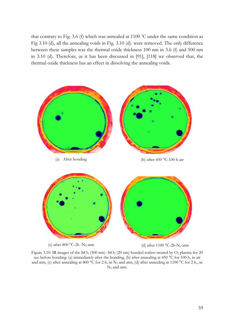
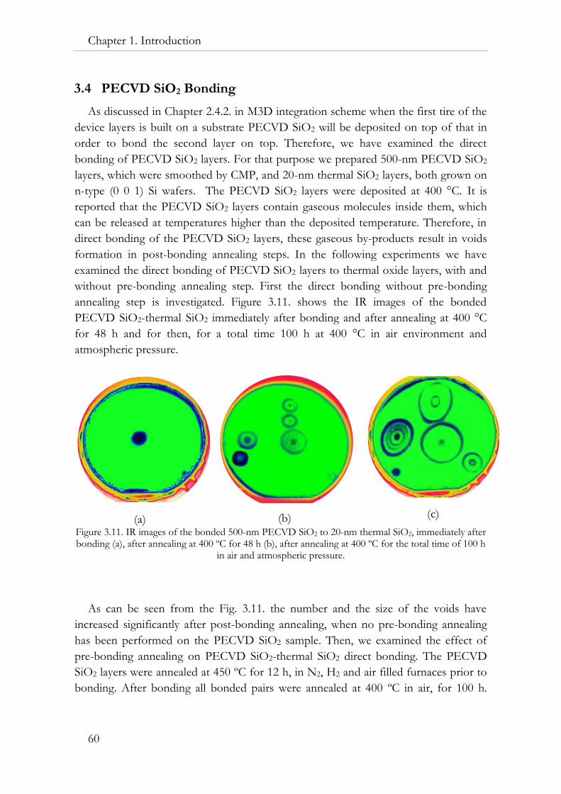


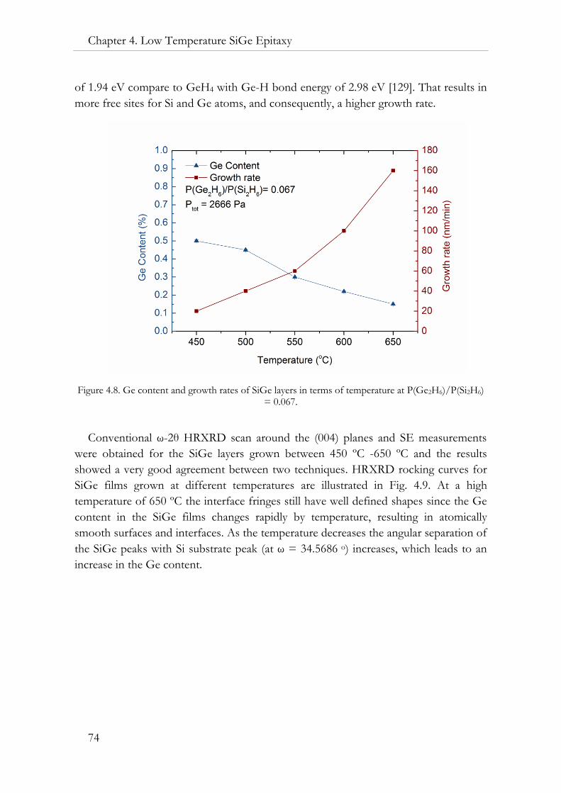


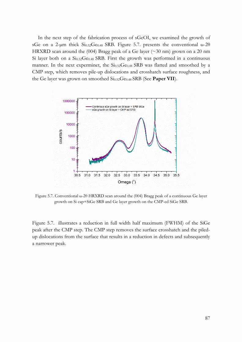


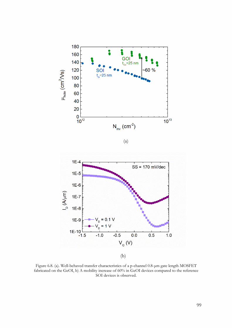


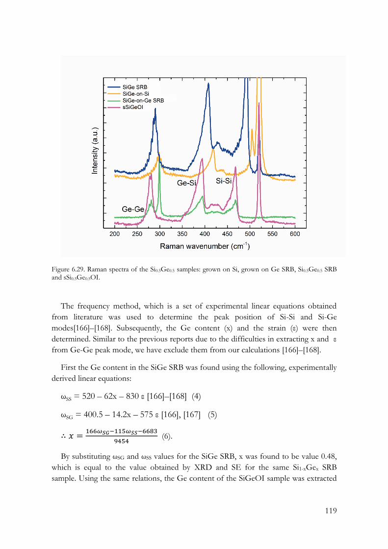


![semiconductors fundamentals.ppt [相容模式] · 2009-02-17 · semiconductors 1. Intrinsic semiconductor is an insulator 2. The conduction property of the SC is determined by the](https://static.documents.pub/doc/80x56/5e79064bb10f26248b3fc636/semiconductors-c-2009-02-17-semiconductors-1-intrinsic-semiconductor.jpg)


![PHYSICS AND MATHEMATICS No', m · Superconductivity 41 - a - [III - USSR - 21 H S & T] Crystals and Semiconductors USSR UDC 621.382.2:535.376 MONOLITHIC LIGHT EMITTING DIODES ON EPITAXIAL](https://static.documents.pub/doc/80x56/608a8b8f16eb474d083c1d09/physics-and-mathematics-no-m-superconductivity-41-a-iii-ussr-21-h-s-.jpg)


