Page 1
Fabrication of Ridge Waveguides
in Lithium Niobate
ASHRAF MOHAMEDELHASSAN
Master of Science Thesis
Stockholm, Sweden 2012
LiNbO3
LiNbO3
PELN
PELN
PELN
PR Mask
PR Mask
Plasma
RIE
Waveguides
y
z
x
LiNbO3
Page 2
Royal Institute of Technology
KTH
Fabrication of Ridge Waveguides in Lithium
Niobate
Ashraf Mohamedelhassan
Master of Science Thesis
Laser Physics
Department of Applied Physics
School of Engineering Science
KTH
Stockholm, Sweden 2012
Page 3
ii
AlbaNova University Center
Royal Institute of Technology KTH
Applied physics department
Laser physics
SE - 106 91 Stockholm
Cover photo:
Top: Sample before (upper) and after (right) the etching process and after removing the photoresist
mask (lower).
Bottom: AFM pictures of tapping mode scanning of C-LN waveguide (Height, amplitude and phase
signal respectively).
TRITA-FYS 2012:14
ISSN: 0280-316X
ISRN: KTH/FYS/--12:14--SE
Printed by Universitetsservice US AB, Stockholm 2012
Page 4
iii
CONTENTS
Chapter1. Introduction…………………………………………………………....1
1.1 Background ……………………......………………………………………...…1
1.2 The aim of the thesis………..………………….………...……………..……....2
1.3 Outline of the thesis………………………..………………………..………….3
1.4 References…….…...……………………………………………………….…...4
Chapter 2. Ridges waveguides in LiNbO3………...…………………..….…...…5
2.1 waveguides geometries..….………..…………..……………………………….5
2.2 Waveguides fabrication techniques …………...…………………..……..….....6
2.3 Waveguides...………...………..………………….……………………………8
2.4 Prism coupled method……………………………...…………...……..………12
2.5 Guided mode descriptions………………………………………………….….13
2.6 References……………………...……………………………………………...15
Chapter 3. Lithium niobate………………………….………………….……......16
3.1 Introduction…………………………………………………………….…...…16
3.2 The crystal growth……………………………………………………….…….16
3.3 LiNbO3 crystal structure……….………….…………………………….….….18
3.4 Photorefractive effect in LiNbO3 ………………………………………….….21
3.5 Optical transmission and refractive indices……………...…………….……...21
3.6 References……………………………………………………………………..24
Chapter 4. Fabrication of PE:LN ridges waveguides……………...………......25
4.1 Introduction…………………………………………………………………....25
4.2 The fabrication steps…………………...……………………………………...25
4.3 Preparation of samples……………………………………………………...…27
4.4 Proton exchange (PE)…………………………………………………........….28
4.5 Photolithography…………………………………………......…….….……....32
4.6 The reactive ion etching………………...………………………….……....….35
4.6.1 The etching mechanism…………………………………...…….……..…….36
4.6.2 Anisotropy plasma etching……..……………………………….……...……38
4.6.3 The etching process in LiNbO3………………..………..…………..…….....39
4.6.4 The etch selectivity……………………..…………………………..…….….40
Page 5
iv
4.6.5 Pressure effect…………………………………………………..…...….…...41
4.6.6 Effect of Radio frequency and ICP powers ….…..……………………..…..41
4.6.7 Etching rate and the etchants gases………………………………..…….…..43
4.6.8 Temperature effect…………………………………………………….…….45
4.6.9 Final recipe……..……………………………………………….…………...45
4.6.10 Waveguides fabrication……………………………………….……………46
4.7 Ridges waveguides ……………...……...………………..……….…..……….51
4.8 Summary of fabrication……………...……………………………….…....…..52
4.9 References …………………………………………………………………….54
Chapter 5. Conclusion, further work and future developments…….…….…..56
5.1 Summary………………………………………………………….…….....…..56
5.2 Further work……………………………………………………….…...……...56
5.3 Future developments………………………………….…………..…….....…..57
5.3 References………………………………………………….…...……....……..58
Page 6
v
ACKNOWLEDGMENT
It gives me great pleasure in acknowledging the support and help of my supervisor Dr.
Katia Gallo, a unique and amazing supervisor. Thanks for teaching, discussing, and for your
guiding and supports. No words can explain and express my deep owes thanks, Katia I am very
thankful, what a great scientist you are!
Many deep thanks to Michele Manzo, my master thesis co-supervisor, I am really
grateful, for the nice time, discussing in the office, and working at the clean room exploring and
learning new things.
I wish to thank, Professor Fredrik Laurell for letting me to do my master thesis project
with his group. I consider it as an honor to work with his group. And it’s my pleasure to work
with Fredrik Laurell, taking from his great knowledge as one of pioneer leader in
Microstucturing LiNbO3. I would like to thanks prof. Valdas Pasiskevicius for sharing
knowledge, for his easy and intelligent way of thinking. Many thanks for Prof. Lars-Gunnar
Andersson for his support, always asking about my project progresses and advising, thank for
Prof. Jens A. Tellefsen and Dr. Carlota Canalias for their warm welcome, also I would like to
thanks Dr. Michael Fokine very much for his support and for the time answering my questions,
advising, share experience, for the time listening to my complaining when I need someone to
talk about my study, future, and my life difficulties, and for the coffee when we work over night,
deep owes thanks Michael. And I will not forget our group member Dr. Mårten Stjernström for a
nice memory. I would like to thank a lot Dr. Marina Zelenina and Dr. Aman Russom, from cell
physics group, for their supports and advising during my study.
I cannot find words to express my gratitude to all nice members of laser physics group
for their welcome, and I would like to give a special thanks to my close contact, my office mates
Charlotte Liljestrand, Hanna Al-Maawali, Michele Manzo and Staffan Tjörnhammar. Many
special thanks to Hoon Jang and Andrius Zukauskas for the nice time discussing physics, sharing
experiences, advising and for their real brotherhood. Many thanks to Dr. Zangwei Yu and Dr.
Daniel Ljunggren for let me sheared their office when I started. Also I am indebted to the clean
room users, from applied physics department and others departments, for high sprit and gentle
manners, specifically to Prof. David Haviland, head of Nanostructure group and Albanova
Nanofabrication laboratory, to Dr. Anders Liljeborg the clean room manager for advising and
guiding, many thanks to Dr. Anders Holmberg and Dr.Tomas Frisk, for helping always, to Stella
Tagliati, for her help, I am really thanks to all of you for the time discussing physics, Micro and
nanostructure processing, I would like to thanks very much Julia Reinspach from Biomedical &
X-ray physics for sharing knowledge, experiences, for help, answer my questions, discussing
Page 7
vi
physics and always have time even when she was so busy doing her research, thanks for you
Julia.
It is with immense gratitude that I acknowledge the support and help of Prof. Kjell
Carlsson, Applied physics master program coordinator, for his care about my study and my life
in Stockholm, for his great advice, direct us how to deal with physics and for his nice talking
introduce to me the Swedish culture when any festivals or certain occasion come, again and
again thanks a lot Kjell Carlsson. Many thanks to Prof. Göran Manneberg for teaching and warm
welcome. Also I am really indebted to Prof. Hans Hertz, the head of applied physics department,
for his support, guiding and advising. My gratitude to all my classmates at Royal Institute of
Technology, for the time revision our lessons, solving exercises and sharing knowledge, stood
beside me in hardness and sharing the happiest times, special thanks to Ida Iranmanesh, and to
my class fellows A. Afridi and R. Bokhari.
I am indebted to my many colleagues who supported me and always asking about me
and send their best hopes and wishes. My deep thanks to my professors and friends at faculty of
Science university of Khartoum, special thanks to Prof. Omer Eid for his support and guidance.
And I am very grateful to all Sudanese in Stockholm for real home atmosphere in abroad. Also I
will not forget to thanks Kristian Neovius, not only home neighbor but also a Swedish brother,
and M. Alhalab my Sudanese brother at Stockholm for their real brotherhood feeling.
I really owe my deepest gratitude to my mother, my first teacher in my life, I would like to
take this opportunity to send her my love, I love you forever ! Also I cannot find words to
express my great gratitude to my father the one who always give me a lot and encourage me to
go ahead in my life and education. I share the credit of my work with my lovely sisters the
flowers that refresh my world, my brothers, and my kind aunts. At last it gives me great pleasure
in acknowledging the support of Rihab the moon of my life, sweet, beauty, and honey wife.
Ashraf, Stockholm January 2012
Page 8
vii
ABSTRACT
Lithium Niobate (LiNbO3) is an artificial negative uniaxial, non-centrosymmetric,
ferroelectric crystal that has a large pyroelectric, piezoelectric, nonlinear and electro-optic
coefficients. LiNbO3 is also a widely used material for hosting optical integrated devices.
The main goal of this thesis has been to develop a reliable technological process to fabricate
ridge waveguides in LiNbO3 by means of reactive ion etching. Ridge waveguides are particularly
promising due to their capability to achieve a strong confinement of light in comparison with
traditional (e.g. indiffused) waveguides, yet their fabrication poses several technological
challenges.
The main challenge to be faced comes from the fact that LiNbO3 is a hard and relatively
inert material, hence relatively difficult to etch. In this master thesis I explored a new
technological solution to enhance the etching rate in LiNbO3 which allowed me to develop a dry-
etch process to fabricate the ridges with standard photo-resist masks.
Ridge waveguides were made on both –Z and +Z, undoped and MgO-doped congruent
LiNbO3 substrates, achieving etching depths of about 500 nm and 300 nm on undoped and MgO-
doped materials, respectively. Further characterizations on the ridge profiles were also
performed by Atomic Force Microscopy techniques.
Page 10
Fabrication of ridge waveguides in Lithium niobate
1
1. Introduction
1.1 Background
Optical waveguides are key component allowing confining and guiding light in
optical integrated circuits (OIC). Using microstructuring techniques is a basic way to
construct devices that deal with controlling and processing light in OIC. The ability to
microstructure specific materials is associated to the selectivity in removing or modify-
ing the material over small scales.
Lithium niobate (LiNbO3, LN) is one of the most used materials for hosting
OIC devices. LiNbO3 is a synthetic dielectric material that does not exist in nature.
Historically it was first discovered in 1949 [1], but the growth as a single crystals was
achieved in 1965 [2]. It shows extremely high nonlinear optical coefficients [3], which
makes it the favorite candidate for realization of optical devices such as parametric
oscillators, parametric amplifiers, second harmonic generators, modulators, etc. Many
different techniques have been employed so far for structuring lithium niobate and
making optical waveguides in it [4, 5, 6, 7].
This master thesis deals with the development at KTH of suitable
microstructuring techniques, (based on photolithography [8] and reactive ion etching [9])
to fabricate ridge waveguides in LiNbO3. The ridge geometry is particularly appealing
due to its capability to achieve a strong confinement of the guided light in comparison
with other waveguide structures [8].
The main challenge to face in the fabrication of ridge waveguides in lithium
niobate comes from the low etching rate of the material and the difficulty to find suitable
masks, with high enough selectivity to allow a deep (> 100 nm) etching. The solution I
have used in my work was to use proton exchange (PE) to weaken the LiNbO3 surface
structure, so to enhance the etching. At same time, the increase in the refractive index
associated with the PE process was used to confine the electromagnetic waves within the
ridge [10].
Both undoped and MgO-doped congruent lithium niobate substrates were used
to fabricate the ridge waveguides. (In this master thesis I shall present the whole fabrica-
Page 11
Fabrication of ridge waveguides in Lithium niobate
2
tion process that I have developed for this purpose at KTH, during my work in the Laser
Physics group at the Applied Physics department.)
1.2 The aim of the thesis
The aim of this thesis is to fabricate ridge waveguides in LiNbO3, with an as
simple as possible fabrication methodology, to achieve high confinement waveguides
which could then be further optimised in combination with periodically poled LiNbO3
(PPLN) structures for integrated nonlinear optical devices.
To achieve this main purpose, I used standard microfabrication techniques, in
particular photolithography techniques, which are simple, cheap, and give high resolu-
tions over large areas, in combination with reactive ion etching (RIE) techniques I built
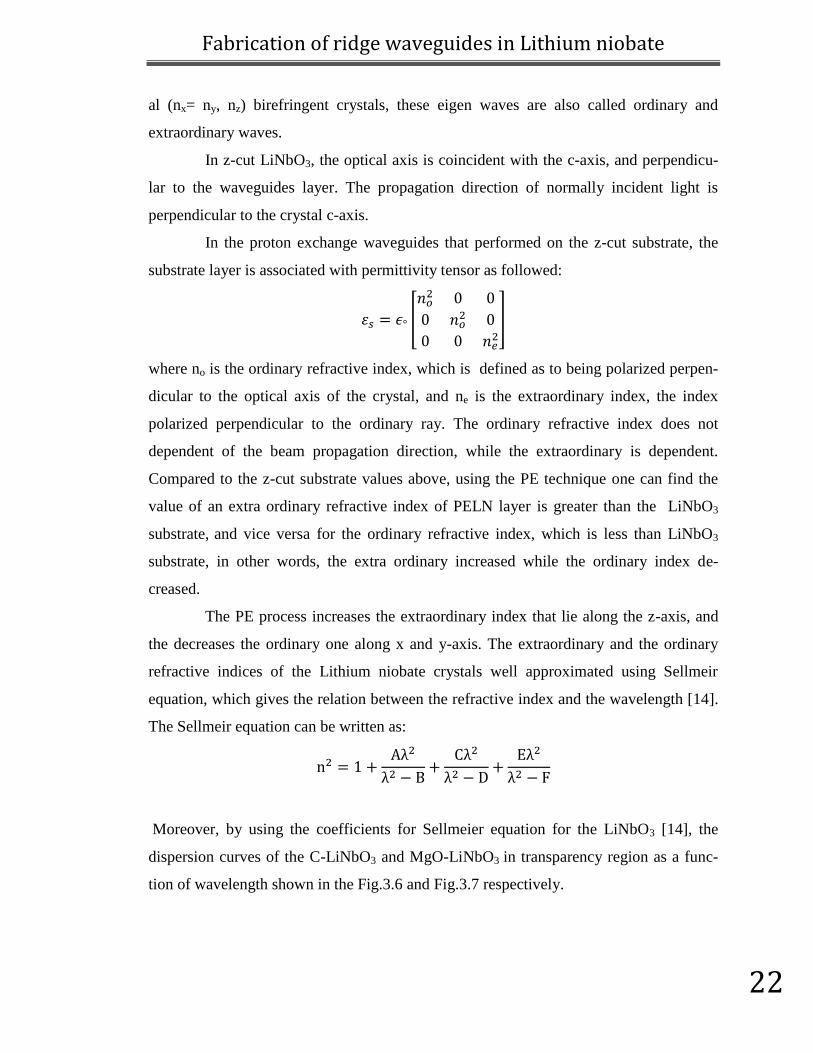
consist of etched PELN ridges, as shown in Fig.1. below, in which the core guiding
region is made of a high refractive index PE layer (nPELN~2.3) embedded on top of the
LN substrate (nLN~2.2) and surrounded on both sides and on the top by air (nAir ~1),
providing a high refractive –index step, to enhance field confinement.
LiNbO3 (
PELN (
y
z
x
Air
Fig.1.1 Structure of PELN ridge waveguides structures fabricated in this thesis.
Page 12
Fabrication of ridge waveguides in Lithium niobate
3
1.3 Outline of Thesis
This thesis can be divided into two parts:
Part I gives a general introduction on waveguides and LiNbO3. There I shall
discuss the fabrication techniques that commonly used to fabricate waveguides in LN,
specifically ion beam implantation [5] and two types of ion diffusion, namely Titanium
indiffusion [6] and the proton exchange [7]. I shall also provide a description of the
proton exchange guiding layer and of the main principle of operation of waveguides, i.e.
total internal reflection. Furthermore, I shall introduce the solutions of Maxwell’s
equations, which describe the electromagnetic field propagation and the modes guided
through the confinement layer of waveguides. In chapter 3, I shall provide a brief
introduction to lithium niobate (i.e. the growth techniques, crystal structure, etc.) and to
undoped and MgO-doped substrates.
Part II is the fabrication part, containing all the details and discussions on the
microstructuring techniques that used and developed in my work. It is the core of the
thesis work. It contains the details of the proton exchange process, and the conditions
used for the ridges. The photolithographic techniques that I used to pattern the ridges are
presented in chapter 4, where I give a detailed description of my reactive ion etching
studies. To give an idea of what the reactive ion etching actually does, a description of
the RIE chamber setup and how to ignite the plasma are also included. I also introduce
the basics of the etching mechanisms, in particular the sputtering, chemical etch, and
ion-assisted etching, which have to be used synergetically in order to achieve an aniso-
tropic etching. This chapter presents also a discussion of the parameters I used to
optimize the etching process. The results of the recipe that I used finally chose to etch
the ridges are then reported, including a study of their roughness made with the atomic
force microscope (AFM) facilities of the Albanova Nanofabrication lab.
At the end of the thesis, in chapter 5, a summary of the work and discussions
for further developments are reported.
Page 13
Fabrication of ridge waveguides in Lithium niobate
4
1.4 References
[1] B.T. Matthias, J. P. Rameika, “Ferroelctricity in the ilmenite structure”, Phys.
Rev, 76, 1886 (1949).
[2] A.A. Ballman,”Growth of piezoelectric and ferroelectric materials by
Czochralski technique”, J.Am.Ceram.Soc, 48, 112 (1965).
[3] R.S. Weis, T.K. Gaylord, “Lithium niobate: summary of physical properties and
crystal structure”, Applied Phys, 37, 191(1985).
[4] F. Laurell, J. Webjörn, G. Arvidsson, J.Holmberg, ”Wet etching of proton
exchange lithium niobate a novel processing technique”, J. Light wave. Tech-
nology, 10, 1606 (1992).
[5] P.D. Townsend, P.J. Chandler, L. Zhang, “Optical effect of ion implantation”,
Cambridge University Press (1994).
[6] W.K. Burns, P.H. Klein, E.J. West, L.E. Plew, ”Ti diffusion in Ti:LiNbO3
planar and channel optical waveguides”, Appl. Phys, 50, 6175(1979).
[7] J.L. Jackel, C.E. Rice, J.J. Veselka,”Proton exchange for high index waveguides
in LiNbO3“, Appl. Phys. Lett, 41, 607 (1982).
[8] H.Nishihara, M.Haruna and T.Suhara, “Optical Integrated Circuits”, McGraw-
Hill (1989).
[9] H. Hu, A.P. Milenin, R.B. Wehrspohn, H. Hermann, and Sohler, “Plasma
etching of proton exchange lithium niobate”, J. Vac. Sci. Technology. A, 24,
1012 (2006).
[10] J.L. Jackel, C.E. Rice, J.J. Veselka, “Proton exchange for high index waveguides
in LiNbO3”, Appl. Phys. Lett, 41, 607 (1982).
Page 14
Fabrication of ridge waveguides in Lithium niobate
5
2. Ridge waveguides in LiNbO3
2.1 Waveguides geometries
The basic picture of a planar (2D) waveguide is shown in Fig.2.1. It consists of
a sandwich of three layers called cladding, film, and substrate layer, of refractive indices
nc, nf, and ns respectively. The condition to be fulfilled for the light to be confined in the
guided layer by total internal reflection is nc< ns< nf, with a required thickness value T
for the film layer, called the critical thickness [1]. The picture also illustrates the princi-
ple of operation of the waveguide, namely total internal reflection: when a ray of light
propagating in the high index region (nf) hits the interface with a medium of a lower
refractive index (nc or ns) at an angle larger than the critical angle, there is no light that
can cross the interface, so that the beam is trapped in the guiding layer.
In the planar waveguide, light confinement takes place only in one direction, as
shown in Fig.2.1, where the confinement takes place along z and the propagating along
x, but light can still spread out in the perpendicular direction (y-axis) due to diffraction
[2].
To confine light also in the other transverse direction in addition to the depth (z)
one needs to create a localized high refractive index region also along y. In this way, by
patterning the refractive index profile in 2D (y-z) one can achieve total internal reflec-
tion at the upper and lower interfaces as well as at the surrounding interfaces. This
Fig.2.1Planar optical waveguides
Page 15
Fabrication of ridge waveguides in Lithium niobate
6
corresponds to making a channel waveguide, which avoids light spreading and keeps all
the light well confined in both transverse directions.
A channel ridge waveguide structure can be achieved if one by some means
succeeds in removing the outer cladding layer film from a planar (2D) waveguide as
shown in Fig.2.1, while leaving the waveguide film layer in the central portion intact,
with a depth high enough to sustain guidance, as shown in Fig.2.2 (a). In comparison to
standard embedded channels made by,e.g. ion exchange (see Fig.2.2 (b)) the ridge
structures can allow to a much stronger confinement by achieving a high refractive index
step. For instance considering the case of PELN channel waveguides, one could achieve
an index step ~0.12 at best in the lateral direction (y in Fig.2.2b), while for the same
direction a PELN ridge yields an index increase of ~1.2 (due to the high index step
between LN and air).
2.2 Waveguide fabrication techniques
Many techniques are used to fabricate waveguides in LiNbO3, such as ion/metal
diffusion (e.g. titanium indiffusion [3] [4] or the proton exchange [5]) and ion beam
implantation [6].
The Titanium indiffusion process consists in depositing a Titanium layer on the
surface of a substrate and then thermally indiffusing it into the crystalline substrate by
baking at a temperature ~ 1000oC. This increases the refractive index in the diffusion
areas by ~0.001 [3]. Waveguides made by Ti diffusion suffer from increased photore-
fractive damage, which means that the devices cannot operate at very high power
Fig.2.2 (a) Ridge and (b) Buried waveguides structures.
Page 16
Fabrication of ridge waveguides in Lithium niobate
7
densities in the visible [3]. Furthermore, the high processing temperatures complicate the
fabrication steps to combine Ti:waveguides with PPLN.
Proton exchange (PE) is one of the most popular methods to fabricate waveguides.
It consists in an ion exchange process taking place at the crystal surface, where lithium
ions in LiNbO3 are substituted by protons (H+) coming from an acidic melt solution. In
contrast with Ti:diffusion, which yields waveguides guiding all polarizations in LN, PE
waveguides can only guide light of extraordinary polarization, i.e. light polarized along
the crystal optical axis (z, see section 3.5)
Ion beam implantation (IBI) is a process that changes the properties of a materi-
al by forcefully embedding in it different types of ions. It typically gives a negative
index change in a buried region where the bombarding ions stop in the crystal. IBI is
suitable for materials that can have major changes in their properties caused by a small
number of implanted particles, typically N+, B
+, He
+ and Ne
+ [7]. IBI has been applied to
make waveguides in LiNbO3 [3], but it typically causes damage to the ion-bombarded
layer below the surface After the process the samples must be annealed to heal the
surface damage [3], but that is not always enough to bring the waveguide losses down to
values acceptable for high-quality devices. In addition, it was reported that the ion beam
implantation can affect negatively the surface properties, e.g. by increasing the hardness
and resistance to oxidation [3].
Another way to fabricate channel waveguides in LiNbO3, is to make ridges by
purely chemical (wet) etching, but there are a few drawbacks with that, associated to the
isotropic nature of the etch, which results from the fact that the chemical etching works
essentially in all directions. HF solutions are typically used to etch LiNbO3 according to
the following chemical reaction
It has been reported that, the chemical reaction has fast etching rate along –Z axis than
the +Z one [8] [9], this is due to the spontaneous polarization of the ferroelectric sub-
strate, which can make the reactions work at different speeds on the two Z faces, due to
the embedded electric field at the surfaces which can either enhance or work against the
protonization process. What happens actually in the wet chemical process is that the
hydrogen ions in the acidic solution react with oxygen ions at the crystal surface forming
Page 17
Fabrication of ridge waveguides in Lithium niobate
8
water, and then the fluorine and niobium ions get attached and are removed from the
crystal. Then a cycled protonization process takes place letting the Li dissolve into the
solution. One way to etch the +Z face is to destroy partially the depolarization field, e.g.
by using the proton exchange process.
Nowadays one of the preferred ways to microstructure lithium niobate is to use
the dry plasma etching techniques [11] see Fig.2.3 above. This process is a good way to
avoid the isotropic processes occurring during chemical wet etching.
In this work, we demonstrate how one can effectively use proton exchange pro-
cess to significantly enhance the dry etching rates in LiNbO3and make ridge waveguides
with a simple photoresist mask.
The ridges waveguides I fabricated were made from proton exchange layers lo-
cated on top of the surface of the LiNbO3 substrates forming a high refractive index film.
The core guiding and confinement region was then patterned by etching, and consisted
in a PELN core surrounded by air in the upper layer and on the sides, and having the
lithium niobate substrate at the lower interface. The etching structures I made are of the
type described by Fig.2.2(b) (rib-waveguides), where the PE layer is not etched all the
way through, yet the ridges are high enough to still guarantee the bi-dimensional con-
finement of light in the transverse plane.
2.3 Waveguides
Waveguides can confine and guide the light by a series of total internal reflec-
tions. To explain this, suppose that we have a high refractive index region (PELN)
working as waveguide layer, lying over a LiNbO3 substrate, and surrounded by air which
working as the cladding layer. According to Snell’s law, any incident ray of light that
forms an angle with the normal to the interface can be trapped in the PELN layer
Fig.2.3 ICP plasma etching structure in
LiNbO3 [10].
Page 18
Fabrication of ridge waveguides in Lithium niobate
9
through a series of total internal reflections (TIR), when Ө is higher than the critical
angles for TIR at the upper (Өf ) and lower (Өs) interfaces, which amount to:
2.1
2.2
Since n(LN) ˃ n(Air), then Өf < Өs. This implies three possible ranges for the angle ,
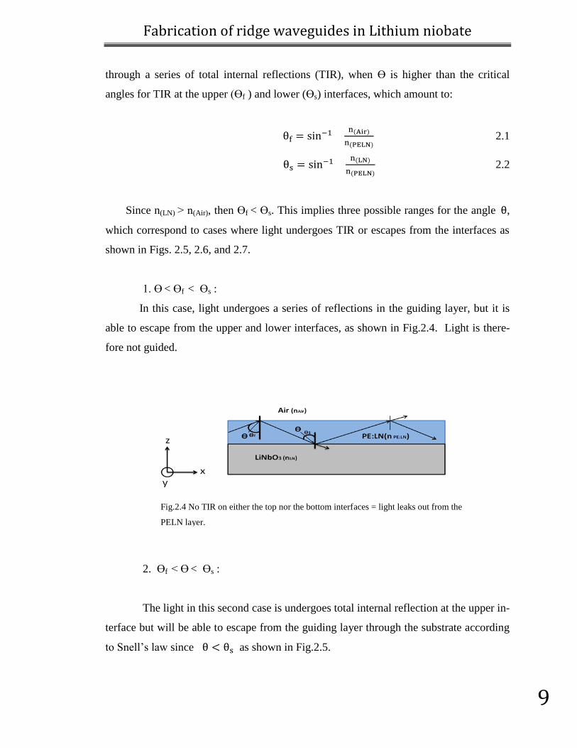
which correspond to cases where light undergoes TIR or escapes from the interfaces as
shown in Figs. 2.5, 2.6, and 2.7.
1. Ө < Өf < Өs :
In this case, light undergoes a series of reflections in the guiding layer, but it is
able to escape from the upper and lower interfaces, as shown in Fig.2.4. Light is there-
fore not guided.
2. Өf < Ө < Өs :
The light in this second case is undergoes total internal reflection at the upper in-
terface but will be able to escape from the guiding layer through the substrate according
to Snell’s law since as shown in Fig.2.5.
Fig.2.4 No TIR on either the top nor the bottom interfaces = light leaks out from the
PELN layer.
Page 19
Fabrication of ridge waveguides in Lithium niobate
10
3. Өs < Ө <
:
This third case corresponds to guidance. As shown in Fig. 2.6 the is light con-
fined in the guiding layer, as it undergoes total internal reflections at both the upper and
the lower interfaces and propagates in a zigzag path along x.
The condition to confine light in the PELN layer is then
2.3
By multiply the sin function to 2.3 we get:
2.4
Fig.2.6 Total internal reflection at both top and bottom interfaces corresponds to guidance inside the
PELN layer.
Fig.2.5 Total internal reflection at the top of the PELN layer with radiation
escaping at lower interface.
Page 20
Fabrication of ridge waveguides in Lithium niobate
11
Using the equation 2.2, this gives
2.5
2.6
The value is called the effective index of the guided mode. In the
more general case of a graded index waveguide, the effective indices of its guided modes
can be calculated, for a given refractive index distribution n = n (z), as the solutions of
an eigenvalue equations (see ref. [1] for more details). So far, we have considered planar
waveguides. In a ridge waveguide, light is confined also in the other transverse direction,
i.e. y (if we were to follow the notation of in Fig. 2.7, where x is the propagation direc-
tion in the waveguide).
To calculate the effective indices of the guided modes in a ridge wave-
guide, one can use the simplified treatment of effective index theory [1], an analytical
method applicable to waveguide with 2D confinement. The waveguide is decomposed
into three regions (RI, RII and RI), which are treated as three asymmetric planar wave-
guides, in the x direction, having three different effective indices, neff (RI), neff (RII), and
neff (RI) see Fig.2.7 (a) below.
Fig.2.7 The effective index method applied to ridge waveguides.
Page 21
Fabrication of ridge waveguides in Lithium niobate
12
The guided modes can be determined by finding the effective index vertically for the
regions (RI) and (RII) see Fig.2.7 (a), which they have PELN layers thicknesses (d1) and
(d2) respectively. Then the ridge waveguides effective index (neff) can be calculated by
solving horizontally the eigenvalue problem for a simple symmetric planar waveguides
lied along y direction, see Fig.2.7. (b), having a cover layer with neff (RI), waveguides
layer with thickness (w) an effective index neff (RII), and substrate with effective index
neff (RI).
2.4 Prism coupled method
The reduced thickness of thin film waveguides requires specific techniques for
light coupling. The prism coupler is a way to couple the light into the waveguides,
illustrated in Fig. 2.8. Light can be coupled into a planar waveguide via a high-refractive
index prism attached on its surface. is the incidence angle of light from the prism into
the waveguides, is the prism base angle and alpha is the external incidence angle into
the prism. d is the thickness of the waveguides layer (PELN).
The light beam that goes into the prism will undergo total internal reflection at
the prism base, unless the prism and waveguide are brought into such a close contact that
tunneling across the intermediate air layer can occur. Then the waves in the prism and in
the waveguide can be coupled through their evanescent fields when the projection along
the waveguide axis of the propagation wave vector of light in the prism equals the
propagation vector of a guided mode in the PELN layer.
Fig.2.8 Sketch illustrating prism coupling on a PELN planar waveguide.
x
y
z
Page 22
Fabrication of ridge waveguides in Lithium niobate
13
2.5 Guided modes descriptions
Ridge PELN waveguides allows us to guides the transverse electric (TE) mode
in the x and y-cut substrates while the transverse magnetic (TM) mode in the z-cut
substrate only (Which gives a property to the access to control the polarization in optical
devices).
In this work, the ridges were fabricated along x, as a propagation direction,
thus transverse magnetic field polarized along y-axis and electric field mainly polarized
along z-axis this and due to the PE only light of extraordinary polarization allow to be
guided in ridges PELN waveguides using z-cut substrate.
The equations describing propagating of an electromagnetic harmonic wave at
frequency propagating along the x-axis direction of a planar PELN waveguide as in
Fig.2.6, assuming lossless (zero conductivity), and non-magnetic materials (permeability
µ=µo) can be written in the form:
2.10
Where E and H are the electric and magnetic fields respectively, is the mode propaga-
tion constant, the angular frequency c λ, c is the light velocity in vacuum
, and and
are the dielectric permittivity and magnetic permeability of free
space, respectively.
Suppose that the medium is isotropic and linear ( . Then by using the Maxwell’s
curl equations below we have:
2.11
2.12
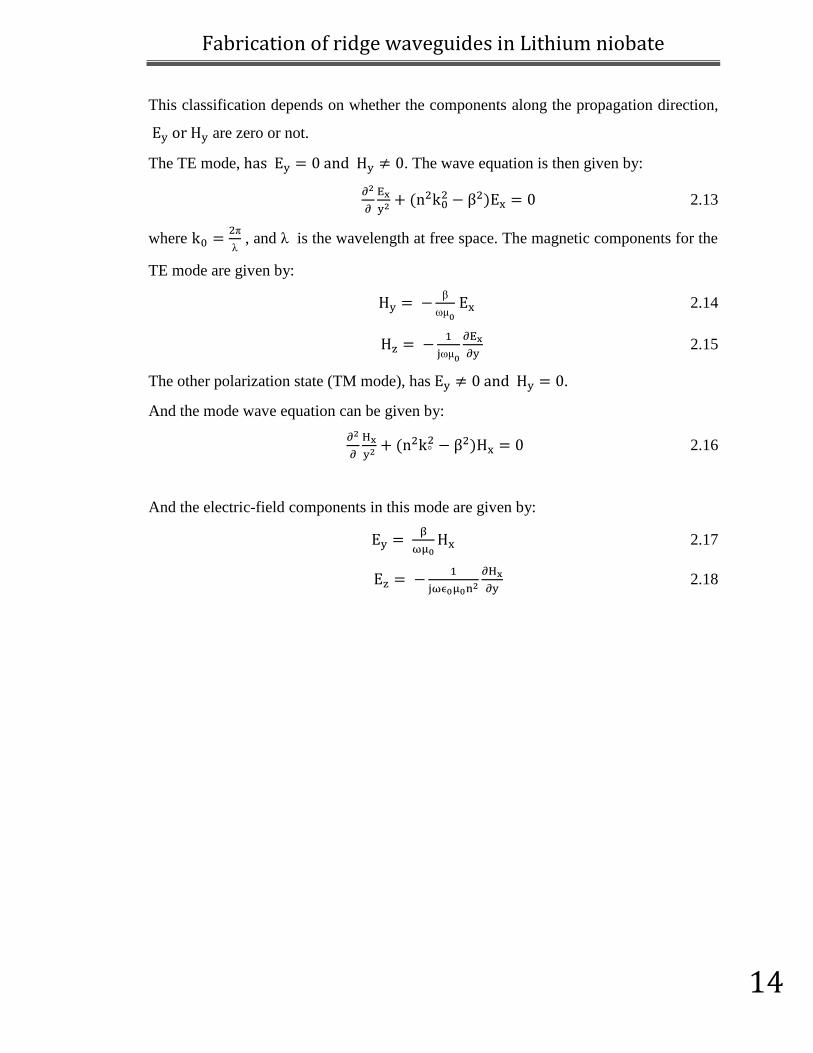
In a planar waveguide, the electromagnetic field can be classified in two
different modes with mutually orthogonal polarization states [1]. One is the TE mode,
which consists of the field components , and the other is the TM mode,
which has the field components .
Page 23
Fabrication of ridge waveguides in Lithium niobate
14
This classification depends on whether the components along the propagation direction,
are zero or not.
The TE mode, . The wave equation is then given by:
2.13
where
λ , and λ is the wavelength at free space. The magnetic components for the
TE mode are given by:
2.14
2.15
The other polarization state (TM mode), has .
And the mode wave equation can be given by:
2.16
And the electric-field components in this mode are given by:
2.17
2.18
Page 24
Fabrication of ridge waveguides in Lithium niobate
15
2.6 References
[1] H.Nishihara, M.Haruna and T.Suhara, “Optical Integrated Circuits”, McGraw-Hill
(1989).
[2] G. Lifante,” Intergraded photonics fundamentals”, John Wiley and sons Ltd,
(2003).
[3] W.K. Burns, P.H. Klein, E.J. West, L.E. Plew, “Ti diffusion in Ti:LiNbO3 planar
and channel optical waveguides”, Appl. Phys, 50, 6175 (1979).
[4] W. S. Yang, H.-Y. Lee, W.K. Kim, D.H.Yoon, “Asymmetry ridge structure fabrica-
tion and reactive ion etching of LiNbO3”, Optical materials, 27, 1642 (2005).
[5] J.L. Jackel, C.E. Rice, J.J. Veselka,”Proton exchange for high index waveguides in
LiNbO3”, Appl. Phys. Lett, 41, 607 (1982).
[6] P.D. Townsend, P.J. Chandler, L. Zhang, “Optical effect of ion implantation”,
Cambridge University Press (1994).
[7] Yu.N. Korkishko and V.A. Fedorov, “Ion exchange in single crystals for Integrated
optics and optoelectronics”, Cambridge international science Publishing (1999).
[8] F. Laurell, J. Webjörn, G. Arvidsson, J.Holmberg, ” Wet etching of proton ex-
change Lithium niobate a novel processing technique”, J. Light wave.Technology,
10, 1606 (1992).
[9] H.Hu, R. Ricken, W. Sohler, and R.B. Wehrspohn, “Lithium niobate ridge wave-
guides fabricated by wet etching”, IEEE PHOTON TECHN LETT, 19, 6 (2007).
[10] H. Hu, R. Ricken and W. Sohler, ” Etching of Lithium niobate: form ridge wave-
guides to photonic crystal structures”, Eindhoven, The Netherlands (2008).
[11] H.Hu, A.P. Milenin, R.B. Wehrspohn, H. Hermann, and Sohler, “Plasma etching of
proton exchange lithium niobate”, J. Vac. Sci. Technol. A, 24, 1012 (2006).
Page 25
Fabrication of ridge waveguides in Lithium niobate
16
3. Lithium niobate
3.1 Introduction
Lithium Niobate (LiNbO3, LN), is an artificial, negative, uniaxial, non-
centrosymmetric, ferroelectric crystal. For its manifold properties, LiNbO3 is a widely
used crystal in different fields of science and technology. As matter of fact, LiNbO3 is
characterised by large pyroelectric, piezoelectric, nonlinear and electro-optic coefficients
and it is also employed for applications in which acoustic and acousto-optic properties
are required.
3.2 Crystal growth
LiNbO3 does not exist in nature. The preferred method to growth this crystal is
the Czochralski technique. Fig.3.1(a) shows the typical setup employed in this method.
LiNbO3 is grown from pure powders of lithium carbonate (Li2CO3) and niobium
pentoxide (Nb2O5) that are melted in a platinum crucible. The following chemical
reaction regulates the crystal growth:
The reaction occurs in the platinum crucible that is placed inside a furnace. The reactants
are heated to the melting point, and then they kept in the liquid phase. Then a seed
attached to the end of a pull rod is brought close to the melt surface, and heated to a
temperature near the melting point of LiNbO3 (1250 [1]. After that, the pulling rod is
lowered to get into contact with the melt surface, so that the reaction at the solid – liquid
interface takes place. At the right temperature, just above the melting point of LiNbO3,
atoms from the liquid will adhere to the seed. At higher temperatures, the seed melts
while on the contrary at lower temperatures the melt freezes locally around the seed.
During the growth of the crystal, the rod is kept in rotation in order to guarantee homo-
geneity and to avoid thermal gradients in the crystal.
Page 26
Fabrication of ridge waveguides in Lithium niobate
17
The diameter of the crystal boule is kept constant during the growth until the
desired length is reached. The control of boule dimensions is achieved by setting the
choosing the diameter of the crucible, the rotation and the pulling rate. The crystal is
finally separate from the melt by increasing the temperature and raising the rod. After
the separation, the growth chamber is cooled down to room temperature. The crystal is
then cut and polished.
LiNbO3 can be grown in a wide range of compositions. The composition ex-
actly matching the chemical compound LiNbO3, having a ratio of [Li]:[Nb]:[O] of 1:1:3
is commonly referred as Stoichiometric Lithium Niobate (SLN). However, due to the
volatility of the Li ions and their consequent deficiency in the crystal, the growth of the
stoichiometric composition is quite challenging. The composition that is easiest to grow
with a good uniformity (and is therefore commonly used) is the congruent one (C-
LiNbO3).
Historically, LiNbO3 has been prepared in both stoichiometric and congruent
composition. The latter is now the preferred one because of its highest optical quality
and uniformity. Fig.3.2 shows the phase diagram for LiNbO3. There is a unique point
called congruent point, at which both the solid and the liquid phase can co-exist and it
corresponds to the highest point on the melting temperature line. The ratio of Li to the
total Li and Nb concentration is 48, 45% [4] and it has the same molar ratio in the solid
and in the melt crystal. This feature makes it easier to growth this composition with good
a) b)
Fig.3.1 a) Setup view for the growth by using the Czochralski technique [2], b) Single crystal of LiNbO3 [3].
Page 27
Fabrication of ridge waveguides in Lithium niobate
18
homogeneity. Crystals grown in other points of the phase diagram have in general much
greater variation in composition, showing inconsistencies in refractive indices [4].
MgO-LiNbO3 is grown from a melt with Li/Nb ratio equal to that of an undoped
congruent melt with addition of 5 mol% of MgO [6]. MgO, with 5mol% concentration,
has been shown to be a good dopant to improve the resistance to photorefractive damage
and to preserve the large non linear optical coefficient so to make it capable to work at
substantially higher powers [7], moreover it has stable refractive index.
3.3 LiNbO3 crystal structure
LiNbO3 belongs to the perovskite crystal family. The crystal structure consists of
planar sheets of oxygen atoms in a distorted hexagonal close-packed configuration [8]
showed in Fig.3.3. The interstices of the oxygen octahedra are filled one-third by lithium
ions, one-third by niobium and one-third is vacant. In the z direction, the atoms are
placed in the interstices in the following order: Nb, vacancy, Li [9].
The LiNbO3 crystal below the Curie temperature, i.e. in its ferroelectric phase,
exhibits three-fold rotation symmetry about the c-axis, so LiNbO3 is a trigonal crystal.
Fig.3.2 Li2O- Nb2O5 equilibrium temperature –composition phase diagram of LiNbO3 [5].
Page 28
Fabrication of ridge waveguides in Lithium niobate
19
LiNbO3 is a trigonal crystal since it exhibits three-fold rotation symmetry
around the c-axis. It exhibits mirror symmetry of three planes lying 60 apart and
forming a threefold rotation axis, as shown in Fig.3.4. These two symmetries classify
LiNbO3 as a member of the 3m point group it also belongs to the R3c space group [10].
LiNbO3 is ferroelectric below the Curie temperature (1140 C) whereas when
above (but below the melting temperature) the displacement of the Li and Nb ions in
respect to the oxygen planes vanishes and therefore the spontaneous polarization vanish-
es too, then the paralectric phase arises.
The orientation of the c-axis is given by the position of two neighbor lithium
and niobium atoms, as well as of the vacancies with respect to the closed-packed oxygen
planes. The two atoms are displaced slightly away from the octahedra center along c-
axis arising a spontaneous polarization aligned along this axis. These pairs can work as
individual axis and they can be aligned either up or down indicating the domain polari-
zations. The standard methods to determine the c-axis orientation is to compress the
crystalline in the c-axis direction. The c+ face (the positive end of the ferroelectric
dipole) will exhibit a negative charge under compression, when the niobium and the
lithium ions move closer to their paraelectric position, thus reducing the dipole, while
Fig.3.3 Paraelectric (a) and Ferroelectric (b) phase in LN [8].
(b) (a)
Lithium
Niobium
Oxygen
Page 29
Fabrication of ridge waveguides in Lithium niobate
20
the c- face (the negative end of the dipole) exhibits a positive charge under compression
[4].
There are two different unit cells in LiNbO3: hexagonal or rhombohedra. In the
first one, showed in Fig.3.4, the z-axis is chosen to be parallel to the c-axis of the crystal.
The y-axis is chosen to be parallel to one of the mirror plane, and the x-axis chosen so to
form a right-handed system [11]. This conventional hexagonal unit cell contains six
formula weights (147.843 amu). The three equivalents a axis in the conventional hexag-
onal unit cell are 120 degree apart and lie in a plane normal to the c-axis. These axis are
chosen to be perpendicular to the mirror planes (a1and a2 are shown in Fig.3.4). It is
conventional to take in this hexagonal unit cell the Nb as the origin, for the congruent
compounds LiNbO3 unit cell length a, are aH = 5.1536 . While in the other type rhom-
bohedra unit cell, aR 5.474 Ȧ and the angle between these three axis are 56.180
degree [12]
Fig.3.4 LiNbO3 symmetry mirror phase.
Page 30
Fabrication of ridge waveguides in Lithium niobate
21
3.4 Photorefractive effect in LiNbO3
The photorefractive effect is the variation of the refractive index due to optical-
ly generated charge carriers. The photorefractive effect in LiNbO3 is caused by charges
migrations and accumulation due to the photovoltaic effect. Since, LiNbO3 is electro-
optic, the accumulation of charges generate an electric field that locally changes the
refractive index. When a crystal of C-LiNbO3 is illuminated by green or blue light (λ<
~550 nm) electrons from impurities (Fe2+
, Fe3+
) are photo-excited and generate a light-
induced variation of the refractive index. Photorefraction can manifest itself in various
ways like phase modulation, beam break-up, Bragg scattering, reduction of efficiency in
nonlinear interactions, beam distortion, etc [12].
To minimize these effects, one can for instance use to work at higher temperature
or by making the LiNbO3 more stoichiometric, in order to reduce the presence of impuri-
ties which are located in lithium vacancies. Another approach is, as mentioned in 3.2, to
add metal impurities such as Magnesium. The optical damage is then lowered preventing
the build up of the static field that cause the photorefractive effect [12].
3.5 Optical transmission and refractive indices
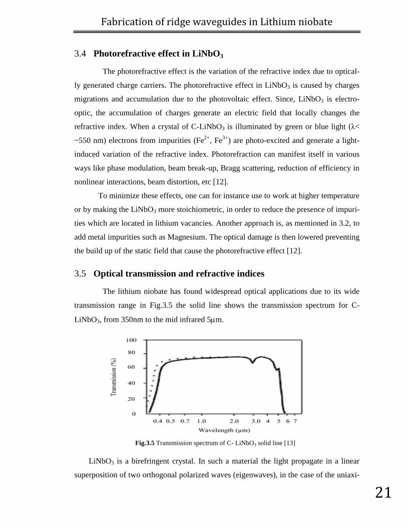
The lithium niobate has found widespread optical applications due to its wide
transmission range in Fig.3.5 the solid line shows the transmission spectrum for C-
LiNbO3, from 350nm to the mid infrared 5m.
LiNbO3 is a birefringent crystal. In such a material the light propagate in a linear
superposition of two orthogonal polarized waves (eigenwaves), in the case of the uniaxi-
Fig.3.5 Transmission spectrum of C- LiNbO3 solid line [13]
Page 31
Fabrication of ridge waveguides in Lithium niobate
22
al (nx= ny, nz) birefringent crystals, these eigen waves are also called ordinary and
extraordinary waves.
In z-cut LiNbO3, the optical axis is coincident with the c-axis, and perpendicu-
lar to the waveguides layer. The propagation direction of normally incident light is
perpendicular to the crystal c-axis.
In the proton exchange waveguides that performed on the z-cut substrate, the
substrate layer is associated with permittivity tensor as followed:
where no is the ordinary refractive index, which is defined as to being polarized perpen-
dicular to the optical axis of the crystal, and ne is the extraordinary index, the index
polarized perpendicular to the ordinary ray. The ordinary refractive index does not
dependent of the beam propagation direction, while the extraordinary is dependent.
Compared to the z-cut substrate values above, using the PE technique one can find the
value of an extra ordinary refractive index of PELN layer is greater than the LiNbO3
substrate, and vice versa for the ordinary refractive index, which is less than LiNbO3
substrate, in other words, the extra ordinary increased while the ordinary index de-
creased.
The PE process increases the extraordinary index that lie along the z-axis, and
the decreases the ordinary one along x and y-axis. The extraordinary and the ordinary
refractive indices of the Lithium niobate crystals well approximated using Sellmeir
equation, which gives the relation between the refractive index and the wavelength [14].
The Sellmeir equation can be written as:
Moreover, by using the coefficients for Sellmeier equation for the LiNbO3 [14], the
dispersion curves of the C-LiNbO3 and MgO-LiNbO3 in transparency region as a func-
tion of wavelength shown in the Fig.3.6 and Fig.3.7 respectively.
Page 32
Fabrication of ridge waveguides in Lithium niobate
23
Fig.3.6 Refractive indices of C-LiNbO3 as functions of wavelength.
Fig.3.7 Refractive indices of MgO-LiNbO3 as functions of wavelength.
0 1 2 3 4 5 61.8
2
2.2
2.4
2.6
2.8
3
Wavelength (µm)
Refr
active index
Refrctive indices of C-LiNbO3
ne
no
0 1 2 3 4 5 61.8
1.9
2
2.1
2.2
2.3
2.4
2.5
2.6
2.7
2.8
Wavelength (µm)
Re
fra
ctive
in
de
x
Refrctive indices of MgO-LiNbO3
ne
no
Page 33
Fabrication of ridge waveguides in Lithium niobate
24
3.6 References
[1] D.H. Jundt and G. Foulon,”Boules of LiNbO3 congruent grown by the Czochralski
technique”, in properties of Lithium niobate (Ed, K.K. Wong) pp.25-27, INSPEC,
London (2002).
[2] B.Q.Li, “Solidification processing of materials in magnetic fields”, JOM- e, 50, 2
(1998). [3] http://www.smm.co.jp/E/business/material/product/lithium/
[4] EMIS Data review series No.5, “Properties of lithium niobate”, INSPEC London
(1989).
[5] G Malovichko, V Grachev, E kokanyan and O Schirmer, “Optimization of lithium
niobate for advanced applications by variation of extrinsic and intrinsic defect
subsystems”, Ferroelectrics 258 ,131 (2001).
[6] D.H. Jundt, M.C.C Kajiyama, D.Djukic, M. Falk, “Optical methods to character-
ize crystal composition of MgO doped lithium neonate”, Journal of crystal growth
312, 1109 (2010).
[7] P. Gunter and J.P.Huignard Ed, “Photorefractive materials and their applications
I”, Topic in Applied Physics, 61, (1988).
[8] R. S. Weis, T.K. Gaylord, “Lithium niobate: summary of physical properties and
crystal structure”, Applied Phys, 37, 191(1985).
[9] S.C. Abrahams, J.M. Reddy, J.L. Bernstein,”FerroelectricLithium niobate III.
Single crystal X-ray studies at 24oC “, J.Chem.Phys. Solids,27, 989(1966)
[10] B. K. Vainshtein, “Symmetry, and Methods of structural Crystallography”,
Springer series in solid-state science, 15 (1981).
[11] IRE Standards on Piezoelectric Crystals, IEEE Standard 176; also. Proc. I R E,
vol. 37, 1378-1395, December (1949).
[8] Yu. N.Korkishko and V.A. Fedorov, “Ion exchange in single crystal for integrated
optics and optoelectronics”, Cambridge international science publishing, England
(1999).
[13] M. Lawrence, “lithium niobate integrated optics”, Rep. Prop. Phys, 363 (1993).
[14] D. Jundt, D.E.Zelmon and D.L small,” Infrared corrected Sellmeier coefficients
for congruently grown lithium niobate and 5mol% magnesium oxide doped
lithium niobate”, J. Op. Am. B, vol.14, No.12, December (1997).
Page 34
Fabrication of ridge waveguides in Lithium niobate
25
4. Fabrication of PE:LN waveguides
4.1 Introduction
Lithium niobate is a hard and relatively inert material, hence relatively difficult
to etch. Standard micromachining technologies, such as laser ablation or, wet acid
etching, are often not suitable for achieving the fine and high-aspect ratio typically
required for optical devices. Specifically, the low-etching rates of lithium niobate make
high-quality etching already challenging for depth of the order of micrometers. With
reactive ion etching (RIE) [1] sub micrometer etching depths have been achieved in
LiNbO3 substrates, by using high-density plasma tools, such as inductive coupled plasma
(ICP), to enhance the etching rate and Chromium masks to maximize selectivity [2].
In this master thesis, I explored a new technological solution to enhance the
etching rate of LiNbO3 in the RIE process using a standard photo-resist mask and I used
it to fabricate 500 nm high PE:LN waveguides. This chapter will provide an overview of
the whole fabrication process I developed for this purpose, at the Albanova nanofabrica-
tion lab at the Applied Physics department.
4.2 The fabrication steps
As discussed in chapter 2, several techniques are available to make waveguides
in lithium niobate, such as titanium in-diffusion [3] [4], and proton exchange (PE) [5].
The proton exchange technique is cheap, simple and implies processing at relatively low
temperatures (~200ºC). Among all diffusion and exchange techniques, PE is the one that
can provide the highest refractive index increase. Indeed, along the crystal optical axis,
i.e. the extraordinary one, the refractive index is increased of ~0.12 at 633 nm [6]. Hence
tha latter allows the strongest confinement of optical fields in a guiding structure. For
comparison, the titanium diffusion yields a lower increase of the refractive index,
Δne~10-3
[7]. Nevertheless, LiNbO3 itself possesses a quite high refractive index, typical-
ly ~2.2 [8], which means that in principle one could adhere much stronger field
confinements in ridge waveguide geometries, by employ the high index step at the air-
crystal interface.
Page 35
Fabrication of ridge waveguides in Lithium niobate
26
The main problem to be faced to fabricate ridge waveguides, come first from
the low etching rate of LiNbO3 and secondly from the difficulty to find suitable masks
with high enough selectivity to allow a deep etching . The solution I explored in my
work consists in creating first a uniform proton exchange layer on the top of the sub-
strate, so to weaken the crystal structure at the surface and enhance the etching rates.
This allowed me to subsequently optimize the (reactive ion) etching of the substrate and
achieve ridges with depths of several hundred of nanometers by simply employing a
standard patterned photo-resist as etching mask. The PE top-layer not only allowed me
to significantly enhance the etching rates of LiNbO3 in the non-masked region, but also
to automatically achieve the desired light confinement in the vertical direction in order to
obtain a ridge waveguide.
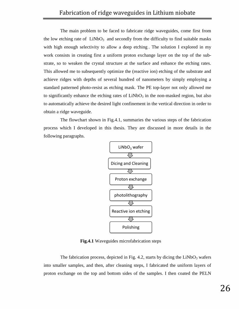
The flowchart shown in Fig.4.1, summaries the various steps of the fabrication
process which I developed in this thesis. They are discussed in more details in the
following paragraphs.
Fig.4.1 Waveguides microfabrication steps
The fabrication process, depicted in Fig. 4.2, starts by dicing the LiNbO3 wafers
into smaller samples, and then, after cleaning steps, I fabricated the uniform layers of
proton exchange on the top and bottom sides of the samples. I then coated the PELN
LiNbO3 wafer
Dicing and Cleaning
Proton exchange
photolithography
Reactive ion etching
Polishing
Page 36
Fabrication of ridge waveguides in Lithium niobate
27
samples with a uniform photoresist layer that I then patterned using photolithography
techniques in the nanofabrication clean room. I subsequently transferred the photoresist
pattern into the PELN substrates to the waveguides by means of reactive ion etching.
With higher (~m) ridges in LiNbO3, one could achieve an index increase as high as
Δn nLiNbO3 nAir~1.2 in the lateral (y) dimension, see Fig.4.2(c). If additionally proton-
exchange is used a refractive index step is also introduced in the vertical direction (z).
High-confinement of optical field can be then obtained over 2D cross section (y-z) as
shown in Fig.4.2(c).
At the end of the fabrication, I removed the photoresist mask and the edges of
the samples were polished in order to be able to couple light into the ridges and charac-
terize the guiding properties.
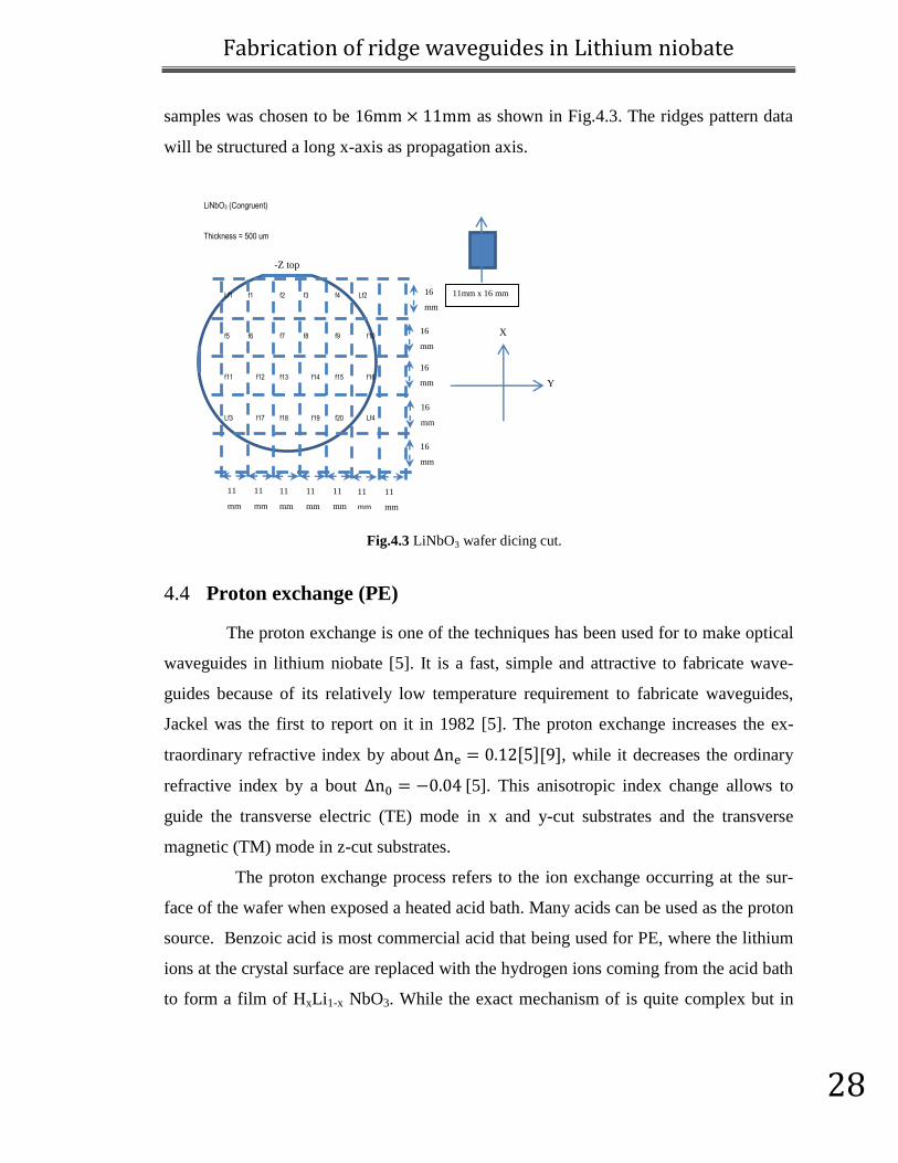
4.3 Preparations of samples
The starting materials were produced from commercial providers, in the form of
wafers of undoped and MgO-doped LiNbO3 with diameter 3 inches and thickness of
500 . A programmable dicing machine was used to cut the wafer. The size of the
Fig.4.2 Sample before (upper) and after (right) the etching process and after removing the photoresist
mask (lower).
LiNbO3
LiNbO3
LiNbO3
PELN
PELN
PELN
PR Mask
PR Mask
Plasma
Patterning of Photoresist
RIE
Waveguides
y
z
x
(a)
(b)
(c)
Page 37
Fabrication of ridge waveguides in Lithium niobate
28
samples was chosen to be 16 as shown in Fig.4.3. The ridges pattern data
will be structured a long x-axis as propagation axis.
4.4 Proton exchange (PE)
The proton exchange is one of the techniques has been used for to make optical
waveguides in lithium niobate [5]. It is a fast, simple and attractive to fabricate wave-
guides because of its relatively low temperature requirement to fabricate waveguides,
Jackel was the first to report on it in 1982 [5]. The proton exchange increases the ex-
traordinary refractive index by about , while it decreases the ordinary
refractive index by a bout [5]. This anisotropic index change allows to
guide the transverse electric (TE) mode in x and y-cut substrates and the transverse
magnetic (TM) mode in z-cut substrates.
The proton exchange process refers to the ion exchange occurring at the sur-
face of the wafer when exposed a heated acid bath. Many acids can be used as the proton
source. Benzoic acid is most commercial acid that being used for PE, where the lithium
ions at the crystal surface are replaced with the hydrogen ions coming from the acid bath
to form a film of HxLi1-x NbO3. While the exact mechanism of is quite complex but in
-Z top
11
mm
16
mm
11
mm
11
mm
11
mm
11
mm
11
mm
11
mm
16
mm
16
mm
16
mm
16
mm
f2
f3
f4
Lf2
f1
Lf1
f5
f6
Lf4
f20
f19
f18
f17
Lf3
f11
f12
f7
f8
f9
f10
f13
f14
f16
f15
X
Y
11mm x 16 mm
LiNbO3 (Congruent)
Thickness = 500 um
Fig.4.3 LiNbO3 wafer dicing cut.
Page 38
Fabrication of ridge waveguides in Lithium niobate
29
principle it could be described through chemical reaction, when the Benzoic acid used as
the proton source one could write the reaction as:
4.1
The acidity of the bath determines whether complete or partial exchange has taken place,
for the optical waveguides fabrication only partial exchange is necessary, by using
undiluted Benzoic acid, which is relatively weak acid.
system exhibits a complex chemistry structures, a number of phases
have been identify, the phase transition can be characterized by a discontinuity of the
index ( and / or of the deformation a long axis perpendicular to the surface plane,
they are indicated with , κ1, κ2, 1, 2, 3, 4 [10]. I used beta phase, which exhibit the
graded refractive index profile ~0.12, these phases can be plotting taking the stress
tensor of the crystal as a function of step index see Fig.4.4 below.
The thickness of the PE film dPE, is controllable by the process temperature and process
duration. The diffusion of the proton in the substrate that forming the depth of the PE
film layer can be described by the equation 4.2 as:
Fig.4.4 Deformation along crystal as a function of refractive step
index in Z cut substrate [10].
Page 39
Fabrication of ridge waveguides in Lithium niobate
30
Where tPE is duration of the process and is the constant of diffusion of the hydrogen
in LiNbO3 substrate surface, which is temperature-dependent. DPE is displays exponen-
tial energy activation function dependence, and can be written as:
where k is Boltzmann constant (k = 8.617343 ×10⁻⁵
eV K-1
), TPE is the temperature of
the process. Do and Ea depend on the crystal orientation [5] [11].
Fig.4.4 below shows the thicknesses of PELN layer for different temperature values
as a function of the process duration time.
Fig.4.5 PELN film thickness as function of temperature and process duration time.
By using equation 4.2 and Fig.4.5 above, PE process conditions were: TPE =
200, tPE=3.5 h for the temperature and duration process time respectively, it were used
to have a depth of PE layer ~ 1 µm, by taking the value of the diffusion coefficient as
Do = 1.8×109 µm
2/h and energy activation function Ea = 0.987 eV, from Bortz [12].
Fig.4.6 shows schematic for the setup that was used for the Proton exchange
process. The LiNbO3 samples were put in the acid heat bath, fixed to the upper side of
0 0.5 1 1.5 2 2.5 3 3.5 4 4.5 50
0.2
0.4
0.6
0.8
1
1.2
1.4
1.6
1.8
2
X: 3.5
Y: 0.9931
Time duration (tPE, hour)
Lay
er d
epth
(d
PE
, µ
m)
dPE vs tPE
T= 180 deg C
T= 190 deg C
T= 200 deg C
T= 210 deg C
T= 220 deg C
220 oC
210 oC
200 oC
180 oC
160 oC
Page 40
Fabrication of ridge waveguides in Lithium niobate
31
the setup box, while the lower one contains the benzoic acid, which was heated with
slowly gradient until 200oC. After the acid was melted the box was turned upside down
and the reaction took placed for 3.5 hours, according to the equation (4.1), to reach the
desired depth, then the process was stopped by turned it to the original side position, and
cooled slowly till reach back the room temperature. The depth that was achieved from
the process was measured using Metricon. See the fabrication results in 4.6.8 .
To remove the organic and inorganic contamination on the samples, that can
attached to the surface from PE process, handling, or surrounding environment, by doing
a normal cleaning process in an ultrasonic bath.
One way to determine the PE layer depth that achieved is to use the prism cou-
pler methods that describe in chapter 2. A Metricon, that use the same technique, was
used to measure the PELN layers depths.
References samples that have same PE condition process with other fabricated
sampled were used to measure the PE layer, C-LiNbO3 and MgO-LiNbO3.
The PE:LN layers depth were measured for both Z faces of the sample with the
Metricon and it was found to be about 1.4969 for C-LiNbO3, while it is 1.0721
of MgO-LiNbO3 samples.
Based on the experimental results, for the different depth I calculated the
experimental the diffusion coefficients for both undoped and MgO doped liNbO3 sam-
ples, using equation 4.1. This yielded that the diffusion coefficient for the proton
Fig.4.6 Proton exchange setup.
Page 41
Fabrication of ridge waveguides in Lithium niobate
32
exchange process at 200 oC is DPE = 0.16 µm
2/h and DPE = 0.071 µm
2/h for C-LiNbO3
and MgO-LiNbO3 respectively.
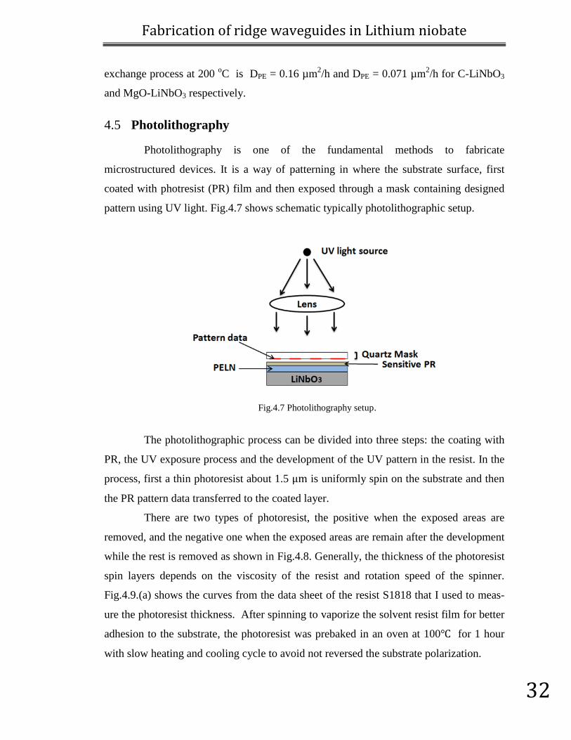
4.5 Photolithography
Photolithography is one of the fundamental methods to fabricate
microstructured devices. It is a way of patterning in where the substrate surface, first
coated with photresist (PR) film and then exposed through a mask containing designed
pattern using UV light. Fig.4.7 shows schematic typically photolithographic setup.
The photolithographic process can be divided into three steps: the coating with
PR, the UV exposure process and the development of the UV pattern in the resist. In the
process, first a thin photoresist about 1.5 is uniformly spin on the substrate and then
the PR pattern data transferred to the coated layer.
There are two types of photoresist, the positive when the exposed areas are
removed, and the negative one when the exposed areas are remain after the development
while the rest is removed as shown in Fig.4.8. Generally, the thickness of the photoresist
spin layers depends on the viscosity of the resist and rotation speed of the spinner.
Fig.4.9.(a) shows the curves from the data sheet of the resist S1818 that I used to meas-
ure the photoresist thickness. After spinning to vaporize the solvent resist film for better
adhesion to the substrate, the photoresist was prebaked in an oven at 100 for 1 hour
with slow heating and cooling cycle to avoid not reversed the substrate polarization.
Fig.4.7 Photolithography setup.
Page 42
Fabrication of ridge waveguides in Lithium niobate
33
The mask that I used for the resist exposure was made by chrome on quartz. A
Karl Suss MA4 mask aligner with a highly pressurized mercury lamp and a peak spec-
trum at a wavelength of 365 nm was used ultraviolet (UV) exposure. The ridge design
pattern of the mask used for the exposure had 12 set of ridges bands 10 mm long with
varying width from 1:1:12µm separated by 40 µm as shown in Fig.4.9 (b).
After exposure, the samples was dipped in the developer solution to remove the
exposed areas, the exposure and dipping times were determined by eye estimation to
have a good pattern, Fig 2.10 shows the resist pattern after the development process,
and Table 4.1 gives typically values and conditions used in the process.
Fig.4.10 The photoresist pattern after the development.
Fig.4.9 The thickness of the photoresist as a function of spin speed for Micropost
S1800 series [13] (a). The Mask used to write the lithography ridges pattern (b).
(b) (a)
Fig.4.8 The negative and positive types of photoresist.
Page 43
Fabrication of ridge waveguides in Lithium niobate
34
Table 4.1 the values that used to pattern the PR data
Photoresist type Positive type (S1818)
Spinning time 6000 r/min
Baking duration 1 hour (slowly gradient heating in oven)
Exposure time 3.5 s
Developer time 80 s
Post-baking duration 1 hour
After the process, the samples were rinsed in DI water, dried with compressed
air, and post baked to further increase the resistance against etching. Fig.4.11 shows the
widths parameters that were measured and Table 4.2 presents the results for the pattern
structures values that were obtained.
Table 4.2 PR pattern structure before the etching process in
Sample 1 2 3 4 5 6 7 8 9 10 11 12
C:LN
(-Z)
top -- 1.2 1.4 2.4 3.1 4.3 5.2 6.2 6.8 7.8 8.6 9.7
bottom -- 2.1 3.1 3.9 4.9 5.9 6.9 7.7 8.7 9.5 10.6 11.4
C:LN
(-Z)
top -- 1.1 1.7 2.4 3.2 4.2 5.1 6.0 6.7 7.9 8.7 9.6
bottom -- 1.7 2.9 3.7 4.7 5.8 6.9 7.6 8.4 9.5 10.4 11.4
MgO:LN
(+Z)
top -- 1.3 1.6 2.1 3.3 4.2 5.1 6.1 7.0 7.6 8.6 9.9
bottom -- 1.9 3.1 3.9 4.8 5.8 6.9 7.8 8.8 9.5 10.7 11.8
MgO:LN
(+Z)
top -- 1.6 1.7 2.3 3.2 4.3 5.0 6.0 7.0 7.7 8.9 10.0
bottom -- 2.1 2.8 4.0 5.0 5.9 6.6 8.0 8.7 9.5 10.6 11.4
Fig.4.11 The photoresist pattern
structure.
Page 44
Fabrication of ridge waveguides in Lithium niobate
35
4.6 The reactive ion etching
Many dry etching techniques are available which they use gaseous etchants,
such as Magnetically enhanced reactive etching (MERIE) [14] and Electron cyclotron
resonance (ECR) etching [15].
The reactive ion etching (RIE) is a simple easy controllable way to achieve a
good etching rate and to avoid isotropic processes in chemical wet etching. Good results
are expected by using the RIE and relatively large selectivity to enhance high structure
depth ridges and enhance anisotropy for vertical etching.
A schematic RIE chamber in the Fig.4.12 above is consist of a Vacuum chamber, RF
power as lower electrode plate (cathode) in same time it is work as sample holder, an
upper electrode (the grounded chamber) and the ICP generator.
The plasma system generates electron, ions, and free radicals (ions, atoms, mol-
ecules with unpaired electron, which may can have positive, negative or zero charge)
such as fluorine the one I used to attack the surface chemically. The Plasma is generated
by applied a strong Radio frequency, typically 13.56 MHz, the RF power supply is
attached to the electrode for to control the ion bombardment energy independently.
In appearance of low-pressure condition, and exist of fluorine (CHF3) and inert
(Ar) gas. The oscillating electric field ionized the gases molecules due to collisions
between the accelerated electrons and the etchants gases. During the process, any
electrons hit the chamber wall grounded, however the others stripped from the electrode
plate (wafer table) give a large positive charge about few hundred Volts, near the surface
region, this region called sheath reign or dark space. Then the relatively large voltage
Fig.4.12 Schematic RIE system.
Page 45
Fabrication of ridge waveguides in Lithium niobate
36
difference between the plasma and the RF electrode is tend to drift the negative ions
toward the wafer plate which cause the etching when reach the substrate surface.
The ions in the plasma can be accelerated by sheath field to high energies while
flowing to the substrate lead to energetic ion enhanced processes.
The ICP system is more effective at ions generation and a useful to have con-
trol to the ion density, for the little loss ions in the chamber wall, and it is possibility to
operate at low pressure which make the mean free bath of ions rather long.
4.6.1 The etching mechanisms
The Plasma etching mechanisms can be divided into four classes depending on
the type of interactions introduced:
1. The mechanical etching, which is due to ions bombardment.
2. The chemical etching, which occurs due to neutrals (atoms/molecules with no
charge) causing surface reactions.
3. The ion enhanced energetic etching.
4. The ion enhanced inhibitor etching.
Fig.4.10 and Fig.4.11 below show the main basic etching mechanisms adapted from [16]
In the first type see Fig.4.13 (a) above, the momentum transfer from accelerated
ions in the plasma removing material from the surface of the substrate and throws it
across the reactor chamber. This mechanism is called sputtering. The positive ions such
as (Ar+) ions are propelled into the surfaces by the negative going potentials at the edge
of the plasma. This mechanism requires low pressure and long free mean path, to let the
Fig.4.13 The etching basic mechanisms, mechanical (a), Chemical (b) adapted from [16].
Page 46
Fabrication of ridge waveguides in Lithium niobate
37
materials to leave the vicinity of the surface without being backscattered and re-
deposited. Sputtering is anisotropic process but has low selectivity.
In the second type of the mechanisms, the chemical one, see Fig.4.13 (b), the
active gas phase species, which usually are free radicals, and led to high chemical
reactions, e.g. fluorine atoms, in the plasma are, encounter the substrate surface, forming
volatile products. It effect is to etch and remove the surface substrate material in the
same way as the common chemical reactions occurring during wet etching, and usually
the process is therefore attack non-directional since the ion bombardment plays no role,
this produces isotropic circular etch profiles and etching undercut areas, except for some
preferential etch direction crystal. Its chemical reaction and the etches could guarantee
extremely high selectivity.
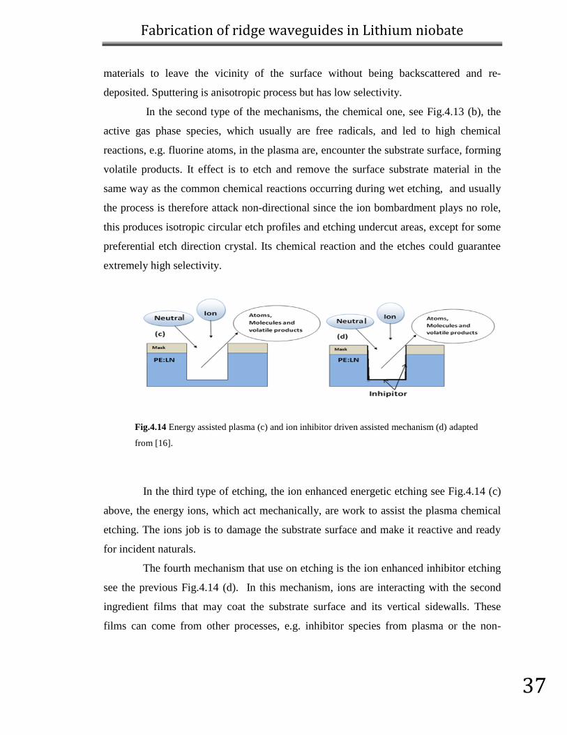
In the third type of etching, the ion enhanced energetic etching see Fig.4.14 (c)
above, the energy ions, which act mechanically, are work to assist the plasma chemical
etching. The ions job is to damage the substrate surface and make it reactive and ready
for incident naturals.
The fourth mechanism that use on etching is the ion enhanced inhibitor etching
see the previous Fig.4.14 (d). In this mechanism, ions are interacting with the second
ingredient films that may coat the substrate surface and its vertical sidewalls. These
films can come from other processes, e.g. inhibitor species from plasma or the non-
Fig.4.14 Energy assisted plasma (c) and ion inhibitor driven assisted mechanism (d) adapted
from [16].
Page 47
Fabrication of ridge waveguides in Lithium niobate
38
volatile process. The mechanism is work to solve the stop of the interaction with the
plasma and the substrate surface let to continuing the etching process.
4.6.2 Anisotropic plasma etching
Neutrals and the ions can work together in synergy to achieve high material re-
moval rates, exceeding the sum of the separate Sputtering and the chemical interaction
attacks. The neutrals directed and assisted by the ions bombardments, to cause the
anisotropic plasma etching.
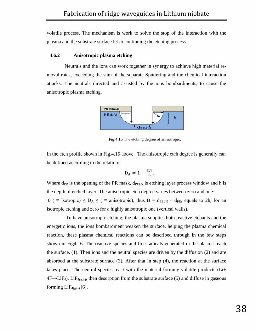
In the etch profile shown in Fig.4.15 above. The anisotropic etch degree is generally can
be defined according to the relation:
,
Where dPR is the opening of the PR mask, dPELN is etching layer process window and h is
the depth of etched layer. The anisotropic etch degree varies between zero and one:
0 ( ≡ Isotropic) ≤ DA ≤ ( ≡ anisotropic), thus B = dPELN − dPR, equals to 2h, for an
isotropic etching and zero for a highly anisotropic one (vertical walls).
To have anisotropic etching, the plasma supplies both reactive etchants and the
energetic ions, the ions bombardment weaken the surface, helping the plasma chemical
reaction, these plasma chemical reactions can be described through in the few steps
shown in Fig4.16. The reactive species and free radicals generated in the plasma reach
the surface. (1). Then ions and the neutral species are driven by the diffusion (2) and are
absorbed at the substrate surface (3). After that in step (4), the reaction at the surface
takes place. The neutral species react with the material forming volatile products (Li+
4F→LiF4), LiF4(ads), then desorption from the substrate surface (5) and diffuse in gaseous
forming LiF4(gas) [6].
Fig.4.15 The etching degree of anisotropic.
Page 48
Fabrication of ridge waveguides in Lithium niobate
39
4.6.3 The etching process in LiNbO3:
Plasma etching process is characterized by its selectivity, etch rate, uniformity,
and final surface quality. In my work, I explored the effect of several central parameters
to optimize the etching process, namely the reactor chamber pressure, radio frequency
RF input power, inductive coupled plasma (ICP) energy, gases flow rate and process
temperature.
Many recipes were studied, while working to enhance the etching rate. The
above parameters influence diametrical changes in the process results. See Table 4.3 it
shows some recipes I used looking for high selectivity working recipe with easy to
remove the photoresist after the etching, it shows the parameters affect, there are many
recipe with successfully easy to remove the PR. later in this chapter, I reported my work
around the final recipe that have peak in the selectivity, this study beside to investigate
the final recipe, also describes the influence with the parameters, the RIE process, it
shows how perfect same results, with same recipe using plasma etching can obtain.
Fig.4.16 Surface chemistry dry reaction etching steps.
Page 49
Fabrication of ridge waveguides in Lithium niobate
40
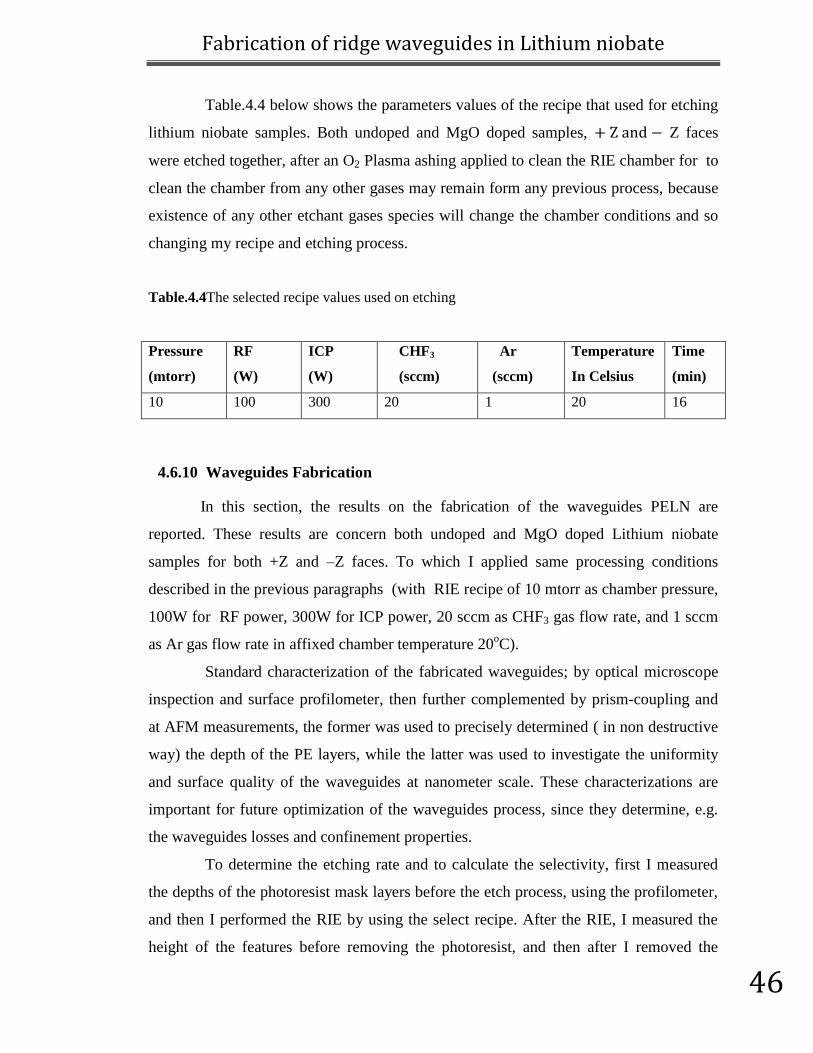
Table 4.3 Some selected recipes shows the parameters influences and their out come
Pressure
(mtorr)
CHF3
(sccm)
Ar
(sccm)
ICP
(W)
RF
(W)
Time
duration
(min)
Etching rate
(nm/min)
comments
LN PELN
20 20 2.5 200 50 10 2.39 12.80 Hard PR
20 30 2.5 200 50 10 ---- 5.24 Hard PR
10 20 2.5 200 60 10 6.29 32.59 Hard PR
10 70 2.5 200 100 10 5.06 39.26 Hard PR
20 90 2.5 200 100 10 ---- 20.70 Hard PR
40 70 2.5 200 100 10 ---- ----- Baked PR
20 90 2.5 300 100 10 ---- 46.00 Hard PR
4.6.4 The etch selectivity
The selectivity is the ratio between the etching rate of the layer to be processed
and the etching rate of the mask. A good selectivity ensures that the mask will not
remove during the process, which is important to achieve the required depth. In our case,
the process layer is PELN part and the mask is our photoresist part. Thus, the selectivity
is defined by the equation below
To maximize the selectivity the reactive species need to have the following proper-
ties:
1. Low etch-rate of the mask material over the layer being etched.
2. Low etch-rate of the materials under the layer being etched (etch stop layer).
3. High etch rate for the material being removed.
4. Excellent etching uniformity.
To calculate the selectivity we defined the etching rate as a measure of how fast the
material is removed in the etch process. This can be given by the equation below
Page 50
Fabrication of ridge waveguides in Lithium niobate
41
4.6.5 Pressure effect
The pressure influences the major phenomena that control the plasma etching.
When the pressure is low inside the etch chamber, there will be less reactants and a long
free path distance for the ions to move. Then by increase the potentials across the sheath
this can make the ions carry a higher energy momentum. These causes mainly sputter
etching. By increasing the pressure, one can on the other hand reduce the mean free
paths of the ions. The more frequent collisions between gaseous species lead to more
free radicals, thus at relatively high pressures the etch process will be mostly chemical.
However, the high ions energy is undesirable because of the decrease in selec-
tivity associated to the increase in the ions energy.
First I explored the pressure value on etching the LiNbO3 samples, many values
were tested, i.e. 10, 20 and 30 mtorr, while keep the other rest parameters fixed, as 70
sccm for CHF3, 2.5 sccm for Ar, 200W ICP and 200 oC for the chamber temperature,
for period of time 20 min each recipe. The recipe with the less pressure value gave a
profile depth 120 nm while the rest gave very low depth and unclear profile. Thus, I sat
my chamber to have low-pressure values, which agree with literature [16], and I used 10
mtorr for the final etching recipes, to have longest free path length for etchant species.
Moreover, I faced difficulties to ignite the plasma with pressure value low than selected
one.
4.6.6 Effect of Radio frequency and ICP powers
The Radio frequency RF power is applied to the cathode plate (the lower elec-
trode) to generate the plasma, and to influence the mechanical etching. An increase in
the RF power mainly cases increase on the energy of the bombardment ion.
I investigated many values for the RF power, with different etching recipes pa-
rameters with RF power values, e.g. 50W and 70W; I found etching rate was 5nm/min
and 20nm/min respectively.
A jump on the etching rate up to 30nm/min was achieved by increase the RF
value. The highest etching rate achieved at 100W, and when I increased the RF power
above 100W, e.g. 130W and 150W while the other parameters remain fixed, I observed
no significant etching rate, but instead the ion bombardment high energy heated the
Page 51
Fabrication of ridge waveguides in Lithium niobate
42
sample surface and baked the photoresist mask, making it hard to remove it. I used 100
W for the RF power value in my start point with 10 mtorr pressure, to optimize my
etching rate with ICP power and gaseous etchant parameters.
The Inductive Coupled Plasma ICP power increases the vertical magnetic field
through the plasma, which increases the number of electron-gas collisions number, and
therefore creates more ions. As a result, the ion density increased and more species that
are reactive will be sent to the substrate, which increases the chemical component of
etching. The advantage of using ICP RIE is that one could increase the ion density
numbers without increasing the energy. This is useful to avoid photresist baking, and
make it easy to remove.
As it shown in Fig.4.17, to investigate the peak using my ICP parameter, I per-
formed serial paths for the impact of ICP power and the etch rate of mask (red points)
and substrate (blue points).
By increasing, the ICP power starting from 100 W an increase in the etching
rate was registered, in both PELN layer and the Photoresist registered. This is while the
other recipe parameters are fixed specifically the pressure was 10 mtorr, the Ar gas flow
was 1.0 sccm, the CHF3 gas flow 20sccm and the RF power 100W. At a value of 300W,
I observed the highest etching rate, for the PELN layer. By increasing the ICP power
further, a decrease on the etching rate was registered for PELN layer, while the mask
Fig.4.17 Etching rate as a function of ICP power.
Page 52
Fabrication of ridge waveguides in Lithium niobate
43
etching rate increases, which means that above 300W the selectivity will decrease
(photoresist mask will be removed faster).
4.6.7 Etching rate and the etchants gases
One of the limits in the etching of LiNbO3 with Fluorine gases is due to the
redeposition of LiF, practically on the surface and sidewalls of the etch trenches see
Fig.4.14(d), which reduce etching rates and causes non-vertical etched walls [17]. A
solution to enhance the etching rate is to reduce the lithium concentration in the material.
Using the PELN process, as I discussed before in chapter 2 weaken the substrate surface
by exchange process reaction that I will describe it later here in this chapter, and there-
fore it likely also help to reduce the impact of LiF redeposition.
The fluorinate gas I used for my experiments was CHF3, and as I discussed
before, in order to achieve synergistic action (to get anisotropic deep etching) of the
mechanical and chemical I used a mixture of CHF3 and Ar gases.
For the chosen operating pressure 10 mtorr and RF power 100W, I studied the
effect of the CHF3 concentration of the etch rates of PELN and Photresist mask S1818.
Fig.4.18 shows the results obtained for a fixed Ar gas flow at fixed value 1.0
sccm at ICP 300W, RF 100W and pressure 10 mtorr, with different CHF3 concentration.
Fig.4.18 Etching rate as a function of CHF3 gas flow.
Page 53
Fabrication of ridge waveguides in Lithium niobate
44
CHF3 is used to produce in the plasma the chemically reactive species, which is
fluorine to etch and remove the target material PELN. By increasing the CHF3 gas flow
rate, a increasing on the PELN layer, see the blue dashes line, likely the photoresist mask
decreasing was registered. At a value of 20 sccm, I observed the highest etching rate, for
the PELN layer, this means the amount of the chemical reactive species work effective-
ly. By increasing the gas flow rate further, a decrease on the etching rate is registered for
PELN layer, while the mask etching rate keep decreasing, that because adding more
species decrease the mean free paths inside the reactor chamber, which lead to less
energy species react substrate surface.
For the chosen operating pressure 10 mtorr and RF power 100W, ICP power 300W, and
CHF3 20 sccm, I studied the effect of the Ar concentration of the etch rates of PELN
(blue line) and Photresist mask S1818(red line).
Fig.4.19 shows the results obtained with different Ar gas concentration. The
highest etching rate registered for both the PELN layer and the photoresist mask at the
Ar gas flow rate 1 sccm, and by increasing the gas flow rate lead to the increase reactive
species inside the chamber which give a reduce to mean free paths for the etchants.
Therefore, a decrease on etching rate was observed. Uses of the 1 sccm as working point
Fig.4.19 Ar gas affects on PELN and mask photo-resist.
Page 54
Fabrication of ridge waveguides in Lithium niobate
45
help to avoid the increases of the substrate thermal temperature, which cases baking of
the photoresist and make it hard to remove.
4.6.8 Temperature effect
The RIE process in generally lead to heating of the samples, because the accel-
erated ions bombardment hit the surface with high energy and due to the chemical
reaction between the reactive species and the substrate surface. During my studies, I
discovered that the temperature of the sample during the RIE has a profound influence
on etching. It is important in the process to distinguish between the gas temperature,
which is a complex function of local power input such as heat transfer and transport
phenomena, and the substrate surface temperatures. The surface temperature is play role
on the substrate etching, heating it lead to a baking layer surface, that may cause a
decrease on etching rate same as accurse hard photresist that difficult to remove with
normal cleaning solvent and process, e.g. acetone, removers, and plasma O2 cleaning.
I manage to enhance the etching rate and remove the hard photoresist see
Fig.4.20, using the acetone when cooling the substrate by controlling the backside of the
sample being etched. I used a tiny liquid layer on back of the substrate and simply fixed
it to the holder (quartz plate).
I studied many different temperatures values as working process temperature
(47oC, 37
oC, 29
oC, and 20
oC) the best working degree temperature for my recipe to etch
the PELN layer using a photoresist mask S1818 is 20oC.
4.6.9 Final recipe
By study the recipes results using the above parameters, and by investigate the
selected recipe, I used it and then report my study results as you will see later.
Fig.4.20 Hard Photoresist.
Page 55
Fabrication of ridge waveguides in Lithium niobate
46
Table.4.4 below shows the parameters values of the recipe that used for etching
lithium niobate samples. Both undoped and MgO doped samples, Z faces
were etched together, after an O2 Plasma ashing applied to clean the RIE chamber for to
clean the chamber from any other gases may remain form any previous process, because
existence of any other etchant gases species will change the chamber conditions and so
changing my recipe and etching process.
Table.4.4The selected recipe values used on etching
Pressure
(mtorr)
RF
(W)
ICP
(W)
CHF3
(sccm)
Ar
(sccm)
Temperature
In Celsius
Time
(min)
10 100 300 20 1 20 16
4.6.10 Waveguides Fabrication
In this section, the results on the fabrication of the waveguides PELN are
reported. These results are concern both undoped and MgO doped Lithium niobate
samples for both +Z and –Z faces. To which I applied same processing conditions
described in the previous paragraphs (with RIE recipe of 10 mtorr as chamber pressure,
100W for RF power, 300W for ICP power, 20 sccm as CHF3 gas flow rate, and 1 sccm
as Ar gas flow rate in affixed chamber temperature 20oC).
Standard characterization of the fabricated waveguides; by optical microscope
inspection and surface profilometer, then further complemented by prism-coupling and
at AFM measurements, the former was used to precisely determined ( in non destructive
way) the depth of the PE layers, while the latter was used to investigate the uniformity
and surface quality of the waveguides at nanometer scale. These characterizations are
important for future optimization of the waveguides process, since they determine, e.g.
the waveguides losses and confinement properties.
To determine the etching rate and to calculate the selectivity, first I measured
the depths of the photoresist mask layers before the etch process, using the profilometer,
and then I performed the RIE by using the select recipe. After the RIE, I measured the
height of the features before removing the photoresist, and then after I removed the
Page 56
Fabrication of ridge waveguides in Lithium niobate
47
photoresist mask I measured the depths of etched feature on the PELN. Table.4.5 shows
the original thickness of the photoresist (deposited at a rotation speed of about 6000
rpm), the thickness of the photoresist remaining after etching process, and the heights of
the ridges.
Table.4.5 Ridges measurements profiles
Sample
Process
face
Thickness
of PR
befor RIE
(nm)
Remain
PR
(nm)
PELN
etching
depth
(nm)
Etching
rate
PE
C:LN –Z 1550 130 500 31 nm/min
+Z 1485 210 480 30 nm/min
MgO:LN –Z 1570 310 305 19 nm/min
+Z 1415 365 290 18 nm/min
I can notice that, in an agreement with expectations, the etch rates with fluori-
nated RIE are slightly larger on the –Z face, compared to +Z one, for both undoped and
MgO doped LiNbO3. The diference between the etching rates was 9nm/min, these
different values according to the sample orientation and the positively charges electric
field, which form a barrier against the etch process.
On the other hand, from the summarized data it is also apparent that the etching
of MgO:LN is lower than that of the undoped material (by 30%).
Moreover, about 84 nm/min and 72 nm/min was the photoresist etching rate re-
spectively. The above results give a selectivity of 0.36 and 0.25 for both undoped and
MgO doped LiNbO3 respectively.
The etched patterns had sidewalls angles of 60 degrees for both undoped and
MgO doped proton exchange LiNbO3 was regardless of the depths and widths of the
etching, neither face ( nor the MgO doping. The average results for the sidewall
angle measurements are summarized in Table.4.6 .
Page 57
Fabrication of ridge waveguides in Lithium niobate
48
Table.4.6 Ridges sidewalls angles before the etching process.
Sample Process
face
Sidewall angle
( in degrees)
before etching
PE
C:LN
–Z 61
+Z 59
MgO:LN
–Z 63
+Z 60
The data above were obtained by measuring the top and the bottom of the feature widths
along photoresist pattern with the profilometer and then calculating the slopes and at last
taking the average value for each sample.
One way to investigate the surface roughness in nanoscale is to use an Atomic
Force Microscope (AFM) setup, Fig.4.21 shows a schematic typically to that used,
which the main part consist of sharp probe, laser diode, photo detector, and piezoelectric
scanning system, and a computer.
AFM is a technique which can provides a three dimension profile of the surface
on Nanometer scale, by measuring forces between a sharp probe (less than 10 nm), at
very short surface distance (0.2 10 nm probe sample separation). The probe is support-
ed on a flexible cantilever. Using tapping mode method, in which the probe “taps” on
the surface during the scanning, and contacting the surface at the bottom with a constant
oscillation amplitude swing, the tip gently touches the surface and records the small
Fig.4.21 Schematic setup typically used at AFM technique.
Page 58
Fabrication of ridge waveguides in Lithium niobate
49
force between the probe and the surface to images the substrate surface. Fig 4.22 show-
ing 3 output images scanned by an AFM for C-LiNbO3 –Z face.
This further investigation with AFM techniques, which is confirmed essentially
the above measurement on the angles and additionally allowed me to evaluate the
sidewalls roughness. The interplay of the high resolution in both lateral and orthogonal
directions and the non-destructive approach will give both high fidelity scans of the
surfaces and very accurate analyses of the roughness.
First by calculating the feature of the non- processed samples, the proton ex-
change ones. The table below summaries the roughness results of these samples:
Table.4.7 Roughness values for the non-processed samples
Sample +Z (nm) –Z (nm)
LN 2.15 3.75
MgO:LN 3.91 2.15
PE:LN 2.35 3.63
PE MgO:LN 3.84 2.68
For the virgin congruent LiNbO3 the roughness is very low (~few nm) and basi-
cally it is mainly due to topographic features of the final polishing of the wafers at the
end of the industrial growth and wafer cut process. A slight difference depending on the
polarization of the sample was measured, i.e. 1.5 nm deepest structures in the –Z face at
undoped sample and 1.5 nm deepest structures at +Z face in MgO doped sample, but no
appreciable variations due to PE were measured, i.e. for the undoped –Z face of 0.12 nm
Fig.4.22 AFM pictures of tapping mode scanning of C-LN waveguide (Height, amplitude
and phase signal respectively).
Page 59
Fabrication of ridge waveguides in Lithium niobate
50
and +Z face of 0.2 nm, while in MgO doped sample it was of 0.53 nm at –Z face and
0.07 in +Z one.
The other area that was scanned is the sidewalls area. This area is one of the
highest interests in my work; as a matter of fact the roughness of the sidewalls is a key
aspect for the optical properties of the waveguides in particular the guided mode losses.
The highest part of the ridges, i.e. the “Top” areas, which were protected by the
photoresist during the etching process, should be preserving the original roughness of the
PE samples. Also the reading with AFM registered for the areas between the ridges, i.e.
the “Bottom” areas, which were etched during the process, gives an indicator of rough-
ness damage produced by RIE on the substrate (
To analyse the roughness in the specific areas mentioned above, I used the
RMS values. For the means I used additional none preceded (±Z) LN samples as refer-
ence for the roughness. By scanning and analyzing the features of the etched samples
surfaces, and comparing them to the reference samples. Fig.4.23 is presented a 3D
sketch of the waveguide in order to identify the areas of interest; these pictures were
obtained by using the data we measured from the sample MgO- LiNbO3.
By scanning the top, bottom, and sidewalls for the proton exchange undoped
and MgO doped samples for both (±Z) faces. A summarize to the results obtained will
found in Table.4.8 .
Top
Bottom
Sidewalls
Fig.4.23 Top, bottom and Sidewalls MgO- LiNbO3.
Page 60
Fabrication of ridge waveguides in Lithium niobate
51
Table.4.8 The roughness summaries results of the ridge samples.
Sample Process face Top Bottom Sidewalls
PE
C:LN
–Z face 3.71 nm 1.36 nm 4.03 nm
+Z face 2.19 nm 1.57 nm 3.94 nm
MgO:LN
–Z face 2.95 nm 1.81 nm 5.40 nm
+Z face 3.57 nm 0.55 nm 4.73 nm
The roughness at the top of the ridges, Table.4.7 compares with the one of none
processed samples showed in the Table.4.6. This makes sense, since the top side of the
ridges were protected by the photoresist during the etching, there should not be any
appreciable variation of the roughness in comparison with none processed samples. This
also confirms the perfect removal of the photoresist mask with our standard (acetone)
cleaning process after the RIE.
The ridges waveguides fabricated in this C-LiNbO3 substrate samples are
roughly having a lateral sidewalls slope of ~ 60 º.
The bottom etched side also here is the smoothest one for both undoped and
MgO doped samples. The reactive ion etching process seems to reduce the roughness by
more than 40 % which is a positive outcome. The roughness of the sidewalls is higher
than in all the other areas and it seems not to be dependent on the polarization of the
substrates. In fact the sidewalls are the target of reactive species and chemical reactions
such as redoposition of LiF.
4.7 Ridges waveguides
The fabrication technique that is report in this master thesis achieved a 3D con-
figuration of ridges waveguides, the PELN layer was not completely etched, and still
Page 61
Fabrication of ridge waveguides in Lithium niobate
52
there is a layer on top of the LiNbO3 substrate. The ridges have sidewalls angles of about
60o this can be shown in schematic Fig.4.24 below.
For the undoped LiNbO3 sample the PELN layer depth of about 1.5 µm, by the
RIE technique a depth of about 500 nm and 480 nm for both –Z and +Z faces respec-
tively, and sidewall angle ~60o and surface roughness about 3.71nm and 2.19 nm on the
top (un etched areas), 1.36 nm and 1.57 nm at the bottom (the etched areas), and on the
sidewall about 4.03nm and 3.94 nm for both –Z and +Z faces respectively.
While for the MgO doped LiNbO3 sample the PELN layer depth of about 1.0
µm, by the RIE technique a depth of about 300nm of about 200nm less than the undoped
one, and same sidewall angle ~60o and a surfaces roughness about 2.95nm and 3.57 nm
on the top (un etched areas), 1.81nm and 0.55 nm at the bottom (the etched areas), and
on the sidewall about 5.40nm and 4.73 nm for both –Z and +Z faces respectively.
4.8 Summary of the fabrication
Lithium Niobate is a hard and relatively inert material, hence it is quite difficult
to etch. With the reactive ion etching (RIE) technique developed for this propose, I
obtained 500 300 nm depths in LiNbO3 substrates, with a simple photoresist mask by
using high-density plasma tools.
The fabrication that I followed consists of increasing first a uniform proton
exchange layer on the top of the substrates, so to weaken the crystal structure at the
surface and enhance the subsequent etching rates. This allowed an increase by 6 times in
the etching rate with respect to the ordinary material, and achieving ribs waveguides
Fig.4.24 Schematic C- LiNbO3 ridges waveguides.
Page 62
Fabrication of ridge waveguides in Lithium niobate
53
with depths of several hundred of nanometers by simply employing a standard patterned
photo-resist as etching mask. The PE top-layer not only allows to significantly enhanc-
ing the etching rates of LiNbO3 in the non-masked region, but also to automatically
achieve an index increase in the vertical direction, needed to confine light in both
directions, hence achieving ribs waveguides.
The reactive ion etching process has proved a strongly reduce the roughness of
the substrate (it passes from ~3 nm to ~1.4 nm all the samples). On the other hand the
roughness of the sidewalls which is important for the losses of the final waveguides
structures is higher than in the other areas.
The process yielded waveguides with approximately the same slope of the
sidewalls (~60º in all cases) for the different types of materials undoped and MgO doped
LiNbO3.
These fabrication and roughness preliminary results suggest there is no prefer-
ential side for fabricating ridges waveguides when choosing the C-LiNbO3, on the other
hand, the etching rate, side walls angles and of low roughness of the bottom and the
sides suggest that it is more convenient to fabricate ribs waveguides on the originally +Z
side when choosing MgO-LiNbO3.
Page 63
Fabrication of ridge waveguides in Lithium niobate
54
4.9 References
[1] H. Hu, A.P. Milenin, R.B. Wehrspohn, H. Hermann, W. Sohler, ”Plasma etching
of proton exchange lithium niobate”, J. Vac. Sci.tchnol. A. vol. 24, 1012 (2006).
[2] Z. Ren, P.J. Heard, J.M. Marshall, P.A. Thomas, and S.Yu, “Etching characteris-
tics of LiNbO3 in reactive ion etching and inductively coupled plasma”, J. Appl.
Phys. 103, 034109 (2008).
[3] R.V. Schmidt and I.P. Kaminow, “Metaldiffused optical waveguides in
LiNbO3”, Appl. Phys. Lett.25, 458 (1974).
[4] W. S. Yang,” Asymmetry ridge structure fabrication and reactive ion etching of
LiNbO3”, Optical materials, 27, 1642 (2005).
[5] J.L. Jackel, C.E. Rice, J.J. Veselka, “proton exchange for high index waveguides
in LiNbO3”, Appl. Phys. Lett, 41, 607 (1982).
[6] M. De Micheli, J. Botnieau, P. Sibillot and D.B. Ostrowsky, “Fabrication and
characterization of titanium indifused proton exchange waveguides in Lithium
niobate”, Opt.Comm, 42, 101(1982).
[7] M.N. Armenise,” fabrication techniques of the lithium niobate waveguides”,
IEE PRCEEDINGS,Vol.125, Pt. J, NO.2, APRIL(1988).
[8] R. S. Weis, T.K. Gaylord, “Lithium niobate: summary of physical properties
and crystal structure”, Applied Phys, 37, 191 (1985).
[9] K.K. Wong, GEC.J.Res, 3, 243 (1985).
[10] Yu. N.Korkishko and V.A. Fedorov, “Ion exchange in single crystal for integrat-
ed optics and optoelectronics”, Cambridge international science publishing,
England (1999).
[11] D.F. Clark, A.C.G Nutt, K.K. Wong, P.J.R. Laybourn, and R.M. De La Rue,
“Characterization of proton exchange slab optical waveguides in z cut”, J.
Appl.Phys.54, 6218 (1983).
[12] M.L. Bortz, “Quasi phase matched optical frequency conversion in lithium
niobate waveguides”, PhD. Dissertation, Department of Applied physics, Stan-
ford University, Stanford, USA (1994).
[13] Miroposit S1800 photoresist un-dyed series spin speed curves.
Page 64
Fabrication of ridge waveguides in Lithium niobate
55
[14] Winfried Sabisch, and Matthias Kratzer, Ralf Peter Brinkmann,” Energetic
neutral flux towards surfaces in a magnetically enhanced reactive ion etch-like
reactor”, J. Vac. Sci. Technol. A 21(4), 1205 (2003).
[15] Kouichi Ono, Mutumi Tuda, Hiroki Ootera, and Tatsuo Oomori, “Electron
cyclotron resonance plasma etching of Si with Cl2: plasma chemistry and
mechanisms”, pure & Appl. Chem, Vol.66, 1327 (1994).
[16] Daniel. L. Flamm, “Mechanism of the silicon etching in fluorine and
chlorinecontaining plasmas”, Pure and Appl. Chem., Vol.62, No.9, 1709 (1990).
[17] H. Hui, R. Ricken and W. Sohler, “Etching of Lithium niobate: form Ridge
waveguides to Photonic crystal structure”, Eindhoven, The Netherlands, June 11-
13-2008.
Page 65
Fabrication of ridge waveguides in Lithium niobate
56
5. Conclusion, further work and future developments
5.1 Summary
The aim of this Master thesis was the fabrication of ridge waveguides in nonlin-
ear crystals of the LiNbO3 family by microstructuring techniques. The ridge structures
used in this work would avoid the light spreading in the transverse dimension and keep
all the light well confined. A layer of PE was created as the core guiding and confine-
ment region on the Lithium niobate substrate.
Lithium niobate as reminded is an extensively studied material and there is still
a huge amount of interest around the material and its applications. For its manifold
properties, LiNbO3 is one of the most widely used crystals to realize many devices
employed in different field of science and technology. As matter of fact, LiNbO3 is
characterised by large pyroelectric, piezoelectric, nonlinear and electro-optic coefficients
and it is also employed for applications in which acoustic and acousto-optic properties
are necessary..
The MgO-doped Lithium Niobate combines the properties of the Congruent
Lithium Niobate by also assuring a wider field of application by reducing the photorefra-
tion. In this master thesis both Congruent and MgO-doped Lithium Niobate were used.
Photolithography patterning techniques were used to coat the substrate surface
with a resist film then patterned by exposure to UV light through a mask containing the
desired ridge pattern. Ridges with depths of several hundred of nanometres height were
then fabricated by reactive ion etching. A proper selectivity and a high resolution
structuring of LiNbO3 was achieved with a relatively simple photoresist mask, by
optimizing the reactive ion etching of the substrate.
5.2 Further work
The further work that can be done on the waveguides implies their optical
characterization concerning measurements of important parameters to determine the
waveguide performance such as effective indices, cutoff wavelengths for the different
propagation modes, insertion losses, modal intensity distributions and propagation loss,
the latter being a particular important parameter to evaluate for the case of ridge wave-
Page 66
Fabrication of ridge waveguides in Lithium niobate
57
guides (which can suffer from enhanced scattering losses due to roughness at the wall
surfaces).
5.3 Future developments
Further developments could involve the integration of such structures with
preexisting periodically poled ferroelectric gratings (PPLN) for high efficient frequency
conversion in the visible and near infrared spectral regions [1].
Because of the ferroelectric properties of the LiNbO3 crystal [2], by
applying a high voltage electrical pulse along its optical axis one can achieve a reversal
of the ferroelectric polarity through the crystal. Periodically Poled Lithium Niobate
(PPLN) structures fabricated by electric field poling are suitable for the quasi phase
matching of many nonlinear optical applications of practical interest, e.g. second har-
monic generation (SHG), difference frequency generation (DFG), and optical parametric
oscillation (OPO). In a broader perspective, domain engineered structures at micro and
nano scale lengths can open many interesting research topics [5]. By combining of
PPLN and waveguides structures, one can improve the conversion efficiencies compared
to bulk, due to the high energy density over a long interaction length Furthermore by
using MgO-LiNbO3 substrates one could suppress the photorefractive effect in applica-
tions where blue or green light is generated [3] [4].
Page 67
Fabrication of ridge waveguides in Lithium niobate
58
5.4 References
[1] Kiyohide Sakai, Yasuharu Koyata, and Yoshihito Hirano, “Blue light generation
in ridge waveguide MgO:LiNbO3 crystal pumped by a fiber Bragg grating stabi-
lizer laser diode”, Optics letters/ vol.32, No.16/ August 15 (2007).
[2] R. S. Weis, T.K. Gaylord, Applied Phys, “Lithium niobate: summary of physical
properties and crystal structure”, A 37, 191 (1985).
[3] D.H. Jundt, M.C.C Kajiyama, D.Djukic, M. Falk, “Optical methods to character-
ize crystal composition of MgO doped lithium neonate”, Journal of crystal growth,
312, 1109 (2010).
[4] M. Iwai, T. Yoshino, S. Yamaguchi, and M. Imaeda, “High power blue generation
from a periodically poled MgO-LiNbO3 ridge type waveguide by frequency
doubling of diode and pumped Nd:Y3L5O12 laser”, Applied physics letter, vol.83,
18 (2003).
[5] Sunao Kurimura, Yuji Kato, Masayuki Maruyama, Yusuke Usui, and Hirochika
Nakajima, “Quasi phase matched adhered ridge waveguide in LiNbO3”, Applied
physics letters, 89, 191123 (2006).