FABRICATION OF YBCO THIN FILMS BY PULSED LASER DEPOSITION TECHNIQUE AND THEIR CHARACTERIZATION A Thesis Submitted to the Graduate School of Engineering and Sciences of İzmir Institute of Technology in Partial Fulfillment of the Requirements for the Degree of MASTER OF SCIENCE in Physics by Şerife TOZAN December 2010 İZMİR
Transcript
i
FABRICATION OF YBCO THIN FILMS BY
PULSED LASER DEPOSITION TECHNIQUE AND THEIR CHARACTERIZATION
A Thesis Submitted to the Graduate School of Engineering and Sciences of
İzmir Institute of Technology in Partial Fulfillment of the Requirements for the Degree of
MASTER OF SCIENCE
in Physics
by
Şerife TOZAN
December 2010 İZMİR
ii
We approve the thesis of Şerife TOZAN
___________________________ Prof. Dr. Doğan ABUKAY Supervisor ___________________________ Prof. Dr. Bekir ÖZÇELİK Committee Member ___________________________ Doç. Dr. Mustafa TEPE Committee Member 24 December 2010 __________________________ _________________________ Prof. Dr. Nejat BULUT Prof. Dr. Durmuş Ali DEMİR Head of the Department of Physics Dean of the Graduate School of Engineering and Sciences
iii
ACKNOWLEDGEMENTS
I first would like to thank my advisor, Prof. Doğan Abukay, for his continuous
support during the master program and providing me with many opportunities and my
teacher, Prof. Durmuş Ali Demir, I never forget you.
I am also thankful to Assoc. Prof. Mustafa Tepe for his support as well as his
understanding in letting us use the laboratories at Ege University and Prof. Bekir
Özçelik for sharing all his experience with me. I want to thank to IYTE Material
Research Center staff for SEM, EDX, XRD, and AFM.
Thanks to each of my friends at Izmir Institute of Technology for providing a
great atmosphere and a wonderful work place. Especially, Canan Düztürk and Handan
Güneş have always been by my side and endured me. I also thank Fatma Yağız and İpek
Erdoğan, who are interested in my health problem.
Finally, I am indebted to my family SERKAN and SAADET TOZAN for their
support in all the choices I have made. I am forever grateful to my husband, TAYFUN
RÜZGAR, for his love and encouragement.
iv
ABSTRACT
FABRICATION OF YBCO THIN FILMS BY PULSED LASER DEPOSITION TECHNIQUE AND THEIR CHARACTERIZATION
This thesis focuses on pulsed laser deposition (PLD) system, fabrication of high
temperature superconducting YBCO thin films and their characterization. In this study,
the electrical and structural studies performed on laser deposited YBCO films have
shown that films produced by PLD. The thin films were characterized in detail by
employing structural XRD, SEM, EDX and AFM and electrical ( R-T) measurements.
During this work, pulsed laser deposition system used to grow superconducting
thin film on MgO single crystal substrate. Firstly PLD system was carried out by using
different growth parameters. Deposited films was cooled down in situ under an oxygen
atmosphere at a given pressure. The deposition tecnique has emerged as a very powerful
method to make composition and microstructure controlled superconducting YBCO
films.Thanks to rapid heating and evaporation of the target and interaction of the laser
beam with evaporated materials leading to formation of a high temperature plasma PLD
system is different from other thin film growth system.However, major problem was
particulates emmission which was shown SEM,we solved this problem by chaning
distance between target and substrate, and laser power. Furthermore Electron Dispersive
X-Ray Spectroscopy (EDX) method was used to identify the chemical contents of the
films.The relation between critical temperature and oxygen deficieny was investigated
by means of electrical resistance R(T) and x-ray diffraction measurements.Finally, our
results were compared to literature and explanied similarites.
v
ÖZET
YBCO İNCE FİLMLERİNİN PULS-LAZER YIĞMA TEKNİĞİYLE YAPILMASI ve KARAKTERİZASYONU
Bu çalışmanın temel amacı YBCO ince filmlerinin puls-lazer yığma (PLD)
tekniğiyle üretilmesi ve yapısal özelliklerinin incelenmesidir. Bu çalışmada lazer
yığmasıyla elde edilen filmlerin elektiksel yapısal özellikleri çalışılarak PLD sistemiyle
YBCO süperiletken filmler üretilmştir. İnce filmlerin yapısal XRD, SEM, EDX ve
AFM, elektriksel özellikleri de RT ve manyetik alınganlık ölçümleri kullanılarak detaylı
olarak karakterize edilmiştir.Bu çalışma sırasında MgO alt taşlar üzerine epitaxial
olarak büyütüldü.Öncelikle YBCO ince filmler, PLD sisteminde farklı büyütme
parametreleri kullanılarak yapıldı. Epitaxial olarak büyüyen filmler belirli bir basınçta
belli bir sıcaklıkta soğumaya bırakıldı.
PLD film büyütme tekniği kontrollu bir biçimde farklı bileşikte ve microyapıda
YBCO süperiletken ince film üretmek için güçlü bir methottur. PLD sistemi, hedef
malzeme yüksek sıcaklıkta lazer demetiyle gaz fazında buharlaştırılmasından dolayı
diğer film büyütme sistemlerinden farklıdır. Ancak SEM görüntülerinde görüldüğü gibi
çok fazla parçacık yayılması vardır. Lazerin gücünü ve hadefle malzeme arasındaki
mesayi değiştirerek bu sorunu çözdük. Ayrıca, Enerji Dağılımlı X-ışını Spektoskopisi
yöntemi filmin kimyasal içeriğini bulmak için kullanılmıştır.Kritik sıcaklıkla oksije
eksiklliği arasındki ilişli R(T) ve X-ışını kırınımı (XRD) ölçümleriyle incelenmiştir.
Sonuç olarak, bulduğumuz sonuçlar literaturle karşılaştırarak açıklandı.
vi
To my Lovely Family
vii
TABLE OF CONTENTS
LIST OF FIGURES ......................................................................................................... ix
LIST OF TABLES ........................................................................................................... xi
Table 3.3. Properties of substrate materials for microwave devices of high-Tc
Films ......................................................................................................... 21
Table 3.4. Physical properties of some oxide, metal and semiconductor
substrates for the growth of YBCO superconducting films ...................... 22
Table 3.5. Typical properties of single crystal MgO substrates ................................ 23
Table 5.1. Some deposition parameters of YBCO films grown on MgO .................. 59
1
CHAPTER 1
INTRODUCTION
Superconductivity was discovered in 1911 by Heike Kamerling Onnes, who was
studying the resistance of solid mercury .When he cooled it to the temperature of liquid
Helium, 4 degrees Kelvin, its resistance suddenly vanished. Onnes showed that many
metals like Pb, Hg, Sn and Al undergo a phase transition at some temperature Tc, to a
state having a zero resistance. The next step in understanding superconductivity is the
exclusion of magnetic flux in a superconductor, discovered by Meissner and
Oschsenfeld in 1933 (Onnes, 1911).
The properties of superconductors were unusual that it took decades to explore
many phenomena related with it. A satisfactory microscopic theory of superconductivity
was developed by Bardeen, L. Cooper and J. Schrieffer. They developed BCS theory to
explain the physical mechanism of superconductivity. This theory earned them the
Nobel Prize in 1972. According to the BCS theory, the attractive interaction between
electron and electon lead to directly by the interaction between the electrons and the
vibration crystal lattice in superconductor. This is known the electron-phonon
interaction. An electron in the lattice which moves through a conductor will attract
nearby positive charges. This deformation of the lattice is brought about another
electron with opposite spin to move into the region of higher positive charge density.
This increase in positive charge will attract another electron. The two electrons are held
together, called a Cooper Pair. Cooper pair which have opposite momentum and spin.
Nevertheless, in the superconducting state and in the absence of current flow a cooper
pair is a system with zero momentum and zero spin like a boson. Lattice imperfections
and vibration have no effect on cooper pairs. The total momentum the pair is zero so
that it moves without scattering in the lattice which leads to zero resistance (Barden,
1957).
In 1970s many elements and compounds were found to be superconducting
with higher superconducting transition temperatures. In 1986, Johannes George
Bednorz and Karl Alexander Müller discovered the first high temperature
superconducting materials out of metallic systems, namely ,
2
which consist of barium, lanthanum, copper and oxygen, which had a transition
temperature of 35 K (Nobel Prize in Physics, 1987) (Bednorz, 1986). It was shortly
found by M.K Wu that replacing the lanthanum with yttrium, making
(YBCO), raised the critical temperature to 92 K, which was economically important
because the cheap and easily available liquid nitrogen could be used as a refrigerant (at
atmospheric pressure, the boiling point of nitrogen 77 K) (Wu, 1987). Following the
discovery of the high Tc superconductivity, BSSCO (T 11OK (Maeda, 1988),
TBCCO (T 125K (Parkin, 1988) and Ba Ca Cu O T 130K
Figure 1.1. Discovery of materials with successively higher Tc ' s over the last century (it refers to a Nobel Prize for their discovers)
Since the discovery of he high Tc superconductor, many works have
concentrated on these new materials. One of the most important topics is the thin film
deposition because thin film growth is the basic technique for future electronic
application. However, epitaxial growth of high-Tc compounds in thin film form was
found to be challenging because the high-Tc materials have characteristic properties
which require growth conditions and growth techniques different from those used to
deposit films of classical superconductors like Nb or for films of semi-conductors like
3
Si or GaAs. Some of the difficulties associated with the fabrication of high-Tc thin films
the realization of correct elemental stoichiometry, proper oxygen content and optimum
crystallographic alignment in the films. A lot of progress have been made during the
current decades in solving the problems associated with the epitaxial growth of
high-Tc materials and now excellent films are being made, notably by laser
ablation, PLD.
The first report of a high-T, superconducting thin films about PLD, although
with reduced Tc was published by Somekh in 1987 within three months, Enomoto
(1987) were successful in obtaining films with high-Tc and critical current density (Ic).
Since then, thin films of HTSC have been reported by a large number of group
worldwide (Neifelt, 1988). Some techniques of growth require high temperature
annealing after growth (ex-situ) while some techniques grow a film in correct crystal
structure (in-situ). In preparing films by ex-situ annealing the metallic elements are
deposited in approximately the correct composition as an amorphous layer, usually in
compound form with oxygen and possibly fluorine. If they are deposited on suitable
substrates, subsequent annealing in air or oxygen at high temperature results in thin film
to crystallize by a solid state regrowth mechanism to form a polycrystalline layer
(Naito, 1987). Depending on the substrate, the films may be textured with one
orientation aligned in a particular direction or epitaxial with the same crystal orientation
as the underlying substrates. Since the crucial growth step takes place long after
deposition, the actual technique used to deposit the layer is of secondary importance. In
in-situ growth, the film is deposited in crystalline form and, although it may need some
low temperature annealing to achieve the correct oxygen stoichiometry, it requires no
substantial rearrangement of the lattice after growth. In-situ growth has several
advantages. For example, the lower temperature involved in in-situ growth minimizes
contamination from the substrate. In addition, single crystal films can be grown with
greatly improved physical properties and the film surface can be smooth. In this thesis,
we studied relevant work in the field of high temperature superconducting YBCO thin
films.This study include the pulsed laser deposition, fabrication of YBCO films and
their characterization The physical phenomena involved in then interaction of high
power nanosecond excimer-laser pulses with YBCO bulk targets resulting in ablation,
plasma formation and subsequent deposition of YBCO thin films have been studied.
This thesis is organized in three main parts. Theoretical background and PLD
system are discussed in Chapter 2 and Chapter 3. Experimantal methods involving
4
fabrication of YBCO thin films, PLD set up and measurement techniques explained
Chapter 4. The main result on grown YBCO films are presented in Chapter 5. The thesis
is summarized in Chapter 6.
5
CHAPTER 2
SUPERCONDUCTIVITY
2.1. Fundamental Properties of Superconductivity
Superconductivity means vanishing electrical resistance in a material below a
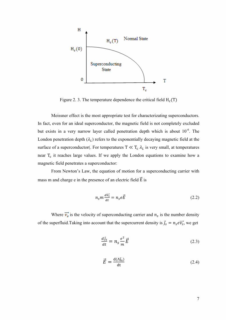
certain critical temperature Tc (Figure 2.1). Experimental works showed that above a
certain critical field Hc an applied magnetic field destroys the superconductivity. The
critical magnetic field is a function at temperature such that it tends to zero when the
temperature is close to Tc (Figure 2.4).
Figure 2.1. A temperature dependence of resistivity
The electrical current in superconductors flows without any resistance in the
material and therefore lasts forever. At temperatures below the transition temperature Tc
the magnetic flux is always expelled from superconductor regardless of the way in the
magnetic field is applied. In other words when we apply an external magnetic field
smaller than a certain critical field Hc, it is excluded by superconductor. This is called
meissner effect or perfect diamagnetism.
6
Figure 2.2. Diagram of the meissner effect (a) Magnetic field lines penetrate through a
superconductor at (b) Magnetic field lines are excluded from a superconductor when it is below its critical temperature (Source: Wikipedia, 2010)
Assume that the superconductor is cooled down below the critical temperature in
zero external magnetic fields. After that we apply an external field. The field does not
penetrate the interior of the sample as shown in Figure 2.2. Actually, immediately after
the field penetrates the surface layer of superconductor, an induced current is set up
which, according to Lenz’s Law, generates a magnetic field in the direction opposite to
that of the external field. Hence the total field in the interior of the specimen is zero.
Meissner and R. Ochsenfeld found that at T T the field inside a superconducting
specimen was always zero. However at T T , the resistivity of the specimen is finite
and, therefore, the magnetic field penetrates into it .It is shown schematically in Figure
2.2.b (Meissner, 1933).
0 1 (2.1)
7
Figure 2. 3. The temperature dependence the critical field H T
Meissner effect is the most appropriate test for characterizating superconductors.
In fact, even for an ideal superconductor, the magnetic field is not completely excluded
but exists in a very narrow layer called penetration depth which is about 10-6. The
London penetration depth ( ) refers to the exponentially decaying magnetic field at the
surface of a superconductor(. For temperatures T T is very small, at temperatures
near T it reaches large values. If we apply the London equations to examine how a
magnetic field penetrates a superconductor:
From Newton’s Law, the equation of motion for a superconducting carrier with
mass m and charge e in the presence of an electric field E is
(2.2)
Where is the velocity of superconducting carrier and is the number density
of the superfluid.Taking into account that the supercurrent density is , we get
(2.3)
(2.4)
8
(2.5)
Where is the London coefficient. (2.4) is known as the first London equation. Let us
take the curl of both sides of equation (2.4) and use
(2.6)
Maxwell equation (2.6). It gives
Λ B 0 (2.7)
Flux through an arbitrary area inside a sample with infinite conductivity stays
constant.
0 (2.8)
This is the second London equation. Taking the curl of the Maxwell equation
we obtain
(2.9)
With the vector identity . and using . 0 and the
second London equation;
Λ1λ
B
If we apply this equation to the superconductor with a magnetic field in the
region, 0 eq. (2.10) has the solution
(2.10)
9
(2.11)
This London equation can be used for obtaining the description of Meissner
effect in which the applied magnetic field decays exponentially inside the
superconductor with the characteristic decay length of London penetration depth , T
(temperature) dependence of empirical relation;
(2.12)
Figure 2.4. Schematic diyagram of the penetration of the magnetic field B inside the
superconductor according to london equation
Superconductors are divided into two groups,namely type І and type ІІ,
according to their response to a magnetic field. Type І superconductors are
characterized by expulsion of the magnetic field and by full diamagnetic behavior for all
field values below Hc, at which the solid reverts to the normal state (the meissner
effect). They have only a single critical magnetic field at which the solid undergoes a
first order phase transition. This behavior is found most pure metals such as Іn, Sn,
Hg…etc.
B
B0
2
10
Figure 2.5. The reversible magnetic behavior of Type superconductor
On the other hand, type ІІ superconductors have two critical fields; the lower
and the upper critical field which are H and H respectively. In type ІІ
superconductor the magnetic field does not penetrate the superconductor until it reaches
the lower critical field H H H . The average field in the interior of the specimen
is H 4πM is zero (meissner effect) that the type ІІ superconductor is still a
perfect diamagnetic. However, at H H H , steadily increasing field B
penetrates the superconductor and both the magnetic field and superconductivity
coexist. This state is known as the mixed state of the type ІІ superconductor. At a
certain field H H ,, the average field in the interior, B becomes equal to H and the
superconductivity is destroyed.
Figure 2.6. Type ІІ superconductors have two critical magnetic fields which are and ; below type ІІ behaves as type І, and above it becomes normal.
Above H , the type ІІ superconductor does not show the meissner effect.
Beyond , in the so called mixed state, the magnetic field penetrates the material in
11
vortices which arranged forming hexagonal lattice. The magnetic flux enters a type II
superconductor as fluxoids which consists of an integral number of a quantum known as
fluxon. Each fluxon containing a single flux quantum ( ) given by
2.07 10 (2.13)
The structure of a fluxon consists of a short-range (ξ) normal core surrounded by a long-
range vortex of supercurrent. As the field increased further beyond H , the density
of fluxons increases. Eventually, when the internal flux density equals to the applied
flux density at the upper critical field ( ), the cores of neighboring vortex overlap the
sample goes to normal state.
Figure 2.7. Schematic magnetic phase diagram of a type II superconductor
( Source: Poole, 1988)
If a current is flowing through the superconductor, in this mixed state, it
produces a Lorentz force acting on the vortices. The flux lines start to move under the
action of the Lorentz force at right angles to both the direction of the flux penetration
and the transport current which is given by
(2.14)
However, there are some sorts of defects or impurities in superconductors, such
as dislocation, walls, grain boundaries, voids, etc, in which the magnetic flux gets
12
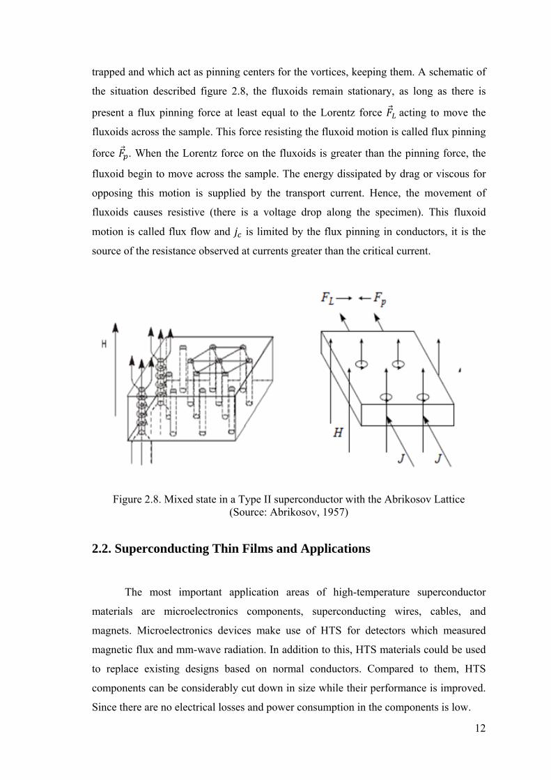
trapped and which act as pinning centers for the vortices, keeping them. A schematic of
the situation described figure 2.8, the fluxoids remain stationary, as long as there is
present a flux pinning force at least equal to the Lorentz force acting to move the
fluxoids across the sample. This force resisting the fluxoid motion is called flux pinning
force . When the Lorentz force on the fluxoids is greater than the pinning force, the
fluxoid begin to move across the sample. The energy dissipated by drag or viscous for
opposing this motion is supplied by the transport current. Hence, the movement of
fluxoids causes resistive (there is a voltage drop along the specimen). This fluxoid
motion is called flux flow and is limited by the flux pinning in conductors, it is the
source of the resistance observed at currents greater than the critical current.
Figure 2.8. Mixed state in a Type II superconductor with the Abrikosov Lattice
(Source: Abrikosov, 1957)
2.2. Superconducting Thin Films and Applications
The most important application areas of high-temperature superconductor
materials are microelectronics components, superconducting wires, cables, and
magnets. Microelectronics devices make use of HTS for detectors which measured
magnetic flux and mm-wave radiation. In addition to this, HTS materials could be used
to replace existing designs based on normal conductors. Compared to them, HTS
components can be considerably cut down in size while their performance is improved.
Since there are no electrical losses and power consumption in the components is low.
13
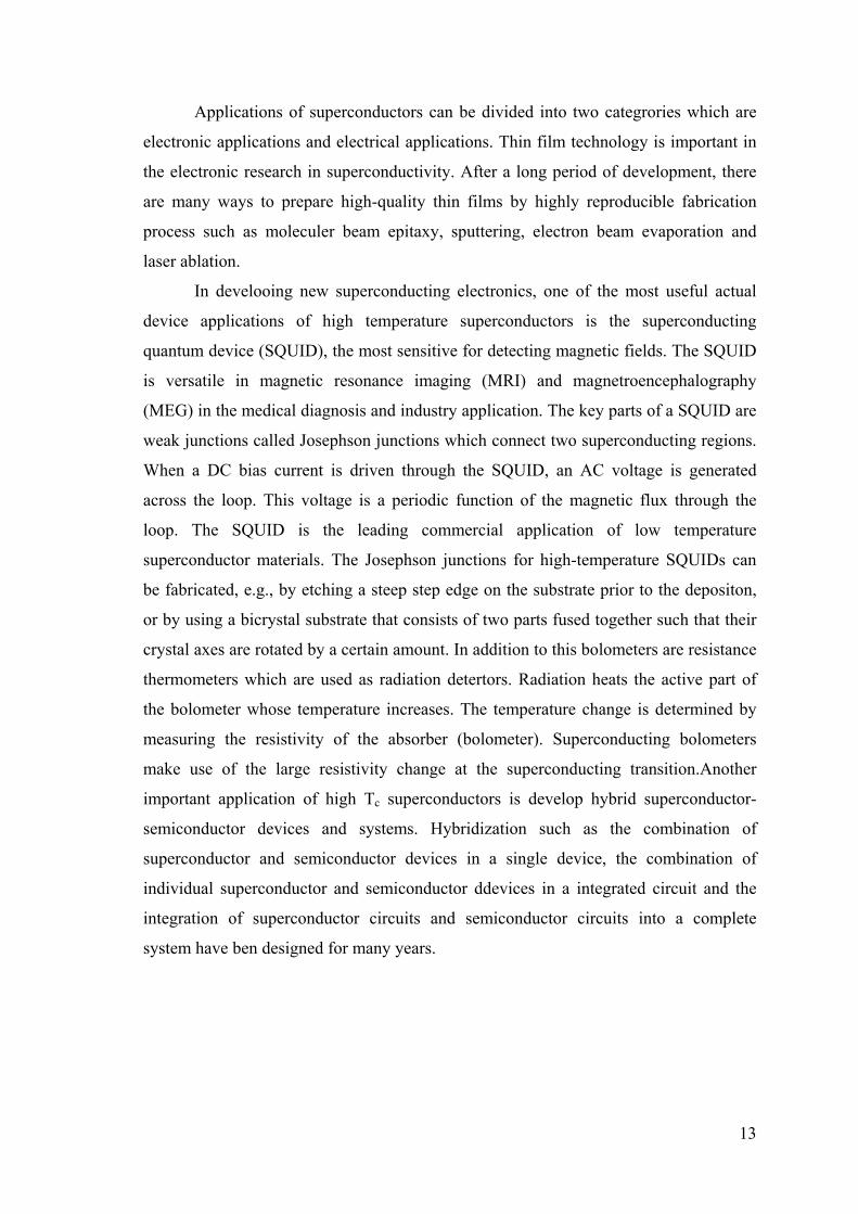
Applications of superconductors can be divided into two categrories which are
electronic applications and electrical applications. Thin film technology is important in
the electronic research in superconductivity. After a long period of development, there
are many ways to prepare high-quality thin films by highly reproducible fabrication
process such as moleculer beam epitaxy, sputtering, electron beam evaporation and
laser ablation.
In develooing new superconducting electronics, one of the most useful actual
device applications of high temperature superconductors is the superconducting
quantum device (SQUID), the most sensitive for detecting magnetic fields. The SQUID
is versatile in magnetic resonance imaging (MRI) and magnetroencephalography
(MEG) in the medical diagnosis and industry application. The key parts of a SQUID are
weak junctions called Josephson junctions which connect two superconducting regions.
When a DC bias current is driven through the SQUID, an AC voltage is generated
across the loop. This voltage is a periodic function of the magnetic flux through the
loop. The SQUID is the leading commercial application of low temperature
superconductor materials. The Josephson junctions for high-temperature SQUIDs can
be fabricated, e.g., by etching a steep step edge on the substrate prior to the depositon,
or by using a bicrystal substrate that consists of two parts fused together such that their
crystal axes are rotated by a certain amount. In addition to this bolometers are resistance
thermometers which are used as radiation detertors. Radiation heats the active part of
the bolometer whose temperature increases. The temperature change is determined by
measuring the resistivity of the absorber (bolometer). Superconducting bolometers
make use of the large resistivity change at the superconducting transition.Another
important application of high Tc superconductors is develop hybrid superconductor-
semiconductor devices and systems. Hybridization such as the combination of
superconductor and semiconductor devices in a single device, the combination of
individual superconductor and semiconductor ddevices in a integrated circuit and the
integration of superconductor circuits and semiconductor circuits into a complete
system have ben designed for many years.
14
CHAPTER 3
YBCO AND PLD
3.1. YBCO
3.1.1. Crystal Structure of YBCO
The crystallographic structure of high temperature superconductors has been
studied since their discovery for many research groups. Crystallographers classify the
structure of these oxides as of perovskite type with CuO2 planes lying normal to the
crystallographic c-direction. This is a common feature of these materials, hense they are
called cuprates. YBa Cu O δ (YBCO) is the most well known high temperature
superconductor, sometimes called the 1-2-3 compound. It was discovered in 1987 by
Wu .It is transition temperature is nearly 92K. It is well above the liquid nitrogen barier
(77K) and is relatively easy to synthesis. It is one of the members of the perovskite
ceramic family. The Y-Ba-Cu-O compound usually exhibits a stoichiometry ranging
from YBa2Cu3O6 (non- superconducting) to YBa2Cu3O7 (superconducting). Hence the
fabricated YBCO compound usually exhibits an oxygen deficiency, δ. The material is
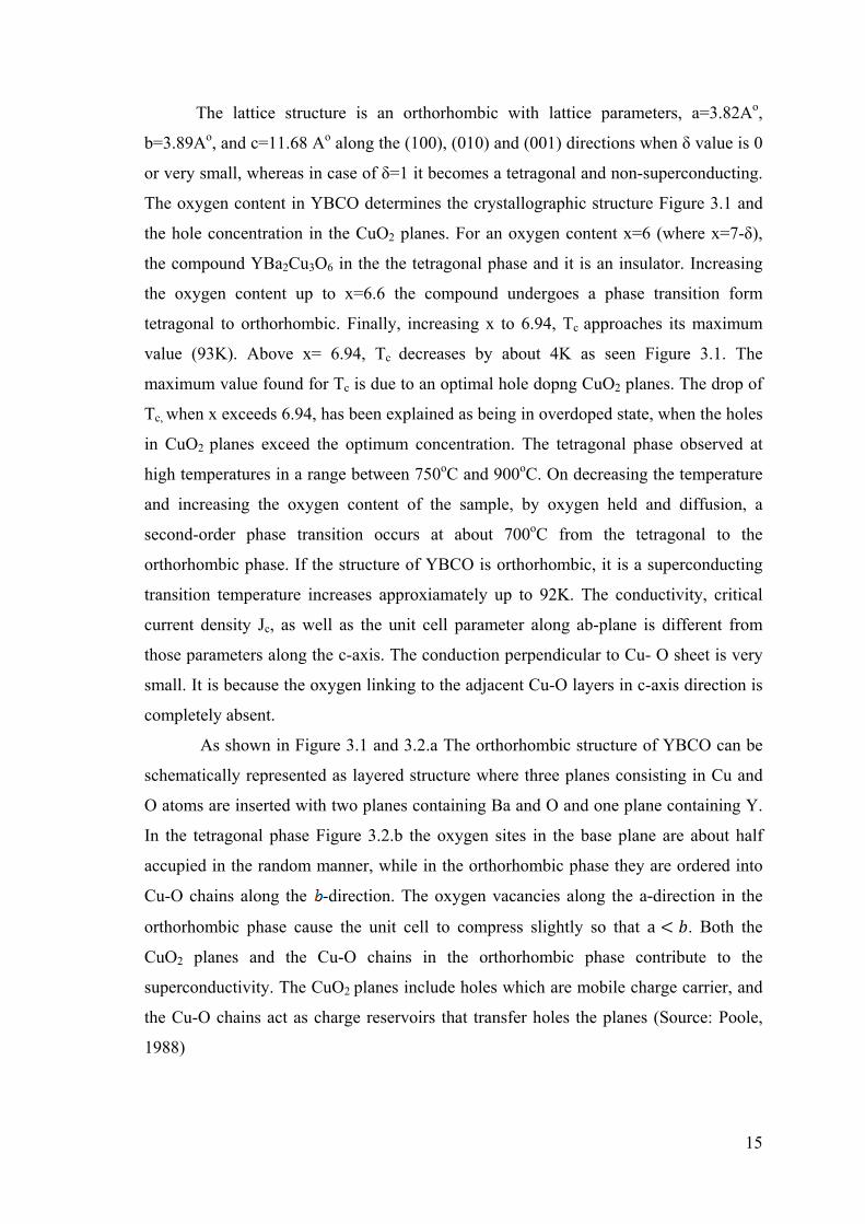
always referred to as YBa Cu O where 0 < δ < 1 (Jorgensen, 1990).
Figure 3.1. Phase diagram of YBa Cu O δ system as a function of oxygen content
and variation of Tc with oxygen content (Source: Poole, 1988)
15
The lattice structure is an orthorhombic with lattice parameters, a=3.82Ao,
b=3.89Ao, and c=11.68 Ao along the (100), (010) and (001) directions when δ value is 0
or very small, whereas in case of δ=1 it becomes a tetragonal and non-superconducting.
The oxygen content in YBCO determines the crystallographic structure Figure 3.1 and
the hole concentration in the CuO2 planes. For an oxygen content x=6 (where x=7-δ),
the compound YBa2Cu3O6 in the the tetragonal phase and it is an insulator. Increasing
the oxygen content up to x=6.6 the compound undergoes a phase transition form
tetragonal to orthorhombic. Finally, increasing x to 6.94, Tc approaches its maximum
value (93K). Above x= 6.94, Tc decreases by about 4K as seen Figure 3.1. The
maximum value found for Tc is due to an optimal hole dopng CuO2 planes. The drop of
Tc, when x exceeds 6.94, has been explained as being in overdoped state, when the holes
in CuO2 planes exceed the optimum concentration. The tetragonal phase observed at
high temperatures in a range between 750oC and 900oC. On decreasing the temperature
and increasing the oxygen content of the sample, by oxygen held and diffusion, a
second-order phase transition occurs at about 700oC from the tetragonal to the
orthorhombic phase. If the structure of YBCO is orthorhombic, it is a superconducting
transition temperature increases approxiamately up to 92K. The conductivity, critical
current density Jc, as well as the unit cell parameter along ab-plane is different from
those parameters along the c-axis. The conduction perpendicular to Cu- O sheet is very
small. It is because the oxygen linking to the adjacent Cu-O layers in c-axis direction is
completely absent.
As shown in Figure 3.1 and 3.2.a The orthorhombic structure of YBCO can be
schematically represented as layered structure where three planes consisting in Cu and
O atoms are inserted with two planes containing Ba and O and one plane containing Y.
In the tetragonal phase Figure 3.2.b the oxygen sites in the base plane are about half
accupied in the random manner, while in the orthorhombic phase they are ordered into
Cu-O chains along the -direction. The oxygen vacancies along the a-direction in the
orthorhombic phase cause the unit cell to compress slightly so that a . Both the
CuO2 planes and the Cu-O chains in the orthorhombic phase contribute to the
superconductivity. The CuO2 planes include holes which are mobile charge carrier, and
the Cu-O chains act as charge reservoirs that transfer holes the planes (Source: Poole,
1988)
16
Figure 3.2. Layering scheme of orthorhombic YBa2Cu3O7 (Source: Poole, 1988)
Figure 3.3. Sketches of the superconducting orthorhombic (a) and non superconducting tetragonal (Source: Jorgensan, 1987) (b) YBaCuO unit cells (Source: Schueller, 1987)
(a) (b)
17
3.1.2. Physical Parameters of
YBCO belongs to Type II of superconductors which are characterized by their
ability to maintain their superconducting properties in very high magnetic fields. These
superconductors accomplish this feat by a remarkable means. Instead of using the
energy required to completely expel the magnetic fields, the fileds are limited to an
internal aarray of normal-state flux tubes called vortices, for, they are surrounded by a
circulating supercurrent.YBCO epitaxial thin films manage to carry relatively large
current densities so they are used in device applications. The surface energy of an interface between YBCO and normal regions is negative
and hence the coherence length ( ) is less than the penetration depth ( ). The coherence
length might be thought of as a measure of the maximum distance between members of
a Cooper pair and determines the distance at which lattice interruptions can disrupt the
supercurrent. As a result, even twinnin planes or grain boundaries may have been
sufficiently large dimensions to act as weak links explains the relatively low values of Jc
seen in bulk seramic high-Tc superconductors. The penetration depth is a measure of the
depth of surface layer of superconductor up to which the magnetic field penetrates. The
values of coherence length, and some other physical parametersfor YBCO are given
in Table 3.1.
The layered structure of the copper oxide superconductors leads to strong
anisotropy in the normal and superconducting properties. The anisotrophy produces
dramatic changes in properties in the (Source: Roul 2006) a-b plane, parallel to the
layers, compared to the c direction, whih is perpendicular to the layers. The strong
uniaxial anisotrophy can be seen in the normal state resistivity and magnetic
susceptibility, and in the superconducting upper and lower critical fields. As listed in
Table 3.1 the anisotropy is caused by differences in values of and a long a-b plane
and along c-axis (Nahum, 1991).
18
Table 3.1. Physical Parameters of YBa Cu O δ (Source: Singh, 1989)
3.1.3. Thin Films of
Investigation on the electrical behavior of thin film materials have been
stimulated largely by the endustrial demand for microminiaturized electronic
components. The fundamental requirements for such a component are small size, high
thermal, low cost, mechanical and aging stability, small value of surface resistance, low
losses at a high-frequency and compatibility with the substrate used. These
requirements can be fulfilled to a large extend by thin films of suitable material. For
many significant applications of YBa Cu O thin films in electronic devices, suitable
substrates are necessary for achieving high-quality thin films.
19
3.1.4. Convenient Substrates for High-Tc Thin Films
The choice of substrates for high-Tc, thin films are very difficult as no ideal
substrate for high-Tc superconducting materials available to date. According to first
paper (Hollmann, 1996) which must be dealt with in determining the suitability of a
substrate for a high-Tc film is the chemical compatibility of the two materials. This
constraint is quite severe for high-Tc films, for, these materials are reactive with many
technologically important substrates, such as Si, GaAs and Al2O3 at the temperatures
required for the growth of high-Tc films. The substrate must also be compatible with
deposition processes and all subsequent processing for the use of the films. In addition
to this, regardless ofthe specific film growth method used, the substrate must be
unreactive in the oxygen-rich ambient required for growth and processing. The other
paper of concern in the selection of substrates for high Tc films is thermal expansion
match. A decent thermal expansion match between films and substrates is essential to
provide sufficient film adhesion and to avoid film cracking during thermal cycling.This
requirement is more relevant because of the fragility of these materials.
The best high-Tc films grown to date, as determined by a multitude of metrics,
including critical current density, morphology, and stability over time, are epitaxial on
their substrates. Epitaxial growth requires the controlled crystallographic orientation of
the film with respect to the substrate. In general, this requires matching of the film and
Atomically smooth surface Provide film uniformity and enable epitaxy
Perfect flatness
No porosity
Mechanical strength
Thermal coefficient of expansion equal
to that of deposited film
High thermal conductivity
Resistance to thermal shock
Thermal stability
Chemical stability
High electrical resistance
Low cost
Good lattice match
Provide mask definition
Prevent excessive outgassing and
improve film microstructure
Prevent film stress
Minimize film stress
Prevent heating of circuit components
Prevent damage and cracking during
processing
Permit heating during processing
Permit unlimited use of process
reagents
Provide insulation of circuit
components
Permit commercial application
Maximize crystalline perfection
Moreover, the dielectric properties of the substrate have significant effect on
high-frequency device performance. Appropriate dielectric properties and low value of
loss tangent are important factors in microwave and high-frequency device applications.
In order to successfully deposit film on substrate, the surface of the substrate must be
smooth and flat. Otherwise, any surface irregularities on substrates result in degraded
superconducting properties.
Substrates with low prices and large abound on the earth are beneficial for
scientific research, investment and production. Substrates most used for thin film
deposition are listed in table 3.3 and table 3.4 provides information that can be used to
select substrates for the growth of high-Tc thin film for microwave devices for YBCO
(Yamane, 1989)
21
Table 3.3. Properties of substrate materials for microwave devices of high-Tc Films (Source: Singh, 1989)
Material Tan Chemical stability
with respect to
YBCO
Twinning Mechanical
Strength
Available
Size(nm)
SrTiO3
LaGaO3
LaAlO3
NdGa03
YAlO3
PrGaO3
MgO
Al2O3
YSZ
CeO2
CaNdAlO4
SrLaAlO4
SrLaGaO4
LiNbO3
277
25
23
20
17
24
9.65
9.34
25
17
17
17
22-26
23-44
6x10⁻²(l00K,300GHz)
6x10⁻³(l00K,500GHz)
3 x10⁻⁵ (77 K,5GHz)
3 x10⁻⁴ (77 K,5GHz)
1x10⁻³(77K,10GHz)
3.6x10⁻⁴(300K,1kHz)
5x10⁻⁴ (100 K, 300
GHz)
3x10⁻⁵(77 K, 5 GHz)
8x10⁻³(l00K,300GHz)
1x10⁻³ (77 K,100
GHz)
5 x10⁻⁴(100 K, 8
GHz)
5 x10⁻⁵ (77 K, 5
GHz)
2x10⁻³( 300 K, 1
GHz)
Good
good
good
good
fair
good
good
poor
good
good
good
good
no
yes
yes
no
no
yes
no
no
no
no
no
good
fair
fair
fair
fair
poor
good
good
fair
fair
10x10
40
100
50
30
10
30x30
20x20
30
25
SrTiO3 is one of the most widely used substrates for growing high Tc
superconducting thin films. It posseses a perovskite structure and a good lattice match
with YBCO. Therefore, YBCO can be epitaxially grown on it. SrTiO3 also possesses a
smooth, flat surface with high chemical stability and small thermal expansion mismatch
with YBCO. But its large dielectric constant and poor high frequency properties make it
unacceptable for microwave device applications.Furthermore, this substrate is
considerably expensive. Therefore alternative substrates are necessary for mass
production of microwave electronic devices. The other substrate MgO has received a
good deal of interest in YBCO films deposition due to its modest dielectric constant,
good thermal expansion when matching with YBCO and, availability. In this study, we
used MgO substrates whose physical properties are given in detail in table 3.5.
22
Table 3.4. Physical properties of some oxide, metal and semiconductor substrates for the growth of YBCO superconducting films (Source: Singh, 1989)
Material
SrTiO3
LaGaO3
LaAIO3
NdGaO3
NdAIO3
YAlO3
PrGaO3
GdAIO3
EuAlO3
NdAIO3
PrAlO3
MgO
Al2O3
YSZ
CeO2
SrLaGaO4
Ag
Au
Cu
Pt
Si
Ge
GaAs
Crystal system
Cubic
Orthorhombic
Rhombohedral
Orthorhombic
Rhombohedral
Orthorhombic
Orthorhombic
Orthorhombic
Orthorhombic
Rhombohedral
Rhombohedral
Cubic
Trigonal
Cubic
Cubic
Tetragonal
Cubic
Cubic
Cubic
Cubic
Cubic
Cubic
Cubic
Lattice
Constant(AO) a b c
3.91
5.52 5.49
7.77
3.79
5.43 5.55
7.70
3.75
3.66 3.77
3.69
5.46 5.49
7.74
3.73 3.72
3.73
3.73 3.72
3.73
3.75
3.76
4.20
4.73
13.00
5.16
5.40
3.84
12.68
4.07
4.08
3.61
3.92
5.43
5.65
5.65
Melting Point
2353
2023
2453
1873
2363
2148
1680
1940
2060
2070
2080
3100
2300
3000
2900
1793
961
1064
1083
1772
1685
1231
1510
23
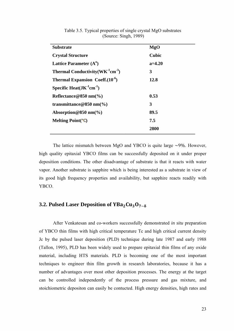
Table 3.5. Typical properties of single crystal MgO substrates (Source: Singh, 1989)
Substrate
Crystal Structure
Lattice Parameter (Ao)
Thermal Conductivity(WK-1cm-3)
Thermal Expansion Coeff.(10-6)
Specific Heat(JK-1cm-1)
Reflectance@850 nm(%)
transmittance@850 nm(%)
Absorption@850 nm(%)
Melting Point( )
MgO
Cubic
a=4.20
3
12.8
0.53
3
89.5
7.5
2800
The lattice mismatch between MgO and YBCO is quite large ~9%. However,
high quality epitaxial YBCO films can be successfully deposited on it under proper
deposition conditions. The other disadvantage of substrate is that it reacts with water
vapor. Another substrate is sapphire which is being interested as a substrate in view of
its good high frequency properties and availability, but sapphire reacts readily with
YBCO.
3.2. Pulsed Laser Deposition of
After Venkatesan and co-workers successfully demonstrated in situ preparation
of YBCO thin films with high critical temperature Tc and high critical current density
Jc by the pulsed laser deposition (PLD) technique during late 1987 and early 1988
(Tallon, 1995), PLD has been widely used to prepare epitaxial thin films of any oxide
material, including HTS materials. PLD is becoming one of the most important
techniques to engineer thin film growth in research laboratories, because it has a
number of advantages over most other deposition processes. The energy at the target
can be controlled independently of the process pressure and gas mixture, and
stoichiometric depositon can easily be contucted. High energy densities, high rates and
24
high process flexibility are characteristic features of the process. Furthermore, the
method is fast and cost effective way to produce high quality films (Venkatesan, 1996).
The essential process of PLD consists of melting and evaporating of target
materials with the pulsed laser beam. In PLD of YBCO thin films, a pulsed laser strikes
target which is a solid bulk YBCO. Some of the target materials are removed, escaping
in the form of a plume. Part of the plume comes in contact with surface of a heated
substrate kept away from the YBCO target.The plume, which consist building blocks of
the YBCO lattice, covers the substrate. The result is the fabrication of thin film of
YBCO materials with the same chemical structure as the target. PLD offers numerous
advantages, including film stoichiometry closed the target, high deposition rate, low
contamination level and non-equilibrium processing. Moreover, accessible experimental
parameter in PLD is very easy for the synthesis of high temperature superconducting
thin films. These parameters are the substrate temperature, the energy of the atom flux,
the relative and certain arrival rate of atoms for compound films and the pressure in the
chamber.
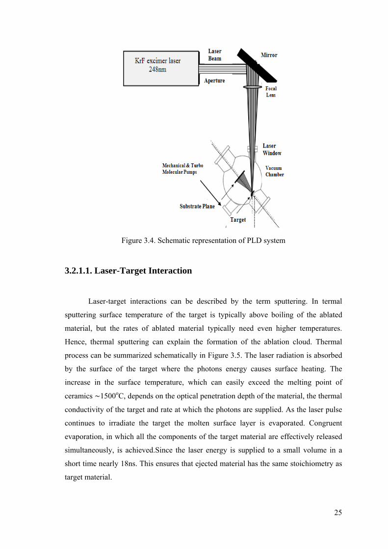
3.2.1. Pulsed Laser Deposition System
The basic experimental design for thin film deposition by laser ablation is
similar to other physical vapor deposition process. The apparatus includes a vacuum
chamber, a substrate holder with presice temperature control (heater) and target. Figure
3.4 is a schematic diagram of a typical PLD system. An excimer laser which operates
using a mixture of Kr, F2, He, and Ne generates pulses with a wavelength varying from
193nm to 308 nm is used for target ablation. The laser fluence is varied by either
varying the laser output energy or by focusing the beam.
The optical imaging system consists of a mirror and planoconcave lens. The
mirror has reflective coating surface. The laser beam is passed into the chamber by a
quartz window which is sensitive to damage if the laser energy density is too high or if
the window is covered by dust particles. Chamber has several quartz windows, one to
admit the laser beam while the others are for in-situ plasma diagnostics and monitoring
the growth. The growth chamber contains substrate holder with heater bock, a rotating
target holder and a shutter. The oxygen pressure during deposition is regulated using a
mass flow controller and a microvalve.
25
Figure 3.4. Schematic representation of PLD system
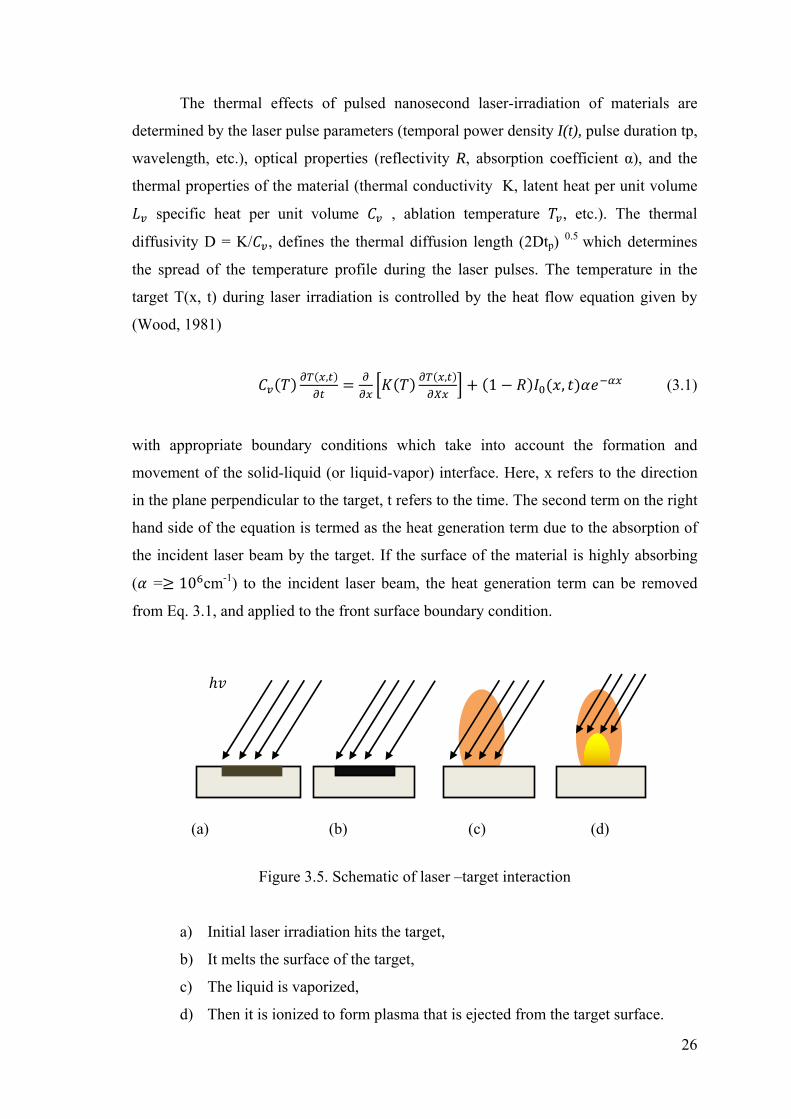
3.2.1.1. Laser-Target Interaction
Laser-target interactions can be described by the term sputtering. In termal
sputtering surface temperature of the target is typically above boiling of the ablated
material, but the rates of ablated material typically need even higher temperatures.
Hence, thermal sputtering can explain the formation of the ablation cloud. Thermal
process can be summarized schematically in Figure 3.5. The laser radiation is absorbed
by the surface of the target where the photons energy causes surface heating. The
increase in the surface temperature, which can easily exceed the melting point of
ceramics ~1500oC, depends on the optical penetration depth of the material, the thermal
conductivity of the target and rate at which the photons are supplied. As the laser pulse
continues to irradiate the target the molten surface layer is evaporated. Congruent
evaporation, in which all the components of the target material are effectively released
simultaneously, is achieved.Since the laser energy is supplied to a small volume in a
short time nearly 18ns. This ensures that ejected material has the same stoichiometry as
target material.
26
The thermal effects of pulsed nanosecond laser-irradiation of materials are
determined by the laser pulse parameters (temporal power density I(t), pulse duration tp,
wavelength, etc.), optical properties (reflectivity R, absorption coefficient α), and the
thermal properties of the material (thermal conductivity K, latent heat per unit volume
specific heat per unit volume , ablation temperature , etc.). The thermal
diffusivity D = K/ , defines the thermal diffusion length (2Dtp) 0.5 which determines
the spread of the temperature profile during the laser pulses. The temperature in the
target T(x, t) during laser irradiation is controlled by the heat flow equation given by
(Wood, 1981)
, , 1 , (3.1)
with appropriate boundary conditions which take into account the formation and
movement of the solid-liquid (or liquid-vapor) interface. Here, x refers to the direction
in the plane perpendicular to the target, t refers to the time. The second term on the right
hand side of the equation is termed as the heat generation term due to the absorption of
the incident laser beam by the target. If the surface of the material is highly absorbing
( = 10 cm-1) to the incident laser beam, the heat generation term can be removed
from Eq. 3.1, and applied to the front surface boundary condition.
Figure 3.5. Schematic of laser –target interaction
a) Initial laser irradiation hits the target,
b) It melts the surface of the target,
c) The liquid is vaporized,
d) Then it is ionized to form plasma that is ejected from the target surface.
(a) (b) (c) (d)
27
Briefly, laser-target interaction depends on the laser properties such as pulse
duration, intensity, wavelength and the target properties such as the vaporization
energy, absorption depth, specific heat, and thermal conductivity. Ablated materials due
to laser-target interactions produce plasma which includes high energetic species.
3.2.1.2. Plume-Laser Interaction
Heating of the target by the high intensity laser beam causes electronic
excitation of target atoms, ablation and exfoliation of the surface and plasma formation
(B r, 2004).This plasma absorbsfurther laser radiation by inelastic free electron
scattering (inverse Bremstrahlung) which causes it to be heated. As the plasma enlarges
the electron density decreases and the plasma becomes transparent to the laser radiation.
In this way the behavior of the plasma self-regulates the laser-target interaction. Plasma
can be determined as a quasi-neutral gas. It is formed when the content of particles such
as electrons, ions, neutral atoms, molecules, molten droplets and large particulates in the
vapor reach a critical value above the target. Because of the collision between these
particles, we see a luminous plasma plume. The flux of ions and electrons as a function
of temperature can be predicted by the Richardson’s and Langmuir-Saha equations,
respectively. Both of these equations show an exponential increase in the fraction of
ionized species with temperature. Higher ionized fractions than predicted by the
Langmuir-Saha equation have been observed in laser irradiated targets (Nakayama,
1984). This has been attributed to the higher temperatures induced by absorption of the
laser beam by the evaporating material and electron impact ionization.
The physical mechanisms involved in the absorption and reflection of the laser
energy by the evaporating material were identified in the early experiments as the
sources for very high temperature (~1 KeV) plasma. The penetration and absorption
of the laser beam by the plasma depends on the electron-ion density, temperature,
as well as the wavelength of the laser light. For penetration (or reflection) of the
incident laser beam the plasma frequency (vp) should be lower than the laser
frequency.
At a local thermal equilibrium, the degree of ionization of the plasma as a
function of density, temperature, and the ionization energies is determined by the Saha-
28
Eggert equation which can be derived from the Boltzman Distribution (Vankatesan,
1996):
(3.2)
where en , in , nn are the densities of electrons, ions and neutrons, Qe, Qi, Qn represent
the internal partition functions of electrons, ions, and neutrals, iψ is the ionization
potential of the neutral atom (Ho, 1996).
The degree of ionization depends on the laser parameters (such as wavelenght,
fluence and pulse duration) and properties of target material. The Saha-Eggert equation
is valid for weakly ionized plasmas for which the screening of the coulomb charge of
ions and electrons is negligible. This condition can be provided when Debye length is
sufficiently large.
Generally expansion of plasma is based on the evaporants from the target but
sometimes this situation can occur differently. Because of the formation of a plasma in
front of the target, the laser beam will be partially absorbed before it reaches the
target.It is called “plasma shielding”.Absorption of light in the plasma can be
determined by two mechanisms preeminently that are inverse bremsstrahlung and
photoionization of excited atoms (Chena, 2005) and the absorption coefficients for these
two mechanisms are:
2.90 10 / (3.3)
3.427 10 / (3.4)
where is absorption coefficient for electron-atom IB, is the absorption
coefficient for electron-ion IB, and are the electron and heavy-body temperatures,
and are the Gaunt factors for electron-atom IB and electron-ion IB, is the
frequency of the laser pulse (Liu, 1995).
3.427 10 / (3.4)
7.9 10 (3.5)
29
,where σ is the cross section in photoionization, Ei is the ionization energy of excited
state, hν is the photon energy of laser pulse, gI is the ambient gas ionization potential.
(Liu, 1995)
Heating by IB occurs to absorb radiation when the expansion of plasma
provokes an electron passing through the field of an ion. IB is the collisional absorbtion
of energy so it increases energy and the temperature of electron. If the intensity of laser
is necessarily high, the great plasma properties can be achieved by IB (Lunney, 1998).
Photoionization is the other mechanism for absorption in which an electromagnetic
radiation (photon) interacts with the target and ejects its electrons. Therefore it causes
the target materal separated into charged particles.
During the ablation process of metals, the photonic energy from the laser
radiation is combined with the target bulk. This situation brings about the ejection of
macroscopic particulates and therefore it can cause hazardous effects on film growth
(Willmott, 2000)
3.2.1.3. Plasma Expansion
Plasma expands freely and adiabatically in vacuum. It’s perpendicular to the
surface of the target. Because of the collisions between the particles in plasma, it’s
possible to see a weak light inside the chamber. During plama expansion, internal
thermal and ionization energies are converted into kinetic energies of the ablated
species (Mijatovic, 2004). For laser induced plasma, when there is a high pressure
thermodynamic gas in chamber, the adiabatic expansion develops because of
temperature dependency. During plasma expansion, temperature decreases. Also plume
density reduces and inversely proportional cube of the distance from the target. This
reduction causes a decrease in collision rate of particles in plume and is concluded with
direct motion towards the substrate due to random kinetic energy of particles.
It is very important to use background gas in PLD experiments because it
provides optimization of experimental parameters during the film production process
(Chena, 2005). Gases are generally used to thermalize the plasma species through
multiple collisions and to condensate significant materials from the target trough
ablation (Willmott, 2000). The expansion dynamics of the plasma highly depend on the
30
background gas pressure. Background gas can be a non-reactive or reactive gas. See
Figure 3. 6 (B r, 2004).
Figure 3.6. Stages of plasma expansion in backround gas environment: a) vertical
motion arising at the plume periphery broken line b) motion of the plume boundary point farthest from the plume axis z c) regions with the pressure increase in front part of the plume d) shock wave ahead of the plume
The expansion of the plasma in the background gas environment begins with the
movement of particles from the target and forming a particle cloud like a disk. The
cloud becomes enlarge because of plume velocity distribution (positon 1). When the
cloud pressure equals to background gas pressure, the plasma expands excessively
(position 2). After overexpansion its size becomes smaller and pressure of plasma
exceeds the pressure of the background gas (position 3). This situation results in the
expansion of plume again at which it has the same velocity as the background gas in the
shock front and finally expansion stops (position 4) (B r, 2004). Therefore background
gas in vacuum chamber slows down the plasma which results in the formation of shock
waves and causes its confinement which leads to stop motion. Expansion in background
gas atmosphere depends on the total energy of the plume and the ambient gas pressure.
To determine plasma expansion in the presence of background gas, the "drag
force " and the "blast wave " models are commonly seen in literature (Afonso, 1990). At
low pressures the drag-force model describes the expansion of plasma. In this model the
ejected species experiences a viscous force proportional to its velocity v through the
background gas.
For the high background gas pressures, expansion mechanism can be described
by blast-wave model. When plasma expands, it behaves as a piston so that it presses,
squezes, and accelerates the gas molecules. Due to this piston effect gas molecules
31
reach supersonic velocities with the formation of the shock waves (Gammino, 2003).
Shock wave formation is caused by the sudden release of energy and is observed in
blast-wave model for high background gas pressures. In this model the propagation of
shock waves are described through the background gas.
In PLD experiments both of these mechanisms are combined to explain
expansion of plasma. At the beginning of the expansion it begins with the drag-force
model at low temperatures then plasma starts to slow in order to form shock front
through a background gas so it expands according to blast-wave model.
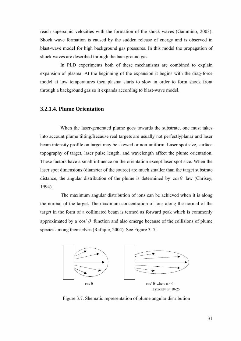
3.2.1.4. Plume Orientation
When the laser-generated plume goes towards the substrate, one must takes
into account plume tilting.Because real targets are usually not perfectlyplanar and laser
beam intensity profile on target may be skewed or non-uniform. Laser spot size, surface
topography of target, laser pulse length, and wavelength affect the plume orientation.
These factors have a small influence on the orientation except laser spot size. When the
laser spot dimensions (diameter of the source) are much smaller than the target substrate
distance, the angular distribution of the plume is determined by cosθ law (Chrisey,
1994).
The maximum angular distribution of ions can be achieved when it is along
the normal of the target. The maximum concentration of ions along the normal of the
target in the form of a collimated beam is termed as forward peak which is commonly
approximated by a cosn θ function and also emerge because of the collisions of plume
species among themselves (Rafique, 2004). See Figure 3. 7:
Figure 3.7. Shematic representation of plume angular distribution
32
Therefore the total orientation can be expressed as in below and generally this
equation can be applied to all particles in plasma (Ohring, 1997):
(3.6)
In the background gas environment is the angular distribution of plume extents.
It is an advantage since narrow angular distribution of plume can cause contamination
in chamber with respect to high deposition rate.
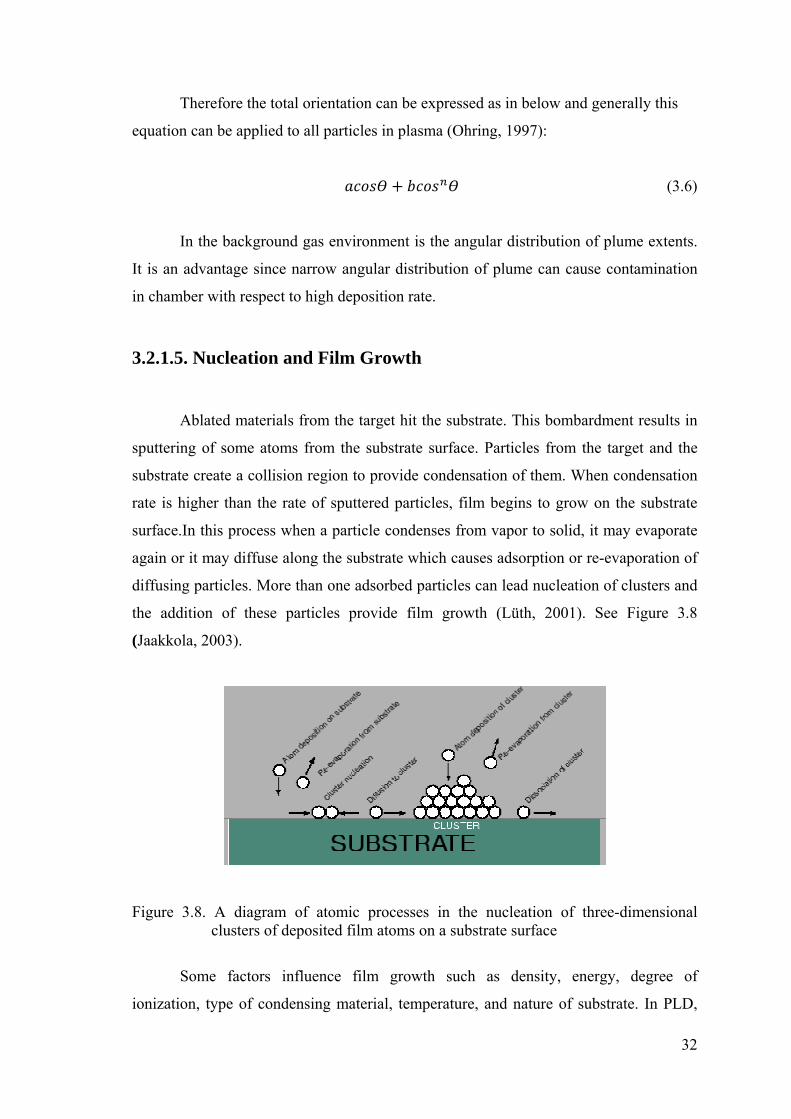
3.2.1.5. Nucleation and Film Growth
Ablated materials from the target hit the substrate. This bombardment results in
sputtering of some atoms from the substrate surface. Particles from the target and the
substrate create a collision region to provide condensation of them. When condensation
rate is higher than the rate of sputtered particles, film begins to grow on the substrate
surface.In this process when a particle condenses from vapor to solid, it may evaporate
again or it may diffuse along the substrate which causes adsorption or re-evaporation of
diffusing particles. More than one adsorbed particles can lead nucleation of clusters and
the addition of these particles provide film growth (Lüth, 2001). See Figure 3.8
(Jaakkola, 2003).
Figure 3.8. A diagram of atomic processes in the nucleation of three-dimensional clusters of deposited film atoms on a substrate surface
Some factors influence film growth such as density, energy, degree of
ionization, type of condensing material, temperature, and nature of substrate. In PLD,
33
the growing film is usually not in thermodynamic equilibrium and kinetic effects have
to be taken into account, which lead to the occurance of different growth modes
(Satischandra, 2005). There are three types of thin film growth mode which are called
island growth (Volmer-Weber, 3dimensional cluster), layer by layer growth (Frank-van
der Merwe, 2dimensional cluster), and layer + island growth (Stranski-Krastanov). In
layer-by-layer growth, nucleation of each next layer occurs only after the previous layer
is completed. There is a stong bonding between the substrate and layer atoms in this
mode.
This stage in PLD is very important because surface morphology of film
depends on the nucletion and growth mechanism. Nucleation causes condensation of
species from gas to solid phase and provides the creation of surface steps and
subsequent growth causes lateral movement of these steps. When supersaturated gas
phase is reached, the nuclei begin to form. The formation of nuclei depends on the
activation energy. After a critical density is reached, the nuclei grow and crystallization
begins to develop (Satischandra, 2005).
When a particle transfers from the gas phase to the condensed phase of the
deposited film, it is determined by a Gibbs free enthalpy:
∆ ∆μ (3.7)
At equilibrium, particle must obey;
μ μ , (3.8)
where P0 (t) equals to equilibrium vapor pressure. But, if the particle changes from
vapor to solid at a pressure P, the free entalphy changes:
∆ ∆μ where = (3.9)
Where is called the degree of supersaturation.
Nucleation and growth mechanism depends predominantly on the
supersaturation. Layer-by-layer growth is favored with increasing supersaturation.
Small supersaturation causes large nuclei. In this condition islands are created then
34
grow and caolesce on the substrate surface. On the other hand when the supersaturation
increases, the critical nucleus begins to shrink and lastly its shape transforms into a two
dimensional layer from its first shape that is like a cap.Also another important
parameter is substrate temperature. Many nuclei from under high evaporation rates
generally have low probability to grow on the substrate if the substrate temperature is
low and it causes fine-grained film. On the other hand atoms can be frozen and so they
stick on the substrate due to low substrate temperature. This condition does not allow
the surface diffusion and it can cause amorphous or disordered film. When the
temperature is high, if there are a few nuclei, a coarse-grained film occur (Ohring,
1995).
It is possible to see growth diagram for films from R-T dependence of N99. It is
the mean thickness at which a growing, thin and discontinuous film is given by the
equation (Metev, 1989).
N 0.5 exp (3.10)
where is the adatom (vapor atom) vibrational frequency, is the density of
absorption sites on substrate, E is the activation energy for adatom desorption, E is
the activation energy of adatom surface diffusion. By observing growth diagram, low
and high islands growth regions can be seen.
3.2.1.6. Macroscopic Particulate Production
The ejection of macroscopic particulate are called “laser droplets” which are
caused by photomechanical effects and forces due to laser-induced stress between bulk
metal and plasma. Also hydrodynamic sputtering intends forming of droplets at the
target due to transient melting and after melting there are some roughness that occurs at
the target surface. These laser droplets on the film surface can severely deteriorate the
film quality and morphology. Laser droplets provoke 3 challences: subsurface boiling,
recoil ejection and exfoliation (Willmott, 2000) In order to prevent splashing, a velocity selector as a particle filter can be
replaced between the target and the substrate to remove slow particles. Experimental
results are the evidence of the utility of the velocity filtration (Pechen, 1995). YBCO
35
films are studied by electron microscopy is shown in figure. In Figure 3.9.a the surface
of the film is covered with laser droplets without using particle filter. In Figure 3.9.b,
laser droplets disappear owing to particle filter.
Figure 3. 9. Surfaces of YBCO films prepared on MgO substrates without (a) and with (b) velocity filtration of the laser-induced streams
The other avoidance method is to use smooth and dense targets or liquid target
(Krebs, 2003) Also, positon of target or laser can be changed to achieve the best
geometry for avoiding splashing and laser droplets. The convenient geometry can be
achieved by putting substrate parallel with respect to the axis of the expanding plasma
cloud. Therefore, heavier droplets pass when atomic and ionic species are deposited
because of the collisions with molecules of the background gas. Another method is
reduction of laser energy density (Doughty, 1995). By using these methods films can be
growth without laser droplets.
3.2.1.7. Atomic Oxygen and Processing Geometry in the Growth of
Films
Since atomic and ionic species ar more reactive compared to their molecular
counterparts, it seems to be quite possible to obtain good quality YBCO films at lower
in situ growth temperature by supplying a flux of atomic oxygen to the lattice of YBCO
right during its formation. This concept has,in fact, been used by some PLD research
groups to grow good quality YBCO films at relatively low deposition temperatures
(Zheng, 1989) Singh have reported that an oxygen jet placed near YBCO target during
PLD produces a strong atomic beam which results in the formation of YBCO films at
lower temperatures than used for the growth of YBCO films in absence of such atomic
36
beam. According to Singh, the location of oxygen nozzle (i.e., whether it should be
near the target or near the substrate or in the middle of target-substrate, please see
Figure 3.11) also plays very crucial role in oxygen-incorporation to the film. The effect
of oxygen-jet geometries on the superconducting quality of YBCO films have been
presented in Figure 3.11 which shows the YBCO films obtained by positioning the
oxygen-jet towards the substrate has higher T, than that of YBCO films obtained by
positioning the oxygen-jet towards the target. The oxygen nozzle located near the target
may generate more atomic or ionic oxygen, but such geometry is likely to interfere
unfavorably by thermalizing the ablated species (Singh, 1989). The positioning of
oxygen nozzle near the substrate assists the incorporation of oxygen during the film
growth. A minute observation of the experimental set-up in these studies reveals that the
oxygen jet was pointing in the same direction (i.e., towards the substrates) even though
they were located at different position. Thus, what appears to be important and
unambiguous is the generation of atomic oxygen which enables one to grow YBCO
films with good quality at lower temperatures.
Figure 3.10. Schematic diagram of the laser deposition method showing the layout of
the oxygen-jet directed differently
Target
Substrate Heater Substrate
Power Supply
Oxygen Nozzle
Laser PowerLaser
37
Figure 3.11. Normalized resistance vs. temperature plots for (a) YBCO film obtained
while oxygen-jet was pointing towards the substrate (b) YBCO films obtained while oxygen-jet was pointing towards the target during laser deposition (Source: Singh, 1989)
38
CHAPTER 4
EXPERIMENTAL
4.1. YBCO Target Preaparation
In this study, we prepared a YBCO target.The sample was a mixture of Y2O3,
BaCO3 and CuO which were mixed in ratio of Y: Ba: Cu = 1:2:3.
0.5(Y2O3) + 2(BaCO3) + 3(CuO) YBa Cu O + 2CO2 (4.1)
This mixture was intimately mixed by grinding either in an agate ball mill or by
grinding in agate mortar. The grinding times were of the order of 30 minutes to one
hour until it was the uniformity of particle size. Tube furnace was used. The grinded
material was as first step to calcine as loose in Al2O3 crucible at 920º C in air. This took
24 hours. After cooling to room temperature the black product was regrinded.when a
big pellet pressed under pressure of 80 pa was made having diameter 25mm and
thickness 3mm, this pellet was put for last sintering at 930º C for 48 hours with several
intermittent regrindings. The cooling after the last sintering step and the subsequent heat
treatment were always performed in an oxygen atmosphere. The YBa Cu O sample
resistance at room temperature was 11 35Ω. Polycristalline superconductor
YBa Cu O was characterized by various methods, such as Meissner effect x-ray
diffraction and EDX.
39
Figure 4.1. Target Preparation
4.2. YBCO Thin Film Deposition System; PLD
A new PLD system was set up with up a multi-target capability with a Neocera 6
multi-target carrousel. The light source used for these deposition experiments was a KrF
excimer laser with dielectric rare mirror for 248 nm and uncoated MgF2 window for all
wavelengths. The laser has a wavelength of 248 nm, which is very effective for
congruent ablation within 25 nm range. Tested pulse energy is 145 mJ, but we use that
during deposition pulse energy is between 70 mJ and 100 mJ for low energy density.
The energy density is varied by either laser output or beam size on the target. Laser
beam dimensions are 11x7mm2 and can be adjusted by means of demagnification.The
laser beam was focused by two perpendicularly assembled cylindrical lenses, situated
outside the chamber. The focused laser beam was 45o from the target normal, and the
plume was generally perpendicular to the target surface. The energy loss from laser to
lenses is 25%. The loss of the residual energy at the lens and the window is nearly 10%.
40
The total energy loss approximately is 37.5%. Pulsed duration is 18 ns of FWHM (full
width at half maximum) and a pulse repetition rate is 5 Hz for our parameters.
Vacuum chamber provides base pressure nearly 10-6 torr with a turbo molecular
pump. The maximum pressure drop is 10-8 with it. The oxygen pressure of the chamber
is controlled by valve controllers (fine, coarse, target), a flow metering valve. The
multi-target capability up to six targets allows producing many different compositions
in a single deposition run to arrive at optimum composition having the desired material
properties. There are two shields between the target and the substrate. One is a fixed
shield which is protecting the other targets on the carousel from contaminations during
the ablation of the active target. The other shield is working as a shutter and it is located
in front of the substrate. Its function is to protect substrate by blocking the plume when
target cleaning (preablation) or target changing during deposition. The conductive
heater is attached in the vacuum chamber, which has maximum temperature 950oC with
temperature controller. Heater and substrate holder are placed in front of target.In
addition, target change and rotation can be controlled automatically by program
provided by Neocera.
Figure 4.2. Control Window for Neocera PLD automation package
Writen programe as below:
Firstly we opened Neocera PLD page. After target raster angle, velocity,
substrate holder velocity, shutter angle were entered from routine editor.
41
These parameters are;
• Target
Desired angle: 0
Start angle: 15o
End angle: -15o
Velocity: 47o/s
Rotate: 11o/s
• Substrate
Home offset: 180o
Velocity: 25o/s
• Pulse
Number of pulse: 900 shot ; preablation, 15000 shot; deposition.
Repetition Rate : 5hz
• Shutter Position
Closed: 48o
Open: 20o
For loading: 100o
Velocity:10 o/s
After entered these parameters, we wrote two routine programm which are
preablation 900s 5Hz YBCO-X on MgO/SrTiO3 raster from 15 to -15 sub.vel 25 shutter
closed and deposition 15000s 5Hz YBCO-X on MgO/SrTiO3 raster from 15 to -15
sub.vel 25 shutter opened. As soon as we finished routine program, we opened loop
editor to load program which was written.
Add line
Edit line
Load file
Select preablation 900s 5Hz YBCO-X on MgO/SrTiO3 raster from 15 to -15 sub.vel 25
shutter closed
Update Change
Add line after
Edit line
Load file
Select deposition 15000s 5Hz YBCO-X on MgO/SrTiO3 raster from 15 to -15 sub.vel 25
shutter opened
42
Update Change, Save
Write programme name.
Return the main Neocera PLD page and load program
Start Program.
Figure 4.3. The schematics of the PLD set up used for this work
4.3. YBCO Thin Film Deposition
The substrates used in this work were mainly MgO (100) and single-side
polished to average roughness Ra<1nm. The selection of MgO substrate was because of
their modest dielectric constant, good thermal expansion. The substrate size was
5x5x0.5mm and cleaned with various chemicals. Respectively it was cleaned with
acetone and alcohol in an ultrasonic cleaner nearly 45 minutes. After drying with
pressurized nitrogen the substrate was laid on top of a small drop silver paste placed at
off axis of the substrate plate and we waited that the silver paste spread easily to the
edges of the substrate thanks to its weight. Before put the chamber, possible dust
particles was removed from substrate using pressurized nitrogen. MgO has received a
good deal of interest in YBCO films deposition due to its modest dielectric constant,
43
good thermal expansion when matching with YBCO and, availability. The lattice
mismatch between MgO and YBCO is quite large ~ 9%. However, high-quality
epitaxial YBCO films can be successfully deposited on it under proper deposition
conditions. The other drawback of MgO substrate is that it eacts with water vapor.
Hence, we conserved it from air contamination and water. The distance between target
and substrate was 75 mm. The deposition chamber was filled with nitrogen and the plate
was slid into the tracks of the substrate heater. At this point, one should check the
condition of the target such as raster angle and its velocity. Pld system was pumped by
two different vacuum pumps which are a rough pump and a turbo molecular pump. The
Rough pump that is a mechanical pump, can pump down from atmospheric to 10-4 torr
and the turbomolecular pump reduces the pressure 10-8 torr. Before the deposition, the
vacuum is usually better than 5x10⁻⁶ torr. The Oxygen was used as background gas.
After putting substrate and target, we waited that the base pressure was 3x10⁻⁶ torr.
When the heater reached approximately at 800oC, we waited 30 minutes, for the
substrate temperature is homogeneous. The two step growth which are preablation and deposition were done. The first
step is preablation to remove contamination of target surface that is cleaning target
(number of pulses 900 shot and repetition rate 5 Hz). It taked 50 minutes (the number of
pulses 15000 and repetition rate 5 Hz). The background gas pressure 300mtorr during
the preablation and the deposition are controlled both upstream and downstream, with a
pin valve on the Oxygen delivery and with the adjustment of the gate valve on the
pumping port, respectively. In this way, a robust control of pressure inside the
deposition chamber can be achieved within a wide range. In preablation step, the shutter
closed and laser energy density is 1.83J/cm2. After this process, the shutter was opened
and at the same pressure deposition was started. The deposition recipe for YBCO on the
MgO substrates thin films is showed Figure 4.5 the deposition started by turning on the
laser at the selected pulse-repetition rate (5Hz). The laser-spot position on the target was
directed towards off axis position on the deposition plate. The colour, the shape of
plume and the colour depend above all on the oxygen pressure. The deposition time was
50 minutes and according to deposition time its thickness according to deposition time
is approximately 0,08nm/s. After the deposition process, the laser was switch off and
post annealing begins. This step is necessarily to allow the formation of the
superconducting lattice configuration. The TMP pump was switched off and the oxygen
pressure is slowly increased to nearly 400-500 torr. The temperature of the deposition
44
plate decreased from 800oC to 550oC by 10oC/min. The system was hold in this state for
an hour to ensure sufficient oxidation of the film. After annealing, the heater decreased
to room temperature. The heater and the targets had to be cooled down for several
hours. The chamber was filled with nitrogen. The substrate was removed from the
plate.The film was stored in a small plastic box and it was put in desicator to prevent
contamination of air.
Figure 4.4. Deposition recipes for YBCO films on MgO
Figure 4.5. Distance between target and substrate.
75mm
45
Figure 4.6. Plume ejected from YBCO during deposition process
4.4. Characterization and Measurements
During this work, film quality immediately was tested by measuring resistance
at the room temperature after the film was grown and removed from vacuum. The
resistance changed from 250Ω to 700Ω. Transition temperature was measured by R-T
measurement in the cryostat. To designate transition temperature of the prepared YBCO
thin films, four-probe method was used. Fabricated films are characterized by x-ray
diffraction (XRD), scanning electron microscopy (SEM), atomic force microscopy
(AFM) and energy-dispersive X-ray spectroscopy (EDX) in an effort to analyze crystal
structure, surface morphology and elemental composition to decide the deposition
parameters.
4.4. 1. Scanning Electron Microscopy (SEM) and Electron Dispersive
X-Ray (EDX) Analysis
The scanning electron microscopy (SEM) technique, which is a type of electron
microscopy, was used to determine the microstructure of the films to know information
46
about surface morphologies of the grown films on MgO substrates. This technique is
very usefull for a quick assessment of the entire surface area of a given film, whereas
other, perhaps more sensitive methods (AFM) are somewhat slower and allow
examination of only limited area of the sample. Using characterization our films by
SEM, we had deposition parameters changed such as repetition rate, deposition time.
Distance between target and substrate. In addition to this after film deposition and
prepare YBCO target, Electron Dispersive X-Ray (EDX) was used to learn the chemical
contents of them. Y, Ba, Cu, O contents were detect By EDX. According to collected
EDX data we decided how long the film exposure oxygen.
SEM works with electrons instead of light. These electrons are liberated by a
field emission source under high voltage. The incident electrons cause low-energy
secondary electrons to be generated and some escaped from the surface. The secondary
electrons emitted from the sample, the angle and velocity of these secondary electrons
relating to the surface structure of the object are detected. A detector catches the
secondary electrons and produces an electronic signal. This signal is amplified and
transformed into a video scan-image that can be seen on a monitor or to a digital image.
4.4.2. X-Ray Diffraction (XRD) Analysis
X-ray diffraction (XRD) has been proved to be a valuable technique for the
structure characterization of materials. The X-Ray Diffraction method was used in our
study to define the crystal structure of the YBCO films. 2 diffraction scan, which can
give information on the phase, orientation and lattice parameters of the thin film under
test.These films grown on MgO substrates and YBCO target were scanned in from
2θ 5°C to 80° . Using XRD results, we had deposition parameters changed whether
the oxygen was enough at grown YBCO films on MgO or not.
4.4.3. R-T Measurements
The critical temperature, where the superconductor loses all resistance to the
flow of electrical current, indicated that the material might be a superconductor. To
measure R-T we used (He closed cycle) croyostat decreased in 4K. Determine the
47
critical temperature of the sample a four-point method was used for R-T by Teknis
Firm.
Dc resistance was characterized by four-point probe technique to measure R vs
T. Four electrode probes were placed on the surface of the thin film. The cryostat
chamber was evacuated to 5x10⁻⁵ torr and the temperature was cooled down from 300K
to 4K by a helium gas compressor. A constant current source was attached to the outher
contacts with silver paints with a 10µA agitatin current, while the voltage drop between
the inner contacts were measured via a nanovoltmeter. It was measured by KEITHLY
2400. After putting film in the cryostat, it was pumped by vacuum pump. We waited
that the vacuum decreased in below 5x10⁻⁵ torr. As soon as the pressure was in the
range of 10-5 torr, the cooling was started. It took about 3 hours to bring the sample to
the minimum temperature, 4K. Firstly we set point at 290 K to make equal temperatures
which belong to sensor A and sensor B thermometers. Otherwise, while the apiezon was
initially cooled as temperature controlled might not be good. After the temperature was
decreased in 4K, it increased to 100K. We collected data from 100K to 4K and from 4K
and 100K. In order to accurately measure R-T of the our films, the temperature was
increased by 0.1 K per 15 seconds by a labview program. In this measurement,
resistance vs temperature, transition temperature, Tc, of superconducting materials can
founded.
Figure 4.7. Schematic of four-point contacts
48
Operation of R-T measurements:
• Lakeshore
File
Open log: write name
Applied current:0,000010A
Configuration
Set point: 5K
Configurate
Ok
Measurement
Start
If the operation was completed, pressed Finish.
Stop
If the operation was not completed, pressed continue measurement
Configuration
Heater range: high
Set point: 100K
After the operation finished, set point: 297K, Stop.
49
CHAPTER 5
RESULTS AND DISCUSSION
In this study, with the objective to understand the special phenomena observed
in the thin films samples, the YBCO thin films were characterized by using several
techniques to gather the information on crystal structure, electrical properties and
surface morphology. These results would be very helpful for understanding the
properties of the YBCO thin films on MgO substrates.
5.1. XRD Results
X-ray diffraction analysis at room temperature using CuKα radiation were
performed to identify the crystalline phase existing in the time dependence annealed
samples. The crystal structure of YBCO thin films prepared by PLD system were
investigated by XRD. In the beginning of our study, Y2O3, BaCO3 and CuO powders
were used to produce target. The x-ray diffraction pattern of YBCO target is c-axis
orientated.
Figure 5.1. XRD pattern of YBCO target
50
The intensity each of pattern is showed their maximum 2 values. Every sample
was scanned between 2 = 10o-80o. As mentioned in chapter 3, we used MgO substrate
which is convenient to grow YBCO thin films. Figure 5.2 shows the XRD result of
MgO substrate and its orientation.
Figure 5.2. XRD pattern of MgO
Figure 5.3. XRD pattern of YBCO-2
The x-ray diffraction pattern of YBCO thin film on MgO substrate showed only
(00 ) diffraction peak for YBCO layer. This indicates that the YBCO thin film is c-axis
oriantated and epitaxial grown on MgO substrate.In the case of YBCO, the best films in
terms of the superconducting properties were obtained when YBCO grown with the c-
(MgO
)
51
axis oriented perpendicular to the surface. Therefore, only peaks related to the Miller
indices (00 ) are desired.
Figure 5.4. XRD patterns of MgO, LaAlO3 and SrTiO3 (Source: Singh, 1998)
5.2. SEM and EDX Results
In this study Scanning electron microscopy is PhilipsXL-30SFEG in Material
Research Center at Izmır Instıtude of Technology, Turkey. It is equipped with a field
emission electron gun owas used to examine the surface morphology. From the SEM
images, there is a great difference and similarity in the surface morphology between our
samples and the samples in literature (Proyer, 1996).
52
The proper target –substrate distance is very important for YBCO film grown by
PLD system. If this distance is larger than 40mm, it is not easy for YBCO film to grown
on MgO (100). Figure 5.3 shows the specific surface morphology of the film. It contains
typical features for thick films as flower-like shapes made of particulates rich in
BaCuO3, Ba and Cu oxides (Branescu, 2007). Three different magnifications of the
SEM pictures are displayed in the Figure 5.3. But if the target-substrate distance is too
small, for example 20mm the (YBCO-1) as shown in Figure 5.4, there might be many
droplets on the surface which is not fit layer. These droplets come from the drawback of
PLD. During the ablation process of PLD, it is easy to eject micro-size particles from
the target. If the target-substrate distance is not enough, those micro-sizeparticles will
deposit on the substrate and form those droplets as Figure. In our experiment, the proper
target-substrate distance is about 70mm which might result in a unique orientation and
smooth surface under optimized condition. Figure 5.5. shows the smooth surface
obtained at this proper distance.
Figure 5.5. SEM micrographs of typical damaged surface of thin YBCO Film
(Source: Branescu, 2007)
53
Figure 5.6. SEM images of YBCO films prepared with the target-substrate distance of 20mm this was deposited at 800 oC with oxygen pressure of 300mtorr
Figure 5. 7. (a) SEM images of YBCO films prepared with the target-substrate distance of 20 mm and (b) 75 mm. These films were deposited at 800oC
(a) (b)
54
Other method is Scanning Probe Microscopy (SPM), more commonly known as
Atomic Force Microscopy (AFM), provides atomic or near-atomic-resolution surface
topography, which is ideal for determining angstrom-scale surface roughness on a
sample.The surfaces were imaged with a Nanoscope III (Digital Instruments, Santa
Barbara, CA) atomic force microscope (AFM) apparatus in tapping mode. A Digital
Instruments Multimode Nanoscope III scanning force microscope was used to obtain
topographic data. Imaging was conducted in tapping mode, with 512x512 data
acquisitions at a scan speed of 1.4 Hz at room temperature in air. Oxide-sharpened
silicon nitride tips with integrated cantilevers with a nominal spring constant of 0.38
N/m were used. AFM images of the YBCO-4 sample growth on MgO surfaces were
investigated after different pretreatments (Figure 5.8). Surface morphology on the MgO
surfaces was determined using tapping mode AFM. The surface of the MgO substrate
with some aggregated features was found on the clean film which indicated that the
surface was not well clean Figure 5.8.A).The higher resolution of this image is given in
the inset with scan area of 2x2 µm. The sample 5 surface with pretreatment of YBCO-4
showed more irregularities with new protuberances which were not observed in the
clean membrane surface. This image indicated that the film start to have some particles
arrangement or assembly after treatment with laser ablation as shown in higher
resolution of image that given in figure B inset. However, the foulants after the physical
pretreatments by YBCO-4 and YBCO-5 showed the balltype feature. The grain size was
estimated from AFM line profile to be 100–300 nm. For more detailed information, the
AFM roughness was measured.
55
0.85 µm
A
1.6 µm
C
1.6 µm
B
Figure 5.8. AFM surface roughness analysis of the YBCO-2 growth on on MgO
Energy Dispersive X-Ray (EDX) is a chemical microanalysis technique
performed. In this technique, an electron beam of 10-20 keV strike the surface of a
conducting sample that causes X-rays to be emitted from the point of incidence.the x-
ray dedector measures the number of emitted x-rayswith respect to their energy. By
collecting and analyzing the energy of these X-rays, the component elements of the
specimen can be determined. EDX analysis results of the YBCO thin film are given
Figure 5.8. From the EDX spectrum wwe identifies the elements Y, Ba, Cu, O and Mg
present in the YBCO. From this analysis, there is no detectable impurity phase in the
YBCO structure.
56
Figure 5.9. EDX analysis for the YBCO/MgO sample
5.3. Electrical Characterization Results
The superconductig onset transition temperature Tonset, and the critical
temperature Tc, the temperature att which resistance vanishes completely, of the sample
device were determined by resistance versus temperature (R-T) measurements at a
constant current in four-point probe configuration. Contacts to the sample were
provided using Ag wires, which were connected to the contact pads on the sample,
using Ag paint. Apiezon or vacuum-grease was applied to the back of the substrate in
order to provide good thermal contact between the sample and the cold head. The cold
head is cooled down to 4K using closed cycle He-refrigerator. A Keithley 2400 voltage-
current source and Nanovoltmeter was used to supply the bias current required to
measure the voltage and the resistance changes with temperature. A Lakeshore 331
temperature controller kept of the temperature. All instruments were connected to a
Computer which has labview program to facilitate data getting and experimental
control. To calculate the parameters of temperature dependence of resistance
measurements, dR dT⁄ (Derivative of the Resistance) were taken. Mathematically, a
Energy (keV)
57
superconducting transition graph can be described as a step function. Hence, derivative
of this graph give us a peak at the Tc value of the graph. From dR dT⁄
T , T , T , ∆T values can be calculated. Temperature which transition begins
show superconducting properties, called onset the critical temperature. These
parameters can describe the superconducting quality of the materials. At dR dT⁄ , the
maximum peak show the middle transition temperature point, T . 10% of maximum
peak values give the 90% and 10% values of the onset transition temperature. ∆T values
can be determined by differences of these values. Tc of the sample was found to be
around 80K and Tonset was found to be around 87K as shown in Figure 5.11. We
realized that increasing annealing time for getting oxygen decreased the ∆T values some
of the samples. While annealing time is 30 min at 500ºC for YBCO-2 sample, ∆T is
bigger when compared literature.This changing in the ∆T can be dependent of the
impurity of the films (Goo, 1999)
Figure 5.10. Resistance vs Temperature results of YBCO-2
58
Figure 5.11. dR dT⁄ –Temperature graph of YBCO-2
Temperature dependence resistance graphs for YBCO-2 film were shown in
figure 5.10. The resistances values of YBCO film were normalized to 84 Kvalues of
them. Figure 5.12 and figure 5.13 show the transition temperatures of the films
deposited at different deposition parameters. We can observed the correlation between
superconducting transition width, which is affected by the laser energy density and
oxygen pressure and time. We obtained R-T graphs for changing oxygenation pressure
and hold time. As shown in the figure 5.12 when oxygenation time increases critical
temperature increases.
10% Tc 90% Tc
Tc mid
59
Table 5.1. Some deposition parameters of YBCO films grown on MgO
Figure 5.12. Dependence of oygenation pressure and time Resistance vs Temperature
results of YBCO-2
60
Figure 5.13. Dependence of laser energy density Resistance vs Temperature results of
YBCO-2
Figure 5.13 shows depending on laser energy density. While the laser energy
density was high, the transition temperature decreases because of particulations. Due to
lots of particulation and impurities melted down on the surface of the substrate. It led to
decrease the critical temperature. If the laser energy is small, we can obtain high quality
superconducting films.
61
CHAPTER 6
CONCLUSIONS
Thin films of the high temperature superconductor YBa2Cu3O7 offer great
potential applications in the fabricaiton of superconducting electronic devices and large
current carrying coated conductors, as well as having the potential to give insight into
the fundamental mechanisms governing high temperature superconductivity. The results
of a fundamental study is presented in this thesis on the fabrication of YBa2Cu3O7 thin
films using advanced thin film fabrication methods, including pulsed laser deposition
system (PLD). PLD system uniquely offers controlled growth high quality YBCO thin
films. The first thin film of a high temperature superconductor using the PLD tecnique
was deposited in 1987 by Dijkkamp, while high temperature superconding film were
epitaxially grown in 1989s.
We have produced, characterized and analyzed YBCO thin film. In our study,
we tried to deposit YBCO thin films by using PLD system. Firstly, a YBCO composite
target was produced using commerically available Y2O3, BaCO3 and CuO which were
mixed in ratio of Y: Ba: Cu = 1:2:3. YBCO thin films were grown on MgO substrates.
The second step was carried out to perform YBCO thin film by PLD system in-situ
annealing procedure. Various annealing temperature 600°C, 550°C, 500°C and various
annealing times, 30 minutes and 60 minutes, were examined to increase the quality of
YBCO films.
Our YBCO thin films were fabricated with two different surface qualities. The
structural characterizations were performed by x-ray diffraction (XRD), scanning
electron microscopy (SEM) and atomic force microscopy (AFM). All XRD data were
taken 2 region. The XRD results showed that some of them have main peak of YBCO
in different quality. When compared the 60 min annealed sample at 550ºC become
sharper than 500°C. At the 450 ºC, decreasing annealing time, we got bad results. The
XRD results showed that our films are epitaxial and c-oriented when the deposition
temperature is between 750 ºC and 800ºC. The other structural characterization is The
SEM which gives us information about surface morphology. According to some SEM
and AFM images, droplets were seen on the surface. The major technical obstacle of
62
particulates emission was big problem. Owing to particulates, our films are insulator.
From AFM images, we saw that some particulates were melt on the surface.
Encountered initially with PLD has been solved that we changed distance between
target and substrate until the surface was smooth.
For YBCO thin films grown on MgO, it is found that the deposition conditions
are crucial for making high quality YBCO thin films using the PLD technique, since the
superconductivity of YBCO compound is very sensitive to the oxygen content. It has
been found that a wide range of deposition conditions resulted in a good c-alignment,
which was obtained. However, the values of Tc and the transition widths are highly
dependent on several important conditions, such as the laser pulse energy (E), oxygen
preessure, substrate temperature, and distance between target and substrate. In this
work, we found that substrate temperature should be around 550°C. Laser energy
density should be small, distance between substrate and target about 45mm, and oxygen
pressure 300-400 mtorr for making good quality films. At low temperature and pressure
we did not found any transition.Changing this parameters we have obtained YBCO
superconducting films. After electrical characterization,resistance versus temperature
(R-T), we found transition temperature around 85K. It has different while compared
with literature about YBCO thin film prepared PLD system.
As a conclusion, we achieved to product a YBCO target for PLD system. To
deposit superconducting YBCO thin film, a high vacuum pulsed laser deposition system
was used. To enhance the superconducting properties of the films and to increase the
crystal quality of the prepared films an in-situ annealing process was performed.
Annealing process and deposition parameters develops the structure and electrical
properties of the films. When applied available depostion parameters such as substrate
temperature, laser energy, oxygen pressure and oxygenation time, we can obtain good
quality films.
63
REFERENCES
Abrikosov, A. 1957. On the magnetic properties of superconductors of second.
Group. Sov. Phys. FETP 5:1174-1182. Afonso, C.N., J. Gonzalo, R. Serna, J. Solis. 2007. Pulsed Laser Deposition For
Functional Optical Films. Optical Science 129:315-319. Afonso, C.N., R. Serna, F. Catalina, D. Bermejo. 1990. Good-quality Ge films
Ba r, S. 2004. Cystalline Rare-Earth-doped sesquioxide PLD-Films on alpha-
aluminia. Göttingen. Bardeen, J., L.N. Cooper, J.R. Schrieffer. 1957. Microscopic theory of
superconductivity. Phys. Rev 106:162-164. Bednorz, J.G., K.A. Müller. 1986. Perovskite-type oxides-The new approach to
high-Tc. Bernhard, C., J.L. Tallon. 1996. Low-temperature critical current of
YBa2Cu3O7-x thin films as a function of hole content and oxygen deficiency. Phys Rev 51:10201.
Blank, D.H.A., R.P.J. IJsselstteijn, P.G. Out, H.J.H. Kuiper, J.Floksura, H.
Rogalla. Mater. Sci. Eng. B13:67. Branescu, M., M. Ward, I. Huh, J. Matsushita, Y. Zeltzer. 2007. Scanning
electron microscopy and resistive transiton of in-situ grown YBCO films by pulsed laser deposition. G 1088: 1742-6596.
Chrisey, D.B., G.K.Hubler. 1994. Pulsed Laser Deposition of Thin Films.
Willey. Doughty, C., A.T. Findikoglu, T. Venkatesan. 1995. Steady state pulsed laser
deposition target scanning for improved plume stability and reduced particle density. Journal of Applied Physics Letter 66:1276.
Ellmer, K., A.Klein, B.Rech. 2008. Transparent Conductive Zinc Oxide.
Springer. Goo, D., D. Youm, J. Yoo, K. Ahn, J. Yoon. 1999. Fabrication of growth of
textured YBCO thin film on very thin metallic substrate. Physica C: 282-287.
64
Guo, R., A.S., Bhalia, L.E. Cross, R. Roy, J. Mater. 1994. Applicaiton of high –temperature superconductors in microwave integrated circuits. Res. 9:1644.
K.Sturm, M.Seibt, H.Kijewski, D.Nelke, E.Panchenko, M.Buback. 2003. Pulsed Laser Deposition (PLD)-a Versatile Thin Film Technique. Advance in Solid State Physics Vol 43: 101-107.
Larbalestier, D., A. Gurevich, D.M. Feldmann, A. Polyanskii. 2001. High Tc
superconducting materials for electric power applications. Nature 414:368-377.
Lenk, A., B. Schultrich, T. Witke, H.J. Weiß. 1997. Energy and Particle Fluxes
in PLD Processes. Applied Surface Science 109-110:419-423. Lunney, J.G., R.Jordan. 1998. Pulsed Laser Ablation of Metals. Applied
Surface Science 127-129: 941-946. Maeda H, Y. Tanaka, M. Fukutomi, T. Asano. 1988. A new high-r.oxide
superconductor without a rare element. Phys 27: 209-210. Mogro, A., L.G. Turner, E.L. Hall.1989. LaAlO3 single crystal substrate for
epitaxial superconducting thin films. Journal of Applied Physics 65:1451.
65
Naito, M., R.H. Hammond, B. Oh, M.R. Hahn, J.W.P. Hsu, P. Rossenthal, A.F. Marshall, M.R. Beasley, T.H. Geballe, A. Kapitnlink, J. Mater. 1987. Superconductivity behaviour in screen-printed YBa2Cu3O7 films. Res 2:713.
Nakayama, T., M. Okiwaga, N. Itoh. 1984. Laser-induced sputtering of oxides
and compound semiconductors. Nucl. Instrum. Meth B 1:301. Niu, C., C.M. Lieber. 2006. Thin Film Synthesis of Solids, Harvard University,
Cambridge, MA, USA. Ohmukai, M., T. Fujita, T. Ohno. 2001. The Temperature Dependence of
Critical Current in YBa2Cu3O7−δ thin films deposited on MgO by an eclipse PLD. Brazilian Journal of Physics Vol 31:3.
Onnes, H.K. 1911. The disappearance of the resistivity of mercury. Common
Leiden. Pechen, E.V., A.V. Varlashkin, S.I.Krasnosvobodtsev, B.Brunner, and
K.F.Renk. 1995. Laser Deposition of smooth High-Tc superconducting Films Using Velocity Filtration of plasma particles. Journal Applied Phyics Letter 66:2292.
A/cm2) on epitaxial films of Ba2LaNbO6, a new perovskite substrate, by pulsed laser ablation. Journal of Applied Physics 79: 1829.
Pinto,R., S.P. Pai, L.C. Gupta, R. Vijayaraghavan, A.G. Choure, V.S.
Shirodkar. 1990. Pulsed laser deposition and characterization of high-Tc YBa2Cu3O7 − xsuperconducting thin films. Pysica C: 131-171.
Poole, C. 1995. Superconductivity. Elsevier P: 545-570. Prieto, U., J. Schubert, H. Soltner, K. Urban, Ch. Buchal. 1989. Epitaxial
multilayers of YBa2Cu3O7−δ and PrBa2Cu3O7 as a possible basis for superconducting electronic devices. Solid State Commun. 71:569.
Proyer, S., Stangl, E., Borz, M., Hellebrand, B., Bäuerle. 1996. Particulates on
pulsed laser deposited Y-BA-Cu-O films 257: 1-15. Schou, J. 2009. Physical Aspects of Pulsed Laser Deposition Technique: The
Stoichiometric Transfer of Material From Target to Film. Applied Surface Science 255:5191-5198.
Singh, R.K., L. Ganapati, P. Tiwar, J. Narayan. 1989. Pulsed laser deposition
and characterization of high-Tc YBa2Cu3O7 – x superconducting thin films. Journal of Applied Physics Letter 55:2351.
Singh, R.K. 1998. Pulsed laser deposition and characterization of high-Tc
YBa2Cu3O7-x films. Elseviever 113: 185.
66
Somekh, R.E., M.G. Blamire, Z.H. Barber, K. Buttler, J.H. James,G.W. Morris, E.J. Tomlinson, A.P. Schwarzenberger, W.M. Stobb, J.E. Evetts. 1987. Pulsed laser deposition and characterization of high-Tc YBa2Cu3O7−xsuperconducting thin films.
Tallon, J.L., C. Bernhard, H. Shaked, R. L. Hitterman, and J. D. Jorgensen.
1995. Pulsed laser deposition and characterization of high-Tc YBa2Cu3O7-x superconducting thin films. Phys Rev 51: 1291.
Venkatesan, T., S.M.Green. 1996. Pulsed Laser Deposition: Thin Films in a
Flash. American Institute of Physics. Willmott, P.R., J.R. Huber. 2000. Pulsed Laser Vaporization and Deposition.
Reviews of Modern Physics Vol 72:1. Wu, M.K., J.R. Ashburn, C. J. Torng, P.H. Hor, R.L. Meng, L. Gao, Z.J.
Huang, Y.Q. Wang, C.W. Chu. 1987. Superconductivity at 93 K in a new mixed-phase Y-Ba-Cu-O compound system at ambient pressure. Phys 58: 908-910.
Yamane, H., H. Kurosawa, T. Hirai, K. Watanabe, H. Iwasaki, N. Kobayashi,
Y. Muto. 1989. Low-temperature formation of YBa2Cu3O7−δ superconducting films by thermal CVD and their Jc in high magnetic fields. Supercond. Sci. Technol. 2:115.
Z Liu, Z., G.J., Bowden. 1991. and G J Bowden. 1991. Viscous flux flow in
the Bean model of type II superconductors. Supercond. Sci. Technol. 4: 122-127.
1989. The Role of the Oxygen Atomic Beam in Low Temperature Growth of Superconducting Films by Laser Deposition. Journal of Applied Physics Letter 54:954.