aDepartment of Electrical and Computer Engineering, and Center for Micro-Magnetic and Electronic Devices,University of Kentucky, Lexington, Kentucky, USA
bDepartment of Mechanical Engineering, University of Kentucky, Lexington, Kentucky, USAc Department of Electrical Engineering and Materials Research Institute, 208 Materials Research Laboratory,
The Pennsylvania State University, University Park, Pennsylvania, USA
An ethylene-air laminar diffusion flame successfully provided silicon substrates of anodic aluminumoxide (AAO) template with vertically oriented well-aligned carbon nanotubes. Field emission scan-ning electron microscopy (SEM) showed that open-tipped carbon nanotubes consisting of tubeelements with the same length and diameter uniformly coated the template. High-resolution trans-mission electron microscopy (TEM) analyses revealed these nanotubes to be multiwalled carbonnanotubes, some well graphitized. It was found that cobalt catalyst particles, but not the porousaluminum templates, helped the growth of carbon nanotubes through graphitization and bonding ofcarbon nanotubes to the silicon substrates.
Carbon nanotubes (CNTs) can be classified into twotypes: single-walled tubes and multiwalled tubes, depend-ing on the number of graphite layers. Because of thediameter and helicity of the graphite layers, nanotubescan be metallic or semiconducting.1 With their excel-lent electrical and mechanical properties, CNTs have avery wide range of applications, especially in sensingand molecular electronic devices. Promising applicationshave been demonstrated in the fabrication of transistors,2�3
scanning probes,4�5 and field emission sources.6 Severalmethods have been developed to synthesize CNTs, includ-ing chemical vapor deposition (CVD),7 arc discharge,8
and laser ablation.9 Regarding the potential applicationsin microelectronics, it is necessary to control the diam-eter, length, and orientation of CNTs. Li et al.10 havegrown large-scale aligned CNTs on silica substrates.Using porous anodic aluminum oxide (AAO) as a tem-plate, Xu’s group7 and Suh and Lee11 reported synthesisof highly ordered CNTs by CVD. The templates werefabricated by anodization of aluminum sheets in aque-ous oxalic acid under a constant voltage for a long time.AAO can function as a good template through which thediameter, length, and orientation of CNTs can be fully
∗Author to whom correspondence should be addressed.
controlled; meanwhile, the CNTs are separated from eachother by the oxide.Growth of CNTs on silicon substrates rather than
on aluminum substrates, however, is more favorable forpotential applications in microelectronics, which pro-vides the possibility of incorporating CNT growth intomodern semiconductor processing technologies. Attemptshave been made to grow CNTs on silicon substrateswith the use of AAO thin films as templates with littlesuccess; only sparsely distributed CNTs were observedto be grown from some pores.12 Recently, we reportedthe first evidence of the synthesis of well-aligned large-scale CNTs from AAO thin film on silicon substrates.13
No details of the fabrication and characterization werereported. In this paper, we report the role of catalystparticles in the synthesis and growth of CNTs on sil-icon substrates. CNTs are characterized by field emis-sion scanning microscopy (FE-SEM), transmission elec-tron microscopy (TEM), TEM-EDS (energy-dispersivespectrometry), and high-resolution transmission electronmicroscopy (HRTEM). An electrolyte of aqueous sulfuricacid was used in this study to prepare AAO thin films onsilicon substrates, and oxalic acid was previously used foranodization.13 Because the diameter of nanopores madeby sulfuric acid solution is smaller than those made byoxalic acid, it may be possible to grow smaller diameterCNTs with sulfuric acid.
Hu et al./ Carbon Nanotubes on Silicon Substrates of AAO Template J. Nanosci. Nanotech. 2002, 2, 1–5
2. EXPERIMENTAL DETAILS
Fabrication of vertically aligned CNTs was started withthermal deposition of an aluminum thin film with a thick-ness of 2 �m on an n+-Si(100) wafer with a resistivityof 0.005 �-cm under a pressure of 2�0× 10−6 torr. Aporous AAO template was then obtained by anodizationof the aluminum thin film. To make the pores of AAOas straight and uniform as possible, a two-step anodiza-tion was adopted in an aqueous solution of sulfuric acid(1.5 wt%) under constant voltage (20 V) at 20 �C.7�11�14 Inthe first step, the sample was anodized for 5 min followedby etching for 5 min in a mixture of phosphoric acid(6 wt%) and chromic acid (1.8 wt%) at 60 �C to removethe anodized surface layer. In the second step, anodiza-tion was carried out for 30 min under the same conditionsas in the first step. At the final stage, the voltage wasdecreased to about 3 V for 15 min to reduce the oxidebarrier layer at the bottom of the pores. Note that the sec-ond anodization left a thin layer of aluminum, which canact as a buffer layer to alleviate the thermal shock to AAOfilm during flame synthesis. The sample was then etchedin a mixture of chromic acid (1.8 wt%) and phosphoricacid (6.0 wt%) at 60 �C for 90 s for to further thin thebarrier layer and widen the pore size. Catalyst particleswere then electrodeposited in the bottom of pores in anaqueous solution of CoSO4·7H2O:boric acid:ascorbic acid(240:40:1 g/L) under 14 Vrms AC voltage. Within 1 min,cobalt particles filled up the bottoms of pores and thefilm color changed. To find catalytic effects of AAO andcobalt particles, an AAO template from the same processwithout cobalt deposition was also prepared for growth,which thereinafter was called Sample II, and the templatewith cobalt deposition was labeled as Sample I.The CNTs were grown from a laminar ethylene-air co-
flow diffusion flame.15 The flame method has been provedto be effective in the synthesis of CNTs because of itsenergy efficiency, low cost, and high energy density.15�16
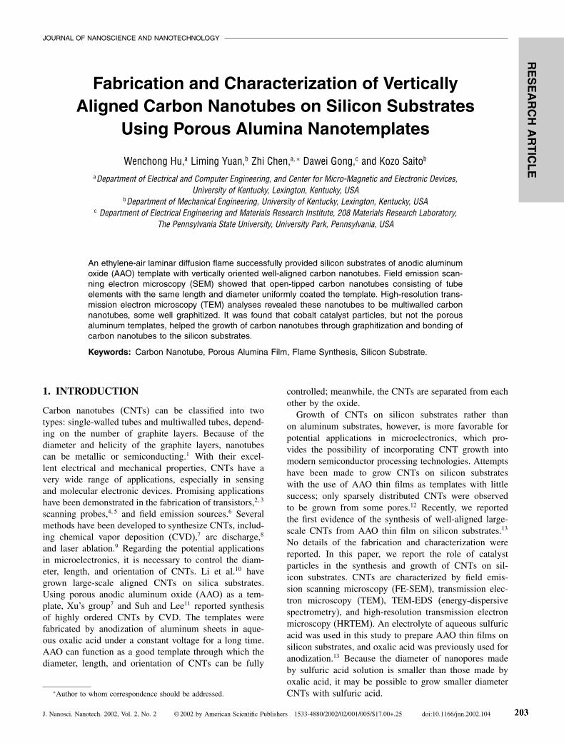
The setup for the flame synthesis, similar to the one usedpreviously,17 is shown in Figure 1. The apparatus consistsof two concentric tubes. The inner tube, made of stainlesssteel, is 1.1 cm in diameter. The outer tube is made ofcopper and has a diameter of 5 cm. Fuel flows through theinner tube at a rate of 4.46 cm3/s, and air flows throughthe annular space between the inner and outer tubes at arate of 1176 cm3/s. The fuel used is a chemically pure(CP) grade ethylene of 99.5% purity. A steady and sta-ble laminar diffusion flame with a visible flame height of33 mm is established on the burner port.The experimental results show that the position in the
flame suitable for synthesis of CNTs is about 4 mm abovethe burner exit. The flame diameter at this location isabout 10 mm. The AAO template (10 mm × 5 mm) wasinserted into the flame perpendicular to the gas flow direc-tion and kept in place for 20 min. The pyrolysized gaseousproducts were impinged on the template. With the heat
QUARTZ BURNER
X-Y POSITIONER
SAMPLING PROBE
GLASS CHIMNEY FLAME
GLASS BEADS
CATHETOMETER
FUEL
AIR
N 2
THREE-WAYSWITCHING VALVE
CONTROL VALVE
FLOW METER
Fig. 1. A schematic of a flame-synthesis experimental apparatus.
generated at flame sheet, the gas environment near thetemplate was suitable for CNT synthesis with a tempera-ture of 1200–1500 �C. Visual inspections showed a layerof smooth and shiny black material on Sample I; most ofthe thin film layer on Sample II was peeled off, and theremaining parts appeared spongy. This shows that with-out cobalt catalyst (Sample II), CNTs do not adhere wellto the substrate. To observe the CNT arrays inside theAAO pores under SEM, the samples were dipped in thechromic and phosphoric acid mixture to partially removeAAO templates. To prepare samples for TEM analysis, weetched the AAO overnight with aqueous NaOH (0.1 M).Because CNTs in Sample I with cobalt deposition werebonded tightly to the silicon substrate, the substrate hadto be broken into pieces to release CNTs. After severalwashes by ethanol alcohol and dispersion by ultrasoniccleaning for 10 min, drops of CNTs were placed on thecopper TEM grids and dried.
3. RESULTS AND DISCUSSION
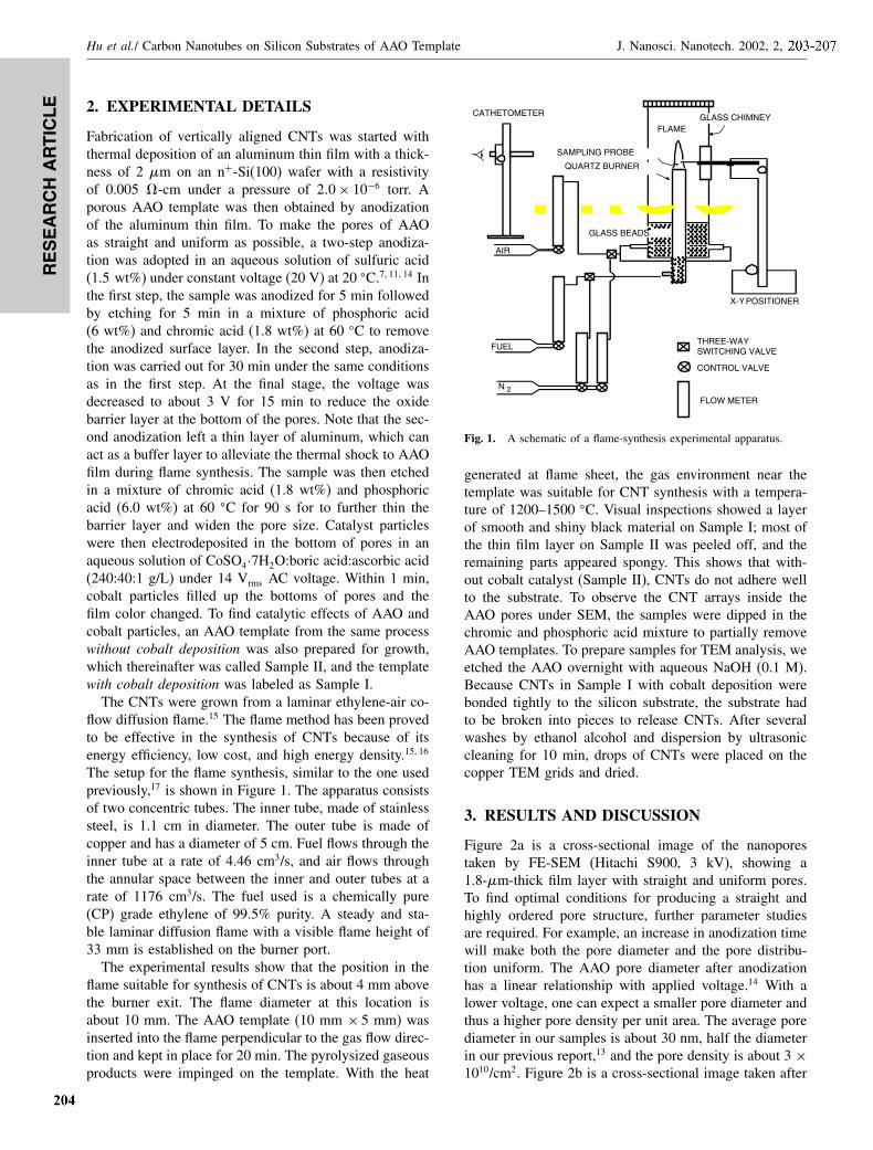
Figure 2a is a cross-sectional image of the nanoporestaken by FE-SEM (Hitachi S900, 3 kV), showing a1.8-�m-thick film layer with straight and uniform pores.To find optimal conditions for producing a straight andhighly ordered pore structure, further parameter studiesare required. For example, an increase in anodization timewill make both the pore diameter and the pore distribu-tion uniform. The AAO pore diameter after anodizationhas a linear relationship with applied voltage.14 With alower voltage, one can expect a smaller pore diameter andthus a higher pore density per unit area. The average porediameter in our samples is about 30 nm, half the diameterin our previous report,13 and the pore density is about 3 ×10¹⁰/cm2. Figure 2b is a cross-sectional image taken after
2
Zhi Chen
Text Box
204
Zhi Chen
Text Box
203-207
RESEARCHARTICLE
J. Nanosci. Nanotech. 2002, 2, 1–5 Hu et al./ Carbon Nanotubes on Silicon Substrates of AAO Template
300nm
(a)
300nm
(b)
Fig. 2. SEM cross-sectional images of AAO nanopores in Sample I.(a) Before Co electrodeposition. (b) After Co electrodeposition.
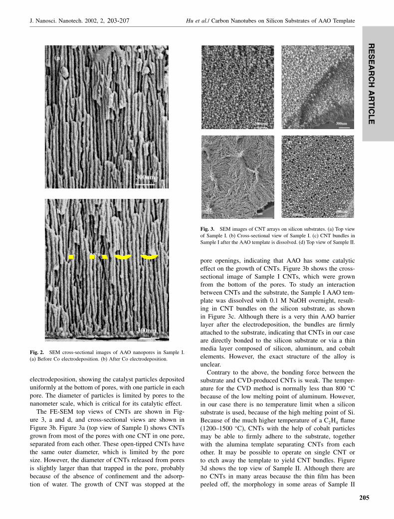
electrodeposition, showing the catalyst particles depositeduniformly at the bottom of pores, with one particle in eachpore. The diameter of particles is limited by pores to thenanometer scale, which is critical for its catalytic effect.The FE-SEM top views of CNTs are shown in Fig-
ure 3, a and d, and cross-sectional views are shown inFigure 3b. Figure 3a (top view of Sample I) shows CNTsgrown from most of the pores with one CNT in one pore,separated from each other. These open-tipped CNTs havethe same outer diameter, which is limited by the poresize. However, the diameter of CNTs released from poresis slightly larger than that trapped in the pore, probablybecause of the absence of confinement and the adsorp-tion of water. The growth of CNT was stopped at the
300nm
(a)
300nm
(b)
300nm
3um
(c)
300nm
(d)
Fig. 3. SEM images of CNT arrays on silicon substrates. (a) Top viewof Sample I. (b) Cross-sectional view of Sample I. (c) CNT bundles inSample I after the AAO template is dissolved. (d) Top view of Sample II.
pore openings, indicating that AAO has some catalyticeffect on the growth of CNTs. Figure 3b shows the cross-sectional image of Sample I CNTs, which were grownfrom the bottom of the pores. To study an interactionbetween CNTs and the substrate, the Sample I AAO tem-plate was dissolved with 0.1 M NaOH overnight, result-ing in CNT bundles on the silicon substrate, as shownin Figure 3c. Although there is a very thin AAO barrierlayer after the electrodeposition, the bundles are firmlyattached to the substrate, indicating that CNTs in our caseare directly bonded to the silicon substrate or via a thinmedia layer composed of silicon, aluminum, and cobaltelements. However, the exact structure of the alloy isunclear.Contrary to the above, the bonding force between the
substrate and CVD-produced CNTs is weak. The temper-ature for the CVD method is normally less than 800 �Cbecause of the low melting point of aluminum. However,in our case there is no temperature limit when a siliconsubstrate is used, because of the high melting point of Si.Because of the much higher temperature of a C2H4 flame(1200–1500 �C), CNTs with the help of cobalt particlesmay be able to firmly adhere to the substrate, togetherwith the alumina template separating CNTs from eachother. It may be possible to operate on single CNT orto etch away the template to yield CNT bundles. Figure3d shows the top view of Sample II. Although there areno CNTs in many areas because the thin film has beenpeeled off, the morphology in some areas of Sample II
3
Zhi Chen
Text Box
205
Zhi Chen
Text Box
203-207
RESEARCHARTICLE
Hu et al./ Carbon Nanotubes on Silicon Substrates of AAO Template J. Nanosci. Nanotech. 2002, 2, 1–5
is almost the same as that of Sample I. Note that CNTsin Sample II had a weak bond to the substrate; accord-ingly, after etching overnight in 0.1 M NaOH, all of theCNTs were separated from the substrate. This indicatesthat cobalt particles help CNTs bond to the substrate.TEM characterization was carried out with a JEM-
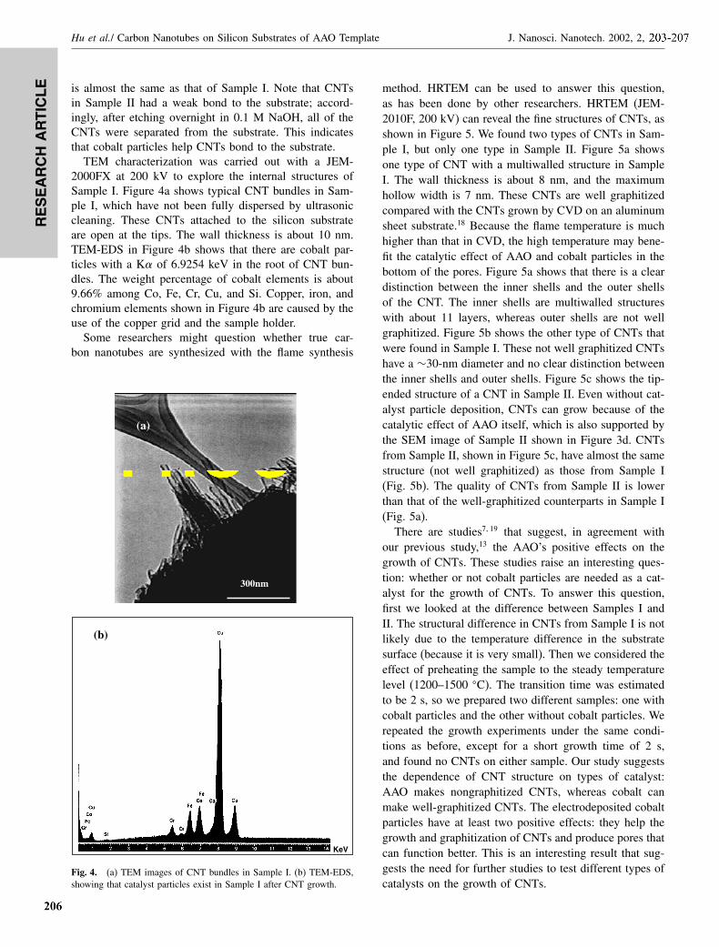
2000FX at 200 kV to explore the internal structures ofSample I. Figure 4a shows typical CNT bundles in Sam-ple I, which have not been fully dispersed by ultrasoniccleaning. These CNTs attached to the silicon substrateare open at the tips. The wall thickness is about 10 nm.TEM-EDS in Figure 4b shows that there are cobalt par-ticles with a K� of 6.9254 keV in the root of CNT bun-dles. The weight percentage of cobalt elements is about9.66% among Co, Fe, Cr, Cu, and Si. Copper, iron, andchromium elements shown in Figure 4b are caused by theuse of the copper grid and the sample holder.Some researchers might question whether true car-
bon nanotubes are synthesized with the flame synthesis
300nm
(a)
(b)
KeV
Fig. 4. (a) TEM images of CNT bundles in Sample I. (b) TEM-EDS,showing that catalyst particles exist in Sample I after CNT growth.
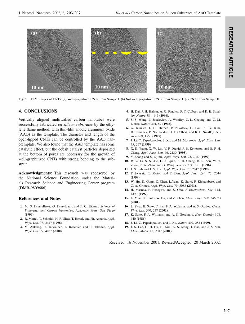
method. HRTEM can be used to answer this question,as has been done by other researchers. HRTEM (JEM-2010F, 200 kV) can reveal the fine structures of CNTs, asshown in Figure 5. We found two types of CNTs in Sam-ple I, but only one type in Sample II. Figure 5a showsone type of CNT with a multiwalled structure in SampleI. The wall thickness is about 8 nm, and the maximumhollow width is 7 nm. These CNTs are well graphitizedcompared with the CNTs grown by CVD on an aluminumsheet substrate.18 Because the flame temperature is muchhigher than that in CVD, the high temperature may bene-fit the catalytic effect of AAO and cobalt particles in thebottom of the pores. Figure 5a shows that there is a cleardistinction between the inner shells and the outer shellsof the CNT. The inner shells are multiwalled structureswith about 11 layers, whereas outer shells are not wellgraphitized. Figure 5b shows the other type of CNTs thatwere found in Sample I. These not well graphitized CNTshave a ∼30-nm diameter and no clear distinction betweenthe inner shells and outer shells. Figure 5c shows the tip-ended structure of a CNT in Sample II. Even without cat-alyst particle deposition, CNTs can grow because of thecatalytic effect of AAO itself, which is also supported bythe SEM image of Sample II shown in Figure 3d. CNTsfrom Sample II, shown in Figure 5c, have almost the samestructure (not well graphitized) as those from Sample I(Fig. 5b). The quality of CNTs from Sample II is lowerthan that of the well-graphitized counterparts in Sample I(Fig. 5a).There are studies7�19 that suggest, in agreement with
our previous study,13 the AAO’s positive effects on thegrowth of CNTs. These studies raise an interesting ques-tion: whether or not cobalt particles are needed as a cat-alyst for the growth of CNTs. To answer this question,first we looked at the difference between Samples I andII. The structural difference in CNTs from Sample I is notlikely due to the temperature difference in the substratesurface (because it is very small). Then we considered theeffect of preheating the sample to the steady temperaturelevel (1200–1500 �C). The transition time was estimatedto be 2 s, so we prepared two different samples: one withcobalt particles and the other without cobalt particles. Werepeated the growth experiments under the same condi-tions as before, except for a short growth time of 2 s,and found no CNTs on either sample. Our study suggeststhe dependence of CNT structure on types of catalyst:AAO makes nongraphitized CNTs, whereas cobalt canmake well-graphitized CNTs. The electrodeposited cobaltparticles have at least two positive effects: they help thegrowth and graphitization of CNTs and produce pores thatcan function better. This is an interesting result that sug-gests the need for further studies to test different types ofcatalysts on the growth of CNTs.
4
Zhi Chen
Text Box
206
Zhi Chen
Text Box
203-207
RESEARCHARTICLE
J. Nanosci. Nanotech. 2002, 2, 1–5 Hu et al./ Carbon Nanotubes on Silicon Substrates of AAO Template
(a) (b)
10 nm 10 nm
(c)
10 nm
Fig. 5. TEM images of CNTs. (a) Well-graphitized CNTs from Sample I. (b) Not well graphitized CNTs from Sample I. (c) CNTs from Sample II.
4. CONCLUSIONS
Vertically aligned multiwalled carbon nanotubes weresuccessfully fabricated on silicon substrates by the ethy-lene flame method, with thin-film anodic aluminum oxide(AAO) as the template. The diameter and length of theopen-tipped CNTs can be controlled by the AAO nan-otemplate. We also found that the AAO template has somecatalytic effect, but the cobalt catalyst particles depositedat the bottom of pores are necessary for the growth ofwell-graphitized CNTs with strong bonding to the sub-strate.
Acknowledgments: This research was sponsored bythe National Science Foundation under the Materi-als Research Science and Engineering Center program(DMR-9809686).
References and Notes
1. M. S. Dresselhaus, G. Dreselhaus, and P. C. Eklund, Science ofFullerenes and Carbon Nanotubes, Academic Press, San Diego(1996).
2. R. Martel, T. Schmidt, H. R. Shea, T. Hertel, and Ph. Avouris, Appl.Phys. Lett. 73, 2447 (1998).
3. M. Ahlskog, R. Tarkiainen, L. Roschier, and P. Hakonen, Appl.Phys. Lett. 77, 4037 (2000).
4. H. Dai, J. H. Hafner, A. G. Rinzler, D. T. Colbert, and R. E. Smal-ley, Nature 384, 147 (1996).
5. S. S. Wong, E. Joselevich, A. Woolley, C. L. Cheung, and C. M.Lieber, Nature 394, 52 (1998).
6. G. Rinzler, J. H. Hafner, P. Nikolaev, L. Lou, S. G. Kim,D. Tomanek, P. Nordlander, D. T. Colbert, and R. E. Smalley, Sci-ence 269, 1550 (1995).
7. J. Li, C. Papadopoulos, J. Xu, and M. Moskovits, Appl. Phys. Lett.75, 367 (1999).
8. X. K. Wang, X. W. Lin, V. P. Dravid, J. B. Ketterson, and E. P. H.Chang, Appl. Phys. Lett. 66, 2430 (1995).
9. Y. Zhang and S. Lijima, Appl. Phys. Lett. 75, 3087 (1999).10. W. Z. Li, S. S. Xie, L. X. Qian, B. H. Chang, B. S. Zou, W. Y.
Zhou, R. A. Zhao, and G. Wang, Science 274, 1701 (1996).11. J. S. Suh and J. S. Lee, Appl. Phys. Lett. 75, 2047 (1999).12. T. Iwasaki, T. Motoi, and T. Den, Appl. Phys. Lett. 75, 2044
(1999).13. W. Hu, D. Gong, Z. Chen, L.Yuan, K. Saito, P. Kichambare, and
C. A. Grimes, Appl. Phys. Lett. 79, 3083 (2001).14. H. Masuda, F. Hasegwa, and S. Ono, J. Electrochem. Soc. 144,
L127 (1997).15. L. Yuan, K. Saito, W. Hu, and Z. Chen, Chem. Phys. Lett. 346, 23
(2001).16. L. Yuan, K. Saito, C. Pan, F. A. Williams, and A. S. Gordon, Chem.
Phys. Lett. 340, 237 (2001).17. K. Saito, F. A. Williams, and A. S. Gordon, J. Heat Transfer 108,
640 (1986).18. J. Li, C. Papadopoulos, and J. Xu, Nature 402, 253 (1999).19. J. S. Lee, G. H. Gu, H. Kim, K. S. Jeong, J. Bae, and J. S. Suh,
Chem. Mater. 13, 2387 (2001).
Received: 16 November 2001. Revised/Accepted: 20 March 2002.