Page 1
Facilitating FPGA Reconfiguration through Low-level Manipulation
Wenwei Zha
Dissertation submitted to the Faculty of the Virginia Polytechnic Institute and
State University in partial fulfillment of the requirements for the degree of
Doctor of Philosophy
in
Electrical Engineering
Peter M. Athanas, Chair
Paul E. Plassmann
Joseph G. Tront
Patrick R. Schaumont
Shu-Ming Sun
Feb 20, 2014
Blacksburg, Virginia
Keywords: FPGA Reconfiguration, Bitstream-level Manipulation, FPGA Routing,
Module Reuse, Design Assembly, Autonomous Adaptive Systems, Electronic
Design Automation
Copyright 2014, Wenwei Zha. All Rights Reserved.
Page 2
Facilitating FPGA Reconfiguration through Low-level Manipulation
Wenwei Zha
Abstract
The process of FPGA reconfiguration is to recompile a design and then update
the FPGA configuration correspondingly. Traditionally, FPGA design compilation
follows the way how hardware is compiled for achieving high performance, which
requires a long computation time. How to efficiently compile a design becomes
the bottleneck for FPGA reconfiguration.
It is promising to apply some techniques or concepts from software to facilitate
FPGA reconfiguration. This dissertation explores such an idea by utilizing three
types of low-level manipulation on FPGA logic and routing resources, i.e.
relocating, mapping/placing, and routing. It implements an FMA technique for
“fast reconfiguration”. The FMA makes use of the software compilation
technique of reusing pre-compiled libraries for explicitly reducing FPGA
compilation time. Based the software concept of Autonomic Computing, this
dissertation proposes to build an Autonomous Adaptive System (AAS) to achieve
“self-reconfiguration”. An AAS absorbs the computing complexity into itself and
compiles the desired change on its own.
For routing, an FPGA router is developed. This router is able to route the MCNC
Page 3
iii
benchmark circuits on five Xilinx devices within 0.35 ~ 49.05 seconds. Creating
a routing-free sandbox with this router is 1.6 times faster than with OpenPR. The
FMA uses relocating to load pre-compiled modules and uses routing to stitch the
modules. It is an essential component of TFlow, which achieves 8 ~ 39 times
speedup as compared to the traditional ISE flow on various test cases. The core
part of an AAS is a lightweight embedded version of utilities for managing the
system’s hardware functionality. Two major utilities are mapping/placing and
routing. This dissertation builds a proof-of-concept AAS with a universal UART
transmitter. The system autonomously instantiates the circuit for generating the
desired BAUD rate to adapt to the requirement of a remote UART receiver.
Page 4
iv
Acknowledgments
First of all, I would like to thank my academic adviser Dr. Athanas, for leading me
into the world of configurable computing, for funding me through all these years,
for giving me the chances to work on various research projects, for advising me
to try different ideas, and for the patient discussion and enlightening comments
regarding writing this dissertation.
I would like to thank Dr. Schaumont, Dr. Plassmann, Dr. Tront, and Dr. Sun for
being my committee and for the insightful suggestions on how to improve this
dissertation.
Many thanks to the former and present fellows of the Configurable Computing
Lab. Without the foundation built in Dr. Neil Steiner’s dissertation, my work on
the autonomous adaptive systems is not feasible. Dr. Steiner has also been the
main resource for getting help on issues related to TORC. It has been a
pleasure to work with Andre Love on developing TFlow. Thanks to Rohit
Asthana, Jacob Couch, Dr. Tony Frangieh, Dr. Krzysztof Kepa, Ryan Marlow,
Umang Parekh, Dr. Adolfo Reico, Kavya Shagrithaya, Ali Sohanghpurwala,
Richard Stroop, Dr. Jorge Suris, Abhay Tavaragiri and Xin Xin, for all the help
and support.
Page 5
v
Thanks to Dr. Aaron Wood, for helping implement the FPGA router; and to Dr.
Christopher Lavin, for answering my questions regarding RapidSmith.
Last but not least, I cannot thank my family enough. Thanks to my parents for
raising me up and for encouraging me to pursue higher education. Thanks to my
sister, Dr. Wenjuan Zha, and my brother-in-law, Dr. Rudy Gunawan, for their
endless support. Special thanks to my wife, Qian Wang, for her sacrifice,
encouragement, quiet patience, and unwavering love through my PhD journey.
Page 6
vi
Table of Contents
Abstract ................................................................................................................. ii
Acknowledgments ................................................................................................ iv
Table of Contents ................................................................................................. vi
List of Figures ..................................................................................................... viii
List of Tables ........................................................................................................ x
Acronyms and Abbreviations ............................................................................... xi
Glossary .............................................................................................................. xiii
Chapter 1 Introduction ....................................................................................... 1
1.1. Overview .................................................................................................. 1
1.2. Motivation ................................................................................................ 2
1.3. Problem Statement .................................................................................. 5
1.4. Contribution ............................................................................................. 8
1.5. Limitations .............................................................................................. 11
1.6. Organization .......................................................................................... 13
Chapter 2 Background and Related Work ....................................................... 15
2.1. Overview ................................................................................................ 15
2.2. FPGA Architecture and Configuration .................................................... 18
2.3. FPGA Reconfiguration ........................................................................... 23
2.4. FPGA Routing ........................................................................................ 27
2.5. Fast System Prototyping ........................................................................ 34
2.6. Autonomous Adaptive Systems ............................................................. 41
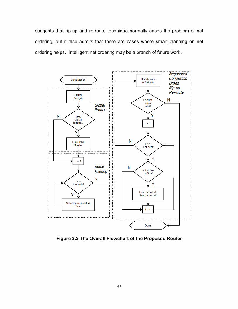
Chapter 3 A Versatile FPGA Router ................................................................ 48
3.1. Routing Graph ....................................................................................... 49
3.2. Overall Flowchart ................................................................................... 51
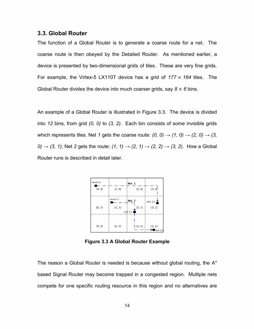
3.3. Global Router ......................................................................................... 54
3.4. Detailed Router ...................................................................................... 57
3.5. Global Planner ....................................................................................... 64
Page 7
vii
3.6. Experiments on Benchmark Circuits ...................................................... 66
3.7. Demonstration Applications ................................................................... 69
3.8. Summary, Conclusion and Future Work .................................................. 73
Chapter 4 Fast Module Assembly .................................................................... 75
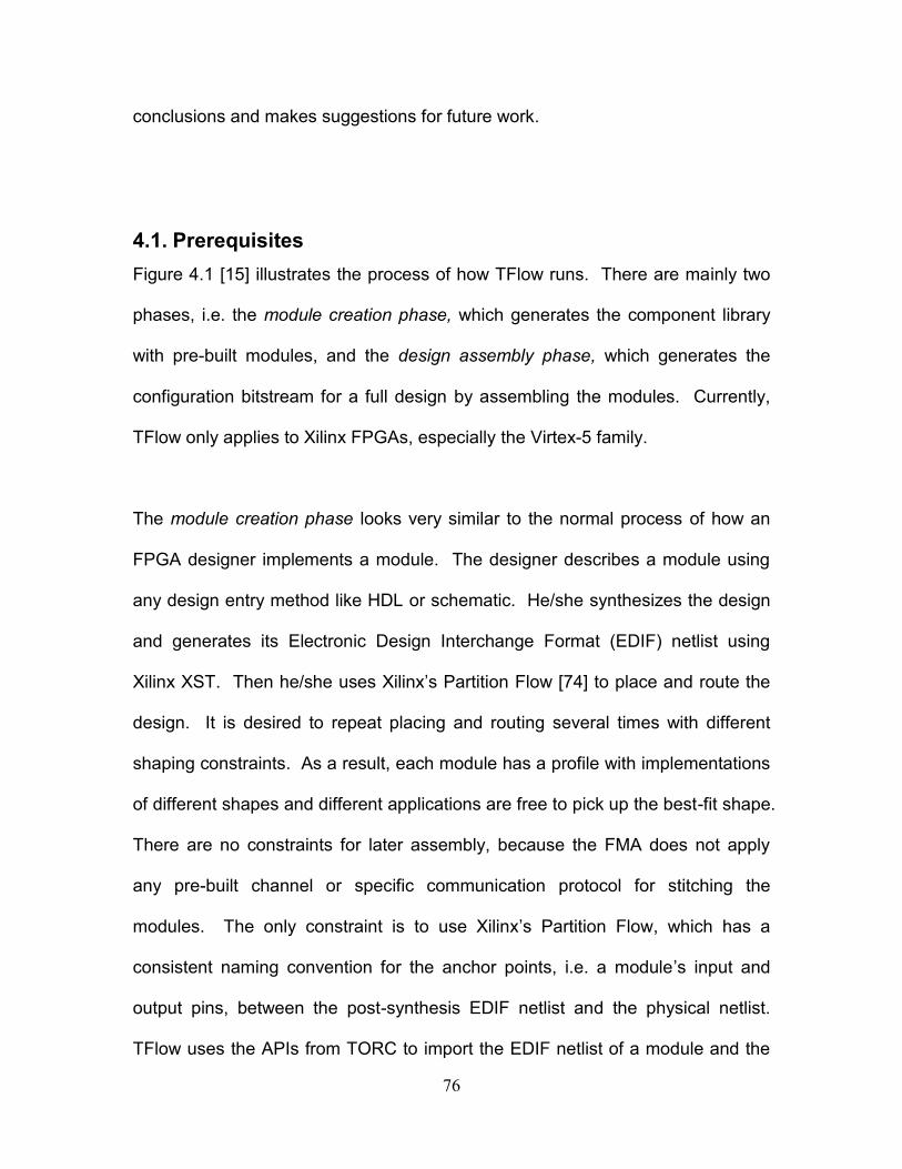
4.1. Prerequisites .......................................................................................... 76
4.2. Module Relocating ................................................................................. 78
4.3. Module Stitching .................................................................................... 84
4.4. Debugging ............................................................................................. 87
4.5. Demonstration and Experiment Result .................................................. 88
4.6. Summary, Conclusion and Future Work .................................................. 95
Chapter 5 Autonomous Adaptive Systems ...................................................... 97
5.1. A Framework for Building an AAS ......................................................... 98
5.2. System Implementation – Hardware .................................................... 100
5.3. System Implementation – Software ..................................................... 102
5.4. Demonstration – A Universal UART Transmitter ................................. 114
5.5. Performance Analysis .......................................................................... 117
5.6. Summary, Conclusion and Future Work ................................................ 121
Chapter 6 Conclusion .................................................................................... 124
Reference ......................................................................................................... 126
Appendix A Publication List .............................................................................. 138
Page 8
viii
List of Figures
Figure 2.1 Background Overview ................................................................................ 18
Figure 2.2 A Simplified FPGA Architecture ................................................................ 19
Figure 2.3 The Simplified Block Diagram of the Xilinx XC4000 CLB ..................... 19
Figure 2.4 The Programmable Interconnect of the Xilinx XC4000 Device ........... 20
Figure 2.5 The Comparison between the Slot-based and the Non-slot-based
Reconfiguration............................................................................................................... 27
Figure 2.6 A Typical Model of the FPGA Routing Problem ..................................... 28
Figure 2.7 A Simplified FPGA Routing Graph ........................................................... 32
Figure 2.8 A Simplified Diagram of An AAS .............................................................. 41
Figure 3.1 A Simplified Example of the Routing Graph Extracted from XDLRC .. 50
Figure 3.2 The Overall Flowchart of the Proposed Router ...................................... 53
Figure 3.3 A Global Router Example .......................................................................... 54
Figure 3.4 The Flowchart of the Detailed Router ...................................................... 58
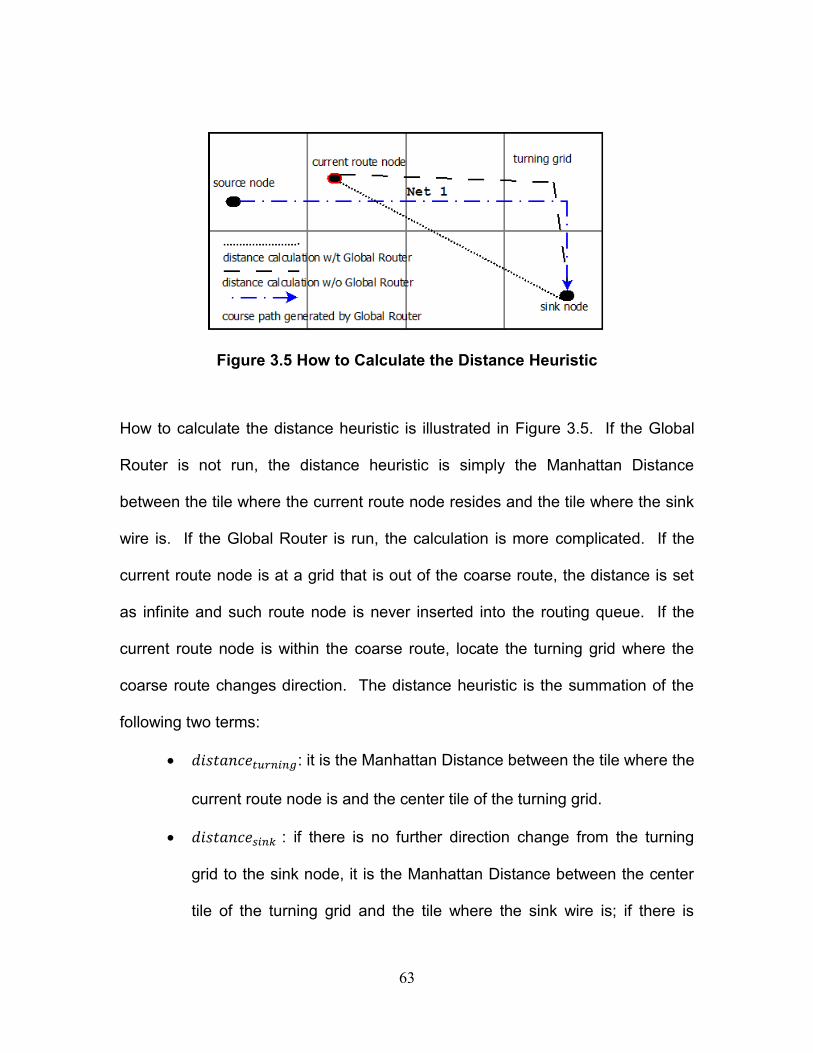
Figure 3.5 How to Calculate the Distance Heuristic ................................................. 63
Figure 3.6 The Routing-free Sandbox Creation for A Video Filter Design ............ 70
Figure 3.7 The Routing-free Sandbox Creation for Bigger Designs ...................... 72
Figure 4.1How TFlow Runs .......................................................................................... 77
Figure 4.2 How to Divide a 32-bit Frame Address into Six Fields .......................... 78
Figure 4.3 The Top/Botoom Bit and the Raw Address in Xilinx FPGA.................. 79
Figure 4.4 The Assignment of Major Addresses in a Major Row ........................... 80
Figure 4.5 How the Bitstream Level Module Relocation Works ............................. 81
Page 9
ix
Figure 4.6 Applying the FMA for a GNU Radio System Development .................. 88
Figure 5.1 A Framework for Building an AAS ............................................................ 98
Figure 5.2 Hardware Components of the Demonstration AAS ............................. 101
Figure 5.3 The Flowchart of the Greedy Placer ...................................................... 107
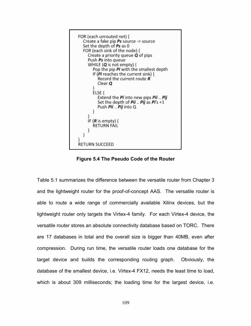
Figure 5.4 The Pseudo Code of the Router ............................................................. 109
Figure 5.5 How the Demonstration AAS Adapts ..................................................... 117
Page 10
x
List of Tables
Table 3.1 The Runtime of Routing the MCNC Benchmark Circuits on Different
Devices (in Seconds) .......................................................................................... 67
Table 4.1 The Exact Number of Frames per Column.......................................... 81
Table 4.2 The Resource Utilization Comparison (The Full Design) .................... 91
Table 4.3 Design Compilation (Back-end) Time Comparison ............................. 92
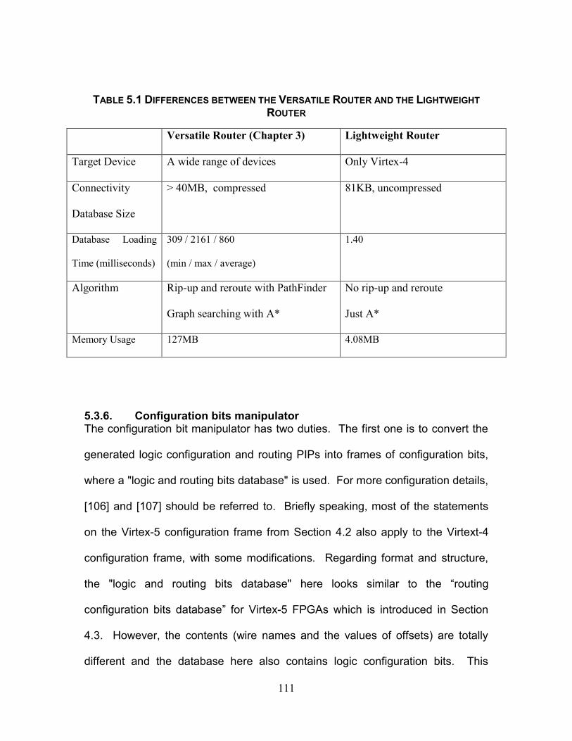
Table 5.1 Differences between the Versatile Router and the Lightweight Router
.......................................................................................................................... 111
Table 5.2 The Implementation Run Time Comparison ...................................... 118
Table 5.3 The Performance Comparison .......................................................... 119
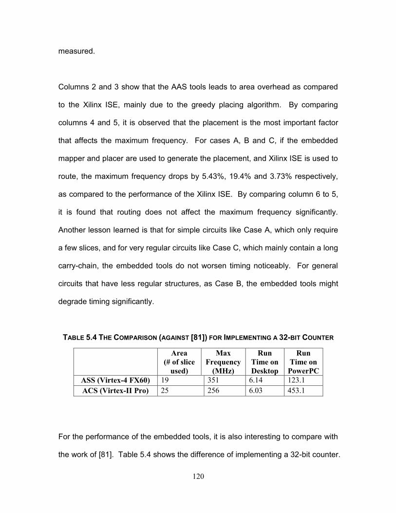
Table 5.4 The Comparison for Implementing a 32-bit Counter ......................... 120
Page 11
xi
Acronyms and Abbreviations
AAS Autonomous Adaptive System
ADB Alternative Wire Database
API Application Programming Interface
ASIC Application Specific Integrated Circuit
BFS Breadth First Search
BIP Bitstream Intellectual Property
BLIF Berkeley Logic Interchange Format
BRAM Block Random Access Memory
BSB Base System Builder
CAD Computer-Automated Design
CLB Configurable Logic Block
DPR Dynamic Partial Reconfiguration
DSP Digital Signal Processing
EDA Electronic Design Automation
EDIF Electronic Design Interchange Format
EDK Embedded Development Kit
ELDK Embedded Linux Development Kit
FAR Frame Address Register
FMA Fast Module Assembly
FPGA Field-Programmable Gate Array
Page 12
xii
GUI Graphical User Interface
HCLK Horizontal Clock
HDL Hardware Description Language
HLS High Level Synthesis
IC Integrated Circuit
ICAP Internal Configuration Access Port
IOB Input/Output Block
IP Intellectual Property
ISE Integrated Software Environment
JVM Java Virtual Machine
NFS Network File System
PIP Programmable Interconnection Point
PR Partial Reconfiguration
PSM Programmable Switch Matrix
RBN Random Boolean Networks
ROCR Riverside On-Chip Router
SA Simulated Annealing
SAT Boolean Satisfiability
TMR Triple Modular Redundancy
TORC Tools for Open Reconfigurable Computing
XDL Xilinx Design Language
XDLRC Architecture Description for Xilinx Devices
Page 13
xiii
Glossary
arc A connection between two wires.
bitgen The Xilinx utility to generate the configuration bitstream for its
FPGA devices.
.bit The Xilinx file extension for its configuration bitstream file.
bitstream Equivalent to configuration bitstream – the binary data that is
suitable for download into a device to program it.
EDIF A vendor-neutral format store Electronic netlists and schematics.
EDK The Xilinx GUI tool suite for generating microprocessor-based
designs that are embedded inside FPGAs.
HDL A textual language to describe the structure, design and
operation of an electronic (normally digital) circuit.
IP A product of the human intellect that the law protects from
unauthorized use by others. An IP core in electronics refers to a
reusable unit of design that is the IP of one party.
ISE The Xilinx tool suite for compiling and programming an FPGA
design, including various utilities for design entry, synthesis,
mapping, placing, routing, timing analysis, bistream generating,
configuring, etc.
JVM The virtual machine used for the execution of compiled Java
programs.
Page 14
xiv
Mapper In general, a mapper is a tool to map a generic logic gate such as
AND, OR, and NOT to a technology specific gate. However, in
this dissertation, the mapper actually means the packer, which is
a tool for packing the primitive gates into one or a few primate
sites (such as SLICE) for an FPGA device.
Module One or a set of parts that can be connected or combined to build
an electronic design.
.ncd The Xilinx file extension for its physical netlist in the NCD (Native
Circuit Description) format, which is not human-readable.
Net A net is a connection in a netlist connecting two logic
components.
Netlist A combination of logic components and the connections between
them for describing an electronic design. In a logic netlist, the
logic components are generic logic gates and the nets are
abstract connections. In a physical netlist, the logic components
are primitive sites of an FPGA device and the connections are
electrical nodes in the form of a set of PIPs.
NP-Hard Non-deterministic Polynomial-time hard. In practice, an NP-hard
problem cannot be solved in a deterministic way in polynomial
time. Its exact solution can be acquired through the exhaustive
search, but that may consume impractical computing time and
resources.
par The Xilinx tool to perform the functions of a placer and a router.
Page 15
xv
Placer A tool to allocate optimal locations for the mapped and packed
primitive sites, in the form of resource instances for a give FPGA
device.
Router A tool to make the optimal connections between the placed
primitive sites for a target device.
QFlow Quick Flow, an accelerated FPGA compilation flow, which reuses
pre-compiled fully-placed modules.
Synthesizer A tool to convert HDL files into Boolean equations, to optimize
these equations, and to map them to generic logic gates.
Tflow Turbo Flow, an instant FPGA compilation flow, which reuses the
configuration bitstream of pre-compiled modules.
WoD Wires on Demand. A run-time framework to implement and
configure inter-module connections for certain Xilinx FPGA
devices.
.xdl The Xilinx file extension for its physical netlist in the XDL format.
An .xdl netlist and an .ncd netlist can be translated to each other
through Xilinx utility xdl.
Page 16
1
Chapter 1
Introduction
1.1. Overview
A Field-programmable Gate Array (FPGA) is a special type of Integrated Circuit
(IC) devices. Instead of performing a specific functionality, the hardware
configuration of an FPGA can be reconfigured repeatedly to serve different
applications. FPGA reconfiguration is the process to compile a new design and
to generate the corresponding configuration binaries for programming the target
FPGA device. This process is becoming more and more challenging with the
growth of FPGA device density and FPGA design complexity. To facilitate FPGA
reconfiguration, this dissertation proposes “fast reconfiguration” and “self-
reconfiguration”. For “fast reconfiguration”, a Fast Module Assembly (FMA)
approach is implemented based on reusing the configuration bitstream of pre-
built modules. The FMA is an enabling technique for reducing the FPGA design
compilation time. For “self-reconfiguration”, a framework for building an
Autonomous Adaptive System (AAS) is presented. By managing hardware
resources and functionality on its own, an AAS absorbs much of the computing
complexity into itself and avoids extra compilation.
Page 17
2
1.2. Motivation
Since their invention in the middle of 1980s, FPGAs [1] have gained increasing
success in various markets including digital signal processing, embedded
microprocessor applications, physical layer communications and reconfigurable
computing [2]. One main reason for FPGAs’ popularity is that they take
advantage of the Application Specific IC (ASIC) based and the general purpose
processor based designs [3]. On the one hand, FPGAs provide the hardware
performance and reliability of an ASIC design. On the other hand, FPGAs also
offer the software reconfigurability and flexibility of a general purpose processor
based design. Traditionally, the FPGA tool chain puts too much emphasis on the
first feature, i.e. the hardware performance and reliability. It follows the process
of compiling ASIC designs, which consists of a series of NP-hard problems [4, 5].
This process needs a long time to run for optimizing area and maximum
operating frequency. It also requires vast computation power typically from
personal or workstation computers. In contrast, the second feature, i.e. the
software reconfigurability and flexibility, has attracted relatively less attention.
How to fully exploit this feature leads to the topic of facilitating FPGA
reconfiguration.
FPGA reconfiguration does not merely mean the feasibility of reprogramming an
FPGA device after recompiling the target design. It is the full process from
compiling a new design into the physical netlist, to generate the configuration
Page 18
3
binaries, and to program the target device1. The process also calls for efficiency
and flexibility. Because of the limitations of the traditional tools mentioned above,
the bottleneck here is still the time and effort required for compiling an FPGA
design – an essentially NP-hard problem. Following Moore’s Law, the density of
FPGAs keeps growing exponentially from thousands of kilo-transistors to a few
billion transistors per device. Consequently FPGA designs keep increasing in
size and complexity, which worsens the problem of compiling an FPGA design.
As a result, FPGA reconfiguration is becoming more and more challenging.
To help overcome the challenge of FPGA reconfiguration, this dissertation work
presents a direct approach and an indirect approach. The first approach is “fast
reconfiguration”, which directly makes efforts toward reducing the FPGA design
compilation time. An FMA technique is implemented based on reusing the
configuration bitstream of pre-built modules. This technique is inspired by the
software compilation technique of linking pre-compiled libraries at the final
executable generation stage [6]. The second approach is “self-reconfiguration”.
It is indirect because it does not optimize a single compilation run; rather, it
applies the concept of Autonomic Computing [7] to avoid extra compilation. This
approach implements a framework for building an AAS. An AAS is capable of
managing its own hardware functionality in order to adapt to changes. It
autonomously runs an embedded tool set to compile any necessary changes into
hardware configuration and to implement it on-the-fly as adaptation behavior. In
1 The action of reprogramming is only a very narrow definition of FPGA reconfiguration. A wider
definition like this is assumed throughout this dissertation.
Page 19
4
other words, an AAS absorbs much of the computing complexity into itself so that
there is no need to recompile the system externally.
Another motivation behind “fast reconfiguration” and “self-reconfiguration” is to
open new horizons for FPGA based applications. The ultimate goal of “fast
reconfiguration” by FMA is to boost the FPGA design productivity by reducing the
FPGA compilation time significantly. If FPGA designs are compiled as fast as
software designs, FPGAs would become an alternative choice for applications
such as GNU radio which normally favors the pure software implementation. For
“self-reconfiguration”, researchers on autonomous systems have long utilized
software to implement adaptation behaviors, because it is fast and flexible to
reconfigure software. With an on-chip tool set to arbitrarily modify hardware
configuration during runtime, FPGA becomes a good candidate for implementing
an autonomous system, where hardware is no longer static.
Both “fast reconfiguration” and “self-reconfiguration” rely on the low-level
manipulation of FPGA resources. By directly managing the configuration
binaries of the logic and routing resources, it is essentially feasible to alter the
functionality of an FPGA device under software control. To some degree,
altering FPGA functionality is potentially as easy as altering software functionality
and compiling FPGA is potentially as fast as compiling software. Therefore, the
low-level manipulation is one key to ensure the speed and flexibility of FPGA
reconfiguration.
Page 20
5
In short, this dissertation work aims to facilitate FPGA reconfiguration by
manipulating FPGA configuration at a low level. The next section presents the
detailed problem statement.
1.3. Problem Statement
To investigate how the low-level manipulation facilitates FPGA reconfiguration,
there are naturally two questions to ask:
Question I: What kinds of manipulation are desired?
Question II: More importantly, what are the benefits of such manipulation
and how to demonstrate?
The answer to the first question is straightforward. Three types of manipulation
of FPGA resources are exploited:
1) Relocating: relocate the logic and/or routing configuration of a pre-
compiled module to a new location;
2) Mapping and placing: translate the logic elements of a module into
the corresponding logic configuration and place them onto logic sites;
3) Routing: use routing resources to connect given logic sites and
generate the corresponding configuration.
To ensure high speed, the manipulation is low-level, i.e. it directly instantiates the
binaries that configure the FPGA. Consequently, there is no need to generate
Page 21
6
the actual physical netlist2 (which may take a very long time for a big design) or
to translate the physical netlist into configuration bitstream. To help achieve
flexibility, first, the manipulation is fine-grained through managing the minimum
configurable logic and routing resources; and second, manipulation utilities are
able to run on multiple platforms, especially in the embedded environment.
To explore the second question, the first step is to re-examine the conventional
use-models of contemporary FPGAs. In many areas including consumer
electronics, telecommunication appliances, and medical instruments, people
have chosen to use FPGAs because of performance, time to market, cost, and
reliability considerations. Traditionally, all these applications belong to two use
models in general. One is replacing ASICs as the final design solution [8]. The
other is emulating the functionality of an ASIC design for the purpose of
simulation acceleration [9]. In either case, the core task is to prototype a digital
system in an FPGA device and the main challenge is to reduce the design
compilation time. Since modular design [10] has become a standard practice in
many disciplines including digital hardware design, reusing pre-compiled
modules naturally becomes an ideal candidate for reducing FPGA compilation
time. By utilizing the manipulation of “relocating” and “routing” at a low level, an
FMA 3 approach is developed. It is potentially an enabling technique for
significantly reducing FPGA compilation time. It is worth to mention that the FMA
2 At some point, physical netlist is still used for debug purpose, since it is very difficult to directly
debug configuration bitstream.
3 Section 1.5 reveals some details about the limitation of this work.
Page 22
7
is not only fast by directly “relocating” the configuration bitstream of pre-compiled
modules, but it is also flexible. It is flexible on where the pre-compiled modules
may reside by applying the idea of soltless reconfiguration [11]. It is also flexible
on how a module is pre-compiled. There is no constraint about where its
input/output pin should be. There is no need for extra input/output logic to build
inter-module connection channels. The manipulation “routing” which uses a
dedicated FPGA router to build the inter-module connections during assembly on
the fly ensures such flexibility.
With the emergence of Dynamic Partial Reconfiguration (DPR) technique [12] it
is feasible to change part of an FPGA design’s functionality at runtime. This
technique leads to a novel use model of FPGAs, i.e. AASs. Such systems adapt
to environmental changes including external disturbance (such as temperature
fluctuations or communication protocol changes) and/or internal mutation (such
as a defect or time-varying optimizing objectives) with little or no outside
intervention. There are roughly two levels of autonomy. For the lower level of
autonomy, the system makes the adaptation decision on its own about which
kind of adaptation is desired and then picks up the right partial configuration from
a library of pre-compiled adaptation behaviors. For the higher level of autonomy,
the system not only makes the decision by itself, it also autonomously compiles
the desired adaptation behavior into FPGA configuration binaries and instantiate
it. This dissertation work presents a framework for building an AAS based upon
a minimal set of requirements, namely an FPGA and a modest amount of
Page 23
8
external memory. The highlight of the framework is a lightweight embedded
version of utilities to convert a circuit netlist describing the adaptation behavior
into real FPGA hardware configuration in order to achieve the higher level of
autonomy. Two key components of the utilities is the manipulation of “mapping
and placing” and “routing”.
To sum up the targeting problems and the proposed solutions, this dissertation
work deals with three tasks:
Task I: Invent a versatile FPGA router.
Task II: Propose an FMA technique.
Task III: Develop a framework for building an AAS.
Details about these tasks, i.e. implementation, demonstration, results, etc., are
discussed in Chapter 3, 4, and 5, respectively.
1.4. Contribution
By investigating the two questions and by accomplishing the three tasks
mentioned in the previous section, this dissertation makes the following
contributions:
1. This dissertation exploits the low-level manipulation of FPGA
configuration to facilitate FPGA reconfiguration, i.e. to achieve flexibility by
managing the minimal configurable logic and routing resources, and to
ensure the speed of reconfiguration by directly manipulating the
configuration binaries. To demonstrate this idea, the dissertation
Page 24
9
proposes two techniques for facilitating FPGA reconfiguration, i.e. “fast
reconfiguration” and “self-reconfiguration”.
2. This dissertation develops an FPGA router with the following
features. Instead of targeting a specific device or a family of devices or
some special customized devices, this router targets a wide range of
commercially available FPGA devices. It does not make any architecture-
specific or application-specific simplifications or assumptions, so that it is
able to route different kinds of circuits. It applies the well-accepted
PathFinder [13] algorithm with A* search [14] in order to handle complex
routing. It produces routing results in the real device format which can be
directly applied to FPGA reconfiguration. Most existing FPGA routers only
implement a portion of these features but not all of them. With these
features, this router is an ideal candidate for various FPGA reconfiguration
applications, such as the FMA technique and the AAS framework
developed in this dissertation.
3. This dissertation proposes an FMA technique by combining the
speed advantage of the configuration bitstream level module assembly
and the flexibility advantage of the slotless reconfiguration. The FMA is
faster than the physical netlist based module assembly adopted by recent
work on the slotless reconfiguration without the configuration binary
capability. The FMA is also flexible and its flexibility has two meanings.
First, it is more flexible than the early work on the slot-based bitstream
level module relocation where any change in the design may lead to the
Page 25
10
re-compilation of most of the modules. Second, it applies less constraint
on how modules are pre-compiled as compared to the recent work on the
configuration bitstream based slotless reconfiguration. Modules may be of
any shape, their I/O pins may locate on the boundary or deep inside, and
they may use any routing resources. The FMA is an enabler for the
configuration bitstream level module reuse which helps to significantly
reduce FPGA compilation time. It also potentially enables software-like
exploration for hardware: many design iterations per day, easy debug, etc.
4. This dissertation explores an alternative way to implement
autonomous computing, i.e. through hardware. Early work only focuses
on software where hardware is static and hardware only denotes to
computers with proper peripherals for running software. FPGA
reconfiguration makes hardware autonomy feasible, but the research is
still in an early stage. This dissertation adds value to this area in the
following ways: it proposes a framework for building an autonomous
system with limited resources so that the system is suitable for the
embedded environment; it demonstrates how hardware autonomy is
achieved through the low-level manipulation of FPGA configuration; and it
develops a proof-of-concept autonomous system with an adaptive UART
transmitter.
5. This dissertation develops utilities that run in the embedded
environment to manage the FPGA logic and routing resources at a low
level. Most tools from the literature rely on vendors' utilities at some point,
Page 26
11
for example to generate the physical netlist or to generate the
configuration binaries. Therefore, they lack the flexibility to run in the
embedded environment. To fill in such a gap, this dissertation implements
a tool set for translating digital logics into FPGA configuration within the
autonomous adaptive system framework. It makes some dedicated
manipulations on the placer and the router for fitting the embedded
environment. The placer applies a greedy algorithm with linear runtime
and abandons the popular Simulation Annealing algorithm [5]. The router
applies a few simplifications as compared to the versatile router: first, the
routing database is compact by removing redundancies; second, non-
iterative A* method is used instead of the PathFinder. Developed in C++,
the module assembly technique can also be cross-compiled into an
embedded version with limited effort.
1.5. Limitations
This section briefly talks about a few limitations of this work.
First, the router does not have an accurate wire delay model. While the timing
information for logic elements of a specific FPGA device is found in the device’s
datasheet, the wire delay information is not released. Ideally, a router should be
timing-aware by directly minimizing the overall wire delay; but the router here
only optimizes timing indirectly by minimizing the routing depth.
Page 27
12
Second, the FMA has a few limitations. Module assembly is only the last step of
a complete compilation flow through module reuse. Other steps include: building
and manage the library with pre-compiled modules, selecting the most suitable
module, and placing the module. This dissertation only focuses on the assembly
step. It is part of [15], which discusses a whole compilation flow. Also, details
about how to manage the intermediate meta-data through XML are omitted in
this dissertation and they are found in [16, 17]. Moreover, reducing compilation
time by reusing pre-compiled modules essentially trades compilation quality for
run time. Compared to compiling the full design, the pre-compiled modules
freezes a large portion of the solution space and the globally optimal solution
may become unreachable. [18] discusses details about this trade-off.
Third, the primary objective of the AAS work is to be proof-of-concept,
constrained by a short development time and limited resources in the embedded
environment. It does not exploit the state-of-the-art techniques in dynamic partial
reconfiguration, placing algorithms or routing algorithms. Instead, it makes
simplified implementations here and there. Consequently, head-to-head
quantitative comparison with peer’s work is limited in availability and utility.
Forth, the low-level manipulation on configuration binaries is based on the
unpublished work by the Configurable Computing Labs of Virginia Tech and
Brigham Young University. It has the complete knowledge of all the routing
configuration bits of Xilinx Virtex-4 and Virtex-5 devices as well as most of the
Page 28
13
logic configuration bits of Virtex-4 and Virtex-5. Recent work such as [19] may
be used to acquire similar knowledge about configuration bitstream, but that work
is only applicable to a much coarser granularity than the manipulation here. As a
result, even though in theory this dissertation work may apply to FPGA devices
newer than Virtex-4 and Virtex-5, it may not be feasible in practice.
1.6. Organization
The remainder of this dissertation is organized into the following chapters:
Chapter 2: Background and Related Work
This chapter reviews the preliminary knowledge as well as the peers’ work
representing the state of the art, including FPGA architecture and configuration,
FPGA reconfiguration, FPGA routing, fast system prototyping, and autonomous
adaptive systems.
Chapter 3: A Versatile FPGA router
This chapter discusses the data structure and algorithms for developing the
router as well as the experiment results on the well accepted MCNC benchmark
circuits, and a demonstration of how to generate a routing-free sandbox.
Chapter 4: Fast Module Assembly.
This chapter presents the implementation details of the FMA technique and
proves its significances through quantitative results.
Page 29
14
Chapter 5: Autonomous Adaptive Systems
This chapter shows the details about the framework for building an AAS,
including the details of software implementation and hardware implementation. It
also has a demonstration of a universal UART transmitter as well as limited
quantitative analysis on the performance and characteristics of the embedded
tool set.
Chapter 6: Conclusion
This chapter summarizes the main conclusions of this dissertation.
Page 30
15
Chapter 2
Background and Related Work
2.1. Overview
The foundation of this dissertation depends on a wide range of preliminary
knowledge and related work. It is split into five topics: FPGA architecture and
configuration, FPGA reconfiguration, FPGA routing, fast system prototyping and
autonomous adaptive systems. Each topic will be reviewed regarding the
following aspects:
1. What is the preliminary knowledge and what incentives (capabilities
and/or challenges) does it offer?
2. What existing works are related to this dissertation; what are the
similarities and/or differences between this dissertation and related
works?
3. What are the strengths of this work as compared with related work4?
Figure 2.1 serves as an overview and the detailed review will be presented later.
4 In most cases, head-to-head comparison with quantitative analysis is either difficult to make or
of limited utility. The reason is that most works do not necessarily have exactly the same problem
domain, resource constraint, and premise for solution. This background section mainly makes
qualitative comparison with the related work and later sections will make quantitative
comparisons with selected works.
Page 33
18
Figure 2.1 Background Overview
2.2. FPGA Architecture and Configuration
The popular island style FPGA architecture is illustrated by Figure 2.2 [20]. CLB
refers to Configurable Logic Block and PSM refers to Programmable Switch
Matrix. CLBs contain various logic elements such as Look-Up Tables (LUTs),
Flip-flops (FFs) and dedicated multiplexers (MUXs). PSMs consist of
programmable interconnection points (PIPs). One CLB is connected to another
CLB through one or more PSMs. These terms are from Xilinx FPGAs, but they
may apply to devices from other vendors as well. The insights of the CLB and
PSM of the Xilinx XC4000 FPGA family are shown in Figure 2.3 and 2.4,
respectively.
Page 34
19
Figure 2.2 A Simplified FPGA Architecture [20]
Figure 2.3 The Simplified Block Diagram of the Xilinx XC4000 CLB [20]
Page 35
20
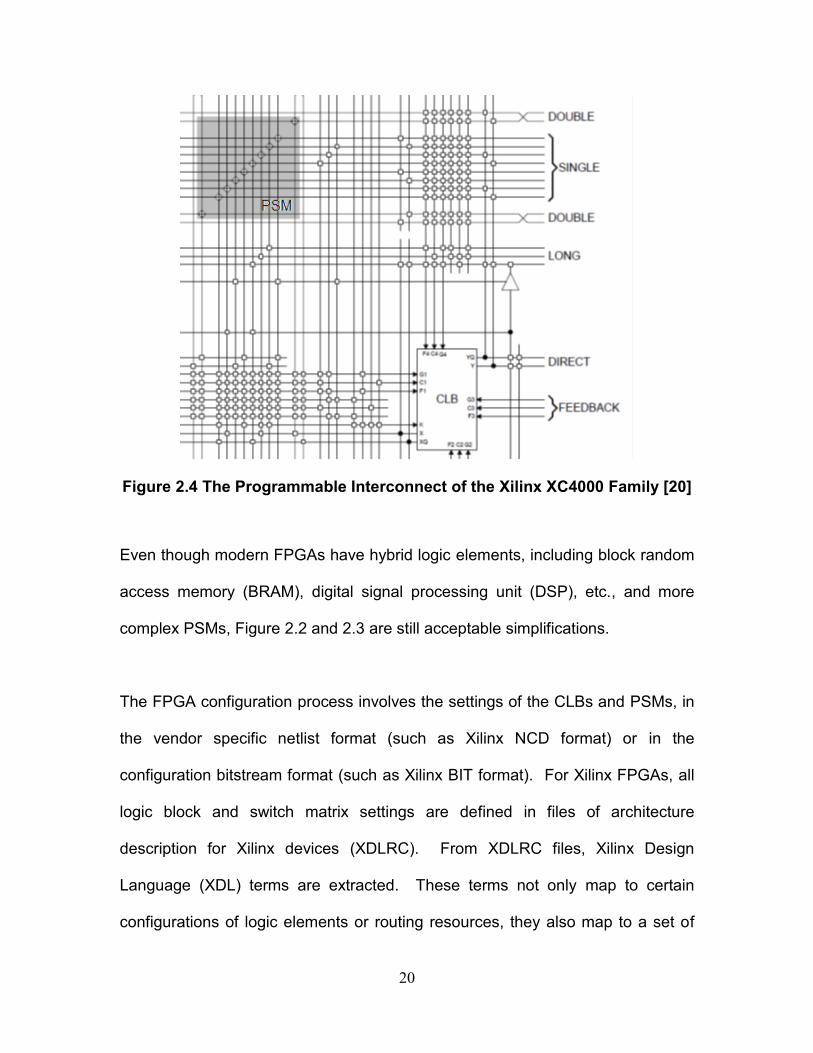
Figure 2.4 The Programmable Interconnect of the Xilinx XC4000 Family [20]
Even though modern FPGAs have hybrid logic elements, including block random
access memory (BRAM), digital signal processing unit (DSP), etc., and more
complex PSMs, Figure 2.2 and 2.3 are still acceptable simplifications.
The FPGA configuration process involves the settings of the CLBs and PSMs, in
the vendor specific netlist format (such as Xilinx NCD format) or in the
configuration bitstream format (such as Xilinx BIT format). For Xilinx FPGAs, all
logic block and switch matrix settings are defined in files of architecture
description for Xilinx devices (XDLRC). From XDLRC files, Xilinx Design
Language (XDL) terms are extracted. These terms not only map to certain
configurations of logic elements or routing resources, they also map to a set of
Page 36
21
binaries which turn on the corresponding configuration on real devices. This is
the key concept of the proposed low-level manipulation. For more details about
XDL and XDLRC, [21] should be referred to. Moreover, XDLRC may also be
extracted for FPGA devices manufactured by other vendors such as Altera by
converting their architecture information into the description that is compatible
with XDLRC’s format.
Recently, Tools for Open Reconfigurable Computing (TORC) [22] has been
developed as an open-source C/C++ infrastructure and tool set for reconfigurable
computing. TORC is jointly developed by Information Sciences Institute of
University of Southern California and Configurable Computing (CCM) Lab of
Virginia Tech. It makes use of XDLRC/XDL to manage FPGA configuration.
TORC infrastructure is able to read, write and manipulate not only generic
netlists, such as EDIF, Berkeley Logic Interchange Format (BLIF), etc., but also
physical netlists in the XDL format. TORC provides exhaustive wiring and logic
information for 140 Xilinx devices in 11 families—Virtex, Virtex-E, Virtex-II, Virtex-
II Pro, Virtex-4, Virtex-5, Virtex-6, Virtex-6L, Spartan-3E, Spartan-6, and Spartan-
6L. This dissertation is strongly related to TORC. The first author of TORC,
Steiner, conceived quite a few ideas for TORC when he did his PhD project on
Autonomous Computing System [81] at CCM Lab. When the AAS project of this
dissertation was launched, TORC was in a very early phase of development.
Independent of TORC, the Application Programming Interfaces (APIs) developed
in the AAS project here essentially implemented functions similar to a subset of
Page 37
22
TORC’s. When the FMA project started, TORC had already been published, and
hence the FMA implementation is able to reuse a large portion of TORC’s code.
The FMA project did extend TORC with the ability to manipulate Xilinx bitstream
for Virtex-4 and Virtex-5 families.
Another open-source tool set for reconfigurable computing is RapidSmith [18, 33].
It shares numerous similarities with TORC. Both tool sets leverage XDLRC/XDL
and provide APIs to manage FPGA configuration. RapidSmith is developed in
Java instead of C++ and it provides a Graphical User Interface (GUI). Another
difference is that TORC aims to be architecture-independent – meaning that it
intends to support any FPGA device as long as its architecture information is
compatible to the XDLRC format – and consequently no simplification is
assumed. In contrast, RapidSmith applied certain simplifications to optimize their
APIs toward Xilinx FPGAs and the approach may be invalid for FPGAs from
other vendors.
In the other direction, ReCoBus-Builder [24] and GoAhead [25] are examples of
achieving the low-level manipulation of FPGA configuration through managing
vendor tools with scripting. Even though they provide a GUI, they heavily
depend on vendor tools and cannot be as extended as open-source utilities. The
main objective of GoAhead is to provide a framework to facilitate Partial
Reconfiguration, while TORC has a broader objective of building an extendable
infrastructure and tool set to facilitate custom research applications based FPGA
Page 38
23
reconfiguration.
2.3. FPGA Reconfiguration
FPGA reconfiguration applications normally divide a design into two parts: the
invariant part or the static design, and the variant part of the design represented
by the dynamic modules. While the configuration of the invariant part is
preserved, the key of these applications is to generate the configuration of the
dynamic modules within the static design. The configuration of the dynamic
modules is either from the pre-built library, adopted in many works on reusing
pre-compiled modules including this dissertation’s FMA technique, or generated
during runtime like this dissertation’s AAS work. The configuration of the
dynamic modules is either stitched with the static into a full bitstream of the whole
design which is configured offline like this dissertation’s FMA work; or the
configuration is directly loaded online using the dynamic PR techniques like this
dissertation’s AAS work.
There are two categories of FPGA reconfiguration: the slot-based and the
slotless reconfiguration [11]. For the slot-based reconfiguration, a pre-compiled
module is assigned to a fix slot (such as Xilinx PR [12] and PaDReH [26]) or a
few fixed slots (such as COMMA [27] and PARBIT [28]). Consequently, it is
either infeasible to relocate the module or only feasible to relocate the module to
a few locations. The left half of Figure 2.5 illustrates the slot-based
reconfiguration. Module A is only allowed to reside at Site A and Module B is
Page 39
24
only allowed at Site B. The connections between the static and the dynamic
modules, i.e. the interface nets between the static and Module A, between the
static and Module B, and between Module A and Module B, are all pre-built,
shown as the solid lines. The benefit of the slot-base reconfiguration is that the
inter-module connections are also pre-built: they are either static or bit selectable
which means either zero or negligible module stitching time. The overhead is
that the pre-compiled modules and the static design are coupled: if there is a
change in the static design, not only itself but also all pre-compile modules must
be re-compiled.
In contrast, the slotless reconfiguration is much more flexible, where the module
relocation is not constrained to a few pre-defined slots. As the right half of Figure
2.5 shows, any site from Site 1 to Site 5 is a candidate for holding either Module
A or Module B, as long as the following constraint is satisfied: the actual site of
one module does not overlap with the actual site of another module. For
example, if Module A resides at Site 2, Site 1 and Site 3 become invalid for
Module B. Where a module locates may change from one configuration to
another and the candidate sites for the same module may overlap. Therefore, it
is extremely hard, if possible at all, to pre-build the connections between the
static and the dynamic modules. The advantage of the slotless reconfiguration is
that the pre-built modules and the static design decoupled, meaning they are
compiled independently of each other. The cost is that the inter-module
connections must be built at runtime. Existing work on the slotless
Page 40
25
reconfiguration includes the 2D partial dynamic reconfiguration technique by [29,
30], Wires-on-Demand (WoD) [31], GoAhead [25], Dreams [32], etc. Generally, a
dedicated FPGA router is needed to make the inter-module connections, for
example [31] make use of the fast router [33] with limited routing resources, [25]
makes use of the Xilinx router, and [32] develops a router based on RapidSmith.
Alternatively, [29] and [30] avoid requiring a dedicated FPGA router by compiling
the modules in such a way that there are I/O buses on the boundaries following
certain communication rules. [31] is able to directly turn the result of inter-module
routing into configuration binaries and download them onto the device.
Consequently, it is much faster in terms of assembly time as compared to [25]
and [32], where vendor tools have to be used to convert the routing result into a
physical netlist and then to generate the corresponding configuration bitstream.
The work of [31] can be improved with a better router which fully utilizes all
routing resources so that the constraint on how a module should be compiled is
relaxed.
One challenge of FPGA reconfiguration is how to create sandboxes, i.e. clean
regions, for dynamic modules. If a region contains any logic and routing
resources used by the static design, a dynamic module may not be loaded there,
otherwise resource conflicts may occur. A sandbox is defined as a portion of a
device, normally a rectangular region, where all logic and routing resources are
unused. Take Figure 2.5 for example. The logic and routing elements occupied
by the static design are simplified into gray rectangles. The box with dash-dot
Page 41
26
boundary represents the sandbox, where no gray rectangle is allowed.
Prohibiting logic elements from being placed in a sandbox region is relatively
easy, but creating a routing-free sandbox is much more difficult. Early work,
such as PARBIT, assumes that the modules are built with a set of routing
resources that are guaranteed to have no conflicts with any possible static
routing that may reside in the sandboxes. The idea is to divide the routing
resources within a sandbox into two exclusive groups – one group is reserved for
routing the dynamic modules, and the other group is used for routing the static
design. However, this method is depreciated due to two issues: first, dynamic
modules are built in such a constrained way that not only the routing quality
might be degraded but also some nets may fail to be routed at all; second, it is
questionable how to make two groups of routing resources completely exclusive.
The Xilinx PR flow applies the same approach and it eases the two issues
mentioned above with the privileges of being a vendor’s tool. However, this
approach implies dependences between the static design and the dynamic
modules. A dynamic module must be aware of what routing resources have
been used by the static design and avoid using them. Hence, the Xilinx PR flow
only applies to the slot-based reconfiguration. Alternative approaches of creating
a routing-free sandbox are required for the slotless reconfiguration. OpenPR [34]
developed a method by making use of XDLRC but it does not have a dedicated
router. It relies on the vendor tool. Worse still, it calls Xilinx fpga_edline to
perform routing, which is known to be slow. A faster approach is proposed in this
dissertation as a demonstrating application of the versatile FPGA router. It first
Page 42
27
clears any net in the static design which passes through the sandbox and then
reroute the net with the versatile FPGA router to bypass the sandbox.
Figure 2.5 The Comparison between the Slot-based and the Non-slot-based Reconfiguration
2.4. FPGA Routing
The routing of ICs is known to be a challenging problem, since almost every
routing sub-problem is intractable [35]. For example, the Steiner Tree problem,
which aims to find the shortest route for a net, is one of the simplest routing
problems. Though the problem is not very computation intensive due to its
limited size, it is essentially NP-hard. Compared to the well-studied problem of
routing ASICs, the problem of FPGA routing is different because FPGAs do not
have a Cartesian rectilinear grid like ASICs. Rather, FPGAs are normally
represented as a connectivity graph where the nodes of the graph are the routing
Page 43
28
segments and the edges are the PIPs. The implication is that the mature
rectilinear grid based routing algorithms for ASICs must be modified for FPGAs
[36].
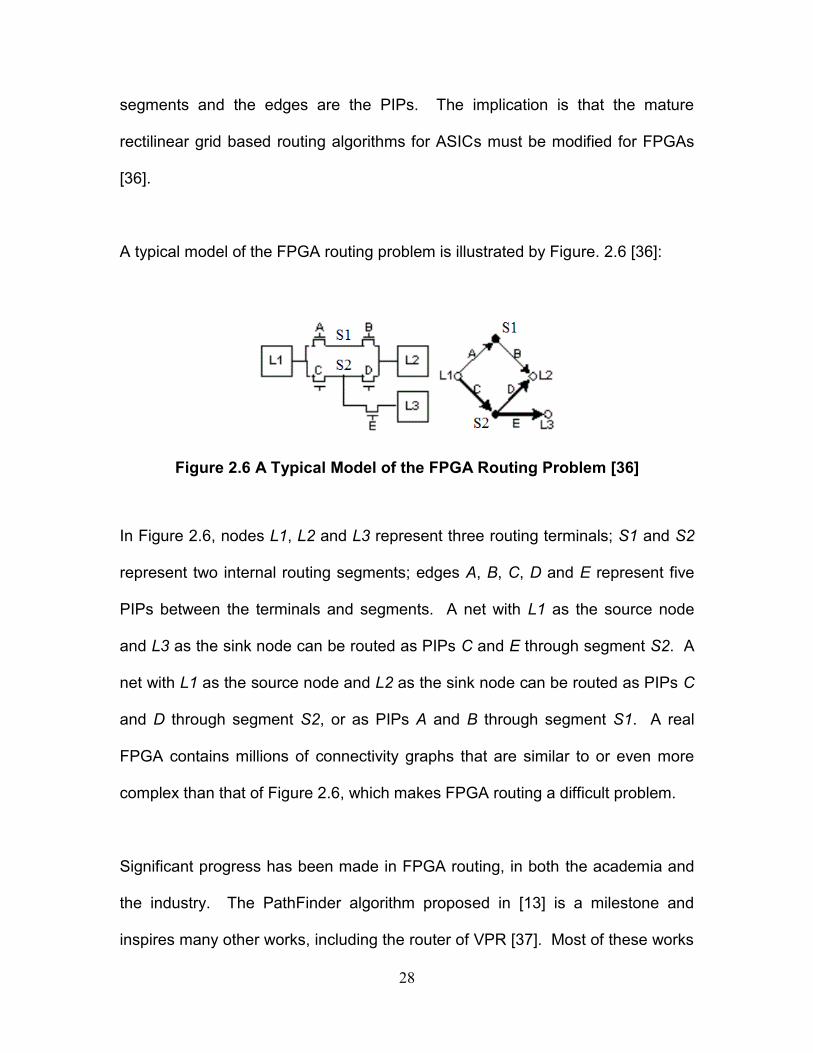
A typical model of the FPGA routing problem is illustrated by Figure. 2.6 [36]:
Figure 2.6 A Typical Model of the FPGA Routing Problem [36]
In Figure 2.6, nodes L1, L2 and L3 represent three routing terminals; S1 and S2
represent two internal routing segments; edges A, B, C, D and E represent five
PIPs between the terminals and segments. A net with L1 as the source node
and L3 as the sink node can be routed as PIPs C and E through segment S2. A
net with L1 as the source node and L2 as the sink node can be routed as PIPs C
and D through segment S2, or as PIPs A and B through segment S1. A real
FPGA contains millions of connectivity graphs that are similar to or even more
complex than that of Figure 2.6, which makes FPGA routing a difficult problem.
Significant progress has been made in FPGA routing, in both the academia and
the industry. The PathFinder algorithm proposed in [13] is a milestone and
inspires many other works, including the router of VPR [37]. Most of these works
Page 44
29
fall into either or both of the following two categories: algorithm enhancement or
architecture exploration [38 ~ 42].
On algorithm side, Maze Router based on Lee Algorithm [43] invented half a
century ago is a candidate. Maze Router is non-iterative without rip-up and re-
route. A net is routed one by one. When the current net is routed, the wires
used are marked as unavailable and the maze is updated accordingly. However,
it is known to be slow. Its routing quality is highly dependent on the order on
which the nets are routed, yet there is no solution to determine an optimal order.
A more popular algorithm for solving the FPGA routing problem is PathFinder.
PathFinder consists of two parts: a detailed router, which routes one net at a time
by finding the shortest path constrained by routing cost; and a global planner5,
which updates the congestion cost for all routing resources and calls the detailed
router to reroute any net with conflicting resources. PathFinder operates by
calling the global planner iteratively. Its details are discussed later in Chapter 3.
The core idea of PathFinder is the Negotiated Congestion based on the equation
below:
( ) (1)
5 In the original paper, the term “global router” is used. The term “global router” originates from
ASIC routing. Instead of detailed fine paths consisting of real wire segments, a global router
generates coarse paths. For modern FPGA devices with a huge routing graph, an actual global
router is desired. Therefore, a different term “global planner” is used here.
Page 45
30
Equation (1) defines the cost of using a routing resource n, where dn denotes the
basic cost (the estimated delay is used in [13]), hn is the history congestion (or
the number of conflicts) of the resource, and sn reflects the congestion (or the
number of conflicts) of the resource in the current iteration. As hn keeps
increasing through iterations, the cost of using the routing resource is increased.
Therefore, this routing resource is less likely to be used and alternative routing
resources that cause less congestion are preferred. As long as routing
congestion exists, the conflicted nets will be ripped-up and re-routed during the
next iteration. Finally, all routing congestions are resolved.
Related work adopts the PathFinder algorithm with different implementations for
the detailed router and with modifications on (1) to boost performance. As a
graph search problem, there are many solutions for implementing the detailed
router. Originally, Breadth First Search (BFS) is applied by [13]. Although it
guarantees to find the optimal path, BFS may have run-time overhead. In the
worst case, the whole routing graph has to be iterated before the solution path is
found. A better solution is the A* search [14]. A* is best-first. Although A* still
has to search the whole solution space in the worst case, it normally searches a
much smaller space than BFS does, with the help of proper heuristics. Typical
modifications on (1) include: applying different interpretations of dn, introducing
new terms, etc. An example set by VPR can be found in [44]. This dissertation
applies a similar approach which is presented later.
Page 46
31
Recently, Boolean Satisfiability (SAT) has been successfully applied to FPGA
routing [40]. However, the SAT-based routing suffers from a high memory
requirement. Another shortcoming is that it either succeeds or fails – it cannot
provide a partial solution, for example, 99% of the nets are routed and optimized
according to certain cost heuristics, while the remaining 1% of the nets can be
routed using different cost heuristics. Therefore, the PathFinder algorithm still
dominates.
On the architecture side, most of the works such as [38 ~ 42] make use of an
FPGA architecture that is simpler than that of the real-world FPGAs (even though
some have a silicon prototype of the proposed architecture). They cannot directly
translate the outcomes of their routers into physical netlists for commercially
available FPGAs such as Xilinx devices. Therefore, they have limited capability
of facilitating FPGA reconfiguration applications. A lot of works make use of a
channel-based routing graph extracted from a simplified FPGA architecture as
illustrated by Figure 2.7 [44]. The logic block pins are directly connected to
vertical and horizontal routing channels. Each routing channel has multiple
tracks, which connect adjacent channels through programmable points in
switching boxes. A similar model with more details is found in [38]. Most prior
work cannot produce routing results that can be directly mapped to a real device;
rather, they are more interested in finding a minimal routing architecture with as
fewer channels and racks as possible where benchmark circuits can be routed.
Although these simplified architectures have gained success, they have a few
Page 47
32
problems, compared to the architectures of the real devices. First of all, real
FPGAs have many more pins than the simplified models. For example, the logic
block of the Xilinx Virtex-5 FPGA has at least 56 input pins and 24 output pins
[45] (clock and reset pins are ignored). Second, wires and segments of real
FPGAs are hard to map to routing channels. The number of tracks per channel
may be too irregular to model. Moreover, there may be bidirectional wires that
make the routing graph partially bidirectional. The upgraded version of VPR [46]
is able to model the modern FPGAs more closely, but still it lacks accurate
routing graphs for real devices and its result may not be directly used for FPGA
reconfiguration.
Figure 2.7 A Simplified FPGA Routing Graph [44]
Traditionally, FPGA reconfiguration is manipulated by the vendor tools – like
Page 48
33
Xilinx ISE (Integrated Software Environment) – which perform the routing.
However, alternative reconfiguration approaches prefer to become independent
of vendor tools and to have a dedicated router. The main reason is that a
dedicated router has the capability of managing routing resources at a fine
granularity and thus the flexibility to only route the nets connecting the
reconfigurable modules. Another advantage is that the router may be open-
source and any user is able to adapt it for any specific case like applications in
the embedded environment. Given the progress made in FPGA routing, it still
remains a challenge to develop a dedicated router for a wide range of
commercially available devices. The router must be versatile to fit as many real
devices as possible, and it must provide routing result in the format of real device
configuration that can be directly applied to facilitate reconfiguration.
Early work on routing Xilinx devices dated back to the late 1990s. [47] develops
a maze router for the XC6200C device. JRoute [48] is a run-time router for the
Virex devices. The major problem is on the algorithm side: these routers do not
leverage a rip-up and re-route scheme like the PathFinder algorithm. As a result,
it is questionable how they can handle complex circuits, such as the big ones in
the MCNC [49] benchmark set. Both [50] and [51] apply the PathFinder
algorithm and they successfully route the MCNC benchmark circuits. [50] targets
the old Xilinx XC4000 devices which are much simpler than the contemporary
devices widely adopted in reconfiguration applications. [51] targets the Xilinx
Virtex-II architecture and makes a few simplifications and assumptions that are
Page 49
34
not valid for the contemporary devices. The major problem of [51] is the viability
for new FPGA devices and the minor problem is the ability to provide routing
results in the format of the real device configuration.
There have been customized routers for various FPGA reconfiguration
applications based on Xilinx devices, such as [33, 52, 53]. These routers apply
device-specific and/or application-specific simplifications. Their routing results, in
the real device format, directly facilitate reconfiguration applications. However,
these routers lack the ability to serve as a general purpose router that is able to
route the benchmark circuits for a wide range of devices. Besides, they lack the
flexibility to be utilized in a different reconfiguration application. TORC [22] and
RapidSmith [23] make great progress in providing the data structure for building
a routing graph based on which a versatile FPGA router can be developed. For
VPR and related works, it is very difficult to develop the architecture description
for real FPGA devices. In contrast, RapidSmith and TORC extract the routing
graph from the XDLRC files which are text reports of commercially available
Xilinx tool. This process is highly automated and it is also feasible to extend to
FPGA devices from other vendors. There have already been works such as [32,
54] which utilize RapidSmith to develop routers; while TORC based approach is
adopted in this dissertation work.
2.5. Fast System Prototyping
As mentioned in Section 1.3, for the conventional FPGA use models, the core
Page 50
35
task is to prototype a digital system on an FPGA device and the main challenge
is to reduce the design compilation time. Traditionally, the FPGA design flow is
very similar to the ASIC design flow [2], which contains the following phases:
Phase 1: Design Entry
Describe the design in a format that can be easily translated into
hardware resources, such as the Hardware Design Language (HDL)
and the schematic.
Phase 2: Synthesis
Analyze the logic of the design. Extract Boolean equations, optimize
them and implement them with generic logic cells.
Phase 3: Technology Mapping
Map the generic logic cells to the primitive gates of a given device.
Phase 4: Placing and Routing
Implement the physical netlist where the occupied primitive gates are
optimally placed and connected.
Phase 5: Configuration bitstream generation
Translate the physical netlist into the bitstream file that configures a
given FPGA device.
Phases 1 ~ 2 are normally called the front-end compilation. The back-end
compilation consists of Phases 3 ~ 4. Phase 5 is different between the FPGA
flow and the ASIC flow. For the ASIC flow, this phase is to manufacture the
design on silicon. To expedite system prototyping, the efficiency of the above
Page 51
36
development flow must be enhanced.
One approach to accelerate FPGA compilation is to improve existing algorithms
or develop new methods for each step in the design flow mentioned above. For
example, High Level Synthesis (HLS) [55] utilizes C/C++ to reduce the design
entry and synthesis time; [56] improves the placement efficiency by applying
clustering and hierarchical Simulated Annealing (SA); routability-driven routing
enhances the run time by sacrificing quality [57], etc
Another approach is to exploit the incremental technique [58] which makes use of
the preserved intermediate compilation data and only compiles design changes.
Early efforts on incremental techniques such as incremental synthesis [59],
incremental technology mapping [60, 61], incremental placing [62, 63], and
incremental routing [48, 64] are effective for improving the performance of a
single stand-alone compilation step. However, it is difficult to merge these works
into a full FPGA compilation flow.
Alternatively, reusing modules becomes promising for reducing the FPGA design
compilation time, which fully makes use of the power of modular design [10] and
of the partial reconfigurability of FPGAs. The modular design methodology
makes it relatively easy to identify design changes into modules. The partial
reconfigurability implies that it is feasible to reuse modules at one step,
manipulate the intermediate compilation data, and merge the manipulation back
Page 52
37
to a full compilation flow.
Module reusing may apply to any compilation step. For design entry, Azido [65]
creates technology-independent designs that are re-targetable and can be
reused across a wide range of FPGA devices. For synthesis, early efforts from
FPGA vendors such as Xilinx’s SmartGuide [66] and Altera’s Incremental
Compilation [67] resynthesize only the portions of the design that have changed
and effectively reuse the unmodified portions. These efforts at the front-end
compilation phase fail to significantly reduce the overall compilation time because
of two reasons. Reason one: the back-end compilation phase normally takes
much more time than the front-end. Reason two: the thumb of rule is that the
later phase at which pre-compiled modules are reused, the more compilation
time is saved; for all the previous compilation phases are skipped and only the
remaining steps are carried out. It is worthy of noting that there is no free lunch:
the decrease in compilation time comes at the cost of degraded performance,
such as area and timing since there are fewer margins for optimizing the design.
The next few paragraphs review the efforts to reuse modules at the back-end
compilation phase in detail.
HMFlow [68], based on RapidSmith, reuses the physical implementation of a
module. A fully placed and routed module is stored as a hard macro in the XDL
format. The module can then be assembled in any design by routing its I/O
interface connections. The FMA proposed here is similar to RapidSmith but has
Page 53
38
the following advantages. Instead of the physical implementation, the
configuration bitstream of a module is reused, and thus more compilation time is
saved. In contrast, HMFlow has to convert the text-based XDL netlist into
physical netilist in the NCD format (which may take as long as tens of minutes for
a huge design) and then to the configuration bitstream. For module connections,
RapidSmith uses a simple non-negotiation based Maze router, but this
dissertation implements a versatile FPGA router using the PathFinder and A*
algorithms.
QFlow [69, 70] is similar to HMFlow. Modules are also pre-compiled as XDL-
based hard-marcos. The difference is that in QFlow, pre-built modules are only
placed but not routed. To assemble the modules with the static design, vendor
tool such as Xilinx par has to be utilized to route the internal nets of the modules
as well as the inter-module connections. Since the pre-compiled module is not
routed, QFlow does not require a clean sandbox with all routing resources
reserved. Instead, any region with enough logic resources that match a pre-built
module is valid. Compared to the FMA, the advantage of QFlow is that routing
by the vendor tool is more likely to have high quality in terms of timing (but timing
requirement is normally relaxed for system prototyping); the disadvantage is that
QFlow normally runs one magnitude slower, due to the fact that it has to route
significantly more nets, i.e. the nets of the modules, and that it has to converted
the physical netilist in the NCD format to the configuration bitstream.
Page 54
39
Ma developed core-based incremental placement algorithms to reduce the FPGA
compilation time [71]. She presented a prototype of FPGA design tool based on
an incremental placement algorithm. It has the feature of exploring a garbage
collection and background refinement mechanism to preserve design fidelity. [81]
mainly focuses on placement with the argument that placement is the most
important back-end compilation phase because of its difficulty and its effects on
the routing performance. It uses JRoute [48] to route a full design and JBits [72]
to generate the configuration bitstream for the design. JRoute and JBits are
Java-based APIs developed by Xillinx, but they have been obsolete for years and
it is impossible to extend them to new FPGA devices.
Hortal and Lockwood [73] propose the idea of Bitstream Intellectual Property
(BIP) cores. The BIP cores are pre-compiled Intellectual Property (IP) modules
that are represented as relocatable partial bitstream. Similar to [73], the pre-
compiled modules for the proposed FMA are also represented as bitstream.
However, [83] makes use of the slot-based reconfiguration. Inter-module
connections must match specific bus macro interfaces with fixed routes. If a
design needs a new module, the full compilation flow needs to be run on the
whole design once more, although other modules in the design may not have
changed. By contrast, the proposed FMA is slotless without fixed-location
sandboxes or fixed-location bus-macros. It is able to locate modules to wherever
there are enough resources and then route the connections. If a module must be
updated, only that module has to be recompiled.
Page 55
40
Last but not least, the Xilinx Hierarchical Design Methodology [74] has become a
breakthrough for incremental compilation. It provides the Partition Flow and the
Preservation Flow, which enable a partition of the design to be reserved and
reused at three different levels: synthesis, placement, and routing. In order to
improve timing, the routing preservation for a partition can be violated. In
contrast, the proposed FMA requires the routing preservation to be kept with no
violation; otherwise, the bitstream level reuse cannot be leveraged. The Xilinx
PR Flow can also be used for fast system prototyping by reusing the partial
configuration bitstream of a module. The proposed FMA serves a different
purpose from the current Xilinx PR Flow. Each module in Xilinx PR is compiled
with respect to a single design framework, i.e. the static design. For a module to
be reused with a different design framework, the whole design must be
recompiled. The proposed FMA can reuse modules for different (but compatible
regarding the interface to modules) static designs. Additionally, Xilinx PR is
intended for the run-time reconfiguration, while the proposed FMA is for off-line
full bitstream assembly. All Xilinx utilities are closed-source and users have to
comply with the required procedure. GoAhead improves Xilinx Modular Design
and PR Flow. The difference from this dissertation is that GoAhead complies
with the vendor’s tools and uses scripts to manipulate them, but this dissertation
follows the C/C++ framework of TORC to develop the FMA technique, which has
as little dependence on vendor tools as possible.
Page 56
41
2.6. Autonomous Adaptive Systems
In modern computing systems, the raw computing power coupled with the
proliferation of computer devices has been growing at an exponential rate for
decades, which has led to unprecedented levels of complexity [75]. To
overcome the problem of complexity, the conception of AAS has been proposed.
An AAS manages its functionality, resources and adaptation without outside
intervention. Consequently, the increasing complexity is absorbed into the
system itself.
Unlike a conventional system that only survives under a certain environment, an
AAS adapts to changes in the environment by modifying its functionality without
external intervention or guidance. To a degree, this mimics living organisms,
which have been autonomously making adaptations to survive in various
environments over a long period of time.
Figure 2.8 A Simplified Diagram of An AAS
A simplified diagram of an AAS is illustrated in Figure 2.8. A typical scenario
Page 57
42
where an AAS would be useful is a system under extreme circumstance (like
deep space, deep underwater, deep within the Earth's crust) that encounters a
fault, a defect, or an unanticipated condition. Humans may not be able to reach
the site physically to service the device, and the remote repair via electronic
signal might be unreliable. While the well-established solution is to increase the
redundancy of the system by applying fault-tolerant techniques, such as Triple
Modular Redundancy (TMR) [76], autonomous systems also provide a promising
solution where the system recovers by self-adaptation [77].
Four key properties of an AAS are introduced here: responsiveness, self-
awareness, intelligence and reconfigurability. The system is responsive to
stimulus caused by changes in the environment, for example, the temperature
fluctuation, the radiation variation, or the protocol alteration. It is self-aware of its
internal resource utilization. It exhibits properties of intelligence (albeit, artificially)
by applying or developing a strategy on how to adapt to the changes. It is
reconfigurable, which means its behavior and functionality can be modified
whenever necessary. Currently, FPGAs are no longer just one part of an
embedded system; they represent the entire platform [77]. Of the four properties
of an AAS, the programmable nature of FPGAs conveniently provides
reconfigurability. Various FPGA IP cores meet the remaining three AAS
properties. For example, I/O peripherals serve as a channel for exchanging
information with the environment and thus provide responsiveness property;
intelligent and self-aware mechanisms can be implemented as programs running
Page 58
43
on microprocessor cores. Therefore, as a reconfigurable embedded System-on-
Chip (SoC) platform, FPGAs are ideal for implementing AASs.
Dynamic partial reconfiguration (PR), mainly adopted on Xilinx FPGAs, is an
enabling technique for autonomous embedded systems. With PR, it is feasible to
change part of an FPGA's functionality at run time by downloading configuration
bits through the Internal Configuration Access Port (ICAP). At the same time, the
remaining part of an FPGA remains functioning normally with no hesitation.
Although the Xilinx PR flow keeps improving, substantial research on extending
the Xilinx PR flow has been done in order to reduce the time and effort required
to successfully use the PR feature. In [11], a slotless partial reconfiguration flow
based on Wires on Demand [31] was presented and research activities on
improving the original PR flow were briefly reviewed. When an AAS is adapting,
it is desirable that other parts of the chip remain working. On the one hand, a
fatal system error might occur if some critical application, such as a
communication unit, ceases to work. On the other hand, extra resources might
be required to store the state of the machine to make the system resume normal
work after being forced to pause during the adaptation. Therefore, the
adaptation process should apply a reconfiguration technique similar to dynamic
PR. In fact, quite a bit of research on autonomous systems use Xilinx FPGAs
[78~81]. Moreover, [82] divides the FPGA reconfiguration based system
adaptation into three types. First, “blind reconfiguration”, i.e. the system blindly
loads pre-built bitstream of the out-of-date modules until the system restores its
Page 59
44
normal operation. Second, “partial reconfiguration”, i.e. the system applies
certain algorithms to determine which pre-built bitstream are desired and loads it
to update the obsolete modules. Third, “run-time reconfiguration”, where there
are no pre-build bistreams and the system instantiates the desired functionality
and generates the corresponding bitstreams for the modules in order to adapt.
“Blind reconfiguration” [82] and “partial reconfiguration” [79, 80] applies a low
level of autonomy since all possible adaptations are pre-determined by the pre-
built bitstream library and it is hardly possible to add new functionality into the
library during run time; while “run-time reconfiguration” [78, 81] applies a high
level of autonomy where any desired adaptation may be configured on the fly.
This work adopts this “run-time reconfiguration”.
Earlier work on autonomous systems focused on how software drives the system
and considered hardware to be static – the system cannot arbitrarily modify its
hardware configuration. Carlisle [83] defined the data management system
functions that integrated all space station subsystems to enable space station
autonomy. Ganek and Corbi [7] announced the dawning of the autonomic
computing era and extended autonomic computing concepts to general IT
systems. Since then, research has been actively carried out on autonomous
systems. The HELI project by Bergerman in the CMU Autonomous Helicopter
Lab [84] developed a software controller that autonomously stabilized a
helicopter's flight. Roman et al. [85] invented the situation awareness
mechanisms that enabled nodes in a wireless sensor network to autonomously
Page 60
45
determine the existence of abnormal events. Research on autonomous systems
that dynamically manipulate their hardware configuration only began in the past
decade [78~81, 86].
One of the early efforts to apply dynamic hardware is the work of [87] by Stitt et
al. It focuses on how to partition an application among software running on a
microprocessor and hardware co-processors implemented in on-chip
configurable logic. Besides proposing a method to do the partition, it develops a
tool set to implement the hardware in the configurable logic during run-time.
Even though this ability to dynamically build hardware is the key in many of the
works on autonomous systems reviewed below, the main motivation of this work
is performance optimization rather than autonomous adaptation. Another
limitation of this work is that unlike [78~81], it does not target a widely adopted
commercially available FPGA device.
Macias and Athanas proposed an autonomous and highly self-reconfigurable
artificial system using the Cell Matrix architecture in [86]. Cell Matrix stipulates
the two key features of biological systems, i.e., autonomy and locality of control.
This architecture is futuristic, and is premised on the scalability to billions of cells.
Upegui and Sanchez in [78] presented an approach to convert concepts of
artificial intelligence from software modeling into real evolvable hardware. The
authors built Random Boolean Networks (RBN) using off-the-shelf reconfigurable
hardware – the Xilinx Virtex-II Pro (XUP) FPGA board [88]. A RBN cell is
Page 61
46
designed as a hard macro whose configuration bits are manipulated through PR
to stimulate the RBN evolution rules. Macias and Athanas [86] and Upegui and
Sanchez [78] used a bottom-up approach to build autonomous systems with the
main focus on the function of low-level cells as hard macros. The authors of
[79~81] applied a mixed-level approach: the system autonomy and adaptation
behaviors are abstracted at a high level as circuit functionalities while low-level
effort is required for implementing them in hardware. The same general
approach is applied by this dissertation.
Steiner in [81] generated a working prototype of an Autonomous Computing
System on the Xilinx XUP board. It not only used PR for system adaptation, but
also generated configuration bits autonomously. Famhy et al. in [89] claimed that
Steiner’s work provided a foundation for building adaptive systems. [89] mainly
tackled adaptation challenges by proposing the software architecture. This
software framework absorbed away the low-level hardware details. However, the
AAS developed in [81] as well as in this dissertation tends to achieve a high level
of autonomy with the ability to implement the adaptation in hardware. It might be
over-optimistic to assume that based on Steiner’s work, it is trivial to implement a
hardware framework for building an AAS on newer FPGA devices. From a
practical perspective, various challenges need to be overcome to implement an
AAS on different platforms, such as adapting to different hardware IPs and
developing different embedded utilities.
Page 62
47
Steiner in [81] also proposed a roadmap for building an autonomous system and
defined the levels of autonomy. To implement the lower levels of autonomy, a
vendor tool is sufficient. For example, French et al. in [80] developed an AAS
dedicated to signal processing with the Xilinx PR flow. However, it does not have
the ability to autonomously implement new functionality and update the hardware
configuration accordingly. For the higher levels of autonomy, the system must
have the ability to manage the logic and routing resources at a fine granularity to
instantiate any new functionality, as demonstrated by [81].
Page 63
48
Chapter 3
A Versatile FPGA Router
Section 2.4 discusses the preliminaries, background and incentives of the
proposed FPGA router. Here is a brief summary. Like many established FPGA
routers, the router here utilizes the well adopted algorithms for FPGA routing, i.e.
PathFinder and A* Search. Unlike the routers with a simplified or artificial routing
architecture, the router targets real devices with the help of TORC, and produces
results directly applicable to FPGA reconfiguration applications. Compared to
early work on routing real devices, the router here is more versatile without any
application-specific or architecture-specific assumptions. Being versatile, the
router is able to route benchmark circuits on a wide range of commercially
available devices.
This chapter focuses on the implementation details of the router, the experiment
results as well as the demonstration applications. Section 3.1 presents the
routing graph based on the data structure of TORC. Section 3.2 shows the
overall flowchart. Section 3.3 discusses the implementation of an actual Global
Page 64
49
Router. Section 3.4 presents the Detailed Router (or Signal Router6) based on
the A* algorithm. Section 3.5 explains the core idea of PathFinder algorithm, i.e.
iteratively rip-up and re-route, through the Global Planner. Section 3.6 lists the
results of applying the router to route 18 MCNC benchmark circuits on five
selected Xilinx devices. Section 3.7 demonstrates how to use the router for the
reconfiguration application of creating routing-free sandboxes. Section 3.8 first
summarizes the topic of this chapter regarding the big picture, and then draws
conclusions about the router and highlights the potential future work.
3.1. Routing Graph
The problem of accurately modeling an FPGA routing graph is solved by TORC
[22]. TORC has a Device Database with exhaustive knowledge on the logic and
wiring of many real devices. TORC builds the database through parsing and
compressing non-proprietary XDLRC files, similar to the work of the Alterative
Wire Database (ADB) [90]. TORC has an API that grabs the logic and wiring
information of a given device from the Device Database and stores the
information in a C++ object. This object contains the architecture description of
the give FPGA device, from which an accurate routing graph is built.
The preliminaries of the FPGA architecture based on TORC’s data structure are:
A device is divided into two-dimensional grids of tiles.
6
Detailed Router and Signal Router are equivalent terms and this chapter uses them
exchangeable.
Page 65
50
A tile contains a set of wires, which are electrical nodes.
A segment is a collection of abutting wires on adjacent tiles.
A PIP is the programmable connections between two wires.
A segment is a node and a PIP is an edge in the routing graph by applying the
graph theory terms.
For a given Xilinx FPGA device, all tiles, wires, segments and PIPs are fully
described in its XDLRC file, from which the routing graph is built. An example of
a simplified version of such a routing graph is illustrated by Figure 3.1. The
graph is different from the widely used channel-based model, and it accurately
models a real device. Another feature of this routing graph is being architecture
independent. No matter how big or how small a device is and no matter how
simple or how complex it is, its XDLRC file is processed in the same way by
TORC and the similar data structure is used to build the routing graph.
Figure 3.1 A Simplified Example of the Routing Graph Extracted from XDLRC
Currently, this method only applies to Xilinx FPGAs, but the idea is extendable to
Page 66
51
devices from other FPGA manufacturers if they made device data available in a
similar format to that of XDLRC.
With the help of TORC, the router is able to produce results as routing PIPs in
the XDL format. An example of PIP is:
pip INT_X62Y84 LOGIC_OUTS3 -> NW2BEG2, # comment
“pip” is the keyword denoting that the remaining of this line defines a PIP.
“INT_X62Y84” is the name of the tile where this PIP locates. “LOGIC_OUTS3” is
the name of the source wire of the PIP and “NW2BEG2” is the name of the sink
wire. “->” indicates the type of the PIPs is unidirectional and buffered. Most of
the PIPs are of this type. “,” means the end of the PIP definition. “#” is for
adding comments.
Moreover, other types of PIPs include: “==” for “bidirectional and unbuffered”, “=>”
for bidirectional and buffered in one direction”, and “=-” for “bidirectional and
buffered in both directions”. These types of PIPs are relatively scarce. Being
bidirectional, they offer routing flexibility to a large degree; but they also make the
routing graph more complicated, because the graph is no longer acyclic
3.2. Overall Flowchart
The overall operation of the proposed router is illustrated in Figure 3.2. There
are four steps:
Step I: Initialization: The design is imported in the XDL format. The
Page 67
52
corresponding device database is loaded and the routing graph is built. If a wire
or a PIP has already been used in the imported design, the corresponding node
or edge is marked as used on the routing graph and becomes unavailable for the
router. In this way, incremental routing is feasible.
Step II: Global Router: All nets in the design are coarsely analyzed. The
global analysis determines whether the actual global routing should be run.
Step III: Initial Routing: All unrouted nets are routed greedily without
considering any congestion, i.e. is set to 0 and is set to 1. and are
initially used in equation (1) and defined in Section 2.4.
Step IV: Rip-up and Reroute: The routing resource conflict map is updated
to renew and . If any net uses a wire that has , the net is unrouted
and then routed again. The above process is repeated iteratively until no routing
conflict exists.
The Global Planner part of the PathFinder algorithm consists of the Initial Routing
step and the Rip-up and Re-route step. To route a net, it calls the Detailed
Router.
Note that no particular processing on the net ordering is performed. Whatever
ordering resulted from converting the design into XDL format is accepted. [35]
Page 68
53
suggests that rip-up and re-route technique normally eases the problem of net
ordering, but it also admits that there are cases where smart planning on net
ordering helps. Intelligent net ordering may be a branch of future work.
Figure 3.2 The Overall Flowchart of the Proposed Router
Page 69
54
3.3. Global Router
The function of a Global Router is to generate a coarse route for a net. The
coarse route is then obeyed by the Detailed Router. As mentioned earlier, a
device is presented by two-dimensional grids of tiles. These are very fine grids.
For example, the Virtex-5 LX110T device has a grid of 177 164 tiles. The
Global Router divides the device into much coarser grids, say 8 6 bins.
An example of a Global Router is illustrated in Figure 3.3. The device is divided
into 12 bins, from grid (0, 0) to (3, 2). Each bin consists of some invisible grids
which represents tiles. Net 1 gets the coarse route: (0, 0) → (1, 0) → (2, 0) → (3,
0) → (3, 1); Net 2 gets the route: (1, 1) → (2, 1) → (2, 2) → (3, 2). How a Global
Router runs is described in detail later.
Figure 3.3 A Global Router Example
The reason a Global Router is needed is because without global routing, the A*
based Signal Router may become trapped in a congested region. Multiple nets
compete for one specific routing resource in this region and no alternatives are
Page 70
55
available, which leads to unresolvable routing conflicts. In this case, a Global
Router may noticeably reduce the routing conflicts that the Pathfinder algorithm
has to resolve and the runtime of Pathfinder may decrease. However, as shown
later (the last paragraph of Section 3.4), the course-grid route generated by
Global Router constrains the Signal Router and slows it. Therefore, Global
Router may or may not help reduce the overall run time and it should only be run
if the Global Analysis phase determines that it is necessary.
It is difficult to quantify the Global Analysis. The original PathFinder algorithm [3]
does not require a Global Router to generate coarse nets. How a Global Router
improves the performance of the original PathFinder is not a well-studied
problem7. This dissertation applies the following policies learned from practice:
If initially there is an existing design and the router is to add some new
nets, calculate the density of the used routing resources of each bin. If
any bin is highly crowded (say more than 80% of all the segments
within the bin are used), the Global Router has to be run.
If initially there is no existing design, or if the existing design does not
have a region where the routing resources are highly crowded, Initial
Routing is run without the Global Router. If the results show that the
majority of the nets (say more than 80% of all the nets) have conflicting
wires, the Global Router has to be run and then continue with Initial
7 The original PathFinder does not have a real Global Router. Xilinx par uses a Global Router to
facilitate later detailed routing, but how it works is not published. VPR also has a Global Router,
but that is for its channel and rack based routing graph.
Page 71
56
Routing again. Otherwise, there is no need to run the Global Router
and the next step is Rip-up and Reroute.
For the experiments performed in this dissertation, the following
lessons are learned. For the application of creating a routing-free
sandbox, the Global Router must run. The reason is that all routing
resources in the sandbox region are treated as occupied which is an
extreme example of a highly crowded region. For routing benchmark
circuits, the Global Router is not needed, because generally the
signals to route spread throughout a device and there is no highly
crowded region. Stitching modules for the FMA is somewhere
between the above two examples. In theory, it is possible that the
starting point and the ending point of an inter-module connection is in a
congested area, so that Global Routing is required; however, in
practice, it is difficult to produce a case to demonstrate this8.
Admittedly, the above policies are more or less tentative. Deterministic and
quantitative heuristic analysis on whether Global Router has to be run should be
developed. However, no satisfying solution is available now. It should be a
candidate for future work. Currently, it is sufficient to conclude that the Global
Router is essential and successful for the routing-free sandbox creation
application, as demonstrated later in Section 3.7.
8 The modules are compiled by Xilinx tools with as little constraint as possible, and the tools are
intelligent enough to avoid putting I/O pins in a very congested area.
Page 72
57
The Global Router starts by calling the Kruskal’s algorithm [91] to generate a
minimal spanning tree for each unrouted net. The tree covers the bins where a
net’s source pin and sink pins are. A coarse net for each minimal spanning tree
is generated through a rip-up and re-route process similar to Pathfinder. During
one iteration, the cost map for all bins is firstly updated. Then, for each net, its
coarse route generated by the previous iteration is cleared and a new coarse
route is generated using the Dijkstra’s algorithm [91].
3.4. Detailed Router
The Detailed Router routes a single source wire to one or more sink wires. It
makes use of the A* algorithm to search the XDLRC based routing graph for
minimal cost paths. How the Detailed Router operates is illustrated in Figure 3.4.
The Detailed Router runs with a priority queue of route nodes, where a node is a
directed arc on the routing graph. Initially, if the net is partially routed, the arcs
already been used by the net are inserted into the queue; otherwise, a dummy
arc representing the source wire of the net is inserted.
A route node has a source wire and a sink wire. If the current route node’s sink
wire is the same as the destination sink wire, routing is done. Otherwise, a new
route node is created for each arc going out of the current route node’s sink wire
or any abutting wire that belongs to the same segment. The new route node is
set as a child of the current node, so that once the destination sink wire is
Page 73
58
reached, it is easy to trace back to the root route node to complete the routing
path.
Figure 3.4 The Flowchart of the Detailed Router
Before a new route node is inserted into the routing queue, its cost is evaluated.
A* is a best-first search and its cost function must have good heuristics to guide
the search. The evaluation of A* is given by the following equation:
Page 74
59
(2)
is the path cost of using a node N. is the estimated optimal path cost from
the current node N to the goal node G. It is heuristic because the actual path
from N to G does not exist until the search reaches G. It has to be admissible,
meaning that "the cost of N to G is never overestimated". is the optimal path
cost from the start node S to N. Since the path is already built, this cost should
be accurate. The requirement for is that it “never decreases along the path”.
If is always 0 (or equivalently a constant), the special case of A* becomes the
"greedy" search, which makes the locally optima search at each searching stage
and does not in geneneral produce the optimal solution. In normal cases,
counts for the established path cost from the starting node to the current
expanding node, not simply the local cost of the estimation from the expanded
nodes to the desitnation node. In other words, represents the effort towrd
finding the global optima.
If is always 0, this special case of A* becomes the "uniform cost" search,
which only considers the global optima of the expanded path cost from the
starting node to the current node. The problem here is without being constrained
by , the search tends to be blind about where the destination is. As a result,
the search may take too much time or it may even fail to converge to the
destination. More or less, helps to achive a fast convergence in the way
similar to the “greedy” search.
Page 75
60
It is feasible to apply the A* with BFS. If BFS reaches the destination at a
certain depth, it may finds more than one path leading back to the root node and
it selects the most optimal one. However, BFS needs to fully search the tree
from the root node to all the leaves at the current depth. In contrast, A* normally
only has to search a portion of such a tree, and hence is faster and more
memory efficient than BFS. Such benefits come at a cost – A* may not find all
candidate paths as BFS does so that it may miss the most optimal path.
Because of the limitation that the accurate timing information is not available and
the fact that the original PathFinder does not apply the A* search, equation (1)
must be modified here. By considering the routing graph built from TORC and
the explanation of equation (2), the cost of using a route node n is defined by the
following equation:
α β (3)
Equation (3) is explained as the following:
The first term is the “path heuristic”, which is the product of “distance
heuristic” and “delay heuristic”. “distance heuristic” reflects
the distance between the tile where the current route node n is and the
tile where the destination sink wire is. Its purpose is to make sure that
the A* search finally reaches the destination. “delay heuristic” helps
to improve the timing of the final route. A thumb of rule for a route from
a source wire to a sink wire is: the fewer PIPs that the route consists of,
Page 76
61
the smaller the delay of the route is. The reasoning is that fewer PIPs
lead to fewer resistors and capacitors. Therefore, “delay heuristic”
of a route node is simply set as its depth in the searching tree.
Ideally, timing information like wire delay model from FPGA
manufacturers should be used. However, such knowledge is not
published and thus not applicable for determining “delay heuristic”.
(4)
How to calculate is discussed in detail later. As the
searching tree expands, n gets closer to the sink wire, and hence
decreases. between n and the sink wire is never
overestimated. reflects the delay cost of using n to get to the
sink wire. It is never overestimated as well since the actual depth to
get to the sink wire cannot be smaller than the depth of n. Therefore,
the product of and is admissible and serves as the A*
heuristic cost in equation (2).
The second term is the “congestion heuristic” which helps to resolve
the routing conflicts. The term is the product of and . is the
sum of the historic conflict count of all routing nodes from the source
wire to current node n. Similarly, is the sum of the current conflict
count from the source wire to n. As the searching tree expands,
more nodes are inserted into the path from the source wire to current
node n, so and never decreases along the path. The product of
Page 77
62
and serves as the A* optimal path cost in equation (2).
(5)
With two heuristics, the routing becomes a multiple objective
optimization problem. Both terms have distinct value domains so they
may not be directly summed up. Rather, they should be normalized
and then weighted. The normalization is the single-objective function
used widely in Computer-Automated Design (CAD):
(6)
Apply (6) to (4) and (5), the normalized “path heuristic” and “congestion
heuristic” used in (3) are calculated by the following equations
respectively:
(7)
(8)
and in equation (3) are weight coefficients for normalized distance
and conflict heuristics respectively. In this work is set to 0.1 and is
set to 0.9. These are tentative values that are found to produce
satisfying results through experiments.
Page 78
63
Figure 3.5 How to Calculate the Distance Heuristic
How to calculate the distance heuristic is illustrated in Figure 3.5. If the Global
Router is not run, the distance heuristic is simply the Manhattan Distance
between the tile where the current route node resides and the tile where the sink
wire is. If the Global Router is run, the calculation is more complicated. If the
current route node is at a grid that is out of the coarse route, the distance is set
as infinite and such route node is never inserted into the routing queue. If the
current route node is within the coarse route, locate the turning grid where the
coarse route changes direction. The distance heuristic is the summation of the
following two terms:
: it is the Manhattan Distance between the tile where the
current route node is and the center tile of the turning grid.
: if there is no further direction change from the turning
grid to the sink node, it is the Manhattan Distance between the center
tile of the turning grid and the tile where the sink wire is; if there is
Page 79
64
further direction change, it is set to the length of the coarse route from
the turning grid to the sink grid.
In case that the Global Router is run, the distance heuristic is strictly larger than
the distance heuristic in case that the Global Router is not run, according to the
Triangle Inequality Theorem. In other words, by following the constraint of the
coarse route generated by the Global Router, the resulting route has a longer
path, compared to the route without the Global Router constraints. Generally, it
takes more time to construct a longer route. This is one reason why the Global
Router constraints may slow the Signal Router, as mentioned previously. In
other words, the A* heuristic of the Signal Router has to learn to keep on the
coarse route generated by the Global Router constraints.
3.5. Global Planner
The global planner keeps a hash table T that maps a routing resource n to its
conflict count at the current iteration and its overall conflict count through all
the iterations. It first calls the detailed router to route any unrouted nets (initially,
all nets are unrouted). Then it iterates all the nets to update :
If the current net uses a routing resource n that does not exist in T – it
means n has not used by any routing through all the iterations up to now,
create a new entry in T for n with and ;
Page 80
65
If the current net uses a routing resource n that exists in T – it means n
has been already been used, increment by 1
The Global Planner performs rip-up and reroute iteratively through the following
three steps:
Step 1: rip-up
It iterates all the nets one by one. If the current net uses a routing
resource n with equal to or greater than 2 – it means n is used by more
than one net, i.e. a routing conflict occurs, mark the current net as
conflicted;
Step 2: unroute
It then iterates all nets again to unroute any net marked as conflicted.
When a net is unrouted, decrement by 1 for all routing resources which
the net occupies. A trick here is for a multiple-sink wire, it is not
completely unrouted. Instead, only the paths containing a conflicting
routing node with are undone. This idea is similar to "maintaining
wave-front" in VPR, which may help reduce the overall routing time.
Step 3: reoute
After a net is unroted, the detailed router route it again. For any resources
n used by this routing, increment by 1 if n exisits in T; otherwise, create
a new entry in T for n with and .
When all nets are iterated, is updated:
Page 81
66
Iterate all entries in T, for each routing resource n, its is updated by
adding to it.
The above process is repeated for as many iterations as possible, until there is
no net to unroute in Step 2.
3.6. Experiments on Benchmark Circuits
The MCNC benchmark circuits are widely used by the research community for
testing the performance of routers. The main interest here is on the router only,
so the Xilinx tools are used to map and place the circuits. Since these circuits
are only available in the BLIF [92] format, which is not supported by Xilinx tools,
the BLIF tool [93] is used to convert the circuits into the VHDL format. Then the
Xilinx utilities are called to re-synthesize, map and place the circuits. These post-
placed circuits are converted to the XDL format and then used by the proposed
router.
The benchmark circuits are routed for five different devices: XC3S100E,
XC3S1600E, XC4VFX12, XC4VLX200, and XC5VLX110T (XC3S100E is the
smallest Spartan-3E device and XC3S1600E is the largest in the Spartan-3E
family. XC4VFX12 is the smallest Virtex-4 device and XC4VLX200 is the largest
in the Virtex-4 family. XC5VLX110T is a widely used Virtex-5 device in the
research community.) Table 3.1 reports the run time of each routing as well as
the run time of timing-driven VPR and Riverside On-Chip Router (ROCR) from
Page 82
67
[38]. The results of VPR and ROCR are only used for rough reference rather
than for competitive comparison. The main reason is that these two routers use
a much simpler routing model that is far from a real device. Moreover, due to the
re-synthesizing, mapping and placing mentioned above, the nets to route in each
circuit are not 100% the same between [38] and the work here. Another factor is
that the results are not obtained from the same computers.
TABLE 3.1 THE RUNTIME OF ROUTING THE MCNC BENCHMARK CIRCUITS ON
DIFFERENT DEVICES (IN SECONDS)
Router VPR ROCR XDLRC Router
device [38] [38]
XC3S100
E
XC3S160
0E
XC4VFX1
2
XC4VLX2
00
XC5VLX11
0T
BE
NC
HM
AR
K
alu4 8.3 0.6 0.35 0.50 0.44 1.60 0.97
apex2 12.4 4.3 6.38 3.34 3.58 10.23 7.63
apex4 7.8 0.6 0.44 0.62 0.51 0.87 0.37
bigkey 13.5 1.3 1.78 2.38 3.26 3.58 4.10
des 12.8 1.0 1.40 1.62 1.71 2.43 2.08
diffeq 5.8 0.4 6.32 5.50 4.59 13.31 9.33
dsip 10.4 0.9 1.12 1.20 1.23 2.22 3.44
E64 1.0 0.1 0.12 0.17 0.14 0.17 0.26
elliptic 33.7 7.8 N/A 18.4 19.72 21.73 34.11
Ex5p 6.3 0.3 0.05 0.05 0.05 0.06 0.05
frisc 35.1 13.8 N/A 34.2 30.60 28.15 49.05
misex 6.8 0.4 0.30 0.37 0.32 0.59 0.59
s1423 0.5 0.1 0.86 0.97 0.70 1.13 1.95
s298 11.6 0.7 4.85 6.69 3.73 6.84 4.33
s38417 49.9 8.7 N/A 35.4 33.74 38.68 35.79
s38584.1 36.0 8.8 N/A 17.1 11.22 11.25 24.25
seq 11.4 2.2 0.68 1.31 0.56 0.81 2.05
tseng 3.1 0.2 3.72 3.52 3.35 6.28 6.31
Each test case, i.e. a specific benchmark circuit on a specific device, is run 10
times. The average of 10 runs is reported in the table. The “N/A” for column
XC3S100E means the circuit is too large to be implemented on that device.
What is not shown in the table is that the results of the proposed router are in
Page 83
68
Xilinx’s XDL format and can be directly converted to FPGA configuration.
Therefore, the routing results can be directly applied in FPGA reconfiguration
applications. For example, they can be instantly converted into the configuration
binaries to program a target FPGA device.
Here are some interpretations about the fiures shown in the table. First, by using
a binary metric of success or failure, the italic figure in one cell explicitly proves
that the proposed router is able to route the benchmark circuit for the given row
on the target device for the given column. The few “N/A”s on the column of
XC3S100E does not imply that the router should fail but only indicates it is not
big enough for the corresponding benchmark circuit. Second, similar to the VPR
and ROCR routers, whose results are quoted from [38] and listed in column 2
and 3, respectively, the router succeeds in routing all the 18 MCNC benchmark
circuits. And the run time (0.05~6.38 / 0.05~35.4 / 0.05~33.74 / 0.06~38.68 /
0.05 ~ 49.05 seconds for the device XC3S100E / XC3S1600E / XC4VFX12 /
XC4VLX200 / XC5VLX110T, respectively) is comparable to that of VPR
(0.5~49.9 seconds) and ROCR’s (0.1~13.8 seconds) – neither dominantly
smaller nor dominantly larger. Third, unlike the VPR and ROCR routers which
model a hypothetical and simplified FPGA architecture [38], the router here
targets the commercially available devices. With the help of TORC, the router
here is able to route all the selected five devices as in Table 3.1. These devices
represent a wide range of Xilinx FPGAs which are frequently used in applications
leveraging FPGA reconfiguration.
Page 84
69
The proposed router is only tested on Xilinx devices because currently only the
Xilinx devices have XDLRC that describes its architecture and resource graph.
For a similar reason, most research work on FPGA reconfiguration applications
focus on the Xilinx devices. However, the proposed router should apply to
FPGAs from other vendors if they release the device architecture description in a
similar format which is compatible to XDLRC.
3.7. Demonstration Applications
The router aims to facilitate FPGA reconfiguration, and two FPGA reconfiguration
applications are developed to demonstrate this claim. The first application, i.e.
stitching modules for the slotless reconfiguration, is presented in Chapter 4 as an
essential component of the FMA technique. This section presents the details of
the second application, i.e. creating a routing-free sandbox.
The flow of creating a routing-free sandbox has four steps:
Step I. Read in the design source files, such as the HDL files;
Step II. Analyze the sandbox parameters and create the implementation
constraint file;
Step III. Synthesis, map, and place the design using the constraint file;
Step IV. Route the full design and reroute the nets that resides in the sandbox.
Step I~III are the same as in the OpenPR flow [34], where the same Xilinx utilities
Page 85
70
are used to implement the design. For OpenPR, all the nets in the design are
routed through fpga_edline in Step VI; for the flow here, after the design is routed
by par, any net that goes through the sandbox is unrouted and then rerouted with
the proposed router. That’s why the flow here runs much faster than OpenPR for
creating a routing-free sandbox. It is worthy of noting that creating routing-free
sandboxes is only part of OpenPR, and it also provides other features like
generating partial configuration bitstream for any module to be put in the sandbox.
However, OpenPR does not work on huge designs, like the Convey Computer
[94].
(a) (b) (c)
Figure 3.6 The Routing-free Sandbox Creation for A Video Filter Design
(a) Original Netlist, (b) Sandbox Created by OpenPR, and (c) Sandbox
Created by the Proposed Router
Figure 3.6 (a) ~ (c) show the original netlist of a 24-bit VGA video filter, the
sandbox created by OpenPR, and by the proposed router, respectively, on the
Xilinx XC5VLX110T device. Both sandboxes are routing-free. The major
Page 86
71
difference is the run time. The OpenPR flow takes around 4 minutes and 30
seconds and the flow here takes around 2 minutes 46 seconds - about 60% of
the OpenPR’s run time.
Regarding the timing performance of the designs shown in Figure 3.6, ideally the
original design in Figure 3.6 (a) should have the best performance, since it is
routed by Xilinx par in an iterative way similar to PathFinder without extra
constraints. Figure 3.6 (b) should have worse performance since not only it has
extra routing constraints, i.e. a routing-free region, but also it is routed by Xilinx
fpga_edline in a non-iterative way. For the similar reason, Figure 3.6 (c) also
should have worse performance than Figure 3.6 (a) – it has extra routing
constraints and the offending net is rerouted by the proposed router. It is not
easy to determine whether Figure 3.6 (b) beats Figure 3.6 (c) in timing. Figure
3.6 (b) uses fpga_edline which is not iterative but as a vendor tool, it is able to
optimize the absolute value of routing delay using the built-in wire delay model.
Figure 3.6 (c) uses the proposed router which is iterative but since the wire delay
model is not known, it is only able to relatively optimize the routing delay by using
fewer PIPs. The actual result is: the maximum frequency of Figure 3.6 (a) is 179
MHz. The maximum frequency of Figure 3.6 (b) is 210 MHz. Since the target
frequency is only 50 MHz and the design is relatively simple, the surprise that
Figure 3.6 (b) outperforms Figure 3.6 (a) is an acceptable exception. The
maximum frequency of Figure 3.6 (c) is also 179 MHz, which implies the nets
rerouted to bypass the sandbox are not on the critical paths.
Page 87
72
(a) (b)
Figure 3.7 The Routing-free Sandbox Creation for Bigger Designs
(a) medium size design – tseng, on XC5VLX110T, (b) huge size design –
Convey, on XC5VLX330 device
The results of using the proposed router to create a routing-free sandbox for
larger designs are shown in Figure 3.7. It is interesting to point out that there are
two ways to implement the sandbox of Figure 3.7 (a). The first method does not
use a Global Router and the run time is 19.38 seconds. The second method
uses an actual Global Router, which takes around 0.04 seconds to generate
coarse nets. The overall run time is only 8.66 seconds, which is smaller than half
of the run time without the Global Router. The explanation is that without the
Global Router, the PathFinder Signal Router based on A* has to learn that the
routing wires in the sandbox are forbidden during run time. It may hit into the
sandbox many times before it eventually learns to go around it. With the Global
Router, coarse routes outside the sandbox are planned before the PathFinder
Page 88
73
router is run. Then the Signal Router only has to follow the guidance generated
by the Global Router. Moreover, without the Global Router, the routing result
contains around 14.1k PIPs; with the Global Router, the figure goes down to
13.0k, which implies a higher routing quality.
3.8. Summary, Conclusion and Future Work
To summarize, this chapter focuses on the topic of developing a versatile FPGA
router. It combines the desirable features of the routers from existing research
on both routing architecture side and algorithm side. The chapter starts by
addressing the issue of building the accurate routing graph for real FPGA
devices. It then reveals the implementation details of the proposed router’s
major components which adopt the well-accepted algorithms. The experiment
results and demonstration applications prove why the router is “versatile” - it is
able to route the benchmark circuits over a wide range of commercially available
devices and to directly facilitate applications based on FPGA reconfiguration.
Consequently, the router is an upgrade as compared to many existing FPGA
routers. Moreover, it is essentially the “routing” manipulation which plays an
important role in the “fast reconfiguration” and the “self-reconfiguration”
discussed later.
In conclusion, this chapter presents an FPGA router based on the PathFinder
and A* algorithms. By utilizing the routing graph built upon TORC Device
Database with the information extracted from XDLRC files, this router not only
Page 89
74
targets a wide range of real devices, but also produces results that can be
directly turned into FPGA configuration. Therefore, the router is a candidate for
FPGA reconfiguration applications where a dedicated router is needed. The
performance of the router was evaluated by running it on the MCNC benchmark
circuits for five different devices. The typical usage in FPGA reconfiguration was
demonstrated by two applications, namely the FMA and the routing-free sandbox
creation.
For future work, the A* evaluation function should be modified such that the path
cost models delay information more accurately. Non-constant coefficients should
be used. For example, the congestion coefficient should be increasing through
iterations. Therefore, for later iterations, the penalty of using a conflict wire
increases, the probability of using the wire decreases, and the time for resolving
all conflicts shrinks. Also, an individual net should be assigned a priority value
according to whether it is on the critical paths. A net with higher priority value
tends to have a bigger path coefficient and a smaller congestion coefficient,
which means the net has the higher priority to optimize timing and to use conflict
wires. Another enhancement is to find a detailed solution for the problem of how
to improve PathFinder with a Global Router. Moreover, it might be interesting to
figure out a way to convert the XDLRC routing model into the simplified routing
channel and rack model. In this way, it is feasible to take advantage of existing
algorithms for that simplified routing model.
Page 90
75
Chapter 4
Fast Module Assembly
Here is a brief recall of the motivation and background of the FMA. The FMA is
part of the Turbo Flow (TFlow) [15]. TFlow aims to significantly accelerate the
FPGA back-end compilation for modular designs and to enhance the productivity
of the FPGA design development. To achieve software-like compilation time, the
FMA not only reuses the configuration bitstream of pre-built modules, but also
stitches the loaded modules at the bitstream level. With the help of the FPGA
router from Chapter 3, the FMA applies the idea of slotless reconfiguration,
where modules are pre-built flexibly without excessive constraints.
This chapter is organized as follows. Section 4.1 talks about the prerequisites for
running the FMA, i.e. the briefs of all the preparation steps in TFlow before the
design assembly stage. Section 4.2 presents how to load and relocate a pre-
compiled module. Section 4.3 presents how to stitch the loaded modules.
Section 4.4 discusses the optional debug scheme to verify the correctness of the
module assembly. Section 4.5 shows experiment results as well as comparison
against the traditional ISE flow and the recently developed QFlow. Section 4.6
starts with a brief summary of the general topic of the chapter. It then draws
Page 91
76
conclusions and makes suggestions for future work.
4.1. Prerequisites
Figure 4.1 [15] illustrates the process of how TFlow runs. There are mainly two
phases, i.e. the module creation phase, which generates the component library
with pre-built modules, and the design assembly phase, which generates the
configuration bitstream for a full design by assembling the modules. Currently,
TFlow only applies to Xilinx FPGAs, especially the Virtex-5 family.
The module creation phase looks very similar to the normal process of how an
FPGA designer implements a module. The designer describes a module using
any design entry method like HDL or schematic. He/she synthesizes the design
and generates its Electronic Design Interchange Format (EDIF) netlist using
Xilinx XST. Then he/she uses Xilinx’s Partition Flow [74] to place and route the
design. It is desired to repeat placing and routing several times with different
shaping constraints. As a result, each module has a profile with implementations
of different shapes and different applications are free to pick up the best-fit shape.
There are no constraints for later assembly, because the FMA does not apply
any pre-built channel or specific communication protocol for stitching the
modules. The only constraint is to use Xilinx’s Partition Flow, which has a
consistent naming convention for the anchor points, i.e. a module’s input and
output pins, between the post-synthesis EDIF netlist and the physical netlist.
TFlow uses the APIs from TORC to import the EDIF netlist of a module and the
Page 92
77
physical netlist of each implementation of that module. Then TFlow extracts key
attributes, such as the shape, anchor points, resource usage, etc., and store
these attributes in a meta-data file of the Extensible Markup Language (XML)
format. To register a module in the library is to create a profile consisting of XML
meta-data files and configuration bitstream files for each shape.
Figure 4.1 How TFlow Runs [15]
The second phase is the design assembly phase. The designer specifies what
modules to use and how to connect them. He/she stores the information in a
meta-data XML file. TFlow then processes the XML file, fetches the module
profile from the library, and starts the module assembly. The first step is to
assign the modules optimal locations and update the meta-data XML file. TFlow
Page 93
78
applies a placing scheme similar to the placer in QFlow [69]. The second step is
to relocate the configuration bitstream of the modules and this is when the FMA
begins to take charge. All previous steps of the module creation phase and the
design assembly phase discussed above are prerequisites. The FMA continues
with the final step of the module assembly, i.e. stitching the modules into the final
bitstream file for the full design.
4.2. Module Relocating
A Xilinx FPGA is configured by downloading a configuration bitstream file into its
configuration memory. A bitstream file consists of frames of binaries
representing specific logic and routing configurations. A frame is the smallest
addressable segment in a bitstream file. A frame has an address with fixed
length and a certain amount of raw configuration bits
Figure 4.2 How to Divide a 32-bit Frame Address into Six Fields [95]
For the Virtex-5 FPGAs, the frame address is a 32-bit word and has six fields [95].
Page 94
79
Figure 4.2 shows how to divide a 32-bit frame address9. The details about these
six fields are:
Bits 31 ~ 24 are reserved and unused.
Bits 23 ~ 21 represents the Block Type. Normally, one block consists
of one or more columns of tiles. There are two block types which are
programmable by the users. One type is BRAM contents, with the
block type code 001. The other type is Interconnections and Non-
BRAM Blocks with block type code 000. Non-BRAM Blocks include
CLBs, DSP blocks, and Input/Output Blocks (IOBs).
Bit 20 is the Top/Bottom bit. 0 represents the top half of a device and
1 represents the bottom half.
Figure 4.3 The Top/Botoom Bit and the Raw Address in Xilinx FPGA10 [95]
9 For other device family, the frame address normally still has six fields but the definition of each
field may be different.
10 This applies not only to the Virtex-5 FPGAs but also to most other Xilinx FPGAs.
Page 95
80
Bits 19 ~ 15 represent the Row Address. Vertically, a device is divided
into several major rows, or Horizontal Clock (HCLK) rows. Each row is
20-tile in height. Figure 4.3 shows how to decide top/bottom bit and
major row address.
Bits 14~7 represent the Major Address. Each major row has multiple
columns of different block types. Each column of tiles has a column
address, determined by its column coordinate and its block type. The
column address is the same as the Major Address. Figure 4.4 shows
clearly how to assign the Major Address within a row, where the light-
gray sequence is for Non-BRAM blocks and the dark-gray sequence is
for BRAM blocks.
Figure 4.4 The Assignment of Major Addresses in a Major Row [95]
Bits 6~0 determine the Minor Address. Given the Block Type, the
Top/Bottom Bit, the Row Address and the Column Address, a specific
column is hit. One column contains a certain number of frames and
the Minor Address is used to access the desired frame. The exact
Page 96
81
number of frames inside a specific column depends on the column’s
block type, as Table 4.1 shows
TABLE 4.1 THE EXACT NUMBER OF FRAMES PER COLUMN
Block Type Number of Frames
CLB and CLB Interconnections 36
DSP and DSP Interconnections 28
IOB and IOB Interconnections 54
BRAM Interconnections 30
BRAM Contents 128
Figure 4.5 How the Bitstream Level Module Relocation Works
The right side of Figure 4.5 also explains the above six fields with the snapshot of
the XC5VLX20T device’s layout. There are two major rows on the top half with
the Row Addresses 0 and 1; there is one major row on the bottom half with the
Row Address 0. There are three columns of the block type 001 (BRAM content),
Page 97
82
so their Major Addresses are 0, 1, and 2; all other columns are of the block type
000 (including CLBs, DSP blocks, and IOBs) and their Major Addresses are 0, 1,
2, 3, …. , 30. For the group of frames marked by the red ellipse, they belong to
column 3 of Major Row 0 at the bottom half. They are either CLB tiles or CLB
Interconnection tiles, so there are 36 frames in the group, with the Minor Address
from 0 to 35.
The basic idea of the configuration bitstream relocation is illustrated in Figure 4.5.
Raw bits of all configuration frames are stored in the bitstream file. The location
of a configuration frame determines a Frame Address Register (FAR) value, from
which the frame index within all configuration frames is calculated. This frame
index maps to a file address, which is used to grab the raw bits of the
corresponding frame from the bitstream file. To relocate the configuration bits to
a new location, the new FAR value is generated for this location and then
converted to the new frame index. The new frame index hits a new file address.
Relocating one frame is accomplished by moving the raw bits at the old file
address to the new file address in the bitstream file. Take relocating one frame
in the green ellipse for example. Its location on the device determines that its
FAR value is 0x11808E. This FAR value means that the frame is the #16308
frame in among all configuration frames. The Frame Index of 16308 maps to the
file address of 0x103456 in the module bitstream file. The raw bits of the frame
to relocate reside at this address. Grab them and put them in a buffer. Suppose
the target location is in the red ellipse. This location determines the target FAR
Page 98
83
value of 0x300C9. This new FAR value is the #21321 frame in the base design
bitstream file. This new Frame Index of 21321 maps to the file address of
0x20654 in the base design bitstream file. To relocate the frame is to copy the
buffered raw bits of the frame to this new file address in the base design
bitstream file. To relocate a module is to repeat the above frame relocation
process for all the frames in the module. Effectively, all the logic and routing
configuration of the module are moved, and this is effectively the manipulation
“relocating” defined in Section 1.3.
The raw bits of a Virtex-5 configuration frame consist of 41 32-bit words. Its 32-
bit address maps to 20 tiles on the same major row. 40 out of the 41 words
encode the configuration of each tile’s logic elements and routing resources (2
words per tile) and the middle word has miscellaneous information including the
clock network settings. Currently, a module is relocated on the base of offsets as
major rows by moving the raw bits of a frame from the old location on a major
row to the new location on another major row for all frames. Therefore, there is
no need to further parse and modify the raw bits. However, in order to relocate
with a higher resolution, i.e. not on the base of major row but on the base of tile
row, raw bits must be modified. This will be discussed later in the future work
section.
It is worthy of noting that this relocation scheme only works if the target region is
a completely empty sandbox where no logic or routing resource is occupied. The
Page 99
84
reason is explained in Section 2.3 which discusses the challenge of creating a
routing-free sandbox. The demonstration application in Section 3.7 provides one
way to create such a sandbox. Another approach is to force Xilinx par to follow
routing constraints by creating a dummy net which occupies all possible routing
resources for entering and exiting a region. The second approach is able to
maintain the maximum clock frequency of the static design as much as possible,
because the primary goal of par is to optimize timing. However, in theory, this
approach still does not guarantee that the routing constraints are 100% followed;
par allows violation in order to enhance timing.
4.3. Module Stitching
After placer places the modules, the updated meta-data XML file contains the
following information for stitching the modules: the inter-module connections and
the routing constraints. Each inter-module connection has one source pin and
one or multiple sink pins. The source and sink pins are in the XDL format as
“Site_Name. Pin_Name”, such as:
Source: SLICE_X24Y40.D
Sink: SLICE_X18Y74.B3 SLICE_X21Y73.C5 SLICE_X22Y72.D5
The routing constraints are the routing resources used by the relocated modules.
They are also in the XDL format as PIPs, such as:
PIP INT_X21Y34 CTRL2 -> CTRL_B2 ,
An API calls the FPGA router from Chapter 3 and makes use of the above
information to route the inter-module connections through the following steps:
Page 100
85
Step I. Load the static design by using TORC XDL importing utility. By
importing an existing design, the router automatically knows what routing
resources are used by the static design.
Step II. Load the routing constraints from the meta-data file and flag
the PIPs as used. The router then avoids using these PIPs.
Step III. For each inter-module connection, create an unrouted net in
the loaded design. Create an array with these unrouted nets.
Step IV. Call the router to route the array of unrouted nets from Step III.
The output of the router is the routing PIPs of the routed inter-module
connections in the XDL format.
Step V. Translate the routing PIPs from the XDL format into
configuration bits. Set up the configuration bits in the bitstream file of the
full design with relocated modules, which is generated in Section 4.2.
The two key steps are Step IV and Step V. They represent the manipulation
routing defined in Section 1.3. For Step IV, Chapter 3 has discussed the router
in detail. Step V is the low-level manipulation that ensures the assembly speed.
This step relies on a “routing configuration bits database”. Each PIP needs a set
of configuration bits to activate. Recall the explanation on the definition of a
routing PIP in Section 3.1. Each routing PIP has a “tile name”, which represents
its the location. Section 4.2 has mentioned that the location of a tile maps to a
FAR value representing the address of a configuration frame with 41-word raw
bits. In fact, the (X, Y) coordinate of a tile determines a “word offset” D_offset
Page 101
86
which means that among the 41 words, the configuration of all routing resources
at this tile is in word #D_offset. To hit a specific bit, two more offsets are needed,
“byte offset” B_offset and “bit offset” b_offset, because one word has four bytes
and one byte has eight bits. How to calculate B_offset and b_offset? There is a
one-to-many mapping between the pair of a PIP’s source wire and sink wire and
a few pairs of byte offset and bit offset. The “routing configuration bits database”
stores such information. A PIP has a few entries in the database and each entry
has values including the source wire name, the sink wire name, the byte offset
and the bit offset. The database is on a MySQL server and Step V accesses the
database through a MySQL client to query the configuration bits for a given PIP.
Without the capability of low-level manipulation, Step V has to generate the XDL
netlist for the full design. Such an assembly scheme is almost the same as that
from RapidSmith, i.e. through reusing the XDL netlists of fully placed and routed
modules. This scheme needs two more actions: to convert the XDL netlist into
the physical netlist and to generate the configuration bitstream file based on the
physical netlist. The second action alone inevitably requires more time than
directly setting a portion of the bits in a bitstream file – tens of seconds vs. a few
seconds. Worse still, the first action may take a few hours for a big design like
the Convey. In this case, the only difference from RapidSmith may be that the
router here potentially has better performance since the original RapidSmith only
has a basic non-iterative maze router.
Page 102
87
Currently, the configuration bit level module stitching approach only applies to the
Virtex-4 and Virtex-5 devices. It is not applicable to other devices, since the
relationship between the routing PIPs and the corresponding configuration bits is
unknown.
4.4. Debugging
Manipulating FPGA configuration at the configuration bit level is so delicate that a
debugging scheme is necessary. The approach is to perform the module
relocation and stitching at the XDL level instead of at the configuration bit level.
It is exactly the same assembly scheme without the low-level manipulation as
discussed in the last section. Because this XDL-based assembly scheme is
much less error-prone, the resulting bitstream file for the full design is treated as
golden. This golden bitstream file is compared to the assembled bitstream file
generated through the configuration bit level manipulation. If there are zero
different configuration frames between them, the assembled bitstream is error-
free. Otherwise, the assembled bitstream has errors and they can be debugged
using the contents of the different frames. Possible errors include: configuration
bits of a module are relocated to a wrong place, or the router makes a bad route,
etc.
One debugging trick is to isolate the configuration bits modified by module
relocating from those modified by module stitching. To achieve this, instead of
directly comparing the golden and the assembled bitstreams files of the full
Page 103
88
design, compare the bitstream files for the intermediate design after module
relocating first. If there are no different frames, it means the configuration bit
level module relocation has no error. Then compare the bitstreams files of the
full design after module stitching. If there are different frames, it must come from
the PIPs of inter-module connections generated during module stitching.
4.5. Demonstration and Experiment Results
Figure 4.6 shows a demonstration of applying the FMA to the GNU radio
development [96] on the XC5VLX110T device.
(a) (b) (c)
Figure 4.6 Applying the FMA for a GNU Radio System Development
(a) the static design, (b) relocating the modules, (c) stitching the modules
The static part of the system is a basement design for receiving and transmitting
radio signals. As Figure 4.6 (a) shows, there is a big sandbox for holding
modules that perform signal processing. In Figure 4.6 (b), seven modules are
Page 104
89
loaded into the sandbox, including a Low Pass Filter (LPF), the ZigBee radio core,
FIFOs, etc. The configuration bits of each module are read from the pre-built
bistream file and then relocated into the bistream file of the static design. The
router from Chapter 3 is called to make the connections to assemble the modules.
The resulting nets are marked in red in Figure. 3.4 (c). Note that it is feasible to
do the assembly by using Xilinx par with the “-k” option in the re-entrant route
mode. However, that takes around 40 seconds. In contrast, the proposed FMA
finishes module stitching in around 0.5 seconds. This is 80 times speedup.
Moreover, it takes Xilinx utility bitgen more than 30 seconds to generate the
configuration bitstream for the full design. With the FMA, the total assembly time
including module relocating and module stitching is around 1 second.
Since the FMA is the final steps of TFlow, it would be more meaningful to show
the results of comparing TFlow with other compilation flows. Two other flows in
consideration are: the traditional Xilinx ISE flow and QFlow. The traditional ISE
flow is the normal compilation flow which does not reuse any pre-built modules.
QFlow reuses the physical netlist of modules that are pre-placed but not routed.
TFlow reuses the configuration bitstream of pre-built modules that are fully
placed and routed.
A test case is designed as follows. Each flow starts with a post-synthesis EDIF
netlist of a given design for a target FPGA device. The ISE flow first packs and
maps the EDIF netlist onto the target device. It then performs placing and
Page 105
90
routing using its utility par and implements the physical netlist of the design.
Finally, it converts the physical netllist into configuration bitstream using the utility
bitgen. QFlow uses the EDIF netlist as guidance to pick up the desired static
design and the pre-built modules. It then runs the module placer to assign
optimal locations for each module. After that, it merges the physical netlists of
the static design (fully placed and routed) and the relocated modules (placed but
not routed). To stitch the modules into the final physical netlist, it calls par to
route the intra-module nets and the inter-module connections. It also relies on
bitgen to generate the final configuration bitstream file. TFlow uses the EDIF
netlist for the same purpose as QFlow does. It also runs a similar module placer
as QFlow does, but the later steps are different from QFlow. TFlow merges the
configuration bitstream of the static design and the pre-built modules into a full
bitstream file. To stitch the modules, it runs the dedicated router from Chapter 3
to build the inter-module connections. It converts the routing results into
configuration binaries and directly set them in the full bitsream file. TFlow does
not need to run bitgen. Essentially, each flow performs the back-end compilation
starting with a post-synthesis netlist of a design and ending with the configuration
bitstream of the full design.
For each flow, there are four test cases. The first test case is to implement an
Edge Filter in the video filter design as Figure 3.6 shows. The second test case
is the same as the first one except that it replaces the Edge Filter with a
Gaussian Filter. The third test case is similar to the radio design shown in Figure
Page 106
91
4.6. The static design is still a basement for receiving and transmitting radio
signals, and the dynamic modules represent the core components of a ZigBee
Radio. The fourth case is the huge Convey design as Figure 3.7 (b) shows with
a Vector Adder to implement in the sandbox. While the ISE flow directly
implements the full design from scratch, QFlow and TFlow reuses pre-built static
design and modules and implement the full design through module assembly.
Table 4.2 compares the resource utilization of the different flows. Table 4.3
summarizes the performance of each flow on different test cases in terms of the
overall compilation time.
TABLE 4.2 THE RESOURCE UTILIZATION COMPARISON (THE FULL DESIGN)
Test Case
SLICE DSP BRAM
ISE
Flow
QFlow /
TFlow
ISE
Flow
QFlow /
TFlow
ISE
Flow
QFlow /
TFlow
Edge Filter 2865 2838 14 14 0 0
Gaussian
Filter 2062 2068 18 18 0 0
ZigBee Radio 1648 2028 10 10 8 9
Vector Adder 22444 11443 0 0 53 60
Table 4.2 shows that QFlow and TFlow have the same resource utilization. This
is because QFlow and TFlow compile a module in a similar way. The difference
is QFlow only places but does not route the module and reuses its physical
netlist, while TFlow fully places and routes the module and reuses its
configuration bitstream. Compared with the ISE flow, there is no resource
utilization overhead. This proves the claim that with the FMA, modules are pre-
Page 107
92
compiled in a flexible way without excessive constraints – just as many
constraints as the normal ISE flow may use; no more, no less. Therefore, TFlow
should have the similar resource utilization as compared to the ISE flow. Test
Case One to Three supports this statement. Test Case Four, however, is an
exception where the resource utilization of the TFlow implementation is almost
50% of the resource utilization of the ISE flow implementation. The reason is
that in Case Four, the Convey design is very large and takes up almost half of
the total SLICEs available on the target device. For a dense design like this,
TFlow’s effort in shaping the modules and the static design to some degree tends
to compact the logic and hence reduce the resource utilization. In contrast, for a
dense design, ISE tends to use as much logic resource as possible. In this way,
most logic elements have a low fan-out count and they have limited load, which
helps to improve the timing performance
TABLE 4.3 DESIGN COMPILATION (BACK-END) TIME COMPARISON
Test Case Compilation time (seconds) TFlow Speedup QFlow Speedup
ISE Flow QFlow TFlow Over ISE Flow Over QFlow Over ISE Flow
Edge Filter 184.6 170.8 21.6 8.5x 7.9x 1.1x
Gaussian Filter 159.8 156.7 17.8 9.0x 8.8x 1.0x
ZigBee Radio 236.2 157.7 23.8 9.9x 6.6x 1.5x
Vector Adder 3891.7 805.1 98.7 39.4x 8.2x 4.8X
The compilation time of ISE flow in Table 4.3 not only serves as a base for
calculating the QFlow/TFlow speedup, it also reflects the complexity of the
design to a certain degree. For test Case 1 and Case Two, the filter designs as
Page 108
93
well as the static design are not very complicated. Therefore, QFlow fails to
achieve a noticeable speedup against the ISE flow, and the speedup is only 1.1x
and 1.0x respectively. In contrast, the compilation time of TFlow is significantly
less than that of the ISE flow, and the speedup is 8.5x and 9.0x respectively. For
Case Three, the ZigBee radio design as well as the static design is slightly more
complex than the designs of the previous test cases. As a result, the speedup of
TFlow over the ISE flow increases moderately to 9.9x and the speedup of flow
over the ISE flow increases noticeably to 1.5x. The Convey design of test Case
Four is very dense and very complex. Therefore, the speedup of TFlow over the
ISE flow and that of QFlow over the ISE flow take a sharp jump to 39.4x and 4.8x
respectively.
The conclusion of the above observation is that TFlow has a significant speedup
over the ISE flow for accelerating the back-end compilation and the speedup
increases as the design complexity grows. However, with an extremely
complicated design, this increase may slow down, it may become negative, or
there will be no speedup at all. For such a design, it may not be possible to
create routing-free sandboxes for modules. In this case, the FMA technique is
not applicable because it is impossible to relocate the modules. Hence TFlow
fails at module relocating and the speedup is 0. Even if routing-free sandboxes
are available, the router may have difficulty in routing the inter-module
connections. Admittedly, the router from Chapter 3 is not as powerful as par.
Particularly, there is a trick called “pin swapping” in par. Suppose a net’s sink is
Page 109
94
the 3rd pin of a LUT. When par reaches this LUT, it may select its 2nd pin as the
net’s sink. In this way, par does need to take time to trace back its routing tree to
search for an actual path that leads to the original sink pin. However, since now
a different pin is used, the configuration of this LUT needs to be modified. Such
a trick does not apply to the FMA, because the modules are pre-built and their
configuration binaries are fixed. Therefore, the router may take very long time to
route the inter-module connections so that the overall TFlow run time exceeds
the ISE flow’s run time; or the router may simply take forever and hence TFlow
fails at module stitching and the speedup is 0. In contrast, QFlow has much
more chance to survive in case of an extremely complicated design, because it
does not require routing-free sandboxes and it uses par to do the routing.
The compilation time in Table 4.3 does not consider the module compilation for
building the component library in TFflow. The time spent on building the module
might be negligible in TFlow for two reasons. Ideally the Module Creation Phase
is a one-time operation and it is finished offline. The normal on-the-fly operation
is the Design Assembly Phase and usually this operation is sufficient for
compiling a target design. In case that the design needs a new module or an
existing module needs updating, the overhead of compiling a module using Xilinx
tools may not affect the overall TFlow run time. This is because the proposed
FMA as well as the placer does not need Xilinx tools, meaning that the whole
Design Assembly Phase can run in parallel with the Module Creation Phase.
Page 110
95
4.6. Summary, Conclusion and Future Work
In summary, this chapter presents an FMA technique for “fast configuration”.
The inspiration is the software compilation through linking pre-compiled libraries
as executable, which utilizes the reconfigurability and flexibility of software. This
technique consists of two steps: relocating pre-compiled modules and stitching
the modules with the versatile router from Chapter 3. Both steps exploit the low-
level manipulation of FPGA configuration to ensure speed and flexibility. After
discussing the implementation details of these two steps, this chapter
demonstrates an application of how the FMA works for fast developing a radio
system. Following the demonstration, the chapter shows experiment results of
comparing different compilation flows. These results prove the following
statement: the FMA has the potential to be an enabler for an alternative FPGA
compilation flow that dramatically reduces the design compilation time.
The major conclusion is that the proposed FMA is an instant module assembly
technique with flexibility. Compared to running par in the re-entrant route mode
to stitching modules, building inter-module connections with a dedicated FPGA
router is much faster. Another factor for significantly saving compilation time is
the low-level manipulation on configuration binaries, which eliminates the need
for generating physical netlist and converting that netlist into configuration
bitstream. The flexibility comes from the slotless reconfiguration idea which to a
large degree decouples the dependencies between different pre-built modules as
well as the dependencies between the modules and the static designs. With the
Page 111
96
help of FMA, TFlow is able to achieve 8 ~ 39 times speedup as compared to the
traditional ISE flow on designs with various complexities.
As mentioned earlier, relocation with a higher resolution is feasible. This
relocation is one possibility for future work. It is more complex and it has to
manipulate the raw bits of a frame. Generally speaking, the raw bits of the
configuration frame at the old location should be split into two parts and merged
with the raw bits of two adjacent frames at the new location. Moreover, the
proposed FMA may be extended to newer devices, like the Virtex-6 or Zynq
FPGAs, which may encourage the adoption of TFlow as a productivity tool in
both the academia and the industry.
Page 112
97
Chapter 5
Autonomous Adaptive Systems
An autonomous adaptive system is a system that operates independently and
enhances its own behavior and functionality beyond its initial design. In short, an
AAS is a system with the capability of autonomous self-reconfiguration. On the
one hand, FPGA’s run-time partial reconfiguration facilitates to implement an
AAS with the ability to dynamically manipulate its own hardware configuration.
The rest of an AAS should keep functioning while a part of it is undergoing
modification for adaptation. On the other hand, the self-reconfiguration idea from
an AAS helps to ease the difficulty of recompiling a complex FPGA design for
reconfiguration. AAS absorbs much of the computing complexity into itself so
that there is no need to recompile the system externally.
The organization of this chapter is as follows. Section 5.1 describes a framework
for building an AAS. Section 5.2 and 5.3 describe the hardware and software
implementation of a proof-of-concept AAS, respectively. Section 5.4 presents a
demonstration of an AAS with a universal UART transmitter. Section 5.5
analyzes the performance of the embedded tool set designed for an AAS.
Conclusions and potential future work are in Section 5.6, following a brief
Page 113
98
summary of the whole chapter..
5.1. A Framework for Building an AAS
Figure 5.1 shows a diagram that represents the proposed framework of hardware
and software for implementing an AAS.
Figure 5.1 A Framework for Building an AAS
The static requirements of this framework are simple and straightforward. A
configurable fabric like an FPGA is needed so that the system is able to change
its own hardware functionality via run-time partial reconfiguration without being
shut down. Adequate memory is necessary to hold a library of adaptation
strategy and support adaptation applications. The memory also contains a
model of the AAS system itself that contains the logic and routing resource usage
Page 114
99
map. A microprocessor, such as the PowerPC, is needed to manage the
hardware resources and the software utilities. A proper I/O interface is required
through which the system accepts stimulus and feeds back a response. These
requirements are easily met by almost every deployed Xilinx FPGA system,
including the development boards [88, 96].
An AAS built with this framework does not require more resources than a typical
system implemented with FPGAs - most systems consist of an FPGA, memory
and I/O devices anyway. Moreover, the autonomy and adaptation come at an
affordable cost. If the AAS works in a normal environment, its microprocessor
and applications for adaptation can be in the standby mode for most of the time.
Access to the processor may be very light, leaving the processor free to perform
other embedded duties or simply do nothing at all. Only in the unexpected
situations, where self-adaptation is required, should the AAS work in full power.
There are additional costs that could possibly be diminished, yet they greatly aid
the system development. An operating system such as Linux is used to manage
hardware resources and software applications. Embedded Electronic Design
Automation (EDA) utilities like an EDIF netlist parser, mapper, placer, router and
configuration bits manipulator are needed to manipulate hardware at a fine
granularity and instantiate reconfiguration through the ICAP. A suitable cross-
compile tool and/or Java Virtual Machine (JVM) are required for
building/executing these utilities. These runtime requirements, especially the
Page 115
100
task of developing the EDA tools, are the main challenge that this chapter
addresses. However, such effort should be nonrecurring. Most aspects of the
developed tools are able to abstract away the physical details of the underlying
FPGA device, making portability an important development criterion.
5.2. System Implementation – Hardware
The hardware platform for the proposed proof-of-concept AAS is the Xilinx
ML410 board [97]. The board has a Xilinx Virtex-4 XC4VFX60 FPGA containing
two PowerPC 405 hard-core processors and two ICAPs. The board has many
peripheral components connected to the FPGA, such as a DDR2 DIMM memory
slot, two RS-232 serial ports, and a tri-mode Ethernet MAC/PHY. It meets all the
requirements and is an ideal platform for developing a prototyping AAS.
With the Xilinx Embedded Development Kit (EDK), it is fairly easy to build an
embedded system using the Base System Builder (BSB). For a proof-of-concept
AAS demonstration, the system should be as simple as possible. The detailed
hardware structure of the "Adaptive UART Transmitter" demonstration is
illustrated in Figure 5.2.
The demonstration system is built with EDK 10.1 BSB and contains the following
components: one PowerPC microprocessor, one DDR2 memory controller, one
ICAP interface, and I/O devices such as GPIO, the UART and the Ethernet MAC.
All components are IP cores provided by Xilinx, except "uart_0", which is a
Page 116
101
customized simple UART transmitter with 8 data bits, no parity check and no
handshaking. "uart_0" contains a counter that determines the transmission
BAUD rate. The BAUD rate counter is the dynamic module for autonomous
adaptation. The whole system without this counter is referred to as the static
system. The slot-based reconfiguration is applied here for simplicity and the
static system communicates with the counter through bus macros. The details
about the operation of the proof-of-concept demonstration will be presented later
in Section 5.4. It should be noted that this process does not use the Xilinx PR
flow, though they share a few terminologies.
Figure 5.2 Hardware Components of the Demonstration AAS
Page 117
102
A 512M DDR2 memory chip is not shown in Figure 5.2, but it is a required
peripheral to support the embedded software.
It is relatively easy to apply the hardware implementation discussed here to
another AAS for different applications. The basic idea is to design a module
where adaptation is supposed to occur and replace the “uart_0” module with it.
5.3. System Implementation – Software
As mentioned earlier, runtime requirements of the adaptation utilities are the
primary challenge in the proposed framework. The effort within the software
domain is explained here. At first sight, much of the software framework appears
familiar – an operating system, the front-end and back-end compilation tools to
translate a digital design into physical implementation, and the utility to
instantiate the design onto an FPGA. Similar utilities are well established for
desktops or workstations, but they are relatively less mature for the embedded
environment, where the proposed AAS is supposed to operate. Therefore, the
main focus of this paper is to ensure the following feature: the feasibility of the
proposed utilities in an embedded environment. Note that for the sake of being
proof-of-concept, limited effort has been made to pursue high performance for
these utilities. Compared to well-studied algorithms from the literatures, simple
and straightforward strategies are preferred with little consideration regarding the
complexity of the problem.
Page 118
103
5.3.1. Operating System
Linux, due to its high portability, has been successfully used in the embedded
systems based on microprocessors including PowerPC, ARM and MIPS for a
long time [98]. Moreover, many commonly available I/O device drivers map the
device to a character stream in the file system, so reading from and writing to the
I/O device becomes a file operation. Therefore, Linux is the chosen OS here.
Brigham Young University's Linux on an FPGA project serves as a good guide on
configuring and installing a Linux kernel 2.4 onto XUP boards [99]. After the
release of Kernel 2.6.28, the Xilinx Open Source Wiki community [100] has
published the "Device Tree Generator", which makes porting Linux onto the
Xilinx FPGA boards much easier. With this tool, a hardware configuration file is
generated for a system built by BSB, and it is then used to generate a Linux
image for this specific system [101], which contains basic drivers for almost all of
the Xilinx IP cores, including the ICAP. Details of this porting process are
omitted here, and those who interested in this are referred to [102].
A cross-compile tool is required to build executable binaries on the PowerPC - for
the kernel image and the embedded EDA utilities. Embedded Linux
Development Kit (ELDK) [103] is used here.
5.3.2. Pre-processor
Page 119
104
To prepare for operating the EDA utilities, a program called the pre-processor, is
run off-line to analyze the static design. It extracts key information that is used
later online by the embedded EDA tools: the position of the input and output bus
macros, the dimension constraints (where the PR region is on the device), the
resource usage constraints (what logic and routing resources are initially
occupied and must not be reused), and the clock tree configuration. Also, the
bitstream file for the static system generated by the Xilinx tools is patched so that
all columns of a clock tree within the PR region are turned on11. Moreover, it
generates a partial bitstream file of clean_bits for the PR region that clears the
configuration of the region so that no logic and routing resource are used.
5.3.3. EDIF parser
The AAS framework translates an abstract description of the new adaptation
behavior into the actual FPGA configuration with available logic and routing
resources. The AAS is expected to associate events (a detected fault, a new
interface, etc.) to a digital circuit or a set of digital circuits. It is expected to
interpret the abstract descriptions of these circuits and translate them into
available FPGA resources. The AAS maintains a library of potentially deployable
circuits for adaptation.
Ideally, the library should use HDL descriptor, such as Verilog or VHDL, or even
more abstracted language, such as SystemVerilog and SystemC, to describe
11
This approach is more stable than setting the clock bits using the configuration bits manipulator
during run time through ICAP.
Page 120
105
these anticipated behaviors. This dissertation work assumes that an AAS does
not need to perform synthesis. Therefore, an adaptation description is a
technology-specific post-synthesis netlist in a widely accepted format, such as
the Electronic Design Interchange Format (EDIF). The reason is that an FPGA
synthesizer is difficult to develop: the problem of converting design entry files into
Boolean equations and optimizing these equations is NP-hard; and how to map
the optimized equations on to FPGA-specific logic cells is proprietary.
An EDIF netlist needs to be parsed before being passed to the placer and router.
The EDIF parser created by Brigham Young University [104] serves this role
5.3.4. Mapper and placer
After parsing, all information about a netlist, including what cells are instantiated,
what ports each cell has, what nets exist, how the cells are connected, and what
properties each cell has, etc., is extracted and stored in an internal data structure
in the memory. The embedded mapper and placer are also written in Java so
that they can directly use the EDIF parser's internal data.
The mapper and placer begin by building a circuit graph, where each node is a
cell and each edge is a net connecting two cells. Since the EDIF netlist is
assumed to be synthesized targeting a specific technology, i.e. a Xilinx FPGA,
each cell is an instance of basic elements within the Xilinx Unified Library [105].
Currently, only a subset of the library is supported: all kinds of LUTs, all kinds of
Page 121
106
FDs, MUXF5, MUXCY and XORCY. This is nonetheless sufficient for simple
demonstrating designs.
The mapper works by merging two connected nodes into a new super-node if the
super-node fits into the smallest logic unit of the FPGA, or SLICE for the Xilinx
Virtex-4 FPGA. For example, a LUT and FD are merged into a LUT-FD pair; two
LUTs, one MUXCY and one XORCY are merged into a MUXCY-XORCY pair, etc.
Also, any carry chain formed by MUXCY-XORCY pairs is detected. More
formally, the mapper performs the task of "slice packing”.
After the mapper packs cells into super-nodes and maps them to real
components on an FPGA slice, the placer assigns a location to each super-node.
First, input and output buffer nodes are placed, since they have a fixed location
at input and output bus macros. Second, special groups of super-nodes, for
example, carry chains, are placed, since they normally consume multiple slices
and are less flexible to place. Then, for the remaining nodes, a simple greedy
strategy is applied: the super-nodes are sorted accordingly to their weight, which
reflects their fan-in and fan-out and is a metric of congestion. The greedy
strategy begins by placing the super-node with the highest weight and places its
fan-out super-nodes around it. These super-nodes become the first cluster.
Then, the placer chooses the node with the highest weight among the remaining
unplaced super-nodes, places it at some distance away from the first cluster, and
places its fan-out super-nodes around it. These super-nodes become the
Page 122
107
second cluster. Eventually all nodes are clustered and placed in this way. The
flowchart of the above process is illustrated in Figure 5.3. The outcome of the
placer is an intermediate text file containing routing paths for the router and logic
configuration directives in the XDL format.
Figure 5.3 The Flowchart of the Greedy Placer
The placer has two additional features. To ensure the routability of the
placement, it is desired that no locations become too crowded. Therefore, a local
weight parameter that adds the weight of all nodes placed around a location is
Page 123
108
checked. If the local weight exceeds a threshold, the remaining super-nodes of a
cluster are placed at the current location but moved to a new location. The other
feature is that the placer takes resource usage constraints from the preprocessor
and gains knowledge about which locations are forbidden for placement. With
this feature, existing circuitry can be avoided, and it is feasible to isolate and
replace defects in the device by adding more entries in the constraint list.
The performance of this placer is not optimal, yet the goal here is not to develop
an expert placer; rather, any placement that can be routed by the router is
deemed to be an as proof-of-concept one. Moreover, there is no dedicated
floating-point unit in the Virtex-4 PowerPC. Established placing algorithms, such
as Simulated Annealing [5] would need to rely on software emulation, and would
require too much memory and time – at lease more than what is necessary for a
proof-of-concept system.
5.3.5. Router The intermediate file generated by the placer provides the input for the router.
The router’s task is to route each path and generate the corresponding PIPs.
The router makes use of a connectivity database derived from XDLRC, which
contains most connection pathways within the Virtex-4 FPGA. Ideally, the router
from Chapter 3 should be used here. Even though that router is potentially able
to run in the embedded environment, a lightweight version of it is actually
developed here. Figure 5.4 lists the pseudo code of this lightweight router.
Page 124
109
Figure 5.4 The Pseudo Code of the Router
Table 5.1 summarizes the difference between the versatile router from Chapter 3
and the lightweight router for the proof-of-concept AAS. The versatile router is
able to route a wide range of commercially available Xilinx devices, but the
lightweight router only targets the Virtex-4 family. For each Virtex-4 device, the
versatile router stores an absolute connectivity database based on TORC. There
are 17 databases in total and the overall size is bigger than 40MB, even after
compression. During run time, the versatile router loads one database for the
target device and builds the corresponding routing graph. Obviously, the
database of the smallest device, i.e. Virtex-4 FX12, needs the least time to load,
which is about 309 milliseconds; the loading time for the largest device, i.e.
Page 125
110
Virtex-4 LX200, is around 2161 milliseconds; and on average the loading time is
860 milliseconds. However, there are many redundancies among these
databases. Different devices have different sizes, but their layouts generally
consist of a huge two dimensional array of tiles. Each tile contains some
programmable logic elements and routing resources. Differing from locations to
locations, tiles may contain different logic elements (i.e., CLBs, DSPs, IOBs or
BRAMs). However, the majority of the wires and PIPs within a PSM are the
same. Admittedly, there are exceptions. At irregular locations such as the
boundaries or the reserved tiles for hard IP cores, some PIPs may be missing,
but this situation is rare. There may also be some special PIPs dedicated to a
specific logic elements such as IOBs and DSPs, but most such PIPs are fake
meaning that they do not have corresponding configuration bits. By ignoring the
missing PIPs and the fake PIPs, it is feasible to build a compact connectivity
database where the redundancies among the databases based on TORC are
eliminated. Without compression, this compact database is only 81 KB in size,
490 times smaller than the connectivity database from the versatile router. The
lightweight router adopts the compact database and the loading time is only 1.4
milliseconds. Regarding algorithm, the lightweight router just applies the A*
algorithm to route the nets one after another, but it does not apply PathFinder to
do rip-up and reroute. This maneuver may lower the router’s memory
consumption. Because of the compact connectivity database and the non-
iterative routing scheme, the lightweight router typically requires 4.08 MB of
physical memory to run; but the versatile router needs 127 MB.
Page 126
111
TABLE 5.1 DIFFERENCES BETWEEN THE VERSATILE ROUTER AND THE LIGHTWEIGHT
ROUTER
Versatile Router (Chapter 3) Lightweight Router
Target Device A wide range of devices Only Virtex-4
Connectivity
Database Size
> 40MB, compressed 81KB, uncompressed
Database Loading
Time (milliseconds)
309 / 2161 / 860
(min / max / average)
1.40
Algorithm Rip-up and reroute with PathFinder
Graph searching with A*
No rip-up and reroute
Just A*
Memory Usage 127MB 4.08MB
5.3.6. Configuration bits manipulator The configuration bit manipulator has two duties. The first one is to convert the
generated logic configuration and routing PIPs into frames of configuration bits,
where a "logic and routing bits database" is used. For more configuration details,
[106] and [107] should be referred to. Briefly speaking, most of the statements
on the Virtex-5 configuration frame from Section 4.2 also apply to the Virtext-4
configuration frame, with some modifications. Regarding format and structure,
the "logic and routing bits database" here looks similar to the “routing
configuration bits database” for Virtex-5 FPGAs which is introduced in Section
4.3. However, the contents (wire names and the values of offsets) are totally
different and the database here also contains logic configuration bits. This
Page 127
112
mapper and placer plus the database accomplish the “mapping and placing”
manipulation defined in Section 1.3.
The second duty is to update the configuration bits through the ICAP with the
read-modify-write strategy. An AAS must be self-aware of its internal resource
usage. This self-awareness is achieved by reading the existing configuration bits
of the AAS through the ICAP. After these bits are read, they are modified by
merging with the configuration bits generated above. Finally, the system
adaptation is accomplished by writing the bits back through ICAP. In the
prototype system, the ICAP is mapped as a character device, so it is easy to
develop a program for reading and writing through ICAP [106]. Note that this
ICAP driver trades off latency for being easy to use.
5.3.7. Further Discussion A logical question to ask is: rather than the EDIF netlist, why not store the
adaptation description directly in the form of FPGA configuration bits? What is
the benefit of spending time running the parser, mapper, placer and router? For
example, the adaptive system developed in [80] maintains a library of
configuration bitstream files for various filters. First of all, instead of depending
on bitstreams pre-built by tools outside the system, a truly autonomous system
should be able to translate and implement an adaptation description all by its
own. And thus it should have the built-in utilities as proposed here. Moreover, a
pre-built bitstream is only allowed to be loaded onto a region with the same size
and shape as the bitstream is originally built for. However, an AAS should make
Page 128
113
use of any available region, regardless of its size and shape, for implementing a
new behavior. The only constraint is that the region should contain sufficient
logic and routing resources, so that the circuit for new functionality can be placed
and routed within the region. Therefore, the EDIF netlist is a better choice than
the pre-built bitstream netlist for building the adaptation behavior library.
Another concern over the proposed implementation is how much effort is
required to modify the utilities for different FPGA devices. For FPGAs that have
a similar architecture to Virtex-4, the utilities can be directly reused without major
changes. However, for devices with a different architecture, like the Virtex-5
FPGAs, the utilities have to be modified significantly, because there are many
differences between these two architectures regarding the basic logic elements,
the available routing resources and the configuration details. For example, the
CLB of Virtex-4 FPGAs has four SLICEs and each SLICE has two 4-input LUTs;
but the CLB of Virtex-5 FPGAs has two SLICEs and each SLICE has four 6-input
LUTs. Actually, the remarkable differences between different FPGAs explained
why based on the establishment of the milestone by [81], this dissertation still
makes significant effort toward a different FPGA and the work deserves credits.
Moreover, the effort of reusing the utilities may be eased by using the open-
source C/C++ framework of TORC [22].
Regarding the performance of the utilities, one may ask why not run them on a
desktop server instead of on an embedded microprocessor? Indeed, a server
Page 129
114
normally has vast computational resources. As a result, tools developed for a
server normally have better performance than their counterparts for the
embedded environment. However, this goes against the proposed AAS
framework that aims to use limited resources. Also, as mentioned earlier, AASs
are desired under extreme conditions where the system must rely on its own. In
such scenarios, it is unfair to assume that an AAS has the access to remote
servers.
5.4. Demonstration – A Universal UART Transmitter
The operation of a proof-of-concept AAS is presented in this section, step by step.
An illustrative example of a UART link is presented. This demonstration consists
of a special UART transmitter in whose circuitry is autonomously altered to adapt
to changes in the required BAUD rate.
5.4.1. Step I - base design creation To begin, a baseline design is created using the Xilinx EDK based upon the
discussion in Section 5.2. The synthesized system netlist is then processed by
PlanAhead, where it is assigned a region that will serve as a sandbox for the
construction and destruction of adaptation circuits. Bus macros are instantiated
for each of the primary inputs and outputs of the sandbox. This initial step is
similar to the Xilinx PR flow until generating the physical netlist in the NCD format
for the static design. Afterwards, the AAS utilities replace the Xilinx PR flow to
perform the subsequent processing and assembly in the embedded environment.
Page 130
115
5.4.2. Step II - baseline installation Next, the fully routed NCD netlist is converted into an XDL netlist, a Xilinx file
format that describes the full configuration of an FPGA design in the human-
readable text. The XDL file is analyzed by the preprocessor, which generates
constraints for implementing the AAS and patches the baseline bitstream. The
result is a fully operational bitstream file, which is then downloaded into the target
platform.
5.4.3. Step III - system boot The generated AAS constraint files, the developed EDA tools, and the library of
autonomous capabilities (expressed as EDIF netlists) are made available to the
AAS system. As a proof-of-concept implementation, an Ethernet connection is
assumed. This is used to mount a root file system through the Network File
System (NFS). For more general systems, the Ethernet link can be replaced with
memory cards or flash memory, making the system more self-contained. After
this point, the AAS is operational. Downloading the bitstream file generated in
5.4.2 to the FPGA board and the AAS boots by invoking the embedded Linux.
5.4.4. Step IV - normal operation The adaptation goal of this demonstration system is to change the
implementation of the UART transmitter in response to the required BAUD rate.
To demonstrate this capability, an external UART link is needed. This terminal
not only receives the serial data sent from the AAS but also provides its BAUD
rate as a stimulus to the AAS. Moreover, this UART link also serves as the
Page 131
116
terminal to communicate with the embedded Linux. CuteCom, an open source
serial terminal tool [108], is used as the external UART terminal. The source
code of CuteCome has been modified so that whenever its BAUD rate is
changed, the new BAUD rate is stored in a text file accessible by the AAS.
5.4.5. Step V – adaptation Through NFS, the system constantly monitors the text file which stores the BAUD
rate of the UART receiver. If a change in the required BAUD rate is detected, the
system first removes the previously constructed BAUD rate prescaler circuit via
loading the clear_bits bitstream generated by the preprocessor. It then chooses
a new prescaler netlist from the adaptive library that represents the new BAUD
rate. This EDIF netlist is parsed, mapped, placed and routed. Finally, the
configuration bits manipulator turns the logic and routing directives produced by
the placer and the router into configuration bits and set these bits through ICAP.
As a result, the new BAUD rate prescaler circuit is implemented in the system
and the UART transmitter once again transmits the correct data to the receiver.
The adaptation process is illustrated in Figure 5.5. The system is able to change
its UART transmitter on its own to match the new BAUD rate.
Note that although network connection is essential in this demonstration, this
does not imply that a server is used. This is only a design choice for the sake of
simplicity. Instead of implementing the root file system through NFS, a Compact
Flash card as part of the system can be used to hold the files. Rather than
receiving the required BAUD rate through NFS, a dedicated circuit can be
Page 132
117
designed to detect the required BAUD rate by sampling the incoming request.
Figure 5.5 How the Demonstration AAS Adapts
5.5. Performance Analysis
In this section, a comparison is made between the embedded AAS tools and
Xilinx ISE 10.1, regarding the implementation time, area and maximum frequency.
A head-to-head comparison has limited utility since each tool is used within its
own context. Xilinx ISE is a design, implementation and verification environment
for achieving high performance in terms of clock rate, area and power
consumption. The embedded tools are called by an AAS with limited memory
and computational power so that it can dynamically change its behavior in order
to survive through environmental change. It is viable to compare mapping
efficiencies and run-time performance when the underlying platform is
normalized. The results summarized in Table 5.2 and 5.3 indicate that the
performance of the embedded tools is acceptable. Moreover, the comparison
Page 133
118
helps assess the characteristics of the embedded tools.
Table 5.2 compares the run time of implementing a synthesized netlist using the
Xilinx ISE tools and the embedded tools for AAS, on a desktop computer and on
an embedded microprocessor. The Xilinx implementation flow has three steps:
ngdbuilder, map and par. The embedded implementation flow has four steps:
parser, mapper, placer and router, and is constrained in the dynamic region
consisting of 240 slices. The desktop computer has a 2.4 GHz Quad Core2 CPU,
3 GB of main memory and running Ubuntu Linux. The embedded
microprocessor is the 300 MHz PowerPC 405 on a Virtex-4 XC4VSFX60 FPGA
running Linux Kernel 2.6. Three circuits are tested:
Case A - 4-bit counter with increment and decrement operation;
Case B - 16-bit counter that counts up to 41666, or a BAUD rate of 2400
when the input clock is 100MHz;
Case C - a normal 32-bit counter.
TABLE 5.2 THE IMPLEMENTATION RUN TIME COMPARISON
Case Run Time (seconds) Circuit
Size
(*) Desktop x86 PowerPC
Xilinx
Flow
Embedded
Flow
Xilinx
Flow
Embedded
Flow
A 30.4 0.81 N/A 21.0 14
B 30.4 2.34 N/A 49.3 60
C 30.6 6.14 N/A 123.1 101
* circuit size is the number of logic instances in an EDIF netlist
Table 5.2 shows that the embedded flow runs very fast on a desktop computer
Page 134
119
due to the simple strategies applied. The run time increases to more than 20
times on the PowerPC. 2 minutes for implementing a 32-bit counter is still
acceptable, compared to the 30 seconds spent by the Xilinx ISE flow. The
embedded flow run time increases as the circuit size increases. Moreover,
Xilinx's bitgen takes about 1 minute to generate a partial bitstream for Case C
and impact takes 1.2 seconds to download it, but the configuration bit
manipulator only needs 1.5 seconds to instantiate Case C.
TABLE 5.3 THE PERFORMANCE COMPARISON
Case Area
(# of slice used)
Max Frequency
(MHz)
Xilinx
ISE
AAS
Tools
P by X
R by X
P by A
R by X
P by A
R by A
A 3 6 700.7 662.7 662.7
B 14 15 285 229.6 218.6
C 16 19 365 351.4 351.4
Table 5.3 shows the area and speed performance for implementing cases A, B
and C. Area is measured in terms of the number of slices taken up by each
implementation. Speed is the maximum frequency reported by Xilinx's trce utility.
Note that there is no direct way to use trce for reporting the timing of the
embedded implementations since the embedded flow does not generate NCD
netlists. However, with several Perl scripts, it is possible to first generate a
constraint file that forces the same placement in the ISE environment, and then
to replace routing PIPs generated by Xilinx’s par with those generated by the
embedded router. The timing of the resulting NCD netlist can be subsequently
Page 135
120
measured.
Columns 2 and 3 show that the AAS tools leads to area overhead as compared
to the Xilinx ISE, mainly due to the greedy placing algorithm. By comparing
columns 4 and 5, it is observed that the placement is the most important factor
that affects the maximum frequency. For cases A, B and C, if the embedded
mapper and placer are used to generate the placement, and Xilinx ISE is used to
route, the maximum frequency drops by 5.43%, 19.4% and 3.73% respectively,
as compared to the performance of the Xilinx ISE. By comparing column 6 to 5,
it is found that routing does not affect the maximum frequency significantly.
Another lesson learned is that for simple circuits like Case A, which only require
a few slices, and for very regular circuits like Case C, which mainly contain a long
carry-chain, the embedded tools do not worsen timing noticeably. For general
circuits that have less regular structures, as Case B, the embedded tools might
degrade timing significantly.
TABLE 5.4 THE COMPARISON (AGAINST [81]) FOR IMPLEMENTING A 32-BIT COUNTER
Area
(# of slice
used)
Max
Frequency
(MHz)
Run
Time on
Desktop
Run
Time on
PowerPC
ASS (Virtex-4 FX60) 19 351 6.14 123.1
ACS (Virtex-II Pro) 25 256 6.03 453.1
For the performance of the embedded tools, it is also interesting to compare with
the work of [81]. Table 5.4 shows the difference of implementing a 32-bit counter.
Page 136
121
The parameters of the desktop computers and the PowerPC in [81] are the same
as described earlier in this section. Even though this work targets a newer FPGA
family, i.e. Virtex-4, its SLICE configuration is very similar to that of Virtex-II Pro.
Therefore, the reason for the difference between area as shown in column 2 is
most likely that algorithms of the tools are not 100% the same. Generally, newer
devices with advanced process technology are faster than older devices12, which
is the main reason for the differences between max operation frequencies as
shown by column 3. Both tool sets have almost the same run time on the
desktop computer. However, column 5 shows that the tools of this work run
much faster on the PowerPC. One major reason is that the most of the tools
from [81] are developed in Java whose performance in the embedded
environment is not as good as C; while in this work, only the EDIF parser,
mapper and placer are written in Java and the rest of the tools are written in C.
5.6. Summary, Conclusion and Future Work
The following sentence summarizes the topic of this chapter: how to implement
and demonstrate “self-reconfiguration” through building an AAS which is able to
manage its computing complexity by itself and avoid extra compilation. The chapter
first describes a framework for building an AAS, followed by the implementation
details of the hardware and the software part of a proof-of-concept AAS. The
hardware and software infrastructure is the key to autonomously managing the
adaptation functionality and to achieving “self-reconfiguration”. Next, the chapter
12
Virtex-4 is built with 90 nm process technology and Virtex-II Pro with 130 nm.
Page 137
122
shows the operation of a demonstrating AAS which is able to autonomously
implement new functionalities in hardware. The performance analysis section later
mainly compares the AAS tools with the standard vendor tools which only run on the
desktop / workstation computers. The main purpose is to show that the embedded
version of EDA tools is able to perform the similar functions within a reasonable time
in order to implement “self-reconfiguration”. The demonstration as well as the
performance analysis proves the feasibility of the framework for building an AAS.
In conclusion, this chapter demonstrates that it is feasible to build an AAS in an
embedded environment that only requires an FPGA, adequate memory, and a
proper I/O interface. The developed embedded tools, including a mapper, placer,
router and configuration bits manipulator, enable the system to manage its
resource at a fine granularity. The system is able to autonomously alter its
behavior in order to adapt to environmental changes. Besides their unique value
in the context of embedded environment, the performance of these tools is
acceptable compared to the desktop counterparts. Following the proposed
framework for building an AAS, a proof-of-concept demonstration system with a
UART transmitter was created, which autonomously adapts to a BAUD rate
change by dynamically reconfiguring its internal hardware.
Given the broad scope of this work, there are plenty of aspects of this work that
can be explored further and refined. First of all, there is always room for
improvement in the mapper, placer and router. The mapper can be improved to
support more logic elements, such as the MUXF6 and the MULT_AND. The
Page 138
123
placer can be improved to optimize the greedy strategy for a large design.
Besides the compact connectivity database, an auxiliary connectivity database
can be built for each device with all the special and irregular PIPs. The size of
the auxiliary database is only a small fraction of the absolute database used by
the versatile router. With it, the lightweight router does not have too much
memory or run time overhead and yet it is more robust. The router can be made
more intelligent in reusing PIPs. PathFinder is worthy of trying in order to route
more complicated adaptation circuits. To mitigate timing performance overhead,
it is may be necessary to design a timing model. By making use of this model,
the placer and router can become timing-aware. If an AAS is fully aware of the
usage of all its internal resources, its dynamic PR region will not be limited to be
a sandbox of rectangular shape. Any available resource can be used to
construct a new circuit for adaptation. When a system becomes fully
autonomous and adaptive, there will be countless possibilities for future work.
Page 139
124
Chapter 6
Conclusion
This dissertation exploits three types of low-level manipulation of FPGA
configuration to facilitate FPGA reconfiguration, i.e. relocating, mapping/placing,
and routing. Being low-level, the manipulation is not only flexible by managing
the minimal configurable logic and routing resources, but also fast by directly
manipulating the configuration binaries. To demonstrate this idea, this
dissertation accomplishes three tasks.
The first task is to develop a versatile router for the routing manipulation. By
extracting the routing graph from the device database based on TORC, The
router is able to route a wide range of real devices frequently used in FPGA
reconfiguration applications. Moreover, it provides routing results as PIPs in the
XDL format which can be directly turned into FPGA configuration. By applying
the iterative PathFinder Algorithm and the best-first A* search, the router is able
to route the well-accepted MCNC benchmark circuits.
The second task is to implement an FMA technique using the manipulation of
relocating and routing. The FMA relocates the configuration binaries of pre-
Page 140
125
compiled modules by moving the configuration frames one by one and it stitches
the modules by calling the versatile FPGA router to build the inter-module
connections on the fly. Configuration bitstream based module relocation is the
key to achieve instant assembly. Compared to existing work, the FMA is flexible
by adopting the idea of slotless reconfiguration. By applying the FMA, TFlow
dramatically reduces the FPGA compilation time, which potentially enables
software-like “fast reconfiguration” for FPGAs.
The third task is to propose a framework for building an AAS with limited
resources. The system is able to manage its own hardware functionality through
a lightweight embedded version of EDA tool set. Two key utilities in the tool set
are the mapping/placing and routing manipulations, which help to convert a
digital circuit from the post-synthesis EDIF description into the FPGA
configuration bits. With the ability of “self-reconfiguration”, the system manges
FPGA reconfiguration by its own and there is no need for extra time and
resources to compile adaptation behavior externally. A proof-of-concept
demonstration system with a UART transmitter is created, which autonomously
adapts to the BAUD rate change by dynamically reconfiguring its internal
hardware.
Page 141
126
Reference
[1] Brown, Stephen, and Jonathan Rose. "FPGA and CPLD architectures: A
tutorial." Design & Test of Computers, IEEE 13, no. 2 (1996): 42-57.
[2] Maxfield, Clive. The design warrior's guide to FPGAs: devices, tools and
flows. Access Online via Elsevier, 2004.
[3] “Introduction to FPGA Technology: Top 5 Benefits.” National Instruments
White Paper. [Online]. Available: http://www.ni.com/white-paper/6984/en/.
[4] Hachtel, Gary D., and Fabio Somenzi. Logic synthesis and verification
algorithms. Kluwer academic publishers, 2000.
[5] Sherwani, Naveed A. Algorithms for VLSI physical design automation. Kluwer
Academic Publishers, 1995.
[6] Krueger, Charles W. "Software reuse." ACM Computing Surveys (CSUR) 24,
no. 2 (1992): 131-183.
[7] Ganek, Alan G., and Thomas A. Corbi. "The dawning of the autonomic
computing era." IBM systems Journal 42, no. 1 (2003): 5-18.
[8] Kilts, Steve. Advanced FPGA design: architecture, implementation, and
optimization. John Wiley & Sons, 2007.
[9] Markovic, Dejan, Chen Chang, Brian Richards, Hayden So, Borivoje Nikolic,
and Robert W. Brodersen. "ASIC Design and Verification in an FPGA
Environment." In Custom Integrated Circuits Conference, 2007. CICC'07.
IEEE, pp. 737-740. IEEE, 2007.
[10] Baldwin, Carliss Young, and Kim B. Clark. Design rules: The power of
modularity. Vol. 1. The MIT Press, 2000.
[11] Patterson, C., Peter Athanas, Matthew Shelburne, J. Bowen, Jorge Surís, T.
Dunham, and J. Rice. "Slotless module-based reconfiguration of embedded
FPGAs." ACM Transactions on Embedded Computing Systems (TECS) 9, no.
1 (2009): 6.
Page 142
127
[12] Xilinx User Guide 702. Partial Reconfiguration User Guide, [Oline]. Available:
http://www.xilinx.com/support/documentation/sw_manuals/xilinx14_5/ug702.p
df.
[13] McMurchie, Larry, and Carl Ebeling. "PathFinder: a negotiation-based
performance-driven router for FPGAs." In Proceedings of the 1995 ACM third
international symposium on Field-programmable gate arrays, pp. 111-117.
ACM, 1995.
[14] Nilsson, Nils J. Principles of artificial intelligence. Palo Alto, CA: Tioga
publishing company, 1980. Chapter 2.
[15] Love, Andrew, Wenwei Zha, and Peter Athanas. "In pursuit of instant
gratification for FPGA design." In Field Programmable Logic and Applications
(FPL), 2013 23rd International Conference on, pp. 1-8. IEEE, 2013.
[16] Love, Andrew, and Peter Athanas. "FPGA meta-data management system for
accelerating implementation time with incremental compilation."
InProceedings of the ACM/SIGDA international symposium on Field
programmable gate arrays, pp. 269-269. ACM, 2013.
[17] Couch, Jacob D. "Applications of TORC: An Open Toolkit for Reconfigurable
Computing." Master Thesis, Virginia Polytechnic Institute and State
University, 2011.
[18] Lavin, Christopher Michael. "Using Hard Macros to Accelerate FPGA
Compilation for Xilinx FPGAs." PhD diss., BRIGHAM YOUNG UNIVERSITY,
2012.
[19] Soni, Ritesh Kumar, Neil Steiner, and Matthew French. "Open-Source
Bitstream Generation." In Field-Programmable Custom Computing Machines
(FCCM), 2013 21th IEEE Annual International Symposium on, pp. 105-112.
IEEE, 2013.
[20] XC4000E and XC4000X Series Field Programmable Gate Arrays Produce
Specification, [Online]. Available:
http://www.xilinx.com/support/documentation/data_sheets/4000.pdf.
[21] Beckhoff, Christian, Dirk Koch, and Jim Torresen. "The Xilinx Design
Language (XDL): tutorial and use cases." In Reconfigurable Communication-
Page 143
128
centric Systems-on-Chip (ReCoSoC), 2011 6th International Workshop on,
pp. 1-8. IEEE, 2011.
[22] Steiner, Neil, Aaron Wood, Hamid Shojaei, Jacob Couch, Peter Athanas, and
Matthew French. "Torc: towards an open-source tool flow." InProceedings of
the 19th ACM/SIGDA international symposium on Field programmable gate
arrays, pp. 41-44. ACM, 2011.
[23] Lavin, Christopher, Marc Padilla, Philip Lundrigan, Brent Nelson, and Brad
Hutchings. "Rapid prototyping tools for FPGA designs: RapidSmith." InField-
Programmable Technology (FPT), 2010 International Conference on, pp. 353-
356. IEEE, 2010.
[24] Koch, Dirk, Christian Beckhoff, and Jürgen Teich. "Recobus-builder—a novel
tool and technique to build statically and dynamically reconfigurable systems
for FPGAs." In Field Programmable Logic and Applications, 2008. FPL 2008.
International Conference on, pp. 119-124. IEEE, 2008.
[25] Beckhoff, Christian, Dirk Koch, and Jim Torresen. "Go Ahead: A Partial
Reconfiguration Framework." In Field-Programmable Custom Computing
Machines (FCCM), 2012 IEEE 20th Annual International Symposium on, pp.
37-44. IEEE, 2012.
[26] Carvalho, Ewerson, Ney Calazans, Eduardo Brião, and Fernando Moraes.
"PaDReH: a framework for the design and implementation of dynamically and
partially reconfigurable systems." In Proceedings of the 17th symposium on
Integrated circuits and system design, pp. 10-15. ACM, 2004.
[27] Koh, Shannon, and Oliver Diessel. COMMA: a communications methodology
for dynamic module-based reconfiguration of FPGAs. University of New
South Wales, School of Computer Science and Engineering, 2006.
[28] Horta, Edson L., John W. Lockwood, and Sérgio T. Kofuji. "Using PARBIT to
implement partial run-time reconfigurable systems." In Field-Programmable
Logic and Applications: Reconfigurable Computing Is Going Mainstream, pp.
182-191. Springer Berlin Heidelberg, 2002.
[29] Hiibner, M., Christian Schuck, M. Kiihnle, and Jürgen Becker. "New 2-
dimensional partial dynamic reconfiguration techniques for real-time adaptive
Page 144
129
microelectronic circuits." In Emerging VLSI Technologies and Architectures,
2006. IEEE Computer Society Annual Symposium on, pp. 6-pp. IEEE, 2006.
[30] Rossmeissl, Chad, Adarsha Sreeramareddy, and Ali Akoglu. "Partial
bitstream 2-d core relocation for reconfigurable architectures." In Adaptive
Hardware and Systems, 2009. AHS 2009. NASA/ESA Conference on, pp. 98-
105. IEEE, 2009
[31] Athanas, Peter, John Bowen, Tim Dunham, Cameron Patterson, Justin Rice,
Matthew Shelburne, Jorge Suris, Mark Bucciero, and Jonathan Graf. "Wires
on demand: Run-time communication synthesis for reconfigurable
computing." In Field Programmable Logic and Applications, 2007. FPL 2007.
International Conference on, pp. 513-516. IEEE, 2007.
[32] Otero, Andrés, Eduardo de la Torre, and Teresa Riesgo. "Dreams: A tool for
the design of dynamically reconfigurable embedded and modular systems."
In Reconfigurable Computing and FPGAs (ReConFig), 2012 International
Conference on, pp. 1-8. IEEE, 2012.
[33] Surís, Jorge, Cameron Patterson, and Peter Athanas. "An efficient run-time
router for connecting modules in FPGAs." In Field Programmable Logic and
Applications, 2008. FPL 2008. International Conference on, pp. 125-130.
IEEE, 2008.
[34] Sohanghpurwala, Ali Asgar, Peter Athanas, Tannous Frangieh, and Aaron
Wood. "Openpr: An open-source partial-reconfiguration toolkit for xilinx
fpgas." In Parallel and Distributed Processing Workshops and Phd Forum
(IPDPSW), 2011 IEEE International Symposium on, pp. 228-235. IEEE, 2011.
[35] Scheffer, Lou, Luciano Lavagno, and Grant Edmund Martin. EDA for IC
implementation, circuit design, and process technology. CRC Press, 2006.
[36] Jayaraman, Rajeev. "Physical design for FPGAs." In Proceedings of the 2001
international symposium on Physical design, pp. 214-221. ACM, 2001.
[37] Betz, Vaughn, and Jonathan Rose. "VPR: A new packing, placement and
routing tool for FPGA research." In Field-Programmable Logic and
Applications, pp. 213-222. Springer Berlin Heidelberg, 1997.
Page 145
130
[38] Lysecky, Roman, Frank Vahid, and Sheldon X-D. Tan. "Dynamic FPGA
routing for just-in-time FPGA compilation." In Proceedings of the 41st annual
Design Automation Conference, pp. 954-959. ACM, 2004.
[39] XIE, Ding, Jinmei LAI, and Jiarong TONG. "Research of efficient utilization
routing algorithm for Current FPGA." Chinese Journal of Electronics 19, no. 1
(2010).
[40] Nam, Gi-Joon, Karem A. Sakallah, and Rob A. Rutenbar. "A new FPGA
detailed routing approach via search-based Boolean satisfiability."Computer-
Aided Design of Integrated Circuits and Systems, IEEE Transactions on 21,
no. 6 (2002): 674-684.
[41] Zhu, Ke, Yici Cai, Qiang Zhou, and Xianlong Hong. "A detailed router for
hierarchical FPGAs based on simulated evolution." In VLSI Design,
Automation and Test, 2009. VLSI-DAT'09. International Symposium on, pp.
114-117. IEEE, 2009.
[42] Gort, Marcel, and Jason Helge Anderson. "Reducing FPGA router run-time
through algorithm and architecture." In Field Programmable Logic and
Applications (FPL), 2011 International Conference on, pp. 336-342. IEEE,
2011.
[43] Lee, Chin Yang. "An algorithm for path connections and its
applications."Electronic Computers, IRE Transactions on 3 (1961): 346-365.
[44] Betz, Vaughn, Jonathan Rose, and Alexander Marquardt. Architecture and
CAD for deep-submicron FPGAs. Kluwer Academic Publishers, 1999.
[45] Xilinx User Guide 190. Virtex-5 FPGA User Guide. [Online]. Available:
http://www.xilinx.com/support/documentation/user_guides/ug190.pdf.
[46] Luu, Jason, Ian Kuon, Peter Jamieson, Ted Campbell, Andy Ye, Wei Mark
Fang, Kenneth Kent, and Jonathan Rose. "VPR 5.0: FPGA cad and
architecture exploration tools with single-driver routing, heterogeneity and
process scaling." ACM Transactions on Reconfigurable Technology and
Systems (TRETS) 4, no. 4 (2011): 32.
[47] Gehring, Stephan W., and Stefan H-M. Ludwig. "Fast integrated tools for
circuit design with FPGAs." In Proceedings of the 1998 ACM/SIGDA sixth
Page 146
131
international symposium on Field programmable gate arrays, pp. 133-139.
ACM, 1998.
[48] Keller, Eric. "JRoute: A run-time routing API for FPGA hardware." In Parallel
and Distributed Processing, pp. 874-881. Springer Berlin Heidelberg, 2000.
[49] Yang, Saeyang. Logic synthesis and optimization benchmarks user guide:
version 3.0. Microelectronics Center of North Carolina (MCNC), 1991.
[50] Mulpuri, Chandra, and Scott Hauck. "Runtime and quality tradeoffs in FPGA
placement and routing." In Proceedings of the 2001 ACM/SIGDA ninth
international symposium on Field programmable gate arrays, pp. 29-36. ACM,
2001.
[51] Rautela, Deepak, and Rajendra Katti. "Design and implementation of FPGA
router for efficient utilization of heterogeneous routing resources." In VLSI,
2005. Proceedings. IEEE Computer Society Annual Symposium on, pp. 232-
237. IEEE, 2005.
[52] Dudek, Piotr, Stanislaw Szczepanski, and John V. Hatfield. "A high-resolution
CMOS time-to-digital converter utilizing a Vernier delay line."Solid-State
Circuits, IEEE Journal of 35, no. 2 (2000): 240-247.
[53] Ghosh, Subhrashankha, and Brent Nelson. "XDL-based module generators
for rapid FPGA design implementation." In Field Programmable Logic and
Applications (FPL), 2011 International Conference on, pp. 64-69. IEEE, 2011.
[54] Hung, Eddie, Fatemeh Eslami, and Steven JE Wilton. "Escaping the
academic sandbox: Realizing VPR circuits on xilinx devices." In Field-
Programmable Custom Computing Machines (FCCM), 2013 IEEE 21st
Annual International Symposium on, pp. 45-52. IEEE, 2013.
[55] Cong, Jason, Bin Liu, Stephen Neuendorffer, Juanjo Noguera, Kees Vissers,
and Zhiru Zhang. "High-level synthesis for FPGAs: From prototyping to
deployment." Computer-Aided Design of Integrated Circuits and Systems,
IEEE Transactions on 30, no. 4 (2011): 473-491.
[56] Sankar, Yaska, and Jonathan Rose. "Trading quality for compile time: Ultra-
fast placement for FPGAs." In Proceedings of the 1999 ACM/SIGDA seventh
Page 147
132
international symposium on Field programmable gate arrays, pp. 157-166.
ACM, 1999.
[57] Swartz, Jordan S., Vaughn Betz, and Jonathan Rose. "A fast routability-driven
router for FPGAs." In Proceedings of the 1998 ACM/SIGDA sixth international
symposium on Field programmable gate arrays, pp. 140-149. ACM, 1998.
[58] Brayton, Robert, and Jason Cong. "NSF Workshop on EDA: Past, Present,
and Future (Part 2)." Design & Test of Computers, IEEE 27, no. 3 (2010): 62-
74.
[59] Zacher, Darren. "Incremental Synthesis." FPGA Journal, April 2009.
[Online]. Available:
http://www.eejournal.com/archives/articles/20090414_mentor/.
[60] Cong, Jason, and Hui Huang. "Depth optimal incremental mapping for field
programmable gate arrays." In Proceedings of the 37th Annual Design
Automation Conference, pp. 290-293. ACM, 2000.
[61] Teslenko, Maxim, and Elena Dubrova. "Hermes: LUT FPGA technology
mapping algorithm for area minimization with optimum depth." InProceedings
of the 2004 IEEE/ACM International conference on Computer-aided design,
pp. 748-751. IEEE Computer Society, 2004.
[62] Singh, Deshanand P., and Stephen D. Brown. "Incremental placement for
layout driven optimizations on FPGAs." In Proceedings of the 2002
IEEE/ACM international conference on Computer-aided design, pp. 752-759.
ACM, 2002.
[63] Leong, David, and Guy GF Lemieux. "Replace: An incremental placement
algorithm for field programmable gate arrays." In Field Programmable Logic
and Applications, 2009. FPL 2009. International Conference on, pp. 154-161.
IEEE, 2009.
[64] Emmert, John M., and Dinesh Bhatia. "Incremental routing in FPGAs." InASIC
Conference 1998. Proceedings. Eleventh Annual IEEE International, pp. 217-
221. IEEE, 1998.
Page 148
133
[65] "What is Azido." [online]. Available:
http://www.dataio.com/Company/PresidentsPerspective/tabid/128/EntryId/102
/Presidents-Perspective-December-1-2011-What-is-Azido.aspx.
[66] Xilinx Inc., “Development System Reference Guide.” [Online]. Available:
www.xilinx.com/itp/xilinx10/books/docs/dev/dev.pdf.
[67] Altera Corporation, “Quartus II Incremental Compilation for Hierarchical and
Team-Based Design.” [Online]. Available:
http://www.altera.com/literature/hb/qts/qts_qii51015.pdf.
[68] Lavin, Christopher, Marc Padilla, Jaren Lamprecht, Philip Lundrigan, Brent
Nelson, and Brad Hutchings. "HMFlow: Accelerating FPGA compilation with
hard macros for rapid prototyping." In Field-Programmable Custom
Computing Machines (FCCM), 2011 IEEE 19th Annual International
Symposium on, pp. 117-124. IEEE, 2011.
[69] Frangieh, Tannous, Richard Stroop, Peter Athanas, and Teresa Cervero. "A
modular-based assembly framework for autonomous reconfigurable
systems." In Reconfigurable Computing: Architectures, Tools and
Applications, pp. 314-319. Springer Berlin Heidelberg, 2012.
[70] Frangieh, Tannous. "A Design Assembly Technique for FPGA Back-End
Acceleration." PhD diss., Virginia Polytechnic Institute and State University,
2012.
[71] Ma, Jing. "Incremental Design Techniques with Non-Preemptive Refinement
for Million-Gate FPGAs." PhD diss., Virginia Polytechnic Institute and State
University, 2003.
[72] Guccione, Steve, Delon Levi, and Prasanna Sundararajan. "JBits: A Java-
based interface for reconfigurable computing." In 2nd Annual Military and
Aerospace Applications of Programmable Devices and Technologies
Conference (MAPLD), vol. 261. 1999.
[73] Horta, Edson L., and John W. Lockwood. "Automated method to generate
bitstream intellectual property cores for Virtex FPGAs." Field Programmable
Logic and Application. Springer Berlin Heidelberg, 2004. 975-979.
Page 149
134
[74] Hierarchical Design Methodology Guide. [Online]. Available:
http://www.xilinx.com/support/documentation/sw_manuals/xilinx14_1/Hierarch
ical_Design_Methodology_Guide.pdf.
[75] Autonomic Computing Overview. IBM Research website. [Online]. Available:
http://www.research.ibm.com/autonomic/overview/problem.html.
[76] Katz, Robert, R. Barto, P. McKerracher, B. Carkhuff, and R. Koga. "SEU
hardening of field programmable gate arrays (FPGAs) for space applications
and device characterization." Nuclear Science, IEEE Transactions on 41, no.
6 (1994): 2179-2186.
[77] Kubisch, Stephan, Ronald Hecht, and Dirk Timmermann. "Adaptive Hardware
In Autonomous And Evolvable Embedded Systems." InProceedings of the
embedded world 2006 Conference, pp. 297-306. 2006.
[78] Upegui, Andres, and Eduardo Sanchez. "Evolving hardware with self-
reconfigurable connectivity in Xilinx FPGAs." In Adaptive Hardware and
Systems, 2006. AHS 2006. First NASA/ESA Conference on, pp. 153-162.
IEEE, 2006.
[79] Kubisch, Stephan, Ronald Hecht, and Dirk Timmermann. "Design flow on a
chip-an evolvable HW/SW platform." In Autonomic Computing, 2005. ICAC
2005. Proceedings. Second International Conference on, pp. 393-394. IEEE,
2005.
[80] French, Matthew, Erik Anderson, and Dong-In Kang. "Autonomous system on
a chip adaptation through partial runtime reconfiguration." In Field-
Programmable Custom Computing Machines, 2008. FCCM'08. 16th
International Symposium on, pp. 77-86. IEEE, 2008.
[81] Steiner, Neil Joseph. "Autonomous computing systems." PhD diss., Virginia
Polytechnic Institute and State University, 2008.
[82] Shang, Lihong, Mi Zhou, and Yu Hu. "A fault-tolerant system-on-
programmable-chip based on domain-partition and blind reconfiguration."
In Adaptive Hardware and Systems (AHS), 2010 NASA/ESA Conference on,
pp. 297-303. IEEE, 2010.
Page 150
135
[83] Carlisle, R. F. "Space station automation and autonomy." In Proc., Intersoc.
Energy Convers. Eng. Conf.;(United States), vol. 1, no. CONF-840804-.
NASA Headquarters, Washington, DC, 1984.
[84] Bergerman, Marcel, Omead Amidi, James Ryan Miller, Nick Vallidis, and
Todd Dudek. "Cascaded position and heading control of a robotic helicopter."
In Intelligent Robots and Systems, 2007. IROS 2007. IEEE/RSJ International
Conference on, pp. 135-140. IEEE, 2007.
[85] Roman, Rodrigo, Javier Lopez, and Stefanos Gritzalis. "Situation awareness
mechanisms for wireless sensor networks." Communications Magazine,
IEEE 46, no. 4 (2008): 102-107.
[86] Macias, Nicholas J., and Peter M. Athanas. "Application of self-configurability
for autonomous, highly-localized self-regulation." In Adaptive Hardware and
Systems, 2007. AHS 2007. Second NASA/ESA Conference on, pp. 397-404.
IEEE, 2007.
[87] Stitt, Greg, Roman Lysecky, and Frank Vahid. "Dynamic hardware/software
partitioning: a first approach." In Proceedings of the 40th annual Design
Automation Conference, pp. 250-255. ACM, 2003.
[88] Xilinx University Program Virtex®-II Pro Development System webpage.
[Online]. Available: http://www.xilinx.com/univ/xupv2p.html.
[89] Fahmy, Suhaib A., Jorg Lotze, Juanjo Noguera, Linda Doyle, and Robert
Esser. "Generic software framework for adaptive applications on FPGAs."
InField Programmable Custom Computing Machines, 2009. FCCM'09. 17th
IEEE Symposium on, pp. 55-62. IEEE, 2009.
[90] Steiner, Neil Joseph. "A standalone wire database for routing and tracing in
Xilinx Virtex, Virtex-E, and Virtex-II FPGAs." Master Thesis, Virginia
Polytechnic Institute and State University, 2002.
[91] Leiserson, Charles E., Ronald L. Rivest, and Clifford Stein. Introduction to
algorithms. Edited by Thomas H. Cormen. The MIT press, 2001.
[92] Berkeley Logic Interchange Format (BLIF). [Online]. Available:
www.cs.uic.edu/~jlillis/courses/cs594/spring05/blif.pdf
Page 151
136
[93] BLIF to VHDL tool. [Online]. Available:
http://cadlab.cs.ucla.edu/~kirill/blif2vhdl-v1.1.zip.
[94] Convey White paper, [Online]. Available:
http://www.conveycomputer.com/files/7013/5075/9401/Hybrid-core-The-Big-
Data-Computing-Architecture.pdf.
[95] Virtex-5 FPGA Configuration User Guide [online]. Available:
http://www.xilinx.com/support/documentation/user_guides/ug191.pdf.
[96] Stroop, Richard HL. "Enhancing GNU Radio for Run-Time Assembly of
FPGA-Based Accelerators." Master Thesis, Virginia Polytechnic Institute and
State University, 2012.
[97] Xilinx ML410 Development Board webpage. [Online]. Available:
http://www.xilinx.com/products/boards/ml410/.
[98] Linux Kernel website. [Online]. Available: http://www.kernel.org.
[99] Configurable Computing Laboratory. Linux on FPGA Project webpage.
[Online]. Available:
http://splish.ee.byu.edu/projects/LinuxFPGA/configuring.htm. Brigham Young
University.
[100] Xilinx Open Source Wiki website. [Online]. Available: http://xilinx.wikidot.com/.
[101] Xilinx Linux Kernel Tree website. [Online]. Available: http://git.xilinx.com/.
[102] Linux for the Xilinx Virtex4/5 FPGAs webpage. [Online]. Available:
http://npg.dl.ac.uk/MIDAS/DataAcq/EmbeddedLinux.html.
[103] Embedded Linux Development Kit website. [Online]. Available:
http://www.denx.de/wiki/DULG/ELDK.
[104] Configurable Computing Laboratory. Java EDIF Project. Available:
http://reliability.ee.byu.edu/edif/. Brigham Young University.
[105] Virtex-4 Libraries Guide for HDL Designs (ISE 10.1). [Online]. Available:
http://www.xilinx.com/itp/xilinx10/books/docs/virtex4_hdl/virtex4_hdl.pdf.
[106] Virtex-4 FPGA Configuration Guide. [Online]. Available:
www.xilinx.com/support/documentation/user_guides/ug071.pdf.
Page 152
137
[107] Carver, Jeff, Richard Neil Pittman, and Alessandro Forin. Relocation and
automatic floor-planning of FPGA partial configuration bit-streams. MSR-TR-
2008-111. Microsoft Research, WA, 2008.
[108] CuteCome website. [Online]. Available: http://cutecom.sourceforge.net/.
Page 153
138
Appendix A
Publication List
This dissertation has led to the following publications (one short paper, two
conference papers, and one journal paper):
Zha, Wenwei, and Peter Athanas. "An FPGA Router for Alternative
Reconfiguration Flows." In Parallel and Distributed Processing
Symposium Workshops & PhD Forum (IPDPSW), 2013 IEEE 27th
International, pp. 163-171. IEEE, 2013.
Love, Andrew, Wenwei Zha, and Peter Athanas. "In pursuit of instant
gratification for FPGA design." In Field Programmable Logic and
Applications (FPL), 2013 23rd International Conference on, pp. 1-8.
IEEE,
Wenwei Zha, Peter Athanas, “A Proof-of-Concept Autonomous
Adaptive System-on-a-Chip”, (the manuscript was invited by ACM
Transactions on Reconfigurable Technology and Systems but failed
the 1st round review) (the paper was accepted by International
Symposium on Quality Electronic Design 2014)
Page 154
139
Wenwei Zha, Peter Athanas, “Fine-grained Manipulation of FPGA
Configuration for Incremental Design” (the short paper was accepted
by IPDPSW 2013 but withdrawn due to schedule conflict)
Though not directly related to this PhD dissertation work, the author contributed
to the following papers (one journal, one conference, and one Master thesis)
during his master program at University of Missouri – Rolla, in the area of
applying Artificial Intelligence Techniques for Digital Signal Processing:
Venayagamoorthy GK, Zha W, “Comparison of Non-Uniform Optimal
Quantizer Design for Perceptual Speech Coding with Adaptive Critics
and Particle Swarm”, IEEE Transactions in Industry Applications, vol.
43, no. 1, Jan/Feb. 2007, pp. 238-244.
Zha, W., Venayagamoorthy, G.K., "Comparison of non-uniform
optimal quantizer designs for speech coding with adaptive critics and
particle swarm", Industry Applications Conference, 2005. Fourtieth
IAS Annual Meeting. Conference Record of the 2005, On page(s):
674 – 679 Vol. 1 Volume: 1, 2-6 Oct. 2005.
Wenwei Zha, “Novel Optimization Methods for Scalar and Vector
Quantization Design”, Master's Thesis, Computer Engineering,
University of Missouri-Rolla, 2006.