Page 1
1
Failure Precursor Identification and Degradation Modeling for
Insulated Gate Bipolar Transistors Subjected to Electrical Stress
Junmin Lee1, Hyunseok Oh2, Chan Hee Park3, Byeng D. Youn4, Deog Hyeon Kim5, Byung Hwa Kim6, and Yong Un Cho7
1,2,3,4Department of Mechanical Engineering, Seoul National University, Seoul, 08826, Republic of, Korea
[email protected]
[email protected]
[email protected]
[email protected]
5,6,7Equipment Control Engineering Team 1, Production and Development Division, Hyundai Motor Group, Ulsan, Republic
of Korea
[email protected]
[email protected]
[email protected]
ABSTRACT
In driving equipment of smart factories, unexpected failures
of insulated gate bipolar transistors (IGBTs) are often
observed. Electrical stresses are one of the dominant causes
for the IGBT failures in the field. However, there is little
study about the effect of electrical stresses on the degradation
of IGBTs. In this paper, we attempt to identify a key failure
precursor for IGBTs subjected to electrical stresses and to
model the evolution of the failure precursor. To achieve the
goals, first, the main causes of IGBT failures are identified
based on maintenance history, filed failure data, and experts’
opinions. Second, an artificial fault injection method, i.e.,
electrostatic discharge (ESD), is employed to produce
partially degraded (but not failed) IGBTs. The proper levels
of the intensity of electrical loads (i.e., magnitude and
number of the ESDs) are also determined. Finally, artificial
ESD faults are seeded to IGBTs and potential candidates of
failure precursors are measured. The steps are repeated until
the failure of the IGBTs is observed. A relevant failure
precursor is determined based on the results. A degradation
model for the precursor is then built. It is expected that the
key failure precursor determined in this study and the
proposed degradation model can help avoid unexpected
failure of IGBTs in driving equipment of smart factories.
1. INTRODUCTION
IGBTs are a transistor that combines the characteristics of
metal oxide semiconductor field effect transistors
(MOSFETs) and bipolar junction transistors (Baliga, Adler,
Love, Gray, & Zommer, 1984). With the increased use of
IGBTs in various fields, the reliability of IGBTs became
critical. According to the industry-based survey of reliability
in power electronic converters (Yang, Bryant, Mawby, Xiang,
Ran, & Tavner, 2011), more than 30% of responders selected
power devices as the most fragile components and IGBTs
were most used power devices (more than 40 %). An
unexpected failure of IGBTs in safe- or mission-critical
system could lead to catastrophic failures and immense
amount of losses.
Numerous studies were conducted on physics of failure,
condition monitoring, and prognostic of IGBTs. Dominant
failure mechanisms include fatigue, latch-up, electrostatic
discharge (ESD), radiation-induced effect, and ceramic
substrate fracture (Oh, Han, McCluskey, Han, & Youn, 2015).
Fatigue failure can occur due to the thermal cycling
(Celnikier, Benabou, Dupont, & Coquery, 2011), while latch-
up can happen due to mishandling of the devices (Jeong,
Hong, & Park, 2007). From maintenance histories in the field,
electrical overloads that exceed the maximum rating of
IGBTs for very short duration were reported to be most
predominant (Lee, Oh, Park, Youn, Kim, Kim, & Cho, 2016).
They were attributed to various factors such as intermittent
blackout, falling of thunderbolt, or reverse current during
emergency stop. The damage accumulated by electrical
overloads can lead to the unexpected failure of the IGBTs.
Latent and intermittent damages by electrical stresses on
power devices were studied by Wysocki, Vashchenko,
Celaya, Saha, and Goebel (2009). They injected ESDs to the
junctions of power devices, and compared electrical
characteristics of the IGBTs before and after the injection of
Junmin Lee et al. This is an open-access article distributed under the terms of the Creative Commons Attribution 3.0 United States License, which
permits unrestricted use, distribution, and reproduction in any medium,
provided the original author and source are credited.
Page 2
ANNUAL CONFERENCE OF THE PROGNOSTICS AND HEALTH MANAGEMENT SOCIETY 2016
2
ESDs. However, their study did not investigate the effect of
ESDs on the degradation of IGBTs.
Various failure precursors were examined in conjunction
with failure sites and failure mechanisms as shown in Table
1 and 2 (Oh et al., 2015). Patil, Celaya, Das, Goebel, and
Pecht (2009) examined the conditions of IGBTs in the aging
tests and then, determined failure precursors. Gate-emitter
threshold voltage (Vth) was observed to be a precursor for gate
oxide degradation, and collector-emitter ON voltage (VCE(on))
and turn-off time (toff) was observed to be a precursor for die-
attach degradation. Zhou, Zhou, and Sun (2013) detected
defects in IGBT modules by identifying the dynamic change
of the gate current (IG). Zhou, Zhou, and Xu (2013) observed
the change of gate voltage oscillation before and after partial
bond wires lift off of IGBT modules. However, most of the
previous studies observed the change of the precursor or
characteristics just between before and after aging. To the
best of our knowledge, there is no study on the degradation
of IGBTs subjected to electrical stresses and the modeling of
the degradation.
Table 1. The definitions of failure precursors for IGBTs
Symbol Definition
VGE Gate-emitter voltage
VGE(th) Gate-emitter threshold voltage
VCE(on) Collector-emitter On voltage
ton turn-on time
toff turn-off time
Rth Thermal resistance from junction to case
Tj Junction temperature
Table 2. Failure sites, mechanisms, and precursors of IGBTs
Failure sites Failure Mechanisms Failure precursors
Die
Latch-up and secondary breakdown
VGE(th)
VCE(on)
toff
Time dependent dielectric breakdown
VGE(th)
VGE
Bonding wire Fatigue and/or reconstruction
ton
toff
VCE(on)
VGE
Solder joint Fatigue or grain growth
Rth
VCE(on)
toff
Low-order harmonics
The objective of this paper is to determine the key failure
precursor and corresponding model that predicts the
degradation of IGBTs subjected to electrical stresses. To
achieve the objective, the remaining sections of this paper are
organized as follows. Section 2 describes the experimental
setup and procedures for accelerated testing by ESDs. Section
3 determines a potential failure precursor based on the test
results. Section 4 presents a degradation model related to the
key failure precursor. This paper concludes with future works
in Section 5.
2. EXPERIMENTAL SETUP AND PROCEDURES
2.1. Test Sample and Equipment
The test samples are trench gate field stop IGBTs; three sets
of IGBT components (Infineon Technologies-IKP10N60T,
Infineon Technologies-IGW60T120, Fuji Electric-
IGW60T120) and one set of IGBT module (Semikron-
SEMiX101GD126HDs). The IGBTs are indicated as C1, C2,
C3, and M1 below. The specifications of the IGBT
components and module are shown in Table 3.
Table 3. Maximum ratings of IGBTs
Parameter C1 C2 C3 M1
VCES (V) 600 1200 600 1200
IC (A) 10 60 35 75
Tj (℃) 175 150 175 150
VCES: collector-emitter voltage
Two different equipment was used to characterize the IGBTs.
A curve tracer, Tektronix 370B, was used to monitor the
current-voltage characteristics of IGBT components. A
customized equipment was used to monitor the electrical
characteristics of IGBT modules. Figure 1 illustrates a
schematic diagram of the equipment that is composed of a
desktop computer, oscilloscope (Keysight, DSOX4034A),
function generator (Keysight, 33210A), and an AVR®
control board. The collector-emitter switch-off voltage
(VCE(off)) and the maximum collector current (IC) of the AVR®
board are 24 V and 20 A, respectively.
Figure 1. Experimental setup for module testing
The operation of the module testbed is illustrated below. First
the AVR® board makes an electrical potential between the
collector and the emitter, i.e., VCE(off). Then, the function
generator produces gate input signals that is transferred to the
AVR® board, and it is converted to square signals required
for the gate control of IGBTs, i.e., ON/OFF control. While
the IGBT is switched between on and off, the oscilloscope
measures voltage and current waveforms of the IGBT;
Page 3
ANNUAL CONFERENCE OF THE PROGNOSTICS AND HEALTH MANAGEMENT SOCIETY 2016
3
collector voltage (VC), gate voltage (VG), emitter voltage (VE),
and collector current (IC). At the same time, the desktop
computer gathers, saves, and displays all the information.
An ESD simulator (Noiseken, ESS-2000 & TC-815R) was
used to induce a degradation and a failure to the IGBTs. The
ESD simulator has three parameters; discharge voltage,
number of discharges, and interval. The discharge voltage is
the peak voltage of ESD pulses and the interval is the duration
of discharge. For example, the discharge voltage, number of
discharges, and interval can be set to be 1200 V, 300, and one
second, respectively. This implies that 1200 V ESDs with the
duration of one second are discharged 300 times. The test
setup for ESD injection was referred to the standard test
(IEC-61000-4-2).
The most probable junctions that tend to be exposed to
electrical overload were discussed with field experts. As the
gate lead of IGBTs is rarely exposed to the overload, the
combination of the gate-emitter (G-E) and gate-collector (G-
C) junctions were excluded. In addition, as the gate oxide
degradation is known to be irrelevant to collector-emitter
stress, the C-E and E-C junctions were also excluded. Hence,
C-G and E-G junctions were determined as potential
candidates to emulate an ESD-related failure in the field. In
this study, the ESDs were injected to the C-G junction.
2.2. Experimental Procedures
The procedures of the test was illustrated in Figure 2. After a
certain number of ESDs are discharged (stepsize) with a
certain interval, the characteristics of IGBTs are measured
using the curve tracer (component) or the testbed (module).
Both the “ESD injection” and “Measure” phases in Figure 2
was repeated until IGBTs failed.
Figure 2. Test procedures
An experimental design in this study was based on two
hypotheses; one that the effect of ESD to IGBT is
independent on the ESD parameters, and the other that
degradation behaviors are consistent among IGBTs whose
applied technologies are same; trench gate filed stop. Four
test sets were listed in Table 4: a test set using C1, C2, C3,
and M1, respectively. The characteristics of IGBTs were
measured by the curve tracer in the test set I, II, and III, while
they were measured by the module testbed in the test set IV.
The same ESD simulator was used in all the test sets. The
first hypothesis was confirmed from test set I; the effects of
ESD parameters. The second hypothesis was confirmed with
the other sets of tests; the consistency of degradation
behaviors among IGBTs with same technology that are
subjected to the ESDs. The details are followed in the next
section.
3. TEST RESULTS
A gate-emitter threshold voltage (VGE(th)) was considered a
potential precursor. VGE(th) can be defined based on the
constant current method: VG when IC exceeds a certain
threshold value (IC(th)). In this study, VGE(th) of all the samples
was normalized using their initial values.
In the component test, multiple I-V curves for several gate
voltage were obtained using the curve tracer. IC become
saturated when VCE increases. We could determine VGE(th) by
reading a gate voltage when IC equals to IC(th) in the saturation
region. In the module-level test, on the other hand, VGE(th) was
extracted based on the constant current method using the
measured values (VC, VE, VG, and IC) from the module testbed.
In Figure 3, the blue line is VC; the green line is VE; the yellow
line is VG; and the pink line is IC. This plot was obtained when
an IGBT was turned on.
Figure 3. Measured values (VC, VE, VG, and IC) from the
oscilloscope (DSOX4034A)
All the conducted tests were listed in Table 4. It illustrates
test set number, test product name, test index, settings of ESD
parameters, and the total number of ESDs for each tests. The
effects of the stepsize and interval were verified using tests
from C1-1 to C1-4 and from C1-2 to C1-7, respectively. In
Figure 4(a), all the degradation behaviors of VGE(th) were
consistent regardless to the different stepsize and/or interval.
The effect of the ESD voltage was verified using tests from
C1-2 to C1-4 and from C1-8 to C1-13. As the ESD voltage
increased, the degradation rate also increased (Figure 4(b)).
Page 4
4
Table 4. Conducted test sets Test set
number Test product Test index
Parameters of ESD simulator Total number of
ESDs ESD Voltage (V) stepsize interval (sec.)
I C1
C1-1
1000
300
1
6100
C1-2
900
18000
C1-3 16200
C1-4 18000
C1-5
5
19800
C1-6 18900
C1-7 18900
C1-8
900
900 1
22500
C1-9 22500
C1-10 21600
C1-11
1100
6300
C1-12 1800
C1-13 3600
II C2
C2-1 1800
900 1
18900
C2-2 2000 14400
C2-3 2200 12600
III C3
C3-1
1200 21600 1
129600
C3-2 136800
C3-3 93600
IV M1
M1-1
2400 900 1
9000
M1-2 8100
M1-3 8100
(a)
(b)
Figure 4. VGE(th) – test set I (C1): (a) ESD stepsize and
interval, (b) ESD voltage
Figure 5. VGE(th) – test set II (C2)
Figure 6. VGE(th) – test set III (C3)
Page 5
ANNUAL CONFERENCE OF THE PROGNOSTICS AND HEALTH MANAGEMENT SOCIETY 2016
5
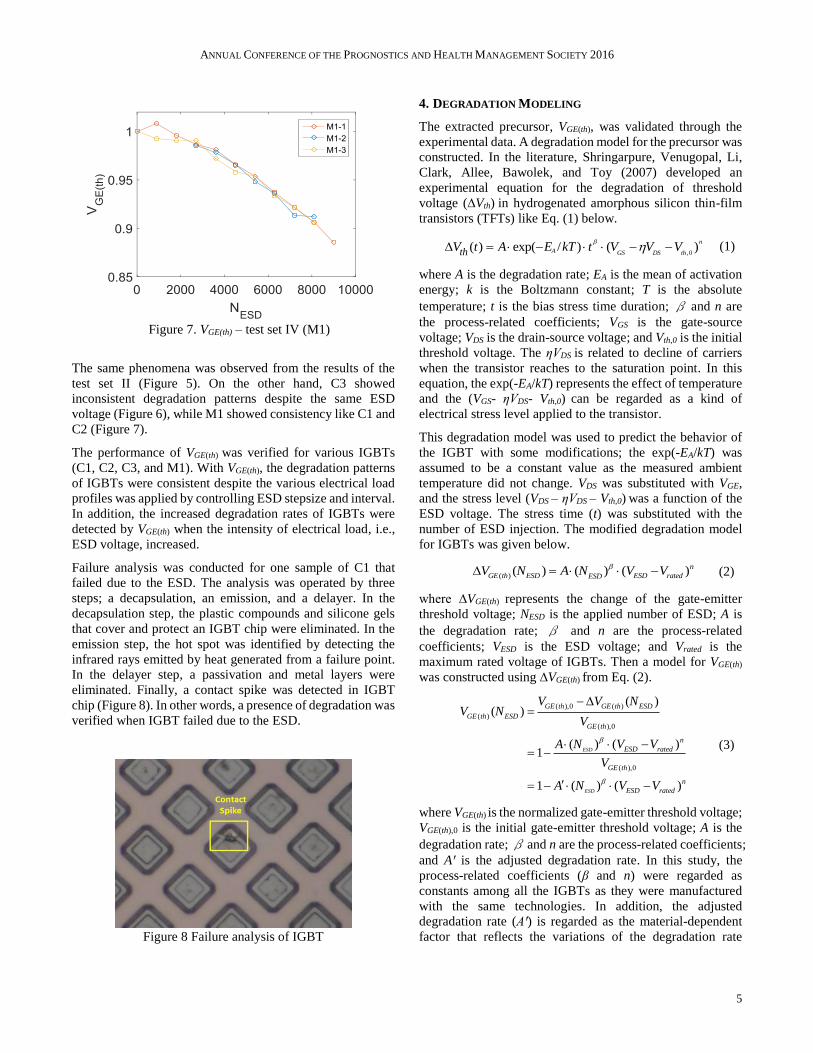
Figure 7. VGE(th) – test set IV (M1)
The same phenomena was observed from the results of the
test set II (Figure 5). On the other hand, C3 showed
inconsistent degradation patterns despite the same ESD
voltage (Figure 6), while M1 showed consistency like C1 and
C2 (Figure 7).
The performance of VGE(th) was verified for various IGBTs
(C1, C2, C3, and M1). With VGE(th), the degradation patterns
of IGBTs were consistent despite the various electrical load
profiles was applied by controlling ESD stepsize and interval.
In addition, the increased degradation rates of IGBTs were
detected by VGE(th) when the intensity of electrical load, i.e.,
ESD voltage, increased.
Failure analysis was conducted for one sample of C1 that
failed due to the ESD. The analysis was operated by three
steps; a decapsulation, an emission, and a delayer. In the
decapsulation step, the plastic compounds and silicone gels
that cover and protect an IGBT chip were eliminated. In the
emission step, the hot spot was identified by detecting the
infrared rays emitted by heat generated from a failure point.
In the delayer step, a passivation and metal layers were
eliminated. Finally, a contact spike was detected in IGBT
chip (Figure 8). In other words, a presence of degradation was
verified when IGBT failed due to the ESD.
Figure 8 Failure analysis of IGBT
4. DEGRADATION MODELING
The extracted precursor, VGE(th), was validated through the
experimental data. A degradation model for the precursor was
constructed. In the literature, Shringarpure, Venugopal, Li,
Clark, Allee, Bawolek, and Toy (2007) developed an
experimental equation for the degradation of threshold
voltage (∆Vth) in hydrogenated amorphous silicon thin-film
transistors (TFTs) like Eq. (1) below.
,0
( ) exp( / ) ( )n
A GS DS ththV t A E kT t V V V
(1)
where A is the degradation rate; EA is the mean of activation
energy; k is the Boltzmann constant; T is the absolute
temperature; t is the bias stress time duration; β and n are
the process-related coefficients; VGS is the gate-source
voltage; VDS is the drain-source voltage; and Vth,0 is the initial
threshold voltage. The ηVDS is related to decline of carriers
when the transistor reaches to the saturation point. In this
equation, the exp(-EA/kT) represents the effect of temperature
and the (VGS- ηVDS- Vth,0) can be regarded as a kind of
electrical stress level applied to the transistor.
This degradation model was used to predict the behavior of
the IGBT with some modifications; the exp(-EA/kT) was
assumed to be a constant value as the measured ambient
temperature did not change. VDS was substituted with VGE,
and the stress level (VDS – ηVDS – Vth,0) was a function of the
ESD voltage. The stress time (t) was substituted with the
number of ESD injection. The modified degradation model
for IGBTs was given below.
( ) ( ) ( ) ( )n
GE th ESD ESD ratedESDV N A N V V
(2)
where ∆VGE(th) represents the change of the gate-emitter
threshold voltage; NESD is the applied number of ESD; A is
the degradation rate; β and n are the process-related
coefficients; VESD is the ESD voltage; and Vrated is the
maximum rated voltage of IGBTs. Then a model for VGE(th)
was constructed using ∆VGE(th) from Eq. (2).
( ),0 ( )
( )
( ),0
( ),0
( )( )
( ) ( )1
1 ( ) ( )
ESD
ESD
GE th GE th ESD
GE th ESD
GE th
n
ESD rated
GE th
n
ESD rated
V V NV N
V
A N V V
V
A N V V
(3)
where VGE(th) is the normalized gate-emitter threshold voltage;
VGE(th),0 is the initial gate-emitter threshold voltage; A is the
degradation rate; β and n are the process-related coefficients;
and Aꞌ is the adjusted degradation rate. In this study, the
process-related coefficients (β and n) were regarded as
constants among all the IGBTs as they were manufactured
with the same technologies. In addition, the adjusted
degradation rate (Aꞌ) is regarded as the material-dependent
factor that reflects the variations of the degradation rate
Page 6
ANNUAL CONFERENCE OF THE PROGNOSTICS AND HEALTH MANAGEMENT SOCIETY 2016
6
among the manufacturing companies. After we fitted Aꞌ, β, n
based on the data sets of C1 and C2, the Aꞌ for C3 and M1
were fitted with the constant β, n.
A fitted curve using C1 and C2 was illustrated in Figure 9 and
the fitting results were clarified in Table 5. The mean values
of Aꞌ, β, n within 95% confidence bounds were 4.744×10⁻¹⁰,
1.539, and 0.676 respectively, and the R-squared value was
0.9965. The model was validated with high accuracy in terms
of R-squared value. Fitted curves for C3 and M1 were
illustrated in Figure 10 and the fitting results were clarified in
Table 6. Using the same β and n (1.539, 0.676), Aꞌ were fitted
to 3.839×10⁻¹¹ and 7.511×10⁻¹⁰ respectively. The models were
also validated with high accuracy in terms of R-squared value;
0.9933 and 0.9826. From the result, the hypothesis was
verified that the degradation behaviors of IGBTs with same
technology are consistent among the different companies. In
summary, the degradation of a trench gate field stop IGBT
subjected to ESD damage can be predicted using the
proposed degradation models with the degradation rate (Aꞌ)
fitted for the experimental results of the samples.
Figure 9. Orthogonal view of the Vth degradation model
fitted with C1 and C2 data
Table 5. The coefficients and R-squared value of Vth
degradation model fitted with C1 and C2
Coefficients (with 95% confidence bounds) R-squared value
Aꞌ 4.744×10⁻¹⁰ (3.682×10⁻¹⁰, 5.805×10⁻¹⁰)
0.9965 β 1.539 (1.522, 1.557)
n 0.676 (0.661, 0.690)
Table 6. The coefficients and R-squared values of Vth
degradation models fitted with C3 and M1 respectively
Aꞌ β n R2
C3 3.839×10⁻¹¹ 1.539 0.676
0.9933
M1 7.511×10⁻¹⁰ 0.9826
(a)
(b)
Figure 10. Orthogonal view of Vth degradation model: (a)
C3 and (b) M1
5. CONCLUSION
This paper determined the key failure precursor for IGBTs
subjected to electrical stresses. Then, the empirical model
was proposed to describe the evolution of the failure
precursor during the degradation. The main contribution of
this study is that the degradation of IGBTs that is modeled by
emulating the degradation of IGBTs. The degraded IGBTs
were prepared by injecting artificial faults of electrostatic
discharge (ESDs). The previous studies only compared the
conditions of normal IGBTs with the conditions of failed
ones.
The failure precursor VGE(th) for degradation of IGBTs
subjected to C-G ESD damage was identified and the
corresponding degradation model was constructed. The
performance of VGE(th) was verified using three sets of IGBTs
components and one set of IGBT modules. We concluded
that the proposed model properly describes the degradation
of IGBTs subjected to electrical stresses. In the future study,
another relevant precursor will be identified, and the
performance of the precursor will be validated in the case that
the IGBTs experience degradation by E-G ESD damage.
Page 7
ANNUAL CONFERENCE OF THE PROGNOSTICS AND HEALTH MANAGEMENT SOCIETY 2016
7
ACKNOWLEDGEMENT
This work was supported by grants from Hyundai NGV (Next
Generation Vehicle) through a program named as
“Development of prognostic technique for electronic
components in inverter system” by Hyundai Motor Group.
REFERENCES
Baliga, B. J., Adler, M. S., Love, R.P., Gray, P. V., &
Zommer, N. D. (1984). The insulated gate transistor: A
new three-terminal MOS-controlled bipolar power
device. IEEE Transactions on Electron Devices, 31 (6),
821-828. Doi:10.1109/T-ED.1984.21614
Celnikier Y., Benabou, L., Dupont, L., & Coquery, G. (2011).
Investigation of the heel crack mechanism in Al
connections for power electronics modules.
Microelectronics Reliability, 51 (5), 965-974.
doi:10.1016/j.microrel.2011.01.001
Jeong, J.-S., Hong, S.-H., & Park, S.-D. (2007). Field failure
mechanism and improvement of EOS failure of
integrated IGBT inverter modules. Microelectronics
Reliability, 47 (9-11), 1795-1799.
doi:10.1016/j.microrel.2007.07.087
Lee, J., Oh, H., Park, C. H., Youn, B. D., Kim, D. H., Kim,
B. H., & Cho, Y. U. (2016). Fault injection to insulated
gate bipolar transistor (IGBT) using electrostatic
discharge. Proceeding of Korean Society of Mechanical
Engineers (8), April 27-29, Busan, Korea.
Oh, H., Han, B., McCluskey, P., Han, C., & Youn, B. D.
(2015). Physics-of-failure, condition monitoring, and
prognostics of insulated gate bipolar transistor modules:
A review. IEEE Transactions on Power Electronics, 30
(5), 2413-2426. doi:10.1109/TPEL.2014.2346485
Patil, N., Celaya, J., Das, D., Goebel, K., & Pecht, M. (2009).
Precursor parameter identification for insulated gate
bipolar transistor (IGBT) prognostics. IEEE
Transactions on Reliability, 58 (2), 271-276.
doi:10.1109/TR.2009.2020134
Shringarpure, R., Venugopal, S., Li, Z., Clark, L. T., Allee,
D. R., Bawolek, E., & Toy, D. (2007). Circuit simulation
of threshold-voltage degradation in a-Si: H TFTs
fabricated at 175℃ . IEEE Transactions on Electron
Devices, 54 (7), 1781-1783.
doi:10.1109/TED.2007.899667
Wysocki, P., Vashchenko, V., Celaya, J., Saha, S., & Goebel,
K. (2009). Effect of electrostatic discharge on electrical
characteristics of discrete electronic components. Annual
Conference of the Prognostics and Health Management
Society (1-10), September 27-October 1, San Diego.
Yang, S., Bryant, A., Mawby, P., Xiang, D., Ran, L., &
Tavner, P. (2011). An industry-based survey of
reliability in power electronic converters. IEEE
Transactions on Industry Applications, 47 (3), 1441-
1451. Doi:10.1109/TIA.2011.2124436
Zhou, L., Zhou, S., and Xu, M. (2013). Investigation of gate
voltage oscillations in an IGBT module after partial bond
wires lift-off. Microelectronics Reliability, 53 (2), 282-
287. doi:10.1016/j.microrel.2012.08.024
Zhou, S., Zhou, L., and Sun, P. (2013). Monitoring potential
defects in an IGBT module based on dynamic changes
of the gate current. IEEE Transactions Power
Electronics, 28 (3), 1479-1487.
doi:10.1109/TPEL.2012.2210249