Excerpt from the Proceedings of the 2014 COMSOL Conference in Cambridge 3-D Multiphysics Model of Thermal Flow Sensors C. Falco 1, *, A. De Luca 1 , S. Safaz 1 , F. Udrea 1 1 University of Cambridge, 9 J.J. Thomson Avenue, Cambridge, CB30FA *C. Falco, 9 J.J. Thomson Avenue, Cambridge, UK, [email protected]Abstract: The aim of this work is to present a model capable to describe the behaviour of a thermal flow sensor under every physical aspect. A generic thermal flow sensor relates the flow properties with a variation in the temperature profile inside the device itself. Thus, it contains a resistive element biased with an external current to locally increase the temperature, surrounded by one or more temperature sensing elements. The analysis involves three different and coupled physic domains: electric current, heat transfer in solids and laminar flow. Once the model was ready, it has been used to model an existing SOI CMOS MEMS wall shear stress sensor. The results shows a perfect agreement with the experimental data under every condition, proving the validity of the model. Keywords: flow sensor, multiphysics, thermal sensor, laminar flow, electric current, heat transfer. 1. Introduction Fluid dynamic phenomena present a high complexity and non-linearity. An analytical description can be obtained only in few cases, and even then some assumptions are required to obtain the result. On the other hand, the numerical approach requires a really fine mesh to accurately follow the spatial profile of the involved variables. Coupling it with other physical phenomena enhance those problems. For this reason, the other attempts presented in literature are only 2- D [1] or consider only the Navier-Stokes equations [2] whereas this work couple them with joule heating and heat dissipation via conduction in a complete 3-D geometry. The model has been designed to resemble an SOI CMOS MEMS thermal flow sensor, presented in section 2. A detailed results comparison has been performed in order to validate it. Section 3 presents the three physics phenomena and their connections, together with the equations used by the model. The model itself will be presented under every aspect in section 4, including the differences with the real device and their effect on the results. The validation process is presented in section 5, the conclusions in section 6. 2. Validation Device The validation chip contains 5 parallel metal strips with dimension 2 μm × 400 μm × 0.3 μm. The central one is used to rise the device temperature up to 300 °C, and all of them can be used to sense the temperature via the relation between the metal resistivity and the absolute temperature. The resistance value is obtained with a 4-wires measure. The chip has been produced in a standard SOI CMOS technology, and required only one post-processing step: a deep reactive ion etching at the back surface in order to remove the silicon substrate from underneath the sensing elements. This corresponds to a dramatic reduction in the thermal conductivity seen by the heating element and thus in the power needed to rise the temperature at the desired value. Figure 1 reports the device cross section (a) and top view (b). Fig 1 – Technology cross section (a) and top view (b) of the validation device. The red rectangle identify the region where the temperature profile is evaluated.
Transcript
Excerpt from the Proceedings of the 2014 COMSOL Conference in Cambridge
3-D Multiphysics Model of Thermal Flow Sensors C. Falco1,*, A. De Luca1, S. Safaz1, F. Udrea1 1University of Cambridge, 9 J.J. Thomson Avenue, Cambridge, CB30FA *C. Falco, 9 J.J. Thomson Avenue, Cambridge, UK, [email protected] Abstract: The aim of this work is to present a model capable to describe the behaviour of a thermal flow sensor under every physical aspect. A generic thermal flow sensor relates the flow properties with a variation in the temperature profile inside the device itself. Thus, it contains a resistive element biased with an external current to locally increase the temperature, surrounded by one or more temperature sensing elements. The analysis involves three different and coupled physic domains: electric current, heat transfer in solids and laminar flow. Once the model was ready, it has been used to model an existing SOI CMOS MEMS wall shear stress sensor. The results shows a perfect agreement with the experimental data under every condition, proving the validity of the model. Keywords: flow sensor, multiphysics, thermal sensor, laminar flow, electric current, heat transfer. 1. Introduction
Fluid dynamic phenomena present a high complexity and non-linearity. An analytical description can be obtained only in few cases, and even then some assumptions are required to obtain the result.
On the other hand, the numerical approach requires a really fine mesh to accurately follow the spatial profile of the involved variables. Coupling it with other physical phenomena enhance those problems. For this reason, the other attempts presented in literature are only 2-D [1] or consider only the Navier-Stokes equations [2] whereas this work couple them with joule heating and heat dissipation via conduction in a complete 3-D geometry.
The model has been designed to resemble an SOI CMOS MEMS thermal flow sensor, presented in section 2. A detailed results comparison has been performed in order to validate it.
Section 3 presents the three physics phenomena and their connections, together with the equations used by the model. The model
itself will be presented under every aspect in section 4, including the differences with the real device and their effect on the results.
The validation process is presented in section 5, the conclusions in section 6. 2. Validation Device
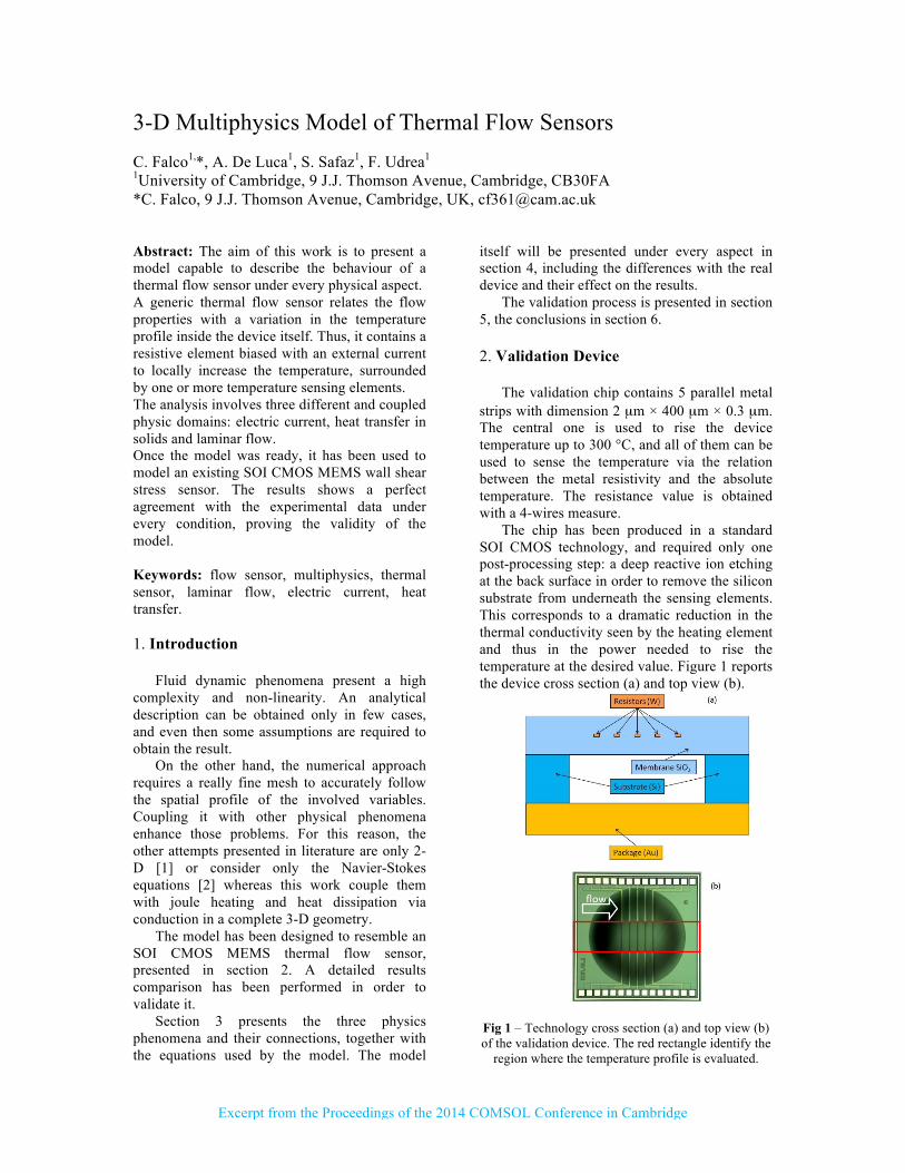
The validation chip contains 5 parallel metal strips with dimension 2 µm × 400 µm × 0.3 µm. The central one is used to rise the device temperature up to 300 °C, and all of them can be used to sense the temperature via the relation between the metal resistivity and the absolute temperature. The resistance value is obtained with a 4-wires measure.
The chip has been produced in a standard SOI CMOS technology, and required only one post-processing step: a deep reactive ion etching at the back surface in order to remove the silicon substrate from underneath the sensing elements. This corresponds to a dramatic reduction in the thermal conductivity seen by the heating element and thus in the power needed to rise the temperature at the desired value. Figure 1 reports the device cross section (a) and top view (b).
Fig 1 – Technology cross section (a) and top view (b) of the validation device. The red rectangle identify the
region where the temperature profile is evaluated.
Excerpt from the Proceedings of the 2014 COMSOL Conference in Cambridge
3. Numerical Model
The numerical model, to be accurate, has to be as similar as possible to the actual device. Nonetheless, some approximations can have an impact in the mesh count without affecting the results: • The metal pads are placed above the
substrate, where the temperature can be assumed constant. Thus, the change in thermal conductivity induced by the metal does not affect the final results and can be neglected;
• The voltmetric contact wires used to sense the resistance are thin (2 µm), really close to the wide amperometric ones (20 µm wide) and has a really low current flowing in them. Thus, they have no effect on both the heat generation and dissipation and thus are not included. On the other hand, it is not possible to ignore
the packaging since it introduces a thermal resistance of 22 W/K on the heat dissipation path, causing an error in the temperature profile as high as 10%.
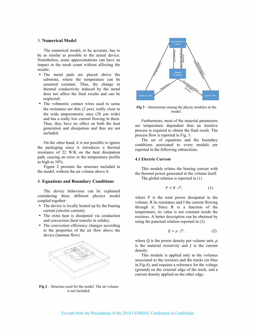
Figure 2 presents the structure included in the model, without the air volume above it.
4. Equations and Boundary Conditions
The device behaviour can be explained considering three different physics model coupled together: • The device is locally heated up by the biasing
current (electric current); • The extra heat is dissipated via conduction
and convection (heat transfer in solids); • The convection efficiency changes according
to the properties of the air flow above the device (laminar flow).
Fig 2 – Structure used for the model. The air volume is not included.
Fig 3 – Interactions among the physic modules in the
model. Furthermore, most of the material parameters
are temperature dependent thus an iterative process is required to obtain the final result. The process flow is reported in Fig. 3.
The set of equations and the boundary conditions associated to every module are reported in the following subsections.
4.1 Electric Current
This module relates the biasing current with the thermal power generated in the volume itself.
The global relation is reported in (1)
𝑃 = 𝑅 ⋅ 𝐼!, (1)
where P is the total power dissipated in the volume, R its resistance and I the current flowing through it. Since R is a function of the temperature, its value is not constant inside the resistors. A better description can be obtained by using the punctual relation reported in (2)
𝑄 = 𝜌 ⋅ 𝐽!, (2)
where Q is the power density per volume unit, 𝜌 is the material resistivity and 𝐽 is the current density.
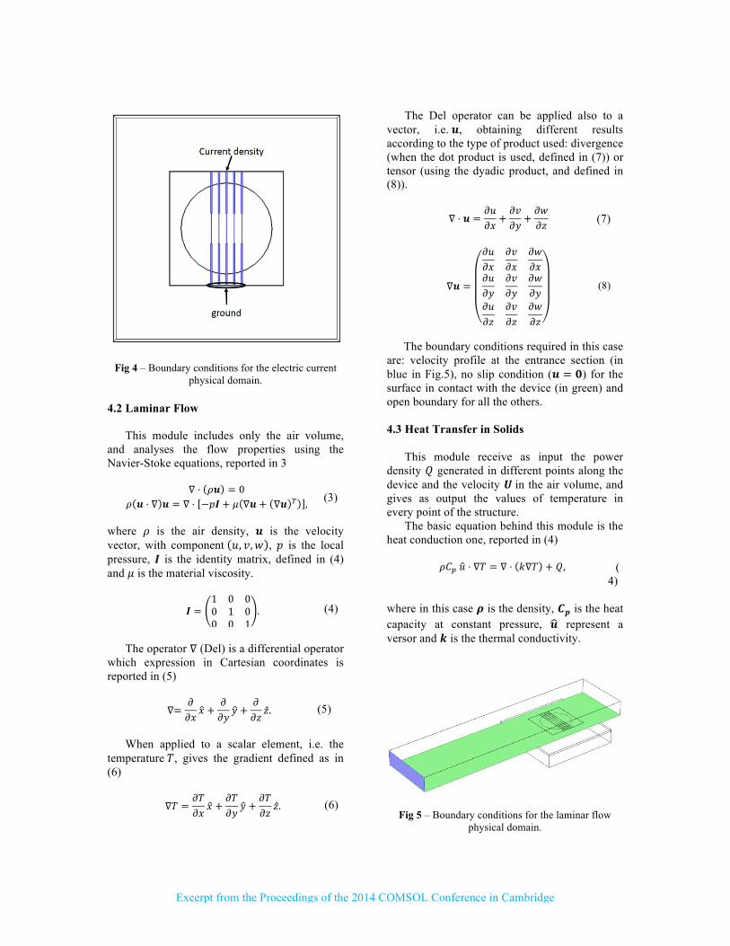
This module is applied only to the volumes associated to the resistors and the tracks (in blue in Fig.4), and requires a reference for the voltage (ground) on the external edge of the track, and a current density applied on the other edge.
Excerpt from the Proceedings of the 2014 COMSOL Conference in Cambridge
Fig 4 – Boundary conditions for the electric current physical domain.
4.2 Laminar Flow
This module includes only the air volume,
and analyses the flow properties using the Navier-Stoke equations, reported in 3
∇ ⋅ 𝜌𝒖 = 0
𝜌 𝒖 ⋅ ∇ 𝒖 = ∇ ⋅ −𝑝𝑰 + 𝜇 ∇𝒖 + ∇𝒖 ! ,
(3)
where 𝜌 is the air density, 𝒖 is the velocity vector, with component 𝑢, 𝑣,𝑤 , 𝑝 is the local pressure, 𝑰 is the identity matrix, defined in (4) and 𝜇 is the material viscosity.
𝑰 =1 0 00 1 00 0 1
.
(4)
The operator ∇ (Del) is a differential operator
which expression in Cartesian coordinates is reported in (5)
∇=
𝜕𝜕𝑥𝑥 +
𝜕𝜕𝑦
𝑦 +𝜕𝜕𝑧𝑧.
(5)
When applied to a scalar element, i.e. the
temperature 𝑇, gives the gradient defined as in (6)
∇𝑇 =
𝜕𝑇𝜕𝑥
𝑥 +𝜕𝑇𝜕𝑦
𝑦 +𝜕𝑇𝜕𝑧𝑧.
(6)
The Del operator can be applied also to a vector, i.e. 𝒖, obtaining different results according to the type of product used: divergence (when the dot product is used, defined in (7)) or tensor (using the dyadic product, and defined in (8)).
∇ ⋅ 𝒖 =
𝜕𝑢𝜕𝑥
+𝜕𝑣𝜕𝑦
+𝜕𝑤𝜕𝑧
(7)
∇𝒖 =
𝜕𝑢𝜕𝑥
𝜕𝑣𝜕𝑥
𝜕𝑤𝜕𝑥
𝜕𝑢𝜕𝑦
𝜕𝑣𝜕𝑦
𝜕𝑤𝜕𝑦
𝜕𝑢𝜕𝑧
𝜕𝑣𝜕𝑧
𝜕𝑤𝜕𝑧
(8)
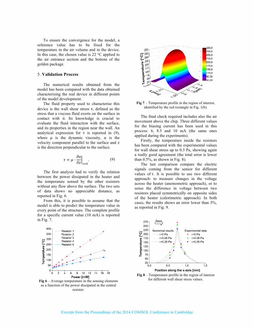
The boundary conditions required in this case
are: velocity profile at the entrance section (in blue in Fig.5), no slip condition (𝒖 = 𝟎) for the surface in contact with the device (in green) and open boundary for all the others.
4.3 Heat Transfer in Solids
This module receive as input the power
density 𝑄 generated in different points along the device and the velocity 𝑼 in the air volume, and gives as output the values of temperature in every point of the structure.
The basic equation behind this module is the heat conduction one, reported in (4)
𝜌𝐶! 𝑢 ⋅ ∇𝑇 = ∇ ⋅ 𝑘∇𝑇 + 𝑄, (
4) where in this case 𝝆 is the density, 𝑪𝒑 is the heat capacity at constant pressure, 𝒖 represent a versor and 𝒌 is the thermal conductivity.
Fig 5 – Boundary conditions for the laminar flow physical domain.
Excerpt from the Proceedings of the 2014 COMSOL Conference in Cambridge
To ensure the convergence for the model, a reference value has to be fixed for the temperature in the air volume and in the device. In this case, the chosen value is 22 °C applied to the air entrance section and the bottom of the golden package. 5. Validation Process
The numerical results obtained from the model has been compared with the data obtained characterising the real device in different points of the model development.
The fluid property used to characterise this device is the wall shear stress τ, defined as the stress that a viscous fluid exerts on the surface in contact with it. Its knowledge is crucial to evaluate the fluid interaction with the surface, and its properties in the region near the wall. An analytical expression for 𝜏 is reported in (9), where 𝜇 is the dynamic viscosity, 𝑢 is the velocity component parallel to the surface and 𝑧 is the direction perpendicular to the surface.
𝜏 = 𝜇 ⋅𝜕𝑢𝜕𝑧 !!!
.
(9)
The first analysis had to verify the relation
between the power dissipated in the heater and the temperature sensed by the other resistors without any flow above the surface. The two sets of data shows no appreciable distance, as reported in Fig. 6.
From this, it is possible to assume that the model is able to predict the temperature value in every point of the structure. The complete profile for a specific current value (10 mA) is reported in Fig. 7.
Fig 6 – Average temperature in the sensing elements as a function of the power dissipated in the central
resistor.
Fig 7 – Temperature profile in the region of interest,
identified by the red rectangle in Fig. 1(b). The final check required includes also the air
movement above the chip. Three different values for the biasing current has been used in this process: 6, 8.5 and 10 mA (the same ones applied during the experiments).
Firstly, the temperature inside the resistors has been compared with the experimental values for wall shear stress up to 0.3 Pa, showing again a really good agreement (the total error is lower than 0.5%, as shown in Fig. 8).
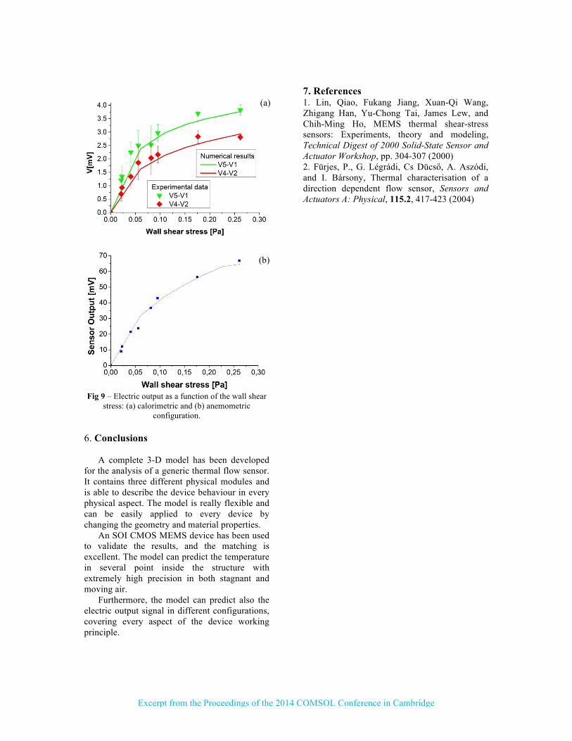
The last comparison compare the electric signals coming from the sensor for different values of 𝜏. It is possible to use two different approach: to measure changes in the voltage across the heater (anemometric approach), or to sense the difference in voltage between two resistors placed symmetrically on opposite sides of the heater (calorimetric approach). In both cases, the results shows an error lower than 5%, as reported in Fig. 9.
Fig 8 – Temperature profile in the region of interest
for different wall shear stress values.
Excerpt from the Proceedings of the 2014 COMSOL Conference in Cambridge
Fig 9 – Electric output as a function of the wall shear
stress: (a) calorimetric and (b) anemometric configuration.
6. Conclusions
A complete 3-D model has been developed for the analysis of a generic thermal flow sensor. It contains three different physical modules and is able to describe the device behaviour in every physical aspect. The model is really flexible and can be easily applied to every device by changing the geometry and material properties.
An SOI CMOS MEMS device has been used to validate the results, and the matching is excellent. The model can predict the temperature in several point inside the structure with extremely high precision in both stagnant and moving air.
Furthermore, the model can predict also the electric output signal in different configurations, covering every aspect of the device working principle.
7. References 1. Lin, Qiao, Fukang Jiang, Xuan-Qi Wang, Zhigang Han, Yu-Chong Tai, James Lew, and Chih-Ming Ho, MEMS thermal shear-stress sensors: Experiments, theory and modeling, Technical Digest of 2000 Solid-State Sensor and Actuator Workshop, pp. 304-307 (2000) 2. Fürjes, P., G. Légrádi, Cs Dücső, A. Aszódi, and I. Bársony, Thermal characterisation of a direction dependent flow sensor, Sensors and Actuators A: Physical, 115.2, 417-423 (2004)