Y ield M anagement Y ield M anagement Yield Acceleration Strategies for the Semiconductor Industry S O L U T I O N S Yield Acceleration Strategies for the Semiconductor Industry V O L U M E 3 I S S U E 3 FA L L 2001 $5.00 US S O L U T I O N S 15 COVER STORY — AN AUTOMATED METHOD FOR O VERLAY SAMPLE P LAN O PTIMIZATION 38 E FFECTIVE DEFECT MANAGEMENT IN THE LITHOGRAPHY CELL 50 SPECTROSCOPIC C RITICAL DIMENSION (SCD) M ETROLOGY FOR CD C ONTROL AND STEPPER C HARACTERIZATION 15 COVER STORY — A N A UTOMATED METHOD FOR O VERLAY SAMPLE P LAN O PTIMIZATION 38 E FFECTIVE DEFECT MANAGEMENT IN THE L ITHOGRAPHY CELL 50 SPECTROSCOPIC C RITICAL DIMENSION (SCD) M ETROLOGY FOR CD C ONTROL AND STEPPER C HARACTERIZATION SPECIAL ISSUE: A Focus on Lithography SPECIAL ISSUE: A Focus on Lithography
Transcript
Yield ManagementYield ManagementYield Acceleration Strategies for the Semiconductor Industry
S O L U T I O N SYield Acceleration Strategies for the Semiconductor Industry
VO L U M E 3 IS S U E 3 FA L L 2001 $5.00 US
S O L U T I O N S
15 COVER STORY —AN AUTOMATED METHOD FOR
OVERLAY SAMPLE PLAN OPTIMIZATION
38 EFFECTIVE DEFECT MANAGEMENT IN
THE LITHOGRAPHY CELL
50 SPECTROSCOPIC CRITICAL DIMENSION
(SCD) METROLOGY FOR CD CONTROL
AND STEPPER CHARACTERIZATION
15 COVER STORY —AN AUTOMATED METHOD FOR
OVERLAY SAMPLE PLAN OPTIMIZATION
38 EFFECTIVE DEFECT MANAGEMENT IN
THE LITHOGRAPHY CELL
50 SPECTROSCOPIC CRITICAL DIMENSION
(SCD) METROLOGY FOR CD CONTROL
AND STEPPER CHARACTERIZATION
SPECIAL ISSUE:A Focus on LithographySPECIAL ISSUE:A Focus on Lithography
Fall 2001 Yield Management Solutions2
C O N T E N T S
S p e c i a l F o c u s
C o v e r S t o r y
15 An Automated Method for Overlay Sample-Plan Optimization
Tighter design rules and process complexitieshave made effective sample planning anecessity for today’s fabs. Through quantita-tive analysis and modeling, this paperdemonstrates an automated and systematicapproach to identifying the optimal sampleplan. Validated with fab results, the method-ology proves to be successful not only inimproving stepper control accuracy, but alsoin reducing yield loss and unnecessaryrework.
Cover image by Mike Garnicaand Carlos Hueso, KLA-Tencor
6 UV Inspection of EUV and EPL Reticles
Inspection of EUV and EPL reticles pose severaltechnical challenges and risks to today’s maskmakers. This study demonstrates the feasibility ofoptical inspection of Next Generation Lithography(NGL) reticles at the 100 to 140 nm nodes, and offers recommendations for changes in maskdesign that can optimize their inspectability.
25 A Defect-to-Yield Cor relation Study forMarginally Printing Reticle Defects
Reticle defects can play a significant role in over-all device yield; however, some marginally printingmask errors may not actually result in yield loss.The challenge is to detect and quantify the impact of these marginally printing reticle defects.This study examines several available methods.
32 Investigation of 193 nm Resist ShrinkageDuring CD SEM Measurements193 nm resists are known to shrink during CDSEM measurements. The large size and non-linearbehavior of this shrinkage must be characterizedand understood if CD SEM metrology is to becorrectly applied in advanced lithography pro-cessing. This paper describes a study in whichrecommendations for the best measurement conditions were developed, along with speculationson possible models for the observed shrinkagemechanisms.
38 Effective Defect Management in the LithographyCellTechnology advances within the lithography areaare placing greater demands on defect manage-ment. The introduction of sub-wavelength, low κ1-lithography has shrunk the size of the focus-exposureprocess window and thus has placed tighter con-straints on absolute tool stability within the litho cell.Effective defect management is critical when newp rocesses are combined with these strict operatingc o n d i t i o n s.
Fall 2001 Yield Management Solutions 3
F A L L 2 0 0 1
S e c t i o n s
4 Editorial: The Changing Role of Inspectionand Metrology in Lithography
12 Yield Management Seminar Series
24 Spotlight on Lithography
49 Got a Litho Question? Ask the Experts
62 KLA-Tencor Trade Show Calendar
P r o d u c t N e w s
64 AIT XPH i g h - t h roughput scanning for inspecting patterned wafers
Surfscan SP1 DLS
Unpatterned-wafer inspection system for 0.13 and0.10 µm design rules
65 iADCInline Automatic Defect Classification Component ofIMPACT XP
SpectraCDNon-destructive Critical Dimension Metrology System
66 PRECICEIn-situ Film-Thickness and End-Point Control for Cu CMP
ASET-F5x Wafer Bow Wafer Stress Capability(WBWS)Film and Stress Metrology for 300 mm Monitor Wa f e r s
reproduced without permission from KLA-Tencor Corporation.
Products in this document are identified by trademarks of their respective
companies or organizations.
38 5025
50 Spectroscopic Critical Dimension (SCD™) Metrology for CD Control and StepperCharacterizationSmaller device dimensions and tighter processcontrol windows force CD metrology tools todetect and measure changes in feature profilesthat are becoming critical to inline processc o n t rol and stepper evaluation for sub-0.18 µmtechnology. Spectroscopic CD is an opticalmetrology technique that can address theseneeds.
56 Using Pattern Quality Confi rmation toControl a Metal-Level DUV Process With aTop-Down CD SEMAs critical-feature patterning processes incre a s ein complexity and sensitivity, conventional CDmeasurements may not afford the level ofprocess control required for effective deviceproduction. By comparing recorded top-downSEM images to a predefined reference image,Pattern Quality Confirmation (pQC) enables amore detailed analysis of measurements cap-tured by KLA-Tencor 8xxx series CD SEMs.
Fall 2001 Yield Management Solutions4
EditorialS E C T I O N S
Metrology and inspection have been called “non-value-added” operations in the past, but it is clear that anyfab that does not use these tools effectively will see sig-nificant losses in yield, bin-sort performance, scrap, andrework. Inspection and metrology’s role has becomeone of “non-value-subtracted,” as well as one of realvalue added.
Like defect inspection, metrology is a strategic weaponfor competitiveness, and for process capability and viability. Especially in lithography, where the smalland shrinking process window creates challenges inmanufacturability, a fab must view metrology as part of the overall lithography system.1 Metrology providesthe visibility to understand where the optimum processlies, and where it is moving.
Inspection and measurement provide information thathelps engineering to map out the process’s responsesurface, and also provides confidence in the shape ofthat surface. This provides the context for yield learn-ing, which is defined as yield improvement rate, or thechange in average yield over a period of time, typicallyone month. (This may also be applied to rework orscrap.) To positively and predictably impact yield, theprocess engineer must understand the componentswhich contribute to yield loss. The best practicesamong fabs include a prioritization of the yield detrac-tors, and then focussing on improving or fixing the topdetractors. It is only by reducing the impact of each
The Changing Role of Metrologyand Inspection in Lithography
(and moving it to the end of the Pareto chart) that pre-dictable progress can be made.
In the case of metrology, it is also essential to define abudget. For example, many fabs are struggling to fittheir process into a 40 nm or 50 nm overlay budget,without a full understanding of each component of thebudget. As described above, with the budget defined(along with the proper way to statistically combine thecomponents), it then becomes easy and obvious whereto focus improvement resources.
This issue of the Yield Management Solutions magazineillustrates many of the ways that inspection and metrologyare used in lithography and other process modules tobring the process into focus, and to assist in improvingit, with great economic benefit for the fab.
Overlay is proving to be one of the major challengesfor 0.13 µm design rules (not to mention for 0.18 µm).KLA-Tencor, working with several fabs, has identifiedthe impact of improper sampling for overlay estimation.In some cases, common (improper) sampling across awafer can consume 25 nm out of a 40 nm budget, andcan cause several percentage points of yield loss!However, by doing a proper systematic analysis, thissampling bias can be reduced below 10 nm or less.
Defect issues in the litho cell are well beyond the pointwhere manual inspection can provide useful information.While defect reduction methodologies are well estab-lished in all other process modules in the fab, lithographyhas lagged in best practices for defect yield learning;1 Ashkenaz, Scott, editorial in YMS Summer 2000, Vol 2, Issue 3
Fall 2001 Yield Management Solutions 5
S O L U T I O N SYield Management
C O R P O R AT E H E A D Q U A RT E R SKLA-Tencor Corporation160 Rio RoblesSan Jose, California 95134408.875.3000
I N T E R N AT I O N A L O F F I C E SKLA-Tencor France SARLEvry Cedex, France33 16 936 6969
KLA-Tencor LimitedWokingham, United Kingdom44 118 936 5700
ED I T O R- I N- CH I E FUma Subramaniam
MA N A G I N G ED I T O RSiiri Tuckwood
CO N T R I B U T I N G ED I T O R SScott AshkenazAparjot DehalIndira RangarajanDave HattorimanabeTom Salinas
ART DI R E C T O R A N D
PR O D U C T I O N MA N A G E RCarlos Hueso
DE S I G N CO N S U LTA N TMichael Garnica
CI R C U L AT I O N ED I T O RRolando Gonzalez
KLA-Tencor Worldwide
The Editors
Yield ManagementS O L U T I O N S
this is in part due to the ongoing reliance on manual inspection. Fabs that haveimplemented photocell monitoring (PCM) and macro ADI, along with defect reduction methods, have seen dramatic improvements in overall manufacturing costs.
Another area where metrology can provide significant cost benefit is in offloadingtime-consuming and costly self-test operations of process tools. KLA-Tencor andASML have worked together to provide a solution that reduces the non-productivetime of the stepper/scanner, resulting in higher litho cell productivity, without significant impact on metrology productivity.
While inspection and metrology do help to identify and lessen the impact of processexcursions by providing quick response, they also are now essential i n m a k i n g p r o g r e s swith yield learning. It is through the intelligent application of cost-optimized sampling and the structure of proper process models, that the process engineer mayidentify critical defects or variation sources, identify their causes, and move themlower in the Pareto chart. Without these tools, analyses and actions, manufacturingcosts would be higher. The best-known methods described in this issue show howinspection and metrology have become “non-value-subtracted.”
Fall 2001 Yield Management Solutions6
LithographyS P E C I A L F O C U S
The emphasis to date in this program has been on providing feedback to mask makers so that mask designcan be optimized for inspection. A number of NGLreticles have been imaged with a specially modified UVinspection system. Based on images and simulationresults, recommendations have been made for changesin mask design that can improve the inspectability ofNGL masks. Images and preliminary inspection resultson some NGL masks will be presented in this paper.Simulations have been carried out which indicate thatEUV masks can be optimized for inspectability. In particular, the absorber reflectivity at the inspectionwavelength should be minimized, and the buffer layerthickness can be chosen to improve contrast.
Research tool descriptionThe research tool used in these studies is based on aKLA-Tencor high-NA UV inspection system. Theoperating wavelength is 364 nm, with a minimum pixelsize of 150 nm. The system has been modified to acceptall NGL reticle types. Due to the fact that NGL r e t i c l e sdo not have pellicles, special care has to be taken to avoidcontaminants. A reticle SMIF pod developed by AsystTechnologies can be used to keep the reticles clean whennot undergoing inspection. A transfer station has beenbuilt to transfer reticles from the SMIF pod to s p e c i a l
UV Inspection of EUV and EPL ReticlesDonald W. Pettibone, KLA-Tencor CorporationAlan R. Stivers, Components Research, Intel CorporationP. J. S. Mangat, Motorola *DigitalDNA™ LaboratoriesMichael Lercel, NGL MCoC, Photronics/IBMAnthony Novembre, Bell Laboratories, Lucent Technologies
A UV inspection tool has been used to image and inspect Next Generation Lithography (NGL) reticles. Inspection imagesand simulations have been used to provide feedback to mask makers so that inspectability of NGL masks can be optimized.SCALPEL masks have high optical contrast and look much the same in reflection as conventional chrome-on-glass masksdo in transmission. EPL stencil masks can be imaged well in reflection, but defects below the top surface (in the cutouts)may not be detectable optically. EUV masks made to date tend to have relatively low contrast, with line edge profiles thatare complex due to interference effects. Simulation results show that improved EUV inspection images can be obtained witha low reflectivity absorbing layer and the proper choice of buffer layer thickness.
IntroductionA partnership, partially sponsored byNIST-ATP Cooperative Agreement#70NANB8H44024, has been formed toretire the technical risks associated withoptical inspection of EUV and SCALPELreticles. The members of this partnershipare KLA-Tencor, Lucent Technologies, the EUV-LLC, Photronics, and DupontPhotomasks. The EUV-LLC is comprised ofAMD, Infineon, Intel, Micron, andM o t o r o l a . In addition, Motorola has provid-ed SCALPEL masks to the program.
This program has three phases, each aboutone year in duration. In the first year,KLA-Tencor built a research tool and gathered information to support modelingefforts. In this, the second year, we areimaging and inspecting NGL reticles. Themain goal this year is to establish the feasibility of optical inspection of NGL reticles at the 70 and 100 nm nodes. In the third year, KLA-Tencor plans to designa production prototype inspection systemfor NGL reticles.
of both resolution and image intensity, with up to 75percent loss of light at a corner of two intersectingstruts. Therefore, reflection imaging from the front sideof the mask is the preferred inspection mode for verti-cal strut SCALPEL masks.
We report here inspection results for three SCALPELmasks. The first, SCALPEL1, designed and fabricatedby Lucent Technologies, is made up of a stack of 27 nmof Won six nm of Cr on a 100 nm SiNx membrane,with the substrate being a four-inch silicon wafer. Thestruts are formed by an anisotropic, wet potassiumhydroxide etching of <100> Silicon wafers. The mem-branes are 1.1 mm by 12.1 mm on a side. The base pat-tern of this programmed defect mask is a wiring patterncomprised of 3.0-micron lines and spaces. There arethree types of defects: a bridge between lines, a breakof a line, and a pindot between lines, at seven differentnominal sizes ranging from 200 nm to 800 nm in 100nm increments.
Figure 2 shows reflection and transmission images of thesmallest pindot. The contrast of the defect observed inr e fle c t i on mo de is ab o ut tw i ce th at ob s e r v ed in tr a n s m i s s i o n .The wiring pattern exhibits good contrast to noise in bothreflection and transmission. The line edge profiles aremonotonic, with no edge ringing in the reflection image.This is due to the fact that the SCALPEL mask stack isthin compared to a wavelength, about one-tenth of awavelength at UV. Inspection results are shown in Table 1.All but the smallest defects were found consistently inthe six transmission inspections that were run.
Fall 2001 Yield Management Solutions 7
F i g u re 2. UV images o f Lucent SCALPEL mask with 200 nm nominal
pindot defect.
S P E C I A L F O C U S
adapters that are mounted in the inspection tool. Newc o m p u t i n g capabilities have been added to the researchtool, resulting in improved defect sensitivity, which isn e e d e d to meet the defect sensitivity requirements ofNGL.
NGL images and inspection resultsSCALPELSCALPEL (Scattering with Angular LimitationProjection Electron-beam Lithography) is an ElectronProjection Lithography (EPL) technology developed byLucent Technologies1. The mask is constructed from a200 mm diameter silicon wafer on which a thin siliconrich nitride (SiNx) layer, typically 100 nm, and a metalscattering layer, typically 30 nm of tungsten (W) andchromium (Cr), are deposited. The silicon wafer is patterned and etched to produce areas of freestandingmembranes. The remaining silicon substrate forms agrillage structure and provides support and mechanicalstrength (Figure 1). The mask pattern is etched intothe metal (scatterer) layer and the mask is imaged intransmission by scanning a 1 mm x 1 mm 100 kVelectron beam along the membrane stripes, with adja-cent stripes being stitched together at the wafer. Themask image is projected with 4X-reduction electronoptics onto a resist-coated wafer. At UV wavelengthsthe membrane is transparent, so defects on the backsideof the membrane are visible provided they are notbehind the metal pattern.
The SCALPEL masks that were tested had trapezoidalstruts that were wet etched. This permits inspection ineither reflection or transmission mode. However, it ishighly desirable to have vertical wall struts so as tomaximize the usable space on a mask, which will bebased on a 200 mm wafer when SCALPEL goes intoproduction. Vertical struts pose an inspection problemfor transmission imaging or for imaging from thebackside (strut side) of the mask, the front side of themask having the metal scatterer on it. This is becausethe vertical walls vignette the high-NA components ofthe light that are needed to obtain good resolution andhigh defect sensitivity. This results in spatial variations
F i g u re 1. SCALPEL mask layout and cross sect ion.
The second mask, SCALPEL2, was made by Photronics/MCoC. It has a programmed defect pattern designed byK L A - Tencor on a four-inch silicon wafer with trapezoidalstruts. The mask stack is 27 nm of W on five nm of Cron a 150 nm membrane of SiNx. There are 14 defecttypes at ten different defect sizes. Figure 3 shows aseries of pinhole defects in a wiring pattern of 400 nmlines and spaces, which would print on the wafer at100 nm lines and spaces. The nominal defect size inthese defects ranges from 80 nm to 320 nm in 80 nmincrements. The defect visibility is better in the reflec-tion images than in transmission.
The third mask, SCALPEL3, made by Motorola, hasthe same programmed defect pattern as SCALPEL2,though it also includes the patterns scaled to smallersizes. It is based on an eight-inch silicon wafer withtrapezoidal struts. The mask stack is 30 nm of tantalumsilicon nitride on 10 nm of Cr on a 100 nm SiNxmembrane. The base pattern shown in Figure 4 has200 nm lines and spaces, which would print as 50 nmlines and spaces on the wafer. The nominal defect sizein these defects ranges from 40 nm to 160 nm in 40nm increments. Again, better contrast is seen in thereflected images.
In summary, SCALPEL masks, in reflection, look muchthe same as conventional chrome on glass masks do intransmission. The programmed defects we have studiedto date show better visibility in reflection than intransmission. Programmed SCALPEL defects in the100 to 140 nm size range are visible.
EPL Stencil MasksOne type of EPL uses a stencil mask and images trans-mission electrons through the mask to the wafer with a4x reduction.2 H o w e v e r, unlike SCALPEL, which uses ascattering layer to obtain mask contrast, stencil cutoutsare made through a 2.0 µm thick silicon membrane to
obtain mask contrast. We have imaged one stencil maskmade by Photronics/MCoC (Figure 5). The reflectionimage of the top surface of the stencil mask shows goodcontrast and resolution. The transmission image showspoorer resolution and very low signal levels, on the orderof a few percent. Therefore, it is likely that stencil maskinspection may not be possible using an optical systembecause defects that are not near the top surface of the
mask may not be detectable at the needed sensitivitylevels. More work needs to be done to verify this.
EUV A general description of EUV lithography is providedin Reference 3. EUV masks are made at 4X, and arecomposed of an absorbing metal layer on top of a bufferlayer on top of an EUV reflecting mirror (Figure 6).This mirror is composed of alternating layers of Si andmolybdenum (Mo), and typically forty pairs of layersare used to obtain a reflectivity of approximately 65percent at the EUV wavelength of 13.4 nm. The bufferlayer is there to prevent damage to the multilayer duringthe absorber etch process and mask repair process.
The patterned EUV masks are first inspected for harddefects after the absorber etch. The defects are thenrepaired, and the buffer layer is subsequently etched. Asecond inspection is performed after the buffer layer isetched. The absorber and buffer layer height add up to anoptical path difference (OPD) of between approximately
S P E C I A L F O C U S
F i g u re 3. SCALPEL2 mask (Pho tronics/MCoC), defects A1, A3, A5,
A7, 400 nm L/S.F i g u re 4. SCALPEL3 mask (Motorola), defec ts A1, A3, A5, A7,
200 nm L/S.
F i g u re 5. Stencil mask (Photronics/MCoC), reflection and transmission
images, 400 nm line widths .
Reflection
Transmission,high contrast
Reflected
Transmitted
Reflected
Transmitted
40 nm 80 nm 120 nm 160 nmNominal Sizes
40 nm 80 nm 120 nm 160 nmNominal Sizes
120 nm to 180 nm, which is of the order of one-half ofthe UV or DUV inspection wavelength. Therefore, inr e flection inspection images, the OPD difference betweenlight reflected off of the absorber and light reflected offof the ML is about one wavelength. This rapid phasevariation typically results in a pronounced dark fringe inthe inspection image at the absorber-ML edges, unlessthe reflectivity of one of the materials is much higherthan the reflectivity of the other. This effect will bediscussed in the section on optimization of EUV masks.
The first mask we inspected, EUV1, was designed andmade by Intel, and has a programmed defect pattern withwiring and contact defects of varying types and sizes.The mask stack has 105 nm of titanium (Ti) absorber, on85 nm of silicon dioxide (SiO2) buffer layer, on a siliconwafer substrate. Silicon is a reasonably good match tothe EUV multilayer in terms of UV reflectance. TheSiO2 has been etched on this mask, so it is only presentunder the absorber layer. Figure 7 shows reflectionimages of an absorber protrusion defect in the 400nm/800 n m l i n e / s p a c e p a t t e r n. The d e f e c t is 0 . 5 - m i c r o n swide and protrudes into the space a distance of 80 nm,100 nm, 140 nm, and 200 nm. The Protrusion Adefect sizes have been confirmed with SEM measure-ments. Note that all of the defects are visible in theimages. The dark fringes mentioned earlier are evidentin these images. Inspection results for the 400/800l i n e / s p a c e p a t t e r n are shown in Table 2. Defects towardsthe bottom of the table that were not detected werechecked with a SEM. These defects were shown to beeither undersized or to have not resolved on the reticle at
all. For the defects that were well resolved on the reticle,we were able to repeatedly detect defects in the 100nm to 140 nm size range.
Another mask, EUV2, was made by Motorola. The maskstack is 30 nm of Cr on 100 nm of silicon oxynitride(SiON) on 10 nm of Cr, on a Si/Mo refle c t i v e multilayer.The buffer layer (SiON) has been etched. In Figure 8we present images of a 400 nm L/S test pattern. In thisimage a 4X blow-up of five lines is shown. Dark inter-ference fringes around the Cr absorber lines are evident.We used TEMPEST, a software program that solvesMaxwell’s equations for the case of monochromaticradiation incident upon a scattering structure in con-cert with aerial imaging software from PanoramicTechnology5, to calculate and simulate the UV inspec-tion image of EUV2. This simulated image is also shown in Figure 8, and we cansee that the dark fringes are predicted by the simulation.In the next section, these simulation tools are used tounderstand and optimize the absorber line edge profil e s ,leading to improved inspectability of the EUV masks.
Optimization of EUV masksWork in the area of optimizing EUV mask inspectabil-ity has been done by Tejnil and Stivers 6. This work hasfocused on finding materials with good contrast. In
F i g u re 6. EUV mask cross section.
F i g u re 7. EUV1 mask (Intel ), pro t rusion defect images.
F i g u re 8. EUV2 (Motorola) images and TEMPEST simulation, 400 nm L/S.
Table 2. EUV1 inspection results, 6 inspections, 400 nm lines/800 nms p a c e s .
4X Blowup
TEMPESTsimulation
Fall 2001 Yield Management Solutions 9
PA 08 PA10 PA14 PA20(80 x 500 nm) (100 x 500 nm) (140 x 500 nm) (200 x 500 nm)
Fall 2001 Yield Management Solutions10
addition to the mean contrast of the absorber materialbeing an important factor, the rapid phase ramp of ther e flected light due to the mask topography signific a n t l yimpacts the visibility of the absorber lines duringinspection. In Figure 9 we show simulated images froma set of absorber lines of varying width. The lines havea width of, from left to right, 50 nm, 100 nm, 200 nm,300 nm, 400 nm, and 500 nm. These simulations wererun with the absorbing material being either Cr or tita-nium nitride, and with an absorber height of 50 nm,with no buffer layer under the absorber. The Cr has ar e fle c t i v i t y of 0.66 (in thick sections) and the TiN has areflectivity of 0.22, both at a wavelength of 364 nm.The multilayer reflectivity has been taken to be 0.50.We can see how the edge interference changes theappearance of the line images. In the broad lines the Cris brighter than the multilayer, as expected from theirrelative contrast. As the line narrows, the dark fringesm e rge and we undergo a contrast reversal. This makesit difficult to interpret the images. The *ave greatervisibility than the Cr lines. Further simulations havebeen carried out which indicate that an absorber reflec-tivity of ten percent or less would be very desirable interms of improving the line visibility. Conventionalmasks that use Cr with an a n t i r e flection coating canachieve such a low refle c t i v i t y. It is worth noting that itis somewhat easier to find candidate absorber materialswith low reflectivity at DUV wavelengths than at UVwavelengths.
When the buffer layer is present, its thickness can beoptimized for maximum line image contrast. In Figure10 we show simulations of a constant width absorber
line on varying heights of buffer layer, ranging from 40 nm to 80 nm in 10 nm steps. We see that the visi-bility of the line is a strong function of the height ofthe buffer layer. This effect is easily explained by thereflected light interference that happens when a smallscatterer is positioned above a mirror that is normallyilluminated. Interference minima occur when the scat-terer is positioned at half-wave multiples above themirror, and maxima are a quarter-wave away. Thebuffer layer height is thus an important variable thatneeds to be controlled to optimize line visibility.
SummaryIn this paper we have demonstrated the feasibility ofoptical inspection of EUV and SCALPEL masks. Wehave imaged masks made by several sources and carriedout limited inspections of the masks that had pro-grammed defects. SCALPEL and EUV mask defects inthe range of 100 to 140 nm were consistently detected.In order to meet the stringent ITRS roadmap require-ments for defect sizes that are 80 nm at the 100 nmnode and 55 nm at the 70 nm node, we will extendthis work to DUV (257 nm wavelength) inspection inthe coming year. We will also optimize the defectdetection algorithms specifically for EUV andSCALPEL reticles to further improve sensitivity.
We have supported NGL mask development withimages and inspections from the research tool. A valu-able collaboration has been established that providesrapid feedback to the mask developers based on themask images and inspection results.
F i g u re 9. TEMPEST simulations of Ultraviolet High Resolution (UVHR) line profi les of absorbers of varying reflectivity and width.
S P E C I A L F O C U S
for work on the EUV1 mask and for helpful technicaldiscussions. Finally, we would like to thank Yalin Xiong,Jacobus Koster, and Matt DiLorenzo of KLA-TencorCorporation for their technical support of the researchtool used in this work.
References1 . J. A. Liddle, et al, “The SCALPEL Lithography System”,
Japan. J. Appl. Phys., 34, 12B, 6663 (1995).2 . Hans C. Pfeif f e r, “PREVAIL - IBM’s E-Beam Technology for
3. John E. Bjorkholm, “EUV Lithography - The Successor toOptical Lithography?”, Intel Technology Journal, Q3’98.
4. A l f red K. Wong, “Rigorous Three-dimensional Ti m e - D o-main F i n i t e - D i ff e rence Electromagnetic Simulation”, Ph.D.d i s s e r-tation, Engineering- Electrical Engineering andComputer Sciences, University of California at Berkeley,1 9 9 4 .
5 . Panoramic Te c h n o l o g y, www. p a n o r a m i c t e c h . c o m .6 . Edita Tejnil and Alan R. Stivers, Components Researc h ,
Intel Corporation, private communication.
A version of this ar ticle was originally published in SPIE Pro c e e d i n g s4186, pp. 250-258 (2001) entitled “UV Inspection of EUV and SCALPELReticles” by Donald W. Pettibone, Noah Bareket, KLA-Tencor Corporation;Ted Liang, Alan R. Stivers, Components Research, Intel Corporation; ScottD. Hector, P. J. S. Mangat, Motorola * DigitalDNA Labs.; D. J. Resnick, PSRLM o t o rola Labs.; Micheal Lercel, Mark Lawliss, Chris Magg, NGL M C o C ,P h o t ronics/IBMN; Anthony Novembre, Reginald Farro w, Bell Labs, Lucent Te c h n o l o g i e s .
Using simulation tools and inspection images, we havefound that EUV mask inspectability may be optimized.Specifically, it is desirable that the mask absorberreflectivity at the inspection wavelength be reduced toapproximately 10 percent. In concert with this, themask buffer layer thickness can be optimized so thatthe absorber visibility is enhanced.
EPL stencil masks may not be inspectable optically.The problem is that very little light is transmitteddeep into the membrane cutouts, so that if a defectwere to be 1 to 2 microns below the surface of themask, it would not be visible in an optical inspectionimage. This should be regarded as a tentative conclu-sion since we have only inspected one such mask.
At DUV wavelengths the SCALPEL membrane is nearlyopaque. This poses a problem for inspection of backsideSCALPEL defects. As mentioned earlier, vertical wallstruts hamper inspecting SCALPEL masks in transmis-sion from the frontside or in reflection from the back-side. If front side optical inspection at UV or longerwavelengths proves not to be sensitive enough to detectprinting backside defects, it may be necessary to developanother inspection technique for backside inspection.
AcknowledgementsThe authors would like to thank Bing Lu and K. Smithof the Motorola *DigitalDNA™ Laboratories, andPSRL, Motorola Labs, Tempe AZ for making NGLmasks used in this work. We would also like to thankEdita Tejnil, Components Research, Intel Corporation,
Fall 2001 Yield Management Solutions 11
F i g u re 10. T E M P E S T simulation of varying buf fer layer thickness.
S P E C I A L F O C U S
Spring 2001 Yield Management Solutions1 1
Yield ManagementS e m i n a r
A valuable venue for innovative ideasK L A - Te n c o r ’s Yield Management Seminars (YMS) focus on value-added, integrated processmodule control solutions for defect reduction, process parametric control and yield management.Key topics include navigating the transition to the sub-0.13 µm technology node, with specialemphasis on copper/low-κ i n t e rconnect, sub-wavelength lithography, and the 300 mm wafer.
To register online for the upcoming YMS, please visit us at: http://www. k l a - t e n c o r. c o m / s e m i n a r
Date: Wednesday, October 17, 2001Time: 10:00 am – 6:00 pm Location: Four Seasons Hotel, Austin, Texas
Call for future papersPapers should focus on using KLA-Tencor tools and solutions to enhance yield throughincreased productivity and performance. If you are interested in presenting a paper at oneof our upcoming yield management seminars, please submit a one-page abstract to: Cathy Silva by fax at (408) 875-4144 or email at [email protected].
YMS at a GlanceDATE LOCATION
October 17 Austin, Texas
December 6 Makuhari, Japan
February 6 Seoul, Korea
in optimizing your manufacturing process. All strategically
f o rmulated to enhance your bottom line. And put you on
the most efficient road to yield. For more inform a t i o n ,
p l e a s ev i s i tu so nt h e We b
a t w w w. k l a - t e n c o r. c o m ,
or call 1-8 00- 4 5 0 - 5 3 0 8 .Accelerating Yi e l d
But these days, only the fastest route will do. That’s
why we focus relentlessly on shortening your journ e y.
With best-of-breed solutions designed to let pro c e s s
c o n t ro l c o n t r i b u t e d i re c t l y t o p ro f i t a b i l i t y. Yi e l d
acceleration expertise that’s as deep as it is bro a d .
And industry neutrality, for unprecedented fle x i b i l i t y
YIEL D
15Fall 2001 Yield Management Solutions
An Automated Methodfor Overlay SamplePlan Optimization
Xuemei Chen, Moshe E. Preil, KLA-Tencor CorporationMathilde Le Goff-Dussable, Mireille Maenhoudt, IMEC, Leuven, Belgium
In this paper, we present an automated method for selecting optimal overlay samplingplans based on a systematic evaluation of the spatial variation components of overlayerrors, overlay prediction errors, sampling confidence, and yield loss due to inadequatesampling. Generalized nested ANOVA and clustering analysis are used to quantify themajor components of overlay variations in terms of stepper-related systematic variances,systematic variances of residuals, and random variances at the wafer, field, and site lev-e l s. Analysis programs have been developed to automatically evaluate various samplingplans with different number of fields and layouts, and identify the optimum plan foreffective excursion detection and stepper/scanner control. For each sample plan, the overlayprediction error relative to full wafer sample is calculated, and its sampling confidence isestimated using robust tests. The relative yield loss risk due to inadequate sampling isq u a n t i fied, and compared with the cost of sampling in determining a cost-optimal samplingplan. The methodology is applied to overlay data of CMP processed wafers. The differentspatial variation characteristics of oxide and metal CMP processes are compared andproper sampling strategies are recommended. The robustness of the recommended sampleplans was validated over time. The sample plan optimization program successfully detectedprocess change while maintaining accurate and robust stepper/scanner control.
IntroductionShrinking design rules and increasing process complexity have imposedtighter tolerance on overlay control. The number of transistors on a singlewafer is increased by more than a factor of four due to increasing wafer size andshrinking feature sizes. In addition, the effects of process non-uniformity comingfrom deposition and polishing become a significant part in the total overlaybudget. As a result, accurate characterization and effective reduction of thevariation components of overlay errors, especially spatial variation across awafer, becomes essential to achieving maximum net good dice per wafer1, andhence yield. Adequate and cost-effective spatial sampling is, therefore, requiredto detect process excursions and provide confident assessment of the systematicand random components of overlay errors for effective process control. Withthe increased data points of interest and process complexities, a systematic andautomatic sampling optimization approach is necessary. In this paper, wedescribe an automated method for overlay spatial sampling plan optimizationbased on spatial variation analysis, overlay prediction error minimization,sample confidence tests, and yield modeling. The optimized sampling plan
StoryCover
16 Fall 2001 Yield Management Solutions
achieves a balance between the fol-lowing objectives in overlay control:
• It selects fields that minimizeoverlay prediction errors whilemaintaining adequate samplingconfidence for lot disposition.
• It quantifies the major compo-nents of overlay variations interms of variance components,stepper/scanner correction para-meters, and spatial signatures ofinterfield residuals.
• It quantifies the impact of samplep l a n s on yield risk and cost r e d u c t i o n.
• It is robust enough to detectprocess changes over time whilemaintaining accurate stepper/scanner control.
In the following sections, we presentthe strategies and analysis modulesused to achieve the above goals, andvalidate the methodology withapplications to overlay data of CMPprocessed wafers.
Overlay field selectionstrategyThe diagram in Figure 1 summarizesthe inputs, analysis modules (withsub-modules), and outputs of theautomated sample plan optimizationprogram. Overlay data is collectedusing a KLA-Tencor 5xxx overlaymetrology tool for three to five lots,five to seven wafers per lot, withevery field measured at a given layeron a specific product from a stableprocess flo w. Spatial variation analysisis applied to the full-wafer data to pro-v i d e a comprehensive characterizationof the overlay variance componentsand process signatures. Such decom-position of overlay errors into sourcesof variances provides guidelines forselecting fields that reduce overlayprediction errors and are least affectedby process induced nonlinear errors.The full-sample overlay measure-ments are then used as reference data
control efforts more appropriately.S p e c i fic a l l y, systematic variations canbe reduced or compensated by apply-i n g proper stepper/scanner matchingand correction, and improving processuniformity; whereas random variationscan be reduced by timely detectionof excursions at the appropriatetime-space scale, and reducing thesources of uncertainties accordingly.
Using similar concepts as in this sec-tion, we have developed a “generalizednested ANOVA” model for overlayto effectively quantify the sourcecomponents of overlay variation astabulated in Table 1. Compared toconventional nested ANOVA, thegeneralized nested ANOVA method iseffective in decomposing what mightotherwise be taken as random noisewith large variance into separate sys-tematic and random contributions atspecific scales. The spatial variationanalysis module includes applyingthe generalized nested ANOVA toboth raw overlay data and the resid-uals after stepper/scanner correction.First, the total systematic and randomcomponents in the raw overlay dataare separated at the site-to-site, fie l d -t o - field, and wafer-to-wafer levels.Then a spatial regression model(commonly known as the steppercorrection model) is fitted to the rawdata to remove the systematic varia-tions due to stage and lens distortionsin the exposure system. This results
for evaluations of overlay predictionerrors and sampling confidence foreach sub-sampling plan as specified ina text file. Finally the yield modelingmodule estimates the risk/cost impactsof sampling plans. The programiteratively applies these analysismodules to the sub-sample plansand identifies the optimal sampleplan that achieves minimal overlayprediction errors, sufficient samplingconfidence, and minimum yield loss.A summary chart is then generated,which indicates the key metrics usedin the optimization of samplingplans of different number of fieldsand spatial layouts.
Spatial variation analysis of overlayerrorsAs the major objectives of overlaysampling are excursion detectionand variation reduction throughproper stepper/scanner correction, acomprehensive understanding of thesources of variation in the baselineprocess is essential. Table 1 summarizesthe typical sources of overlay variationfrom a physical point of view. Asshown, overlay variation exhibits itselfin several dimensions (systematic vs.random; spatial vs. temporal) at anumber of different scales (lot-to-lot,w a f e r- t o - w a f e r, fie l d - t o - field, andsite-to-site). Proper decomposition ofthe measured variations into thesemeaningful components enables us toallocate the sampling and process
C O V E R S T O R Y
F i g u re 1. Input/output stru c t u re and analysis modules of the sample plan optimization pro g r a m .
17Fall 2001 Yield Management Solutions
variance can be calculated in thiscase.) As indicated by the figure,after removal of the systematic steppererrors, a large portion of the system-atic field-to-field variance remains,reflecting the spatial characteristicsof the process layer, as shown by thevector plot of interfield residuals inFigure 2b. The process signatures areuseful not only for process diagnosis,but also for selecting sample fieldlocations that are least biased bynonlinear process effects, hencereducing the overlay predictionerrors, as calculated in the predictionerror evaluation module. Figures 2band 2c illustrate a clustering analysisof the interfield residuals. In Figure2c, the cumulative probability curveof the interfield residuals is plotted.
The curve has three distinctiveslopes, which indicates multiplemode distribution of the interfieldresiduals. The transition points inthe cumulative probability curveseparate the fields into clusters,which form spatial zones in the vectorplot, as indicated by the color codesin Figure 2b. Fields in zones 1 and 2are less affected by nonlinear processeffects, while fields in zone 3 aremost affected by the process non-u n i f o r m i t y. Including fields fromzone 3 would bias the estimates ofstepper/scanner correctibles, andshould be avoided in a samplingplan that aims to have minimumoverlay prediction errors.
Our analysis showed that in a stable
in residuals that contain systematicvariations induced by process non-u n i f o r m i t y, other systematic variationsnot accounted for by the regressionmodel, and random variations. Thegeneralized nested ANOVA is thenapplied to the residuals to assess theremaining systematic fie l d - t o - fie l dand site-to-site variations, the formerbeing characteristic of the processsignatures while the latter beingindicative of the lens and reticle signatures. Combining results fromthe aforementioned two-step gener-alized ANOVA, a complete decom-position of spatial variations of over-lay errors is obtained. An example isshown in Figure 2a. (As the dataused in this example are from a singlelot, no systematic wafer- t o - w a f e r
C O V E R S T O R Y
Table 1. Decompos ition of sources of over lay variations into t ime-space and systematic-random components a t diff e rent scales.
F i g u re 2a. Spatial variation decomposition of overlay
data.
F i g u re 2b. Spatial signatures of interfield
residuals.
F i g u re 2c. Clustering analysis of interfield
residuals.
18 Fall 2001 Yield Management Solutions
smaller number of fields than forlarger number of fields. Even thoughit is possible to find a sample planthat gives small prediction errorswith fewer fields, such a plan wouldbe more susceptible to variations atthe field locations used. As shown inlater sections, such a plan may notmeet the other criteria used in thesample plan optimization, and mayhave insufficient sampling confid e n c eand robustness with respect to processchange. Besides the maximum overlayprediction errors, the summary chartin Figure 3 also indicates the othermetrics used in the sample planevaluation: p-values of robust tests andestimated yield loss. As discussed laterin the paper, for the example data, asampling plan with eight or morefields, including fields from the edgesand center would be recommendedto achieve better than one percentrelative yield loss at an overlay toler-ance of 50 nm.
The effectiveness of variance reductionbased on each sample plan can beassessed by examining the residualsresulting from the stepper/scannercorrection. In Figure 4, we plot thethree-sigma values of residualsacross wafers, for each sample plan.As shown, selecting fields that min-
process, field-to-field variation is themajor variance component of overlayerrors. As indicated in Figure 2a, itis significantly larger than wafer-to-wafer and site-to-site variation. Thisforms the basis for us to focus theoverlay sampling optimization atthe field-to-field level, i.e., deter-mining the optimal number of fieldsand spatial layouts for overlay sam-pling. H o w e v e r, if the wafer- t o -wafer or lot-to-lot variations are sig-n i ficantly larg e r in an unstableprocess, it will be necessary tounderstand the root cause and pat-tern of such variations, and focus thesampling efforts to the reduction ofvariations over time. Nevertheless,the spatial variation analysis methodpresented in this study can still beused in such situations to assess thevariation components and thechanges in the spatial signatures ofthe process, and would be a usefultool for process diagnostics.
Overlay prediction errors evaluationIdeally, the most accurate steppercorrection can be obtained by sam-pling every field in the wafer.However, this is not realistic. In thiss t u d y, we try to find the sub-samplingplans that best approximate the fullw a f e r-based correction. First, the full-wafer overlay data is modeled to pro-duce a reference estimate of the truestepper/scanner correctibles. Subsetsof the data are extracted to representvarious sampling plans according toa sample plan specification. Eachsub-sample data is modeled to gen-erate the sub-sample estimates ofstepper/scanner correctibles (all ofthe modeling is done using standardoverlay models contained in theKLA-Tencor overlay analysis soft-ware). These estimates are then usedto predict overlay errors at every siteon the wafer, and the difference inthe predicted overlay errors based onfull-wafer and sub-sample modelestimates is referred to as the overlay
prediction error. The maximum overlayprediction error across a wafer isestimated by adding the mean pre-d i c t i o n error and three sigma of theresiduals based on each sample plan.In Figure 3, the effects of samplingplans on overlay prediction errors areshown in a summary chart. In thischart, the maximum overlay predic-tion errors relative to the full wafersample are plotted for different sampling plans. The x-axis lists thedifferent sampling plans evaluated,with the first point being the fullwafer sample, which has a predictionerror of zero. From left to right, themaximum prediction errors for sampleplans with increasing numbers offields are plotted. For plans with thesame number of fields, different fieldlocations are also evaluated, and thelayouts that yield the best and worstprediction errors are highlightedwith their field location maps andother decision metrics. As can beseen, as the number of fields increases,the overlay prediction errors converg eto that of the full wafer sample. Byincreasing the number of fields fromfour to 12, the overlay predictionerror can be reduced by more thanhalf. In addition, there is a largervariation in the prediction errorswith respect to field locations for
C O V E R S T O R Y
F i g u re 3. Summary chart of sampling p lan optimiza tion.
Fall 2001 Yield Management Solutions 19
Both tests don’t assume normal distributions for the data beingcompared, and hence are suitable foroverlay data, which contain highersystematic variances. If the p-valueof such test is less than 0.05, the nullhypothesis that the two samples arethe same can be rejected at the 95percent confidence level. An optimalplan should satisfy both tests.Example results of dispersion testsapplied to different sampling plansare shown in Figure 6. At 95 percentconfidence level, any plan that fallsbelow the horizontal line is unaccept-able, meaning it has a significantlydifferent probability distribution thanthe full wafer data set. The p-valuesof robust tests are also indicated inthe summary chart shown in Figure 3,and are combined with the overlayprediction errors in the optimizationprogram to select plans that accom-
plish the objectives of exposure toolcontrol and lot disposition.
Yield implications of sampling plansThe impact of sampling plans on yieldis twofold: on one hand, cost-optimalsampling plans that effectivelydetect variance excursions can reducethe material at risk (yield loss) andunnecessary rework (opportunitycost). On the other hand, adequatespatial sampling provides accuratecharacterization of the systematicvariation components; hence itimproves the feedback control of theprocesses and enhances yield. As discussed before, the sample planoptimization program selects fieldsthat minimize the overlay predictionerrors relative to full wafer sampling.Overlay prediction errors due toinadequate sampling would result ininadequate stepper correction andthus higher overlay errors. The yieldloss due to inadequate spatial sam-pling of overlay can be estimated as inFigure 7a. Here we define net yieldl o s s due to overlay as the averagepercentage of sites cross a wafer thathave overlay errors exceeding thedesign tolerance. Using a full-waferoverlay data set, we apply varioussampling plans, and calculate thestepper correction parameters basedon each sampled data set. The cumu-lative probability function of overlayerrors cross wafers is then calculatedafter applying the stepper correctionbased on each sample plan. As shownin Figure 7a, for a given overlay tol-
imize the overlay prediction errorsyields residual distributions compa-rable to full wafer fit. The overlaydata used in this example exhibithigher variations in the Y directionthan in the X direction. Optimalsampling plans should minimize theresidual distributions in both direc-tions. Minimizing the magnitudesof the overlay vectors can effectivelyachieve this requirement, as wasdone in this study.
The total prediction errors of samplingplans can be attributed to errors inestimating individual stepper cor-rection parameters, as shown inFigure 5.
Sampling Confidence TestsLot disposition decisions are usuallybased on an evaluation of the sampleoverlay distributions. It is, therefore,important that the sample data berepresentative of the full wafer over-lay. In other words, the probabilitydistributions of the sample data andthe full wafer data should not be significantly different at a desiredconfidence level. We use robust tests(also called non-parametric tests) toensure that the optimal sample planprovides sufficient confidence for lotdisposition. Median tests are used tocompare the centers of the sampleand full-wafer distributions; disper-sion tests are used to compare thespreads of the two distributions.
C O V E R S T O R Y
F i g u re 4. Res idua ls result ing from sample plan optimiza tion.
F i g u re 5. Over lay prediction errors attributed to errors in estimating individual correction coeff i -
cients based on each sample p lan.
20
erance, the stepper correction basedon the full-wafer sample plan resultsin the lowest yield loss, whereas theoverlay distribution without applyingany stepper correction has the highestyield loss. Any sub-sampled plans(e.g. Sample Plan i) would result ina net yield loss between these twobounds. The difference between theyield loss of full-wafer sample planand that of the sub-sample plan,denoted as relative yield loss in Figure7a, is indicative of the yield loss dueto inadequate sampling.
Based on the above assumptions, wecalculate the relative yield losses as afunction of overlay sampling plansand tolerances. The relationships areshown in Figure 7b. As design rules
shrink, the yield loss due to inade-quate sampling increases signific a n t l y.More sample fields are required tomeet tighter overlay tolerance. In thisexample, for an RMS overlay toler-ance of 85 nm or greater, all sampleplans can achieve a relative yield lossof better than two percent. However,as the overlay tolerance shrinks, thedifference in yield loss between full-wafer and sub-sample plans increas-es sharply. Only those s a m p l i n gplans with 12 fields or more canachieve relative yield loss of less thantwo percent for tighter overlay toler-ances. Fewer field plans, for example,four-field plans, result in insufficientstepper correction and the resultingoverlay errors can only meet an over-lay tolerance of greater than 70 nm.
Fall 2001 Yield Management Solutions
With this yield model, we can alsorelate the estimated yield loss to overlayprediction errors, as shown in Figure 8.Yield loss increases exponentially asoverlay prediction errors increase dueto insufficient sampling. This impliesthat, for an overlay RMS tolerance of50 nm, a sampling plan with a pre-diction error of no more than 10 nmis necessary to achieve a yield loss ofless than one percent. This can only beachieved by sampling eight or morefields as the summary chart in Figure3 suggests. In this way, the yield lossreduction achieved by better samplingis quantified, and a cost effectivesampling plan can be identified byweighing the increased yield lossrisk against the cost of in-creasedsampling (using Figure 8 and 3).
It is worth noting that a one-percentr e d u c t i o n in yield loss (material atrisk) could result in signific a n tfinancial returns. For example, if weassume that a fab has 7000 waferstarts per week, with a $5000 valuefor each wafer, and a 40 nm overlaybudget, then a one-percent yield lossreduction has a revenue potential of$19 million per year. As design rulesshrink, the yield benefits of effectivesample planning can be much higher.On the other hand, the overlaymetrology COO (cost of ownership)
C O V E R S T O R Y
F i g u re 6: Dispersion tests of sampling plans
F i g u re 7a. Model of yield loss due to inadequate overlay sampling. F i g u re 7b. Impacts of sampling plans increase as overlay tolerance shrinks.
21Fall 2001 Yield Management Solutions
is one of the lowest in a wafer fab.This is due to low capital costs, lowoperational expenses and high waferthroughput. At a “cost per waferpass” of about $0.75, overlay is oneof the lowest fab expense items. Inaddition, the “time to results” (mea-surement and analysis) to double thesampling size from 10 to 20 fieldsrequires less than two additionalminutes per wafer. Once a wafer is inan overlay metrology system, the fabshould sample enough to make con-fident overlay control decisions, withminimal yield loss impact due toinadequate sampling. With theautomated, systematic approachdeveloped in this study, we canquantify the various decision vari-ables, and optimize the samplingstrategy to achieve tighter designrules with lower yield loss risk.
Fab resultsOptimizing overlay sample plans forCMP processed layersUsing the analysis modules describedabove, we evaluated the samplingstrategies for CMP processed wafers.Full-wafer overlay data was collectedfor the same product at several layers tocompare the effects of oxide CMP andmetal CMP. An ASML PA S 5 5 0 0 / 3 0 0stepper was used for the experiment,and the ASM run model in the
KLA-Tencor KLASS 4 software wasused to estimate the stepper correctionmodels. Spatial variation analysis andoverlay prediction error evaluationresults are shown in Figure 9. As can beinferred, the major differences betweenoxide CMP and metal CMP include:
• With metal CMP, the proportionof site-to-site variance relative tofie l d - t o - field variance is muchhigher than the oxide CMP layer,also the variances have more randomcomponents than systematic com-ponents (whereas other layers showmore systematic variances)
• I n t r a field modeling errors formetal CMP are higher compared tooxide CMP, and are more sensitiveto sample field locations
• Interfield residuals of metal CMPare more symmetrically distrib-uted across the wafer with radialvariation, whereas oxide CMPexhibits localized pattern
• With fewer- field sample plans,there is a larger variation in overlayprediction accuracy with respect tosampling plans for metal CMP thanfor oxide CMP processed wafers.Sampling plans with more fields arerequired for metal CMP processedwafers to achieve the same overlayprediction errors as oxide CMP.
This case study validated the benefit sof the sample plan optimizationapproach in characterizing variationcomponents and identifying samplingstrategies based on spatial processcharacteristics.
Robustness of sampling plans As the sample plan optimizationmethod developed in this study isbased on full-wafer measurements atone point in time, it is important toevaluate the robustness of the spatialsampling plans over time, in terms ofstepper control accuracy and processchange detection. We measured splitlots over time to assess (1) if the bestsample plans with different number offields identified initially can maintainsmall overlay prediction errors; (2) ifthe spatial variation analysis canproperly detect any process change.
In Figure 10, the standard deviationsof the overlay prediction errors forsplit lots processed over a year areplotted for the best sample planswith various numbers of fields. As theresult suggests, stepper correctionsbased on sample plans with fewerfields are more susceptible to beingbiased by process variations at the fie l dlocations sampled. The robustness ofoptimal sampling plans improveswith increased number of fields, anda minimum number of fields need tobe measured to assure the robustnessof sample plans in the long term.
Spatial variation analysis as shown inFigure 11 indicates that the method iseffective in detecting and characteriz-ing process changes. Two lots—lot Aand B processed before and after aprocess improvement—are analyzed.The variance decomposition indicatess i g n i ficant reductions in the systematicvariances of residuals and randomvariances, implying the effects ofprocess improvement. The change insystematic variances attributed tostepper errors is relatively small, whichindicates a stable stepper control during
C O V E R S T O R Y
F i g u re 8. Estimated yield impact of overlay prediction erro r.
22
the experiment period. The spatialvariation decomposition methoddeveloped in this study properly sep-arates the systematic and randomcontributions from stepper and otherprocesses, and is a key building blockfor an effective sample plan strategy.
ConclusionThrough quantitative analyses andmodeling, we demonstrated that moreeffective sample planning is a necessity
for a fab to meet tighter design rulesand achieve robust stepper control withreduced material at risk. We havedeveloped an automatic and system-atic approach to identify the optimalsample plan, with the proper numberof fields and spatial layout, based oncomprehensive components, overlayprediction errors, sampling confid e n c e ,and relative yield loss due to inade-quate sampling. The methodologyproved to be effective and robust
Fall 2001 Yield Management Solutions
over time in detecting processchange and maintaining accuratestepper control.
References1 . W.H. Arnold and J. Greeneich,
“ Impac t of S tepper Over lay on Advanced Design Rules” , OCG M i c rolithography Seminar Pro c e e d-ings, pp. 87-105, 1993.
2 . R. Elliott, R. K. Nurani, D. Gudmunds-s o n , M. Preil, R. Nasongkhla, andJ.G. Shanthikumar, “Critical Dimen-sion Sample Planning for sub-0.25m i c ron Processes”, in the pro c e e d i n g sof Advanced Semiconductor Manu-facturing Conference and Wo r k s h o p ,p.139-142, September 1999.
A version of this article was originally presented atSPIE Conference, February 25 - March 2, 2001,Santa Clara, California, USA. as Chen, X., Preil,M., Le Goff-Dussable, M., Maenhoudt, M., “AnAutomated Method for Overlay Sample PlanOptimization Based on Spatial Va r i a t i o nModeling,” Metrology, Inspection, and ProcessC o n t rol for Microlithography XV, SPIE 4344-31, 2001.
F i g u re 9. Over lay sample p lan optimization for oxide and tungsten CMP processed wafers.
F i g u re 10. Robustness of overlay pre d i c t i o n
e rrors of optimal sampling p lans.
F i g u re 11. Spatial variat ion analyses of lots
indicating process impro v e m e n t .
C O V E R S T O R Y
When a leading foundry needed to increase yields from their low k1 re t i c l e s ,
they turned to Te r a S t a r. That’s because TeraStar delivers the highest sensitivity
available in a reticle inspection tool. And by eliminating false and nuisance
defects, it gives the freedom to thoroughly inspect reticles – re g a rdless of design
c o m p l e x i t y. As a result, in a 6-month period, engineers were able to move fro m
z e ro yield on one of every four devices manufactured to finding every critical
reticle defect. And bring their 0.13µm ramp yield issue under control faster and
m o re efficiently than they ever thought possible. To see what you’ve been
missing, please visit www. k l a - t e n c o r.com/tera, or call 1-800-450-5308. Accelerating Yi e l d
For more about how
TeraStar helped
a major fab shorten
its time to yield, please visit
www.kla-tencor.com/tera.
Getting better yields from reticles doesn’t have to be a puzzle.
Critical Dimensions andthe Feature ModelWith fear of stating the obvious, the measurementof a lithographic feature size, or critical dimension(CD), is, well, critical. The issues of measurementprecision and accuracy, especially in an environmentwithout established standards, present a complexpicture to the metrology tool user. To help bringclarity to one small piece of the bigger CD measure-ment puzzle, I’d like to discuss an important issuethat rarely receives attention: the feature model. Ourdiscussion will center around the measurement oflong line- or space-type patterns in lithography, butthe concepts apply broadly to any CD measurement.A cross-section of a photoresist profile has, in general,a very complicated two-dimensional shape (seeFigure 1, for example). Measurement of such a fea-ture to determine its width has many complicat i o n s .L e t ’s suppose, however, that we have been able tomeasure the shape of this profile exactly so that wehave a complete mathematical description of itsshape. How wide is it? It takes only a little thoughtto realize that the answer depends on how you defin ethe width. The original shape of the photoresistprofile is simply too complex to be unambiguouslycharacterized by a single width number. The defini-tion of the width of a complex shape requires thedefinition of a feature model1.
A feature model is a mathematical function describedby a conveniently small number of parameters. Forour application, one of these parameters should berelated to the basic concept of the width of the resistprofile. The most common feature model used forthis application is a trapezoid (Figure 1). Thus, threenumbers can be used to describe the profile: thewidth of the base of the trapezoid (linewidth, w), itsheight (profile thickness, D), and the angle that the
side makes with the base(sidewall angle, q). To beperfectly general, the posi-tion of the feature (defin e d ,for example, by the centroidof the feature model) can b es p e c i fied and the shape canbe made asymmetrical by allowing a different side-wall angle for each side.
Obviously, to describe such a complicated shape as a resist profile with just three numbers is a greatsimplification. One of the keys to success is to picka method of fitting this feature model to the profilethat preserves the important properties of the profile (and its subsequent use in the device). Thus,we can see that, even given an exact knowledge ofthe actual photoresist profile, there are two potentialsources of error in determining the critical dimension:the choice of the feature model and the method offitting the feature model to the resist profile. ConsiderFigure 2, which shows resist profiles through focusexhibiting different curvatures of their sides. Usinga trapezoidal feature model will obviously result ina less than perfect fit, which means that the criterionfor best fit will influence the answer.
What is the best feature model and best method offitting the feature model to measured data for agiven application? I’ll discuss this issue in the nextedition of this column.
References:1 . SEMI Standard SEMI P35-0200E, Te rminology for
M i c rolithography Metro l o g y.
F i g u re 2. Resist profiles at the extremes of focus show how the
c u rv a t u re of a pattern cross-section can change.
F i g u re 1. Typical photores ist profile and its corresponding “best
fi t” trapezoidal feature model.
Chris A. Mack, KLA-tencor
Fall 2001 Yield Management Solutions 25
This paper presents a defect-to-yield correlation for marginally printing defects in a gate and a contact 4X DUV reticleby describing their respective impact on the lithography manufacturing process window of a 16 MB Flash memory device.The study includes site-dependent sort yield signature analysis within the exposure field, followed by electrical bitmap andwafer strip back for the lower yielding defective sites. These defects are verified using both reticle inspection techniques andreview of printed resist test wafers. Focus/Exposure process windows for defect-free feature and defective feature are measuredusing both inline SEM CD data and defect printability simulation software. These process window models are then com -pared against wafer sort yield data for correlation. A method for characterizing the lithography manufacturing processwindow is proposed which is robust to both marginally printing reticle defects and sources of process variability outside thelithography module.
LithographyS P E C I A L F O C U S
A Defect-to-Yield Correlation Study forMarginally Printing Reticle Defects
Jeff Erhardt, Khoi Phan, Eric Backe, Quang Tran, Beverley Fletcher, Advanced Micro Devices C. Bradford Hopper, Spotfire Systems
Ingrid Peterson, Aaron Zuo, KLA-Tencor Corporation
IntroductionHigh yield for a leading edge, sub-0.25 µmtechnology depends greatly on the manu-facturing process window at critical lithog-raphy layers. This process window can bestrongly impacted by marginally printing,or “soft” reticle defects. Two hurdles mustbe overcome when evaluating a new prod-uct mask: the first is the ability to detecterrors on the reticle, and the second is tounderstand the yield impact of any defects.There are several ways in which lithographyengineers attempt to characterize the impactof reticle errors on the manufacturingprocess window. As a first step, the manu-facturer can use reticle inspection tools,such as the KLA-Tencor STARlight™system, to detect the existence of reticledefects. After the reticles are received in thefab, the fab engineer can use automateddefect inspection tools to review printedwafers. While these methods may be suc-cessful in identifying possible errors, the
yield impact of these defects can be difficult to quantify.The printability of reticle CD errors depends not onlyon the defect size, but also on the shape and proximityto other features. Moreover, it is likely that the effect of these defects is influenced both by product-specificsensitivity and interaction with non-lithographyprocess modules. It is important, then, to developrobust techniques for detecting and characterizing thetrue process window of marginally defective reticles.
Problem backgroundDuring the course of normal yield analysis, several lotswere found to have a reticle site-dependent yield signa-ture in which one of eight production die (site 7) hadconsiderably depressed yield, as shown in Figure 1. Itwas immediately suspected that some sort of reticledefect was responsible for these repeated failures in siteseven. Consequently, an effort was mounted to repeatthe incoming Quality Check (QC) procedure for criticallayer reticles of this particular product. The QC proce-dure consists of reviewing all critical reticles and testwafers printed from these masks for defects. Thisprocess did not reveal any obvious errors.
Fall 2001 Yield Management Solutions26
While the initial lithography investigation was ongoing,product engineering continued with end-of-line failureanalysis. The analysis included using a custom test program that allowed the bit-level failures to be aggre-gated across multiple non-functional die. The o u t p u tfrom this program indicated that, for site 7, two loca-tions consistently failed more often than the rest, asillustrated in Figure 2. Taking note of these failing bitlocations, chemical deprocessing of these wafers wascarried out. Figure 3 shows the results of the s t r i p - b a c kprocess which revealed a single undersized contact thatappeared likely to be the cause of the yield loss.
Lithography AnalysisBefore the strip-back analysis was complete, the i n t r a - fie l dsite-dependent yield information and bitmap coordinateswere used to launch a lithography investigation. Thefirst goal was to locate the repeater defect on the flash
memory product reticles. The second goal was tounderstand the reasons for the shortcomings in qualitycontrol of incoming reticles. The final goal was toassess the impact of these defects on the process win-dow in order to estimate the potential yield loss for thewafers already in progress.
The first repeater defect was found on a post-gate etchproduct wafer. Though the standard defect scan byKLA-Tencor’s 2132 inspection system at gate resistmask and after etch failed to detect the repeater defect,a technician was able to identify it during a manualSEM review. Following this operator feedback, a PhotoTrack Monitor (PTM) was run using the gate mask.
The Photo Track Monitor (PTM) or Photo CellMonitor (PCM) is commonly used as a lithography
S P E C I A L F O C U S
F i g u re 1. Normalized distribution of functional die by reticle site for
a typical lot. Si te 7 shows dramatically lower y ield.
F i g u re 2. Orig inal electrical test results showing two columns fail
dras tically more often than a ll others.
F i g u re 3. Wafer strip-back SEM revealed an undersized contact.
F i g u re 4. KLA-Tencor 2132 defect map for gate PTM (lef t) and
K L A - Tencor 8100 SEM image of the gate mask’s repeater defect.
Fall 2001 Yield Management Solutions 27
defect monitor and new reticle qualification check. ThePTM sequence uses patterned photoresist on a flat sili-con wafer followed by automated die-to-die defectinspection. Since this defect was caused by CD varia-tion, the PTM wafer needed to be slightly underex-posed to make the printing worse and, therefore, easierfor the inspection tool to detect. In addition, the2132’s sensitivity for the PTM recipe was increased toa setting much higher than that commonly used forproduct wafer inspection. This was possible because theprinted resist-on-silicon wafer had a much better signal-to-noise ratio than the topographically diverse productwafers. Figure 4 shows the resulting defect map andSEM image of the CD variation defect.
After this first repeater defect was identified, the gatereticle was re-inspected through the pellicle using theSTARlight SL3 reticle defect inspection tool. The defectwas much easier seen in reflection mode compared totransmission imaging. This is common for repairs,since they leave a stain easily apparent in the reflectedimage. The reticle was then sent back to the mask vendor and SEM measurements confirmed the defect to be a repair.
Once the defect image is captured by the STARlightinspection system, printability simulation can be usedto predict how features and defects on the reticle willprint on actual wafers. 1, 2 The reduced process windowfor the gate defect was simulated in this manner, usingtransmission data from the STARlight scan. Figure 5shows the comparison of predicted process windows
for non-defective and defective features, using this simulation software.
While the gate mask investigation was in progress,strip-back analysis determined that the electrical fail-ure was in fact due to an undersized contact. Similar tothe defective gate case, a contact reticle error was notdetected either before or after etch on product wafers.Further more, the standard contact PTM with resistpattern on silicon did not detect this defect. However,with the aid of bitmap coordinates and SEM images fromthe strip-back analysis, the 2132 recipe was re-opti-m i z e d to the highest sensitivity to achieve successfuld e t e c t i o n . Again, this high-sensitivity recipe could notbe used for product wafers due to excessive background
F i g u re 5. Process window simulation of non-defec tive and defective gate fea tures using Av a n t i ’s Aerial Image Analysis software on Starl i g h t S L 3
optica l images.
F i g u re 6. KLA-Tencor 2132 defect map for contact PTM wafer showing
unders ized contact.
S P E C I A L F O C U S
Fall 2001 Yield Management Solutions28
S P E C I A L F O C U S
noise. Figure 6 shows the defect map for a contact PTMwafer with the repeater defect successfully detected.
As demonstrated by the strip-back results, the defect inthis case was a single undersized contact. Since thisdefect was not contamination, the STARlight SL3 conta-mination inspection tool did not detect this defect aswould be expected. The reticle was subsequently sent toK L A - Te n c o r to be inspected using die-to-die mode onKLA-Tencor’s 353UV tool. This pattern inspectionsuccessfully detected the undersized contact. As in thegate case, the printed CD difference between non-defective and defective contacts was simulated usingresults from the STARlight scan. An example of theprocess window estimation by aerial image simulationis shown in Figure 7 using Avant! software in conjunc-tion with the 353UV reticle transmitted image.
ExperimentOnce the presence and location of the reticle defectswas confirmed on the printed Photo Track Monitors, acorrelation study was run to compare the availabledetection methodologies. The study compared the pre-dicted results from the lithography simulation software,inline defect inspection, and develop inspection CDmeasurements on printed FEM (Focus Exposure Matrix)wafers. To enable the yield comparison, an identicalfocus exposure matrix was run on the defective layersusing full-flow production wafers. These electricallytestable, product-based FEM wafers enable comparisonbetween the empirically measured process window and
the actual functionality of the die, allowing an evaluationof the true process space when the lithography defect iscombined with inline process variation outside of thelithography module.
Figure 8 shows the Focus/Exposure CD graph for thedefective gate feature with overlaid process window fornon-defective and defective features assuming ±10 percentCD control. This graph shows a significant reduction inthe allowable process window for the defective featurecompared to all others. Note, however, that a smallprocess space exists which allows within-specificationprintability of non-defective and defective features on thesame wafer. Inline SEM images were taken to comparenon-defective and defective gate pattern features atopposite ends of the focus spectrum for worst case
F i g u re 8. Focus/exposure process window for CD defect on Poly
mask DUV resi st wafer.
F i g u re 7. Process window simulation for non-defective and defective contact features using Av a n t ! ’s Aerial Image Analys is software on KLA -Te n c o r ’s
353 optical images.
Fall 2001 Yield Management Solutions 29
exposure conditions. Though the printability of thisdefect was noticeably worse at positive relative focus, itdid not appear to cause a silicon bridge at masking orafter etch.
After running the gate-layer focus exposure matrix, theproduct wafers received standard processing throughthe end of the line. The wafers were then electricallytested to determine the functionality of the productdie. The results of this electrical testing are shown inFigure 9. In the figures, each pie icon represents thesort-bin distribution of all die processed at a givenfocus/exposure combination. Figure 9a includes all diewith no repeater defects, and Figure 9b includes thosewith the known reticle error. Within each array, theapproximate process window for functional die is high-lighted in bold. From these maps, we can see that,although the functional process space for the defectivedie is reduced, a significant process window remainsintact.
Next, a similar product wafer focus exposure matrix wasrun using the defective contact layer reticle. Figure 10shows the Focus/Exposure CD graph for the defectivecontact with overlaid process window for non-defectivea nd de f e c t i ve fe a t u r es as s u m i ng ±10 pe r c e nt CD co n t r ol. Incontrast to the gate defect case, this inline CD measure-ment suggests that there is no possible process that willallow in-spec printing of both the non-defective and thedefective feature. According to this measurement, the
best opportunity for successful processing of both featuresoccurs at a normalized dose of 1.12 and focus of 0.3.
After completion of the inline analysis, the contactlayer FEM wafers were finished with standard processingfollowed by electrical testing. Figure 11 shows the dis-tribution of sort results for these wafers. The functionalyield for all known non-defective die and the defectivedie is shown in Figures 11a and 11b, respectively. Incontrast to the defective gate case, there is almost noallowable process window for this reticle error. The single functional point on the defective die occurs at arelative dose of 1 at nominal focus.
F i g u re 9a. Electrically tested end-of-l ine process space for non-defective
die on gate-layer production FEM wafers.
F i g u re 9b. Electrical ly tested end-of- l ine process space for defective
die on gate-layer production FEM wafers.
F i g u re 10. Focus/Exposure process window for defective feature on
Contact mask DUV resis t wafer.
S P E C I A L F O C U S
DiscussionRecall that this investigation began with a single elec-trical failure and the subsequent detection of a singlegate-layer repeater defect. It was not until after theprecise location of the failure was determined electri-cally that the problem was confirmed to be due to acontact mask error. The known presence of two reticleerrors, one subtle and the other slightly more obvious,along with one gross electrical failure, presented anideal opportunity to study the process window of thesedefects and analyze why neither problem was initiallycaught.
For both the defective gate and contact cases, the inlineprocess window measurement and the printability simulation correlate very well to the end-of-line yield.Using the criteria that the lithography must allowsimultaneous in-spec processing of both non-defectiveand defective features, the inline gate CD measurementpredicted that successful printing was possible within areduced window. Likewise, the simulation results predictthe existence of an overlapping process window. In fact,the product wafer yield results agree with both of theseestimates. As predicted by the inline product wafer CDmeasurement, the defective die yield is enhanced athigher exposure doses. As the lithography process movestoward the opposite end of the window, the defectivedie’s yield begins to fall off while the non-defective diecontinue to yield. The contact example tells a similarstory. According to both the inline measurements and
30 Fall 2001 Yield Management Solutions
S P E C I A L F O C U S
F i g u re 11a. Electrically tested end-of -l ine process space for non-
defect ive die on contact- layer production FEM wafers.
the simulation results, there should be no allowableprocess space for this reticle sizing error. The yieldresults agree, exhibiting only a single functional die atthe center point of the contact masking process.
Reticle-quality verification faces two major hurdles.The first is to determine the existence and location ofthe reticle defect; the second is to quantify its impacton the functionality of the device. This exercise hassuggested that inline characterization techniques cando a reasonable job of predicting the yield impact of aknown reticle defect. However, it says nothing aboutthe ability to detect these subtle errors in the first place.
F i g u re 11b. Electrica lly tested end-of -l ine process space for defec tive
die on contact- layer production FEM wafers.
F i g u re 12. A t iered approach to reticle-quality verification.
Fall 2001 Yield Management Solutions 31
As we have seen here, the currently installed tools forreticle and patterned-wafer inspection gave mixed resultsin the ability to reliably detect these defects. The newer-generation inspection tools, however, have been shownt o detect this class of defects reliably. More importantly,t h e wafers inspected typically represent only one pointin the allowable process space and exclude any variabil-ity outside of the lithography module.
To address these issues, the use of electrically testedproduct FEM wafers has proven very useful. The prod-uct based Focus Exposure Matrix provides valuableinformation at several levels. First, for reticles withmore than one die per field, it provides process sensi-tivity information at the functionality level. Second, atthe bit level, this technique can help to identify specif-ic defect hot spots. Both of these outputs evaluate thefull range of lithography process variation as well asinteractions with other process modules.
ConclusionReticle defects can play a significant role in overalldevice yield. However, some “soft” mask errors maynot actually result in yield loss. Detecting and quanti-fying the impact of these marginally printing reticledefects poses a significant challenge. This work hasexamined several of the methods available to identifyand evaluate these types of defects. It has shown thoseearly detection techniques such as printability simula-tion and inline CD measurement correlate well withend-of-line yield. However, these techniques are obvi-ously useful only after defects are successfully detected.Finally, the use of electrically tested product waferFEMs at critical lithography layers has proven to bevery valuable for in-depth product characterization.
To overcome the limitations and build on the strengthsof each of these characterization techniques, we proposethe implementation of a tiered approach to new product-mask evaluation. Figure 12 illustrates how each ofthese methods might be implemented in different
phases of the product development lifecycle, whereeach tier acts as a screening step for the next. At themask shop, reticle scans coupled with printability sim-ulation provide the first layer of defense. Once themasks are received in the fab, defect scans and critical-dimension measurements may eliminate additionalerrors. Finally, as the product development begins tomature, electrically tested FEM wafers can identifyadditional process interactions and product sensitivities.
AcknowledgmentsThe authors would like to thank Bernie Matt, TerrenceTong, Jack Thomas, Mark Ramsbey, and Dave Koon atAMD for their support of this work; Margo Gill andAmalia DelRosario for their excellent deprocessing andimaging of the subnominal contact; Mike Pochkowskiat KLA-Tencor and Douglas Bernard at Avant! for thesimulation work; Ed Hou and Bob Lane at KLA-Te n c o rfor help with the K L A - Tencor 353UV and STA Rl i g h tinspections, and Darren Taylor at Photronics (Allen, TX)for the KLA-Tencor 8100 Reticle SEM inspections.
References1 . Donald Pettibone, Mohan Ananth, Maciej Rudzinski, Ster-
ling Watson, Larry Zurbrick, Hua-Yu Liu, Linard Karklin,“ Wafer Printability Simulation Accuracy Based on UV Op-tical Inspection Images of Reticle Defects”, Proc. SPIESymp. Optical Microlithography XIII, Santa Clara, Cali-f o rnia, March 1999, Vol. 3677, pp. 711-720.
2 . Ingrid Peterson, Kaustuve Bhattacharyya, Enio Carpi, Dar-ius Brown, Martin Verbeek, Douglas A. Bern a rd, “Inves-tigation of Fast and Accurate Reticle Defect AssessmentMethods using STA Rl i g h t™ for Chrome-on-Glass (COG) Ret-icle Defects”, Proc. Of Photo Mask Japan, April 2000,Yokohama, Japan
A version of this article was originally published in the proceedings of the11th Annual SEMI/IEEE Advanced Semiconductor Manufacturing Conferenceand Workshop, September 12-14, 2000, Boston, Massachussetts, USA.
S P E C I A L F O C U S
Fall 2001 Yield Management Solutions32
Lithography
IntroductionIt is well known that 193 nm resist featureschange size permanently during CD-SEMmeasurements.1-5 The size of the shrinkage,often up to 40 nm, should be compared tothe CD metrology budget of 1 nm for fea-tures in the 100 nm design rule node, when193 nm lithography is expected to enterproduction for critical layers.1 The severalclasses of 193 nm resist chemistry (COMA,acrylate, cyclo-olefins, VEMA) and layerschemes (single, thin imaging layer andhybrid) all exhibit shrinkage to varyingdegrees depending on their formulations,process history and measurement conditions.Shrinkage is observed to progress in a non-linear way with applied e-beam dose andunderstanding the mechanisms that con-tribute to this shrinkage is complex. Severalstudies2, 3 have been reported the attempt toimprove this understanding as a basis toimprove the resist materials. As yet, completeelimination of e-beam-initiated shrinkagehas yet to be achieved. This effect has larg e l ybeen overcome in 248 nm resist metrology,but we may expect similar or worse effectsin some 157 nm materials. It is, therefore,important to understand and minimize resistshrinkage in order to be able to meet thechallenges for production worthy CD-SEMmetrology of advanced materials. This
paper discusses investigations of shrinkage effects car-ried out in joint work between IMEC and KLA-Tencorin a study to develop recommendations for CD-SEMconditions that can minimize shrinkage.
ExperimentsThis study investigates a 193 nm resist exhibitingabove-average e-beam shrinkage. Wafers were uniformlyexposed several days prior to CD-SEM measurementsusing an ASML 5500/900 argon fluoride scanner atIMEC. Tr e n c h e s with a nominal CD of 150 nm weremeasured using fiv e to ten fresh sites for each experi-ment. It should be noted that resist shrinkage cause thereported trench CD measurement values to increase. Afirst set of CD-SEM measurements were carried out atK L A - Te n c o r, San Jose on an 8200-R CD-SEM andthese were repeated and extended in IMEC on 8100-XP and 8100-ER systems.
It has already been widely reported that e-beam expo-sure of the measurement position must be minimized.Therefore, a standard 193 nm resist measurementrecipe was created with a low-magnification patternrecognition step (magnification of 6.25kX, 24 µm fieldof view (FOV)) to identify the region to be measured.The e-beam spot size was then automatically focused ina region away from the measurement site. A higher-magnification pattern recognition step (magnification12.5kX, 12 µm FOV) was then used to identify theexact area of the trench to be measured.
S P E C I A L F O C U S
Investigation of 193 nm ResistShrinkage During CD-SEMMeasurements
Thomas Hoffmann, Greet Storms, Monique Ercken, Mireille Maenhoudt, Ivan Pollentier, Kurt Ronse, IMEC, BelgiumFranck Felten, Evelyn Wong, Jonathan England, KLA-Tencor, Europe
193 nm resists are known to shrink during CD-SEM measurements. The large size and non-linear behavior of this shrinkagemust be characterized and understood if CD-SEM metrology is to be correctly applied in advanced lithography processing.This paper describes a study in which recommendations for the best measurement conditions were developed and speculationson possible models for the observed shrinkage mechanisms could be made.
Fall 2001 Yield Management Solutions 33
CD-SEMs have traditionally carried out measurementsby analyzing high-magnification images of the featureto be measured. However, KLA-Tencor CD-SEMsdirectly collect the linescan (the intensity of the detectedelectrons signal as the electron beam is scanned acrossthe feature) from the measurement location using anelectron beam which is scanned at 120 Hz, four timesthe industry-standard TV rate. In this application, thistechnique has the advantages of being faster than whenhaving to acquire complete images, and, more impor-tantly, minimizes the total sample dose. For the mea-surements reported in this study, 768 linescans werecollected at 128 locations equally spaced over 720 nmof the feature. The reported CD measurements werecalculated from the average of these linescans using a50-percent derivative algorithm. Experiments were carried out to investigate the effect of beam conditionsand recipe parameters on shrinkage. Early measurementsconsidered 10 static measurements (the sample is notmoved between repeated measurement cycles), but thenumber of measurements was later extended, up to1500 in some cases, to investigate more fully the variousshrinkage mechanisms.
ObservationsFigure 1 shows the increase in trench CD over 250 staticmeasurements made using a 600 eV, 10pA beam.Three regimes of shrinkage can be identified as report-ed elsewhere.3 Each regime can be fitted by an expo-nential term, each with a characteristic half dose analo-gous to a half-life in radioactive decay. In the data ofFigure 1, there can be seen:
i) an initial fast-shrinkage, with a half-dose of ninemeasurements;
ii) an intermediate-term shrinkage with a half-dose of55 measurements;
iii) a long-term shrinkage with a half-dose of 540 measurements.
Variation with Landing EnergyShrinkage has previously been reported to change in anabsolute way, rather than as a percentage of feature size.1
This implies that the shrinkage is a surface effect, whichis easily understood due to the limited penetrationdepth of the electrons from the CD-SEM. In this study,decreasing the electron-beam energy reduced the size ofall the shrinkage mechanisms. This is demonstrated inFigure 2, which shows comparative data to Figure 1 formeasurements taken with a 400 eV beam. This depen-dency can be understood because the interaction volumeis smaller and less energy is deposited in the resist asthe energy decreases. Estimates of the range taken frompublished range tables6 show that expected electron-penetration depths are consistent with energy dependenceseen in the data. It should be noted that the lower energ ydata shows greater scattering because the smaller numberof secondary electrons emitted from the sample hasreduced the signal-to-noise ratio of the linescan signals.
S P E C I A L F O C U S
F i g u re 1a. The trench CD variation when using a 600 eV, 10pA beam.
The intermediate and slow contributions are shown below the data.
F i g u re 1b. The first 100 points of the trench CD cur ve. The fas t and
i n t e rmedia te cont ributions are shown below the data.
F i g u re 2. The equiva lent trench CD curve to Figure 1a, but measure d
using a 400 eV, 10pA beam.
Fall 2001 Yield Management Solutions34
Dose DependencyBeam Current —First experiments on ten static mea-surements indicated that beam current had little effecton the shrinkage. This surprising result has beenreported in work elsewhere.4 Figure 3 shows shrinkagemeasured for three beam currents over a larger range ofmeasurements. It must be pointed out that the inter-pretation of the data in this study is complicated bythe fact that we do not know the size of the undosedfeature being measured. The first static measurementalready includes some unknown amount of shrinkage.Fresh samples have to be used for each experiment, andthe CD control across the wafer (measured to be ±9 nm3σ) does not allow data from each experiment to becompared without having to consider an offset betweenthe collected data sets. The offsets between the sets ofdata in Figure 4 have been made so that the intermedi-ate shrinkage region for all the beam currents overlap,in agreement with the early observations that thisregime is independent of beam current. Under thisinterpretation, the fast shrinkage mechanism is observedto increase with beam current. The long-term shrinkagemechanism also changes with beam current. At 40pA, ahigher than normal beam current, the trench can be seento narrow once the other mechanisms have stabilized.An alternative analysis of the beam current data withdifferent applied offsets could lead to the conclusion thatall the shrinkage regimes depended on beam current.The precision of the data did not vary greatly until thebeam current was reduced to 5pA. This reflects thereduced signal-to-noise at this low beam current, analogous to the trend with beam energy.
Effect of Scan Overlay after Each Measurement —Anearly experiment attempted to determine if a time delayplaced between successive static measurements would
change the rate of shrinkage by altering the inducedtemperature of the resist. A variable time delay betweenstatic measurements was introduced by using an optionknown as scan overlay. In this option, an image of themeasured feature was acquired after each measurementat the magnification at which the measurement wasdefined (75kX, 2 µm FOV in this case). The measuredlinescan was then displayed over this image. Ch a n g i n gthe time could be used to delay the period between suc-cessive static measurements. No difference in the inter-mediate shrinkage was observed when this delay waschanged between one and five seconds, but it soonbecame apparent that the image acquisition itself wascausing a difference. Figure 4 shows the overlap ofshrinkage curves for the first 100 measurements withscan overlay, compared to the first 500 measurementswithout scan overlay. For clarity, only the fitted trendfor the measurements without scan overlay is shown. Inthis figure it has been assumed that the scan-overlaystep creates the same shrinkage as four measurementonly sequences. Therefore, the horizontal scale for thedata for measurement plus scan overlay has been multi-plied by a factor of five. The dose applied to the waferduring imaging is different from the dose during ameasurement by a factor of two. This implies that dosesapplied in different timescales have caused differentamounts of shrinkage.
Proposed Model for 193 nm ShrinkageUsing the above interpretation of the data, it is possibleto speculate on what processes might be occurring inthe resist during electron bombardment. Confirmationof this model will require further experiments, includingthe use of complementary techniques to those used inthis study, and it is hoped that the suggestions below
S P E C I A L F O C U S
F i g u re 3. The variation of the trench shrinkage with beam current.
F i g u re 4. The shrinkage over the fi rst 100 measurements with scan
overlay (red dots) compared to the trend (black line) of the first 500
m e a s u rements without scan over lay. The beam conditions were 600eV,
1 0 p A .
Fall 2001 Yield Management Solutions 35
might stimulate such further investigations and discussions.
The fast mechanism appears to change with energy andbeam current, suggesting that it is related to the inci-dent power. The mechanism may be a short-lived, ther-mally activated process such as the release of certainmolecules, perhaps solvent, from near the surface of theresist before the surface has stabilized. This mechanismcan be reduced after UV treatment of the surface.3
The intermediate mechanism is saturated with current,and has a lifetime of tens of microseconds. Perhaps thisis cross-linking. When an electron impacts the resist, itwill undergo many interactions with molecules as itslows down. Some of these interactions create radicalson the resist molecules. The process appears to be soefficient that, in the range of beam currents used in aCD-SEM, all possible radicals are created. The radicalsmay form cross links before they decay. After the firstfew dose events (approximately 20 in this study), thesurface is cross-linked, and so the fast mechanism issuppressed. Once all the cross-links within the e-beaminteraction zone have been made (after approximately200 measurements in this study), the intermediateshrinkage mechanism stops. Electrons in the e-beamhit the sample on the tens of nanoseconds scale.Therefore, altering the beam current changes events inthis timescale. The proposal that beam current does notchange the intermediate shrinkage mechanism suggeststhat the intermediate mechanism is saturated andlonger-lived than tens of nanoseconds. During a mea-surement, the beam returns to the same spot on thesample approximately every ten microseconds. If theradicals have not decayed in this time, the returningbeam cannot produce more radicals. During an imageacquisition, the beam returns to the same spot on thesample at a slower rate, approximately every ten mil-liseconds. If the radicals have now decayed, the return-ing beam will now be able to re-create them. Thereforethe increased shrinkage induced during imaging com-pared to measurement suggests the radicals have a life-time longer than tens of microseconds, but shorter thanten milliseconds.
The slow shrinkage mechanism also proceeds at thesame time the above two mechanisms are progressing.This mechanism may be mass loss. There are sugges-tions that this could be molecular scission or solventremoval.2, 3 The mass loss gives slower shrinkage, whichonly becomes apparent after the medium mechanismhas finished, but continues for a longer dose. When the
resist has stabilized, carry-over can also become evident.This is presumably due to the same mechanism (carbon-ization or “charging”) seen in 248 nm metrology. Atthe lower beam currents typically used for metrology,the trench continues to widen as mass loss dominatesover carry-over. At extreme beam currents, such as 40pAinvestigated in this study, excessive carry-over canactually dominate over shrinkage. Under the normalbeam current conditions in the KLA-Tencor CD-SEM,the amount of carry-over is low and hard to observe.
Best Measurement Conditions Irrespective of the explanation for the different mecha-nisms occurring in the resist, the above work can beused to make recommendations for 193 nm resist mea-surements. Lithographic performance is best character-ized by measuring feature dimensions before inducedshrinkage. In production, after-develop inspection(ADI) is used to control and predict the after-etchinspection (ACI) feature size. The etch environmentmay quickly cause the resist to shrink in a similar wayto which it shrinks in the CD-SEM. It is tempting tosuggest that, under these conditions, measuring thefully shrunken dimension at ADI might give a reason-able prediction of the ACI dimension. In a relatedtheme, suggestions have been made that resists couldbe stabilized, presumably both against e-beam-and etch-induced shrinkage, by introducing a pre-conditioningprocess such as UV irradiation, e-beam cure, or thermalprocessing.2, 4 However, measuring the un-dosed featuresize does not require the assumption of systematicprocess offsets that are well controlled under all manu-facturing conditions and does not incur an increasedprocess cost.
In determining zero-dose dimensions, it is vital to consider sources of random and systematic error in themeasurements. We can attribute random errors to vari -ations in linescans caused by the usual effects that con-tribute to static and dynamic precision in a CD-SEM.Systematic errors may be attributed to uncertainties inthe fits of successive measurements leading to the esti-mate of the CD of the undosed feature. In 248 nmresist metrology, systematic errors could largely beignored, and the best conditions chosen to optimizedynamic precision. For 193 nm resist metrology, thesystematic errors can no longer be ignored. To reducesystematic errors, multiple measurements should betaken in a dose regime where the medium term mecha-nism dominates. An e-beam current of 10pA will allowreduced contributions to the systematic errors from the
S P E C I A L F O C U S
Fall 2001 Yield Management Solutions36
fast shrinkage mechanism and still allow good signal-to-noise to be obtained. A beam energy of around 500eV should be the optimum balance point between“dynamic” and “systematic” errors. Choosing 400 eVwould not give enough signal-to-noise ratio for goodstatistics on the linescans, and challenges the creationof truly robust production recipes. 600 eV may be tol-erable, but higher energies would cause greater system-atic uncertainties. Manual measurements cannot beused because the uncontrolled dosing of samples wouldlead to variations in shrinkage. Pattern recognition andfocus steps can be set up in remote locations and at lowmagnifications to avoid shrinkage at the measurementsite. Image refresh at the measurement magnificationmust be avoided at all costs. Once collected, the trendof the data has to be corrected for shrinkage. A linearfit (such as that used in 248 nm resist metrology)would no longer be sufficient, as the fast shrinkage hasto be accounted for. Accurate correction of this fastshrinkage is likely to give the most problems in futuremetrology. The coefficients of the fit would depend onthe resist and measurement conditions.
It is interesting to note that the early literature of 193 nm metrology includes several studies in whichthe intermediate regime has quickly been exceeded dueto the high doses applied to samples. While this allowsmeasurements to be taken in the region of slow shrink-age and would lead to measurements with low randomerrors, correction of systematic errors would be diffi-cult. The use of non-image based metrology and fourtimes TV rate scanning in KLA-Tencor CD-SEMsallows collection of many measurements before theintermediate regime is exceeded. Care must be takenwhen benchmarking the capabilities of different CD-SEMs. By overdosing the sample and choosing a beamcurrent at which carry over balances mass loss, it wouldbe possible to show 193 nm measurements that appearto exhibit little initial shrinkage and then a low carry-over regime over a long set of measurements. The pre-cision would look very good, but there would be apenalty in accuracy.
Summary and Future WorkThis work has shown that three regimes have to beaccounted for in the shrinkage of a particular 193 nmresist. A fast regime is the most difficult to account forbecause it is so short-lived and uncertain in magnitude.This creates difficulties in both interpreting the data ofthis study and for the corrections in metrology. Basedon one interpretation of the data, it has been possible
to speculate on possible mechanisms that could occurin the resist during e-beam exposure, but further workis required to refute or confirm this model.Independent of the mechanisms, recommendationshave been made for the best conditions to use for 193nm resist metrology in which the balance between sys-tematic and random error contributions has been con-sidered. The above measurement conditions will beapplied to automated focus exposure measurements of193 nm resists and then in investigations of early 157 nm resists.
AcknowledgementsThe authors would like to acknowledge the help ofDiziana Vangoidsenhoven, Myriam Moelants, NadiaVandenbroeck, and Christie Delvaux (IMEC) for waferprocessing and exposure, and the many people at IMECand KLA-Tencor for their useful discussions on thiswork, in particular Rob Watts, Amir Azordegan, GianLorusso, and Gianni Leonarduzzi.
References1. I. Pollentier, M. Ercken, A. Eliat, C. Delvaux, P. Jaenen, K.
Ronse, “Front-end of line development using 193 nm lith-ography”, Proceedings SPIE Micro e l e c t ronic and MEMSTechnology Conference 2001
2. M. Neisser , T. Kocab, B. Beauchemin, T. Sarubbi, S.Wong, W. Ng, “Mechanism Studies of Scanning Electro nM i c roscope Measurement Effects on 193 nm Photore-sists and the Development of Improved Linewidth Mea-s u rement Methods”, Proceedings Interface2000, p. 43-5 2
3. T. Kudo, J. Bae, R. Dammel, W. Kim, D. McKenzie, M.Rahman, M. Padmanaban, W. Ng, “CD Changes of193 nm Resists During SEM Measurement”, Pro c e e d i n g sSPIE Microlithography Conference 2001
4. L. Pain, N. Monti, N. Martin, V. Ti r a rd, A. Gandolfi, M.Bollin, M. Vasconi, “Study of 193 nm Resist BehaviorUnder SEM Inspection : How to Reduce Line-width Shrink-age Effect ?”, Proceedings Interface2000, p. 233-248
5. B. Su, A. Romano, ‘Study on 193 nm Photoresist Shrink-age After Electron Beam Exposure”, Proceedings Inter-face2000, p. 249-264
6. L. Reimer, “Image Formation in Low-Voltage ScanningE l e c t ron Microscopy”, SPIE (1993) p52
S P E C I A L F O C U S
When a major fab had to hit their 300 mm pro fitability goals as fast and eff i c i e n t l y
as possible, they turned to us. That’s because they needed the most compre h e n s i v e ,
advanced suite of 300 mm-compatible process control tools available. A
demonstrated track re c o rd of successful implementation. And an unwavering
commitment to faster yield ramps. As a result, the fab’s director identified our
p a rtnership as critical in helping reach 200 mm-equivalent yields on their very fir s t
300 mm customer lots. Just another reason why more fabs depend on us to help
make yield ramps – and ROI – look their very best. For more i n f o rmation, please visit
w w w. k l a - t e n c o r.com/300mm, or call 1-800-450-5308. Accelerating Yi e l d
For more about how
KLA-Tencor helped
a major fab accelerate
300 mm yields, please visit
www.kla-tencor.com/300mm.
With the right adjustments, your 300 mm yield can be better than ever.
Adding to these technical advances are the marketforces of strong competition, softer demand, andrequirements for shorter product life cycles and fasterreturn on investment. One of the tactics for addressingthese pressures is to turn to 300 mm wafers. However,with all the economic benefits that 300 mm wafersc o n f e r, their larger diameter poses even greater challengesfor uniform processing. This places further constraintson the process window and defect control.
Another means for tackling current economic pressuresis to utilize more automation. While this affects allequipment within the litho cell, the primary gap in theinspection area has been automation of the macroinspection steps. The benefits of automated macroinspection include higher defect capture, betterrepeatability, and having a permanent record of thedata for in, depth analysis and archival.
Today the semiconductor process itself contributes thelargest number and variety of defects, and a significantportion of the total defects originates within the litho-graphy cell. From a defect-management perspective,the lithography cell has some unique characteristics.First, defects in the photo process module have thewidest range of sizes, from full-wafer to sub-optical,and with the largest variety of characteristics. Figure 1
Lithography
Defect Management for 300 mm and 130 nm Te c h n o l o g i e sP a rt 2: Effective Defect Management in the Lithography Cell
Scott Ashkenaz, Ingrid Peterson, Paul Marella, Mark Merrill, Lisa Cheung, Anantha Sethuraman,Tony DiBiase, Meryl Stoller, Louis Breaux, KLA-Tencor Corporation
As lithography becomes more complex with thinner resists and sub-wavelength optics, the value of implementing an effectivedefect-management program has increased. Defect excursions in the photo cell can be corrected by reworking wafers, afford i n gmanufacturers the opportunity to fix problems without scrapping wafers, which further enhances the value of defect controlin this area. The second in a three-part series, this article focuses on lithography defect reduction and control by implementinga straight forward methodology that combines backside inspection, photo cell monitoring (PCM), after-develop inspection (ADI)for macro and micro defects, and image qualification for reticle defect control.
S P E C I A L F O C U S
Introduction Technology advances within the lithographyarea are placing greater demands on defectmanagement. The introduction of sub-wavelength, low-k1 lithography—criticalfor t o d a y ’s high-performance devices—hass h r u n k the size of the focus-exposure processw i n d o w, and thus has placed tighter con-straints on absolute tool stability withinthe litho cell.
The litho cell is defined as the cluster ofprocess equipment that accomplishes thecoating (surface prep, resist spin, edge-beadremoval, and soft bake), the alignment andexposure, and the develop (post-exposurebake, develop, rinse, and hard bake), of theresist. The latest processes involve spinningthe new resists in extremely thin, uniformfilms, exposing the films under conditionsof highly optimized focus and illumination,and finally removing the resists completelyand cleanly. With new processes, underthese strict operating conditions, effectivedefect management is critical.
Fall 2001 Yield Management Solutions 39
inspection, photo cell monitoring (PCM), after-developinspection (ADI) for macro and micro defects, andimage qualification to check reticle integrity.
Current technology advances and market pressures arere-emphasizing the need for effective defect manage-ment in the lithography area. Fabs must detect andidentify the sources of defects, and correct tool issuesbefore committing product wafers. In production,defectivity must be monitored tightly so that defectexcursions can be acted upon immediately to minimizeyield loss. In this paper we focus on lithography defectreduction and control by describing the tools andmethodology for optimum defect management, andsubstantiating the recommendations with case studiesand modeling.
Overview of Methodology and StrategyDefect management can be broken down into threebasic components:
• Initial process optimization
• Routine monitoring of the tools and processes
• Monitoring and disposition of product wafers
gives a summary of the most common kinds of lithog-raphy-related defects. These fall into the categories ofcoating problems, focus and exposure defects, developerdefects, edge-bead removal problems, contamination,and scratches.
Second, photo is the only area of the fab besides CMP inwhich defect excursions can be corrected by reworkingthe wafers. The opportunity to fix defect problemswithout scrapping wafers is best served by a defect-inspection strategy that captures the full range of allrelevant defect types. In this paper we will show that amacro inspection combined with a high-numericalaperture (NA), high-resolution imaging inspection system is best suited to this application.
Third, to some extent, the lithography cell remains adefect frontier. In most areas of the fab, leading-edgedefect-management tools and methodology have alreadybeen adopted, but in the lithography area defectivity isoften under-managed. For example, recent studies haveshown that replacing manual inspection for macro defectsby automated inspection can result in an increase of oneto two percent in real yield. This paper will show thatfurther yield increases can be realized by implementinga straight forward methodology that combines backside
S P E C I A L F O C U S
F i g u re 1. Lithography process con trol re q u i res high capture of all yield -limit ing macro defect types.
Develop• Scumming• Developer spots• Resist collapse• No develop
Fall 2001 Yield Management Solutions40
Each of these components is associated with a set ofinspection tools and sampling strategies that addressesits unique requirements. Figure 2 summarizes theinspection points and inspection tool set that monitorthe lithography cell.
Process optimizationWhen a new process is under development, defectsources are greatest in number and variety, and includeboth systematic and random types, many of which maybe previously unknown. This is especially true at a newnode or when significant new technology is introduced,such as copper dual damascene, a new wavelength-resistsystem, or advanced optical-enhancement techniques.Systematic defects are characterized as baseline defects;random defect types as excursions. Systematic defectsare those types that are caused by un-optimizedprocesses and/or incompatibility of materials. Examplesof systematic defects are residues originating fromresist/developer interactions, or process-window failures.Random defects types tend to re-occur from time totime and are typically caused by machine failures,
S P E C I A L F O C U S
batch-to-batch chemical variations, particles, and otherenvironmental problems. For this reason, the recom-mended defect-management approach is to utilize theinspection strategy that provides the highest capturerate for the full range of defect type. This strategyrequires inspections to be performed at high sensitivity,even at the expense of throughput. The goals duringthe process optimization phase are to:
• Capture and characterize all defect types
• Analyze the effect of each defect type on yield
• Optimize the process for minimum defectivity
During this phase the team learns the sources of thecritical defect types, tunes the inspection systems tocapture them efficiently, programs the automatic defectclassification (ADC) systems to recognize them, andsets control limits based on the expected frequency andkill ratio of each defect type.
F i g u re 2. KLA -Te n c o r ’s inspecton and metrology tool set for l itho cel l monitoring.
Fall 2001 Yield Management Solutions 41
In the lithography area, a high-NA, high-resolutionimaging inspection system is recommended to providethe highest level of defect capture of the broadest rangeof defect types. A high-frequency sampling strategy isneeded: typically, full-wafer inspections on enoughwafers to capture wafer-to-wafer and lot-to-lot variationscoming from different spin and develop cups. Sincehigh defect-capture rate is desired in this phase, thefull-wafer inspection mode, typically performed using a“random” mode inspection, should be supplementedwith “array” mode inspection which typically provideshigher sensitivity in dense design areas. On-board ADCwill be supplemented heavily with offline review usingoptical and SEM-based review stations. Towards the endof this phase, a PCM process will also be established,providing the maximum sensitivity to patterningdefects to establish and maintain a baseline.
Tool and process monitoring Backside inspectionAfter the process has been optimized and transferred toproduction, the health of the litho cell must be moni-tored through periodic checks. A systematic check ofthe photo process equipment is typically performedonce per shift. Part of this monitoring process includesbackside inspection.
Slurry residue, particles, and other contamination ont h e backside of the wafer have been correlated to thegener-ation of hot spots on the front side of the wafer(Figure 3). This is particularly important for devicesrelying on 180 nm design rules and below, where thedepth of focus is very narrow. During backside inspection,blank w a f e r s are run through the cell and an unpatterned-wafer inspection system is used to examine the backsideof the wafer for contamination, scratches, and otherdefects. Backside inspection also may be employedbefore and after cleaning steps to detect contaminationand residual slurry, monitoring process equipmentchucks and end effectors.
In some fabs, unpatterned test wafers are also used toenable detection of micro defects on the front side, suchas pinholes and microbubbles from the coating process.Detection of developer-dispense errors and residue viatheir spatial signatures represent another applicationfor front side inspection of unpatterned test wafers.
The characteristics that make an unpatterned inspectionsystem suitable for this application include high sensi-tivity and uniform detection capability, and the powerto detect the range of defect types of interest—whichin turn requires a flexible optical system. The high sen-sitivity and uniform detection are not only possible due
to the inspection technologies available,but also due to the lack of interferencefrom previous processing. Because theback side of the wafer is rough on 200 mm wafers and b e l o w, detectingdefects such as particles and scratches on the back side poses different systemrequirements from detecting microbub-bles in a thin film of resist on the frontside. Backside inspection also necessitatesedge handling of the wafers duringinspection, instead of resting them on a chuck or paddle.
PCMAnother technique for ensuring thehealth of the litho cell is PCM. Theintroduction of patterned photo cellmonitor wafers to the lithography defect-management system arose from a needto increase the capture rate of certainlow-contrast defects that were beingmissed during inspection of productwafers.1 These resist-on-silicon or resist-on-oxide-on-silicon wafers may use the
S P E C I A L F O C U S
F i g u re 3. Backside chuck marks identified by the KLA-Tencor Surfscan SP1D L S
Fall 2001 Yield Management Solutions42
same reticle as product wafers, or they may use their ownspecially designed reticle. The value of PCM wafers isthat they have only a single layer of patterned resist,which facilitates capture of defects that may be maskedby noise from underlying layers on a product wafer.Although the cost of these non-product wafers must be taken into account in determining the optimumdefect-management strategy, PCM wafers can be recycled.
The experience of KLA-Tencor’s Yield ManagementConsulting Group has shown that greater than 90 percentof defect types seen on product wafers can be detectedand managed using PCM. Often the detection of thedefects is better on PCM and the fab, therefore, is betterable to ascertain the defect source through experimen-tation and analysis of the spatial signatures. Inspection-system throughput is also higher on PCM wafersbecause the inspections can be set at a larger pixel sizeand still have the same capture rates as compared tosmaller pixel sizes used on product wafers. In addition,defect classification and review is also more efficient,since defects on PCM wafers are limited to the photocell, compared with the many previous layer defectspresent on product wafers. Typically, the lithographycell is checked using PCM once a shift or once a day.If the inspection frequency is lower, the cost risked bym i s s i n g excursions increases.
Highly sensitive, high-resolution imaging inspectionof PCM wafers will capture very low topography and/orvery small defects such as stains, microbridging, micro-bubbles, CD variation, and single, isolated missing ordeformed contacts/vias. All of these defect types aredifficult to detect on product wafers. Examples are s h o w nin Figure 4. Defects such as amine contamination of deepUV resist can also be detected by high-resolution imag-ing micro inspection using a PCM w a f e r. Stains andminor color variations can be translated into blockedcontacts, bridging, missing or extra-pattern defects, andCD variations after etch. The high-resolution imagingsystem also has the sensitivity to detect single missingcontacts with a high capture rate, providing goodinformation for quantifying and improving this elusivedefect. When defectivity problems are discovered andfixed using PCM, valuable product wafers can be spared.
Image qualificationThe process used for PCM is designed to optimize sensitivity while reducing cost. It may also be used toqualify reticles in the fab inventory prior to use. Byprinting wafers from the product reticle, it is possibleto discover any defects that may print as pattern errors
or cause CD variations. Image qualification is a neces-sary process for qualifying image transferring for PSM(Phase Shift Mask) reticles. Its importance has increasedin the photo defect area due to the wide use of thephase shift technology for sub-130 nm. In order toensure complete transfer of the PSM image onto thew a f e r, it is not necessary to inspect the full wafer for this,but only to inspect sufficient fields to allow arbitrationand repeater confirmation. Some fabs choose to extendthis by printing at a range of focus settings and exposuresto amplify the effect at the edges of the process window.These wafers are then inspected on a high-resolutionimaging inspection system and analyzed for repeatingd e f e c t s .
Another method for reticle management is direct inspec-tion of the reticle itself using a reticle inspection system.This is effective for detecting defects on the reticle orpellicle such as soft defects, effects from electrostatic d i s c h a rge, crystal growth, or a number of other commonp r o b l e m s .
S P E C I A L F O C U S
F i g u re 4. Photo defects detected using KLA-Te n c o r ’s 2351 High -
Resolution Imaging Wafer Inspection.
Single distortedcontact/via
Micro bubbles
Small pattern bridging
Missing singlecontact/via
Single distorted
Fall 2001 Yield Management Solutions 43
It is beyond the scope of this article to fully explorereticle defect control; it is a topic that is worthy of itsown paper on methods, tools, strategies, and costs.
Monitoring and disposition of product wafers via macroand micro ADI After the health of the litho cell has been assured bybackside inspection and PCM, product wafers areallowed to pass through. A small number of productwafers are monitored for macro defects using automated,simultaneous high-resolution imaging and high-throughput laser scanning technology, then for microdefects using broad-band high-resolution imagingtechnology. When defectivity problems are discoveredbefore etch, the product wafers often can be reworked,instead of being scrapped at a later step or found atfinal test to have suffered yield loss. The cost savingsfrom this control can be dramatic.
This inspection point is known as the after-developinspection, or ADI. CD SEM and overlay metrology arealso performed at this point, either before or after theinspections, depending upon the expected frequency ofmetrology versus defect problems. A high-resolutionimaging after-etch inspection of the product wafers formicro defects completes the set of lithography-relatedinspections, as shown in Figure 2.
Often the first after-develop inspection is macro ADI. Inthe past, this inspection was done by trained operatorsusing their eyes and a bright light—with results thatvaried widely among inspectors and over ti m e. A u t o m a t e d
macro inspection systems came on the market in 1998,and have been rapidly adopted in place of manualinspections (Figure 5).
Many of the defects formed in lithography can be reliablyfound with automated macro inspection. Defects rangingin size from 50 µm to full-wafer are captured at highthroughput, with capture rates and repeatability muchhigher than that of visual inspection. Archival storageof each inspection is provided—another benefit overusing visual techniques. Wafer maps can be used fordefect analysis, stacking, and generating Paretos. Insteadof relying on subjective judgment, which changes w i t hthe operator, the shift, and the product, automatedinspection provides objective data to drive effective waferdisposition. Because this information is also recordedlike any other automated defect inspection result, itmay be examined by a number of methods, includingstacking of multiple wafers to identify subtle patterns.
A case study from IBM showed significant increases incapture of several lithography-related defect types afterautomated macro-defect inspection was implemented(Figure 6a), and another study from NEC6 d e m o n s t r a t e dan overall increase in defect capture rate of more thanten percent (Figure 6b). Evaluating eight layers on oneproduct, weighting defects by their kill ratio—and notincluding savings realized by using fewer operators orthrough shorter time to decision—NEC’s study found apotential savings of $66,500 per month through usingautomated macro inspection. Other studies have shownpotential annual benefits of $3.6M2 to $6.7M3, depending
F i g u re 5. As des ign rules approach 130 nm and beyond, these figures show the r ise in adoption o f KLA-Te n c o r ’s macro-defect inspect ion
system by installed base and application.
S P E C I A L F O C U S
Fall 2001 Yield Management Solutions44
upon the device value, fab size, and other assumptionsand details of the calculation.
Completing the scope of after-develop inspections ismicro ADI. As with the PCM inspection, high-NA, h i g h-resolution imaging inspection is the best technol-ogy to capture any micro defects that may be similar tothe PCM defects or may be topography-related,process- integration defects. Micro ADI inspection hasshown critical detection of 130 nm-node photo ADIdefects such as pattern repeaters, line CD variations,and missing contacts/vias due to reticle and otherprocess issues. These are critical defects that normallyare not detected until after etch/strip/clean inspection(ASI or ACI). Capture of these defects allows rework ofthe resist and avoids scrapping the wafers.
When the after-develop inspection is complete, a decisionmust be made whether to pass the wafers onto etch, re-work the lot, or scrap it. Lot disposition can be doneautomatically in many cases by utilizing an integratedADC and analysis system to monitor defectivity by type.
In the lithography cell, defect classification and analysismethodology should be similar to that in other parts ofthe fab. Newest techniques are aimed at intelligent fil-tering of data: leveraging any quick, automatic binningof defects that reduces the sample size of defects requiringmore thorough review. On-board real-time classification orinline ADC can separate nuisance defects from defects o finterest before the wafer leaves the inspection system—and often without impact on the inspection throughput.High-resolution ADC, either on the inspection systemitself or on a review station, can then be limited to defectsof interest which require further review. The analysistool is an integral part of this “waterfall sampling”process, as it employs automatic defect-source analysis,and manages the data flow and presentation.
The simple methodology described above relies on onlythree kinds of defect-inspection systems: an unpatternedinspection system for backside inspection, a high-reso-lution imaging micro-defect inspector for PCM andADI, and an automated macro-defect inspection systemfor ADI. Together with automated defect classificationand analysis, this inspection tool set and methodologycan provide leading-edge defect management for thelithography module.
Methodology ModelTo supplement the knowledge gained from customerexperience and by in-house experiments, a group atKLA-Tencor constructed a model for determining anoptimized defect-management methodology for the
lithography module. Leveraging theSample Planner 3 cost model, the groupanalyzed a full range of defect-inspectiontechnologies and sampling strategy combinations to determine the mostcost-effective solution.
For the model inputs, they used 300 mmwafer sizes and throughputs, assumed5000 wafer starts per week, used a 12-wafer lot size, 600 dice per wafer, and$35 average selling price per device. Theyused actual 200 mm production fab-cycle-times and modeled 31 typical defect types.
F i g u re 6a. Normalized comparison of manual rework to automated
m a c ro inspection, (with KLA-Te n c o r ’s 2401) excluding whole-wafer
events, showing significant increases in capture of al l defect types.
F i g u re 6b. Pass/fa il resul ts comparing visual inspection to 2401 automated macro inspec-
t ion, for 213 lot s inspected at random, demonstra ting that the automated system has a capture
rate ten times that of visual inspection.
S P E C I A L F O C U S
Fall 2001 Yield Management Solutions 45
l u t i o n imaging PCM are given. In all cases high-reso-lution imaging PCM provided superior overall cost,and performing PCM three times a day provided benefitover a twice-daily regime. In this case, the high-resolu-tion imaging technology claimed a significantly highercapture rate of the defects of interest over the high-throughput scanning system, easily negating the highercost of operating the high-resolution imaging system.The key component of this result is the higher capturerate of all critical defect types. In Figure 7c, the ADIinspections are added to the mix. The largest differencebetween revenue saved and cost of inspection o p e r a t i o n swas given by a combination of high-resolution imagingPCM, three times a day; 100 percent macro ADI; andhigh-resolution imaging ADI with the relatively lowsampling rate of 6.25 percent.
This study provided several important conclusions:
• Macro ADI provided the highest return on investment,and allowed the micro ADI sampling rate to bereduced. Important to this result is the need to detectall critical litho defect types; any significant gap insensitivity can have dramatic impact on the cost benefit .
KLA-Tencor’s Tool Set for LithographyDefect ControlUnpatterned Inspection for Backside ContaminationK L A - Te n c o r ’s unpatterned inspection system is the SurfscanS P 1D L S. It features axially-symmetric collection optics for sensi-tive and uniform defect detection, with an oblique incidentangle and polarization to optimize sensitivity on rough sur-faces—such as the back side of the wafer. Already used heavilythroughout most fabs, including in the litho area, the SP1D L S i san important piece of the strategy to monitor and maintainprocess quality. On-board defect classification is provided with-out discernible impact on inspector throughput.
Automated Macro Inspection for ADIK L A - Te n c o r ’s 2430 features concurrent darkfield and bright-field optics to provide the breadth of technology required tocapture all important macro defect types. Defects ranging insize from 50 µm to full-wafer are captured at more that 80 wphthroughput. The capture rate is about ten times that of visualinspection, and repeatability is more than 90 percent. The2430 also features on-board review and storage capability forroot-cause analysis, defect map signatures, and a wafer gallery.
High-Resolution Imaging Inspection for PCM, ADI, and ImageQ u a l i fic a t i o nK L A - Te n c o r ’s latest addition to their line of high NA high-
For inspection equipment, they included macro ADI,high-resolution imaging and high-throughput laserscanning micro ADI, (such as would be provided byK L A - Te n c o r ’s AIT systems), and high-resolution imagingand high-throughput laser scanning PCM.
For costs due to inspection operations, they includedinspection-and review-tool capital depreciations, test-wafer and process-tool time, direct and indirect labor,service contracts and parts, and facility costs. For costsdue to defect excursions they included lost revenueopportunity due to increased lots at risk to excursions,and investigation and fixing costs. The plan was toachieve the optimum balance of total fab costs, the sumof operational expenses, and yield-related losses.
The results of this simulation are given in Figure 7. InFigure 7a, the benefits of using PCM and macroinspection are clearly shown. Using macro inspectionalone reduced the overall yearly cost by nearly a factorof two, while using macro inspection together withPCM three times a day reduced the overall cost bymore than a factor of two. In Figure 7b, the results ofc o m p a r i n g high-throughput scanning with high-reso-
r e s o l u t i o n imaging inspection systems is the 2351. This systemcombines broadband visible and UV light with different pixelsizes to meet sensitivity and throughput requirements. Specialoptical modes are available to suppress grain noise and enhancecapture of low-contrast defects. Cost of ownership is minimizedby employing massively parallel image processing, plus anupdated image computer and stage to enable highest possiblethroughput for wafer sizes up to 300 mm. On-board inlineautomatic defect classific a t i on (iA D C) provides the most usefulinformation in the fastest time possible.
Defect Classification and Analysis For most of KLA-Tencor’s inspection systems, automaticdefect classification (ADC) is provided on the inspectoritself. These integrated ADC systems can provide binning ofdefect types, such as nuisance defects, using the inspectiondata only and therefore providing information withoutimpact on the throughput of the inspection system. Forthose defects requiring higher-resolution review, some of theinspection systems also allow review and higher-resolutionADC on the tool itself. After on-board review classifies mostof the defects, any remaining unclassified defects can be sentto a dedicated review station, such as KLA-Tencor’s opticalCRS or SEM eV300. All of these systems are equipped withcompatible ADC systems, so that all defects of interest areautomatically located, reviewed-and classified.
Fall 2001 Yield Management Solutions46
• High-resolution imaging PCM provided the secondhighest return. Sampling once per shift was critical,even when capacity had to be allocated from theafter-develop micro inspection. It was found that it isimportant to do this with high-resolution imaginginspection to capture all defect types; other types ofinspection have inadequate capture at this step.
• Test wafer costs were low compared with PCM savings,even using 300 mm wafers.
• Lot-rework ability increased the value of the differencein capture rate of high resolution imaging versushigh-throughput scanning technology for defect typesmodeled in this study. Lot-rework ability also reducedthe requirement for high lot-sampling frequencies.Thus, overall, high-resolution imaging technologyproved more cost-effective for micro ADI and PCM.
In short, the recommended lithography defect inspectionstrategy is provided by a combination of macro ADI,
Stepper Qualification Using AutomatedMacro InspectionA robust tool-monitoring technique is required for steppers,since they are often the most critical tools in the line. Theirhigh capital costs can result in a throughput bottleneck.
The current practice of a visual check for focus errors or “hotspots”, following preventive maintenance or before critical lots,is limited by the qualitative nature of the operator’s inspection,high operator-to-operator variability, complex wafer diffractionpatterns, and the lack of physical records of the inspection.
This is an area where automated macro inspection can provide significant benefit. Recently ST Microelectronics conducted a study with KLA-Te n c o r ’s 2401 and found that:
• Regular stepper monitoring can reduce product exposure toyield killers: hot spots, leveling/focus/exposure errors;
• Their largest gap currently is their use of visual inspectiont e c h n i q u e s ;
• Using an automated macro inspection method provided s i g n i ficant benefit via high sensitivity (full-field grating,post-reticle at lens resolution); and high consistency— effective sampling with an historical record.
Source: Martin, B. (ST Microsystems); Kent, E., DiBiase, T. ,Tamayo, N., Rutherford, I. (KLA-Tencor) “StepperQ u a l i fication with Automated Macro Inspection,” SPIEMicrolithography Conference, Santa Clara, California,F e b r u a r y, 2001.
F i g u re 7. Results of the Sample Planner 3 model showed (a) the signifi-
cant cost benefit to using automated macro inspection and PCM; (b) the
benefit of using high-resolution imaging PCM over high-throughput s c a n-
ning; (c) the benefit of high-resolution imaging ADI over high-re s o l u t i o n
i m a g i n g, providing the optimum solution of macro ADI, h i g h - re s o l u t i o n
i m a g i n g PCM and h i g h - resolut ion imaging ADI with a sampling interv a l
of 6.25%.
S P E C I A L F O C U S
Fall 2001 Yield Management Solutions 47
high-resolution imaging PCM, and high-resolutionimaging ADI.4
SummaryDefect management in the litho cell is an area wheres i g n i ficant improvements can be realized. As lithographyhas become more complex with thinner resists and sub-wavelength optics, the value of implementing aneffective defect-management program has increased. Theability to rework wafers when defects are captured beforeetch enhances the value of defect control in this area.
An effective defect-management system is comprised ofthree parts: process optimization, tool and processmonitoring, and monitoring and disposition of productwafers in production. A mathematical model of theinspection systems, sampling strategies, and fab costs,supported in part by case studies from fabs, demonstratesthat the combination of high-resolution imaging PCM,macro ADI and high-resolution imaging micro ADItogether with backside inspection provides the mosteffective litho defect-management system. The replace-ment of visual inspection with automated macro ADIprovides highest value, followed by introducing high-resolution imaging PCM.
From a defect-management perspective, now is theright time to bring the lithography module up to thestandards of the other process modules in the fab.
References1. Petersen, I., Thompson, G., DiBiase, T., Ashkenaz, S.,
Pinto, B., “Lithography Defects: Reducing and ManagingYield Killers through Photo Cell Monitoring,” Yield Man-agement Solutions, Summer 2000.
2. Yanof, A., Plachecki, V., Fischer, F. (Motorola); Cusacovich,M., Nelson, C., Merrill, M.(KLA-Tencor), “Implementation ofAutomated Macro After Develop Inspection in a Pro d u c t i o nLithography Process,” Metro l o g y, Inspection, and Pro c e s sC o n t rol for Microlithography XIV, Proc. SPIE Vol. 3998, p504-514, SPIE, Bellingham, WA, 2000.
3. I n t e rnal KLA-Tencor presentation. Contact Kanae Mukaifor additional inform a t i o n . — k a n a e . m u k a i @ k l a - t e n c o r. c o m
4. These results are expected to hold for 200 mm operationsas well. The sampling frequency may be incre a s e dsince the inspection costs are lower for 200 mm waferi n s p e c t i o n .
Reticle Qualification Complemented byHigh-Resolution Imaging WaferInspectionAs design rules approach 130 nm and below, the reticlesused to produce these devices typically must rely on phase-s h i f t technology. Guaranteeing 100 percent defect-free ret-icles is a difficult task, even with the advanced reticleinspection tools available on the market today. The amountof phase error found on a defective reticle can be multipliedby an order of magnitude at the wafer level, depending onthe kind of resolution-enhancing technology used.
In addition to naturally occurring defects on reticles,attempts at repairing defective reticles occasionally produceunexpected results on the wafers near the repair area, suchas defect printability or CD variations.
Considering that advanced reticles cost upwards of $30K, itcan be cost-effective to supplement reticle inspection byusing a high-resolution imaging wafer inspection system tom o n i t o r the wafer. This is one area of the fab where fin d i n gmost of the defects is not enough—just one repeater occur-ring in an unfortunate position in the die can affect yield.
S P E C I A L F O C U S
p roduction. All of which has given us an unmatched
level of expertise. And some amazing new ways
to get you where you need to be. For more
i n f o rmation, please
call 1-800-450-5308, or
visit us on the Web at
w w w. k l a - t e n c o r. c o m .
On the road to yield, you need to plan for many things.
And that includes the unexpected. Fort u n a t e l y,
we can help in ways you never thought possible.
After all, we’ve worked with every leading IC
m a n u f a c t u rer worldwide, on every possible kind
of device type, design rule, manufacturing
p rocess, material and process tool set. And
we’ve done it from development to ramp to
Fall 2001 Yield Management Solutions 49
S E C T I O N S
Q How does diffusion during post-expo-sure bake affect resist linewidth?
A Diffusion during post-exposure bake (PEB) canserve many purposes, including smoothing awaystanding waves and allowing acid in chemicallyamplified resists to migrate to reaction sites. Onedetrimental affect of diffusion is the possibility for achange in the critical dimension (CD) of the feature.In this respect, diffusion acts a lot like going out offocus: it degrades the gradient of chemical speciesbetween the exposed and unexposed areas. Likedefocus, its affect on CD depends both on the fea-ture type and the exposure dose. For example, con-sider a dense array of lines and spaces. When under-exposed, going out of focus tends to make the linelarger, while the opposite occurs when overexposed.For most isolated lines, going out of focus willalways make the line smaller (unless you are serious-ly underexposed). Increased diffusion has nearly thesame effect on the CD for dense and isolated lines.
For chemically amplified resists, the picture is morecomplicated. Increased diffusion may also lead toincreased amplification reactions, which tend alwaysto make the lines smaller for a positive resist. If,however, one thought of diffusion as independentfrom the reactions that occur during PEB for achemically amplified resist (a useful mental exercise,if nothing else), then the same ideas described abovewill apply.
Q Can PROLITH be used to calculate theoverlapping process window of horizon-tal and vertical lines in the presence ofastigmatism?
A PROLITH can certainly simulate the effects ofastigmatism on the process window. By entering thecoefficients of the 36 term Zernike polynomial, justabout any aberration can be simulated. By runninga focus-exposure matrix as a simulation set, theprocess window will automatically be calculated.This can, of course, be repeated for both vertical andhorizontal lines (the "rotate mask" feature is veryconvenient for this purpose).
However, PROLITH cannot be used to overlap thetwo simulated process windows. Klarity ProDATA,KLA-Tencor’s lithography data analysis softwaresolution, is needed to accomplish this. A simpledrag and drop operation can be used to take thesimulated focus exposure data and add it to KlarityProDATA. Repeating this step for both horizontaland vertical lines will put both data sets intoProDATA. Then, a data group with these two datasets can be created in Klarity ProDATA and theoverlapping process window feature can be selected.
Got a Litho Question?Ask the Experts
Do you have a lithography question?
Just e-mail [email protected] and have your questions answered by ChrisMack or another of our experts.
Fall 2001 Yield Management Solutions50
Spectroscopic Critical Dimension (SCD)Metrology for CD Control and Stepper
Characterization
Authors: John Allgair, Motorola, APRDL & Pedro Herrera, KLA-Tencor Corporation
Co-authors: R. Hershey, L. Litt, D. Benoit; Motorola, APRDL, A. Levy, U. Whitney; KLA-Tencor Corporation
Smaller device dimensions and tighter process-control windows have created a need for CD metrology tools to detect and measurechanges in feature profiles that are becoming critical to inline process control and stepper evaluation for sub-0.18 µm technology. Spectroscopic CD is an optical metrology technique that can address these needs. This work describes the use ofa spectroscopic CD metrology tool to measure a sub-0.18 µm gate level focus and exposure matrix in order to characterize the lithography process window. The results include comparison to the established inline CD SEM, as well asprofiles from a cross-section SEM. Repeatability, long-term stability, and matching data from a gate-level nominal processare also presented.
IntroductionSmaller device dimensions and tighter processcontrol windows have created a need formetrology tools that measure more than justone-dimensional critical dimension (CD)features. The need to easily detect, identify,and measure changes in feature profiles isbecoming critical to controlling current andfuture semiconductor lithography and etchprocesses. Measuring changes in sidewall angleand resist height, as well as detecting subtlephenomena such as line-rounding, t-topping,and resist footing, is now as important asthe traditional CD line-width measurement.This additional profile information can beused to enhance process-control mechanismsand can also be used to evaluate and charac-terize the performance of a stepper/trackmodule. Traditional CD metrology techniquesgive no indication of a measured feature’ssidewall angle or height. Spectroscopic CDis an optical metrology technique that canaddress these needs. SCD is based on spec-troscopic ellipsometry (SE), an accepted and
widely used optical technique for measuring filmthickness and film properties.
This work describes the SCD measurement techniqueand its use in measuring a sub-0.18 µm gate-levelfocus and exposure matrix to characterize the lithogra-phy process window. SCD results are compared toresults from a CD SEM and a cross-section SEM todetermine if SCD is able to measure accurately the fea-ture behavior through changes in focus and exposure.Furthermore, SCD is used to monitor features outsidethe process window to determine if it can detect andidentify out-of-control process conditions.
Repeatability, long-term stability, and matching datafrom a gate-level nominal process are also presented.These repeatability and stability tests were performedto verify SCD meets the roadmap requirements for cur-rent and future semiconductor processes.
SCD MeasurementThe SCD measurement technique is summarized inFigures 1 and 2. Gratings on the production wafers
LithographyS P E C I A L F O C U S
Fall 2001 Yield Management Solutions 51
have polarized light directed onto them and the spec-trum of the reflected light is recorded. The gratings arerepeating line/space features of uniform period. Theline size and period of the grating are designed to represent the in-die feature that is being controlled.
A model of the grating geometry and underlying filmstack is created and incorporates such parameters as thegrating height, the line width, the sidewall angle, andthe film properties (thickness, n, and k). Varying thegrating parameters and calculating theoretical spectraconstruct the library. This library is linked to the recipeon the metrology tool. As the wafer is measured the dataare compared to the library. The best match between themeasured spectra and the modeled spectra determines theparameter values that best describe the physical grating.
ProcedureMetrology ToolsThe metrology tools used in this work were a KLA-Te n c o rSpectraCD SCD measurement system, a KLA-Tencor8100XP CD SEM, and a Leopold 982 Cross-SectionalSEM. SpectraCD allowed for full spectrum (240-780 nmwavelength) matching with its broadband light source.Spectra collected on the SpectraCD were matched inreal-time to a library generated with KLA-Tencor’sLibrary Generation Service (LGS) modeling software.The 8100XP is a top-down (electron beam normal tothe sample) CD SEM used for inline process control andengineering development. The CD SEM was calibratedto a known pitch standard and production recipes wereused in automated mode for all the measurementsdescribed herein.
Wafers and GratingsTwo types of wafers were used for this work. Both typeshad 3800Å tall resist lines over 200Å of ARC, 1500Å
of polysilicon, and 30Å of oxide. One wafer type wasprinted as a focus-and-exposure matrix with focus var-ied from -0.35 µm to +0.05 µm (0.05 µm steps) andexposure varied from 18.6 mJ/cm2 to 21.8 mJ/cm2 (0.4mJ/cm2 steps). The second wafer type was printed withnominal settings for focus and exposure. The gratingson these wafers are 50 µm x 50 µm in size and have aline/space ratio of 150/210 nm (360 nm pitch).Measurements from the focus and exposure matrixwafers were used to generate Bossung curves, deter-mine the correlation between SCD and CD SEM
F i g u re 1. Schematic of SCD measure m e n t .
S P E C I A L F O C U S
F i g u re 2. SCD measurement summary.
Fall 2001 Yield Management Solutions52
generation also incorporated such features as linerounding, t-topping, resist footing, and asymmetrybetween the left and right sidewalls. Figure 3 showsthe range of profile shapes and illustrates how the linewidth (CD), height (HT), and sidewall angle (SWA) ared e fined. The shaded area between the inner and outerp r o files represents the range of modeled profiles from thesmallest, rounded profile to the largest, t-topped profil e .
ResultsAnalysis of a Focus-and-Exposure Matrix for StepperCharacterizationBossung Curves and Measurement Correlation: When mea-sured on the CD SEM, the Bossung curves are as drawnin Figure 4. As shown, focus is centered near -0.15 µm.CD is stable through focus at the center exposures, butshows more variation at the minimum and maximumexposures. Overall, there is symmetry in the curves fromleft to right and top to bottom. Comparing these tothe Bossung curves generated with SCD, see Figure 5,it is clear there is good agreement between the twomeasurement techniques at negative defocus. Bothtechniques show an upward trend at small exposureand a downward trend at large exposure as focusbecomes more negative. However, the two techniquesdo not agree at positive defocus. In this region, theSCD measurements show a consistent downward trend.This is very noticeable on the 19.8 and 20.2 mJ/cm2
exposure trend lines where CD values are very low atpositive defocus. The SCD Bossung curves do notdemonstrate the same left to right and top to bottomsymmetry found in the CD SEM Bossung curves.
S P E C I A L F O C U S
measurements, and compare SCD to cross-section. Thenominal wafers were measured to characterize the pre-cision, stability, and matching performance of SCD.
SCD LibraryThe library created to measure these wafers was devel-oped to encompass the range of CD, height, and side-wall angle found in the focus and exposure matrixdescribed above. CD was varied from 100-200 nm,sidewall angle from 81-93 degrees, and height from200-400 nm. These are very large parameter ranges; alibrary for a normal, production layer would use muchsmaller ranges. The profile shapes used in library
F i g u re 3. Library profile range with definition of CD, HT, and SWA .
F i g u re 5. SCD Bossung curv e s .F i g u re 4. CD-SEM Bossung curv e s .
Fall 2001 Yield Management Solutions 53
(positive defocus). The SEM measurements will key onthe bright line edges and report similar measurementsfor both lines. The SCD measurements will detect thechange in sidewall angle and give measurements toreflect the different midpoint CDs.
SCD Comparison to Cross-Section: Cross-sections taken onwafers with a larger focus range agree with the SCDheight and sidewall angle measurements. As shown inFigure 8, the cross-section at center focus shows verti-cal edges and good uniformity from line to line. Thecross-section at positive defocus shows the resist heightloss and less vertical edges described in the SCD mea-surements. Furthermore, a comparison between SCDand cross-section reveals SCD gives accurate (referencedto cross-section) measurements of CD, height, andsidewall angle. Table 1 shows the SCD and cross-sectionresults from the same grating. Given the amount oferror in the cross-section (~2%), the two methods giveidentical CD measurements. SCD can, therefore, beused to accurately and non-destructively measure line-width CD and characterize a feature’s profile real-timeon product wafers.
Fault Detection: At process extremes, the need to mea-sure changes in CD or sidewall angle is replaced by theneed to detect if the features are completely outside ofthe process window. The edge of the focus-and-exposurematrix yielded the opportunity to test SCD againstout-of-control, beyond-process-window conditions.One such condition is when lines are over-exposed tothe point where they are either faint smears or missing
Sidewall Angle and Height Measurements: The SCD mea-surements for sidewall angle and height explain whythe Bossung curves do not agree. In Figure 6 the lineheight decreases with positive defocus; this is also thecase for the sidewall angle. The line profile is shorterand getting wider at the bottom than at the top.Figure 7 shows the difference between a well-definedvertical line (center of focus) and a shorter rounded line
S P E C I A L F O C U S
F i g u re 6. Sidewall angle and heigh t through focus and exposure .
F i g u re 7. Grating line at cen ter and positive focus (150kX images ).
F i g u re 8. Cross-sect ions at center and positive focus.
Table 1. Cross-section and SCD measure m e n t s .
* Cross-section height measurement taken at center, shorter l ine
Cross Section (nm) SCD (nm)CD (nm) 117 113.7
Height (nm) 344* 364
Sidewall Angle (deg) N/A 89.0
Fall 2001 Yield Management Solutions54
from the wafer altogether, (see Figure 9). The SCDm o d e l can be modified and expanded to account forthis and o t h e r out-of-control conditions. Figure 10 showsm o d e l e d and measured spectra for two such cases—onewhere the lines are missing from the wafer, anotherwhere the lines were not developed or exposed and thegrating is actually a pad of resist with no pattern.
Measurement of a Nominal Gate Wafer Process forPrecision, Stability, and Matching EstimatesSCD Measurement Precision: The SCD static precision anddynamic measurement precision (1 site) are shown in theTables 2 and 3. The results are from 20 measurementstaken on the same field, where static indicates the waferwas not unloaded and reloaded between each measure-ment. The sidewall angle, height, and CD show goodrepeatability for both tests. Measurements from 24 sitesacross the wafer support these single-site tests by givingan average CD dynamic repeatability of 0.28 nm (3σ).
SCD Measurement Stability: The SCD measurement sta-bility over a month-long time period was 0.31 nm (3σ) .This was measured by running a daily qualification
recipe measuring five fields (top, center, bottom, left,and right) on the nominal wafer. Figure 11 shows themeasurements at each site for 31 days.
Tool-to-Tool Matching: The nominal wafer was measuredon four different SpectraCD systems to gauge the techniques-matching capability. Each tool took 15measurements on the wafer. Results from those mea-surements are shown in Table 4. Each tool was within0.5 nm of the total average.
ConclusionAs shown, SCD technique based on spectroscopic ellip-sometry is able to characterize a focus-and-exposurematrix and demonstrate excellent measurement precision.
F i g u re 9. Cross-sect ion and SEM image (75kX) of over-exposed, out-
of -focus lines.
F i g u re 10. Modeled and measured spectra for no exposure/develop and over- e x p o s u re .
Table 2. Single site stat ic measurement pre c i s i o n .
Table 3. Single site dynamic measurement pre c i s i o n .
SCD shows good correlation to a top-down CD SEM anddemonstrates good accuracy when compared to cross-section SEM. The SCD measurements of resist heightand sidewall angle give a clear picture of how the gratingt a rget lines are affected by changes in focus and exposure.Furthermore, SCD is capable of detecting when a processis out of its control window and identifying the out-of-control failure condition. The SCD technique, performedon the SpectraCD system, is therefore a metrologytechnique that can be used for real-time, inline controlof an advanced semiconductor pattern transfer process.
References1. J. Allgair, D. Benoit, R. Hershey, L. Litt, I. Abdulhalim, M.
F a e y rman, J. Robinson, U. Whitney, Y. Xu, “ManufacturingConsiderations for Implementation of Scattero m e t ry forP rocess Monitoring,” Proceedings of the SPIE, Vol. 3998,pp. 125-134, March 2000.
2. H. Tompkins, W. McGahan, Spectroscopic Ellipsometryand Reflectometry, John Wiley & Sons, 1999.
A version of this article was originally published in SPIE Proceedings vol.4344, paper 57, entitled “Implementation of spectroscopic critical dimension(SCD) for gate CD control and stepper characterization” by J.A. Allgair, D.CBenoit, R.R Hershey, L.C Litt (Motorola); B.Braymer, P.P Herrera, C.A Mack,J.C Robinson, U.K. Whitney, P. Zalicki (KLA-Tencor Corp.)
F i g u re 11. SCD l ine width measurements over 31 days.
Table 4. SCD matching re s u l t s .
System CD (nm) Delta to Average (nm)1 195.14 -0.172 194.55 0.423 195.18 -0.224 195.00 -0.03
Average 194.97Range 0.63
S P E C I A L F O C U S
Fall 2001 Yield Management Solutions56
IntroductionAt virtually every processing step, modernsemiconductor manufacturing relies onhighly automated metrology for processcontrol. For lithography and etch processes,automated critical-dimension scanning-electron microscopes (CD SEMs) fill thisrole; however, there exists a set of yield-relevant excursions, e.g., profile changes,scumming, etc., which can elude detectionby standard CD measurements. The con-traction of multi-dimensional image infor-mation into a single CD value can obscuresuch subtle effects, which are evident in theimages themselves.
Pattern Quality Confirmation (pQC) is amethod that utilizes some of this imageinformation to enable detection of subtlechanges as part of a fully-automated CD SEMmetrology step. In effect, a comparison is
made between a known “good” template, and the imageobtained during measurement of the feature of interest.A correlation score provides the metric of comparison; aperfect match returns a score of 100, no match returnsa score of zero. On KLA-Tencor 8xxx CD SEMs, thismeasurement option is available in two flavors: a one-dimensional or linescan pQC correlation score, and atwo-dimensional or image-based pQC correlation score.Both one- and two-dimensional pQC measurementshave been demonstrated to provide additional value totop-down CD SEM measurements;1,2,3 in this work, weexplore the use of two-dimensional pQC in monitoringan aluminum-interconnect patterning process.
The process of interest employs deep-ultraviolet (DUV)photoresist application and exposure techniques alongwith a conventional metal-etch process. For this processand layer, a thick layer of photoresist is required to pattern the desired interconnect structure, and the lithography process is found to be relatively sensitiveto variations in exposure-tool focus and energy. In turn,
Using Pattern-Quality Confirmation toControl a Metal-level DUV Process witha Top-down CD SEM
Chien-Sung Liang, Haiqing Zhou, Mark Boehm, Ricky Jackson, KFAB Photolithography Module, Texas InstrumentsChih-Yu Wang, Mike Slessor, KLA-Tencor
As critical-feature patterning processes increase in complexity and sensitivity, conventional critical-dimension (CD) mea -surements may not afford the level of process control required for effective device production. By comparing recorded top-downscanning-electron-microscope (SEM) images to a predefined reference image, Pattern Quality Confirmation (pQC) enablesa more detailed analysis of measurements captured by KLA-Tencor 8xxx CD-SEMs. An example of the utility of thisadditional information is discussed for a metal interconnect level patterned with a deep-ultraviolet (DUV) photolithographyprocess. In particular, we demonstrate that, for certain ranges of focus-exposure conditions, conventional post-develop CDmeasurements remain well within specification; however, when etched, the resulting metal-line CDs are significantly belowthe lower specification limit. The pQC image analysis results predict the observed post-etch CD variations and, consequently,offer sensitivity to yield-limiting focus drifts and excursions, enabling effective product-dispositioning (rework) decisions.
LithographyS P E C I A L F O C U S
Fall 2001 Yield Management Solutions 57
etch processes in general are sensitive to photoresistsidewall profile, providing a challenge to overalletched-linewidth control and associated interconnectperformance and reliability.
MethodFor this work, a conventional patterning process cur-rently in production use was employed, allowing us todirectly assess the effectiveness of pQC in a product-monitoring scenario. Metallized wafers (AlCu+Ti/TiN)were coated with an 890 nm thick film of commercially-available deep-ultraviolet (DUV) photoresist, exposedusing a binary reticle in a Nikon NSR2205EX14Dstep-and-repeat KrF exposure tool, and developed usinga 60-second puddle process with a 0.26N (2.38 percentTMAH) developer. This process has a (known) nominalbest focus of 0.1 µm and a nominal best exposure of 48 mJ/cm2.
For the purposes of this study, photoresist linewidthand profile were intentionally modulated using a stan-dard focus-exposure matrix centered at the nominalbest values. Focus values were varied from -0.9 µm to0.9 µm in increments of 0.2 µm, with exposures from40 mJ/cm2 to 56 mJ/cm2 in increments of 2 mJ/cm2.Both conventional CDs (linewidths) and pQC correla-tion scores were recorded for both isolated and densefeatures; in addition, sidewall angles were inferredusing an edge-width algorithm. Wafers were thenetched using a standard metal-etch process, and post-etch CDs were then measured.
All measurements were recorded using standard algo-rithms available on the KLA-Tencor 8100XP CD SEM.Linewidth and pitch algorithms are standard practice andare not described here; a brief discussion of pQC andedge-peak width algorithms is presented here for com-pleteness. Detailed discussions are available elsewhere.4 , 5
The pQC algorithms are available in both one- andtwo-dimensional varieties; the two-dimensional versionwas employed for this work, applied to quasi-one-dimensional structures (lines). This measurementreports a pixel-by-pixel correlation with a reference, or“golden” image recorded from a successfully patternedfeature. Here, we recorded reference images at a magni-fication of 25kX, in fields printed at the known bestexposure of 48 mJ/cm2 and a focus value of -0.1 µm.The selection of these values will be discussed in theResults section. The images are shown in Figure 1, forboth isolated and dense features.
Edge-peak width measurements employ CD SEMlinescans to infer the effective width of the transition(sidewall) region evident in image data by computingthe distance between a predefined rising-edge thresholdvalue and an accompanying falling-edge thresholdvalue. To further understand the correlation betweensidewall profile changes and image-based pQC scores,we also employed atomic force microscopy (AFM) todirectly probe the sidewall angle. Of course, this tech-nique is impractical for production line monitoring,however, it provides a direct, high-resolution measure-ment of the sidewall profile.
Klarity ProDATA, a commercially available softwarepackage, was used for data analysis and presentationthroughout this work. This package enables rapid,automated analysis of conventional critical-dimensionand pQC data to produce results such as Bossung curves,process windows, and overlap process windows. Examplesof each are found in the Results section, below.
ResultsThe post-develop response of isolated and dense linecritical dimensions, with respect to changes in focus andexposure, is shown in Bossung curves in Figure 2. Theseparticular scribe-line structures have CD targets of0.33 µm and 0.22 µm for isolated and dense linewidths,respectively; specification limits of ±10 percent areimposed on the process. As seen in Figure 2, each featureexhibits a reasonable range of focus and exposure valuesfor which CDs are printed within specifications.
Individual process windows computed for these twofeatures, along with the overlap process window, areshown in Figure 3. Individually, each feature exhibitsan acceptably large depth of focus and exposure latitude,
F i g u re 1. Reference, or “golden”, images re c o rded for i sola ted (left)
and dense (right) features. These image data are used by the pQC
algorithm for compari son wi th images re c o rded for the measure m e n t
si te of interest.
S P E C I A L F O C U S
Fall 2001 Yield Management Solutions58
in addition, both windows are centered at approximatelythe same focus and exposure values. The overlap processwindow is determined primarily by the behavior of theisolated line; Klarity ProDATA process-window overlapanalysis indicates a best focus of 0.08 µm with a depthof focus of 0.77 µm, and a best exposure of 45.4 mJ/cm2
with an exposure latitude of 4.5 mJ/cm2. These valuescompare favorably with the known best values, indicatingthat the lithographic process is behaving normally.
The next step in this process is pattern transfer fromthe photoresist to the metal film, producing the metallines for back-end interconnect. Representative resultsfor isolated-line CDs, measured after completion of theetch process, are shown in Figure 4. These post-etch
linewidths are measured for metal lines printed on thesame wafer at best exposure (48 mJ/cm2) with variousvalues of focus.
For relatively small values of positive defocus, weobserve a precipitous decrease in etched width of theisolated line, well below the imposed lower specifica-tion limit of 0.55 µm. Of course, an unintendedlinewidth (cross-sectional area) change can result inassociated effects on device performance and reliability,such as changes in interconnect resistance, power dissi-pation, and probability of electromigration failure.6
There is no such decrease observed for negative focusvalues, and the near-symmetry of the isolated-lineBossung curve for post-develop data (Figure 2, left) has
F i g u re 2. Bossung curves for isolated (left ) and dense ( righ t) lines, with CD specificat ion (target (10%) lines superimposed. Both axes re p o r ted in un its
of micro n s .
S P E C I A L F O C U S
F i g u re 3. Individual process windows computed for each feature, along
with overlap process window. Overlap window describes focus-exposure
region for wi thin-specification printing of both fea tures simultaneous ly.
F i g u re 4. Critical dimension (width) of isolated metal line following
etch. Note the decrease in l inewidth for moderately positi ve focus
deviations. Imposed lower specification limit of 0.55 µm is also shown.
Fall 2001 Yield Management Solutions 59
been lost in the etch process. Interestingly, this post-develop CD data exhibited a rather moderate decreasewith increasing positive focus and gave no indication ofthis post-etch behavior. This is problematic in the con-text of product dispositioning. In this positive-focusregime, post-develop CD measurements do not allowaccurate prediction of post-etch metal linewidths, sub-stantially decreasing the effectiveness of product-rework decisions.
Examination of post-develop SEM image data (Figure 4)provides an indication of the root cause of the observedreduction in post-etch linewidth. In particular, a con-tinuous qualitative change in the image of the sidewallregions can be observed with increasing focus; we infer from these images that the photoresist profile isbecoming more rounded or sloped for positive focusvalues. Such a resist profile would be less resistant toetch at the edges of the line, and would be expected to
produce narrower lines than a profile with a closer-to-vertical sidewall.
Given the image-to-image comparison performed bythe pQC algorithm, the qualitative changes in imagedata such as those observed in Figure 5, it is reasonableto expect these changes to be reflected in pQC correla-tion scores. “Bossung-style” plots of post-develop pQCscores, with the corresponding conventional CD-basedBossung curves are show in Figures 6 below for the isolated line. Qualitatively, the isolated-line pQC correlation score data exhibits a more rapid decreasefor increasing positive focus than does the CD data,reflecting the change in sidewall behavior inferred fromthe SEM images of Figure 5. This positive-focus decreaseis reminiscent of post-etch CD data of Figure 4.
As described in the Method section, pQC templateimages were recorded at best e x p o s u r e, but with a focus of
F i g u re 5. CD-SEM images and superimposed electron-intensity profiles of isolated line printed at various focus values and best dose (48mJ/cm2).
F rom left to right, the nomina l focus varies from –0.5 µm to +0.5 µm in 0.2 µm incre m e n t s .
S P E C I A L F O C U S
F i g u re 6. Isolated-l ine Bossung curves fo r pQC correlation scores (left), and CD measurements (right). Corre lation scores exhib it a rapid decre a s e
with increasing focus, tracking the (quali tative) pos t-develop images.
Fall 2001 Yield Management Solutions60
-0.1 µm, an offset of (negative) 0.2 µm from the knownbest focus value. This value was chosen to enhance sen-sitivity of the reported correlation score to changes inthe sidewall region, while minimizing its sensitivity tochanges in absolute feature size in the region of interest.
A direct comparison of post-develop CD and post-develop pQC data with post-etch CD data is found in Figure 7 for features patterned at best exposure
(48 mJ/cm2) and focus values rangingfrom -0.5 µm to +0.5 µm. To enablethis comparison, each value was nor-malized by the maximum value attainedby that data type (e.g., post-develop CD)over the focus range. In addition, SEMimages are included for reference. Here,it is clear that post-develop CD hasfailed to capture the sidewall variationsqualitatively observed in the images. Asdiscussed above, these sidewall variationsare the root cause of etched-linewidthreduction associated with positive focusvalues; pQC scores are in agreementwith both the qualitative changes inthe sidewall images and the reductionin etched linewidth. Post-develop pQCcorrelation scores are seen to provide aquantitative, predictive metric of post-etch CD variation—a variation thatp o s t -develop CD measurements wereunable to predict. The additionalinformation provided by pQC analysis,u s i n g automated top-down CD SEMimage data alone, is seen to enable
quantitative and reliable product-dispositioning(rework) decisions. As discussed above, such decisionswere not possible on the basis of conventional linewidthm e a s u r e m e n t s.
The SEM images presented in Figure 5 are indicativeof a change in sidewall profile with changing focus; aresult mirrored in the image-based pQC results. Toconfirm these SEM image results, booted-tip atomic-
F i g u re 8. Inferred post-develop photoresis t s idewall ang les from AFM and top-down CD SEM measurements. Sidewall angles measured by both tech-
niques as a function of focus (left) corrobora te conclusions made on the basis of SEM image data. Reasonable agreement between the di rect AFM
technique and the indirect SEM image measurement i s a lso ind icated (right).
S P E C I A L F O C U S
F i g u re 7. Comparison of isolated-line post -develop and post -etch CD measurements with pQC
c o rrelation scores, as a function of focus. All features printed at a constant exposure of 48 mJ/cm2.
Post -develop SEM images are a lso shown for each focus va lue. Values for each quantity are
n o rmalized by the maximum value for that quantity to allow di rect compar ison of all three
m e a s u rements. Note the devia tion between post-develop and post-etch CD measurements for
positive values of focus.
Fall 2001 Yield Management Solutions 61
force microscope (AFM) measurements were used todirectly measure post-develop photoresist sidewallangle as a function of focus. As can be seen in Figure 8,the AFM results corroborate the inference of a changingsidewall angle. In addition, there is reasonable agreementbetween directly-measured angles (AFM) and anglesinferred from a calculation using edge-peak width mea-surements and the known photoresist thickness.
Interestingly, the dense line data showed much lessmodulation of sidewall angle with focus, and all metricsdiscussed for the isolated line were seen to be muchmore stable with changing focus. Consequently, thereis little to be gained by monitoring the dense linealone; in fact, significant risks would be incurred byimplementing a control scheme that ignored isolated-line behavior.
Finally, we can exploit the increased sensitivity to theobserved focus offered by the pQC measurement torevise the usable lithographic process window thatresults in successfully (within-specification) etchedlines. In particular, we define a pQC correlation-scores p e c i fication of 55 percent, a value chosen to correspondto the level at which etched lines were observed to fallbelow their lower specification limit (Figure 5). Thisspecification is analogous to the more-familiar 10 per-cent CD specification, and allows definition of a pQC-based process window in focus-exposure space. As seenin Figure 9, the pQC-based process window allows asignificantly smaller range of positive focus values, a
S P E C I A L F O C U S
result not surprising in light of the etch behavior inthis regime.
ConclusionsIn this work, we investigated the patterning of metallines using both conventional critical-dimension mea-surements and pQC image analysis. We find regimeswhere measured post-develop CDs are still well withinspecification, but image-based post-develop pQC corre-lation scores have dropped to less than 55 percent ofthe nominal value. Examination of SEM images throughthe focus-exposure range indicates modulation of side-wall angle that has been captured by the (image-based)pQC correlation score, but has eluded detection byconventional CD measurements. This sidewall modula-tion is also corroborated by atomic-force microscope(AFM) measurements, which show good agreementwith image-based measurements.
This sidewall angle modulation has a significant effecton post-etch linewidths; for positive focus values, areduction in post-etch CDs to values well below thespecification limits is observed. Conventional post-develop CD measurements were unable to predict thisbehavior, however, post-develop pQC correlation scoreswere an effective predictor of the post-etch linewidthvariation. The capability to quickly and accuratelymeasure these additional profile characteristics lends apowerful tool in detecting a variety of excursion typesthat further reduce already challenging depths-of-focus.
The results presented here illustrate some of the short-comings of conventional CD measurements in monitoringthis process, however, they also illustrate the richness oftop-down SEM image data beyond these conventionalmeasurements.
AcknowledgementsWe wish to thank Vladimir Ukraintsev, Raymond Yip,and Sunil Desai for their expert assistance with themeasurements.
References1 . B. Choo, T. Riley, B. Schulz, and B. Singh; “Automated
P rocess Control Monitor for 0.18 µm Technology and Be-yond,” M e t ro l o g y, Inspection, and Process Control forM i c rolithography XIV, Neal T. Sullivan, Editor, Proceedings ofSPIE Vol. 3998, pg. 218-226, SPIE, Bellingham, WA, 2000.
F i g u re 9. Isolated-line process windows for both critical dimension
and pQC correlation score, as well as the overlap process window
for both. Note that the positive focus limit of the window is deter-
mined by the pQC score, reflecting the increased detection sensitivity
of sidewall angle excursions aff o rded by pQC.
Summer 2001 Yield Management Solutions1
2 . J. Allgair, G. Chen, S. Marples, D. Goodstein, J. Miller,and F. Santos; “Feature Integrity Monitoring for Pro c e s sC o n t rol Using a CD SEM,” Metro l o g y, Inspection, andP rocess Control for Microlithography XIV, Neal T. Sullivan,E d i t o r, Proceedings of SPIE Vol. 3998, pg. 227-231,SPIE, Bellingham, WA, 2000.
3. D. M. Goodstein, B. Choo, B. Singh, “Correlation Flag-ging of i-Line Lithographic Process Drift,” KLA-Tencor CDSEM Users Group Meeting, Santa Clara, CA, 1999.
4. 8xxx Series CD SEM Operation Manual (v3.1.X), KLA-Te n-cor Corporation, 2000.
5. 8xxx Series CD-SEM Application Note, “Measuring EdgePeak Widths for Process Characterization,” KLA-Tencor Cor-poration, 1999.
6. S.M. Sze, Editor, VLSI Te c h n o l o g y, Second Edition, Mc-Graw Hill, 1988.
A version of this article was originally published in SPIE Proceedings Vol.4344, paper 108, entitled “Using Pattern Quality Confirmation to Control aMetal-level DUV Process with a Top-down CD-SEM” by Chien-Sung Liang;Haiqing Zhou. Mark Boehm, Ricky Jackson (KFAB Photolithography Module,Texas Instruments); Chih-Yu Wang, Mike Slessor (KLA-Tencor Corporation).
KLA-Tencor Trade Show Calendar
September 17-19 SEMICON Taiwan, Taipei, Taiwan
September 19-20 Diskcon USA, San Jose, California
October 3-4 BACUS, Monterey, California
October 6-11 AEC/APC, Banff Canada
October 30-November 1 ITC, Baltimore, Maryland
November 26-30 Fall MRS, Boston, Massachussetts
December 5-7 SEMICON Japan, Makuhari, Japan
February 5-7 SEMICON Korea, Seoul, Korea
S P E C I A L F O C U S
Especially if you’re interested in getting to high-volume copper production faster than
anyone else. In fact, we recently helped a major fab do just that. By getting fast and
accurate feedback on a yield-limiting problem in their 0.13µm copper process, engineers
w e re able to decrease defectivity by 10X in a single month. Which let them ramp to
p roduction faster. And hit ROI sooner. But helping accelerate yield is our specialty. So it’s no
wonder that more successful fabs are turning to us. Must have something to do with our
c h e m i s t ry. For more information, please visit www. k l a - t e n c o r.com, or call 1-800-450-5308.
When it comes to copper yield, we have all the right elements.
Product NewsAIT XPThe AIT XP is the first commercially available wafer inspection system tocombine both high speed and high sensitivity in all die regions. DubbedNexTekTM, this single-pass capability leverages multiple optics and intel-ligent control to dynamically adjust and optimize both inspection speedand sensitivity for each region of the device. Combining the extreme sensi-tivity needed to find killer defects in today’s most advanced devices togeth-er with high-speed, single-pass intelligent inspection, the AIT XP is ideal-ly suited for global chipmakers that produce multiple types of advanceddevices incorporating 100 nm and smaller design rules. Its enhanced nui-sance-defect filtering and noise suppression make it ideal for inspection incopper CMP production. With the ability to set different contrast andthreshold values for varying backgrounds, the AIT XP can inspect an entirepatterned wafer in as little as 80 seconds with a high rate of defect capture,providing an effective increase in throughput of up to 75 percent comparedto current systems. The AIT XP also features ease of use combined withpower and flexibility, thanks to significant improvements such as reducedrecipe setup time (as low as eight minutes), a streamlined user interface,and 5.1 Software additions such as the Template Feature. This featureenables consistent recipe setup across like products through the use of tem-plates with a minimum of operator interaction and time.
Surfscan SP1DLS
The first 300 mm inspection tool that provides brightfield, darkfield, andnanotopography defect information in a single scan. Featuring a dual-laser,simultaneous brightfield-darkfield system, the Surfscan SP1DLS is designedto capture the wide variety of yield-limiting defects (down to 50 nm) athigh throughput (up to 125 wafers per hour) to accelerate yield learning at130 nm, 100 nm and smaller design rules. The combination of high sensi-tivity at high throughput with real-time defect classification makes theSurfscan SP1DLS one of the industry’s lowest cost-of-ownership tools. Thesystem enables rapid capture and characterization of critical defect types onblanket film wafers during lithography, deposition, etch and chemicalmechanical planarization (CMP) processing, thereby reducing the risk toproduct wafers. The SP1DLS is also available with wafer-edge handling,which allows the tool to non-destructively inspect the backside of wafersfor contamination – a critical requirement for 300 mm double-sided pol-ished wafers. It also features RTDC (Real-Time Defect Classification),which enables fabs to achieve faster development and ramps or maintainyield during manufacturing through rapid failure analysis and root-causeanalysis.
Fall 2001 Yield Management Solutions 65
iADCiADC (Inline Automatic Defect Classification) is the newest component ofI M PACT XP, KLA-Te n c o r ’s comprehensive, advanced, and easy-to-use ADCsolution for line and tool monitoring, baseline yield improvement, andexcursion problem-resolution use cases. iADC provides more accurate binning for faster analysis and real-time classification of defects duringinspection with minimal impact on throughput, thus speeding time-to-results. Available on the 2350/2351 high-resolution imaging and eS20XPadvanced e-beam inspection systems, iADC is a revolutionary technologythat delivers trending by killer-defect type for excursion monitoring whilefiltering out nuisance defects. The use of iADC during e-beam inspectionenables users to separate and identify critical yield-limiting defects intomeaningful categories such as electrical versus physical. It is also enablesusers to create intelligent, effective SEM sampling for defect review, thusreducing the load on the SEM and ultimately lowering SEM cost of ownership.
SpectraCDThe SpectraCD is an advanced metrology tool designed for in-line CDmeasurement and process monitoring. The SpectraCD combinesSpectroscopic CD technology with Thin Film Spectroscopic Ellipsometryto provide semiconductor manufacturers with the most comprehensiveLitho and Etch process control feedback available. The product offeringincludes an offline SpectraCD Library Generation System providing complete ownership of the SpectraCD library generation process. The system accurately determines CD (at any percent on the profile), line heightor trench depth, sidewall angle from spectroscopic CD measurements onspecial grating targets. The cross section profile is also determined. TheSpectraCD measurement technology is complemented by the full range of thin film measurements presently available on KLA-Tencor’s industryleading ASET-F5x. The SpectraCD addresses both CD and thin filmprocess control needs in a single production-worthy tool.
Fall 2001 Yield Management Solutions66
Product NewsPRECICEPRECICE is the industry’s first production-worthy in-situ film thicknessand end-point control system for copper CMP. PRECICE uses a combina-tion of optical and eddy-current technologies that allow chipmakers to runmultiple steps within the CMP process with a high degree of repeatability.PRECICE’s eddy-current probe provides accurate thickness measurementsin real time, and enables the CMP tool to dynamically adjust for film varia-tions to ensure proper CMP process control at all times. It also automati-cally compensates for temperature and pad-wear effects that occur duringCMP that might otherwise create false measurement. PRECICE’s opticalprobe uses a single-wavelength, multi-angle reflectometer, which providesmore comprehensive data than competing single-angle laser reflectance sys-tems. It also eliminates false end-point reporting—a fatal error in volumeproduction
ASET-F5x Wafer Bow Wafer Stress Capability (WBWS) This optional feature for 300 mm monitor wafers allows for measurementflexibility and improved cost of ownership by adding wafer bow waferstress capability to the ASET-F5x thin film metrology platform. WBWScan be determined using the measured film thickness or a thickness enteredat run time for opaque films. The combination of film and stress metrologyon the same tool improves CoO by reducing footprint and eliminating thecost of two separate systems. The ASET-F5x stress option along with theASET-F5x CoO and automation features meets the requirements of a fullyautomated 300 mm fab.
Klarity ACE 5.5 Advanced Correlation EngineKlarity ACE is an enterprise business application designed to meet theanalysis needs of semiconductor professionals, including the defect, yield,product, process, integration and R/D engineering communities. It inte-grates nearly all available fab and test data, and provides the capability tocorrelate them to identify key parameters pertaining to yield. Klarity ACE5.5 – the latest version of KLA-Tencor’s yield analysis software –incorpo-rates several new features that dramatically improve ease of use and reduceanalysis time by more than 30 percent. It can differentiate between randomand systematic yield problems, providing users with the data they need inorder to take appropriate corrective measures.
Fall 2001 Yield Management Solutions 67
Printability Analysis Stepper SimulatorThe Printability Analysis Stepper Simulator™ (PASS) is a new softwaretool that can provide photomask manufacturers with significant time andcost savings by automating the reticle defect analysis process and reducingthe amount of repair work needed for sub-wavelength photomasks. Withthis new tool, KLA-Tencor’s suite of advanced reticle inspection systemsnow has the ability to characterize and simulate the printability of defectson these advanced photomasks – providing better process control andreducing reticle manufacturing cycle time. PASS enables mask manufactur-ers to characterize any small defect or critical dimension (CD) error on thereticle without having to move the photomask from the inspector to anoffline aerial defect-imaging tool. In addition, PASS automatically simu-lates how the defects will print onto the wafer before the photomask isshipped to a customer or used in production.
PROLITH 7.1 Advanced Optical Lithography SimulationPROLITH is the leading lithography simulation tool for the semiconduc-tor industry. PROLITH provides advanced optical lithography modelingcapabilities that increase lithography equipment utilization, enable morerapid process development and maximize yield. It simulates the completeoptical lithography process and provides accurate three-dimensional repre-sentation of the photoresist pattern. PROLITH 7.1 is the latest version ofKLA-Tencor’s advanced optical lithography simulation software. PROLITH7.1 simulates three-dimensional resist patterns for 193 nm lithography, andcalibrates model parameters to experimental CD and thickness results. Thisnew version also enables quick screening of lithography illumination andmask design options.


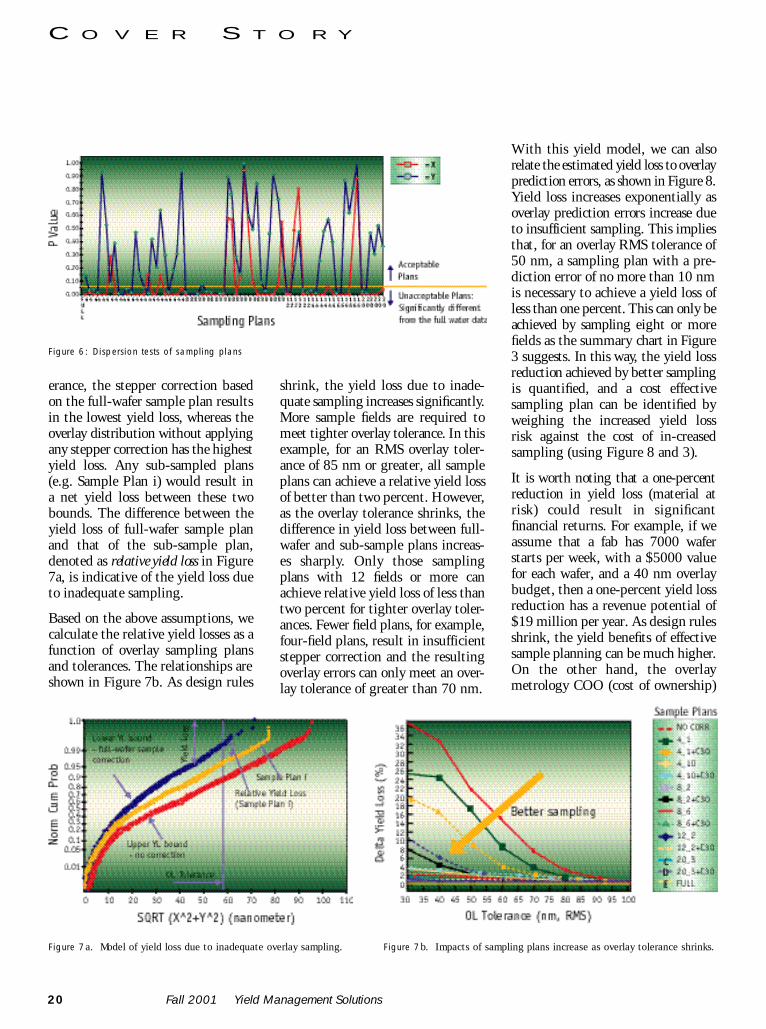


![Å®» »Y¼ ÆL»Y»Y¼£¿Û ½@» ºdb.cs.duke.edu/courses/cps216/fall01/papers/haas-sigmod... · 1999-04-18 · =Z ^] \ _ \ _ ^] \ _ \.? -¿ = ¯ ~)¶ · > °](https://static.documents.pub/doc/80x56/5f495d40edf3136ebf221413/-y-lyy-dbcsdukeeducoursescps216fall01papershaas-sigmod.jpg)


![[PPT]PowerPoint Presentation - Rowan University - Personal …users.rowan.edu/.../fall01/comparch2/lectures/Compiler.ppt · Web viewA 1 Example Process to construct a Pushdown Machine](https://static.documents.pub/doc/80x56/5aa21ccb7f8b9ac67a8caf8f/pptpowerpoint-presentation-rowan-university-personal-usersrowanedufall01comparch2lectures.jpg)


