Page 1
Emergence of a weak topological insulator from the BixSey
family and the observation of weak anti-localization
Kunjalata Majhi†1, Koushik Pal†2, Himanshu Lohani3, Abhishek Banerjee1,
Pramita Mishra3, Anil K Yadav1,4, R Ganesan1, BR Sekhar3, Umesh V
Waghmare2, and PS Anil Kumar1,5
1Indian Institute of Science, Bangalore-560012, India
2Theoretical Sciences Unit, Jawaharlal Nehru Centre for Advanced Scientific
Research, Bangalore-560064, India
3Institute of Physics, Bhubaneshwar-751005, India
4Department of Physics, Ch. Charan Singh University, Meerut-250004, India
5Center for Nano Science And Engineering, Bangalore-560012, India
May 6, 2016
†These authors have equally contributed to this work.
arX
iv:1
605.
0161
3v1
[co
nd-m
at.m
trl-
sci]
5 M
ay 2
016
Page 2
Abstract
The discovery of strong topological insulators led to enormous activity in condensed matter
physics and the discovery of new types of topological materials. Bisumth based chalcogenides
are exemplary strong three dimensional topological insulators that host an odd number of
massless Dirac fermionic states on all surfaces. A departure from this notion is the idea of a
weak topological insulator, wherein only certain surface terminations host surface states char-
acterized by an even number of Dirac cones leading to exciting new physics. Experimentally
however, weak topological insulators have proven to be elusive. Here, we report a discovery
of a weak topological insulator (WTI), BiSe, of the Bi-chalcogenide family with an indirect
band gap of 42 meV. Its structural unit consists of bismuth bilayer (Bi2), a known quantum
spin hall insulator sandwiched between two units of Bi2Se3 which are three dimensional strong
topological insulators. Angle resolved photo-emission spectroscopy (ARPES) measurements on
cleaved single crystal flakes along with density fucntional theory (DFT) calculations confirm
the existence of weak topological insulating state of BiSe. Additionally, we have carried out
magneto-transport measurements on single crystal flakes as well as thin films of BiSe, which
exhibit clear signatures of weak anti-localization at low temperatures, consistent with the prop-
erties of topological insulators.
Page 3
0.1 Introduction
The discovery of topological insulators(TIs) is one of the recent breakthroughs in condensed
matter physics. They have been at the forefront of materials research due to their unique elec-
tronic properties and potential for wide range of applications. Like band insulators, TIs host
a bulk band gap and do not conduct electricity in the bulk. However, on the surface they host
robust symmetry protected massless metallic states that support spin-polarized conduction1–3.
These surface states result from the bulk electronic topology and associated band inversion due
to strong spin-orbit coupling. The low energy dynamics of such massless surface states can be
described with a Dirac Hamiltonian with spin locked to momentum H=~vF (σ×k).z, where ~ is
reduced Plank’s constant, vF is the fermi velocity, σ stands for Pauli matrices and k is the wave
vector. The topology of a time-reversal (TR) symmetry invariant insulator is characterized by
Z2 indices which can be either be zero (topologically trivial) or one (topologically non-trivial)4,5.
In 2-D, a single Z2 invariant (ν0) specifies the topology, where as in 3-D four Z2 invariants are
needed (ν0,ν1,ν2,ν3)6,7. In 3-D, a TR invariant topological insulator can further be classified as
strong topological insulator (STI)8–10 or weak topological insulator (WTI), based on whether
a TI hosts odd or even number of Dirac cones on its surfaces respectively. For an STI, ν0=1
and (ν1,ν2,ν3) can be 0 or 1, whereas for a WTI, ν0=0 and atleast one of (ν1,ν2,ν3) should be
non-zero4–7,11. While an STI exhibits topological surface states (TSS) with odd number of Dirac
cones on any surface8–10, a WTI hosts TSS with even number of Dirac cones only at specific
surface planes12. A WTI phase can be adiabatically connected to stacked layers of 2D strong
TIs12,13, and its surface states are linked to the edge states of each 2D TI layer. Translational-
invariant coupling between these layers gaps out the surface states perpendicular to the layer
directions14, leaving the Dirac cones to manifest only at their side surfaces12,15,16. In this regard,
TSSs in STI are always manifested whereas they are either manifested or hidden in case of a
WTI12,17,18.
The surface states of WTI were initially thought to be unstable towards non-magnetic disor-
der7,17–21 . However, it has been shown recently that WTI surface states are robust against
strong TR-invariant disorder16,18, similar to those of STIs. These states are further predicted to
exhibit intriguing quantum phenomena such as one-dimensional helical modes along dislocation
lines19,20, weak-anti-localization (WAL) effect16, half quantum spin hall effect22. Additionally,
WTIs offer new possibilities to obtain 2D TIs by exfoliating a single quantum spin hall (QSH)
layer from the bulk which is technically more feasible than fabricating complicated quantum
1
Page 4
wells23,24. However, the WTI phase has been proved to be elusive experimentally. KHgSb25,
Bi2TeI26 and a superlattice structure of PbTe/SnTe27 are theoretically proposed to be WTIs,
but their experimental verifications is yet to be achieved. The bismuth-based layered compound
Bi14Rh3I913,28 is the only known experimental realization of a WTI. The intuitive design of a
WTI material borrows from an idea that a stack of weakly coupled 2D topological insulators
may lead to a 3D WTI. For example, Bi14Rh3I9 is essentially a stacked graphene analogue13,
with each layer exhibiting a large spin orbit interaction at bismuth. Another promising route is
to stack alternating bismuth bilayers (2D topological insulator) with a trivial insulator. Bi2TeI
follows this paradigm and has been theoretically shown to be a WTI, but with no experimen-
tal verification. Primarily, the difficulty in fabrication of these materials in single crystalline
bulk or thin film form has proven to be a significant hindrance to research in weak topological
insulators.
In this letter, we present possibly the simplest realization of a weak topological insulator,
borrowing essentially from two observations. First, bismuth bilayers are exemplary quantum
spin hall insulators29–32 . Therefore a stack of coupled Bi2 bilayers should ideally give rise
to a 3D WTI. We intuit that stacking of bismuth bilayers sandwiched on either side by a
topological insulator instead of a trivial insulator could also possibly host a WTI. Second,
and more importantly, it is known that the bismuth chalcogenides exhibit what is known as
‘infinitely adaptive superlattice’ phase33. The stoichiometry of BixSey can be adjusted to a wide
range of values by composing stacks of Bi2Se3 and Bi2 with thickness of suitable ratio. For the
simplest possible ratio with x = 1 and y = 1, one obtains a crystal structure as shown in Fig.
1a wherein a repeating unit is formed by a Bi2 bilayer sandwiched bwtween two Bi2Se3 layers.
The hallmark of this structure is that it consists of quantum spin hall insulators29,34,35 that are
coupled to each other through 3D topological insulators4,5, 7, 8.
With combined experimental and theoretical studies, we show that BiSe belongs to (0;001)
class of Z2 weak TIs, where the band inversion takes place at Γ and A points in the Bril-
louin Zone, which is contributed by both the Bi2 layer and Bi2Se3 quintuple layers. To probe
surface transport properties, we grow thin films of BiSe and study magnetotransport at low
temperatures. Magnetoresistance measurements indicate a pronounced weak-antilocalization
cusp, consistent with a strong spin-orbit coupling in the system.
2
Page 5
Theoretical Analysis
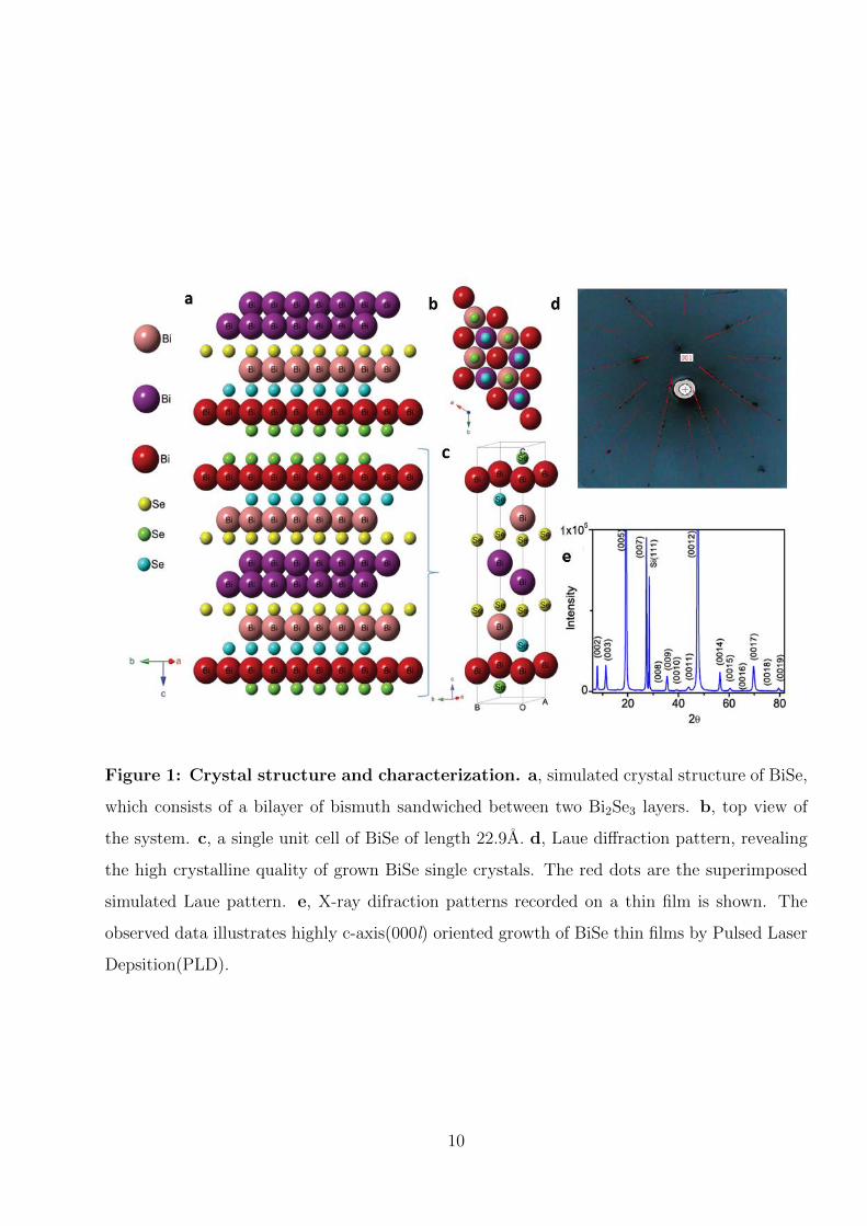
Electronic structure of BiSe, calculated within a non-relativistic approximation at the experi-
mental lattice constant36 (see Fig. 2), reveals a metallic character with a flat conduction band
along Γ-A line just above Fermi level (EF ), which is highly localized and confined to the bis-
muth bilayer (see Supplementary Fig. S 1b). Dispersion of this band near the EF (along Γ-A)
is similar to that of an unconventional superconductor MgB237 and weak topological insulators
like Bi2TeI26 and KHgSb25. This unoccupied conduction band is constituted primarily of σ-
bonded px and py orbitals of Bi in the bismuth bilayer, and becomes dispersion-less due to weak
interlayer interaction. Such empty covalent bonds cost energy, and this flat band pushes BiSe
to the brink of lattice instability (with imaginary frequency of ∼ i15 cm−1 appearing along Γ-A
direction, the crystallographic direction of stacking in BiSe, see Fig. 2d). Orbital projected
electronic structure reveals that the contributions to the valence band (VB) and conduction
band (CB) around the Fermi level are mainly from the Bi bilayer and Bi2Se3 quintuple layers
(QLs) respectively, except along the Γ-A line where this is reversed, indicating the inverted
band structure and existence of topologically nontrivial phase in BiSe. With inclusion of spin-
orbit coupling in determination of electronic structure ( see Fig. 2b), the doubly degenerate
flat bands split opening up a gap along Γ-A, and elsewhere in the Brillouin Zone (smallest
indirect gap being 42 meV). As BiSe is centrosymmetric and invariant under time reversal, the
topological Z2 invariant of its electronic structure effectively determines its topological nature.
We determine the four Z2 invariants (ν0; ν1, ν2, ν3) from the parity of occupied bands at eight
time reversal invariant momenta (TRIM) following Fu and Kane’s work7. The strong topolog-
ical index, ν0, is calculated by taking the product of the parity of occupied bands (σi) at eight
TRIM through the relation (−1)ν0 =∏8
i=1 σi, where i runs over eight TRIM, and σi =∏
m ξ2m,
ξ being the parity of the 2mth occupied band at i-th TRIM. The other three weak topological
indices (νk, k = 1, 2, 3) are determined using (−1)νk =∏4
i=1 σi, where i runs over the four
TRIMs (see Supplementary Section IV for detailed analysis). The Z2 invariants of BiSe are
(0;001), showing that it belongs to a class of weak topological insulators like KHgSb25 and
Bi2TeI26.
Goverts et al.38 recently questioned the claim that bismuth bilayer terminated Bi2Se3 ex-
hibits a single Dirac cone in the electronic structure of (001) surface39 . They showed that
the Dirac-like cone in Bi2 terminated surface actually corresponds to Rashba split states of
the bismuth bilayer which arises from the presence of an internal electric filed associated with
3
Page 6
polarity and charge transfer from Bi2 to Bi2Se3 quintuple layers38. Our results for the electronic
structure of (001) surfaces with different surface terminations and thicknesses of BiSe indeed
agree with Goverts et al.38 . Thus, the composite system BiSe neither possesses the strong
topological properties of Bi2Se38 nor of Bi2 layers40 (see Supplementary Section V). To further
confirm the weak topological nature of BiSe, we determined surface electronic structure on
(100) surface (i.e. yz-plane of the unit cell, see Supplementary Section I and Fig. S 3c,d) of
BiSe, which reveals two(even number of) Dirac cones at Y and T points of the Brillouin zone
(see Fig. 2c). Similar to the case of another weak TI, Bi2TeI26, the two Dirac points (Y and
T ) are not the projections of Γ and A points of the bulk on the (100) plane of the reciprocal
space in Fig. S 3d.
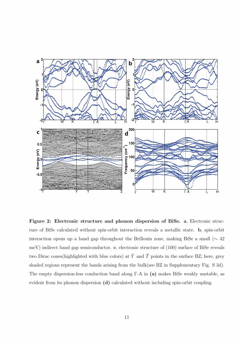
Angle Resolved Photoemission Spectroscopy
Angle-resolved photo-emission spectroscopy (ARPES) measurements were carried out on a thin
single crystalline flake of BiSe cleaved in situ under a base pressure of 1x10⁻¹⁰ mbar. In the
ARPES spectrum of BiSe along the Γ-M direction of the surface Brillouin zone (see Fig. 3a),
the high intensity signal around binding energy (BE) Eb=-0.25 eV corresponds to the bulk
valence band (BVB) states, whereas the bulk conduction band (BCB) states are close to fermi
energy EF (Eb ' −0.03eV ). Interestingly, we find two states in the region between the BCB
and BVB showing inverted parabolic dispersion (marked with green dots). These states are
marked as surface state bands (SSB), prototypical of Rashba spin-split (RSS) states. The apex
of these Rashba Split (RS) states barely touches the EF around K||=± 0.20 A−1 (denoted as
k0). Crossing of these bands (ER) occurs at Eb ∼ -0.18 eV at the Γ-point. In the vicinity of
this point, these bands exhibit nearly linear dispersion, like Dirac cone states. However, ER is
not clearly visible due to mixing of this feature with the BVB states. The Rashba parameter
2ER/k0 which has been calculated by using the estimated values of ER and k0 from the ARPES
data (see Fig. 3a) is 1.8 eVA. Comparing these results with the relativistic band structure of
BiSe (see Fig. 2b) along the (001) plane, it is clear that the calculated surface states, appearing
along the Γ-M direction (marked by red color box) due to strong spin-orbit coupling (SOC),
are in fairly good agreement with the SSB observed in the ARPES image. However, the energy
position of the SSB in the calculated band structure is at a lower binding energy than that in
the experimental ARPES data. This difference in the energy position could be due to band
4
Page 7
bending41 and/or due to intrinsic doping from charged defects.
In order to understand the isotropic nature of the SSB, we measured the ARPES spectra
along two different orientation: ∼ 80 (Γ-M′) and ∼ 150 (Γ-M”) offset from the Γ-M direction.
Along the Γ-M′
direction, the second RS state is completely visible(see Fig. 3c), unlike the
previous case (see Fig. 3a). However, the separation between the two RS states is not well
resolved and a dumbbell shape intensity distribution is observed around the Γ- point. In the
other k-direction Γ-M”, maximum of the second parabolic band appears blurred and near the
EF intensity distribution shows a pear shape structure around the Γ-point, as seen in Fig. 3d. It
is clear from these ARPES images that there are two Rashba spin split SSB states in BiSe which
arise from the Rashba splitting of states in the Bi bilayer due to potential gradient generated
from the charge transfer from Bi bilayer to the Bi2Se3 quintuple layers. Though, the RS states
like SSB are not well resolved, these observations are close to our theoretical band-structure
prediction of weak topologically insulating phase in BiSe. Secondly, these observations are also
consistent with a previous ARPES study on a similar system i.e. Bi films grown on Bi2Se342.
On the other hand, these SSB are remarkably different from the SSB found in a typical strong
topological insulator, for example Bi2Se3, shown in Fig. 3e. In this case, the single Dirac
cone like feature is clearly visible in the vicinity of EF near the Γ-point. This difference in the
observed ARPES intensity pattern between BiSe and strong TI, Bi2Se3 further confirms the
topologically distinct character of the SSB in BiSe.
Low temperature magnetotransport measurements
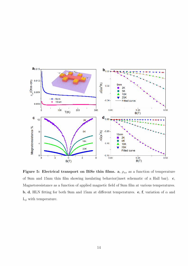
The electronic structure of BiSe has its signatures in the low temperature magneto-transport
properties (see Fig. 4a). We find that its resistivity increases with temperature, marking a
metallic behavior. The carrier concentration and mobility estimated from Hall effect mea-
surement are ne = 5.14 × 1020cm−3 and µ = 722cm2V −1s−1 respectively for a single crystal
flake of thickness 0.22mm. This carrier concentration can be attributed to selenium vacancy
defects as corroborated by our ARPES measurements, but a large bulk carrier concentration
proves to be a major obstacle in sieving out transport properties of only the surface states.
Resistance measured in a perpendicular magnetic field (see Fig. 4b) produced non-saturating
linear magnetoresistance. Though, the origin of linear magnetoresistance is highly debated, we
assume this might be due to the continously varrying fluctuations in the conductivity in the
5
Page 8
weak disorder limit43(discussed later).
A large bulk conduction observed in single crystal flakes of thickness of the order of mil-
limeters can be quantified with dimensional scaling of properties of films. Hence, we grew thin
crystalline films of BiSe using pulsed laser deposition(PLD) on SiO2(500nm)/Si(111) substrates.
We used X-ray diffraction and atomic-force microscopy to characterize the crystallinity of our
thin films and determine the surface morphology respectively (see Supplementary section I).
Electrical transport measurements were carried out on two BiSe films patterned into standard
six probe Hall bars of different thickness, both in the ultra-thin regime. In the zero-field resis-
tivity ρxx data for 9nm and 15nm samples as a function of temperature (see Fig. 5a), a sharp
low-temperature resistivity upturn below ∼30K is indicative of an insulating ground state at
low temperatures. At T=230K, we observe another transition from metallic to semiconducting
state. This can be explained as follows: in the two channel model with a metallic surface
in parallel with a semiconducting bulk44, the net conductance of the sample is dominated by
the more conducting channel. As a function of increasing temperature, the conductance of
the metallic channel decreases linearly while that of the semiconducting bulk increases ex-
ponentially. One therefore expects a cross-over temperature above which conductance of the
semiconducting bulk exceeds the conductance of the metallic surface states originating from
the Rashba-spin split bands, driving a high temperature transition to semiconducting behav-
ior. This is what we observe for the 15nm film. However, for the 9nm film, where the bulk
conduction is smaller, such a transition is expected to happen at a higher temperature, and we
therefore do not observe it in our measurements till 300K. We observed linear Hall resistance
for both 15nm and 9nm samples. The linearity indicates that majority of charge cariers are
of simillar type and mobility45. The carrier concentrations of both the samples are of the same
order with ne = 9.3 × 1019cm−3 for 15 nm sample and ne = 4.7 × 1019cm−3 for 9 nm sample.
Mobility of the samples is low: with µ = 10cm2V −1s−1. Such low mobilites indicate strong
scattering from static disorder present in the sample. Assuming a spherical Fermi surface,46
we estimated γ = 1πkf l
, where γ is a dimensionless parameter that measures the strength of
disorder, kf is fermi wave vector and l is the mean free path, to be 0.25 and 0.40 for 15nm
and 9nm respectively (γ � 1, corresponds to weak disorder), which indicates that our films
fall in the weak-disorder regime. In the limit of weak disorder, weak localization corrections to
conductivity are expected to appear at low temperatures. By applying a small magnetic field,
the weak localization correction to conductivity can be destroyed thereby forming a powerful
6
Page 9
tool to probe weakly disordered conductors. A wealth of information about electron dynam-
ics including phase relaxation lifetimes, nature of disorder and symmetry classes of governing
Hamiltonians can be extracted from these measurements.
Since, 3D topological insulators (both STIs and WTIs) belong to the symplectic class in
Altland-Zirnbauer classification47 , they exhibit weak anti-localization, with correction to the
Drude conductivity arising from destructive interference of time-reversed paths. With applica-
tion of magnetic field, time reversed trajectories accumulate opposite phases, eventually leading
to decoherence when the phase difference is of order ∼ π. This magnetic field induces suppres-
sion of weak anti-localization corrections in two dimensional systems is quantified by the HLN
equation48, ∆GWAL(B) = ∆Gxx(B) − ∆Gxx(0) = α e2
2π2~ [ln( ~4BeL2
φ) − Ψ(1
2+ ~
4BeL2φ)], where e
is charge of electron, Lφ is the phase coherence length, α is WAL co-efficient and Ψ is the
digamma function.
We measured magneto-resistance at different temperatures from 2K to 25K in a perpendic-
ular B-field upto 7T (see Fig. 5b). At low temeperatures, in contrast to single crystal flake,
a well-defined weak-anti-localization cusp is clearly seen in the low field region that graduates
into a linear magnetoresistance regime for higher fields. Fitting the HLN equation upto 0.5T,
we find out the phase coherence LΦ (45nm, 73nm at 2K) and α (0.33, 0.42 at 2K) for 9nm
and 15nm films respectively (see Fig. 5b and 5d). From WAL point of view, α corresponds
to the number of 2D coherent conduction channels present in the system. A coherent channel
having a π-Berry’s phase should contribute a value of 0.5 to α. We observed that the value of
α remains close to 0.5 (0.33 and 0.42 for 9m and 15nm respectively) indiacting a single coher-
ent conducting channel contributing to the conductance. The phase-coherence length increases
moderately from 45nm to 73nm with thickness. It is interesting to note that parallel field yeilds
significantly lower magnetoresistance compared to perpendicular field configuration simillar to
STIs (see Supplementary section II), which needs to be understood further.
The observed WAL is a result of destructive intereference of electron paths due to π Berry’s
phase in topological insulators. The appearance of WAL in our system indicates the pres-
ence of topologically protected surface states, also unlike topologically trvial systems it doesn’t
exhibit any cross-over from WAL to WL49 . Spin orbit coupling of the Rashba type leads to
chiral fermions with spin locked perpendicular to the direction of momentum. Such states con-
tribute to quantum transport through weak anti-localization and have been observed in several
other systems50. Functionalization and control of such states is highly desired, and has received
7
Page 10
tremendous recent attention as they form building blocks of next generation electronic technolo-
gies like Majorana-fermion based quantum computing and spintronics. Transport properties
of WTIs may offer exciting new opportunities in these directions, apart from forming a fertile
ground for investigating new topological physics.
Conclusion
Weak topological insulators are relatively rare phases of topological matter. While a wealth
of information about this phase is available from theoretical analysis, a thorough experimental
verification and understanding have been lacking. We demonstrate that BiSe, belonging to
the richly explored bismuth chalcogenide family, is a weak topological insulator. With first-
principles calculations, we reveal that BiSe exhibits a pair of band inversions at Γ andA points in
the 3D Brillouin Zone, and calculation of the four Z2 topological indices confirm the WTI phase.
Strikingly, we find that bismuth bilayer terminated (001) surface reveals gap-less Rashba spin
split states. ARPES measurements on single crystals cleaved in the (001) direction provide clear
indications of surface states showing Rashba spin splitting, and other features of the spectra
match closely with the calculated electronic sturcture. To investigate the ‘weakness’ of a WTI,
we perform electronic transport measurements on BiSe thin films that reveal signatures of weak
anti-localization. Thus, we provide a simple route towards fabrication of a WTI amenable to
exfoliations and point out the experimental signatures of this 3D topological phase, that will
guide developement of other WTI’s.
Ackowledgement
KM thanks CSIR India for the financial support. PSAK thanks Nanomission, DST, India for
financial support. UVW thanks DST, India for support through a JC Bose National fellowship.
Methods
Sample preparation and transport measurement
Single crystals of BiSe have been grown by modified Bridgman method and characterized by
Laue method shows good crystalline quality. Thin films of BiSe have been prepared by Pulsed
8
Page 11
Laser Deposition with laser source of wavelength 248nm and energy 31mJ. To study transport
properties we preferred to grow BiSe on Si(111) with SiO2(500nm) substrates to avoid any kind
of substrate contribution to the sample as the resistivity of the samples are very high. Standard
six-probe hall bar shaped thin films were prepared by shadow masking for transport measure-
ments. For electrical contacts, Cr/Au (10nm/65nm) were deposited by thermal evaporation
method. The samples were wire-bonded (Al wire) to a PCB. All the transport measurements
are carried out in an Oxford 2K system at a magnetic field up to B=7T.
ARPES measurement
ARPES spectra were collected using a high flux GAMMADATA VUV He-I (21.2eV) source
and SCIENTA R3000 analyzer. At the HeI line (21.2 eV), the photon flux is of the order of
1016 photons/s/steradian with a beam spot of 2mm. Fermi energies were calibrated by using
a freshly evaporated Ag film on the sample holder. The total energy resolution estimated from
the width of the Fermi edge, was about 27 meV for HeI excitation energy while the angular
resolution better than 1A in the wide-angle mode (8A) of the analyser.
9
Page 12
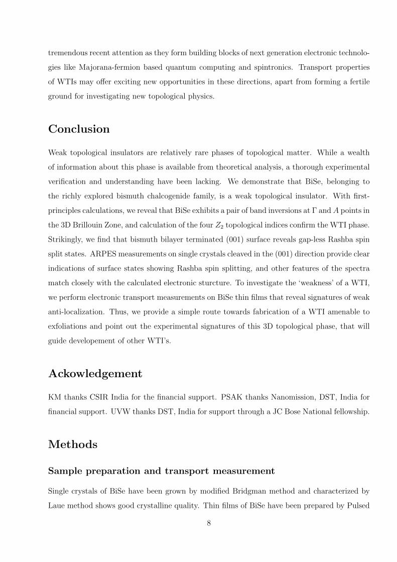
Figure 1: Crystal structure and characterization. a, simulated crystal structure of BiSe,
which consists of a bilayer of bismuth sandwiched between two Bi2Se3 layers. b, top view of
the system. c, a single unit cell of BiSe of length 22.9A. d, Laue diffraction pattern, revealing
the high crystalline quality of grown BiSe single crystals. The red dots are the superimposed
simulated Laue pattern. e, X-ray difraction patterns recorded on a thin film is shown. The
observed data illustrates highly c-axis(000l) oriented growth of BiSe thin films by Pulsed Laser
Depsition(PLD).
10
Page 13
Y T ZΓ
a b
c d
Figure 2: Electronic structure and phonon dispersion of BiSe. a, Electronic struc-
ture of BiSe calculated without spin-orbit interaction reveals a metallic state. b, spin-orbit
interaction opens up a band gap throughout the Brillouin zone, making BiSe a small (∼ 42
meV) indirect band gap semiconductor. c, electronic structure of (100) surface of BiSe reveals
two Dirac cones(highlighted with blue colors) at Y and T points in the surface BZ; here, grey
shaded regions represent the bands arising from the bulk(see BZ in Supplementary Fig. S 3d).
The empty dispersion-less conduction band along Γ-A in (a) makes BiSe weakly unstable, as
evident from its phonon dispersion (d) calculated without including spin-orbit coupling.
11
Page 14
Figure 3: Angle-resolved photoemission spectroscopy on BiSe. a, the ARPES spec-
trum along the Γ-M direction of the surface Brillouin zone of the BiSe. Surface state band (SSB),
bulk valence band (BVB) and conduction band (BCB) are marked. b, relativistic surface elec-
tronic structure of bismuth bilayer terminated BiSe calculated on (001) plane. Red color box
encloses Rashba spin split (RSS) states, where Dirac-like linear dispersing is highlighted with
cyan color. c, d, show ARPES intensity plots taken along Γ-M′
and Γ-M” directions which are
80 and 150 away from the perfect Γ-M direction respectively. Difference in the energy position
of crossing of RS like bands(ER) between (a) and (d) could be possibly a clear signature of
band bending effect because ARPES spectra was taken after half an hour from the cleaving
while later case it was collected after four hour from the cleaving. e, displays ARPES intensity
plot of Bi2Se3 along the Γ-M direction. The bulk and surface states are clearly distinguished
and Dirac point (DP) occurs around binding energy Eb = -0.28 eV.
12
Page 15
Figure 4: Electrical transport measurement on BiSe single crystal. a, ρxx as a
function of temperature shows linear behavior with temperature of a single crystal flake of
thickness 0.22mm and b, shows linear magnetoresistance as a function of magnetic field at
different temperatures.
13
Page 16
Figure 5: Electrical transport on BiSe thin films. a, ρxx as a function of temperature
of 9nm and 15nm thin film showing insulating behavior(inset schematic of a Hall bar). c,
Magnetoresistance as a function of applied magnetic field of 9nm film at various temperatures.
b, d, HLN fitting for both 9nm and 15nm at different temperatures. e, f, variation of α and
Lφ with temperature.
14
Page 17
Bibliography
1 Moore, Joel E. The birth of topological insulators. Nature 464, 194 (2010).
2 Qi, Xiao-Liang. & Zhang, Shou-Cheng. Topological insulators and superconductors. Rev. Mod.
Phys. 83, 1057–1110 (2011).
3 Hasan, M. Z. & Kane, C. L. Colloquium : Topological insulators. Rev. Mod. Phys. 82, 3045–
3067 (2010).
4 Fu, Liang. Kane, C. L. & Mele, E. J. Topological Insulators in Three Dimensions. Phys. Rev.
Lett. 98, 106803 (2007).
5 Moore, J. E. & Balents, L. Topological invariants of time-reversal-invariant band structures.
Phys. Rev. B 75, 121306 (2007).
6 Roy, Rahul. Topological phases and the quantum spin Hall effect in three dimensions. Phys.
Rev. B 79, 195322 (2009).
7 Fu, Liang. & Kane, C. L. Topological insulators with inversion symmetry. Phys. Rev. B 76,
045302 (2007).
8 Zhang, H. et al. Topological insulators in Bi2Se3, Bi2Te3 and Sb2Te3 with a single Dirac cone
on the surface. Nature Physics 5, 438-442 (2009).
9 Xia, Y. et al. Observation of a large-gap topological-insulator class with a single Dirac cone
on the surface. Nature Physics 5, 398-402 (2009).
10 Chen, Y. L. et al. Experimental Realization of a Three-Dimensional Topological Insulator,
Bi2Te3. Science 325, 178–181 (2009).
11 Kane, C. L. & Mele, E. J. Z2 Topological Order and the Quantum Spin Hall Effect. Phys.
Rev. Lett. 95, 146802 (2005).
15
Page 18
12 Ringel, Zohar., Kraus, Yaacov E. & Stern, Ady. Strong side of weak topological insulators.
Phys. Rev. B 86, 045102 (2012).
13 Rasche, Bertold. et al. Stacked topological insulator built from bismuth-based graphene sheet
analogues. Nat. Matt. 12, 422 (2013).
14 Obuse, Hideaki., Ryu, Shinsei., Furusaki, Akira. & Mudry, Christopher. Spin-directed net-
work model for the surface states of weak three-dimensional Z2 topological insulators Phys.
Rev. B 89, 155315 (2014).
15 Arita, Takashi. & Takane, Yositake. Effective Model for Massless Dirac Electrons on a Surface
of Weak Topological Insulators Journal of the Physical Society of Japan, 83 (2012)no 12.
16 Mong, Roger S. K., Bardarson, Jens H. & Moore, Joel E. Quantum Transport and Two-
Parameter Scaling at the Surface of a Weak Topological Insulator. Phys. Rev. Lett. 108,
076804 (2012).
17 Imura, Ken-Ichiro., Takane, Yositake. & Tanaka, Akihiro. Weak topological insulator with
protected gapless helical states. Phys. Rev. B 84, 035443 (2011).
18 Morimoto, Takahiro. & Furusaki, Akira. Stability of surface states of weak Z2 topological
insulators and superconductors. Phys. Rev. B 89, 035117 (2014).
19 Ran, Ying., Zhang, Yi. & Vishwanath, Ashvin. One-dimensional topologically protected
modes in topological insulators with lattice dislocations. Nat. Phys. 5, 298-303 (2009).
20 Yoshimura, Yukinori., Matsumoto, Akihiko. & Takane, Yositake. & Imura, Ken-Ichiro. Per-
fectly conducting channel on the dark surface of weak topological insulators. Phys. Rev. B
88, 045408 (2013).
21 Nomura, Kentaro., Koshino, Mikito. & Ryu, Shinse. Topological Delocalization of Two-
Dimensional Massless Dirac Fermions. Phys. Rev. Lett. 99, 146806 (2007).
22 Liu, Chao-Xing., Qi, Xiao-Liang. & Zhang, Shou-Cheng. Half quantum spin Hall effect on
the surface of weak topological insulators. Physica E: Low-dimensional Systems and Nanos-
tructures 44, 906 - 911 (2012).
23 Bernevig, B.A., Hughes, T.L. & Zhang, S.C. Quantum spin Hall effect and topological phase
transition in HgTe quantum wells. Science 314 (5806), 1757-1761 (2006).
16
Page 19
24 Konig, Markus. et al. Quantum Spin Hall Insulator State in HgTe Quantum Wells. Science
318, 766-770 (2007).
25 Yan, Binghai., Muchler, Lukas. & Felser, Claudia. Prediction of Weak Topological Insulators
in Layered Semiconductors. Phys. Rev. Lett. 109, 116406 (2012).
26 Tang, Peizhe. et al. Weak topological insulators induced by the interlayer coupling: A first-
principles study of stacked Bi2TeI. Phys. Rev. B 89, 041409 (2014).
27 Yang, G., Liu, J., Fu, L., Duan, W. & Liu, C. Weak topological insulators in PbTe/SnTe
superlattices. Phys. Rev. B 89, 085312 (2014).
28 Pauly, Christian. et al.Electronic Structure of the Dark Surface of the Weak Topological
Insulator Bi14Rh3I9. ACS Nano 10.1021/acsnano.6b00841 (2016).
29 Murakami, Shuichi. Quantum Spin Hall Effect and Enhanced Magnetic Response by Spin-
Orbit Couplings. Phys. Rev. Lett. 97, 236805 (2006).
30 Jin, Kyung-Hwan. & Jhi, Seung-Hoon. Quantum anomalous Hall and quantum spin-Hall
phases in flattened Bi and Sb bilayers. Scientific Reports 5, 8426 (2015)
31 Liangzhi, Kou. et al. Tetragonal bismuth bilayer: a stable and robust quantum spin hall
insulator. 2D Materials 4, 045010 (2015)
32 Drozdov, Ilya K. et al. One-dimensional topological edge states of bismuth bilayers. Nat Phys
10, 664-669 (2014).
33 Valla, T. et al. Topological semimetal in a Bi-Bi2Se3 infinitely adaptive superlatice phase
Phys. Rev. B 86, 241101 (2012).
34 Yang, Fang. et al. Spatial and Energy Distribution of Topological Edge States in Single
Bi(111) Bilayer. Phys. Rev. Lett. 109, 016801 (2012).
35 Liu, Zheng. et al. Stable Nontrivial Z2 Topology in Ultrathin Bi (111) Films: A First-
Principles Study. Phys. Rev. Lett. 107, 136805 (2011).
36 Gaudin, E., Jobic, S., Evain, M., Brec, R. & Rouxel, J. Charge balance in some BixSey phases
through atomic structure determination and band structure calculations. Materials Research
Bulletin 30, 549-561 (1995).
17
Page 20
37 Choi, H. J., Roundry, D., Sun, H., Cohen, M. L. & Louie, S. G. The origin of the anomalous
superconducting properties of MgB2. Nature 418, 758-760 (2002).
38 Goverts, K., Park, K., De Beule, C., Partoens, B. & Lamoen, D. Effect of Bi bilayers on the
topological states of Bi2Se3: A first-principles study. Phys. Rev. B 90, 155124 (2014).
39 He, X. et al. Surface termination of cleaved Bi2Se3 investigated by low energy ion scattering.
Phys. Rev. Lett. 110, 156101 (2013)
40 Wada, M., Murakami, S., Freimuth, F. & Bihlmayer, G. Localized edge states in two-
dimensional topological insulators: Ultrathin Bi films. Phys. Rev. B 83, 121310(R) (2011).
41 Ishizaka, K. et al. Giant Rashba-type spin splitting in bulk BiTeI. Nat. Matt. 10, 521 (2011).
42 Miao, Lin. et al. Quasiparticle dynamics in reshaped helical Dirac cone of topological insula-
tors. PNAS 110, 2758 (2013).
43 Parish, M. M. & Littlewood, P. B. Non-saturating magnetoresistance in heavily disordered
semiconductors. Nature 426, 162 (2003).
44 Pan, Y. et. al. Low carrier concentration crystals of the topological insulator Bi2-xSbxTe3-
ySey: a magnetotransport study. New journal of physics 16, 123035 (2015).
45 Bansal, Namrata.et al. Thickness-Independent Transport Channels in Topological Insulator
Bi2Se3 Thin Films. Phys. Rev. Lett. 109, 116804 (2012).
46 Vollhardt, Dieter. Localization Effects in Disordered Systems Adnavances in Solid State
Physics. 27, 63-84 (2007).
47 Altland, Alexander. & Zirnbauer, Martin R. Nonstandard symmetry classes in mesoscopic
normal-superconducting hybrid structures. Phys. Rev. B 55, 1142–1161 (1997).
48 Hikami, Shinobu., Anatoly I. Larkin & Nagaoka, Yosuke. Spin-orbit interaction and mag-
netoresistance in the two dimensional random system. Progress of Theoretical Physics 63.2,
707-710 (1980).
49 Liu, M. et. al. Crossover between Weak Antilocalization and Weak Localization in a Mag-
netically Doped Topological Insulator. Phys. Rev. Lett. 108, 036805 (2012).
18
Page 21
50 Koga, T., Nitta, J., Akazaki, T. & Takayanagi, H. Rashba Spin-Orbit Coupling Probed by
the Weak Antilocalization Analysis in InAlAs/InGaAs/InAlAs Quantum Wells as a Function
of Quantum Well Asymmetry. Phys. Rev. Lett. 89, 046801 (2002).
19