i
Feasibility Study of Using PDMS as an Alternate Transmittance Cell Kit in an FTIR
Spectrometer
Harish Krishnan
A Thesis
In
The Department
of
Mechanical and Industrial Engineering
Presented in Partial Fulfillment of the Requirements
For the Degree of Master of Applied Science (Mechanical Engineering) at
Concordia University
Montreal, Quebec, Canada
April 2012
©Harish Krishnan, 2012
iii
ABSTRACT
Feasibility Study of Using PDMS as an Alternate Transmittance Cell Kit in an FTIR
Spectrometer
Harish Krishnan
Polydimethylsiloxane (PDMS) based microdevices have bought revolutionary change in
the chemical analysis. Suitable mechanical properties of PDMS make it amenable for soft
lithography and certain optical properties like transparency in Near InfraRed (NIR) make
it a yet unexplored option for use as a window material in Fourier Transform InfraRed
(FTIR) Spectrometers. In our work, we investigate the utility of PDMS as a transmittance
cell kit in FTIR Spectrometer replacing the CaF2 windows that are currently in use.
In this work, the spectral characteristics of PDMS in NIR and MIR have been thoroughly
investigated. A set of design parameters were extracted through experiments and a
preliminary design for a PDMS based cell kit has been suggested. PDMS Cell kit was
fabricated using a SU-8 coated silicon wafer mold using soft lithography. Experiments by
varying the base to curing agent ratio of PDMS pre polymer as well as selected heat
treatment protocols were conducted, to improve the transmittance of PDMS in the MIR
region. Due to the variation in base transmittances of PDMS across different samples and
also due to inherent variations introduced by the FTIR spectrometer, there has not been
an appreciable change in the optical characteristics of PDMS.
Further, to prove the utility of PDMS as a window material in the NIR region, Samples of
Extra Virgin Olive Oil (EVOO) were analyzed with the PDMS cell kit and the results
iv
were compared with the spectral analysis on same samples with a CaF2 kit. Even though
PDMS does introduce its own artifacts, if a critical sample volume is used for the
analysis, the performance of the PDMS kit is comparable to that of CaF2 cell kit. This
volume which is dependent on the ratio of the thickness of a particular sample to that of
the PDMS slabs, and the Critical Volume Ratio (CVR) of EVOO have been identified
through this work. Once the CVR for a particular test sample is known, a PDMS based
cell kit can effectively replace a CaF2 kit and hence will prove as a less expensive option.
This opens up multiple opportunities for enabling low cost and rapid liquid sample
analyses using PDMS based microfluidic devices directly as window material in an FTIR
spectrometer.
v
ACKNOWLEDGEMENTS
I would be failing in my duty if I fail to acknowledge the contribution of so many kind
and considerate people, without whose contribution this thesis would never have been
written.
Firstly, I would like to profusely thank my supervisor Dr. Sivakumar Narayanswamy
whose patience and guidance was keystone to this work. Without his constant motivation
and support, I would have completely run out of imagination and strength.
I would like to express my gratitude to Dr. Muthukumaran Packirisamy for tolerating my
presence in his Optical Bio-MEMS Laboratory at Concordia University and allowing me
access to the FTIR spectrometer despite repeated issues. Jayan was instrumental in
formulating microfabrication protocols and helping me in using the clean room, while Dr.
Simona provided valuable guidance in FTIR spectroscopy.
Dr. Etienne Mfoumou, a beloved lab mate, provided selfless support and guidance during
my entire graduate program. Dr. Kamal should be thanked for being helpful and
considerate colleague. Anthony Tony was kind and considerate lab mate, roommate and
friend. Rahul was a good roommate and tolerant of my eccentricities and odd hours.
I should thank my parents and my younger brother for being very patient and supportive.
They went through a lot of sacrifice to make this happen. Similar is the case with my
extended family, my uncles and aunties, my cousins and my grandmother who all prayed
for my well-being.
vi
Last but not the least, I bow to God Almighty for arranging everything and keeping me in
company of good people and being merciful and kind although I am the most
undeserving.
vii
"Therefore, Arjuna, you should always think of Me in the form of and at the same
time continue your prescribed duty of fighting. With your activities dedicated to Me and
your mind and intelligence fixed on Me, you will attain Me without doubt."
Bhagavad Gita 8.7
viii
TABLE OF CONTENTS
ABSTRACT ........................................................................................................................... iii
ACKNOWLEDGEMENTS..................................................................................................... v
TABLE OF CONTENTS .................................................................................................... viii
LIST OF FIGURES ...............................................................................................................xii
LIST OF TABLES ................................................................................................................xvi
LIST OF ABBREVIATIONS ............................................................................................ xvii
CHAPTER 1. INTRODUCTION ..................................................................................... 1
1.1 Introduction to Spectroscopy ................................................................................... 1
1.2 Fourier Transform InfraRed Spectroscopy.............................................................. 3
1.3 Applications of NIR spectroscopy ........................................................................... 5
1.3.1 Applications in Pharmaceutical and Chemical Industries .............................. 5
1.3.2 Applications in Food and Agriculture Industry ............................................... 5
1.3.3 Applications of NIR in Olive Oil industry....................................................... 6
1.4 Applications of MIR Spectroscopy........................................................................ 11
1.4.1 Mid IR in Medical Diagnostics ...................................................................... 11
1.4.2 Mid IR in Bio Fluid Characterization ............................................................ 12
1.5 Use of PDMS in Bio MEMS systems.................................................................... 14
1.6 Thesis Motivation ................................................................................................... 17
1.7 Thesis Objective ...................................................................................................... 18
1.8 Thesis Outline ......................................................................................................... 19
CHAPTER 2. DESIGN CONSTRAINTS FOR ALTERNATE CELL KIT ............... 20
2.1 Choice of Material for Replacing Cell Kit Window ............................................. 21
ix
2.2 Optical Properties of PDMS ................................................................................... 22
2.2.1 Chemical Nature .............................................................................................. 22
2.2.2 Experiments to Understand the Transmittance Bands in PDMS ................. 23
2.2.3 Effect of Thickness of PDMS on its IR Transmittance ................................ 28
2.2.4 Biocompatibility .............................................................................................. 29
2.3 Constraints Introduced by the Instrument ............................................................. 30
2.3.1 FTIR Instrument Spectrum BX™ .................................................................. 30
2.3.2 Optical System................................................................................................. 31
2.3.3 Sample Compartment ...................................................................................... 32
2.3.4 The Cell Kit ..................................................................................................... 33
2.3.5 Effect of Distance from Emitter on Transmittance ....................................... 36
2.3.6 Other General Precautions .............................................................................. 38
2.4 Summary.................................................................................................................. 39
CHAPTER 3. DESIGN, FABRICATION AND TESTING OF THE DEVICE ......... 41
3.1 Design of the PDMS Cell Kit ................................................................................. 41
3.2 Mould Design .......................................................................................................... 43
3.3 Micro Fabrication.................................................................................................... 44
3.3.1 Photolithography ............................................................................................. 44
3.3.2 Mask Fabrication ............................................................................................. 46
3.3.3 Mould Fabrication ........................................................................................... 46
3.3.4 Spin Coating .................................................................................................... 48
3.3.5 Soft Baking ...................................................................................................... 49
3.3.6 UV Exposure ................................................................................................... 50
x
3.3.7 Post Exposure Bake ......................................................................................... 50
3.3.8 Development .................................................................................................... 51
3.3.9 Cleaning and Silanization ............................................................................... 51
3.3.10 Soft Lithography.............................................................................................. 52
3.3.11 PDMS Bonding ............................................................................................... 53
3.3.12 Device Assembly and Set up .......................................................................... 53
3.4 Experiments on the device using DIW (De Ionized Water) ................................. 54
3.5 Summary.................................................................................................................. 56
CHAPTER 4. OPTICAL PROPERTY MODIFICATION OF PDMS IN MID IR..... 58
4.1 Background ............................................................................................................. 59
4.2 Desired Effects on Optical Transmittance of PDMS ............................................ 59
4.2.1 Band Opening .................................................................................................. 60
4.2.2 Band Transition ............................................................................................... 61
4.2.3 Band Enhancement .......................................................................................... 61
4.3 Effect of Curing Agent Ratios on the % Transmittance of PDMS ...................... 61
4.3.1 Experiment Description .................................................................................. 62
4.3.2 Results and Discussion.................................................................................... 64
4.4 Effect of Heat Treatment on the optical transmittance of PDMS in the Mid IR 65
4.4.1 Materials and Methods .................................................................................... 66
4.4.2 Preliminary Set of Experiments...................................................................... 68
4.4.3 Second Set of Experiments ............................................................................. 71
4.4.4 Third Set of Experiments ................................................................................ 74
4.5 Summary.................................................................................................................. 76
xi
CHAPTER 5. PDMS AS A WINDOW MATERIAL IN NIR ..................................... 78
5.1 Summary of Experiments ....................................................................................... 79
5.2 Materials and Methods ........................................................................................... 80
5.2.1 PDMS Fabrication ........................................................................................... 80
5.2.2 Spacers ............................................................................................................. 80
5.2.3 Setup ................................................................................................................. 80
5.2.4 Sample .............................................................................................................. 80
5.2.5 Experiments with the CaF2 kit ........................................................................ 81
5.2.6 Experiments with PDMS 2X4 kit at 190 µm................................................. 82
5.2.7 Experiments with PDMS 2X4 kit at 2850 µm............................................... 84
5.2.8 Experiments with PDMS 2X4 kit at 1000 µm............................................... 85
5.2.9 Experiments with PDMS 2X4 KIT at 400µm ............................................... 86
5.2.10 Comparison of the results of 2X4 PDMS kit with a 2X2 PDMS kit ........... 87
5.3 Establishing Proof of Concept in NIR ................................................................... 90
5.3.1 Results Summary ............................................................................................. 91
5.4 Discussion of Results .............................................................................................. 91
5.4.1 Inference .......................................................................................................... 93
5.5 Summary.................................................................................................................. 93
CHAPTER 6. CONCLUSION AND FUTUREWORK ................................................ 95
6.1 Conclusion ............................................................................................................... 95
6.2 Contribution............................................................................................................. 97
6.3 Future Work ............................................................................................................ 98
REFERENCES .....................................................................................................................100
xii
LIST OF FIGURES
Figure 1.1 The Infrared spectrum ............................................................................................ 2
Figure 1.2 The general layout of an FTIR spectrometer........................................................ 3
Figure 1.3: Different applications of NIR spectroscopy in Olive Oil Industry .................... 7
Figure 1.4 Identification of Adulterants in EVOO................................................................. 9
Figure 1.5 Analysis of EVOO based on its Geographic Origin ............................................ 9
Figure 1.6 FT-NIR Spectrum for Identifying Adulterants in EVOO .................................. 10
Figure 1.7 FT-MIR Spectroscopy for Cancer Detection ..................................................... 11
Figure 1.8 FTIR spectroscopy in structural characterization of protein molecules .......... 12
Figure 1.9: Absorbance spectrum for BT20 cells after different exposure times .............. 13
Figure 1.10: Region of Interest of absorbance spectrum- HeLa Cells ................................ 14
Figure 1.11 Integration of Micro technology to Biomedical Sciences - Applications ...... 15
Figure 1.13: Cross sectional perspective of a micro incubator with different features .... 17
Figure 1.12: Traditional cell culture set up and the new set up created with integration of
Silicon die by CMOS and diposible PDMS microfluidic device ........................................ 16
Figure 2.1 Chemical Structure of the polymer PDMS- Monomer Units ........................... 22
Figure 2.2: PDMS Fabrication Equipment Assembly ......................................................... 24
Figure 2.3: FTIR Spectrometer Cell Kit Set up.................................................................... 25
Figure 2.4: Optical Transmittance bands in Mid IR and NIR for PDMS ........................... 26
Figure 2.6 Near Infrared spectrum of PDMS ....................................................................... 27
Figure 2.5: Mid Infrared spectrum of PDMS ...................................................................... 27
Figure 2.7: Representation of Beer-Lamberts Law for absorbance calculations .............. 28
xiii
Figure 2.8: Variation of IR transmittance of PDMS at different thicknesses @ 2400 cm-1
................................................................................................................................................. 29
Figure 2.9: FTIR Spectrum BX spectrometer™ -Perkin Elmer®....................................... 30
Figure 2.10 Optical Path diagram of FTIR Spectrum BX ............................................... 32
Figure 2.11 LHS & RHS Isometric View of sample compartment and detector ............... 33
Figure 2.12: Traditional Cell Kit used in an FTIR spectrometer ........................................ 34
Figure 2.13: Exploded View of the CAF2 transmittance cell Kit ...................................... 35
Figure 2.14 Cell Kit arrangements in the FTIR spectrometer ............................................. 35
Figure 2.15: SPECTRUM BX™ S mple Comp rtment Top View ................................... 37
Figure 2.16: SPECTRUM BX™ S mple Comp rtment Front View ................................. 37
Figure 2.17: Plot of % Transmittance vs. Wave number for PDMSDIW and CaF2DIW at
different distances from cell holder kit at 4500 cm-1 ........................................................ 38
Figure 3.1: Design Parameters for a PDMS cell Kit ............................................................ 42
Figure 3.2: Cell Kit assembly in an FTIR spectrometer ...................................................... 42
Figure 3.3: Master Mould for the PDMS Window .............................................................. 43
Figure 3.4: Photolithography -Exposure effects on a positive and negative resist ............ 44
Figure 3.5: Dark Field and Light Field Masks ..................................................................... 45
Figure 3.6: Mask for Master Mould Fabrication .................................................................. 46
Figure 3.7: SU-8 Spin Speed vs. Film thickness ................................................................. 47
Figure 3.8: Generic process flow for SU-8 Master Mould fabrication ............................... 47
Figure 3.9: Vacuum Chuck for SU-8 spin coating ............................................................... 48
Figure 3.10: High Temperature Oven ................................................................................... 49
Figure 3.11: UV Exposure -Mercury Lamp ......................................................................... 50
xiv
Figure 3.12: Schematic of Soft lithography process for PDMS .......................................... 52
Figure 3.13: Strength Comparisons of PDMS bonding techniques .................................... 53
Figure 3.15 The IR Spectra of DIW in a PDMS kit ............................................................. 54
Figure 3.14: Top View of the assembled micro device ....................................................... 54
Figure 3.16: Spectra of DIW in a PDMS CELL Kit and CaF2 cell Kit Comparison ......... 55
Figure 3.18 Normalized results of DIW from CaF2 Kit in MIR......................................... 56
Figure 3.17: Mid IR spectra of DIW (Source:NIST) .......................................................... 56
Figure 4.1: Effects on optical transmittance in Mid IR in PDMS ....................................... 60
Figure 4.2: Variation in the base transmittance of PDMS samples with thickness at
different base: curing agent ratios ......................................................................................... 63
Figure 4.3: Percentage Variation of transmittance of PDMS in the Mid IR region........... 66
Figure 4.4: Spectral Calculation for the change of base transmittance in PDMS due to
heat treatment ......................................................................................................................... 67
Figure 4.5: Variation in Base Transmittance of 4 mm PDMS slabs at Mid IR and Near IR
at different times..................................................................................................................... 76
Figure 5.1: Infrared Spectra of a PDMS sample in the Near IR and Mid IR region ......... 78
Figure 5.2: NIR Spectra of Olive oil in a CaF2 KIT............................................................ 82
Figure 5.3: Comparison of EVOO NIR spectra in PDMS, CaF2 kits ................................. 83
Figure 5.4: Comparison of EVOO NIR spectra in 2X4 2850 kit and CaF2 kit .................. 84
Figure 5.5: Comparison of EVOO NIR spectra in 2X4 1000 KIT and CaF2 KIT ............ 85
Figure 5.6: Comparison of EVOO NIR spectra in a 2X4 400 kit and CaF2 kit ................. 86
Figure 5.7: Comparison of Sample EVOO NIR spectra in 2X2 100, 2X4 190 Kits and
CaF2 kit ................................................................................................................................... 88
xv
Figure 5.8: Comparison of Sample EVOO NIR spectra in 2X2-190, 2X4 -400 Kits and
CaF2 Kit .................................................................................................................................. 89
Figure 5.9: Comparison of EVOO NIR spectra of 2X2 2850 kit and CaF2 kit .................. 90
Figure 5.10: Comparative analysis of EVOO spectra in NIR -PDMS kits and CaF2 kits . 91
xvi
LIST OF TABLES
Table 2-1 Curing time and curing temperature for PDMS .................................................. 24
Table 3-1 SU-8 Thickness and recommended soft baking times ........................................ 49
Table 3-2 :SU-8 Feature Thickness and recommended exposure energy for UV ............. 50
Table 3-3: Recommended post exposure bake time for attaining SU-8 thickness ............ 51
Table 3-4: SU-8 Thickness and development time .............................................................. 51
Table 5.1: Comparison of CaF2 KIT with Literature for EVOO peaks ............................. 81
Table 5.2: Comparison of CaF2 kit and PDMS 2X4-190 kit with EVOO peaks ............... 83
Table 5.3: Comparison of CaF2 kit with PDMS 2X4-2850 kit for EVOO peaks .............. 85
Table 5.4: Comparison of CaF2 kit with PDMS 2X4-2850 kit for EVOO peaks .............. 86
Table 5.5: Comparison of CaF2 kit with PDMS 2X4-400 kit for EVOO peaks ................ 87
Table 5.6: Comparison of CaF2 kit with PDMS 2X4 -190, PDMS 2X2-100 kit for EVOO
peaks........................................................................................................................................ 88
Table 5.7: Comparison of CaF2 kit with PDMS 2X4-400 kit, PDMS 2X2-190 kit for
EVOO peaks ........................................................................................................................... 89
Table 5.8: Comparison of the performance of CaF2 Kit and PDMS Kits for EVOO peaks
................................................................................................................................................. 92
xvii
LIST OF ABBREVIATIONS
ANN Artificial Neural Networks
A.U Absorbance Units
BaF2 Barium Fluoride
Bio MEMS Bio Micro Electro Mechanical System
BHK-21 Baby Hamster Kidney Cells-21
BT-20 Breast Cancer Cells-20
CaF2 Calcium Fluoride
CMOS Complementary Symmetry Metal Oxide Semiconductor
CVR Critical Volume Ratio
DAQ Data Acquisition
DIW De Ionized Water
DTGS Deuterated TriGlycine Sulphate
dpi dots per inch
EVOO Extra Virgin Olive Oil
FBS Fetal Bovine Serum
FTIR Fourier Transform Infra Red
FT-NIR Fourier Transform Infra Red- Near Infra Red
FT-MIR Fourier Transform Infra Red- Mid Infra Red
GC Gas Chromatography
Ge Germanium
HCA Hierarchical Cluster Analysis
HF Hydrogen Fluoride
xviii
HPLC High Performance Liquid Chromatography
He Ne Helium Neon
IR InfraRed
KBr Potassium Bromide
KRS-5 Thallium bromoiodide
LED Light Emitting Diode
LDA Linear Discriminate Analysis
LiTaO3 Lithium Tantalite
Mid IR, MIR Mid Infra Red
MCT Mercury Cadmium Telluride
mW milliWatt
NaCl Sodium Chloride
Near IR, NIR Near Infra Red
NIST National Institute of Standards and Technology
NMR Nuclear Magnetic Resonance
PEB Post Exposure baking
PCA Principal Component Analysis
PDMS Poly-Di-Methyl-Siloxane
PLS Partial Least Square
RPMI Roswell Park Memorial Institute
RMS Root Mean Square
SNR Signal to Noise Ratio
ZnSe Zinc Selenide
1
CHAPTER 1. INTRODUCTION
Various methods are used in analytical chemistry for the qualitative as well as
quantitative analysis of chemical species. Spectrometric techniques which involve the
emission or absorption of electromagnetic radiation over a range of wavelengths are
widely used for enabling qualitative as well as quantitative analysis. Qualitative analysis
reveals information only about the presence or absence of a chemical in question without
estimating its concentration.
1.1 Introduction to Spectroscopy
Spectroscopy is the study of interaction of light with matter and Infrared spectroscopy in
turn, is the study of interaction of infrared light with matter [1]. Infrared is the light
radiation falling in the range of 14000 cm-1
(714 nm) to 100 cm-1
(0.1cm) wave number
(wavelength) where wave number = 1/wavelength (Figure 1.1) [2]. The basis for infrared
spectrometry is that molecular absorption of infrared radiation, causes vibration of the
chemical bonds and the resultant spectrum can be used to identify a chemical species.
Different chemical species leave characteristic signature on the spectrum because of their
unique vibration pattern, which in turn can be used for the qualitative and quantitative
analysis(3-5). The region from 4cm-1
(0.25 cm)to 400 cm-1
(25µm)is called the far
infrared, the region between 400 cm-1
(25µm) to 4000 cm
-1(250 µm) is called the mid
infrared and the region between 4000 cm-1
(250 µm) to 14,000 cm
-1(714 nm) is the near
infrared region. The region between 14,000 cm-1
(714 nm) and 40,000 cm-1
(250nm) is
referred to as UV-Vis, which encompasses the Ultraviolet and Visible region.
2
Far infrared radiation absorbencies are low in energy and are therefore limited in use.
Mid infrared absorbencies are of a higher energy compared to the far infrared radiation,
as proved by experiments. As mid infrared absorbencies are intense, a wide range of
molecules including solids, liquids, gases, polymers and semi solids can give a usable
mid infrared spectrum. A notable drawback of the process is that sometimes the sample
may absorb all the radiation falling on it making it difficult to obtain a spectrum. This is
called the thickness problem and in order to avoid this difficulty care has to be exercised
in estimating the proper concentration and thickness of the sample [3]. More details about
this would be discussed in the second chapter of this work.
The near infrared radiation causes the sample to vibrate at an even higher energy
compared to the mid infrared region [6]. But the absorbencies are 10-100 times weaker
than the mid infrared absorbencies. But because of the absence of the thickness problem
as in the previous case, there has been a tremendous growth in the quantitative
Figure 1.1 The Infrared spectrum [2]
3
applications of near infrared spectroscopy with the advent of high performance
spectrometers. Further details are discussed in Section 1.3
1.2 Fourier Transform InfraRed Spectroscopy
Fourier Transform InfraRed (FTIR) spectroscopy uses a Fourier Transform to convert
raw data produced by the spectrometer in to a spectrum which is generally a plot of the
absorbance or % transmittance of the sample versus the wave number. FTIR
spectroscopy has proven to be a versatile tool in analytical chemistry for quantitative and
qualitative assessment of known and unknown chemical species. The earlier dispersive
instruments were less efficient and time consuming and hence were not very popular, but
with the introduction of microcomputers and interference spectroscopy, FTIR
spectrometers [7], as shown in Figure 1.2 have practically proved to have advantages
over the dispersive or filter methods of infrared spectrometric analysis and hence become
a fixture in laboratories [3].
Figure 1.2 The general layout of an FTIR spectrometer [3]
4
Many studies on the applications of FTIR spectroscopy have been reported in the
literature. Traditionally, FTIR spectrometers have been Mid IR spectrometers, but more
recently NIR spectrometers have been widely used for analysis. The published literature
carry wide ranging information on different analyses carried out, and in this work, focus
has been on applications in the food processing industry as well as biological sample
analysis.
NIR spectroscopy plays a key role in the analysis of product quality and authenticity in
the olive oil industry of which details are discussed in the section 1.3.3. Advancement in
analysis protocols and chemo metric data treatment methodologies have enabled rapid
analysis of desired parameters which has helped in understanding quality and detecting
adulterants in Olive oil. On the other hand, MIR spectroscopy is being increasingly used
in biological sample analysis, of which details are provided in section 1.4. In continuation
with these discussions, details of experiments conducted to understand cell proliferation
by analyzing cell growth medium, which are being currently carried out in our group are
provided. In order to provide consistent results, some modifications of the current FTIR
transmittance cell kit accessories are necessary, which could be enabled by a PDMS
based micro device. Published work in PDMS based Bio MEMS devices have been
studied and it is concluded that fabricating a PDMS device could enable a low cost and
rapid micro volume analysis in a FTIR spectrometer . However, to the best of our
knowledge IR transmittance of PDMS and the effectiveness of PDMS as an IR analysis
window in an FTIR set up have not been studied yet. The motivation for the current work
is derived from the potential applications of a PDMS based micro device to replace the
5
transmittance cell kits made from alkaline halides. This could bring a drastic reduction in
the cost of the accessories as well as speed up the spectrometric analyses.
1.3 Applications of NIR spectroscopy
NIR spectroscopy has been reported widely in literature but most of the applications can
be classified mainly in to three groups, industrial chemicals, pharmaceuticals and in food
and agriculture industry [6].
1.3.1 Applications in Pharmaceutical and Chemical Industries
The existence of infr red r di tion w s discovered by Herschel in the 1800’s following
which the first infrared spectra were recorded by Abney and Festing in
1881[6].Following this several applications were reported throughout the 19th and 20
th
century. However, with the dvent of NMR spectroscopy in 1950’s, the growth of
applications stagnated for a while, only to grow after the advent of NIR reflection
instrumentation and data treatment protocols. Now NIR spectroscopy is being widely
used for process control applications, rapid laboratory measurements and real-time online
analyses Applications in Pharmaceuticals [8, 9] and in chemical industries [10-16] have
been widely reported.
1.3.2 Applications in Food and Agriculture Industry
Karl Norris [6] is generally regarded as the pioneer in applications for NIR in the food
and Agriculture Industry. Norris et al reported their first results in 1962, which was the
determination of moisture in methanol extracts of seeds. Initially the applications were
focused on estimating the moisture content in grain products as the economic value of
these products were dependent on the dry weight as well as protein content[17].
6
Gradually, applications have been reported in processed foods such as meat and dairy
products etc. [18-25].
1.3.3 Applications of NIR in Olive Oil industry
The applications of NIR spectroscopy in the Olive oil Industry [26-29] can be
summarized as in the figure 1.4 from the work of S. Armenta et. al. [30]. NIR
spectrometry proves as a useful tool in (a) Fruit Reception section for initial
characterization (b) paste preparation process (c) analysis of the olive oil pomace and (d)
Olive oil characterization. With the combination of NIR spectrometry and chemo metric
data characterization methods accurate estimation of the fatty acid and moisture content
of the olive oil specimen can be achieved. In the literature, different chemo metric data
treatment methods like PLS, HCA, PCA, Artificial neural network , multivariate analysis
have been used in the to estimate the oil content, moisture and fat content as well as
composition and estimation oleic and linoleic acids. Many methodologies like reflectance
and transmittance spectroscopy [31] exist to carry out the analysis, however the methods
by which the liquid sample has been physically carried on to the instrument where the
sample is studied with the help of a transmittance kit has been the focus of the literature
review.
7
In analyzing the olive oil liquid samples, mostly approaches exist to enable classification
of origin of the sample, authentication of the sample as well as locating the adulterants in
the sample. Based on these requirements, a suitable spectroscopic as well as chemo
metric treatment protocol is suggested. There is published work both in NIR as well as in
MIR spectroscopy to understand the authenticity of Olive Oil.
Lerma Garcia et. al. [32] studied the origin classification and authenticity of olive oil by
using the normalized absorbance peaks of their samples as predictors for the LDA
(Linear discriminate analysis) data treatment method. The characteristic peaks of Extra
Virgin Olive Oil (EVOO) have been considered along with the normalized absorbencies
of the adulterants in the MIR region. This analysis was enabled by a 2µl sample in a
Figure 1.3: Different applications of NIR spectroscopy in Olive Oil Industry [30]
8
FTIR spectrometer pointing in the direction of micro volume analysis. Irudayaraj and
Yang [33] studied the effectiveness of FTIR, FTNIR and FT-Raman spectroscopy for
discriminate analysis of ten different olive oil samples. The analyses have proved these
methods to be rapid and efficient in EVOO classification and authenticity experiments.
FTIR has been found more suitable in the qualitative analysis of EVOO because of its
strong absorbencies, while FTNIR has been found effective in quantitative analysis.
Ismail Kavdir et. al. [31] have worked on the comparison of using reflectance as well as
transmittance spectroscopy as a tool in qualitative and quantitative analysis of the EVOO
samples. The reflectance methods were used in the region of 750-2500 nm and the
transmittance methods were used in the 800-1725 nm range and both of them were found
to be effective methods in the external and internal quality measurements of EVOO.
Galtier et. al. [34]have used a combination of NIR spectroscopy, referenced in figure 1.4,
and PLS chemo metric data treatments to study the geographic origins and composition
of virgin olive oil which proved to be more efficient than conventional time consuming
methods like Gas Chromatography(GC) and High Performance Liquid
Chromatography(HPLC). S Armenta et. al. [26] have developed a new chemo metric data
treatment protocol using PLS method to accurately determine the olive oil parameters and
identification of adulterants, (Figure 1.5). Sinelli et. al. [29] have used a combination of
chemo metric data treatment in combination with NIR and MIR spectroscopy to classify
EVOO based on fruity attribute intensity.
9
Figure 1.4 Identification of Adulterants in EVOO [26]
Figure 1.5 Analysis of EVOO based on its Geographic Origin [34]
10
Somaporn Kasemsumron et. al. [35] have used a combination of PLS and NIR
spectroscopy to identify about 280 adulterants in the olive oil in 12,000 cm-1
to 4500 cm-1
region. Three different fatty acid groups, saturated, monounsaturated and poly
unsaturated present in most of the oils were classified and identified based on the spectral
information in the NIR region as shown in figure 1.6.
Overall, NIR spectroscopy has proven to be a very rapid and cost effective method in the
Olive oil industry for qualitative and quantitative analysis and further a PDMS based
micro device would certainly help in reducing the overall time and cost of analysis.
Figure 1.6 FT-NIR Spectrum for Identifying Adulterants in EVOO [35]
11
1.4 Applications of MIR Spectroscopy
MIR spectroscopy has been reported widely in literature but most of the applications can
be classified mainly in biomedical industries primarily because of the sensitivity of Mid
IR radiation to biological specimens [36]. The review of literature pertaining to
applications in medical diagnostics and in cellular characterization is discussed briefly in
the following sections.
1.4.1 Mid IR in Medical Diagnostics
FTIR spectroscopy has proved to be a very effective tool in medical diagnostics including
cancer detection. Bayden et. al. [37] have demonstrated the use of FT-MIR spectroscopy
in combination with PCA analysis for the study of exfoliated cervical cancer cells as
shown in figure 1.7.
Figure 1.7 FT-MIR Spectroscopy for Cancer Detection [37]
12
Parvez et. al. [38] have demonstrated the application of FTIR spectroscopy in structural
characterization of protein molecules in aqueous and non-aqueous media which is shown
in figure 1.8. Mariey et. al. [39] have reviewed the applications of FTIR spectroscopy in
combination with PCA discriminate analysis, HCA and ANN chemo metric analysis
methods to identify and classify microorganisms. Schmitt et. al. [40] have used FTIR in
combination with ANN to detect scrapie infection from blood serum.
Overall, significant amount of applications of MIR spectroscopy in bio fluid analysis
have been reported in the literature. Work in this direction, currently underway in our
group is briefly summarized in the next section.
1.4.2 Mid IR in Bio Fluid Characterization
Fabian et. al. [41] have demonstrated the use of FT-MIR spectroscopy and chemo metric
data analysis methods for understanding the contents of biofluids in aqueous media.
Figure 1.8 FTIR spectroscopy in structural characterization of protein molecules [38]
13
Current experiments within our group have used HeLa Cells as well as BT20, BT20-
E6/E7 cells for proliferation assessment [42]. The Cells were cultured in RPMI-1640
medium (Gibco, Grand Island, NY) supplemented with 5% FBS (Fetal Bovine Serum).
Cells were grown either as Cluster of 1 million cells or 500 thousand cells in 100 ml
dishes with 6 ml growth medium and 2 ml growth medium respectively and then were
incubated for 37ºC in 5 % CO2 in traditional incubator. From the culture wells, the
sample, in this case the cellular medium was drawn and analyzed in the FTIR
spectrometer with a CaF2 window. The results for BT20 (breast cancer cell line) is shown
in figure 1.9, and HeLa (Human Melanoma cell line) in figure 1.10.
Figure 1.9: Absorbance spectrum for BT20 cells after different exposure times [42]
14
However in the present analysis it can be noted that invariably statistical variance has
been introduced due to the fact that growth medium for analyses at different time
intervals are drawn from different culture wells. The Cell kit in its present form is also
not amenable for real time spectral analysis of the growth medium as the cells cannot be
cultured in the kit nor can the kit be placed in a traditional incubator. In order to counter
this present challenge, a device has to be designed which is amenable to the requirements
of the said IR analysis. Considering the facts mentioned above, and the fact that PDMS
based Bio MEMS devices are being used in the last few years, a PDMS based FTIR
spectrometer analysis window is proposed in this work; and the following section briefly
reviews the state of the art in the area of PDMS based bio micro devices.
1.5 Use of PDMS in Bio MEMS systems
PDMS based Bio MEMS devices have proven to be a revolutionary development
resulting out of the integration of Micro systems technology and biomedical science [43-
48]. The resulting application areas in the Bio MEMS industry can be briefed as in the
1900200021002200230024002500-0.5
0
0.5
1
1.5
2
2.5
Wavenumb (cm-1
)
Absorb
ance
HeLa cell line
HeLa9
HeLa16
HeLa90
HeLa116
HeLa126
Figure 1.10: Region of Interest of absorbance spectrum- HeLa Cells [42]
15
figure 1.11[43]. Bio MEMS devices which use optical detection methods for different
applications can be broadly termed as Optical Bio MEMS systems. Optical Bio systems
have generally focused on the use of fluorescence or chemiluminescence in which
specific fluorescence markers which emit light at specific wavelengths and initiated by a
chemical reaction.
Changchun Liu [49] has discussed a novel PDMS- CMOS integrated device which uses a
blue LED based optical detection method for amino acid detection. A landmark in
advancement in cell culture technique was the integration of CMOS technology used in
the electronics industry with PDMS soft lithography techniques to fabrication a micro
incubator for standalone cell culture [50]. The traditional cell culture set up consists of a
cell incubator which maintains a temperature of 37ºC, 5% CO2 for a stable pH and 100%
relative humidity for maintaining the consistency of the cell culture medium. By the
integration of a silicon CMOS die for temperature control through an interface DAQ
(data acquisition module), and a disposable PDMS microfluidic device, a standalone cell
Figure 1.11 Integration of Micro technology to Biomedical Sciences – Applications [43]
16
incubator was fabricated to holding BHK-21 cells over a three day period in ambient
environment. The micro incubator is shown in figure 1.12. The cross sectional
perspective of the PDMS device is displayed in figure 1.13, which has a multilevel
system which integrates the temperature control system, cell culture vessel, fluidic
channels and fluidic ports for enabling fluid transport.
The design parameters have been optimized to enable optimum cell culture conditions
and fluid exchange for the cell culture medium as the dimensions of the cell culture well
are in the range of cellular dimensions. CMOS die is connected to a computer through an
interface DAQ which enables remote monitoring and control of the variables like
temperature and humidity. However, with this advancement, the potential to integrate an
FTIR analysis system for analyzing the cellular fluid components open up, on
understanding the transmittance characteristics of PDMS.
Figure 1.12: Traditional cell culture set up and the new set up created with integration of Silicon die
by CMOS and diposible PDMS microfluidic device [48]
17
1.6 Thesis Motivation
As it has been summarized from the literature review, tremendous potential exists for
NIR as well as MIR spectroscopy for chemical analysis in many varied applications
including industrial chemicals, food processing, pharmaceuticals, medical diagnostics
and other related industries. FTIR spectroscopy for understanding the chemical
composition of cell culture medium as a result of cell proliferation is in progress currently
as described in section 1.4.2.
However due to the inherent limitations introduced by the Perkin Elmer™ CaF2 cell kit,
currently micro volume analysis of the said cell culture medium from a single well cannot
be carried out at desired time intervals. As a result, currently media drawn from multiple
wells are used for the chemo metric analysis which introduces unavoidable statistical
variability in the results. There seems to be a pertinent need for a device which would
enable real-time online analysis of cell culture media to avoid the statistical imbalance.
Figure 1.13: Cross sectional perspective of a micro incubator with different features [48]
18
It has been established that a PDMS based micro device is successfully able to culture
cells independently as a cell incubator. If a PDMS based cell kit can be fabricated it will
open up new opportunities for integrating the current cell incubator with the cell kit for
analyzing the cell culture medium, enabling rapid, real-time, online, non-invasive and a
relatively inexpensive technique for cellular biologists and biochemists in furthering their
studies.
The current work has been motivated by the potential of the above applications.
Fabricating a device in this fashion is an extensive endeavor and would necessitate a
multidisciplinary approach. However, understanding the suitability of PDMS as a
window material to replace the currently used alkaline halide cell kits would be central to
the success of the approaches in this direction.
1.7 Thesis Objective
The objective of the thesis can be defined as the “study of the feasibility of replacing
PDMS as an analysis window material instead of the current alkaline halide (CaF2) cell
Kit”. In order to achieve this objective, fabrication of a PDMS based micro device to
replace the current transmittance cell kit is considered. The tasks involved include
To understand the design constraints of the proposed micro device through
suitable experiments
To arrive at the preliminary design, fabrication protocols and testing of the device
To undertake experiments for a possible optical property enhancement of device
in the Mid IR region
To arrive at a proof of concept of the device in the Near IR region
19
1.8 Thesis Outline
The details of the tasks undertaken as well as the discussion of the results have been dealt
with in the subsequent chapters in this thesis.
Understanding the design constraints introduced by the material selection (PDMS)
and the inherent design as well as layout of the specific spectrometer (Spectrum
BXTM
). The results of the experiments designed to extract these constraints will
eventually be used as design parameters for the desired PDMS Cell kit. (Chapter-2)
Subsequent to identifying the design constraints, design of the device and the
protocol for device fabrication were established. Further, the device was fabricated
and subjected to preliminary testing. Study of the results to understand the
performance of the device with respect to CaF2 cell kit. (Chapter-3)
In order to improve the performance of the device in the MIR region, curing agent
ratio modification and heat treatment in inert atmosphere have been performed to
effect a desired optical property modification of PDMS polymer. (Chapter-4)
In order to understand the feasibility of using PDMS as a replacement window
material in the NIR region, a proof of concept study with EVOO sample has been
pursued. Results have been compared to understand the optical transmittance
characteristics of EVOO in PDMS cell kit vis a vis a CaF2 cell kit.(Chapter-5)
Each of the chapters in this work has been designed to revolve around the tasks described
above and the results achieved. The contribution of the results to the objective has been
evaluated in the conclusion section. The final chapter thoroughly summarizes the work
and shows the possibilities for direction of future work.
20
CHAPTER 2. DESIGN CONSTRAINTS FOR ALTERNATE CELL
KIT
In section 1.8, it has already been discussed that understanding the design constraints and
extracting the design parameters for the alternate cell kit would be the first step in the
direction of replacing the current transmittance cell kit or that which is simply referred to
as cell kit further in this work, and this task would be addressed in this chapter. More
details on the current cell kit are discussed in section 2.3.5.
Broadly speaking, two sets of constraints that have to be considered are a) Constraints
introduced by the choice of the material for the alternate cell kit and b) Constraints
introduced by the instrument. The first set of constraints are introduced because of the
choice of a material which needs to have multiple attributes like being transparent in the
IR range, amenable to rapid prototyping and mass production and less expensive when
compared to the existing alkaline halide cell window. The second set of constraints is
introduced because of the equipment specifications of the FTIR spectrometer in which
the window is to be used.
In this chapter, details of the experiments designed and conducted for enabling the
understanding of the above constraints have been elaborated upon. The results have been
discussed and finally preliminary set of design parameters have been identified. These
parameters form the input for the design of an alternate cell kit.
21
2.1 Choice of Material for Replacing Cell Kit Window
There are mainly two sets of constraints which have to be considered for a preliminary
understanding of the design parameters of the proposed cell Kit, which will replace the
existing alkaline halide kit. The required attributes for the choice of the material could be
summarized as below:
a) It has to be bio compatible for handling biological samples
b) It has to be transparent to IR radiation
c) It has to be relatively inexpensive and be easily available
d) The choice of material has to be amenable to micro fabrication for analysis of
micro volumes of sample.
i. It has to be useful in a rapid prototyping environment and the cost for
fabrication per device is low once the master mold is manufactured
ii. It has to be disposable so the use and throw principle can be followed in
order to avoid cross contamination as multiple types of samples need to be
subjected to analysis
From the published literature, glass, silicon and elastomers including PDMS [51] have
exhibited most of the above characteristics including biocompatibility and IR
transmittance. However, after taking in to account the constraint which necessitates a
material suitable for rapid prototyping, elastomers amenable to soft lithography has been
considered ideal materials to achieve all the above objectives. The materials that have
been used in the previous work are generally elastomers like polyurethanes, polyimides
nd cross linked Novol c™ resins [52]. Polydimethylsiloxane (PDMS) is considered to
22
be the best choice meeting all these above conditions, considering its favorable
mechanical and optical properties. PDMS is a polymer which has increasingly found
applications in the laboratory environment in fabricating micro devices. It is relatively
inexpensive and through the process of soft lithography can be easily fabricated with
desired features in the laboratory. In the following sections, the properties of PDMS are
considered in detail.
2.2 Optical Properties of PDMS
2.2.1 Chemical Nature
Polydimethylsiloxane also, dimethylpolysiloxane or dimethylsilicon fluid and dimethyl
silicone oil consists of a fully methylated linear siloxane polymers containing repeating
units of formula (CH3)2SiO, with trimethylsiloxy end blocking units of the formula
(CH3)3SiO- and the chemical structure of the polymer is shown in figure 2.1[53].
It is insoluble in water and has a refractive index of 1.4 which is very close to the
refractive index of the CaF2 cell kit. It can be rendered biocompatible through plasma
Figure 2.1 Chemical Structure of the polymer PDMS- Monomer Units [53]
23
treatment and can be used safely for analysis of bodily fluids. It can be also easily
fabricated in the lab environment and so is a natural choice of material for the
replacement of CaF2 window. However as the bonds are covalent in nature, PDMS has
strong IR absorbance in the Mid IR region. It has also certain overtone bands in the NIR
region because of its artifacts in the Mid IR and so its transmittance is lesser compared to
the original cell Kit. The characteristic absorptions from aliphatic CH stretching (3000-
2840 cm-1
), methyl group bending (1375-1450 cm-1
), methyl group stretching at (2692
and 2872 cm-1
) and CH3Si stretching at (1300-1280 cm-1
) and (875 -750 cm-1
) makes
these regions opaque (54). So the useful spectral regions in PDMS are 7800- 3035, 2768-
1470, 1408-1289, 958-906,745-714, and 658-523 cm-1
.
2.2.2 Experiments to Understand the Transmittance Bands in PDMS
While in the literature, studies are mostly for thin films of PDMS ranging from 50-
150µm, the optical absorption characteristics of thicker samples (1-4mm), similar to the
features sizes of proposed micro fabricated device need to be investigated.
A set of experiments were designed to understand the transmittance characteristics of
PDMS. PDMS is generally obtained under the trade name SYLGARD 184™ (Dow
corning®) in a non- cross linked from as a two-part resin and cross linker. The setting of
the elastomer can be achieved by mixing the two components in a 10:1 ratio. The
properties of the cured polymer are going to depend on the curing temperature, curing
time and the curing agent ratio. The mechanical properties are going to depend on these
parameters [55]. The optical properties are influenced by the mechanical properties and
24
so the curing time, curing temperature and curing agent ratio have to be carefully
adjusted to get the desired optical properties.
2.2.2.1 PDMS Fabrication
SYLGARD 184™ (Dow corning®) was procured and the polymer was carefully weighed
and mixed at 10:1 base: curing agent ratio. It was spread to about 4mm thick layer over a
4 in. silicon wafer and degassed to remove the gas bubbles. The PDMS fabrication
assembly is arranged as in figure 2.2. The curing time and temperatures were determined
from table 2.1. The polymer mix was cured at a convection oven at about 60ºC for 8
hours.
Sample Curing Temperature(º C) Curing Period
1 25(room temperature) 48 hours
2 60 8 hours
3 100 45 min 4 125 20 min
5 150 10 min
Table 2.1: Curing time and curing temperature for PDMS
Figure 2.2: PDMS Fabrication Equipment Assembly
25
2.2.2.2 FTIR Spectrometer Examination of PDMS
A 4mm thick slab was cut out with the dimensions 38.5mm X 19.5mm X 4mm,
assembled in the sample cell kit as shown in figure 2.3 and was subjected to spectral
analysis totaling 8 scans @ 4 cm-1
resolution between 7800 cm-1
and 1000 cm-1
. The
experiments were repeated three times to get conformance on the absorbance peaks The
results are as shown in the figure 2.4, where PDMS shows high transmittance in the NIR
region (7800 cm-1
to 4500 cm-1
).
Figure 2.3: FTIR Spectrometer Cell kit Set up
26
Figure 2.4: Optical Transmittance bands in Mid IR and NIR for PDMS
Within the NIR region, PDMS shows absorbance in the area 5900 cm-1
to 5600 cm-1
due
to overtones presented by the C-H bonds. While in most of the NIR region, except that
300cm-1
band mentioned above, PDMS is transparent, it has high bands of absorbance in
the Mid IR area as seen in the spectral profile.
Figures 2.5 and 2.6 show the mid infrared and the near infrared spectrum of a 100 µm
thick PDMS film [56]. While comparing the results with the experimental data from
figure 2.4., although a good correspondence with the published work can be seen in the
NIR region, MIR region is largely masked by the artifacts introduced by PDMS. As the
IR absorbance of PDMS in the MIR is much higher compared to NIR, the thickness of
PDMS plays an important role in the analysis and could be the cause of discrepancy in
the results.
0
0.5
1
1.5
2
2.5
3
1000 2000 3000 4000 5000 6000 7000
Ab
sorb
ance
A.U
Wavenumber cm-1
NEAR INFRA RED
MID INFRA RED
27
Figure 2.6 Near Infrared spectrum of PDMS [56]
Figure 2.5: Mid Infrared spectrum of PDMS [56]
28
2.2.3 Effect of Thickness of PDMS on its IR Transmittance
As seen in the previous section, thickness of PDMS plays an important role in its spectral
characteristics in MIR region. In order to understand the effect of thickness, a set of
experiments have been designed with slabs of varying PDMS thickness taking in to
account the minimum feature size required for the device. A quantitative analysis can be
c rried out with the pplic tion of the Beer’s L w which provides the rel tionship
between absorbance of a sample and its concentration/path length or thickness.
Beer- Lamberts law (1) can be summarized from the equation 2.1 below
ln (I0/I) = L …………………………………………………………………….... (2.1)
Where I0 = Incident Radiation, I= Transmitted Radiation, = absorptivity of the sample,
L= path length in cm, c= concentration, and ln (I0/I) = A= Absorbance. As the absorbance
is directly proportional to L, which is the path length or the thickness of PDMS slab, the
absorbance of PDMS increases with its thickness.
Figure 2.7: Representation of Beer-Lamberts Law for absorbance
calculations
29
Figure 2.8: Variation of IR transmittance of PDMS at different thicknesses @ 2400 cm-1
PDMS slabs of varying thickness (1, 2 & 4mm) has been fabricated as detailed in section
2.2.2 and subjected to IR analysis and the transmittances were plotted at 2400 cm-1
.
Figure 2.8 shows the variation in transmittance with thickness and it shows a decreasing
trend with respect to thickness where 1 mm shows the highest transmittance.
2.2.4 Biocompatibility
In order to use PDMS for cell culture applications, its surface can be rendered
biocompatible using techniques like plasma treatment which makes the surface
hydrophilic. Cell culture has shown preferential growth in plasma treated surfaces on
PDMS [57]. However, effects introduced by these treatments are reversible in nature.
0
10
20
30
40
50
60
70
80
90
0 1 2 3 4 5
% T
ran
smit
tan
ce
Thickness in mm
PDMS
30
2.3 Constraints Introduced by the Instrument
Subsequent to the study of the constraints imposed by the selected material for a window,
additional set of constraints are imposed by the equipment in which the window material
will be placed. In order to understand the constraints imposed by the equipment on the
design of the window material, the study of the spectrometer, in which the window is
planned to be installed, is proposed in the following sections. A spectrometer has the
following basic components (a) Michelson Interferometer (b) Infrared Sources(c) Beam
Splitters (d) Infrared Detectors (e) The laser (f) The cell kit.
2.3.1 FTIR Instrument Spectrum BX™
The spectrum BX is a bench top integrated self contained unit (Figure 2.9) [58] which
has a single beam purge able sample compartment with a holder for the demountable cell
Figure 2.9: FTIR Spectrum BX spectrometer™ -Perkin Elmer® [58]
31
kit. The spectrum BX™ can work in single beam, ratio and interferogram mode. An
optical analysis range of about 7800 cm-1
to 100 cm-1
is available using a Ge coated
Potassium Bromide (KBr) beam splitter and a maximum Optical Path Difference(OPD)
of 1 cm-1
. The mid infrared detector like Deuterated Triglycine Sulphate (DTGS) or
Lithium tantalite (LiTaO3) as standard equipment and Mercury Cadmium Telluride
(MCT) as optional, with MOTOROLA 68340 Processor based electronic processing
system are factory standard. Signal to Noise ratio (SNR) specifications for BXII are
15,000/1 Root Mean Square (RMS), 3000/1 peak-to-peak for a five second measurement
& 60,000/1 RMS, 12,000 peak–to–peak for one minute. The measurement time for a
spectrum includes total scan time and signal processing. The SNR improves with the
increase in the number of scans, but as the number of scans increase, measurement time
is greater and so will require a tradeoff for obtaining an optimum result.
2.3.2 Optical System
The optical system floats on vibration proof mounting pads to isolate it from the bench
shocks. The entire optical system is purged and factory sealed and a supply of desiccant
(mixture of aluminum oxide, magnesium oxide, chemically prepared silicon dioxide and
sodium oxide) is placed within system to remove any water vapor or carbon dioxide. The
optical layout is detailed on Figure 2.10[58].The instrument contains a Class II He Ne
laser which emits visible, continuous radiation at a wavelength of 633 nm and has
maximum power o/p density of 1 mW. A portion of this laser radiation is accessed in the
sample compartment with a maximum power level of 0.4 mW.
32
The beam of He-Ne laser follows the infrared beam through the interferometer. The
instrument uses the laser beam to track the Optical Path difference and determines when
to measure the data point. The absorbencies in NIR are weaker than in Mid IR and so this
will require higher sample size for NIR.
2.3.3 Sample Compartment
The sample compartment is located at the front of the instrument to the left of center and
can be accessed by lifting the cover as shown in figure 2.11 [58].
The infrared beam enters the compartment through an aperture on the left behind the
sample slide. After passing through the sample, it enters the detector area through an
aperture at the right hand side of the compartment. The inlet of the purge gas is on the left
side of the compartment. It is connected to a tube that exists at the rear of the spectrum
BX™ on the left hand side. The sample slide has an alignment light which can be used to
align the accessories. It has to be taken care that the relative humidity of the sample
Figure 2.10 Optical Path diagram of FTIR Spectrum BX [58]
33
compartment, if higher than 75% can damage the window of the sample, so if in case the
humidity goes above this the moisture content threshold, the sample compartment has to
be continually purged or desiccated to control humidity. The maximum space available
for movement within the sample compartment is 120mm.
In order to enable a cell kit along with its accessories (for eg: the cell culture vessel)
customized for biological analysis, to be placed in the sample compartment, the space for
movement in the sample compartment will be a design parameter as the cell kit will have
to be placed away from the current holder. Also there is no continuous purging apparatus
and the variation in parameters like humidity, temperature etc., could cause an influence
in the spectral results.
2.3.4 The Cell Kit
Refer to spectrometer layout is as in Figure 2.11. The emitter is the point from which the
infrared radiation emerges from the Michelson interferometer set up and the detector is
the point at which the beam emerging from the sample enters infrared detector optics.
The sample cell kit or the transmittance cell is the device enabling sample loading and
analysis (figure 2.12). Perkin Elmer™ supplies Calcium fluoride (CaF2) cell kit which is
Figure 2.11 LHS & RHS Isometric View of sample compartment and detector [58]
34
an alkaline halide demountable cell kit which comes as the standard accessory for the
FTIR. CaF2 is highly insoluble and it resists most acids and alkalis. It has analysis wave
number range from 79,500 cm-1
to about 1025 cm-1
, owing to which CaF2 is the most
widely preferred material in the cell analysis kits.
The cell Kit, shown in figure 2.12 consists of a stainless steel body which is corrosion
resistant. The Perkin-Elmer® type cells are generally with 14mm FTIR circular aperture.
The stainless steel cell consists of a front plate with two welded “leur-lok™” filling ports
and Teflon plugs, a back plate, front gasket, rear gasket and amalgamated window
assembly comprised of drilled and undrilled windows. A Teflon gasket is sandwiched to
prevent leakage. The general window size for FTIR cell is 38.5mm*19.5mm*4mm. The
cells are assembled using the spacers provided to standard path lengths as 0.10mm,
0.20mm, 0.40mm, 1.00mm, and 2.85 mm. The general transmission materials used for
the windows are NaCl, KBr, CaF2, BaF2, KRS-5 (Thallium bromo Iodide) and ZnSe (Zinc
Selenide). As observed above, the window specifically employed in SPECTRUM BX™
was CaF2. The exploded view of the cell kit and the position of kit in the sample
compartment of the spectrometer are shown in figures 2.13 and 2.14.
Figure 2.12: Traditional Cell Kit used in an FTIR spectrometer
35
Figure 2.13: Exploded View of the CAF2 transmittance cell kit
Figure 2.14 Cell kit arrangements in the FTIR spectrometer
36
CaF2 is a relatively expensive product and cannot be subjected to design modifications or
fabrication in a lab environment. The design parameters for the PDMS window should
match the CaF2 window so that the existing cell window fixtures can be used avoiding
design for new fixtures. However, in order to customize the PDMS cell kit for cell
incubation applications, following set of experiments have been designed to understand
the effect of the distance from the emitter, on IR transmittance of the cell kit.
2.3.5 Effect of Distance from Emitter on Transmittance
In order to customize the PDMS cell kit for biological applications, integrating it with a
standalone cell incubator is recommended. This necessitates the study of the effect on the
performance of the cell kit with respect to its IR transmittance as a function of distance
from the emitter. A set of experiments using CaF2 kit and a PDMS kit has been designed.
As described in section 2.2.2; PDMS slabs were fabricated and assembled in the cell kit.
The CaF2 kit and the PDMS kit were loaded with 190 µm of DIW sample and were
subjected to spectral analysis at the cell kit holder as well as 30 mm and 60 mm from the
emitter position respectively. The top view and the front view of the sample compartment
are detailed in figure 2.15-2.16. The top view shows the space for movement of 120 mm
for the cell kit within the sample compartment, while the front view shows the elevation
at which the cell kit needs to be positioned (60 mm) from the instrument base. The
transmittance at 4500 cm-1
, where DIW exhibits a peak transmittance is plotted from the
results from CaF2 kit and PDMS kit. The results presented (figure 2.17) show that
transmittance decreases with increasing distance from emitter and it drops to about 50%
at 60 mm.
37
Figure 2.15: SPECTRUM BX™ Sample Compartment Top View
Figure 2.16: SPECTRUM BX™ Sample Compartment Front View
38
Figure 2.17: Plot of % Transmittance vs. Wave number for PDMSDIW and CaF2DIW at different distances
from cell holder kit at 4500 cm-1
From the experiments it can be concluded that the intensity of the infrared radiation is
maximum at the cell kit holder/emitter point and it progressively decreases to about 50%
at the midpoint, i.e., 60 mm from the emitter. This decrease could probably be due to the
dispersion of the infrared beam in the sample compartment. Hence, it is ideal to use the
sample at the cell holder and moving it beyond the emitter decreases its effectiveness.
2.3.6 Other General Precautions
The following constraints in relation to the optimum instrument operating conditions
have also to be taken in to consideration in order to fine tune the design parameters.
The instrument must be placed in a relatively dust free environment.
The work bench should be free of vibrations or mechanical shocks
The instrument should not be placed in close proximity to a heating equipment or
radiators
70
72
74
76
78
80
82
84
86
88
0 10 20 30 40 50 60 70
% T
ran
smit
tan
ce
Distance from emitter in mm
CAF2 KIT
PDMS KIT
39
The area near the PC for spectra read out should not be subject to strong magnetic
fields or heating or cooling units or ducts
Optimum ambient conditions for operation are 15ºC-35ºC and up to 75% Relative
Humidity
It can take up to 2 hours for the instrument to reach equilibrium once switched on
after being switched off. So it is recommended that the instrument be left ON all
the time.
2.4 Summary
In this chapter, all the relevant constraints which will influence the design of the device to
replace the CaF2 cell kit were considered. It can be summarized that the chemical
composition of PDMS polymer, its thickness, sample volume, distance of the cell Kit
from the cell kit holder and the region of inspection (NIR or Mid IR) are going to be
important factors influencing the spectrum results. The transmittance of any sample in
FTIR analyses is going to be dependent on the following parameters
a) The amount of sample (dependent on the spacer thickness)
The spacer thickness has to be adjusted according concentration of the sample and
IR region of observation. As the FTIR spectrometer has higher resolution in Mid
IR, smaller sample size would be enough to produce the spectrum. But in NIR, a
higher sample size is required.
b) The distance of placement of the cell Kit from the emitter
The transmittance of the sample decreases with increase of sample distance from
emitter. It drops to about 50% halfway from the emitter
40
c) The Thickness of window material
Mid IR has strong artifacts introduced by PDMS except for the region of 2800 cm-1
to 2200 cm-1and so is not a suitable region for analysis in an FTIR spectrometer at
higher thicknesses of PDMS.
All these design constraints have to be evaluated to develop a suitable window material
for replacing the current CaF2 cell. Once the design parameters are evaluated, a suitable
micro fabrication and testing protocol for the PDMS based device can be finalized. The
results have to be compared with the existing CaF2 kit and in case of non-corroborative
results; corrective measures have to be suggested to further refine the above suggested
design parameters. This is considered in Chapter 3.
41
CHAPTER 3. DESIGN, FABRICATION AND TESTING OF THE
DEVICE
In the previous chapter, a detailed study of the design constraints has been conducted.
Having taken into account the constraints introduced, a suitable preliminary design of a
micro device which can replace the existing window has been suggested in this chapter.
Based on this preliminary design of the device, a micro fabrication process has been
conceived and executed.
A mask has been designed to create a mold with SU-8 coated on a 4 in. silicon wafer for
enabling mass production. Soft lithographic fabrication and bonding techniques have
been employed to fabricate and bond the PDMS device. Outlets have been created to
enable the flow of analyte through the micro channel for IR irradiation. The device has
been subjected to preliminary tests using a sample of DIW. The results have been
documented and discussed in comparison with CaF2 kit.
3.1 Design of the PDMS Cell Kit
From the design constraints established from experiments in the previous chapter, a
design of the PDMS micro device based cell kit has been proposed. The dimensional
details of the proposed device are shown in figure 3.1. The dimensions have been
designed keeping in mind the constraints introduced by the cell holder fixture (refer
figure 3.2) which assembles the CaF2 windows. The micro reservoirs have been centered
on the leur locks™ fluid transfer port (see figure 2.12) in the original transmittance cell
kit fixture in order to enable smooth transport of the designated analyte into the micro
channel.
42
Cell kit
Figure 3.1: Design Parameters for a PDMS cell Kit
Figure 3.2: Cell kit assembly in an FTIR spectrometer
43
3.2 Mold Design
PDMS can easily be subjected to soft lithography and so once a Master mold is fabricated
large number of devices can be produced. The design for the cell kit master mold is
shown in figure 3.3. The mold has the following features.
a. Micro reservoir for fluid storage
b. Micro channel for fluid passage
c. Cell window
Figure 3.3: Master Mold for the PDMS Window
Micro reservoir for fluid storage is the well that enables extra fluid to be stored at both
the terminals of the channel. The reservoir has a diameter of 10mm. Micro channel for
fluid passage is the principal channel which is aligned with the beam path and where the
spectral analysis occurs. The channel is 10 mm long and 3 mm wide and is positioned in
such a way that there is minimum alignment problem with the existing cell kit window
and provides sufficient impact area for the infrared beam which has a diameter of about 2
44
mm. Cell window is boundary feature for the device. Its dimensions are 38.5mm (length)
X19.5mm (width) in order to facilitate aligning with the current cell kit fixture.
The depth of the features is basically the spacer thickness provided by Teflon spacers for
the CaF2 kit. The minimum spacer thickness has been provided is 100 µm. Two of these
slabs will be fabricated and will be bonded together by partial PDMS curing process. In
order for the effective micro fabrication using the SU-8 mold and effective bonding using
the partial PDMS Curing process , a feature size of 60 µm was found convenient. This
would result is a spacer thickness of about 120 µm.
3.3 Micro Fabrication
3.3.1 Photolithography
Photolithography is a pioneering process in pattern transfer in micro fabrication that
generally involves a set of processes which can be summarized as in figure 3.4[59]
An oxidized silicon wafer is coated to uniform thickness with a photosensitive material
Figure 3.4: Photolithography -Exposure effects on a positive and negative resist [59]
45
c lled “photo resist” by spr y co ting or spinning by holding the wafer on to a vacuum
chuck. A glass mask or transparency which has the pattern engraved or printed acts as the
master pattern and the resist coated silicon wafer is exposed to controlled UV radiation
through the patterned glass mask. The exposed wafer is later treated with a developing
solution resulting in the pattern being exposed on the photo resist. A positive photo resist
will accept the pattern as it is and a negative one will accept the photographic negative of
the master pattern.
The glass masks which are used in the process are generally chrome plated and are
expensive to manufacture. A less expensive option is to produce the pattern using a CAD
drawing and print it on a transparency using a high resolution printer (3600-4000 dpi).
The masks are also classified as dark field and light field masks as shown in figure 3.5.
Figure 3.5: Dark Field and Light Field Masks [60]
The dark field is the photographic positive mask in which the patterned areas are
transparent to UV radiation and Clear field or light field is that in which the patterned
areas are opaque to the UV radiation. The appropriate combination of the mask and the
photo resist will determine the pattern which will be transferred on to the surface of the
46
wafer. A negative photo resist was preferred in the process as it has excellent adhesion
capabilities to silicon wafer and is relatively inexpensive.
3.3.2 Mask Fabrication
A drawing was created using AutoCAD® of the mask to be placed in a 4 inch silicon
wafer. The mask was created in the scale 1:1. The CAD file was then sent to printer for
printing on to a transparency sheet with a high resolution (3600 dpi). The mask created is
a dark field mask as shown in figure 3.6.
3.3.3 Mold Fabrication
SU-8 2000; a permanent epoxy based negative photo resist, has been used as the mold
material. The advantages of SU-8 2000 are it is ideal for high aspect ratio imaging and it
is good for any feature size from the range of 0.5-200µm. It has faster drying properties
and is exposed using UV radiation (350 -400) nm. The SU-8 2035 (figure 3.7) [61] was
identified as the best choice for achieving a uniform coat of about 60µm.
Figure 3.6: Mask for Master Mould Fabrication
47
The steps for the recommended fabrication process are shown in the flow diagram figure
3.8[61]. However, generally, the normal steps are spin coating, soft bake, exposure to
Figure 3.7: SU-8 Spin Speed vs. Film thickness [61]
Figure 3.8: Generic process flow for SU-8 Master Mould fabrication [61]
48
UV, Post exposure bake (PEB) and development. The silicon substrate was subjected to
an inspection to make sure that it was clean and dry for maximum process efficiency. The
recommended cleaning process for removing the SiO2 layer is with a piranha wet etch
(H2SO4 + H2O2) or HF solution in de-ionized water (10:1) followed by de-ionized water
rinsing.
3.3.4 Spin Coating
The recommended usage of photo resist is about 1 ml for and 1 inch diameter, and as the
wafer used in this process is 4 inches, about 4 ml of SU-8 2035 was required. The chart in
Figure 3.7 gives the recommended spinning speeds for achieving the required coating
thickness. The spinning was carried out in the vacuum chuck as in Figure 3.9
The first step was to spin at 500 rpm for 7 seconds with an acceleration of 150
rpm/section followed by a step of 2000 rpm spin for 30 seconds with 200 rpm/section
acceleration.
Figure 3.9: Vacuum Chuck for SU-8 spin coating
49
3.3.5 Soft Baking
The wafer was then subjected to soft baking which is recommended before exposure as a
step for better adhesion to the substrate. The soft bake recipe as shown in the table 3.1
provides the recommended times for thicknesses varying from 25-225 µm and since the
feature size required for the current fabrication is about 60 µm the soft bake time
recommended for 45-80µm features is to be considered.
Table 3.1: SU-8 Thickness and recommended soft baking times
Thickness (Microns)
Soft Bake time @ 65º C (minutes)
Soft Bake time @ 95º C (minutes)
25-40 0-3 5-6 45-80 0-3 6-9 85-110 5 10-20 115-150 5 20-30
160-225 7 30-45
Figure 3.10: High Temperature Oven
50
3.3.6 UV Exposure
After the soft bake process the wafer was exposed to UV radiation in a mercury lamp
(figure. 3.12). The recommended exposure times have been listed in table 3.2 and the
exposure energy for obtaining a feature size of 60 µm is about 215 mJ/cm2.
Table 3.2: SU-8 Feature Thickness and recommended exposure energy for UV
3.3.7 Post Exposure Bake
The post exposure bake is done to expose the features as per the recipe for 45-80 µm (ref
table 3.3).
Thickness (Microns) Exposure Energy mJ/cm2
25-40 150-160 45-80 150-215
85-110 215-240 115-150 240-260 160-225 260-350
Figure 3.11: UV Exposure -Mercury Lamp
51
Table 3.3: Recommended post exposure bake time for attaining SU-8 thickness
3.3.8 Development
The wafer is subjected to developer treatment for about 5 minutes in one container and
then shifted to another container having a fresh solution for about 2 minutes. The wafer is
then washed in IPA solution to examine if the features have been fully exposed. The
wafer is subjected to developer treatment (see table 3.4) to about 5-7 minutes till the
fe tures h ve been exposed fully. Fin lly, it’s ide l to b ke the w fer for bout 10
minutes at 95ºC for feature stability.
3.3.9 Cleaning and Silanization
The wafer is cleaned again with IPA solution and is subjected to drying with a nitrogen
gun. The master mold is finalized with the exposure to CF3 (CF2)6(CH2)2SiCl3 for about
5hours. 1 ml of xylene is spread on top of the wafer and is covered and subjected to hot
plate treatment maintained at 60ºC. The silanization produces a non-adhesive layer on top
of the SU-8 for effective peel of PDMS after soft lithography.
Thickness (Microns) PEB TIME(65ºC) in minutes PEB TIME(95ºC) in minutes
25-40 1 5-6 45-80 1-2 6-7
85-110 2-5 8-10 115-150 5 10-12 160-225 5 12-15
Thickness (Microns) Development time (in minutes) 25-40 4-5 45-70 5-7 80-110 7-10 115-150 10-15 160-225 15-17
Table 3.4: SU-8 Thickness and development time
52
3.3.10 Soft Lithography
The soft lithographic process can be summarized as in figure 3.12[52]. PDMS is
fabricated as detailed in section 2.2.2.1.The PDMS elastomeric used is SYLGARD 184TM
procured from Dow Corning®. It is obtained as a two part kit with a liquid silicone
rubber base (vinyl terminated PDMS) and a curing agent (a mixture of platinum complex
and copolymers of methyl hydrosiloxane and dimethyl siloxane) which acts as the
catalyst for bonding. It is mixed at a ratio of 10:1 and poured over the mold, maintained
at 60ºC overnight. This result in the liquid mixture undergoing a hydrosilation reaction
and transforming in to a solid, cross linked elastomer. The PDMS slabs can then be
peeled off from the mold.
Figure 3.12: Schematic of Soft lithography process for PDMS [52]
53
3.3.11 PDMS Bonding
Partial curing or uncured PDMS adhesive is preferred over Oxygen plasma or Corona
discharge methods as the average bonding strength achieved is higher[62] (see figure
3.17). In partial curing the PDMS is pre-cured for 35 min at 60º C before bonding and left
overnight is the oven after bonding. In uncured PDMS adhesive bonding, the PDMS
mixture is applied on to the device in suitable proportions across the edge to make sure
th t mixture doesn’t overflow in to the ch nnels. The device is bonded and left for curing
in an oven maintained at 60º C for 8 hours.
3.3.12 Device Assembly and Set up
The suggested set up of the current device is shown in figure 3.14 below. The PDMS cell
kit windows fit snugly in to the current demountable cell holder (see section 3.2). The
Cell kit will have insertions for the fluidic reservoirs to receive fluid from the cell
assembly kit and the syringe assembly.
Figure 3.13: Strength Comparisons of PDMS bonding techniques [62]
54
3.4 Experiments on the device using DIW (De Ionized Water)
In order to understand the performance of PDMS kit vis a vis a CaF2 kit, experiments
with a sample of DIW with a 100 µm spacer in CaF2 kit and the DIW sample with 120
µm spacer in device (the final bonded device has a channel of 120 µm) were conducted in
FTIR spectrometer (section 2.2.2.2 for details of analysis) and the results compared.
Figure 3.15: The IR Spectra of DIW in a PDMS KIT
0
20
40
60
80
100
120
140
1000 2000 3000 4000 5000 6000 7000
% T
ran
smit
tan
ce
Wavenumber cm-1
PDMS KIT DIW
Figure 3.14: Top View of the assembled micro device
55
Figure 3.16: Spectra of DIW in a PDMS CELL Kit and CaF2 cell Kit Comparison
The results in the PDMS Kit is presented in figure 3.15.While the experiments show good
correspondence between the PDMS and CaF2 kit in the NIR region, the MIR region was
m sked by the rtif cts’ introduced by PDMS (figure 3.16).Further, in order to validate
the results, the DIW spectra from CaF2 kit have been compared with the water spectra
from NIST .As NIST only provides spectra in the MIR region, the results from CaF2 Kit
have been normalized in the region of 4000 cm-1
to 1000 cm-1
(figure 3.18) in order to
enable a comparison.
The results show an absorbance peak in the region of 3000 cm-1
to 3500 cm-1
where the
O-H group of water has fundamental vibrations (figure 3.17-3.18) [63]. Hence it can be
concluded that there is excellent agreement in the NIR for both the kits while the results
in MIR for the PDMS kit were noisy.
0
20
40
60
80
100
120
140
1000 2000 3000 4000 5000 6000 7000
% T
ran
smit
tan
ce
Wavenumber cm-1
PDMS KIT DIW
CAF2 KIT DIW
56
Figure 3.18: Normalized results of DIW from CaF2 kit in MIR
3.5 Summary
In this chapter, based on the design constraints derived from chapter -2, a device has been
fabricated and tested with DIW. The results show close corroboration of the CaF2 kit with
0
0.1
0.2
0.3
0.4
0.5
0.6
0.7
0.8
0.9
1
1000 1500 2000 2500 3000 3500
No
rmal
ize
d U
nit
s o
f Tr
an
smit
tan
ce
Wavenumber cm-1
Series1
Figure 3.17: Mid IR spectra of DIW (Source: NIST)[63]
O-H absorption
O-H
absorption
57
the standard spectrum of DIW from NIST in the MIR region from about 3300 cm-1
to
3500 cm-1
. Also the results from the PDMS Kit match with that of the CaF2 kit in the NIR
region from about 7800 cm-1
to about 4500 cm-1
. The device which has been fabricated
has not proved to be effective in the Mid IR due to the intense absorption of PDMS in
this region and the artifacts introduced there forth. In the region of Mid IR from about
4000 cm-1
to about 400 cm-1
a small region from 2800 cm-1
to about 2200 cm-1
is the only
region in PDMS which has transmittance band that can be used for detection purposes. In
order to improve the overall performance of the device, its Mid IR artifacts have to be
handled in such a way that more band area is relieved for detection purposes. To this end
trials to effect an optical property modification have been undertaken in the next chapter.
58
CHAPTER 4. OPTICAL PROPERTY MODIFICATION OF PDMS
IN MID IR
In the previous chapters, it has been established that the PDMS fabricated device shows a
good transmittance profile in the NIR region and has proved to be a viable substitute for
CaF2 kit. However, the PDMS Device introduced its own artifacts in the mid infrared
region to a large extent such that the peaks produced by de-ionized water have been
masked. Also because water is a high absorber of IR radiation, it introduced its own
peaks. Because of the combined effect of an aqueous solution as well as the inherent
transmittance characteristics of PDMS device, the mid infrared region has been rendered
ineffective for chemical analysis. In this chapter, experimental approaches for modifying
the optical properties of PDMS have been considered.
From the literature, it has been established that curing time, curing temperature and
curing agent ratio may have an effect on the mechanical properties of PDMS. However,
the effects of above factors on the optical transmittance of PDMS in the mid IR range
have not been investigated in detail in the published literature to the best of our
knowledge. In this chapter, the effect of different curing agent ratios on the IR
transmittance is considered. Also, the effect of heat treatment in which a sample of
known thickness was subjected to a predetermined temperature in an inert atmosphere for
a fixed time period and then quenched in ambient air is being discussed in detail. The
samples were subjected to scans in the FTIR spectrometer and spectrum were recorded
and studied for a possible modification in the transmittance characteristics.
59
4.1 Background
From a survey of the literature, experiments have shown that mechanical properties like
young’s modulus re ffected by the v ri tion of the curing gent to b se ratio [64]. Also
there are few instances where mechanical properties have been linked to change in
optical properties in PDMS [65, 66]. However, this has not been studied in detail, to the
best of our knowledge. In order to investigate the effects on optical properties, the set of
experiments that have been planned could be broadly classified as prefabrication or post
fabrication treatments. Prefabrication treatments are the sets of treatments which can be
carried out before or during the fabrication phase (curing phase) of the two part PDMS
polymer. The treatments carried out have been classified as (1) Curing agent to base ratio
variation and (2) Chemical microstructure modification. The variation in transmittance
effects due to changes in curing agent ratio have been studied in this work. Post
fabrication treatments are those sets of treatments which can be carried out after the
fabrication (curing) of the PDMS polymer. The processes reported in the literature have
been classified as (1) Heat Treatment and (2) Plasma Treatment [67]. While the effect of
heat treatment on mechanical property has been reported in the literature widely, its effect
on optical transmittance has not been reported. Hence the study of these effects has been
proposed in the next sections.
4.2 Desired Effects on Optical Transmittance of PDMS
The optical transmittance of PDMS in the Mid IR region is shown in figure 4.1, and it
can be clearly seen from the figure that PDMS introduces artifacts of its own that will
mask the analyte, if we were to use this as a window material. So the desired optical
property enhancements can be broadly classified as either opening of a band; increasing
60
the transmittance of a band; or transition of a band to a different wave number region.
Bands are those regions in which PDMS exhibits an artifact or transmittance. Band
regions are enclosed by wave numbers , for e.g.: all the wave numbers lying in between
2500 cm-1
to 2000 cm-1
(Figure 4.1 area 2) which has a % transmittance value above 50%
could be classified as a single band, where the desired effects could manifest. The
desired effects are discussed in the following section.
Figure 4.1: Effects on optical transmittance in Mid IR in PDMS
4.2.1 Band Opening
This is the process or effect by which, bands which were closed prior to treatment open
up to transmittance post treatment. These are the regions in which PDMS (area 1 figure
4.1), prior to treatment would have traditionally exhibited total absorbance and post
treatment its absorbance values decline or it shows a positive % transmittance value.
0
10
20
30
40
50
60
70
80
1000 1500 2000 2500 3000 3500 4000 4500
variation in % transmittance of PDMS
2
3
1
61
4.2.2 Band Transition
This is the process or effect by which transmittance bands move their base area to a
different band width which might prove more effective in identifying a particular set of
samples. This is the case in which the region in which PDMS (area 2 figure 4.1), prior to
treatment has exhibited a transmittance in a particular wave band and post treatment the
transmittance band shifts to a different wave number region or base area.
4.2.3 Band Enhancement
This is the effect by which within the existing bands of transmittance, the base area or
transmittance area expands. In the area which had an existing transmittance pre treatment,
either has an improved transmittance in the same wave band or increment in the base area
of transmittance band (area 3 figure 4.1).
4.3 Effect of Curing Agent Ratios on the % Transmittance of PDMS
PDMS is commercially obtained as a two part polymer composed of a curing agent and a
base. The manufacturer generally recommends a 10:1 base to curing agent ratio for
fabrication of PDMS. However the effect of the different curing agent ratios on the
optical transmittance of PDMS in the mid IR range has not been widely investigated. In
the work presented by Chen et. al. [55], a 57 µm PDMS membrane was spun coat and
then subjected to FTIR scan. 3 different samples with curing agent ratios of 8:1, 10:1,
12:1 were investigated. It is reported that the specimen with 8:1 ratio had the highest
transmittance followed by 10:1 and 12:1 in a region of interest from(2700-2200 cm-1
)
range. Although, the factors that influence the transmittance results were numerous,
62
curing agent ratio was found out to be single most dominant reason for the effect of
transmittance.
4.3.1 Experiment Description
While in the literature, the reported results have been for a sample thickness of 57µm, as
discussed in the previous section, the specific constraints introduced in the current work
due to the instrument as discussed in Chapter-2, and due to constraints of soft lithography
process as discussed in Chapter-3, a PDMS slab thickness higher than that reported in the
literature need to be considered for analysis. Due to constraints introduced by the current
Perkin Elmer™ supplied transmittance cell kit fixture accessory which facilitates the
loading of the sample kit, a 4 mm slab of PDMS needs to be considered. Also for stable
features of the design as discussed in section 3.1, the minimum PDMS slab thickness
needs to at least 1mm. As these results have not been reported in published work, in order
to understand the effect of curing agent ratio on transmittance of PDMS in the mid IR,
the following experiments were designed.
2 different sample sets, each of curing agent ratio 8:1, 10:1, 12:1, 15:1, 20:1 were
fabricated in different beakers and were labeled separately. The base to curing agent
ratios lower than 8:1 and higher than 20:1 didn’t exhibit full curing and where unstable
and hence they were not considered in the present analysis. The fabrication procedures
are as described in section 2.2.2.1. Samples of two different thicknesses of 1 mm & 2mm
were fabricated in order to understand the influence of thickness. Each of these samples
were fabricated in different curing agent ratios and then the spectra were collected in the
mid IR (4000 – 400 cm-1
) and the results were plotted on the percent transmittance value
63
at 2400 cm-1
as PDMS exhibits the highest transmittance in Mid IR in the bands in
vicinity of this wave number.
Finally the device, fabricated as detailed is Section 3.3, with a base: curing agent ratio of
10:1 was also subject to IR analysis. All the slabs were sandwiched in between the
existing CaF2 cell kit windows and the samples were subjected to 4 scans per run with a
spectral resolution of 4 cm-1
. 3 runs were conducted to obtain conformance on peaks. As
PDMS exhibits highest transmittance in and around the 2400 cm-1
wave number region,
the numerical value of % transmittance were noted and were plotted for each sample at
different base: curing agent ratio. The results obtained from the 1mm, 2mm and device
have been compared to the results obtained from the literature for 57µm as shown in
figure 4.2.
Figure 4.2: Variation in the base transmittance of PDMS samples with thickness at different base: curing
agent ratios
40
50
60
70
80
90
100
6 8 10 12 14 16 18 20
%Tr
ansm
itta
nce
Base: Curing agent ratio
Sample 1mm @ 2400cm-1
Sample 2mm @ 2400cm-1
Sample Device- 2*4mm @ 2400cm-1
Sample 57 micron@2400cm-1
64
It should be noted that in Figure 2.8 a similar transmittance profile has been plotted for
PDMS slabs with the 1, 2 and 4mm thickness. In comparison, even though the absolute
difference in transmittance in figure 2.8 between samples of varying thickness is exactly
the same as in figure 4.2 where the difference in transmittance of 1mm and 2mm thick
sample is about 10 %, the numerical values of base transmittances are higher for the
samples in figure 2.8. The reason for this apparent discrepancy is that the scans for
samples in figure 2.8 have been conducted in the entire spectral region from 7800 cm-1
to
1000 cm-1
while for the samples in figure 4.2 is in the Mid IR from 4000 cm-1
to 400 cm-
1. The noise exhibited in the Mid IR of PDMS is comparatively higher compared to the
NIR and hence the absolute values of base transmittance tend to be lower when the scans
are run only in the Mid IR compared to running scans through the whole spectrum.
4.3.2 Results and Discussion
The following can be noted from the above results.
A general decrease in the value of % transmittance can be noted with increasing
thickness, with the lowest transmittance recorded for the device.
The maximum transmittance is obtained for 8:1 ratio for 57µm and it decreases
with the thickness of the sample with the lowest value being recorded for 2 mm
thick sample
The transmittance values show a decreasing trend from 8:1 to 12:1 ratios for all
thicknesses and this is line with the results in the literature
A relatively sharp drop in transmittance is noted for a 57µm from 8:1 to 10:1 and it
remains a constant from 10:1 to 12:1
65
The transmittance profile shows a decreasing trend from 8:1 to 12:1 and then shows
an increasing trend towards 15:1 and then remains almost a constant till 20:1 for
both 1mm and 2 mm thick slabs.
The lowest transmittance is exhibited by the device at 10:1
As the variance of the % transmittance for samples of 1 mm and 2 mm are a
maximum of about 10% and this is within the limits of the variability introduced by
the instrument in its measurements
A detailed study of the spectra indicate that the peaks of transmittance of PDMS in
the Mid IR region do not shift with varying the base: curing agent ratio or does any
desired effects as detailed in section 4.2 manifest.
Because of all the above factors, it cannot be conclusively proved if base: curing
agent ratio is a major influencing factor in the IR transmittance characteristics of
PDMS
The variation of the mechanical properties of PDMS may have an effect on the optical
properties of PDMS. The variation of base: curing agent ratio produces variation in the
optical properties; however the results have not shown any manifestation of desired
effects (ref section 4.2) in the Mid IR region. In order to further understand the effects of
mechanical property modification in the optical properties, experiments with different
heat treatment protocols of the sample have been designed.
4.4 Effect of Heat Treatment on the optical transmittance of PDMS in the Mid IR
Heat treatment of PDMS polymer has proven to be affecting the mechanical properties
[68, 69].However the effects on optical properties have not been documented. Curing
66
time and curing temperature have shown to affect the properties of PDMS. The effect of
heat treatment post fabrication (curing of polymer) on the optical properties have yet to
be investigated, which is the goal of the present set of experiments. The transmittance
profile of PDMS in the Mid IR is as shown below in figure 4.3
Figure 4.3: Percentage Variation of transmittance of PDMS in the Mid IR region
4.4.1 Materials and Methods
4.4.1.1 Experiment Summary
PDMS was fabricated as detailed in section 2.2.2.1.Sets of samples were cut out from the
master plate. A preliminary set of spectra was recorded in the FTIR spectrometer. The
sample was immediately taken to the heat-treatment area and subjected to heat treatment
to a predefined time and temperature settings. This will be discussed in detail section
4.4.1.2. After the heat-treatment, the sample was immediately taken to the FTIR
spectrometer area and subjected to spectral reading. Prior to the spectral analysis the
0
10
20
30
40
50
60
70
80
1000 1500 2000 2500 3000 3500 4000 4500
% T
ran
smit
tan
ce
Wavenumber Cm-1
variation in % transmittance of PDMS
67
samples were thoroughly cleaned using IPA solution. After the spectral analysis, the
samples were left for about 6hrs and again subjected to FTIR analysis. All the above
spectra were recorded in the Mid IR region from 4000 cm-1
to 400 cm-1
. The difference
introduced by these treatments on the base transmittance at 2400 cm-1
has been calculated
by subtracting the transmittance recorded 6hrs after heat treatment to the base
transmittance as in figure 4.5
Figure 4.4: Spectral Calculation for the change of base transmittance in PDMS due to heat treatment
4.4.1.2 Heat Treatment Apparatus
The heat treatment apparatus consists of a Convection oven, Temperature control
apparatus and Inert gas transfer arrangement. The convection oven has a silicon glass
crucible with a sample loading bay for handling multiple variety of samples. The
temperature control apparatus will help to set the temperature up to about 1000º C. The
inert gas apparatus will help maintain a controlled flow of inert gas in the crucible to
0
10
20
30
40
50
60
70
80
1000 1500 2000 2500 3000 3500 4000 4500
% T
ran
smit
tan
ce
Wavenumber cm-1
Base Trasmittance
sample immediately after heat treatment
6hrs post heat treatment
Area of Analysis
68
maintain an inert atmosphere and remove the oxygen and water vapor from the crucible
atmosphere. The inert gas used in the apparatus in generally nitrogen or argon. The
apparatus layout is as detailed in figure 4.5. The samples are loaded and recovered
through an iron spoke through the sample loading bay and samples are placed in the
heating area in the crucible enclosed within the convection oven.
The flow of inert gas is controlled through the flow gauge and the control valve. The flow
exits through the sample loading bay.
4.4.2 Preliminary Set of Experiments
PDMS was fabricated as detailed in section 2.2.2 .1. The slabs which were cut out from
the culture vessel were about 2 mm (±100 µm) thick. The thickness variations are due to
errors introduced during the soft lithographic process. The slabs were subjected to a pre-
heat treatment spectral analysis in the FTIR spectrometer. The samples were placed
sandwiched between the windows of the CaF2 cell Kit. The scans were conducted in Mid
Figure 4.5: General Layout of the Heat Treatment Apparatus
69
IR (4000 cm-1
to 400 cm-1
) with 8 scans and a 4 cm-1
spectral resolution to provide an
optimum balance between SNR and analysis time. Each sample was subjected to 3 runs
to confirm the peaks. A total of 9 slabs (3 sets of 3 each) were cut out to the same
thickness. The slabs were subjected to heat treatment in an inert atmosphere at 3 different
temperatures 150º C, 225º C, 300º C .Each set of 3 slabs were loaded in the sample bay in
the oven and kept at predetermined temperature (either at 150º C, 225º C, 300º C) for a
predetermined time (30 min, 60 min, and 90 min). Each sample was unloaded at the end
of its predetermined time and quenched in ambient air. After all the samples were
unloaded, they were thoroughly cleaned using IPA solution.
The samples were carried to the FTIR spectrometer area and subjected to the spectral
analysis with the same parameters mentioned above. In total all the 9 samples (30 min
@150º C, 60 min@150º C and 90 min@150º C, 30 min @ 225º C, 60 min @ 225º C, and
90 min @ 225 º C, 30 min @ 300º C, 60 min @ 300º C and 90 min@ 300º C ) were
labeled as 3 sets of 3 samples. They were again subjected to a spectral analysis with the
same parameters as mentioned above after 6 hrs from the heat treatment. The difference
in the % transmittance values of the base spectra and post heat treatment spectra @ wave
number 2400 cm-1
have been calculated and plotted against the particular sample as
shown in figure 4.6.
70
Figure 4.6: Variation in transmittance for a 2mm PDMS slab at different times
4.4.2.1 Results and Discussion
The following could be summarized from the spectral results plotted above in figure 4.6
The samples show a marginal improvement in 30 minutes of heat treatment plot
with increase in temperatures, lowest at 150ºC leading up to 300ºC
The samples show no appreciable change at any temperature for 60 min of heat
treatment
The samples show a net decrease in the percentage variation of transmittance at 90
min for all temperatures with the largest decrease at the highest temperature 300 ºC
It can be inferred from the results that as 30 minutes of heat treatment at the highest
temperature produces as positive variation in transmittance, samples could be tried at
lower times with higher temperatures for a possible manifestation of the desired effects
(section.4.2) .Also if samples of lower thickness say 1mm were tried, there could be a
higher possibility of manifestation of the desired effects.
50
55
60
65
70
75
80
0 2 4 6 8 10
% T
ran
smit
tan
ce
Sample No. -2mm PDMS
Base Transmittance
HT @ 150°C
HT @ 225°C
HT @ 300°C
71
4.4.3 Second Set of Experiments
Based on the results discussed in section 4.4.2.1, a second set of experiments have been
designed with of 3 sets of 4 samples each with a thickness of 1mm (±100 µm) in order to
see a possible manifestation of the desired effects. PDMS slabs were fabricated as
detailed in previous sections. A total of 12 slabs (4 sets of 3 each) were cut out from the
silicon wafer culture vessel. They have been subjected to heat treatment at temperatures
(150ºC, 225ºC, 300ºC and 375 ºC) at times 10 min, 20 min, and 30 min.
The samples were spectra analyzed prior to the heat treatment to understand the peaks as
described in the previous section. After the heat treatment, the samples were thoroughly
cleaned in IPA solution and then again subjected to spectral analysis immediately. The
samples were again subjected to a spectral analysis after 6hrs from heat treatment. The
samples have been labeled as (10 min@150 ºC, 20 min@150 ºC, 30 min@150 ºC, 10
min@225 ºC, 20 min@225 ºC, 30 min @ 225 ºC , 10 min@300 ºC , 20 min@300 ºC , 30
min@300 ºC, 10 min @ 375 º C, 20 min @ 375 º C, 30 min @ 375 º C) .The difference
in the % transmittance values of the base spectra and post heat treatment spectra @ wave
number 2400 cm-1
(Mid IR), in the vicinity where PDMS shows the highest transmittance
in the Mid IR, have been plotted in figure 4.7.
72
Figure 4.7: Variation in transmittance of 1 mm PDMS slab at different times
4.4.3.1 Results and Discussion
The following can be summarized from the results plotted in figure 4.7
The results for 1mm have shown inconsistent trends across all times and
temperature parameters
The average variation of % transmittance is about 6 % from peak to peak for the
plots at 10 ,20 and 30 minutes
From the results it can be concluded that heat treatment has not produced any
significant variation in base transmittance of the samples
The desired effects explained in section 4.2 have not been manifested.
In order to understand further the results, the base transmittances of 6 samples of 1mm
and 2mm each were plotted (figure 4.8)
50
55
60
65
70
75
80
85
0 5 10 15
% T
ran
smit
tan
ce
Sample- PDMS 1mm
Base Transmittance
HT @ 150°C
HT @ 225°C
HT @ 300°C
HT @ 375°C
73
Figure 4.8: Variation in base transmittance across samples in 1mm and 2mm PDMS samples
The results expressed in the plot can be summarized as below
The base transmittances for 1mm samples show a variation of about 15 % across
the 6 samples
The base transmittances of 2 mm samples show a variation of about 8 % across the
6 samples
It can be noticed that as the thickness of the samples increase, the % variation of
base transmittances reduces, and so thicker samples should produce less variation
in base transmittance
These variations could be due to the errors (± 100 µm) in thickness introduced due
to fabrication process of PDMS.
The effect of these errors on a 1mm thick sample is higher than that in a 2 mm
sample and so the inconsistency in results shown by the plot of 1 mm samples in
heat treatment is higher than those shown by 2mm.
60
65
70
75
80
85
0 2 4 6 8
% T
ran
smit
tan
ce
Sample No.
% Base Transmittance -1mm
% Base Transmittance -2mm
74
In order to reduce the impact shown by the variation introduced by thickness, 4mm slabs
were fabricated and were subject to heat treatment protocols
4.4.4 Third Set of Experiments
For the third set of experiments total of 6 slabs of 4mm (±100 µm) were cut out from the
silicon wafer where PDMS was fabricated(as in section2.2.2.1) .The heat treatment times
are set at 30 min and 60 min in order to offset the effects produced by longer times in the
first set of experiments. The same protocol as in first set of experiments were followed
prior to heat treatment and after heat treatment spectral analysis of the samples. The
samples have been labeled as (1 slab of 30 min@150 ºC, 1 slab of 60 min@150 ºC, 1slab
of 30 min@225 ºC, 1slab of 60 min@225 ºC, 1slab of 30 min@300 ºC, 1 slab of 60
min@300 ºC).
The samples were subjected to spectral scanning prior to heat treatment to note the base
spectra, immediately after heat treatment and after 6hrs of heat treatment and termed as
post heat treatment. The difference in the % transmittance values of the base spectra and
post heat treatment spectra @ wave number 2400 cm-1
(Mid IR), in the vicinity where
PDMS shows the highest transmittance in the Mid IR and@ 5900 cm-1
(NIR) in the
vicinity where PDMS shows the minimum value in NIR have been calculated and plotted
against the particular sample. The spectral parameters are as detailed in section 4.5.5. The
results have been plotted in figure 4.9-4.10
75
Figure 4.9: Variation in Transmittance for 4 mm PDMS slabs in the MIR region at different times
Figure 4.10: Variation in Transmittance of 4mm PDMS slabs in the Near Infrared Region at different times
4.4.4.1 Results and discussion
The following can be summarized from the plots 4.9 and 4.10 below
50
55
60
65
70
75
80
0 2 4 6 8
% T
ran
smit
tan
ce
Sample - 4mm PDMS -MIR
Base Transmittance
HT @ 150°C
HT @ 225°C
HT @ 300°C
0
5
10
15
20
25
30
35
40
0 2 4 6 8
% T
ran
smit
tan
ce
Sample-4mm PDMS NIR
Base Transmittance
HT @ 150°C
HT @ 225°C
HT @ 300°C
76
The Plots for % variance in transmittance in both Mid IR and NIR show
inconsistent results as in previous cases.
The plots have shown a maximum variance of about 5% which are as a result of
the errors introduced due to thickness variation(± 100 µm) introduced in the
PDMS fabrication in the base transmittances as shown in plot 4.11
Figure 4.5: Variation in Base Transmittance of 4 mm PDMS slabs at Mid IR and Near IR at different times
4.5 Summary
In this chapter, experiments with varying curing agent ratios were performed to study its
effect on the optical property of PDMS in the MIR region. While the results show
marginal improvement of transparency for a ratio of 8:1 compared to 10:1, the use of
manufacturer recommended 10:1 ratio was found to be suitable at higher thicknesses.
Further, different heat treatment protocols with varying temperature and time have been
conducted. These treatments have not produced the desired results in improving the MIR
25
30
35
40
45
50
55
60
65
0 2 4 6 8
% T
ran
smit
tan
ce
Sample No.
% Base Transmittance -4mm(MIR)
% Base Transmittance -4mm (NIR)
77
transparency of PDMS. This has been attributed mainly to two factors, (a) base
transmittances vary from sample to sample and the variations amount to about 5% in case
of 4mm samples to 15% in case of 1mm samples, due to fabrication limitations. (b) at
higher thicknesses where the base transmittances have lesser variance, heat treatment did
not introduce appreciable change in the transparency in the MIR region. Detailed
investigations are needed in other prefabrication treatments like modifying the chemical
matrix that can improve the transparency of PDMS in MIR, which is beyond the scope of
the current thesis objectives. As the transmittance is higher in NIR for PDMS, trials could
be conducted in proving the concept of use of PDMS in that region, which is the
objective pursued in the next chapter.
78
CHAPTER 5. PDMS AS A WINDOW MATERIAL IN NIR
In the last chapter, attempts were made to effect optical property modification in the Mid
IR region by using different curing agent ratios and through heat treatment. It has been
observed that more trials need to be conducted to obtain consistent and reliable results by
these processes. So, in order to provide a proof of concept for the use of PDMS as a
substitute window material, experiments have been conducted in the NIR. As it has been
documented in Chapter-2, PDMS shows better transmittance in NIR region compared to
the Mid IR region as shown in figure 5.1.
Figure 5.1: Infrared Spectra of a PDMS sample in the Near IR and Mid IR region
However it is important to note that, unlike the previous chapters, here the y axis is
absorbance instead of transmittance. The reason for this shift is, to compare the achieved
results with that of the literature especially in the area of food quality testing, the works
0
0.5
1
1.5
2
2.5
3
1000 2000 3000 4000 5000 6000 7000
Ab
sorb
ance
A.U
Wavenumber cm-1
NEAR INFRA RED
MID INFRA RED
79
show absorbance. This does not change anything in the processing; transmission is just
the inverse of absorbance in the logarithmic scale. In order to understand the
performance of PDMS in the NIR region, experiments have been conceived with samples
having characteristic absorbance peaks in NIR. Extra Virgin Olive Oil (EVOO) has been
used as the sample and its characteristics have been studied both with the help of CaF2 kit
and a PDMS kit.
Based on the results it can be concluded that PDMS is in fact a suitable window material
in the NIR region in lieu for CaF2 kit. Experiment results have also been used to advance
the concept of Critical Volume Ratio (CVR) which is explained in the further sections.
5.1 Summary of Experiments
The experiment procedure can be summarized as follows
2 slabs of PDMS with thickness of 4 mm each is fabricated in dimensions of the
existing cell kit(ref section 2.2.2.1 and 2.3.4) and named (2X4)kit
2 slabs of PDMS with thickness of 2mm each is fabricated in dimensions of the
existing cell kit(ref section 2.2.2.1 and 2.3.4) and named (2X2)kit
Spacers of 100 µm, 190 µm, 400 µm 1000 µm and 2850 µm are arranged.
The sample, Extra Virgin Olive Oil(EVOO) is loaded on a CaF2 kit and its
characteristic peaks are explored
The EVOO sample is loaded on 2X4and 2X2 PDMS kits and then subjected to
characterization
A comparative analysis is done on the performance on both the PDMS Kits in the
NIR and also in comparison with the CaF2 kit
80
5.2 Materials and Methods
5.2.1 PDMS Fabrication
Commercially available PDMS polymer was mixed in ratio of 10:1 as described in the
previous sections. The polymer was cured on a silicon wafer in an oven kept at 60ºC
overnight. Two separate wafers were used for fabrication and slabs of thickness 2mm and
4mm thickness each were cut out in the dimensions of the CaF2 window. These slabs
were characterized in the NIR region for their peak absorbencies.
5.2.2 Spacers
The standard sizes of spacers available as accessories from Perkin Elmer™ are 100µm,
190µm, 400µm, 500µm and 2850µm. A 1000µm PDMS spacer was fabricated for the
exclusive use in this work.
5.2.3 Setup
The original optical layout of the device is maintained as in the previous experiments
(figures 2.14-2.16). The PDMS slabs are mounted in place of the original CaF2 slabs in
cell kit holder.
5.2.4 Sample
Extra Virgin Olive Oil (EVOO) has been chosen as the sample for this work due
pplic tion re sons s well bec use of the dv nt ges th t it’s e sily v il ble, is non-
aqueous, has high fatty acid concentration, is stable at room temperature and is easy to
handle. Extra Virgin Olive Oil (EVOO) was commercially procured from the local
81
market and was stored in room temperature in a cool and dry place away from direct
sunlight.
5.2.5 Experiments with the CaF2 kit
A sample of EVOO was placed in a 190µm spacer and was characterized using a CaF2
cell kit. The scans were done in NIR (7800-4500 cm-1
). 8 scans were run for each trial
with a resolution of 4 cm-1
. 3 runs each with the same specification were conducted to
confirm the peaks. The peaks introduced by the fatty acid functional groups can be noted
at 7185 cm-1
,7078 cm-1
which are CH3 second overtone and 5793 cm-1
and 5678 cm-1
which are CH2 1st overtone. The results presented in the table 5.1 indicate the normalized
values of the peaks expressed by EVOO and PDMS in the NIR region. The peaks were
normalized with respect to 5793 cm-1
at 1.5 A.U. The peaks introduced (figure 5.2) by
EVOO at 5793 cm-1
(EVOO-1), 5678 cm-1
(EVOO-2), 7078 cm-1
(EVOO-3), 7185 cm-1
(EVOO-4) are generic with any fatty acid family and the presence of these groups can
indicate any vegetable oil specimen. Specialized data post processing steps like PLS are
existent to understand the specific oil group. However, in this case, as the sample is
already known, the peaks can be used as reliable data. The results (figure 5.2) have been
compared with literature (figure 5.2) and in the table5.1
Experiments for Relative Absorbance Comparison
Absorbance/Wave number( ± 5 cm-1)
7185 EVOO-4
7078 EVOO-3
5793 EVOO-1
5678 EVOO-2
LITERATURE 61 0.24 0.24 1.50 0.9
CaF2 KIT 0.3 0.29 1.50 1.03
Table 5.1: Comparison of CaF2 KIT with Literature for EVOO peaks
82
Figure 5.2: NIR Spectra of Olive oil in a CaF2 kit (insert shows the spectra from [70])
The results show good conformance with the literature for the peaks labeled 1, 2, 3 & 4.
The results have been documented in table
5.2.6 Experiments with PDMS 2X4 kit at 190 µm
In order to understand the performance of the PDMS kit, a 2X4 kit with a sample
thickness of 190µm was used to explore the effects of PDMS on the NIR spectra of
EVOO.
0
0.2
0.4
0.6
0.8
1
1.2
1.4
1.6
4500 5000 5500 6000 6500 7000 7500
Ab
sorb
ance
A.U
Wavenumber cm-1
CAF 190µm spacer
2
4 3
83
Figure 5.3: Comparison of EVOO NIR spectra in PDMS, CaF2 kits
Experiments for Relative Absorbance Comparison
Absorbance/Wave number( ± 5 cm-1)
7185 7078 5793 5678 5870(Peak of PDMS)
CaF2 kit 0.3 0.29 1.50 1.03 NA
PDMS 4-190 kit 0.16 0.16 1.50 0.91 1.23
Table 5.2: Comparison of CaF2 kit and PDMS 2X4-190 kit with EVOO peaks
The spectra of EVOO in 2X4 kit and CaF2 kit is compared as above. Due to the inherent
absorbance characteristics of PDMS in the NIR region in the 5900 cm-1
to 5500 cm-1
region, these peaks have a tendency to mask the peaks of CH2 1st overtone of EVOO.
Hence although a close correspondence can be noticed at 5793 cm-1
and 5678 cm-1
wave
numbers by EVOO both in the 2X4 kit and CaF2 kit, the interference produced by the
PDMS rtif cts’ c n be noticed in the region 5900 cm-1
to 5500 cm-1
at 5870 cm-1
with
1.23 AU.
0
0.2
0.4
0.6
0.8
1
1.2
1.4
1.6
4500 5500 6500 7500
Ab
sorb
ance
A.U
Wavenumber cm-1
4mmPDMS-190µm spacer
CAF 190µm spacer
84
In order to understand the effect of PDMS characteristics in EVOO spectra, further
experiments were designed. The goal was to achieve the value for a Critical Volume
Ratio (CVR) which will decide the minimum volume of sample needed for a given
thickness of PDMS kit, in order that a particular sample characteristic is expressed
equivalently as would have been in a CaF2 kit. The highest spacer thickness available
with the equipment is 2850µm. An experiment was designed with the said spacer on 2*4
kit and the results have been compared with CaF2 kit with 190µm.
5.2.7 Experiments with PDMS 2X4 kit at 2850 µm
The results of the analysis of EVOO with a PDMS kit having a 2850 µm spacer are
compared with the CaF2 kit (figure 5.5, table 5.3). It can be noticed that a close
correspondence is obtained in the peaks of EVOO as well as the PDMS peak in 5870 cm-
1 is virtually nonexistent due to the masking of the peak by the EVOO peaks absorbance
Figure 5.4: Comparison of EVOO NIR spectra in 2X4 2850 kit and CaF2 kit
0
0.2
0.4
0.6
0.8
1
1.2
1.4
1.6
4500 5500 6500 7500
Ab
osr
ba
nce
A.U
Wavenumber cm-1
4mmPDMS-2850 µm spacer
CAF 2850µm spacer
85
Experiments for Relative Absorbance Comparison
Absorbance/Wave number( ± 5 cm-1)
7185 7078 5793 5678 5870(Peak of PDMS)
CaF2 KIT 0.3 0.29 1.50 1.03 NA
PDMS 4-2850 KIT 0.15 0.16 1.50 0.97 None
Table 5.3: Comparison of CaF2 kit with PDMS 2X4-2850 kit for EVOO peaks
A closer correspondence has been obtained compared to the previous set. However, more
iterations with different spacer sizes are in order to arrive at the MINIMUM sample size
required to achieve the result in Figure.5.3 for obtaining a CVR.
5.2.8 Experiments with PDMS 2X4 kit at 1000 µm
The spacer sizes in PDMS kit were reduced to about 1000 µm and the results compared
with a CaF2 kit (figure 5.6, table 5.4). Although there is correspondence obtained for
EVOO peaks, the PDMS artifacts are introduced at 5870 cm-1
.
Figure 5.5: Comparison of EVOO NIR spectra in 2X4 1000 kit and CaF2 kit
0
0.2
0.4
0.6
0.8
1
1.2
1.4
1.6
4500 5500 6500 7500
Ab
sorb
ance
A.U
Wavenumber cm-1
4mmPDMS-1000 µm spacer
CAF 190µm spacer
86
Experiments for Relative Absorbance Comparison
Absorbance/Wave number( ± 5 cm-1)
7185 7078 5793 5678 5870(Peak of PDMS)
CaF2 KIT 0.3 0.29 1.50 1.03 NA
PDMS 4-1000 KIT 0.16 0.16 1.50 1.02 0.77
Table 5.4: Comparison of CaF2 kit with PDMS 2X4-2850 kit for EVOO peaks
Further trials are conducted with a 400 µm spacer in order to see if the results of 1000 µm
can be repeated.
5.2.9 Experiments with PDMS 2X4 KIT at 400µm
The results of the analysis of a PDMS at 400 µm have been compared with the CaF2 kit
as in figure 5.7 and table 5.5
Figure 5.6: Comparison of EVOO NIR spectra in a 2X4-400 kit and CaF2 kit
0
0.2
0.4
0.6
0.8
1
1.2
1.4
1.6
4500 5500 6500 7500
Ab
sorb
ance
A.U
Wavenumber cm-1
4mmPDMS-400 µmspacer
CAF 190µm spacer
87
Experiments for Relative Absorbance Comparison
Absorbance/Wave number( ± 5 cm-1)
7185 7078 5793 5678 5870(Peak of PDMS)
CaF2 kit 0.3 0.29 1.50 1.03 NA
PDMS 4-400 kit 0.16 0.16 1.50 0.93 0.92
Table 5.5: Comparison of CaF2 kit with PDMS 2X4-400 kit for EVOO peaks
It is observed from the Figure 5.5 that a close correspondence is observed with a PDMS
kit and a CaF2 kit at a 400 µm spacer thickness of sample. Any decrease in the sample
size below this value for a 2X4 Kit could c use introduction of PDMS rtif cts’ as shown
in for the results of 190 µm.
Hence for a PDMS 2X4 kit which has a total PDMS path length of 8000 µm requires a
MINIMUM sample size of 400 µm for reliable detection of the sample characteristics.
The CVR for EVOO in a 2X4 PDMS KIT is 400/8000 or 1:20 which shows that PDMS
is 20 times less absorbent in the NIR region as compared to EVOO.
5.2.10 Comparison of the results of 2X4 PDMS kit with a 2X2 PDMS kit
In order to corroborate these results, a 2X2 kit was used with spacer thicknesses 100 µm
and 190 µm and the results compared with 2X4 kit with spacers of 190 µm and 400 µm
respectively. 2 different samples of EVOO were compared in the 2X2 and 2X4 kits as
shown if Figure 5.8-5.9. The samples were examined in the area of EVOO peaks and in
the region 5900 cm-1
to 5600 cm-1
where the characteristics of EVOO and PDMS are
simultaneously expressed. The samples were scanned at 8 scans per run with a spectral
resolution of 4 cm-1
. 3 runs were conducted to obtain conformance on the peaks. The
spectral results of the samples loaded in both these kits were averaged and the results
88
indicate a close corroboration in the peaks expressed by PDMS as well as EVOO by both
2*2 and 2*4 kits, as shown in tables 5.6-5.7. The PDMS 2-100 kit (table 5.6) shows a
higher AU v lue bec use of the higher bsorb nce of inherent PDMS rtif cts’ in the
region masking the EVOO peaks.
Figure 5.7: Comparison of Sample EVOO NIR spectra in 2X2 100, 2X4 190 kits and CaF2 kit
Experiments for Relative Absorbance Comparison
Absorbance/Wave number( ± 5 cm-1)
7185 (EVOO-4)
7078 (EVOO-3)
5793 (EVOO-1)
5678 (EVOO-2)
5870 (PDMS peaks)-5
CaF2 kit 0.3 0.29 1.50 1.03 NA
PDMS 4-190 kit 0.16 0.16 1.50 0.91 1.23
PDMS 2-100 kit 0.22 0.23 1.50 1.13 1.25
Table 5.6: Comparison of CaF2 kit with PDMS 2X4 -190, PDMS 2X2-100 kit for EVOO peaks
0
0.2
0.4
0.6
0.8
1
1.2
1.4
1.6
5500 5600 5700 5800 5900
Ab
sorb
ance
A.U
Wavenumber cm-1
CAF2
419
210
5
89
Figure 5.8: Comparison of Sample EVOO NIR spectra in 2X2-190, 2X4 -400 kits and CaF2 kit
Experiments for Relative Absorbance Comparison
Absorbance/Wave number( ± 5 cm-1)
7185 (EVOO-4)
7078 (EVOO-3)
5793 (EVOO-1)
5678 (EVOO-2)
5870 (PDMS peaks)-5
CaF2 kit 0.3 0.29 1.50 1.03 NA
PDMS 4-400 kit 0.16 0.16 1.50 0.93 0.92
PDMS 2-190 kit 0.15 0.14 1.50 0.95 0.93
Table 5.7: Comparison of CaF2 kit with PDMS 2X4-400 kit, PDMS 2X2-190 kit for EVOO peaks
This was also compared with the results of CaF2 kit. This establishes that CVR is a
scalable concept and the CVR of 1:20 for EVOO in the previous section can be equally
applied in the 2X2 Kit. In order to further corroborate this concept, 2X2 kit with 2850 µm
sample thickness was compared with CaF2 Kit 190 µm sample. The results are shown in
Figure 5.10
0
0.2
0.4
0.6
0.8
1
1.2
1.4
1.6
5400 5500 5600 5700 5800 5900
Ab
sorb
ance
A.U
Wavenumber cm-1
CAF2
440
219
5
90
Figure 5.9: Comparison of EVOO NIR spectra of 2X2 2850 kit and CaF2 kit
5.3 Establishing Proof of Concept in NIR
The results presented above can be summarized by figure 5-11 and table 5-8. It can be
seen the closest correspondence to the results of EVOO peaks is obtained by a 2*4-2850
µm PDMS kit (figure 5.10-5.11). The concept of CVR can be extended in a 2*4 PDMS
kit with a higher spacer size to obtain the same results as obtained in the 2*2 kit.
It can be concluded from the above results that a proof of concept for using PDMS in the
NIR region for the detection of desired liquid state analyte can be established. Hence
PDMS proves to be a suitable substitute for CaF2 kit in the NIR region. These
experiments could be extended to any analyte which has its characteristic peaks
expressed in the NIR region. Once a suitable CVR is established, the PDMS kit can be
used in lieu of the existing CaF2 kit.
0
0.2
0.4
0.6
0.8
1
1.2
1.4
1.6
4500 5500 6500 7500
Ab
sorb
ance
A.U
Wavenumber Cm-1
2mmPDMS-2850 µm spacer
CAF 190 µm spacer
91
Figure 5.10: Comparative analysis of EVOO spectra in NIR -PDMS kits and CaF2 kits
5.3.1 Results Summary
The results of the experiments have been summarized in the table 5.8 to understand the
NIR Spectra of fatty acids in Olive Oil or the peaks for fatty acids in Olive oil introduced
in the NIR region with CaF2 kit and its comparison with the other PDMS kits.
5.4 Discussion of Results
Comparison of PDMS kit and CaF2 kit and Analysis of the performance of both kits can
be summarized as below
PDMS kit introduces its own peaks in the region 5800 cm-1
to 5600 cm-1
.This
masks the original olive oil peaks in the same region for small sample thickness
like 100 µm.
0
0.2
0.4
0.6
0.8
1
1.2
1.4
1.6
4500 5500 6500 7500
Ab
sorb
ance
A.U
Wavenumber Cm-1
4mmPDMS-0.19mm spacer
4mmPDMS-0.4mmspacer
4mmPDMS-1.00mm spacer
4mmPDMS-2.85mm spacer
2mmPDMS-2.85mm spacer
CAF .19 mm spacer
92
The peaks introduced by PDMS slowly disappear with the increase in sample size
from about 100 µm to 2850 µm
The same trend is noticed in 2X2mm and 2X4mm samples.
At 2850 µm X 2mm the plot is closest to the characteristics presented by CaF2 cell
Kit.
4 mm X2850 µm provides comparable results, but with higher spacer thickness,
these results can be improved.
Experiments for Relative Absorbance Comparison
Absorbance/Wave number( ± 5 cm-1)
7185 (EVOO)
7078 (EVOO)
5793 (EVOO)
5678 (EVOO)
5870 (PDMS peaks)
LITERATURE 61 0.24 0.24 1.50 0.9 NA
CaF2 kit 0.3 0.29 1.50 1.03 NA
PDMS 4-190 kit 0.16 0.16 1.50 0.91 1.23
PDMS 4-400 kit 0.16 0.16 1.50 0.93 0.92
PDMS 4-1000 kit 0.16 0.16 1.50 1.02 0.77
PDMS 4-2850 kit 0.15 0.16 1.50 0.97 None
PDMS 2-100 kit 0.22 0.23 1.50 1.13 1.25
PDMS 2-190 kit 0.15 0.14 1.50 0.95 0.93
PDMS 2-2850 kit 0.33 0.33 1.50 1.03 None
Table 5.8: Comparison of the performance of CaF2 Kit and PDMS Kits for EVOO peaks
93
5.4.1 Inference
The following points are inferred from the above summary
There exists a Critical Volume Ratio(CVR) which is the minimum ratio of sample
thickness(spacer thickness)/PDMS thickness(cumulative) which is needed for the
kit to perform on par with a CaF2 kit
Identifying the CVR is crucial for any particular sample, CVR will vary for each
sample and is a property of sample , if the absorbance values of Cell kit are fixed
Qualitative spectrometry will require multiple trials to identify a CVR, but a
quantitative spectrometer can identify the CVR in a single trial by prior calculations
Lower the CVR, lesser the sample size required for optimum detection. The effect
of prefabrication and post fabrication treatments (see section 4.1) affecting the
CVR needs to be further investigated.
There is a separate CVR for Mid IR spectroscopy and a separate CVR for NIR
spectroscopy. CVRs for Mid IR spectroscopy could be typically lesser than CVRs
for NIR spectroscopy , because of the fact that absorbencies are far stronger in Mid
IR spectroscopy
5.5 Summary
In this chapter, an experimental approach to understand the utility of PDMS as a
replacement window material for CaF2 kit was pursued. Two different kits of PDMS
were fabricated one with a 2mm slab thickness each (2 X 2mm) and other with a 4 mm
slab thickness each (2X4 mm). Both these slabs were subjected to analysis with different
sample volumes of EVOO. The 2X2 kit was subjected to samples with spacer thickness
94
of 100 µm, 190 µm and 2850 µm and the 2X4 kit was subjected to samples with 200 µm,
400 µm, 1000 µm and 2850 µm. Correspondence in peaks was observed for both the kits
which were used for arriving at the proof of concept. A CVR of 1:20 (sample: PDMS
thickness) has been arrived for EVOO.
The proof of concept being established, further trials can be conducted with different set
of samples to generate a library of CVRs. The CVR established for EVOO in NIR for
PDMS can be extrapolated for micro volume sample analysis. In the Mid IR region
where PDMS has a narrow window of transmittance from wave numbers 2800 cm-1
to
2200 cm-1
, it can be used as a sample window for samples exhibiting characteristics in
that region.
The CVR provides critical contribution in achieving the broad objective of fabricating a
PDMS cell kit in lieu of the existing alkaline halide cell kit and enabling a microfluidic
device.
95
CHAPTER 6. CONCLUSION AND FUTUREWORK
6.1 Conclusion
In chapter 1, from a brief survey of the literature, the motivation and the objectives for
the present work were defined. The motivation for this work is the need for a PDMS
based micro device to facilitate low cost and rapid analysis in a FTIR spectrometer.
Guided by these motivations, the broad objective of the thesis was defined so as to gain
understanding about the optical characteristics of PDMS in an FTIR spectrometer and to
understand the suitability of using PDMS as a window material in place of a CaF2cell. In
order to achieve these objectives, the following tasks were designed and conducted as
briefly summarized below.
In Chapter -2, experiments were designed to gain understanding of the design constraints
introduced by the material selection (PDMS) and the inherent optical design as well as
layout of the specific FTIR spectrometer (Spectrum BX™).The results of the experiments
designed to extract these constraints which would be eventually used as design
parameters for the desired PDMS Cell kit (device), were classified in to two categories of
constraints (a) Constraints introduced by the material, (b) Constraints introduced by the
FTIR spectrometer, Spectrum BX™. PDMS has higher transmittance in NIR and in Mid
IR it introduces rtif cts’ which mask the peaks of any analyte. Also the effect of
thickness on PDMS transmittance were identified, which showed that 4mm thick slabs of
PDMS had lower transmittance compared to 1mm slabs. The design constraints
introduced due to space available for placement of the device in the sample compartment
and the effect of placing the device at different distances from the emitter were
96
understood, and it was found that the transmittance of the cell kit falls to about 50% at 60
mm from emitter and so it is ideal to place the device at the cell kit holder.
In Chapter-3, based on the understanding of the design parameters, a preliminary,
tentative design for the device was arrived at and a suitable fabrication protocol was
finalized. A high resolution transparency mask was printed, and an SU-8 mould was
fabricated on a silicon wafer. The PDMS device was fabricated using soft lithography
and bonded using uncured PDMS bonding technique. The device was subjected to
preliminary testing with a solution of DIW. The results show close corroboration of the
CaF2 kit with the standard spectrum of DIW from NIST in the MIR region from about
3300 cm-1
to 3500 cm-1
. Also the results from the PDMS Kit match with that of the CaF2
kit in the NIR region from about 7800 cm-1
to about 4500 cm-1
. Different techniques to
improve the transmittance characteristics of PDMS in the MIR region are considered in
Chapter- 4.
As a result of the non optimal performance of the device in the MIR region, few
protocols common in published literature have been considered to effect a desired optical
property modification of PDMS polymer in the MIR region in Chapter-4. Previous works
suggest that certain treatments on PDMS polymer can affect its optical properties. These
treatments have been classified as prefabrication and post fabrication treatments on the
basis whether the treatment is carried out before or after the PDMS polymer fabrication
process. In literature, certain prefabrication methodologies like using different curing
agent ratios have shown an effect on optical transmittance on thin films of PDMS.
Experiments have been designed to understand the viability of this approach and it has
been found that as the thickness of the PDMS sample increases, the transmittance is not
97
widely affected by the change in the base: curing agent ratio of the polymer mix. Also a
few experiment protocols involving heat treatment of the samples in an inert atmosphere
were carried out. The results show that neither heat treatment nor base to curing agent
ratio provided the desired effect in MIR transparency of PDMS. Further investigation
with respect to changing chemical matrix of the polymer or other methods needs to be
studied to improve the MIR transparency of the polymer without affecting its basic
advantage which is rapid prototyping using soft lithography.
As a result of the inherent difficulties involved in enabling the MIR region in PDMS
polymer through traditional optical transmittance modification approaches, experiments
were done using Extra Virgin Olive Oil (EVOO), as their characteristic peaks are present
in the NIR region, to establish a proof of concept in chapter- 5. The sample is
investigated in the CaF2 kit as well as the PDMS kit (2X2mm & 2X4mm). The peaks are
plotted and correspondence studied. The proof of concept for the use of PDMS as a
window material in the FTIR spectrometer is derived along with the concept of CVR. A
CVR of 1:20 (sample: PDMS thickness) has been arrived for EVOO in the NIR region.
This concept can well be extended to the Mid IR region where PDMS has a transmittance
window of 2800 cm-1
to 2200 cm-1
for samples exhibiting characteristics in those regions.
6.2 Contribution
The following summarizes the contribution from this work
A preliminary understanding of design constraints of PDMS as an alternate
window material in lieu of CaF2.
98
Established preliminary design, fabrication and testing protocols for PDMS micro
device for replacing transmittance cell kit in a FTIR spectrometer.
A brief study of approaches to enhance optical property of PDMS in Mid IR
region has been attempted.
A proof of concept on use of PDMS as a window material in NIR using EVOO
as the analyte.
A CVR has been arrived at for EVOO for use with PDMS base Cell kit, instead
of the standard CaF2 Cell kit.
6.3 Future Work
A preliminary understanding of the IR transmittance in the Mid IR and NIR regions has
been achieved through a set of experiments. A proof of concept in the NIR region has
been achieved with comparison of results in a CaF2 kit and the PDMS kit. However, in
the Mid IR region PDMS has shown artifacts because of it strong absorbance and the
experiments in trying to improve its transmittance have not yielded consistent results.
Following are areas which can be explored for future work.
1) Future work could be focused on devising innovative physical processes in order to
improve the transmittance in the Mid IR.
2) Work needs to be done in customizing the device to adapt to biological applications
including analysis of cell culture medium directly from a cell culture vessel and a micro
incubator which has been described in detail in the thesis motivation (section 1.6).
99
3) In the NIR region, work can be pursued in refining the CVR concept with analysis of
multiple samples from industrial, agricultural, food processing and pharmaceutical
industries to prove the versatility of the device.
100
REFERENCES
(1) Smith C B. Quantitative Spectroscopy: Theory and Practice. First ed. California:
Academic press; 2002.
(2) Everestinter Science Inc., Available at: http://www.everestinterscience.com
/info/irtheory.htm. Accessed 04/08, 2012.
(3) Smith C B. Fundamentals of Fourier Transform Infrared Spectrscopy. Second ed.
Florida: CRC Press; 2011.
(4) Stuart B. Infrared spectroscopy. : Wiley Online Library; 2004.
(5) Stuart B. Modern Infared Spectroscopy. First ed. Newyork: John Wiley & Sons;
1996.
(6) Jerry Workman Jr., Lois Weyer. Practical Guide to Interpretive Near- Infrared
Spectrscopy. First ed. Florida: CRC Press; 2008.
(7) Analyical Spectroscopy. Available at: http://www.analyticalspectroscopy.net/ap3-
8.htm. Accessed 04/08, 2012.
(8) Kemper MS, Magnuson EJ, Lowry SR, McCarthy WJ, Aksornkoae N, Watts DC, et
al. Use of FT-NIR transmission spectroscopy for the quantitative analysis of an active
ingredient in a translucent pharmaceutical topical gel formulation. The AAPS Journal
2001;3(3):81-85.
(9) Mao J, Xu J. Discrimination of herbal medicines by molecular spectroscopy and
chemical pattern recognition. Spectrochimica Acta Part A: Molecular and Biomolecular
Spectroscopy 2006;65(2):497-500.
(10) Dessipri E, Minopoulou E, Chryssikos GD, Gionis V, Paipetis A, Panayiotou C. Use
of FT-NIR spectroscopy for on-line monitoring of formaldehyde-based resin synthesis.
European polymer journal 2003;39(8):1533-1540.
(11) Ibarra JV, Munoz E, Moliner R. FTIR study of the evolution of coal structure during
the coalification process. Org Geochem 1996;24(6-7):725-735.
(12) Jiang T, Xu K. FTIR study of ultradispersed diamond powder synthesized by
explosive detonation. Carbon 1995;33(12):1663-1671.
(13) MacDonald H, Bedwell B, Gulari E. FTIR spectroscopy of microemulsion structure.
Langmuir 1986;2(6):704-708.
101
(14) Maria SF, Russell LM, Turpin BJ, Porcja RJ. FTIR measurements of functional
groups and organic mass in aerosol samples over the Caribbean. Atmos Environ
2002;36(33):5185-5196.
(15) Mendes LS, Oliveira FCC, Suarez PAZ, Rubim JC. Determination of ethanol in fuel
ethanol and beverages by Fourier transform (FT)-near infrared and FT-Raman
spectrometries. Anal Chim Acta 2003;493(2):219-231.
(16) Musto P, Martuscelli E, Ragosta G, Russo P. The curing process and moisture
transport in a tetrafunctional epoxy resin as investigated by FT-NIR spectroscopy. High
Perform Polymers 2000;12(1):155-168.
(17) Sorvaniemi J, Kinnunen A, Tsados A, Mälkki Y. Using partial least squares
regression and multiplicative scatter correction for FT-NIR data evaluation of wheat
flours. Lebensmittel-Wissenschaft und-Technologie 1993;26(3):251-258.
(18) Girolamo A, Lippolis V, Nordkvist E, Visconti A. Rapid and non-invasive analysis
of deoxynivalenol in durum and common wheat by Fourier-Transform Near Infrared (FT-
NIR) spectroscopy. Food Additives and Contaminants A 2009;26(6):907-917.
(19) Liu Y, Ying Y. Use of FT-NIR spectrometry in non-invasive measurements of
intern l qu lity of ‘Fuji’ pples. Posth rvest Biol Technol 2005;37(1):65-71.
(20) Liu Y, Ying Y, Fu X, Lu H. Experiments on predicting sugar content in apples by
FT-NIR technique. J Food Eng 2007;80(3):986-989.
(21) Liu Y, Ying Y, Yu H, Fu X. Comparison of the HPLC method and FT-NIR analysis
for quantification of glucose, fructose, and sucrose in intact apple fruits. J Agric Food
Chem 2006;54(8):2810-2815.
(22) Manley M, Van Zyl A, Wolf E. The evaluation of the applicability of Fourier
transform near-infrared (FT-NIR) spectroscopy in the measurement of analytical
parameters in must and wine. South African Journal for Enology and Viticulture
2001;22(2):93-100.
(23) Mlček J, Šustová , Simeonovová J. Applic tion of FT NIR spectroscopy in the
determination of basic chemical composition of pork and beef. Czech J Anim Sci
2006;51:361-368.
(24) Rodriguez-Saona LE, Fry FS, McLaughlin MA, Calvey EM. Rapid analysis of
sugars in fruit juices by FT-NIR spectroscopy. Carbohydr Res 2001;336(1):63-74.
(25) Sinija V, Mishra H. FT-NIR spectroscopy for caffeine estimation in instant green tea
powder and granules. LWT-Food Science and Technology 2009;42(5):998-1002.
102
(26) Armenta S, Garrigues S, De la Guardia M. Determination of edible oil parameters by
near infrared spectrometry. Anal Chim Acta 2007;596(2):330-337.
(27) Azizian H, Kramer JKG. A rapid method for the quantification of fatty acids in fats
and oils with emphasis on trans fatty acids using Fourier transform near infrared
spectroscopy (FT-NIR). Lipids 2005;40(8):855-867.
(28) Bendini A, Cerretani L, Di Virgilio F, Belloni P, Lercker G, Toschi TG. In‐process
monitoring in industrial olive mill by means of FT‐NIR. European Journal of Lipid
Science and Technology 2007;109(5):498-504.
(29) Sinelli N, Cerretani L, Egidio VD, Bendini A, Casiraghi E. Application of near
(NIR) infrared and mid (MIR) infrared spectroscopy as a rapid tool to classify extra
virgin olive oil on the basis of fruity attribute intensity. Food Res Int 2010;43(1):369-375.
(30) Armenta S, Moros J, Garrigues S, De La Guardia M. The use of near-infrared
spectrometry in the olive oil industry. Crit Rev Food Sci Nutr 2010;50(6):567-582.
(31) Kavdir I, Buyukcan MB, Lu R, Kocabiyik H, Seker M. Prediction of olive quality
using FT-NIR spectroscopy in reflectance and transmittance modes. biosystems
engineering 2009;103(3):304-312.
(32) Lerma-García M, Ramis-Ramos G, Herrero-Martínez J, Simó-Alfonso E.
Authentication of extra virgin olive oils by Fourier-transform infrared spectroscopy. Food
Chem 2010;118(1):78-83.
(33) Yang H, Irudayaraj J, Paradkar MM. Discriminant analysis of edible oils and fats by
FTIR, FT-NIR and FT-Raman spectroscopy. Food Chem 2005;93(1):25-32.
(34) Galtier O, Dupuy N, Le Dréau Y, Ollivier D, Pinatel C, Kister J, et al. Geographic
origins and compositions of virgin olive oils determinated by chemometric analysis of
NIR spectra. Anal Chim Acta 2007;595(1):136-144.
(35) Kasemsumran S, Kang N, Christy A, Ozaki Y. Partial Least Squares Processing of
Near‐Infrared Spectra for Discrimination and Quantification of Adulterated Olive Oils.
Spectroscopy letters 2005;38(6):839-851.
(36) Duygu DY, Baykal T, Açikgöz İ, Yildiz K. Fourier Transform Infrared (FT-IR)
Spectroscopy for Biological Studies (REVIEW). Gazi University Journal of Science
2010;22(3):117-121.
(37) Wood BR, Quinn MA, Burden FR, McNaughton D. An investigation into FTIR
spectroscopy as a biodiagnostic tool for cervical cancer. Biospectroscopy 1996;2(3):143-
153.
103
(38) Haris PI, Severcan F. FTIR spectroscopic characterization of protein structure in
aqueous and non-aqueous media. J Molec Catal B 1999;7(1):207-221.
(39) Mariey L, Signolle J, Amiel C, Travert J. Discrimination, classification,
identification of microorganisms using FTIR spectroscopy and chemometrics.
Vibrational Spectroscopy 2001;26(2):151-159.
(40) Schmitt J, Beekes M, Brauer A, Udelhoven T, Lasch P, Naumann D. Identification
of scrapie infection from blood serum by Fourier transform infrared spectroscopy. Anal
Chem 2002;74(15):3865-3868.
(41) Fabian H, Lasch P, Naumann D. Analysis of biofluids in aqueous environment based
on mid-infrared spectroscopy. J Biomed Opt 2005;10:031103.
(42) Mfoumou E. An Opto-Acoustic Approach to Biological Cell Proliferation
Assessment. 2008.
(43) Bashir R. BioMEMS: state-of-the-art in detection, opportunities and prospects. Adv
Drug Deliv Rev 2004;56(11):1565-1586.
(44) Fujii T. PDMS-based microfluidic devices for biomedical applications.
Microelectronic Engineering 2002;61:907-914.
(45) James T, Mannoor MS, Ivanov DV. BioMEMS–Advancing the Frontiers of
Medicine. Sensors 2008;8(9):6077-6107.
(46) Grayson ACR, Shawgo RS, Johnson AM, Flynn NT, Li Y, Cima MJ, et al. A
BioMEMS review: MEMS technology for physiologically integrated devices. Proc IEEE
2004;92(1):6-21.
(47) Sasserath J, Fries D. Rapid Prototyping And Development Of Microfluidic And
BioMEMS Devices. IVD Technology 2002;12.
(48) Ziaie B, Baldi A, Lei M, Gu Y, Siegel RA. Hard and soft micromachining for
BioMEMS: review of techniques and examples of applications in microfluidics and drug
delivery. Adv Drug Deliv Rev 2004;56(2):145-172.
(49) Liu C, Cui D, Chen X. Development of an integrated direct-contacting optical-fiber
microchip with light-emitting diode-induced fluorescence detection. Journal of
Chromatography A 2007;1170(1-2):101-106.
(50) Christen JB, Andreou AG. Design, Fabrication, and Testing of a Hybrid
CMOS/PDMS Microsystem for Cell Culture and Incubation. Biomedical Circuits and
Systems, IEEE Transactions on 2007;1(1):3-18.
(51) Franssila S. Introduction to microfabrication. : Wiley Online Library; 2004.
104
(52) Xia Y, Whitesides GM. Soft lithography. Annual review of materials science
1998;28(1):153-184.
(53) Wacker Inc. Available at: http://www.wacker.com/cms/en/products-
markets/products/product.jsp?product=9499&country=CA&language=en Accessed April
29,2012
(54) Merschman SA, Lubbad SH, Tilotta DC. Poly (dimethylsiloxane) films as sorbents
for solid-phase microextraction coupled with infrared spectroscopy. Journal of
Chromatography A 1998;829(1):377-384.
(55) Chen K C, Wo A.M, Chen Y F. Transmission Spectrum of PDMS in 4-7micrometer
Mid-IR Range for Characterisation of Protein Structure. NSTI 2006;Volume-2.
(56) Buffeteau T, Desbat B, Bokobza L. The use of near-infra-red spectroscopy coupled
to the polarization modulation technique to investigate molecular orientation in uniaxially
stretched polymers. Polymer 1995;36(22):4339-4343.
(57) Junkin M, Wong P. Probing cell migration in confined environments by plasma
lithography. Biomaterials March 2011;Volume 32(Issue 7):1848–1855.
(58) Perkin Elmer. Spectrum BX Users Guide.
(59) Photolithography. Available at: http://tera.thoth.kr/blog/12742109. Accessed April
09, 2012.
(60) Dark and Light field Mask. Available at: http://www.cnf.cornell.edu/cnf_process
_mask_patternprep.html. Accessed April 09, 2012.
(61) Michrochem MSDS. SU-8 2000 Permanent Epoxy Negative Photoresist.
(62) Eddings MA, Johnson MA, Gale BK. Determining the optimal PDMS–PDMS
bonding technique for microfluidic devices. J Micromech Microengineering
2008;18:067001.
(63) NIST. Available at: http://webbook.nist.gov/cgi/cbook.cgi?ID=C7732185&Mask
=80. Accessed April 9, 2012.
(64) Armani D, Liu C, Alum N. RE-CONFIGURABLE FLUID CIRCUITS BY PDMS
ELASTOMER MICROMACHINING Twelfth IEEE International Conference on Micro
Electro Mechanical Systems, 1999. MEMS '99. 1999(222 - 227).
(65) Mata A, Fleischman AJ, Roy S. Characterization of polydimethylsiloxane (PDMS)
properties for biomedical micro/nanosystems. Biomed Microdevices 2005;7(4):281-293.
105
(66) Dow Corning Inc. Available at: http://www.dowcorning.com/content/publishedlit
/Chapter12.pdf. Accessed April 9, 2012.
(67) Berdichevsky Y, Khandurina J, Guttman A, Loa Y H. UV/ozone modification of
poly(dimethylsiloxane) microfluidic channels. Sensors and Actuators 2003;B(97
(2004)):402–408.
(68) Liu M, Sun J, Chen Q. Influences of heating temperature on mechanical properties
of polydimethylsiloxane. Sensors and Actuators A: Physical 2009;151(1):42-45.
(69) Clarson S, Semlyen J. Studies of cyclic and linear poly (dimethyl-siloxanes): 21.
High temperature thermal behaviour. Polymer 1986;27(1):91-95.
(70) Zhuang X, Qiang H, Zhang ZY, Zou MQ, Zhang XF. Quality analysis of olive oil
and quantification detection of adulteration in olive oil by near-infrared spectrometry and
chemometrics. Spectroscopy and Spectral Analysis 2010 Apr.;Apr(30(4)):933-6.


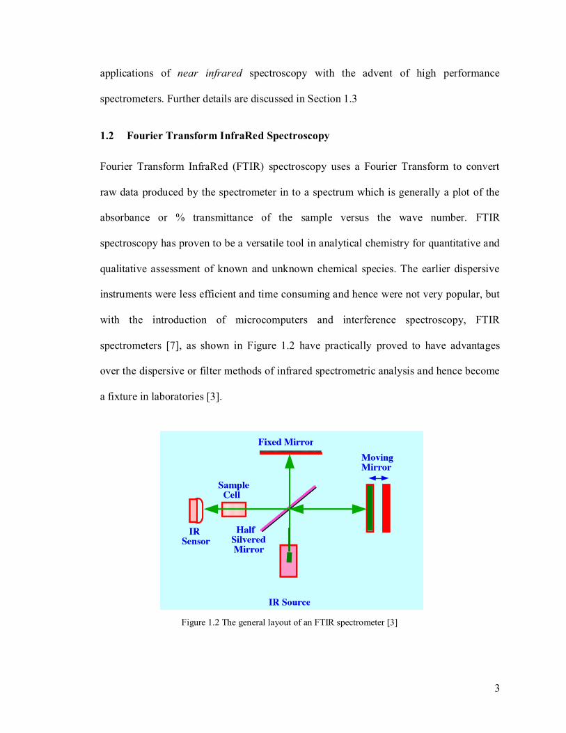


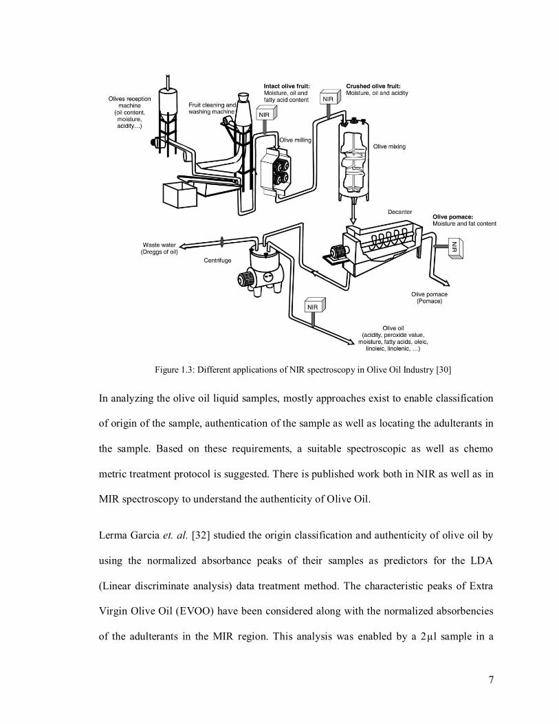

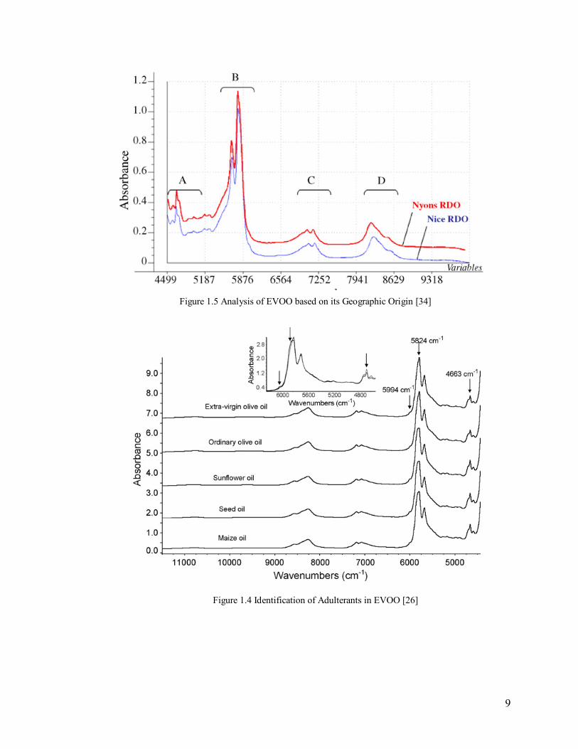

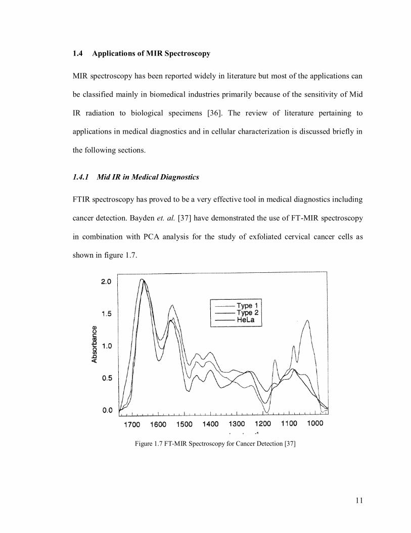


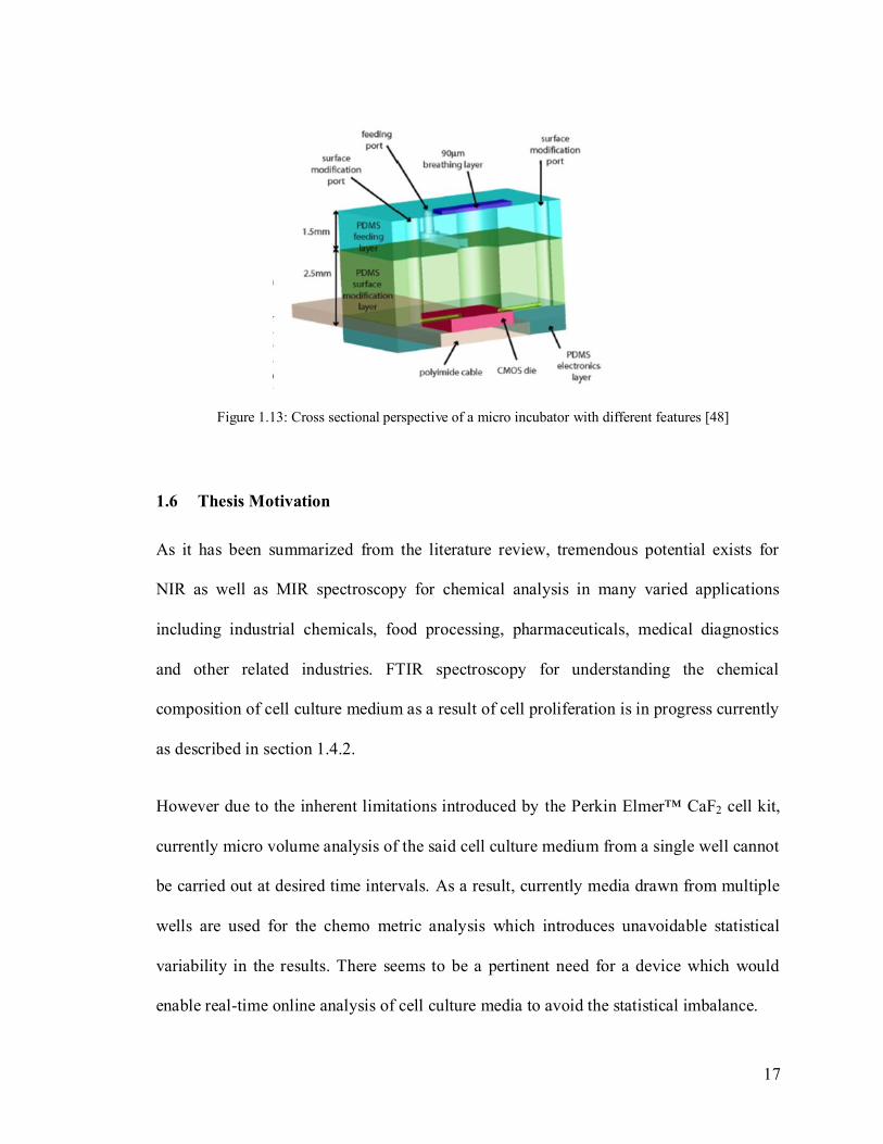


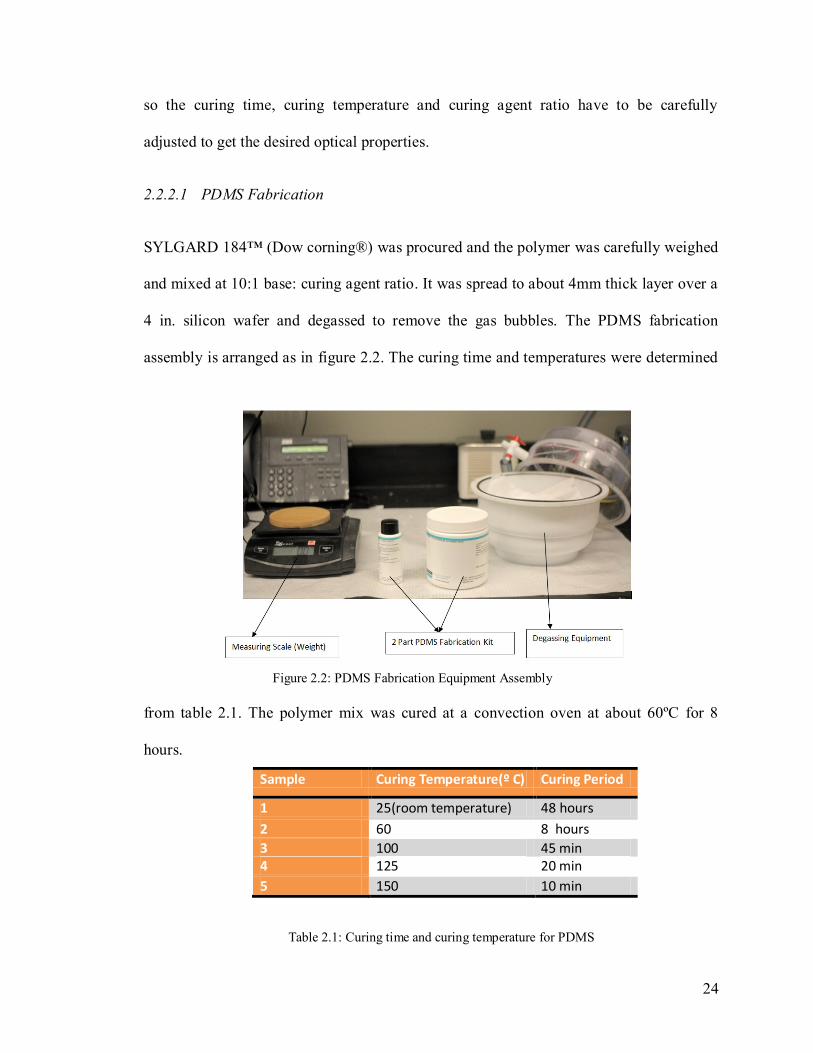

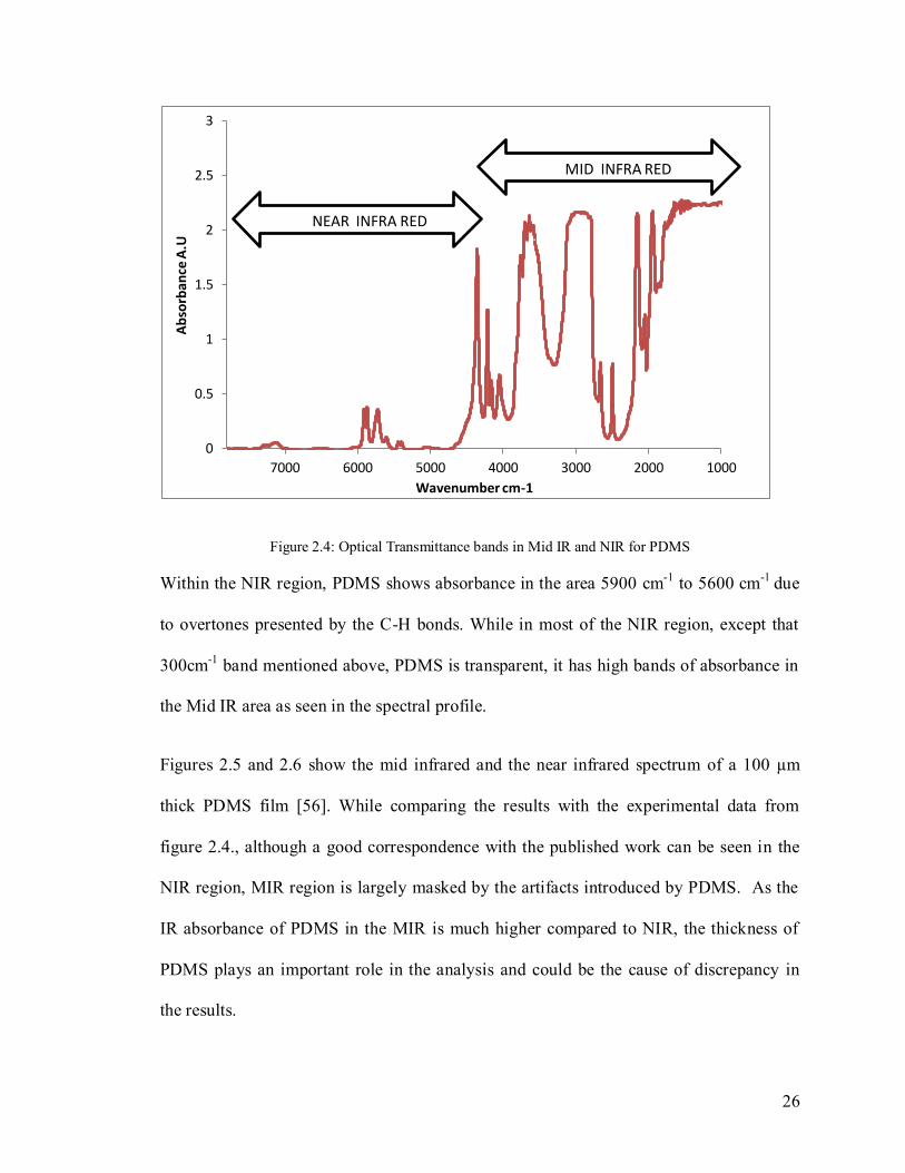
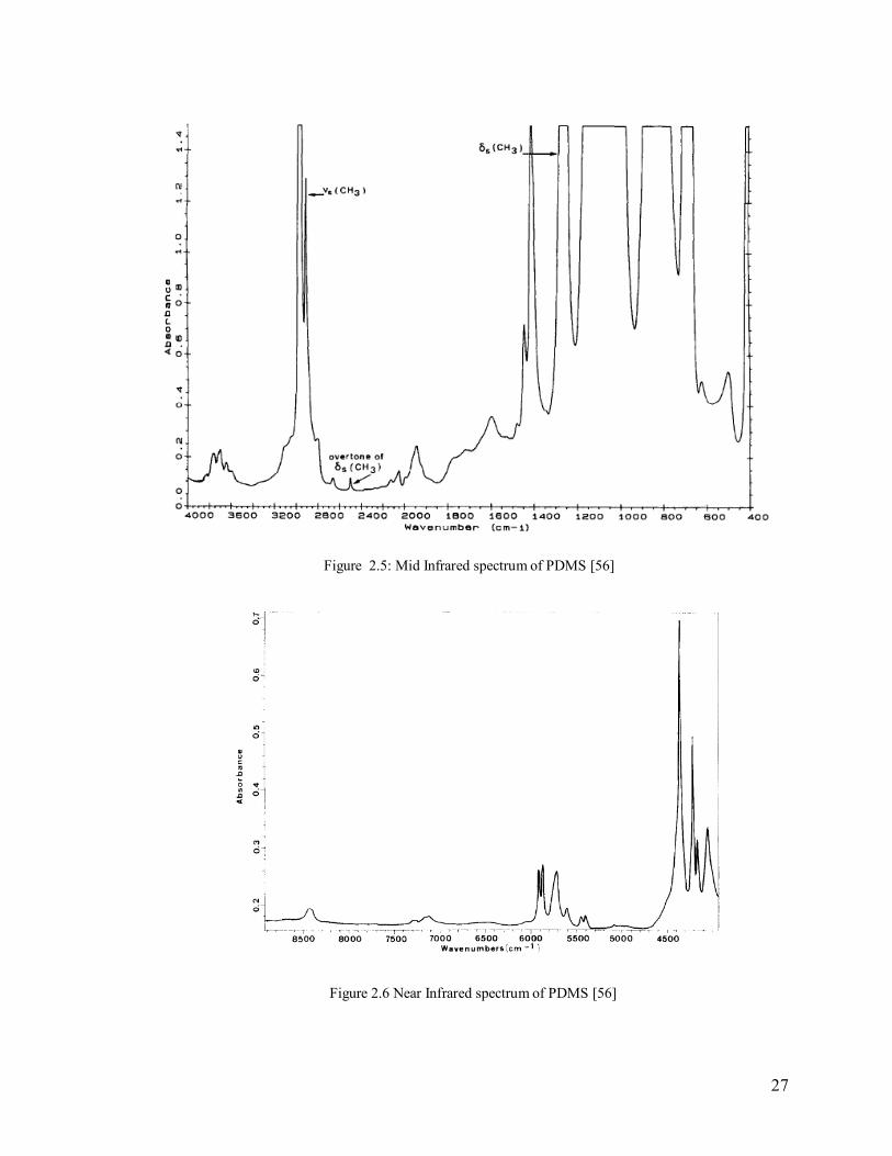


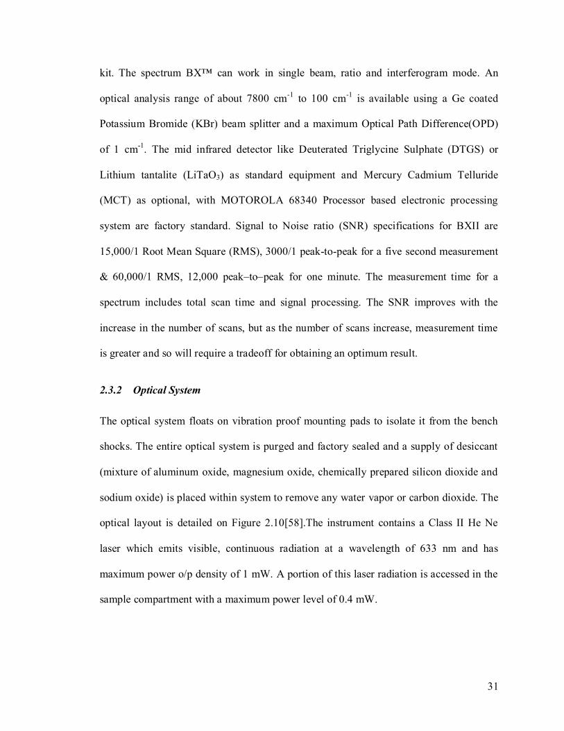


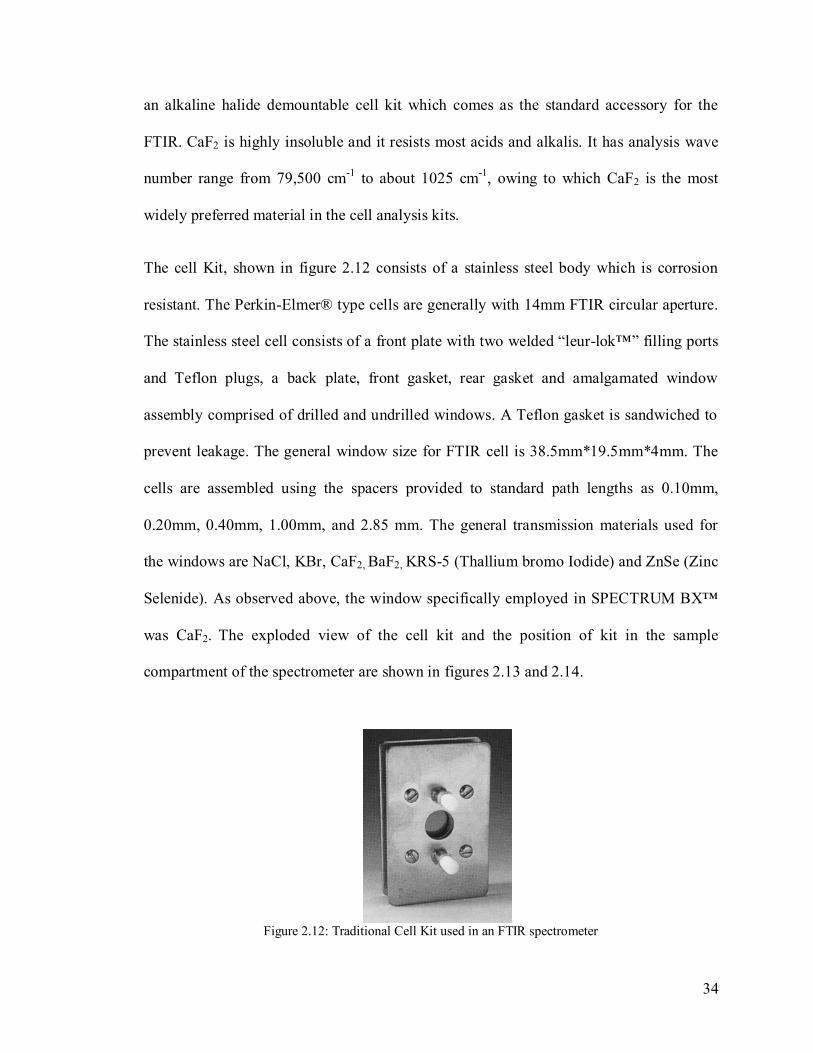


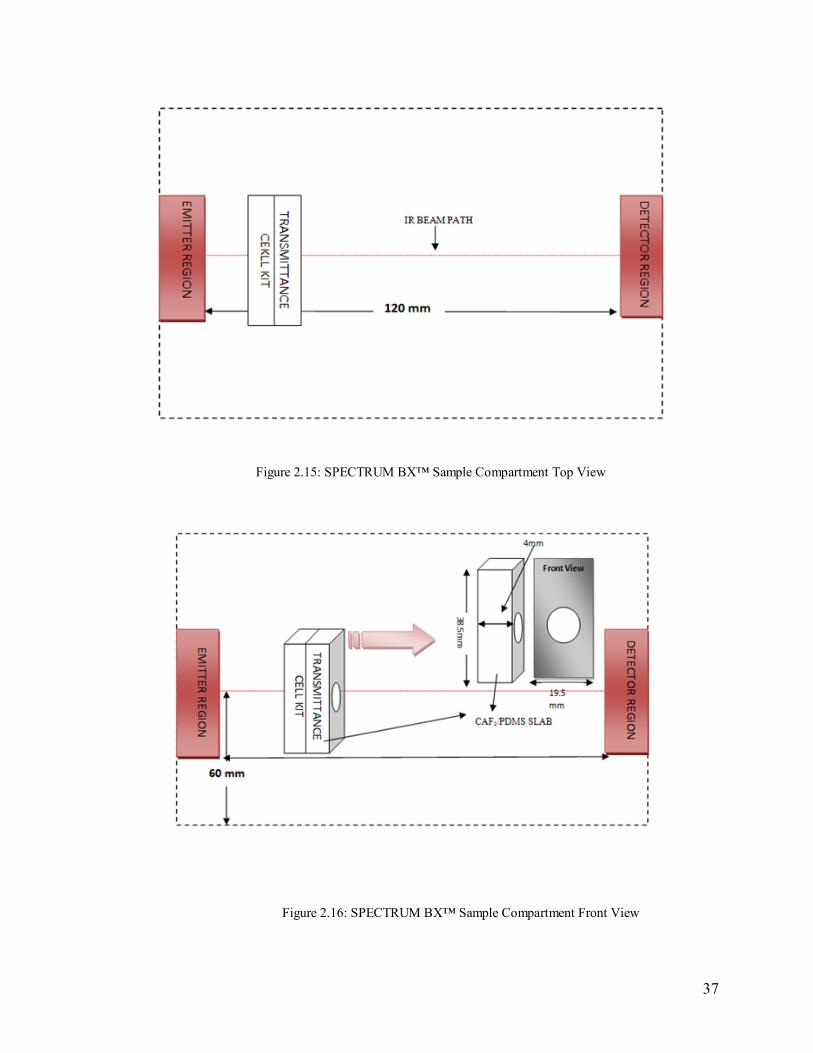
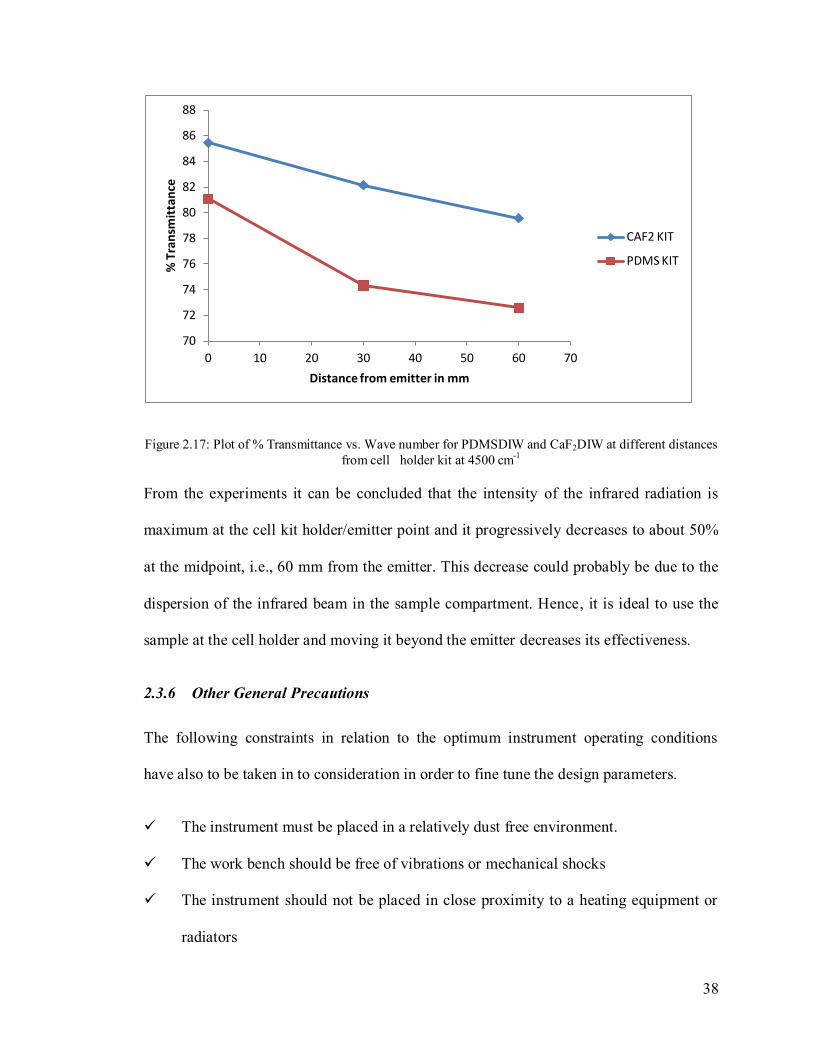

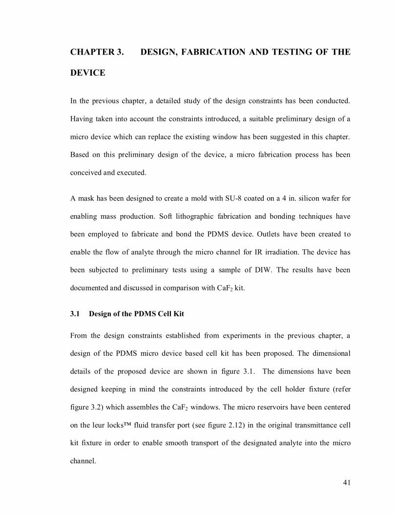
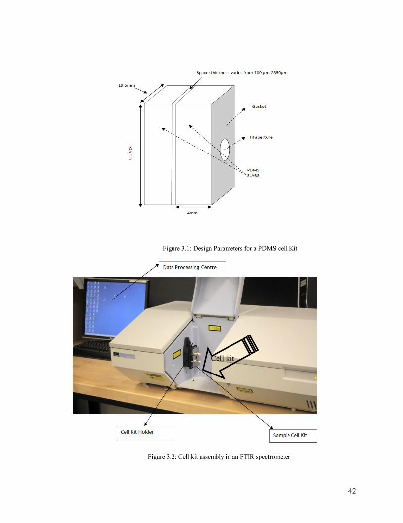
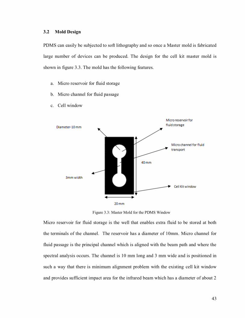
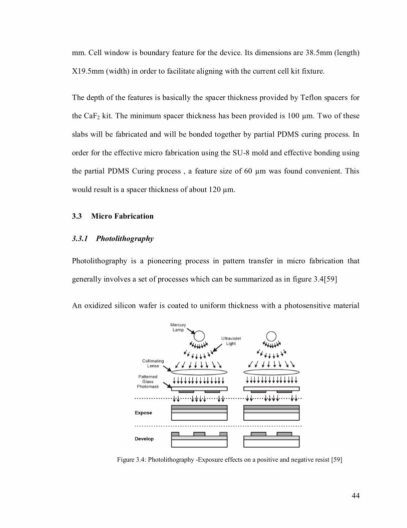
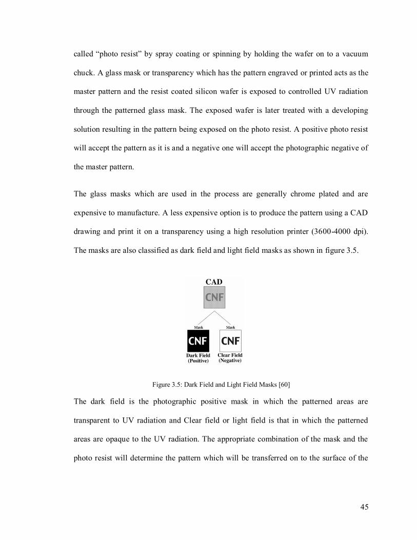

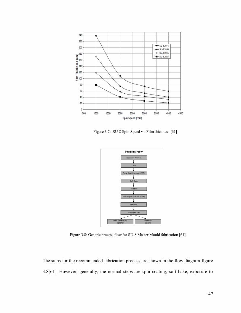


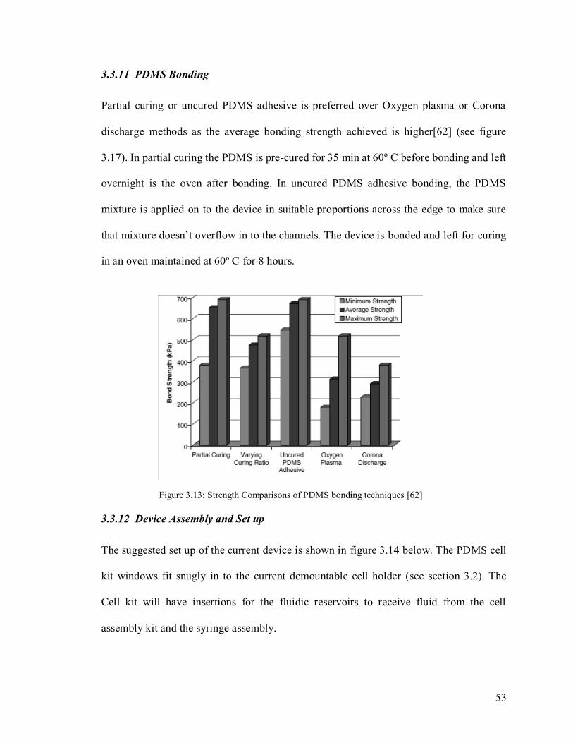


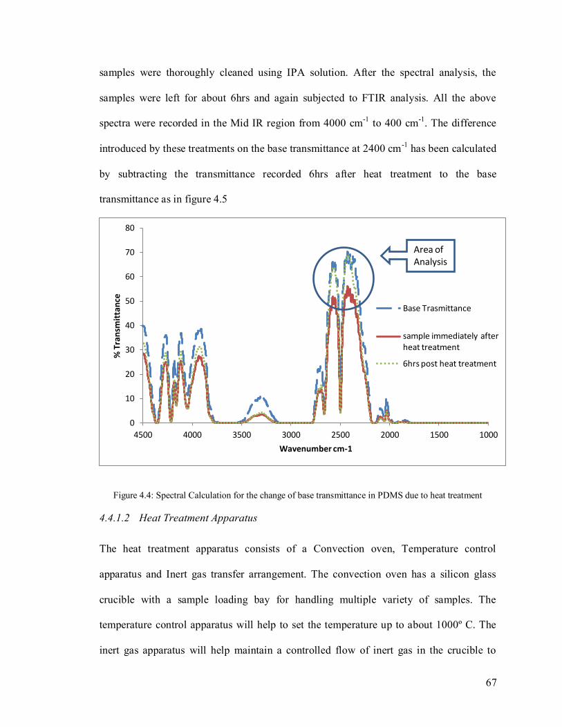
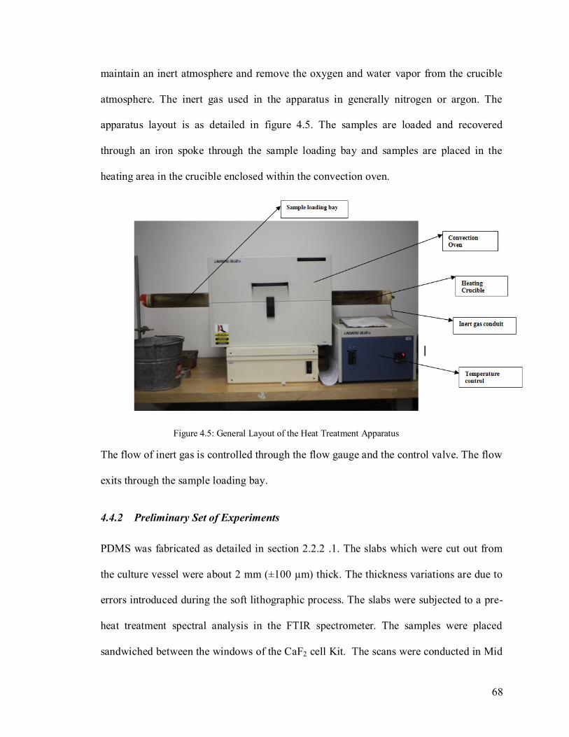


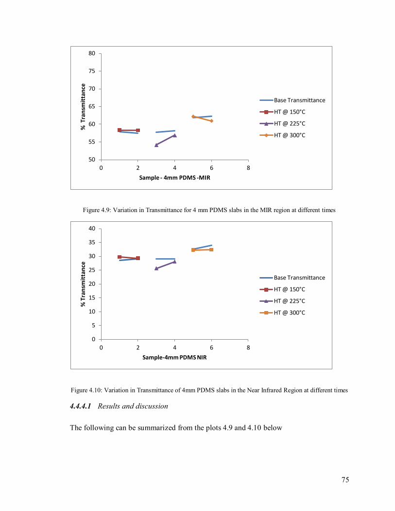
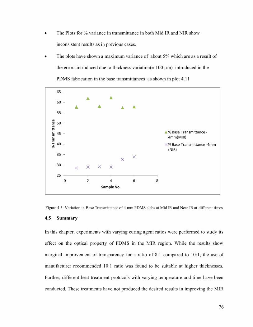
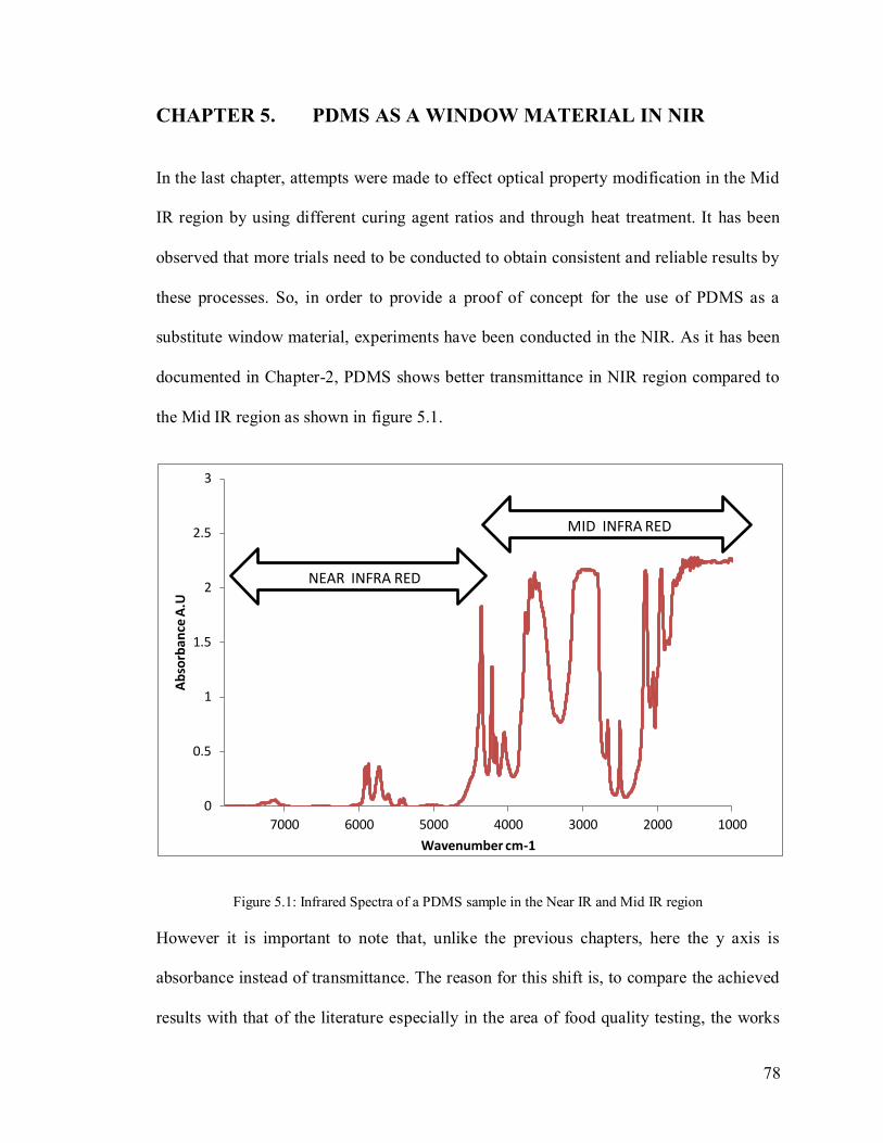


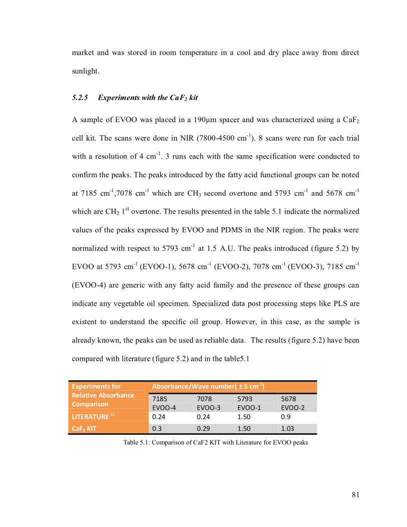
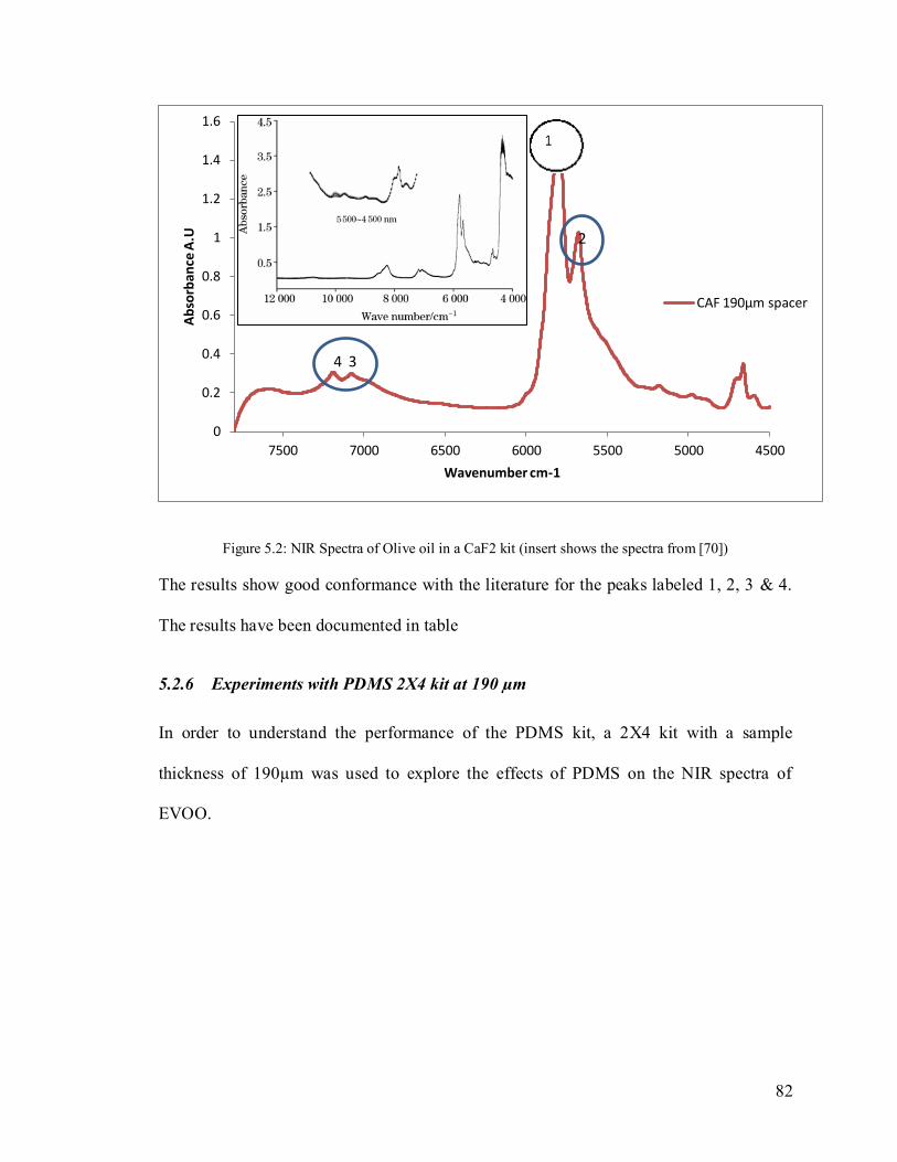


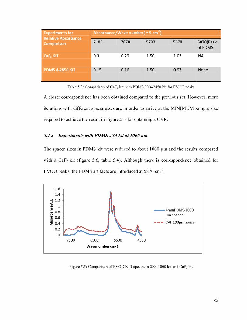
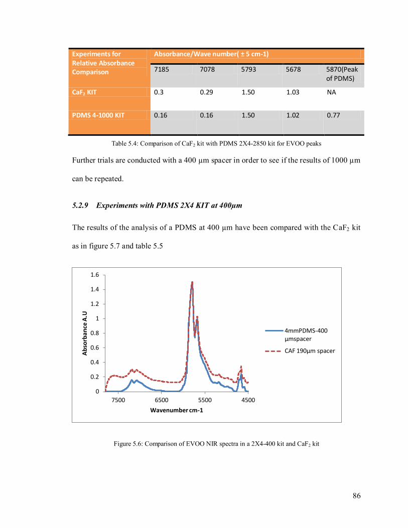
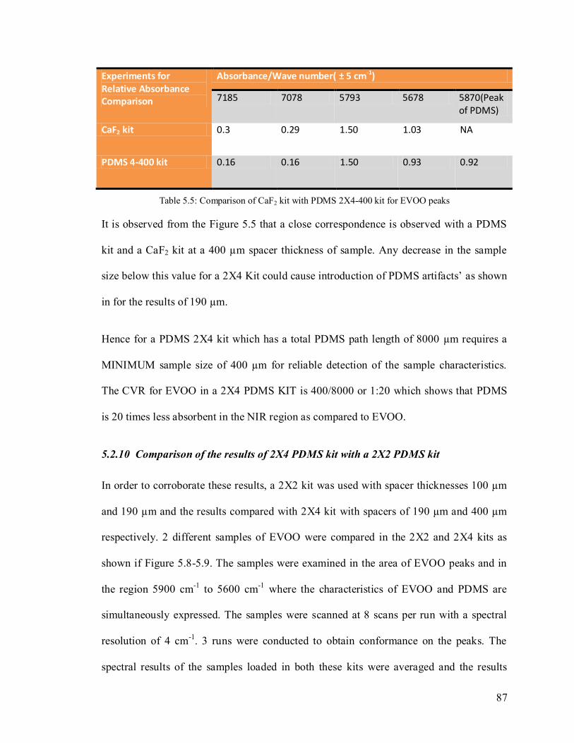
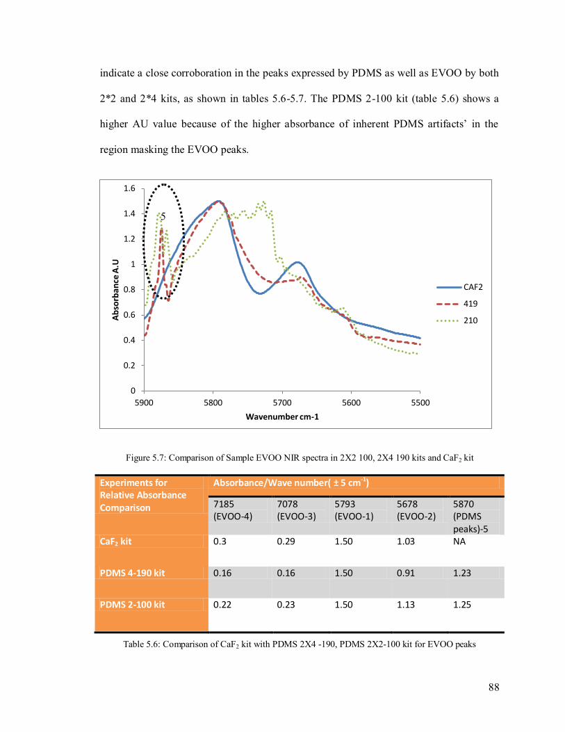


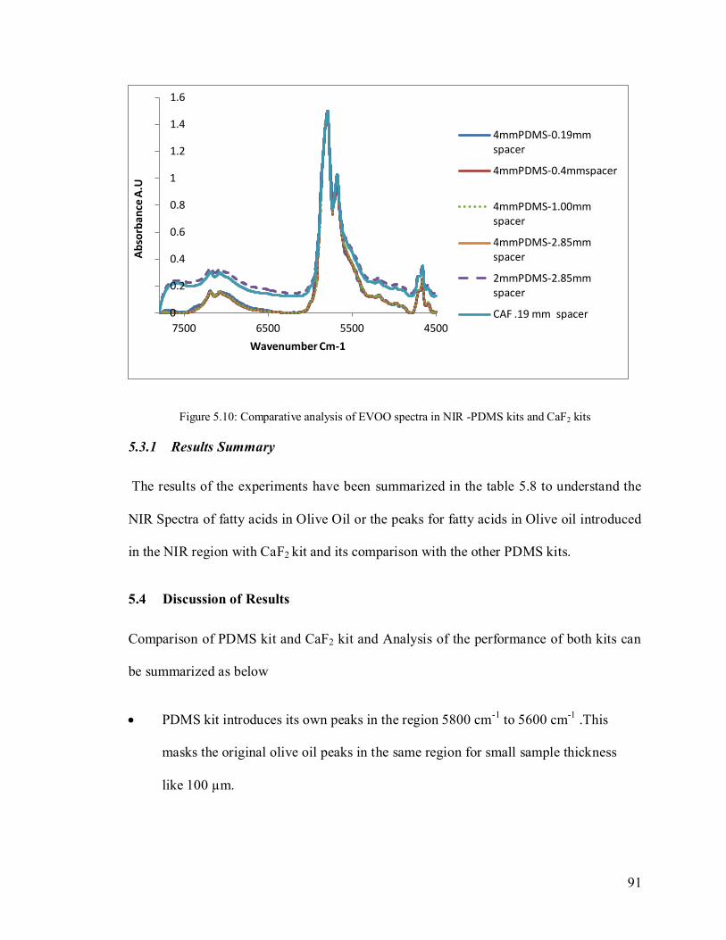


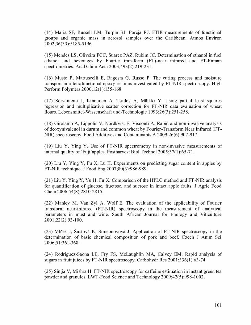

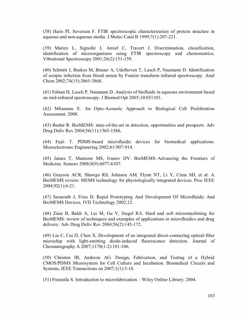


![Poly(dimethylsiloxane) - University Of Marylandpdms).pdf · Poly(dimethylsiloxane) ALEX C. M. KUO ACRONYM, ALTERNATE NAMES, TRADE NAMES PDMS; poly[oxy(dimethylsilylene)]; dimethicone;](https://static.documents.pub/doc/80x56/5a6fad9c7f8b9ab6538b4f50/polydimethylsiloxane-university-of-marylandwwwrubloffgroupumdedupublicationsetcpdh-735pdmspdfpdf.jpg)


