Exar Corporation 48720 Kato Road, Fremont CA, 94538 • (510) 668-7000 • FAX (510) 668-7017 • www.exar.com XRT94L43 SONET/SDH OC-12 TO 12XDS3/E3 MAPPER NOVEMBER 2006 REV. 1.0.2 GENERAL DESCRIPTION The XRT94L43 is an SDH to PDH physical layer processor with integrated SONET OC-12 and 12 DS3/E3 framing controller. The XRT94L43 contains an integral SONET framer which provides framing and error accumulation in accordance with ANSI/ITU- T specifications. For a multiple channel DS3/E3 feature, each channel contains identical elements. The configuration of this device is through internal registers accessible via an 8-bit parallel, memory mapped, microprocessor interface. The SONET/SDH transmit and receive blocks are used to transmit/receive an STS-12/STM-4 signals or compose and decompose 12, STS-1/DS3/E3 signals. The blocks operate at a peak internal clock speed of 77 MHz and support 8-bit internal data paths. The transmit and receive blocks are compliant with both SONET and SDH standards. The XRT94L43 performs all SONET transport and path overhead processing for use in broadband data transport applications. FEATURES • Single Chip solution for 12 DS3/E3 to SONET/SDH Mapping • Generates and terminates SONET section, line and path layers. • Provides SONET frame scrambling and descrambling. • Differential Line Interfaces • 8-bit microprocessor interface • Requires +2.5 and +3.3V power supplies with +5V input tolerance • -40°C to +85°C Operating Temperature Range • Available in a 516 Ball PBGA package APPLICATIONS • Network switches • Concentrators • Frame Relay Switches • SONET Customer Premises Multiplexers • Network Access Equipment • Test/Monitoring Equipment
Transcript
XRT94L43SONET/SDH OC-12 TO 12XDS3/E3 MAPPER
NOVEMBER 2006 REV. 1.0.2
GENERAL DESCRIPTIONThe XRT94L43 is an SDH to PDH physical layer processor with integrated SONET OC-12 and 12 DS3/E3 framing controller. The XRT94L43 contains an integral SONET framer which provides framing and error accumulation in accordance with ANSI/ITU-T specifications. For a multiple channel DS3/E3 feature, each channel contains identical elements. The configuration of this device is through internal registers accessible via an 8-bit parallel, memory mapped, microprocessor interface.
The SONET/SDH transmit and receive blocks are used to transmit/receive an STS-12/STM-4 signals or compose and decompose 12, STS-1/DS3/E3 signals. The blocks operate at a peak internal clock speed of 77 MHz and support 8-bit internal data paths. The transmit and receive blocks are compliant with both SONET and SDH standards.
The XRT94L43 performs all SONET transport and path overhead processing for use in broadband data transport applications.
Exar Corporation 48720 Kato Road, Fremont CA, 94538 • (5
FEATURES
• Single Chip solution for 12 DS3/E3 to SONET/SDH Mapping
• Generates and terminates SONET section, line and path layers.
• Provides SONET frame scrambling and descrambling.
• Differential Line Interfaces
• 8-bit microprocessor interface
• Requires +2.5 and +3.3V power supplies with +5V input tolerance
• -40°C to +85°C Operating Temperature Range
• Available in a 516 Ball PBGA package
APPLICATIONS
• Network switches
• Concentrators
• Frame Relay Switches
• SONET Customer Premises Multiplexers
• Network Access Equipment
• Test/Monitoring Equipment
10) 668-7000 • FAX (510) 668-7017 • www.exar.com
XRT94L43REV. 1.0.2 SONET/SDH OC-12 TO 12XDS3/E3 MAPPER
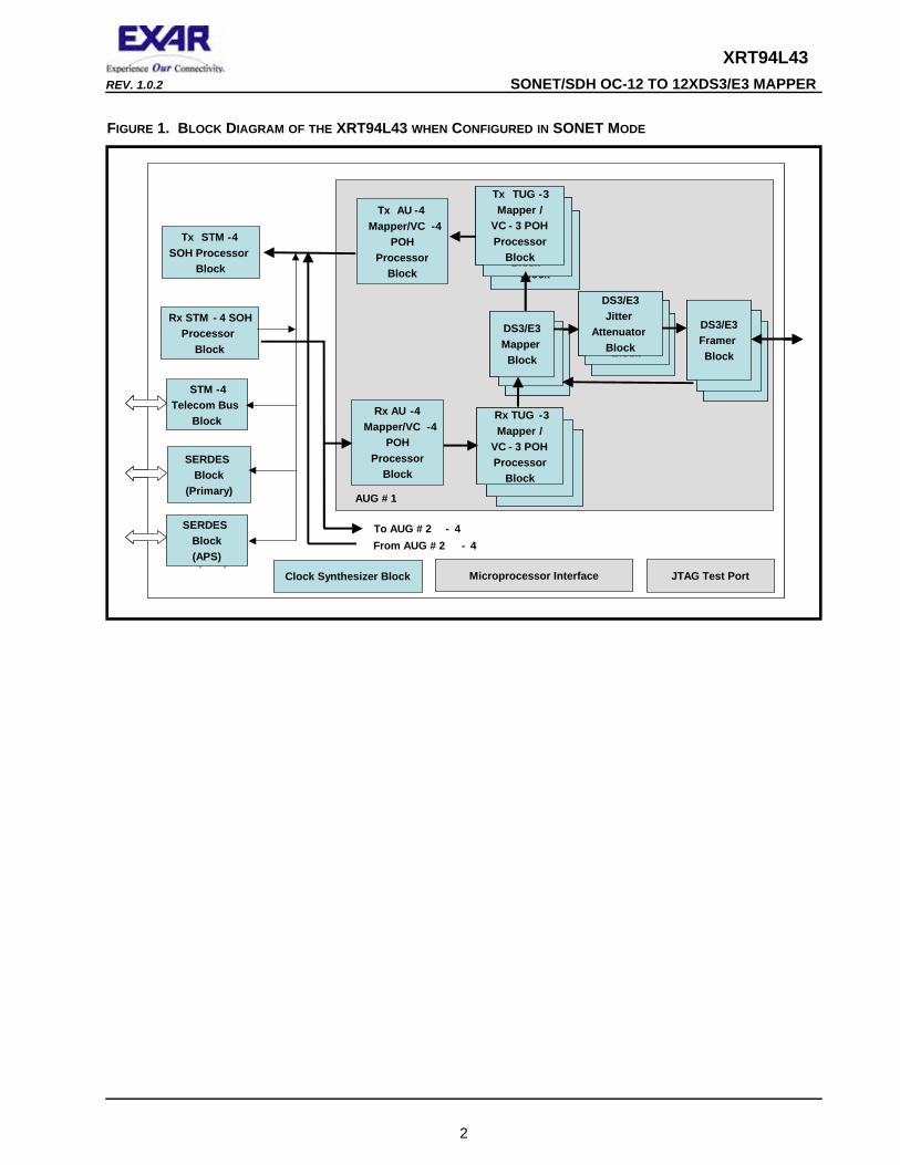
FIGURE 1. BLOCK DIAGRAM OF THE XRT94L43 WHEN CONFIGURED IN SONET MODE
Tx STM -4SOH Processor
Block
Tx STM -4SOH Processor
Block
STM -4Telecom Bus
Block
STM -4Telecom Bus
Block
SERDESBlock
(Primary)
SERDESBlock
(Primary)
SERDESBlock(APS)
SERDESBlock(APS)
Clock Synthesizer BlockClock Synthesizer Block
AUG # 1
To AUG # 2 - 4
Microprocessor InterfaceMicroprocessor Interface JTAG Test PortJTAG Test Port
Rx STM - 4 SOHProcessor
Block
Rx STM - 4 SOHProcessor
Block
From AUG # 2 - 4
DS3/E3Jitter
AttenuatorBlock
DS3/E3Jitter
AttenuatorBlock DS3/E3
FramerBlock
DS3/E3FramerBlock
DS3/E3FramerBlock
DS3/E3FramerBlock
DS3/E3FramerBlock
DS3/E3FramerBlockDS3/E3
MapperBlock
DS3/E3Mapper
Block
DS3/E3Mapper
Block
DS3/E3Mapper
Block
DS3/E3Mapper
Block
DS3/E3Mapper
Block
Rx TUG -3Mapper /
VC - 3 POHProcessor
Block
Rx TUG -3Mapper /
VC - 3 POHProcessor
Block
Tx VC -3POH
ProcessorBlock
Tx VC -3POH
ProcessorBlock
Tx TUG -3Mapper /
VC - 3 POHProcessor
Block
Tx TUG -3Mapper /
VC - 3 POHProcessor
Block
Tx AU -4Mapper/VC -4
POHProcessor
Block
Tx AU -4Mapper/VC -4
POHProcessor
Block
Rx AU -4Mapper/VC -4
POHProcessor
Block
Rx AU -4Mapper/VC -4
POHProcessor
Block
Tx STM -4SOH Processor
Block
Tx STM -4SOH Processor
Block
STM -4Telecom Bus
Block
STM -4Telecom Bus
Block
SERDESBlock
(Primary)
SERDESBlock
(Primary)
SERDESBlock(APS)
SERDESBlock(APS)
Clock Synthesizer BlockClock Synthesizer Block
AUG # 1
To AUG # 2 - 4
Microprocessor InterfaceMicroprocessor Interface JTAG Test PortJTAG Test Port
Rx STM - 4 SOHProcessor
Block
Rx STM - 4 SOHProcessor
Block
From AUG # 2 - 4
DS3/E3Jitter
AttenuatorBlock
DS3/E3Jitter
AttenuatorBlock
DS3/E3Jitter
AttenuatorBlock
DS3/E3Jitter
AttenuatorBlock DS3/E3
FramerBlock
DS3/E3FramerBlock
DS3/E3FramerBlock
DS3/E3FramerBlock
DS3/E3FramerBlock
DS3/E3FramerBlockDS3/E3
FramerBlock
DS3/E3FramerBlock
DS3/E3FramerBlock
DS3/E3FramerBlock
DS3/E3FramerBlock
DS3/E3FramerBlockDS3/E3
MapperBlock
DS3/E3Mapper
Block
DS3/E3Mapper
Block
DS3/E3Mapper
Block
DS3/E3Mapper
Block
DS3/E3Mapper
BlockDS3/E3Mapper
Block
DS3/E3Mapper
Block
DS3/E3Mapper
Block
DS3/E3Mapper
Block
DS3/E3Mapper
Block
DS3/E3Mapper
Block
Rx TUG -3Mapper /
VC - 3 POHProcessor
Block
Rx TUG -3Mapper /
VC - 3 POHProcessor
Block
Rx TUG -3Mapper /
VC - 3 POHProcessor
Rx TUG -3Mapper /
VC - 3 POHProcessor
Block
Tx VC -3POH
ProcessorBlock
Tx VC -3POH
ProcessorBlock
Tx TUG -3Mapper /
VC - 3 POHProcessor
Block
Tx TUG -3Mapper /
VC - 3 POHProcessor
Block
Tx VC -3POH
ProcessorBlock
Tx VC -3POH
ProcessorBlock
Tx TUG -3Mapper /
VC - 3 POHProcessor
Block
Tx TUG -3Mapper /
VC - 3 POHProcessor
Block
Tx AU -4Mapper/VC -4
POHProcessor
Block
Tx AU -4Mapper/VC -4
POHProcessor
Block
Rx AU -4Mapper/VC -4
POHProcessor
Block
Rx AU -4Mapper/VC -4
POHProcessor
Block
2
XRT94L43 SONET/SDH OC-12 TO 12XDS3/E3 MAPPER REV. 1.0.2
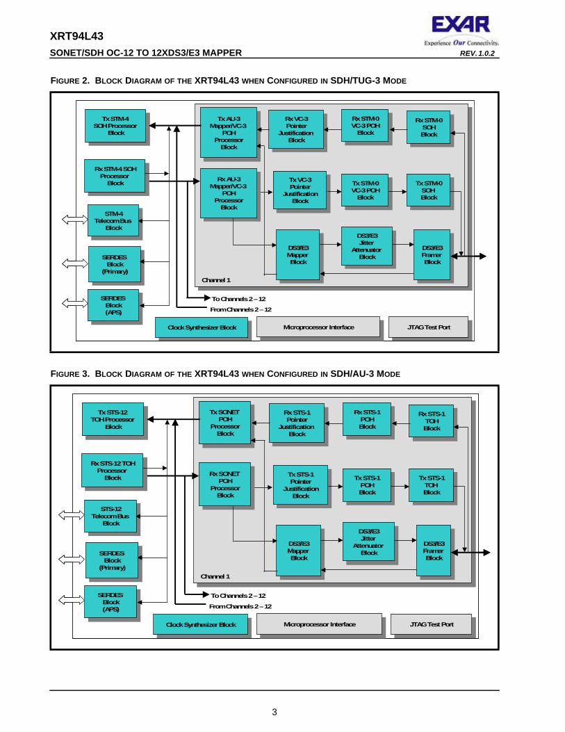
FIGURE 2. BLOCK DIAGRAM OF THE XRT94L43 WHEN CONFIGURED IN SDH/TUG-3 MODE
FIGURE 3. BLOCK DIAGRAM OF THE XRT94L43 WHEN CONFIGURED IN SDH/AU-3 MODE
DS3/E3Framer Block
DS3/E3Framer Block
Rx VC-3Pointer
Justification Block
Rx VC-3Pointer
Justification Block
Rx STM-0VC-3 POH
Block
Rx STM-0VC-3 POH
Block
TxSTM-0VC-3 POH
Block
TxSTM-0VC-3 POH
Block
TxVC-3Pointer
JustificationBlock
TxVC-3Pointer
JustificationBlock
TxSTM-0SOH Block
TxSTM-0SOH Block
Rx STM-0SOHBlock
Rx STM-0SOHBlock
DS3/E3Jitter
Attenuator Block
DS3/E3Jitter
Attenuator Block
DS3/E3Mapper Block
DS3/E3Mapper Block
TxAU-3Mapper/VC-3
POHProcessor
Block
TxAU-3Mapper/VC-3
POHProcessor
Block
TxSTM-4 SOH Processor
Block
TxSTM-4 SOH Processor
Block
STM-4Telecom Bus
Block
STM-4Telecom Bus
Block
SERDES Block
(Primary)
SERDES Block
(Primary)
SERDES Block(APS)
SERDES Block(APS)
Clock Synthesizer BlockClock Synthesizer Block
Channel 1
To Channels 2 –12
Microprocessor InterfaceMicroprocessor Interface JTAG Test PortJTAG Test Port
Rx AU-3Mapper/VC-3
POHProcessor
Block
Rx AU-3Mapper/VC-3
POHProcessor
Block
Rx STM-4 SOHProcessor
Block
Rx STM-4 SOHProcessor
Block
From Channels 2 –12
DS3/E3Framer Block
DS3/E3Framer Block
Rx VC-3Pointer
Justification Block
Rx VC-3Pointer
Justification Block
Rx STM-0VC-3 POH
Block
Rx STM-0VC-3 POH
Block
TxSTM-0VC-3 POH
Block
TxSTM-0VC-3 POH
Block
TxVC-3Pointer
JustificationBlock
TxVC-3Pointer
JustificationBlock
TxSTM-0SOH Block
TxSTM-0SOH Block
Rx STM-0SOHBlock
Rx STM-0SOHBlock
DS3/E3Jitter
Attenuator Block
DS3/E3Jitter
Attenuator Block
DS3/E3Mapper Block
DS3/E3Mapper Block
TxAU-3Mapper/VC-3
POHProcessor
Block
TxAU-3Mapper/VC-3
POHProcessor
Block
TxSTM-4 SOH Processor
Block
TxSTM-4 SOH Processor
Block
STM-4Telecom Bus
Block
STM-4Telecom Bus
Block
SERDES Block
(Primary)
SERDES Block
(Primary)
SERDES Block(APS)
SERDES Block(APS)
Clock Synthesizer BlockClock Synthesizer Block
Channel 1
To Channels 2 –12
Microprocessor InterfaceMicroprocessor Interface JTAG Test PortJTAG Test Port
Rx AU-3Mapper/VC-3
POHProcessor
Block
Rx AU-3Mapper/VC-3
POHProcessor
Block
Rx STM-4 SOHProcessor
Block
Rx STM-4 SOHProcessor
Block
From Channels 2 –12
DS3/E3Framer Block
DS3/E3Framer Block
Rx STS-1Pointer
Justification Block
Rx STS-1Pointer
Justification Block
Rx STS-1POHBlock
Rx STS-1POHBlock
TxSTS-1POHBlock
TxSTS-1POHBlock
TxSTS-1Pointer
JustificationBlock
TxSTS-1Pointer
JustificationBlock
TxSTS-1TOH Block
TxSTS-1TOH Block
Rx STS-1TOHBlock
Rx STS-1TOHBlock
DS3/E3Jitter
Attenuator Block
DS3/E3Jitter
Attenuator Block
DS3/E3Mapper Block
DS3/E3Mapper Block
TxSONET POH
ProcessorBlock
TxSONET POH
ProcessorBlock
TxSTS-12 TOH Processor
Block
TxSTS-12 TOH Processor
Block
STS-12Telecom Bus
Block
STS-12Telecom Bus
Block
SERDES Block
(Primary)
SERDES Block
(Primary)
SERDES Block(APS)
SERDES Block(APS)
Clock Synthesizer BlockClock Synthesizer Block
Channel 1
To Channels 2 –12
Microprocessor InterfaceMicroprocessor Interface JTAG Test PortJTAG Test Port
Rx SONET POH
ProcessorBlock
Rx SONET POH
ProcessorBlock
Rx STS-12 TOHProcessor
Block
Rx STS-12 TOHProcessor
Block
From Channels 2 –12
3
XRT94L43REV. 1.0.2 SONET/SDH OC-12 TO 12XDS3/E3 MAPPER
PRODUCT FEATURESSONET TRANSMITTER
• Generates and Transmits Standard STS-12/STM-4 data
• Generates and Transmits either an STM-4/TUG-3 or STM-4/AU-3 signals for SDH applications
• Conforms to ITU-T 1.432, ANSI T1.105 and Bellcore GR-253 Standards
• Performs SONET frame insertion and accepts external frame synchronization
• Performs Optional Transmit Data Scrambling
• Permits the user to externally insert their own values for the POH and TOH into the outbound STS-12/STM-4 traffic
• Generates transmit payload pointer (H1,H2) (fixed at 522) with NDF insertion
• Inserts A1/A2 with optional error mask
• Computes and inserts BIP-8 (B1,B2) with optional error mask
• Generates and transmits REI-L and RDI-L either upon Software Command or automatically based upon errors and defects that are detected/declared by the SONET Receiver.
• Permits the user to transmit the LOS pattern via Software Command.
• Generates and transmits RDI-P and REI-P either upon Software Command or automatically based upon errors and defects that are detected/declared by the SONET Receiver.
• Inserts the fixed-stuff columns, calculates and inserts the B3 byte value into each outbound STS-1 SPE/VC-3 or STS-3c SPE/VC-4
SONET RECEIVER
• Receives and processes standard STS-12/STM-4 signals
• Receives and processes either an STM-4/TUG-3 or STM-4/AU-3 signal for SDH Applications
• Permits the user to fully program the B2 Byte Error-rate thresholds for declaration and clearance of the SD and SF defect conditions
• Provides section trace buffer with mismatch detection and invalid message detection
• Performs SONET Frame Synchronization
• Supports NDF, positive stuff and negative stuff for pointer processor
• Performs receive data de-scrambling
• Performs POH and TOH interpretation/extraction
• Interprets payload pointer (H1,H2)
• Extracts data communication channels from D1-D3 and D4-D12
• Declares and Clears the SEF (Severely Erred Frame), LOF (Loss of Frame) and LOS (Loss of Signal) defect conditions
• Declares and clears the Line AIS (AIS-L) and the Line Remote Defect Indicator (RDI-L) defect conditions
• Declares and Clears the Path - AIS (AIS-P), Loss of Pointer (LOP-P) and Path - Unequipped (UNEQ-P) defect conditions.
• Supports either the Single-Bit or Extended form of RDI-P
• Monitors the Path Signal Label and declares/clears the PLM-P defect condition
4
XRT94L43 SONET/SDH OC-12 TO 12XDS3/E3 MAPPER REV. 1.0.2
• Contains 12 on-chip 64 byte Expected Receive Path Trace Message Buffer, in which the user will load in an expected Path Trace Message
• Contains 12 on-chip 64 byte Actual" Receive Path Trace Message Buffers, that will contain the actual Received Path Trace Message
• The SONET Receiver will use the contents within both the Expected and Actual Receive Path Trace Message Buffers to either declare or clear the TIM-P defect condition
• Computes and verifies the B3 bytes within each incoming STS-1 SPE/VC-3 or STS-3c SPE/VC-4 and increments on-chip Performance Monitoring registers each time it detects B3 byte errors.
• Detects and Flags Line - Remote Error Indicator (REI-L) and Path - Remote Error Indicator (REI-P) events, and increments on-chip Performance Monitoring registers each time it detects REI-L or REI-P events
• Computes and verifies both the B1 and B2 bytes within the incoming STS-12/STM-4 data-stream and increments on-chip Performance Monitoring registers each time it detects B1 or B2 byte errors
MAPPER
• Maps DS3 data into/De-maps DS3 data from an STS-1 SPE per the requirements in Telcordia GR-253-CORE
• Maps DS3/E3 data into/De-Maps DS3/E3 data from a VC-3 per ITU-T G.707
• Implements AU-3 to VC-3 multiplexing and de-multiplexing
DS3 RECEIVE FRAMER
• Offers off-line framing algorithm
• Complies with the standards as: Bellcore TR-NWT-000499 and TR-NWT-000009
• Supports overhead extraction
• Detects and flags LCV (Line Code Violations) and EXZ (Excessive Zero Events).
• Reports and counts FEBE
• HDLC controller complies with ITU-T Q.921 LAPD protocol
• Provides Line and Local Loop-backs
• Supports either the M13 or the C-bit Parity Framing formats
• Supports B3ZS line decoding which can be user enabled.Replaces valid B0V or 00V with 3 zeros
• Synchronizes to incoming frame based upon 10 valid F bits followed by 3 consecutive valid M frames, Offers optional AIC-bit or parity verification before declaration of sync
• Detects Out of Frame (OOF) upon 3 or 6 F bits out of 15 F bits in error or 1 or more M bits in 3 of 4 consecutive frames in error
• Detects Loss of Signal (LOS) upon encountering 180 consecutive 0’s and clears on at least 60 of successive received 1’s.Offers optional disable
• Detects idle state by checking C-bit in subframe 3 are all zero, X-bits are one and repeating 11001100 payloads. Declaration occurs when all the above conditions persist for 63 M-frames. Clears the condition when 63 valid M-frames are received
• Detects AIS with different algorithm
• Computes and verifies P and CP-Bits
• Validate FERF bits, sets to one when both X-bits are zero and clears when they are One
• Detects and validates FEAC codes upon 8 out of 10 last identical received codes.Invalidates on 3 in 10 mismatch
5
XRT94L43REV. 1.0.2 SONET/SDH OC-12 TO 12XDS3/E3 MAPPER
• Provides 15-bit PRBS lock
DS3 TRANSMIT FRAMER
• Offers following frame generation mechanism: Asynchronous operation, using receive side clock, external framing
• Supports either C-bit operation or M13 operation: optional all C bits set to "1" or C-bit parity ID bit (C11) toggled in each frame for M13 operation
• Provides start of frame control with external pin
• Inserts frame overhead bits via External serial port or Internal generation
• Generates and checks parity
• Automatically transmits the DS3 FERF/REI indicator whenever the DS3 Receiver declares either the DS3 LOS, DS3 AIS or DS3 OOF defect conditions.
• Permits the user to control the DS3 FEBE/REI bit-fields via Software Control, or to automatically transmit the FEBE/REI indicator whenever the DS3 Receiver detects CP-Bit or Framing (F or M) bit errors
• Provides FEAC channel processing including generation of valid FEAC patterns and transmissions of all 1’s upon programming of idle code
• Inserts path maintenance data link through HDLC transmitter which contains the following features:
AM for storage of entire LAPD messageSelection of message length to 82 or 76 bytesOptional frame header generationGeneration of flag sequencesComputation and insertion of CRCZero stuffingRegister bits for communication with microprocessorInterrupt generation upon transmission of message
• LOS Insertion enabled by register bit
• AIS Insertion enabled by register bit or pin
• Idle signal insertion enabled by register bit
• Supports B3ZS encoding
• Generates AIS, Idle and Yellow force alarms
• Inserts errors optionally in the P, F, FEBE and M bits
• Provides 15-bit PRBS generator
E3 RECEIVE FRAMER
• Offers off-line framing algorithm
• Complies with standards as: ITU-T G.751 and G.832
• Provides line code violation detection and excess zero count
• LAPD controller complies with ITU Q.921 LAPD protocol
• Provides local loop-back
• Supports G.751 and G.832 framing formats
• Supports HDB3 line decoding which can be user enabled. Replaces valid B00V or 000V with 4 zero’s
6
XRT94L43 SONET/SDH OC-12 TO 12XDS3/E3 MAPPER REV. 1.0.2
• Synchronizes to incoming frame based upon occurrence of two sets of FA1, FA2 with expected separation -G.832 or detection of three consecutive frame alignment signals (FAS) - G.751
• Detects Out of Frame (OOF) upon 4 consecutive invalid frames
• Detects Loss of Signal (LOS) upon encountering 32 consecutive 0’s and clears on occurrence of 32 bits without a string of 4 0s
• Detects AIS if 7 or less 0s detected in each of 2 consecutive frames and clears if more than seven 0’s detected in each of 2 consecutive frames
• Calculation and comparison of BIP-8 (G.832) or BIP-4 (G.751). BIP-4 calculation can be disabled
• Supports overhead extraction
• Microprocessor access to TR trail trace message - 16 TTB registers (G.832) or service (Alarm and Nation) bits (G.751)
• Detects MA FERF if 3 or 5 consecutive MA MSBs are 1and clears if 3 or 5 consecutive MA MSBs are 0 (only E3 G.832)
• Indicates last validated FERF value and interrupt upon a change in validated FERF value
• Extracts payload type (MA) bits and stores in a register (Only E3 G.832)
• Extracts Timing Marker bit and checks for consistency over 3 or 5 consecutive frames (only E3 G.832)
• Extracts Synchronous Status Message bits and stores it in register bits when enabled (only G.832)
• Overhead output on synchronous serial interface
E3 TRANSMIT FRAMER
• Offers following frame generation mechanism: Asynchronous operation, using receive side clock, external framing
• Supports either G.751 or G.832 framing format
• Generates and checks parity BIP-8 (G.832), BIP-4 (G.751) BIP-4 computation can be disabled
• Inserts data link message through E3 data line channel which contains the following features:
Insertion into NR or GC byte (programmable through register bit) (E3 G.832 only)Insertion into Nation bit in case of E3 G.751 when LAPD is enabledRAM storage of entire LAPD messageSelection of message length to 82 or 76 bytesGeneration of flag sequencesComputation and insertion of CRC-16Zero stuffingRegister bits for communication with microprocessorsInterrupt generation upon complete transmission of message
• LOS insertion enabled by register bit to force all 0s in the transmit stream
• AIS insertion enabled by register bit and/or pin to force all 1’s in the transmit stream
• Supports HDB3 encoding enabled by register bit
• Inserts frame overhead bits via External serial/nibble port (except for FA1,FA2 and EM bytes in case of E3 G.832 and FAS and BIP-4 in case of G.751) or through external overhead interface or from configuration register or internal generation
• Inserts FA1, FA2, EM, TR, MA and GC bytes into G.832 stream or FAS service bits and BIP4 (if enabled) into G.751 stream
7
XRT94L43REV. 1.0.2 SONET/SDH OC-12 TO 12XDS3/E3 MAPPER
• Inserts MA,NR,GC and TR (TTB) from microprocessor accessible registers (service bit for G.751)
• Inserts FEBE in MA upon receipt of EM byte errors.Programmable through register bit (G.832)
• Asserts FERF upon any combination of LOS,OOF or AIS received from receiver (G.832)
• Inserts synchronous status message from microprocessor accessible registers, when enabled (G.832)
• Error masks for framing bytes, and computed parity (BIP-8 in case of G.832 and BIP-4 in case of G.751)
• Optionally accepts overhead bits (except FA bytes for G.832 and FAS bits for G.751) from input interface
E3/DS3/STS-1 DE-JITTERING/DE-SYNC CIRCUIT
• Meets the E3/DS3/STS-1 jitter requirements
• Compliant with jitter transfer template outlined in ITU G.751,G.752,G.755 and GR-499-CORE
• Meets output jitter requirement as specified by ETSI TBR24
• Meets the jitter and wander specifications described in T1.105.03b,GR-253 and GR-499 standards
• Performs the De-synchronizer function and pointer adjustments for STS-1 to DS3 mapping
PERFORMANCE MONITORING
• Supports line and path performance monitoring
• Provides 32-bit saturating counter of OOF errors
• Provides 32-bit saturating counter LOF errors
• Provides 32-bit saturating counter of LOS errors
• Provides 32-bit saturating counter of SD errors
• Provides 32-bit saturating counter of SF errors
• Provides 32-bit saturating counter B3 errors
• Provides 32-bit saturating counter of the line RDI, path AIS,REI-L errors, REI-P errors and BIP-8(B1,B2),B3 errors and loss of pointer
• Provides 16-bit saturating counter of DS3 framing bit errors, DS3 frame parity errors, line code violations, frame parity (BIP) errors, DS3 frame CP bit errors and DS3 Far-End Block errors
• One second statistics
1. Bipolar violations2. Frames with parity errors3. Frames with CP bit errors4. Errored second indication5. Severely errored second indication
INTERRUPT, STATUS AND TEST
• Provides individually maskable interrupts
• Provides one second interrupt generations
• Generates interrupts from the following causes:
• DS3 OOF status change, LOS status change, DS3 AIS status, LAPD message received, DS3 parity error,DS3 FEAC validation, DS3 FEAC removal, DS3 IDLE status change, FEBE (E3) change, DS3 FERF change, DS3 format change (AIC), LAPD end of message transmission and DS3 FEAC end of message transmission, DS3 Framing alignment change, SONET OOF status change and COFA
• Provides local and remote line loopback
8
XRT94L43 SONET/SDH OC-12 TO 12XDS3/E3 MAPPER REV. 1.0.2
• Provides SONET remote loopback
9
XRT94L43REV. 1.0.2 SONET/SDH OC-12 TO 12XDS3/E3 MAPPER
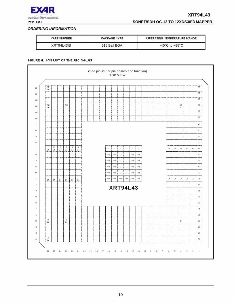
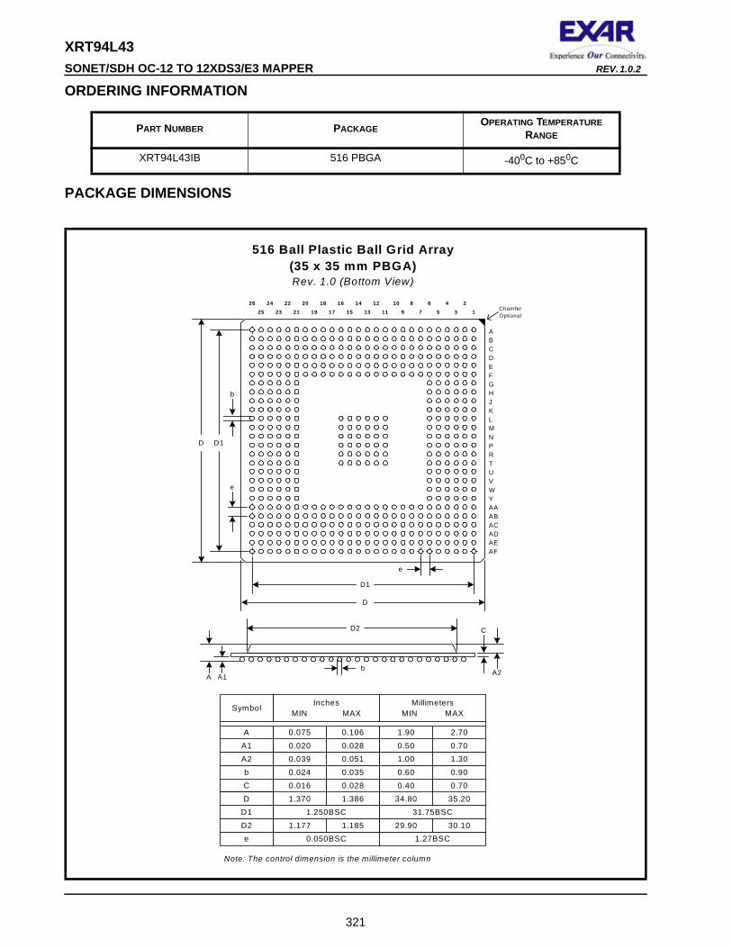
ORDERING INFORMATION
PART NUMBER PACKAGE TYPE OPERATING TEMPERATURE RANGE
XRT94L43IB 516 Ball BGA -40°C to +85°C
FIGURE 4. PIN OUT OF THE XRT94L43
(See pin list for pin names and function)TOP VIEW
A
B
C
D
E
F
G
H
J
K
L
M
N
P
R
T
U
V
W
Y
AA
AB
AC
AD
AE
AF
2122 192023242526 123456781718 13141516 9101112
A26
D23
D26
AC1
AC4
AC23
AC26
AF1
AF26
AE1
AD1
A1
D1D4
C1
B1
L4
T4
E1
F1
G1
H1
J1
K1
L1
M1
AA1
AB1
U1
V1
W 1
Y1
N1
P1
R1
T1
L2
T2
L3
T3
L26
Y26
L23
T23
L24
T24
L25
T225
XRT94L43
V3
G
V1
G
G
G
G
G
G
G
G
G
G
GG
V2
G
V3 V3 V3 V3 V3
V1
V1
V1
V1
V1
V1
V1V2 V2
V2 V2
V2 V2
V2
L22
T22
L21
T21
L6
T6
L5
T5
10
XRT94L43 SONET/SDH OC-12 TO 12XDS3/E3 MAPPER REV. 1.0.2
TABLE OF CONTENTS
GENERAL DESCRIPTION ................................................................................................ 1FEATURES ................................................................................................................................................. 1APPLICATIONS .......................................................................................................................................... 1
FIGURE 1. BLOCK DIAGRAM OF THE XRT94L43 WHEN CONFIGURED IN SONET MODE ..................................................................... 2FIGURE 2. BLOCK DIAGRAM OF THE XRT94L43 WHEN CONFIGURED IN SDH/TUG-3 MODE .............................................................. 3FIGURE 3. BLOCK DIAGRAM OF THE XRT94L43 WHEN CONFIGURED IN SDH/AU-3 MODE................................................................. 3
FIGURE 4. PIN OUT OF THE XRT94L43.......................................................................................................................................... 10TABLE OF CONTENTS ............................................................................................................ IPIN DESCRIPTIONS - DIRECT ADDRESSING ............................................................... 8
MICROPROCESSOR INTERFACE ...................................................................................................................... 8SONET/SDH SERIAL LINE INTERFACE PINS ................................................................................................ 13STS-12/STM-4 TELECOM BUS INTERFACE - TRANSMIT DIRECTION .............................................................. 19STS-12/STM-4 TELECOM BUS INTERFACE - RECEIVE DIRECTION ................................................................ 22SONET/SDH OVERHEAD INTERFACE - TRANSMIT DIRECTION ...................................................................... 24STS-3/STM-1 TELECOM BUS INTERFACE - TRANSMIT DIRECTION ................................................................ 33RXSTS-1 TOH/POH INTERFACE................................................................................................................. 82STS-3/STM-1 TELECOM BUS INTERFACE - RECEIVE DIRECTION .................................................................. 85RECEIVE TRANSPORT OVERHEAD INTERFACE............................................................................................. 128GENERAL PURPOSE INPUT/OUTPUT ........................................................................................................... 135CLOCK INPUTS .......................................................................................................................................... 139BOUNDARY SCAN...................................................................................................................................... 139MISCELLANEOUS PINS............................................................................................................................... 139POWER SUPPLY PINS................................................................................................................................ 140VDD = 3.3V ............................................................................................................................................ 140VDD (2.5V).............................................................................................................................................. 140GROUND................................................................................................................................................... 142NO CONNECTS.......................................................................................................................................... 142
PIN DESCRIPTIONS - INDIRECT ADDRESSING ....................................................... 144MICROPROCESSOR INTERFACE .................................................................................................................. 144SONET/SDH SERIAL LINE INTERFACE PINS .............................................................................................. 146STS-12/STM-4 TELECOM BUS INTERFACE - TRANSMIT DIRECTION ............................................................ 153STS-12/STM-4 TELECOM BUS INTERFACE - RECEIVE DIRECTION .............................................................. 156SONET/SDH OVERHEAD INTERFACE - TRANSMIT DIRECTION .................................................................... 158STS-3/STM-1 TELECOM BUS INTERFACE - TRANSMIT DIRECTION .............................................................. 167RXSTS-1 TOH/POH INTERFACE............................................................................................................... 219STS-3/STM-1 TELECOM BUS INTERFACE - RECEIVE DIRECTION ................................................................ 222RECEIVE TRANSPORT OVERHEAD INTERFACE............................................................................................. 272GENERAL PURPOSE INPUT/OUTPUT ........................................................................................................... 279CLOCK INPUTS .......................................................................................................................................... 287BOUNDARY SCAN...................................................................................................................................... 287MISCELLANEOUS PINS............................................................................................................................... 287
I
XRT94L43REV. 1.0.2 SONET/SDH OC-12 TO 12XDS3/E3 MAPPER
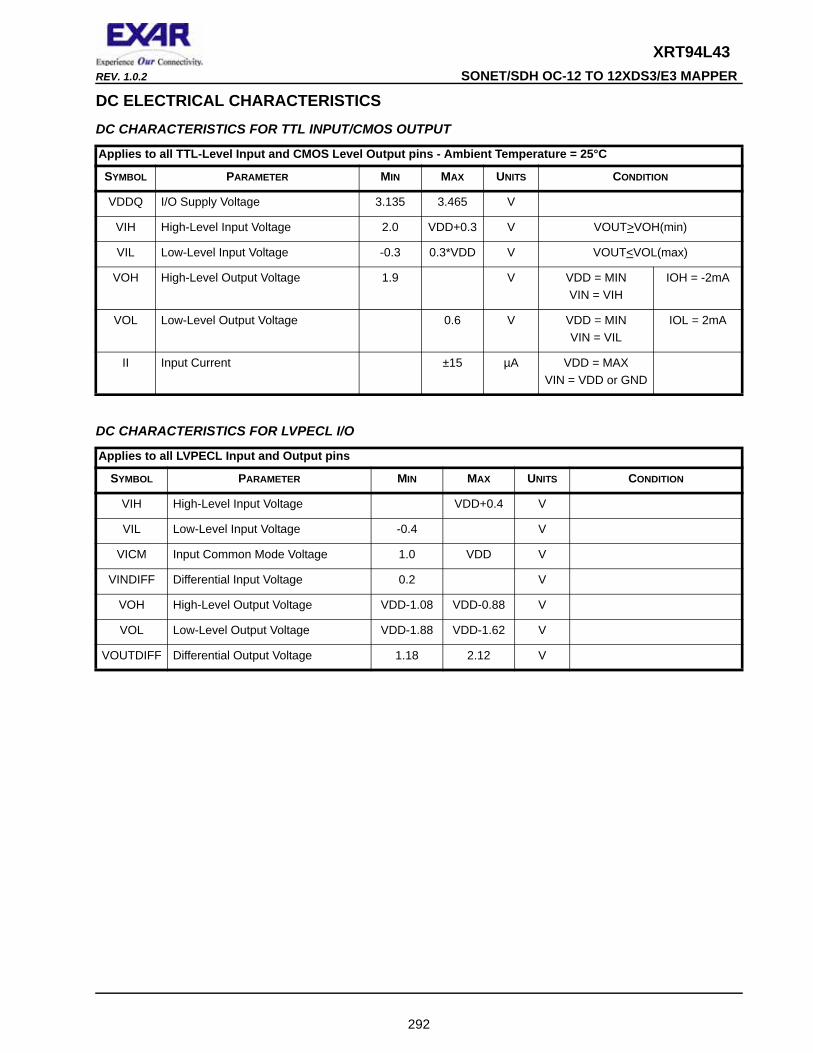
DC ELECTRICAL CHARACTERISTICS ...................................................................... 292DC CHARACTERISTICS FOR TTL INPUT/CMOS OUTPUT ............................................................................. 292DC CHARACTERISTICS FOR LVPECL I/O .................................................................................................. 292
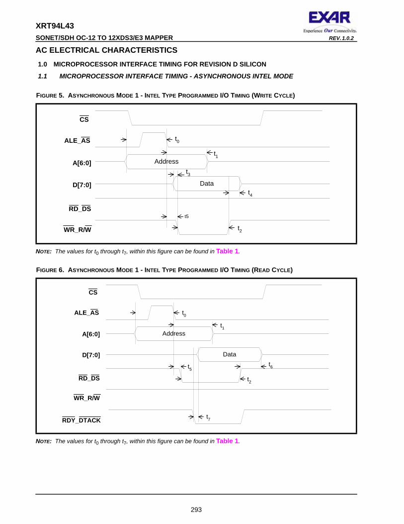
AC ELECTRICAL CHARACTERISTICS....................................................................... 2931.0 MICROPROCESSOR INTERFACE TIMING FOR REVISION D SILICON ......................................... 293
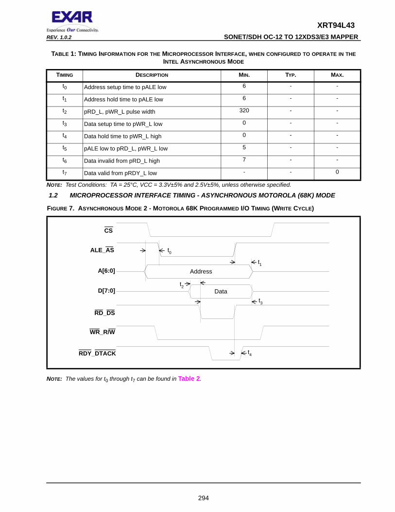
1.1 MICROPROCESSOR INTERFACE TIMING - ASYNCHRONOUS INTEL MODE.......................................... 293FIGURE 5. ASYNCHRONOUS MODE 1 - INTEL TYPE PROGRAMMED I/O TIMING (WRITE CYCLE) ....................................................... 293FIGURE 6. ASYNCHRONOUS MODE 1 - INTEL TYPE PROGRAMMED I/O TIMING (READ CYCLE)......................................................... 293TABLE 1: TIMING INFORMATION FOR THE MICROPROCESSOR INTERFACE, WHEN CONFIGURED TO OPERATE IN THE INTEL ASYNCHRONOUS
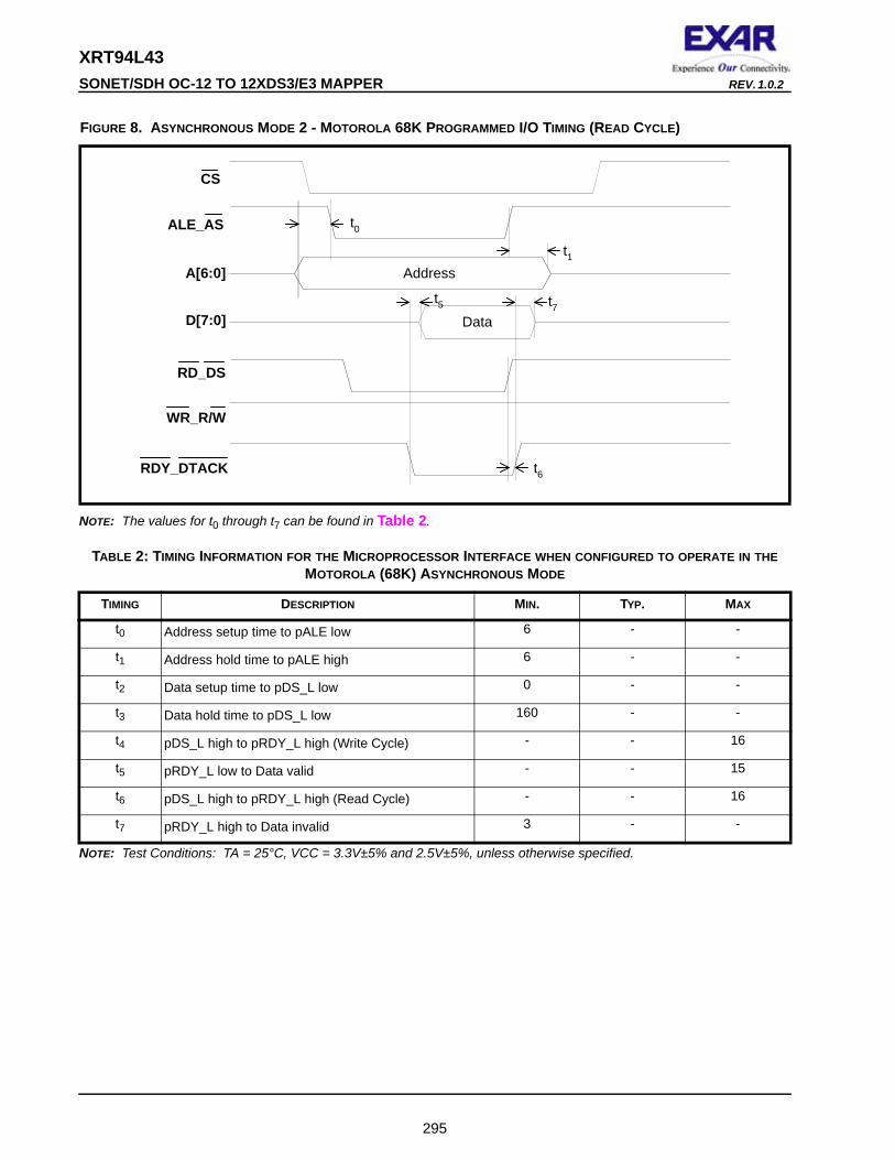
FIGURE 7. ASYNCHRONOUS MODE 2 - MOTOROLA 68K PROGRAMMED I/O TIMING (WRITE CYCLE) ................................................ 294FIGURE 8. ASYNCHRONOUS MODE 2 - MOTOROLA 68K PROGRAMMED I/O TIMING (READ CYCLE) ................................................. 295TABLE 2: TIMING INFORMATION FOR THE MICROPROCESSOR INTERFACE WHEN CONFIGURED TO OPERATE IN THE MOTOROLA (68K) ASYN-
CHRONOUS MODE ........................................................................................................................................................ 2951.3 MICROPROCESSOR INTERFACE TIMING - POWER PC 403 SYNCHRONOUS MODE ............................ 296
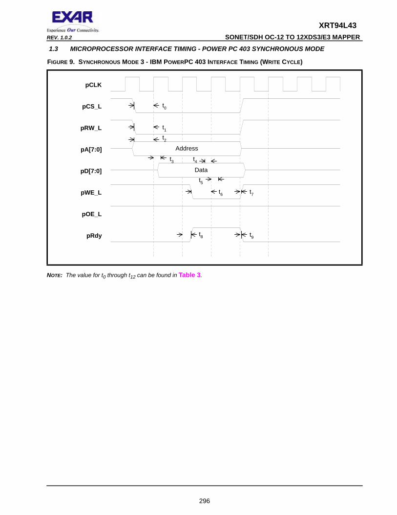
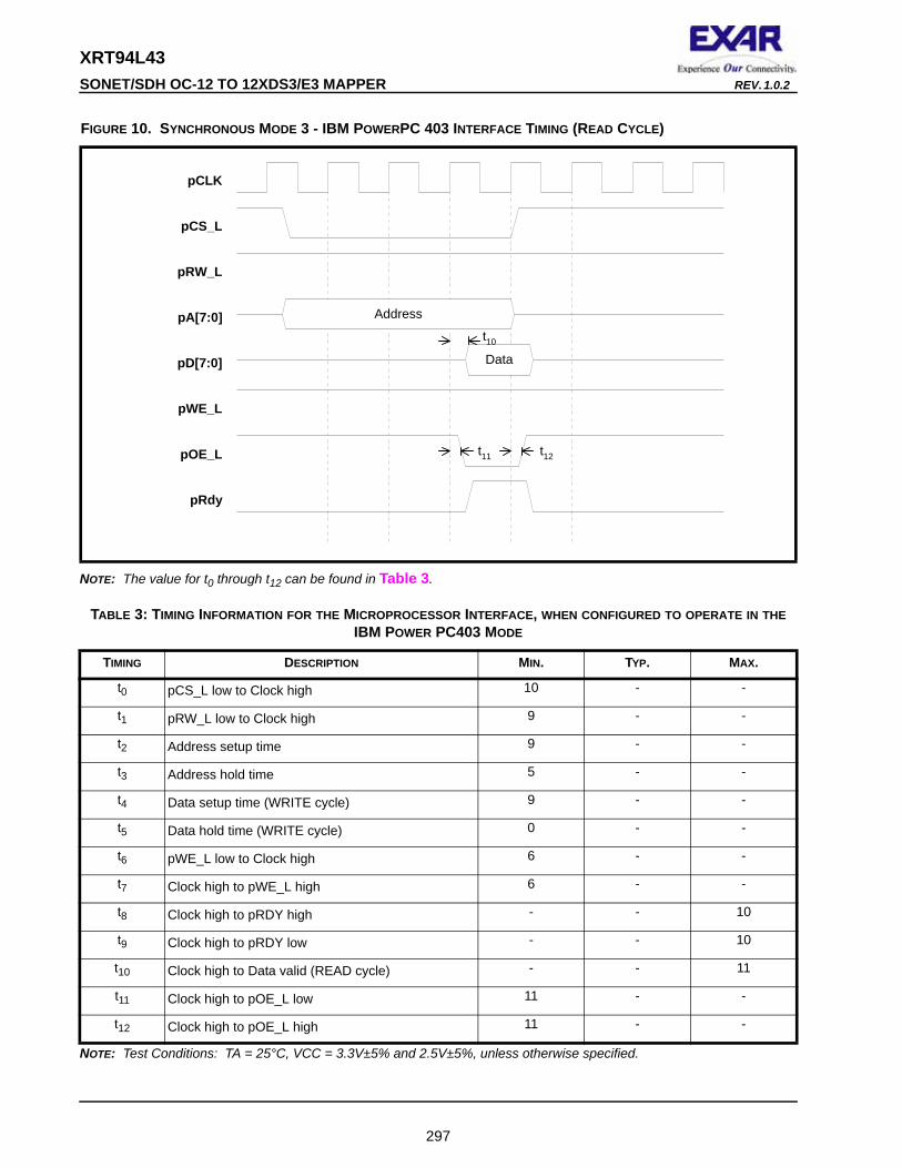
FIGURE 9. SYNCHRONOUS MODE 3 - IBM POWERPC 403 INTERFACE TIMING (WRITE CYCLE)....................................................... 296FIGURE 10. SYNCHRONOUS MODE 3 - IBM POWERPC 403 INTERFACE TIMING (READ CYCLE) ...................................................... 297TABLE 3: TIMING INFORMATION FOR THE MICROPROCESSOR INTERFACE, WHEN CONFIGURED TO OPERATE IN THE IBM POWER PC403 MODE
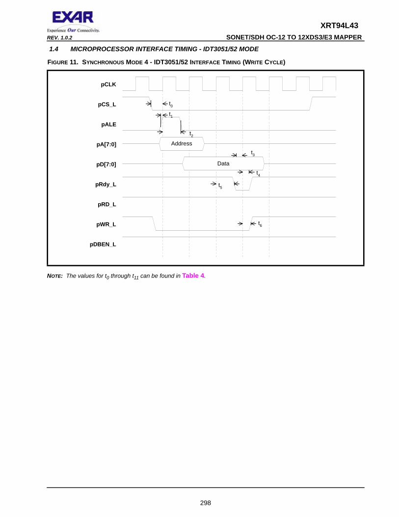
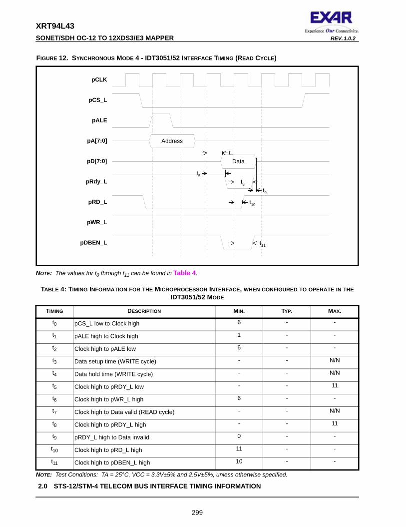
FIGURE 11. SYNCHRONOUS MODE 4 - IDT3051/52 INTERFACE TIMING (WRITE CYCLE)................................................................. 298FIGURE 12. SYNCHRONOUS MODE 4 - IDT3051/52 INTERFACE TIMING (READ CYCLE) .................................................................. 299TABLE 4: TIMING INFORMATION FOR THE MICROPROCESSOR INTERFACE, WHEN CONFIGURED TO OPERATE IN THE IDT3051/52 MODE 299
2.0 STS-12/STM-4 TELECOM BUS INTERFACE TIMING INFORMATION............................................. 2992.1 STS-12/STM-4 TELECOM BUS INTERFACE TIMING INFORMATION......................................................... 3002.2 THE TRANSMIT STS-12/STM-4 TELECOM BUS INTERFACE TIMING ....................................................... 300
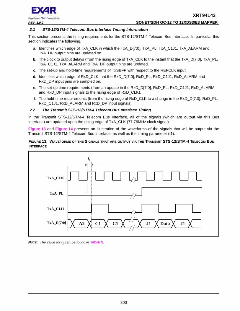
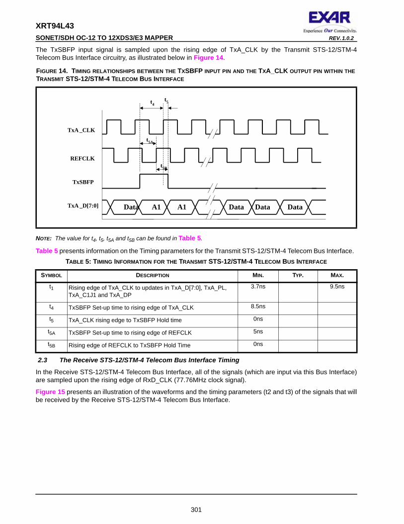
FIGURE 13. WAVEFORMS OF THE SIGNALS THAT ARE OUTPUT VIA THE TRANSMIT STS-12/STM-4 TELECOM BUS INTERFACE ......... 300FIGURE 14. TIMING RELATIONSHIPS BETWEEN THE TXSBFP INPUT PIN AND THE TXA_CLK OUTPUT PIN WITHIN THE TRANSMIT STS-12/STM-
4 TELECOM BUS INTERFACE ........................................................................................................................................ 301TABLE 5: TIMING INFORMATION FOR THE TRANSMIT STS-12/STM-4 TELECOM BUS INTERFACE ..................................................... 301
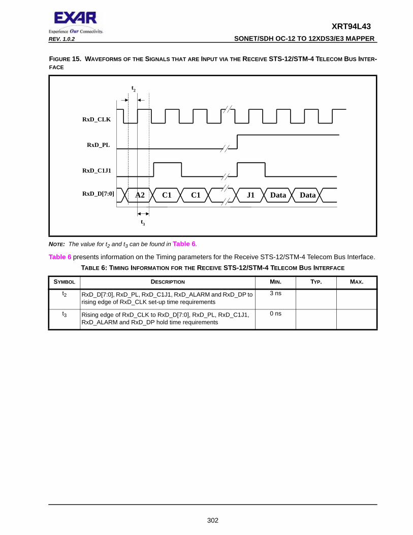
2.3 THE RECEIVE STS-12/STM-4 TELECOM BUS INTERFACE TIMING .......................................................... 301FIGURE 15. WAVEFORMS OF THE SIGNALS THAT ARE INPUT VIA THE RECEIVE STS-12/STM-4 TELECOM BUS INTERFACE .............. 302TABLE 6: TIMING INFORMATION FOR THE RECEIVE STS-12/STM-4 TELECOM BUS INTERFACE ....................................................... 302
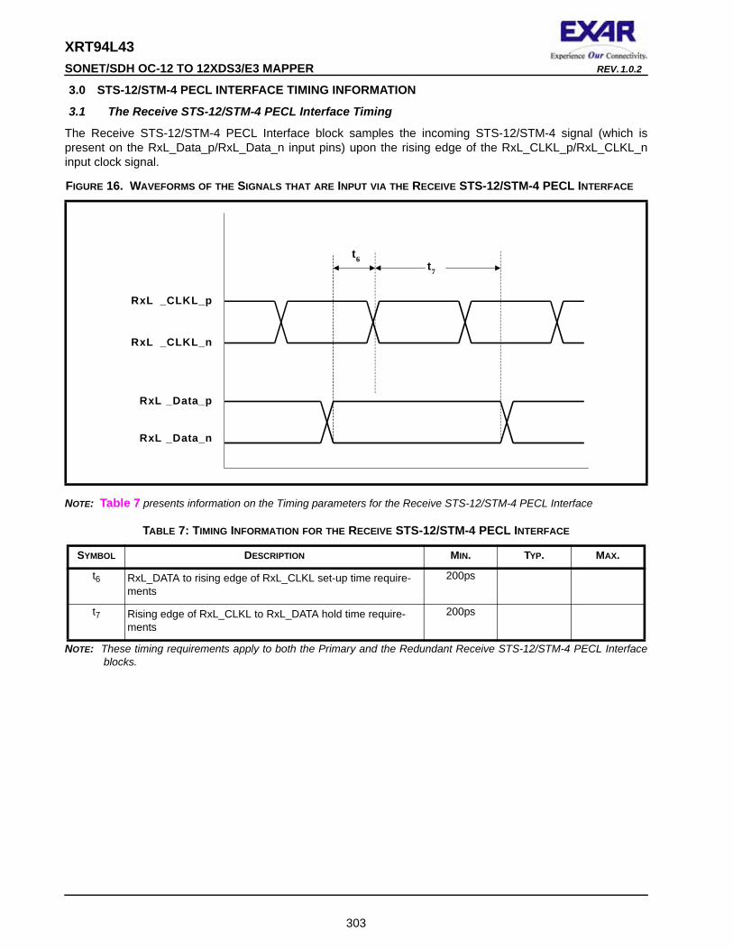
3.0 STS-12/STM-4 PECL INTERFACE TIMING INFORMATION ............................................................. 3033.1 THE RECEIVE STS-12/STM-4 PECL INTERFACE TIMING........................................................................... 303
FIGURE 16. WAVEFORMS OF THE SIGNALS THAT ARE INPUT VIA THE RECEIVE STS-12/STM-4 PECL INTERFACE........................... 303TABLE 7: TIMING INFORMATION FOR THE RECEIVE STS-12/STM-4 PECL INTERFACE ................................................................... 303
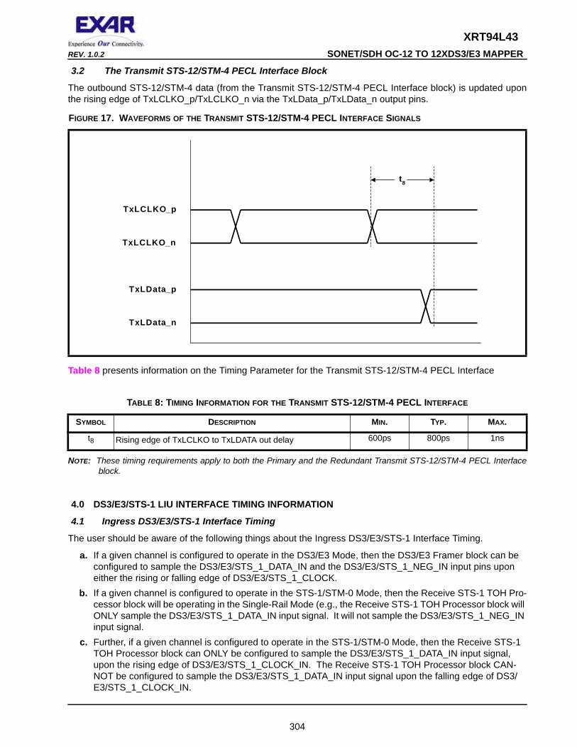
3.2 THE TRANSMIT STS-12/STM-4 PECL INTERFACE BLOCK....................................................................... 304FIGURE 17. WAVEFORMS OF THE TRANSMIT STS-12/STM-4 PECL INTERFACE SIGNALS .............................................................. 304TABLE 8: TIMING INFORMATION FOR THE TRANSMIT STS-12/STM-4 PECL INTERFACE ................................................................. 304
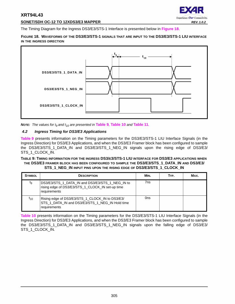
FIGURE 18. WAVEFORMS OF THE DS3/E3/STS-1 SIGNALS THAT ARE INPUT TO THE DS3/E3/STS-1 LIU INTERFACE IN THE INGRESS DIREC-TION ........................................................................................................................................................................... 305
4.2 INGRESS TIMING FOR DS3/E3 APPLICATIONS.......................................................................................... 305TABLE 9: TIMING INFORMATION FOR THE INGRESS DS3/E3/STS-1 LIU INTERFACE FOR DS3/E3 APPLICATIONS WHEN THE DS3/E3 FRAMER
BLOCK HAS BEEN CONFIGURED TO SAMPLE THE DS3/E3/STS_1_DATA_IN AND DS3/E3/STS_1_NEG_IN INPUT PINS UPON THE RISING EDGE OF DS3/E3/STS_1_CLOCK_IN ............................................................................................................ 305
TABLE 10: TIMING INFORMATION FOR THE INGRESS DS3/E3/STS-1 LIU INTERFACE FOR DS3/E3 APPLICATIONS AND WHEN THE DS3/E3 FRAMER BLOCK HAS BEEN CONFIGURED TO SAMPLE THE DS3/E3/STS_1_DATA_IN AND DS3/E3/STS_1_NEG_IN INPUT PINS UPON THE FALLING EDGE OF DS3/E3/STS_1_CLOCK_IN ........................................................................................... 306
4.3 INGRESS TIMING FOR STS-1/STM-0 APPLICATIONS ................................................................................ 306TABLE 11: TIMING INFORMATION FOR THE INGRESS DS3/E3/STS-1 LIU INTERFACE FOR STS-1/STM-0 APPLICATIONS ................. 306
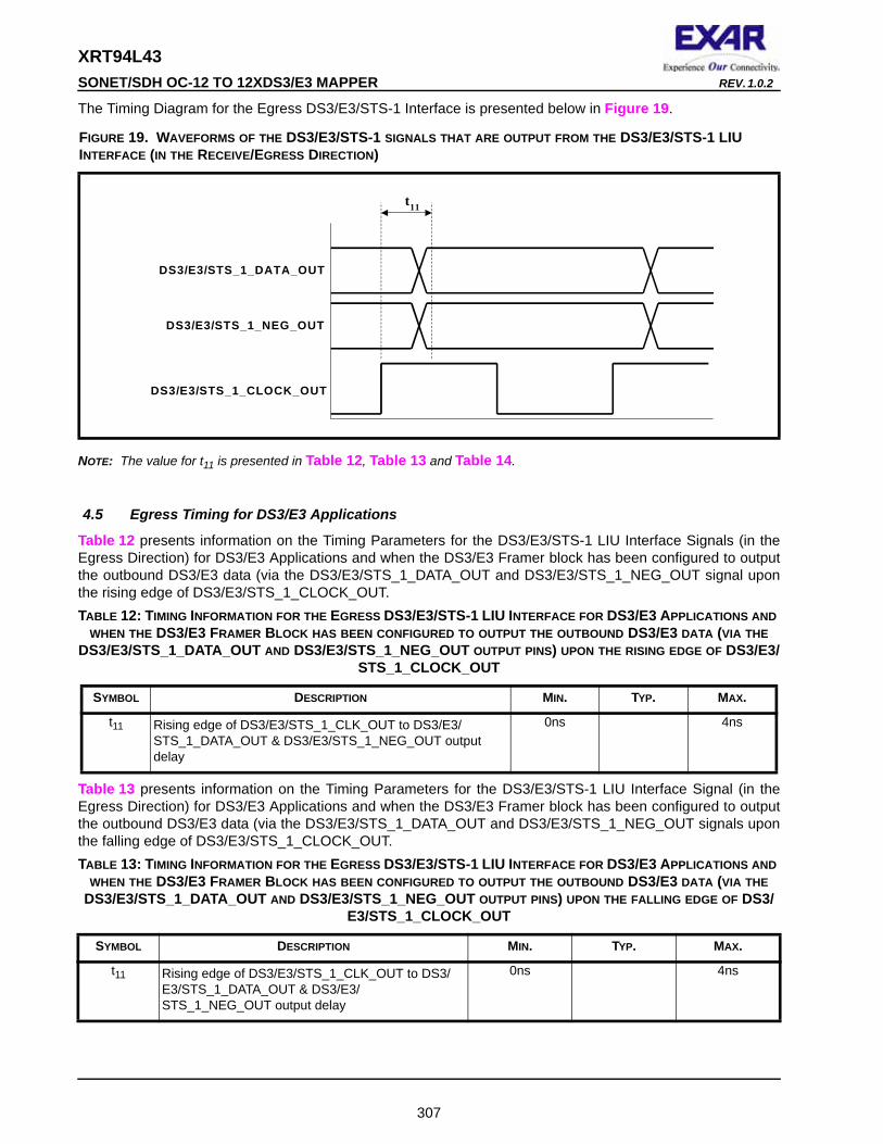
4.4 THE EGRESS DS3/E3/STS-1 INTERFACE TIMING....................................................................................... 306FIGURE 19. WAVEFORMS OF THE DS3/E3/STS-1 SIGNALS THAT ARE OUTPUT FROM THE DS3/E3/STS-1 LIU INTERFACE (IN THE RECEIVE/
XRT94L43 SONET/SDH OC-12 TO 12XDS3/E3 MAPPER REV. 1.0.2
4.5 EGRESS TIMING FOR DS3/E3 APPLICATIONS ........................................................................................... 307TABLE 12: TIMING INFORMATION FOR THE EGRESS DS3/E3/STS-1 LIU INTERFACE FOR DS3/E3 APPLICATIONS AND WHEN THE DS3/E3
FRAMER BLOCK HAS BEEN CONFIGURED TO OUTPUT THE OUTBOUND DS3/E3 DATA (VIA THE DS3/E3/STS_1_DATA_OUT AND DS3/E3/STS_1_NEG_OUT OUTPUT PINS) UPON THE RISING EDGE OF DS3/E3/STS_1_CLOCK_OUT ....................... 307
TABLE 13: TIMING INFORMATION FOR THE EGRESS DS3/E3/STS-1 LIU INTERFACE FOR DS3/E3 APPLICATIONS AND WHEN THE DS3/E3 FRAMER BLOCK HAS BEEN CONFIGURED TO OUTPUT THE OUTBOUND DS3/E3 DATA (VIA THE DS3/E3/STS_1_DATA_OUT AND DS3/E3/STS_1_NEG_OUT OUTPUT PINS) UPON THE FALLING EDGE OF DS3/E3/STS_1_CLOCK_OUT ..................... 307
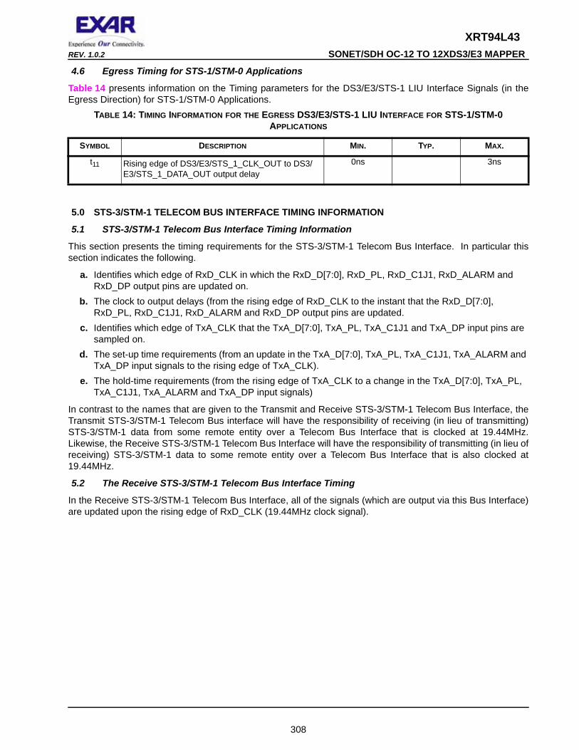
4.6 EGRESS TIMING FOR STS-1/STM-0 APPLICATIONS.................................................................................. 308TABLE 14: TIMING INFORMATION FOR THE EGRESS DS3/E3/STS-1 LIU INTERFACE FOR STS-1/STM-0 APPLICATIONS .................. 308
5.0 STS-3/STM-1 TELECOM BUS INTERFACE TIMING INFORMATION ............................................... 3085.1 STS-3/STM-1 TELECOM BUS INTERFACE TIMING INFORMATION........................................................... 3085.2 THE RECEIVE STS-3/STM-1 TELECOM BUS INTERFACE TIMING ............................................................ 308
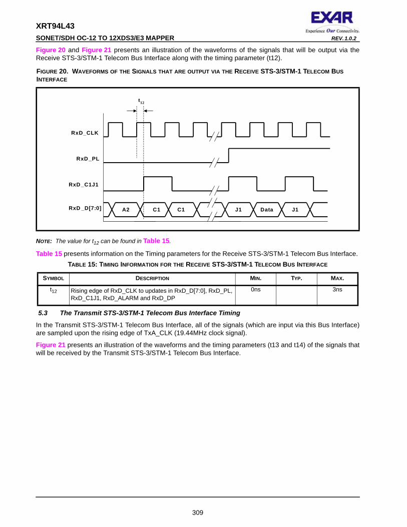
FIGURE 20. WAVEFORMS OF THE SIGNALS THAT ARE OUTPUT VIA THE RECEIVE STS-3/STM-1 TELECOM BUS INTERFACE ............. 309TABLE 15: TIMING INFORMATION FOR THE RECEIVE STS-3/STM-1 TELECOM BUS INTERFACE ....................................................... 309
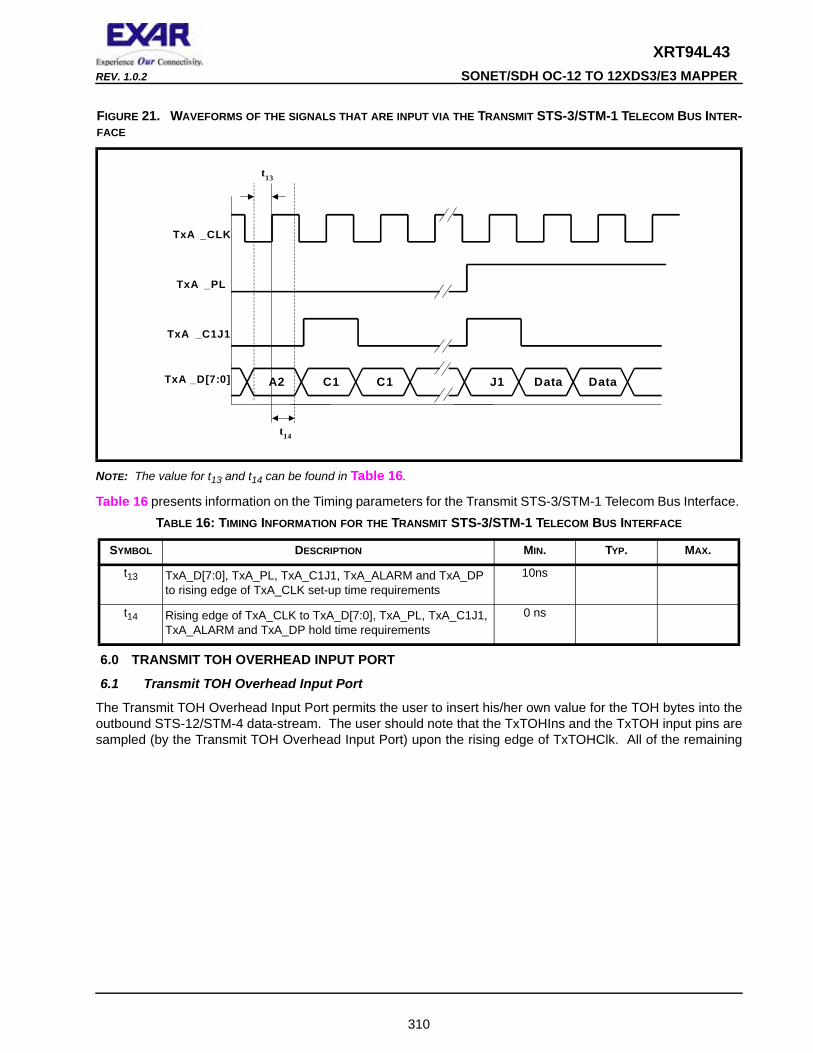
5.3 THE TRANSMIT STS-3/STM-1 TELECOM BUS INTERFACE TIMING.......................................................... 309FIGURE 21. WAVEFORMS OF THE SIGNALS THAT ARE INPUT VIA THE TRANSMIT STS-3/STM-1 TELECOM BUS INTERFACE.............. 310TABLE 16: TIMING INFORMATION FOR THE TRANSMIT STS-3/STM-1 TELECOM BUS INTERFACE ..................................................... 310
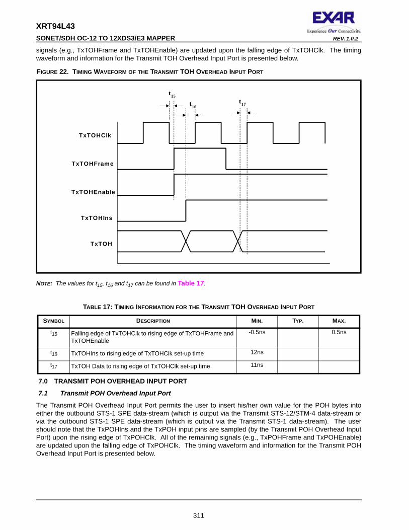
FIGURE 22. TIMING WAVEFORM OF THE TRANSMIT TOH OVERHEAD INPUT PORT.......................................................................... 311TABLE 17: TIMING INFORMATION FOR THE TRANSMIT TOH OVERHEAD INPUT PORT ....................................................................... 311
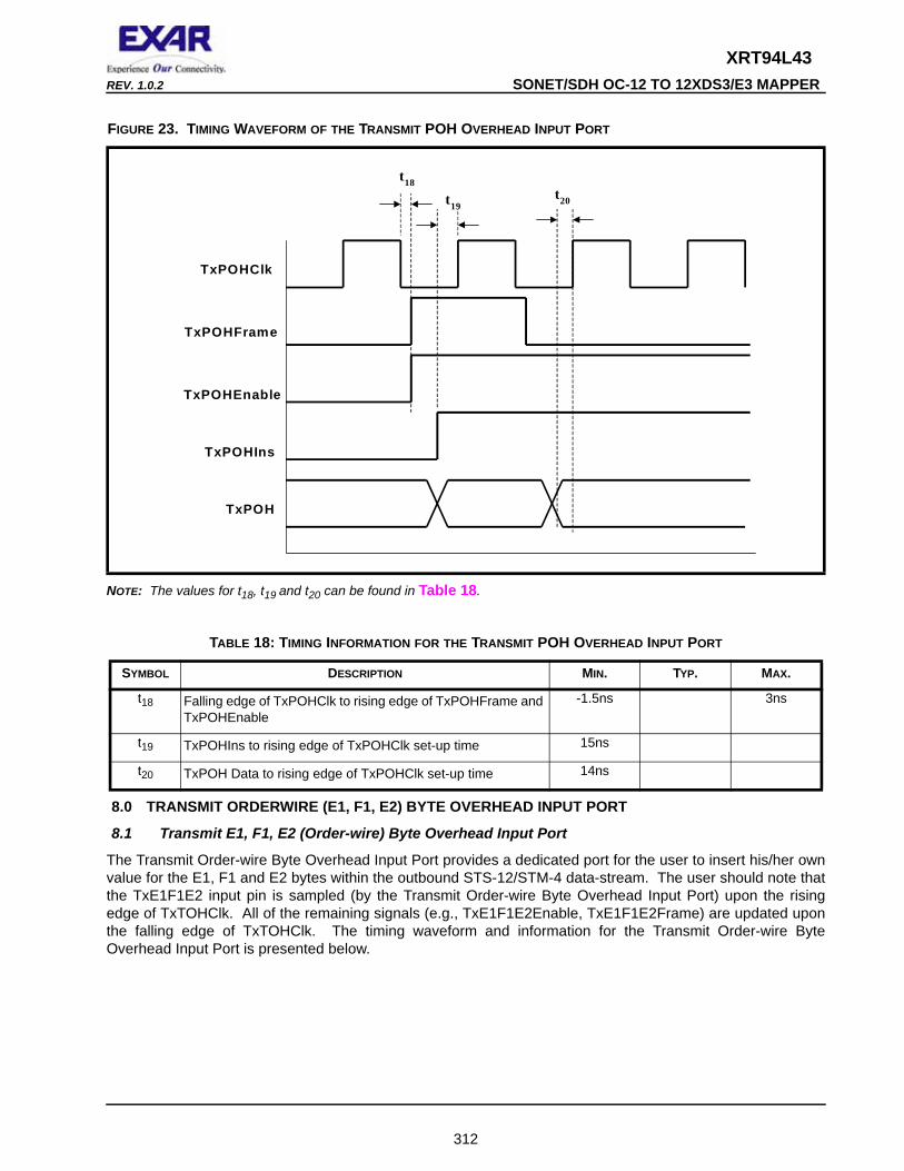
FIGURE 23. TIMING WAVEFORM OF THE TRANSMIT POH OVERHEAD INPUT PORT.......................................................................... 312TABLE 18: TIMING INFORMATION FOR THE TRANSMIT POH OVERHEAD INPUT PORT ....................................................................... 312
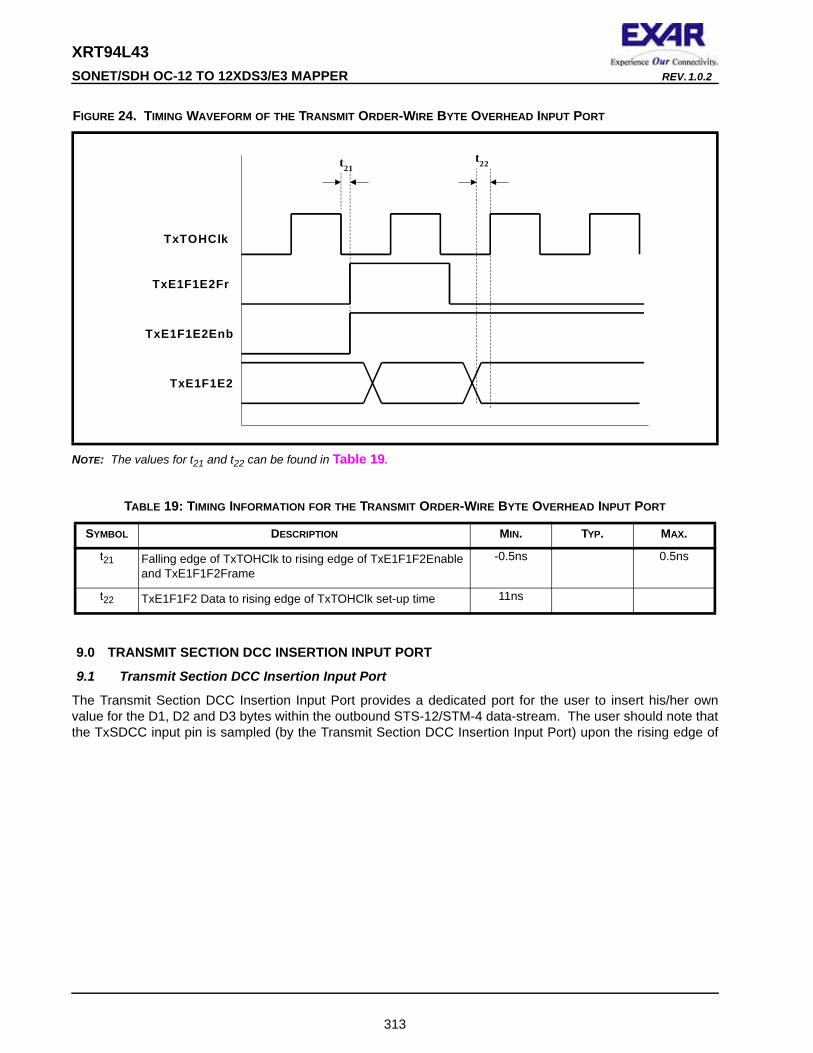
FIGURE 24. TIMING WAVEFORM OF THE TRANSMIT ORDER-WIRE BYTE OVERHEAD INPUT PORT .................................................... 313TABLE 19: TIMING INFORMATION FOR THE TRANSMIT ORDER-WIRE BYTE OVERHEAD INPUT PORT ................................................. 313
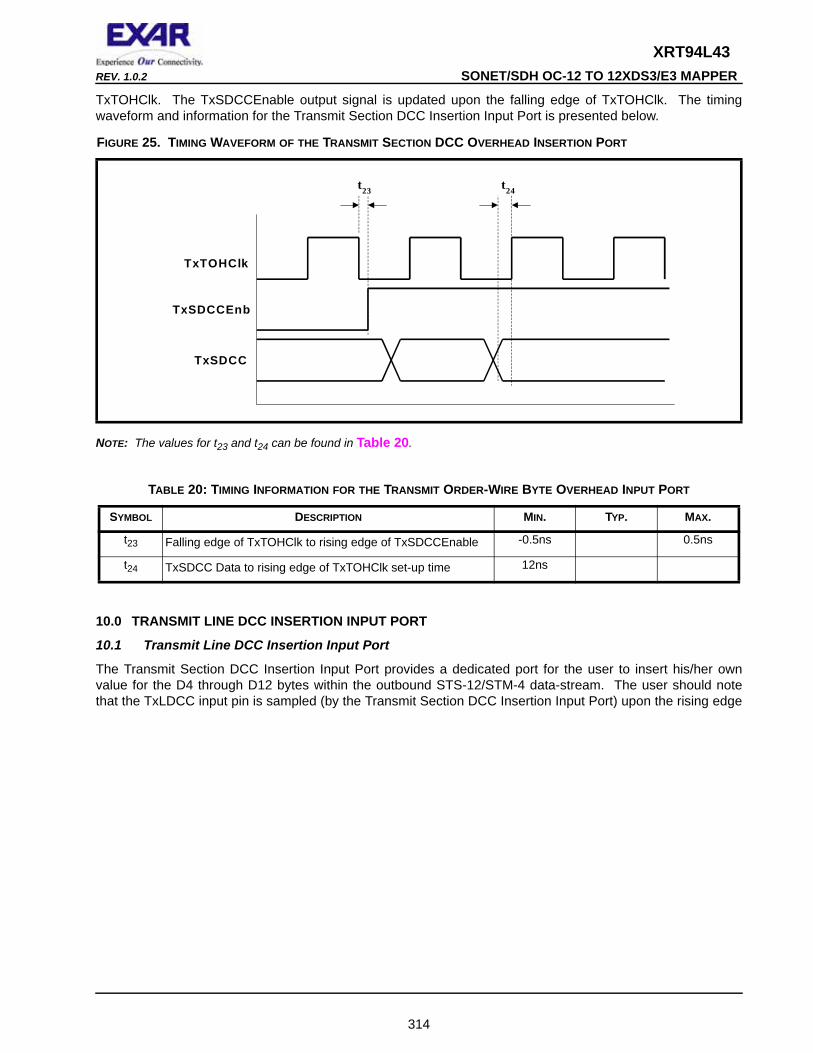
FIGURE 25. TIMING WAVEFORM OF THE TRANSMIT SECTION DCC OVERHEAD INSERTION PORT .................................................... 314TABLE 20: TIMING INFORMATION FOR THE TRANSMIT ORDER-WIRE BYTE OVERHEAD INPUT PORT ................................................. 314
10.0 TRANSMIT LINE DCC INSERTION INPUT PORT ............................................................................ 31410.1 TRANSMIT LINE DCC INSERTION INPUT PORT........................................................................................ 314
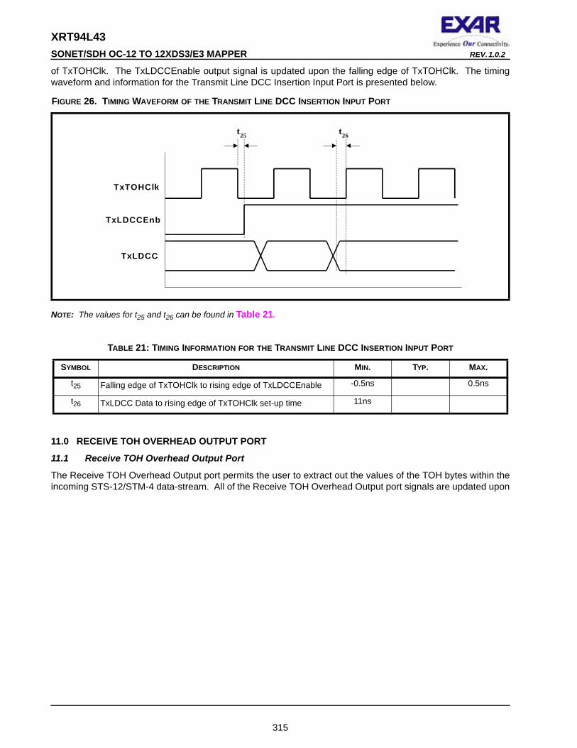
FIGURE 26. TIMING WAVEFORM OF THE TRANSMIT LINE DCC INSERTION INPUT PORT................................................................... 315TABLE 21: TIMING INFORMATION FOR THE TRANSMIT LINE DCC INSERTION INPUT PORT ................................................................ 315
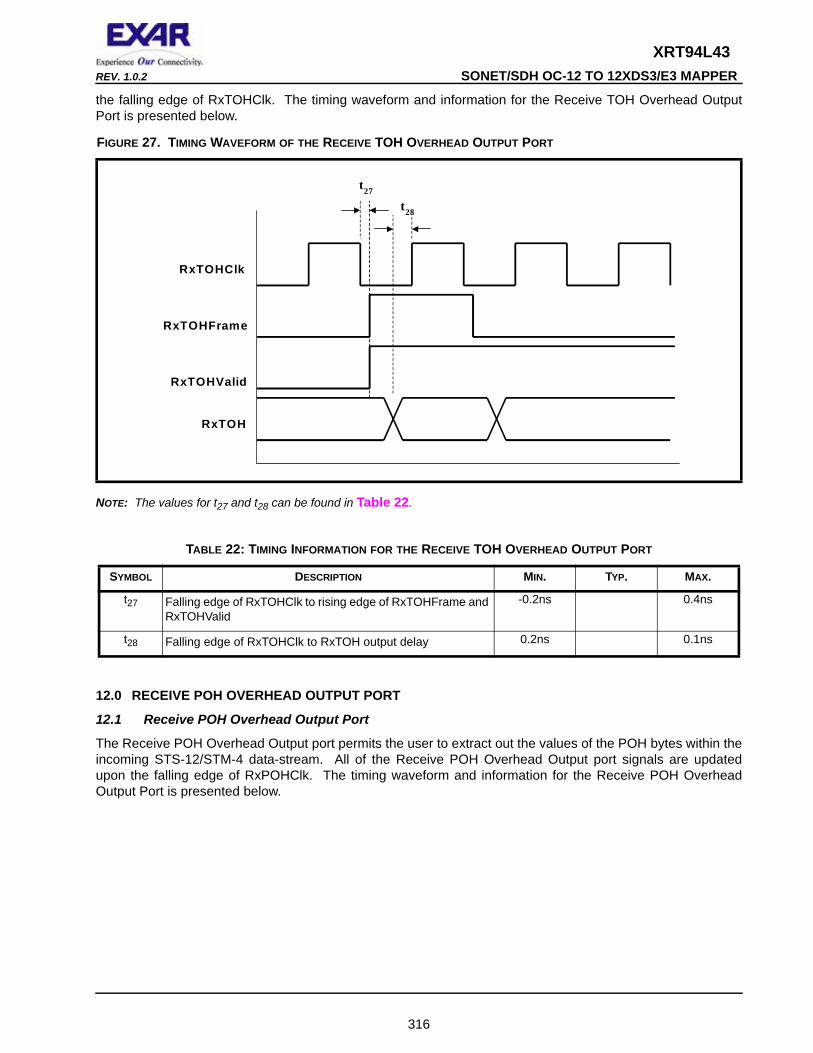
FIGURE 27. TIMING WAVEFORM OF THE RECEIVE TOH OVERHEAD OUTPUT PORT ........................................................................ 316TABLE 22: TIMING INFORMATION FOR THE RECEIVE TOH OVERHEAD OUTPUT PORT ..................................................................... 316
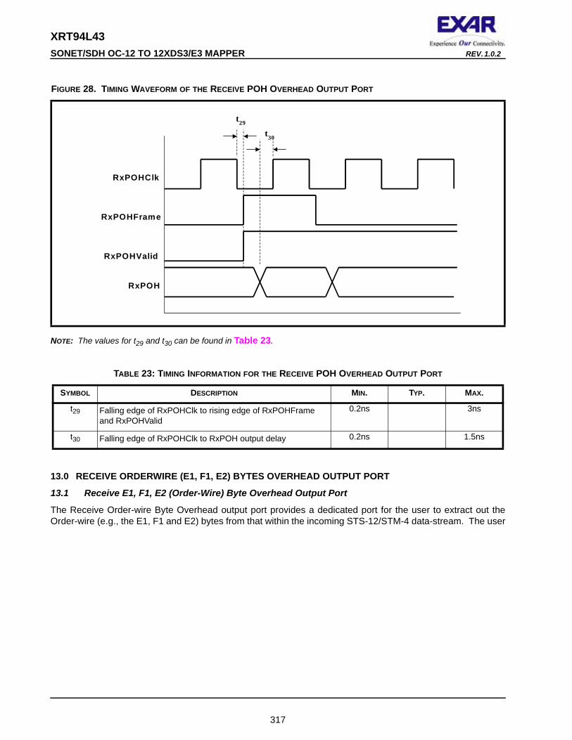
FIGURE 28. TIMING WAVEFORM OF THE RECEIVE POH OVERHEAD OUTPUT PORT ........................................................................ 317TABLE 23: TIMING INFORMATION FOR THE RECEIVE POH OVERHEAD OUTPUT PORT ..................................................................... 317
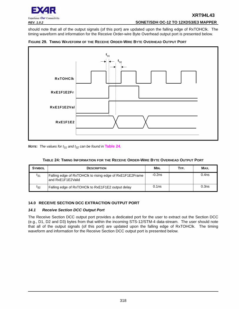
FIGURE 29. TIMING WAVEFORM OF THE RECEIVE ORDER-WIRE BYTE OVERHEAD OUTPUT PORT................................................... 318TABLE 24: TIMING INFORMATION FOR THE RECEIVE ORDER-WIRE BYTE OVERHEAD OUTPUT PORT ................................................ 318
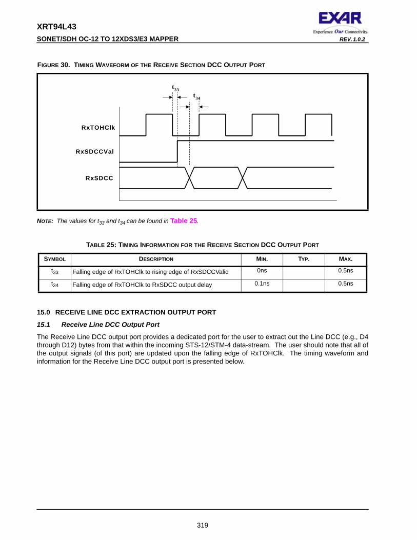
14.0 RECEIVE SECTION DCC EXTRACTION OUTPUT PORT ............................................................... 31814.1 RECEIVE SECTION DCC OUTPUT PORT ................................................................................................... 318
FIGURE 30. TIMING WAVEFORM OF THE RECEIVE SECTION DCC OUTPUT PORT............................................................................ 319TABLE 25: TIMING INFORMATION FOR THE RECEIVE SECTION DCC OUTPUT PORT ......................................................................... 319
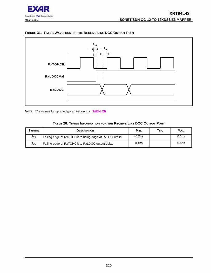
15.0 RECEIVE LINE DCC EXTRACTION OUTPUT PORT ....................................................................... 31915.1 RECEIVE LINE DCC OUTPUT PORT ........................................................................................................... 319
FIGURE 31. TIMING WAVEFORM OF THE RECEIVE LINE DCC OUTPUT PORT .................................................................................. 320TABLE 26: TIMING INFORMATION FOR THE RECEIVE LINE DCC OUTPUT PORT ............................................................................... 320
XRT94L43REV. 1.0.2 SONET/SDH OC-12 TO 12XDS3/E3 MAPPER
8
PIN DESCRIPTIONS - DIRECT ADDRESSING MICROPROCESSOR INTERFACE
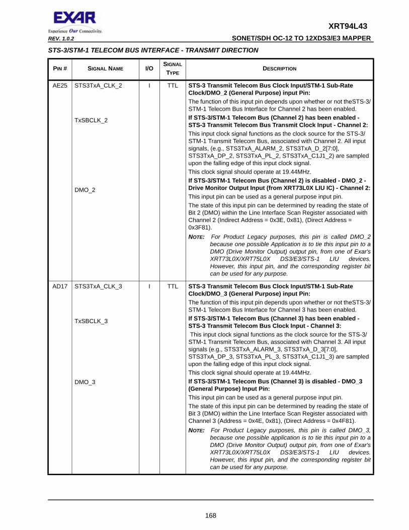
PIN # SIGNAL NAME I/OSIGNAL
TYPEDESCRIPTION
U22 PCLK I TTL Microprocessor Interface Clock Input:This clock input signal is only used if the Microprocessor Interface has been configured to operate in one of the Synchronous Modes (e.g., Power PC 403 Mode). If the Microprocessor Interface is configured to operate in one of these modes, then it will use this clock signal to do the following.• To sample the CS, WR/R/W, A[15:0], D[7:0], RD/DS and DBEN input
pins, and• To update the state of the D[7:0] and the RDY/DTACK output signals.NOTES:
1. The Microprocessor Interface can work with µPCLK frequencies ranging up to 66MHz.
2. This pin is inactive if the user has configured the Microprocessor Interface to operate in either the Intel-Asynchronous or the Motorola-Asynchronous Modes. In this case, the user should tie this pin to GND.
L25L23L22
PTYPE_0PTYPE_1PTYPE_2
I TTL Microprocessor Type Select input:These three input pins are used to configure the Microprocessor Interface block to readily support a wide variety of Microprocessor Interfaces. The relationship between the settings of these input pins and the corresponding Microprocessor Interface configuration is presented below.PTYPE[2:0] Microprocessor Interface Mode 000 Intel - Asynchronous Mode l001 Motorola - Asynchronous Mode (Motorola 68k) 010 Intel X86 011 Intel I960 100 IDT3051/52 (MIPS) 101 Power PC 403 Mode
I TTL Address Bus Input pins (Microprocessor Interface):These pins permit the Microprocessor to identify on-chip registers and Buffer/Memory locations (within the XRT94L43) whenever it performs READ and WRITE operations with the XRT94L43.
XRT94L43 SONET/SDH OC-12 TO 12XDS3/E3 MAPPER REV. 1.0.2
I/O TTL Bi-Directional Data Bus Pins (Microprocessor Interface):These pins are used to drive and receive data over the bi-directional data bus,, whenever the Microprocessor performs READ or WRITE operations with the Microprocessor Interface of the XRT94L43.
Y26 WR/R/W
I TTL Write Strobe/Read-Write operation Identifier:The function of this input pin depends upon which mode the Microproces-sor Interface has been configured to operate in.Intel-Asynchronous Mode - WR - Write Strobe Input:If the Microprocessor Interface is configured to operate in the Intel-Asyn-chronous Mode, then this input pin functions as the WR (Active Low WRITE Strobe) input signal from the Microprocessor. Once this active-low signal is asserted, then the input buffers (associated with the Bi-Directional Data Bus pin, D[7:0]) will be enabled. The Microprocessor Interface will latch the contents on the Bi-Directional Data Bus (into the "target" register or address location, within the XRT94L43) upon the rising edge of this input pin.Motorola-Asynchronous Mode - R/W - Read/Write Operation Identifi-cation Input Pin:If the Microprocessor Interface is operating in the "Motorola-Asynchronous Mode", then this pin is functionally equivalent to the "R/W" input pin. In the Motorola Mode, a "READ" operation occurs if this pin is held at a logic "1", coincident to a falling edge of the RD/DS (Data Strobe) input pin. Similarly a WRITE operation occurs if this pin is at a logic "0", coincident to a falling edge of the RD/DS (Data Strobe) input pin.Power PC 403 Mode - R/W - Read/Write Operation Identification Input:If the Microprocessor Interface is configured to operate in the Power PC 403 Mode, then this input pin will function as the "Read/Write Operation Identification Input" pin.Anytime the Microprocessor Interface samples this input signal at a logic low (while also sampling the CS input pin "low") upon the rising edge of µPCLK, then the Microprocessor Interface will (upon the very same rising edge of µPCLK) latch the contents of the Address Bus (A[15:0]) into the Microprocessor Interface circuitry, in preparation for this forthcoming READ operation. At some point (later in this READ operation) the Microprocessor will also assert the DBEN/OE input pin, and the Microprocessor Interface will then place the contents of the "target" register (or address location within the XRT94L43) upon the Bi-Directional Data Bus pins (D[7:0]), where it can be read by the Microprocessor .Anytime the Microprocessor Interface samples this input signal at a logic high (while also sampling the CS input pin a logic "low") upon the rising edge of µPCLK, then the Microprocessor Interface will (upon the very same rising edge of µPCLK) latch the contents of the Address Bus (A[15:0]) into the Microprocessor Interface circuitry, in preparation for the forthcoming WRITE operation. At some point (later in this WRITE operation) the Micro-processor will also assert the RD/DS/WE input pin, and the Microprocessor Interface will then latch the contents of the Bi-Directional Data Bus (D[7:0]) into the contents of the "target" register or buffer location (within the XRT94L43).
MICROPROCESSOR INTERFACE
PIN # SIGNAL NAME I/OSIGNAL
TYPEDESCRIPTION
XRT94L43REV. 1.0.2 SONET/SDH OC-12 TO 12XDS3/E3 MAPPER
10
T23 RD/DS/WE
I TTL READ Strob/Data Strobe:The function of this input pin depends upon which mode the Microproces-sor Interface has been configured to operate in.Intel-Asynchronous Mode - RD - READ Strobe Input:If the Microprocessor Interface is operating in the Intel-Asynchronous Mode, then this input pin will function as the RD (Active Low Read Strobe) input signal from the Microprocessor. Once this active-low signal is asserted, then the XRT94L43 will place the contents of the addressed reg-ister (or buffer location) on the Microprocessor Interface Bi-directional data bus (D[7:0]). When this signal is negated, then the Data Bus will be tri-stated.Motorola-Asynchronous (68K) Mode - DS - Data Strobe:If the Microprocessor Interface is operating in the Motorola-Asynchronous Mode, then this input pin will function as the DS (Data Strobe) input signal. Power PC 403 Mode - WE - Write Enable Input:If the Microprocessor Interface is operating in the Power PC 403 Mode, then this input pin will function as the WE (Write Enable) input pin. Anytime the Microprocessor Interface samples this active-low input signal (along with CS and WR/R/W) also being asserted (at a logic low level) upon the rising edge of µPCLK, then the Microprocessor Interface will (upon the very same rising edge of µPCLK) latch the contents on the Bi-Directional Data Bus (D[7:0]) into the "target" on-chip register or buffer location within the XRT94L43.
R23 PALE/PAS_L I TTL Address Latch Enable/Address Strobe:This input pin is used to latch the address (present at the Microprocessor Interface Address Bus pins (A[6:0]) into the Mapper/Framer Microprocessor Interface block and to indicate the start of a READ or WRITE cycle. This input pin is active-High, in the Intel Mode and active-Low in the Motorola Mode.
V22 PCS_L I TTL Chip Select Input:The user must assert this active low signal in order to select the Micropro-cessor Interface for READ and WRITE operations between the Micropro-cessor and the XRT94L43 on-chip registers and buffer locations.
MICROPROCESSOR INTERFACE
PIN # SIGNAL NAME I/OSIGNAL
TYPEDESCRIPTION
XRT94L43 SONET/SDH OC-12 TO 12XDS3/E3 MAPPER REV. 1.0.2
Y25 PRDY_L/DTACK/RDY
O CMOS READY or DTACK Output:The function of this input pin depends upon which mode the Microproces-sor Interface has been configured to operate in.Intel-Asynchronous Mode - RDY - Ready Output:If the Microprocessor Interface has been configured to operate in the Intel-Asynchronous Mode, then this output pin will function as the "active-low" READY output.During a READ or WRITE cycle, the Microprocessor Interface block will toggle this output pin to the logic low level, ONLY when it (the Microproces-sor Interface) is ready to complete or terminate the current READ or WRITE cycle. Once the Microprocessor has determined that this input pin has toggled to the logic "low" level, then it is now safe for it to move on and execute the next READ or WRITE cycle. If (during a READ or WRITE cycle) the Microprocessor Interface block is holding this output pin at a logic "high" level, then the Microprocessor is expected to extend this READ or WRITE cycle, until it detects this output pin being toggled to the logic low level.Motorola-Asynchronous Mode - DTACK - Data Transfer Acknowledge Output If the Microprocessor Interface has been configured to operate in the Motorola-Asynchronous Mode, then this output pin will function as the "active-low" DTACK output.During a READ or WRITE cycle, the Microprocessor Interface block will toggle this output pin to the logic low level, ONLY when it (the Microproces-sor Interface) is ready to complete or terminate the current READ or WRITE cycle. Once the Microprocessor has determined that this input pin has toggled to the logic "low" level, then it is now safe for it to move on and execute the next READ or WRITE cycle. If (during a READ or WRITE cycle) the Microprocessor Interface block is holding this output pin at a logic "high" level, then the Microprocessor is expected to extend this READ or WRITE cycle, until it detects this output pin being toggled to the logic low level.Power PC 403 Mode - RDY - Ready Output:If the Microprocessor Interface has been configured to operate in the Power PC 403 Mode, then this output pin will function as the "active-high" READY output.During a READ or WRITE cycle, the Microprocessor Interface block will toggle this output pin to the logic high level, ONLY when it (the Micro-processor Interface) is ready to complete or terminate the current READ or WRITE cycle. Once the Microprocessor has sampled this signal being at the logic "high" level (upon the rising edge of PCLK), then it is now safe for it to move on and execute the next READ or WRITE cycle. If (during a READ or WRITE cycle) the Microprocessor Interface block is holding this output pin at a logic "low" level, then the Microprocessor is expected to extend this READ or WRITE cycle, until it samples this output pin being at the logic low level.NOTE: The Microprocessor Interface will update the state of this output pin
upon the rising edge of µPCLK.
MICROPROCESSOR INTERFACE
PIN # SIGNAL NAME I/OSIGNAL
TYPEDESCRIPTION
11
XRT94L43REV. 1.0.2 SONET/SDH OC-12 TO 12XDS3/E3 MAPPER
T21 PDBEN_L I TTL Bi-directional Data Bus Enable Input Pin:This input pin permits the user to either enable or tri-state the Bi-Directional Data Bus pins (D[7:0]), as described below. Setting this input pin "low" enables the Bi-directional Data bus. Setting this input "high" tri-states the Bi-directional Data Bus.
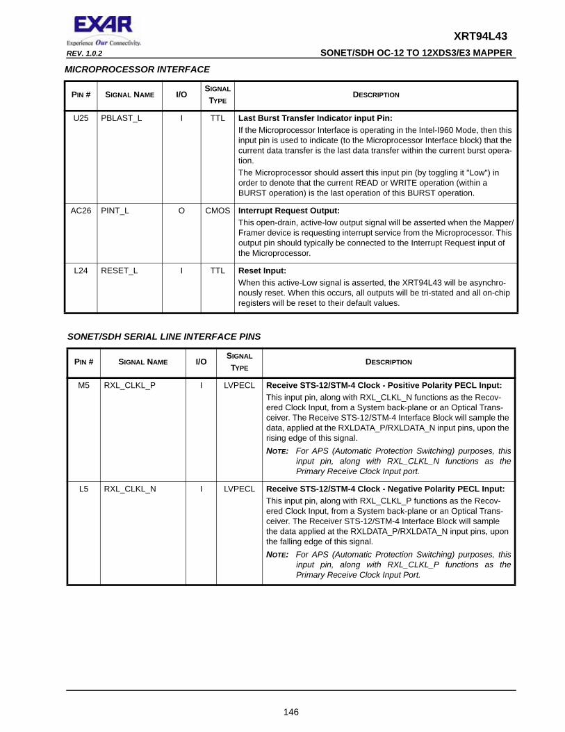
U25 PBLAST_L I TTL Last Burst Transfer Indicator input Pin:If the Microprocessor Interface is operating in the Intel-I960 Mode, then this input pin is used to indicate (to the Microprocessor Interface block) that the current data transfer is the last data transfer within the current burst opera-tion.The Microprocessor should assert this input pin (by toggling it "Low") in order to denote that the current READ or WRITE operation (within a BURST operation) is the last operation of this BURST operation.NOTE: If the user has configured the Microprocessor Interface to operate
in the Intel-Asynchronous, the Motorola-Asynchronous or the Power PC 403 Mode, then he/she should tie this input pin to GND.
AC26 PINT_L O CMOS Interrupt Request Output:This active-Low, active-low output signal will be asserted when the XRT94L43 is requesting interrupt service from the Microprocessor. This output pin should typically be connected to the Interrupt Request input of the Microprocessor.
L24 RESET_L I TTL Reset Input:When this active-Low signal is asserted, the XRT94L43 will be asynchro-nously reset. When this occurs, all outputs will be tri-stated and all on-chip registers will be reset to their default values.
M26 FULL_ADDR_SEL
I TTL Full Address Select input pin:This input pin, along with "DIRECT_ADD_SEL" (pin M23) must both be pulled "HIGH" in order to configure the Microprocessor Interface block to operate in the "Full Address" Mode.If the Microprocessor Interface is configured to operate in the "Full Address" Mode, then it will then provide a 16-bit Address Bus (which is sufficient to "Directly Address" all of the on-chip registers.
M23 DIRECT_ADD_SEL
I TTL Direct Address Select input pin:This input pin, along with "FULL_ADDR_SEL" (pin M26) must both be pulled "HIGH" in order to con-figure the Microprocessor Interface block to operate in the "Full Address" Mode.If the Microprocessor Interface is configured to operate in the "Full Address" Mode, then it will then provide a 16-bit Address Bus (which is suf-ficient to "Directly Address" all of the on-chip registers.
MICROPROCESSOR INTERFACE
PIN # SIGNAL NAME I/OSIGNAL
TYPEDESCRIPTION
12
XRT94L43 SONET/SDH OC-12 TO 12XDS3/E3 MAPPER REV. 1.0.2
13
SONET/SDH SERIAL LINE INTERFACE PINS
PIN # SIGNAL NAME I/OSIGNAL
TYPEDESCRIPTION
M5 RXL_CLKL_P I LVPECL Receive STS-12/STM-4 Clock - Positive Polarity PECL Input:This input pin, along with RXL_CLKL_N functions as the Recov-ered Clock Input, from a System back-plane or an Optical Trans-ceiver. The Receive STS-12/STM-4 Interface Block will sample the data, applied at the RXLDATA_P/RXLDATA_N input pins, upon the rising edge of this signal.NOTE: For APS (Automatic Protection Switching) purposes, this
input pin, along with RXL_CLKL_N functions as the Primary Receive Clock Input port.
L5 RXL_CLKL_N I LVPECL Receive STS-12/STM-4 Clock - Negative Polarity PECL Input:This input pin, along with RXL_CLKL_P functions as the Recov-ered Clock Input, from a System back-plane or an Optical Trans-ceiver. The Receiver STS-12/STM-4 Interface Block will sample the data applied at the RXLDATA_P/RXLDATA_N input pins, upon the falling edge of this signal.NOTE: For APS (Automatic Protection Switching) purposes, this
input pin, along with RXL_CLKL_P functions as the Primary Receive Clock Input Port.
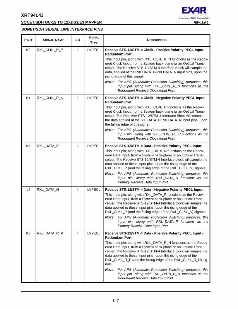
K2 RXL_CLKL_R_P I LVPECL Receive STS-12/STM-4 Clock - Positive Polarity PECL Input - Redundant Port:This input pin, along with RXL_CLKL_R_N functions as the Recov-ered Clock Input, from a System back-plane or an Optical Trans-ceiver. The Receive STS-12/STM-4 Interface Block will sample the data, applied at the RXLDATA_P/RXLDATA_N input pins, upon the rising edge of this signal.NOTE: For APS (Automatic Protection Switching) purposes, this
input pin, along with RXL_CLKL_R_N functions as the Redundant Receive Clock Input Port.
K1 RXL_CLKL_R_N I LVPECL Receive STS-12/STM-4 Clock - Negative Polarity PECL Input - Redundant Port:This input pin, along with RXL_CLKL_P functions as the Recov-ered Clock Input, from a System back-plane or an Optical Trans-ceiver. The Receiver STS-12/STM-4 Interface Block will sample the data applied at the RXLDATA_P/RXLDATA_N input pins, upon the falling edge of this signal.NOTE: For APS (Automatic Protection Switching) purposes, this
input pin, along with RXL_CLKL_R_ P functions as the Redundant Receive Clock Input Port.
K4 RXL_DATA_P I LVPECL Receive STS-12/STM-4 Data - Positive Polarity PECL Input:This input pin, along with RXL_DATA_N functions as the Recov-ered Data Input, from a System back-plane or an Optical Trans-ceiver. The Receive STS-12/STM-4 Interface block will sample the data applied to these input pins, upon the rising edge of the RXL_CLKL_P (and the falling edge of the RXL_CLKL_N) signals.NOTE: For APS (Automatic Protection Switching) purposes, this
input pin, along with RXL_DATA_N functions as the Primary Receive Data Input Port.
XRT94L43REV. 1.0.2 SONET/SDH OC-12 TO 12XDS3/E3 MAPPER
L4 RXL_DATA_N I LVPECL Receive STS-12/STM-4 Data - Negative Polarity PECL Input:This input pin, along with RXL_DATA_P functions as the Recov-ered Data Input, from a System back-plane or an Optical Trans-ceiver. The Receive STS-12/STM-4 Interface block will sample the data applied to these input pins, upon the rising edge of the RXL_CLKL_P (and the falling edge of the RXL_CLKL_N) signals.NOTE: For APS (Automatic Protection Switching) purposes, this
input pin, along with RXL_DATA_P functions as the Primary Receive Data Input Port.
K3 RXL_DATA_R_P I LVPECL Receive STS-12/STM-4 Data - Positive Polarity PECL Input - Redundant Port:This input pin, along with RXL_DATA_R_N functions as the Recov-ered Data Input, from a System back-plane or an Optical Trans-ceiver. The Receive STS-12/STM-4 Interface block will sample the data applied to these input pins, upon the rising edge of the RXL_CLKL_R_P (and the falling edge of the RXL_CLKL_R_N) sig-nals.NOTE: For APS (Automatic Protection Switching) purposes, this
input pin, along with RXL_DATA_R_N functions as the Redundant Receive Data Input Port.
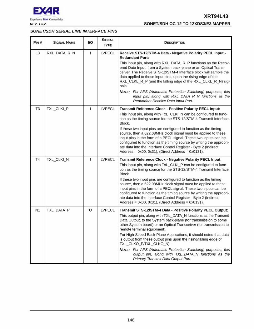
L3 RXL_DATA_R_N I LVPECL Receive STS-12/STM-4 Data - Negative Polarity PECL Input - Redundant Port:This input pin, along with RXL_DATA_R_P functions as the Recov-ered Data Input, from a System back-plane or an Optical Trans-ceiver. The Receive STS-12/STM-4 Interface block will sample the data applied to these input pins, upon the rising edge of the RXL_CLKL_R_P (and the falling edge of the RXL_CLKL_R_N) sig-nals.NOTE: For APS (Automatic Protection Switching) purposes, this
input pin, along with RXL_DATA_R_N functions as the Redundant Receive Data Input Port.
T3 TXL_CLKI_P I LVPECL Transmit Reference Clock - Positive Polarity PECL Input:This input pin, along with TxL_CLKI_N can be configured to func-tion as the timing source for the STS-12/STM-4 Transmit Interface Block.If these two input pins are configured to function as the timing source, then a 622.08MHz clock signal must be applied to these input pins in the form of a PECL signal. These two inputs can be configured to function as the timing source by writing the appropri-ate data into the Interface Control Register - Byte 2 (Indirect Address = 0x00, 0x31), (Direct Address = 0x0131).
SONET/SDH SERIAL LINE INTERFACE PINS
PIN # SIGNAL NAME I/OSIGNAL
TYPEDESCRIPTION
14
XRT94L43 SONET/SDH OC-12 TO 12XDS3/E3 MAPPER REV. 1.0.2
15
T4 TXL_CLKI_N I LVPECL Transmit Reference Clock - Negative Polarity PECL Input:This input pin, along with TxL_CLKI_P can be configured to func-tion as the timing source for the STS-12/STM-4 Transmit Interface Block.If these two input pins are configured to function as the timing source, then a 622.08MHz clock signal must be applied to these input pins in the form of a PECL signal. These two inputs can be configured to function as the timing source by writing the appropri-ate data into the Interface Control Register - Byte 2 (Indirect Address = 0x00, 0x31), (Direct Address = 0x0131).
N1 TXL_DATA_P O LVPECL Transmit STS-12/STM-4 Data - Positive Polarity PECL Output:This output pin, along with TXL_DATA_N functions as the Transmit Data Output, to the System back-plane (for transmission to some other System Board) or an Optical Transceiver (for transmission to remote terminal equipment).For High-Speed Back-Plane Applications, it should noted that data is output from these output pins upon the rising/falling edge of TXL_CLKO_P/TXL_CLKO_N).NOTE: For APS (Automatic Protection Switching) purposes, this
output pin, along with TXL_DATA_N functions as the Primary Transmit Data Output Port.
N2 TXL_DATA_N O LVPECL Transmit STS-12/STM-4 Data - Negative Polarity PECL Output:This output pin, along with TXL_DATA_P functions as the Transmit Data Output, to the System back-plane (for transmission to some other System Board) or an Optical Transceiver (for transmission to remote terminal equipment).For High-Speed Back-Plane Applications, it should noted that data is output from these output pins upon the rising/falling edge of TXL_CLKO_P/TXL_CLKO_N).NOTE: For APS (Automatic Protection Switching) purposes, this
output pin, along with TXL_DATA_P functions as the Primary Transmit Data Output Port.
P1 TXL_DATA_R_P O LVPECL Transmit STS-12/STM-4 Data - Positive Polarity PECL Output - Redundant Port:This output pin, along with TXL_DATA_R_N functions as the Transmit Data Output, to the System back-plane (for transmission to some other System Board) or an Optical Transceiver (for trans-mission to remote terminal equipment).For High-Speed Back-Plane Applications, it should noted that data is output from these output pins upon the rising/falling edge of TXL_CLKO_R_P/TXL_CLKO_R_N).NOTE: For APS (Automatic Protection Switching) purposes, this
output pin, along with TXL_DATA_N functions as the Redundant Transmit Data Output Port.
SONET/SDH SERIAL LINE INTERFACE PINS
PIN # SIGNAL NAME I/OSIGNAL
TYPEDESCRIPTION
XRT94L43REV. 1.0.2 SONET/SDH OC-12 TO 12XDS3/E3 MAPPER
16
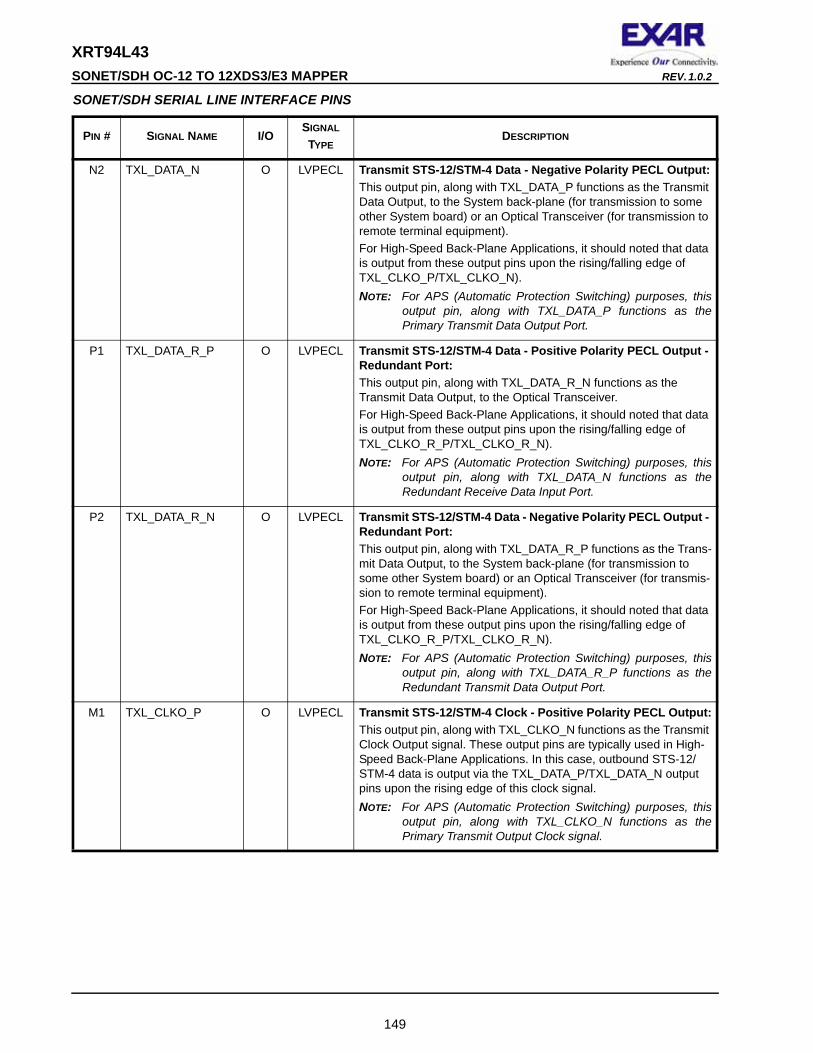
P2 TXL_DATA_R_N O LVPECL Transmit STS-12/STM-4 Data - Negative Polarity PECL Output - Redundant Port:This output pin, along with TXL_DATA_R_P functions as the Trans-mit Data Output, to the System back-plane (for transmission to some other System Board) or an Optical Transceiver (for transmis-sion to remote terminal equipment).For High-Speed Back-Plane Applications, it should noted that data is output from these output pins upon the rising/falling edge of TXL_CLKO_R_P/TXL_CLKO_R_N).NOTE: For APS (Automatic Protection Switching) purposes, this
output pin, along with TXL_DATA_R_P functions as the Redundant Transmit Data Output Port.
M1 TXL_CLKO_P O LVPECL Transmit STS-12/STM-4 Clock - Positive Polarity PECL Output:This output pin, along with TXL_CLKO_N functions as the Transmit Clock Output signal. These output pins are typically used in High-Speed Back-Plane Applications. In this case, outbound STS-12/STM-4 data is output via the TXL_DATA_P/TXL_DATA_N output pins upon the rising edge of this clock signal.NOTE: For APS (Automatic Protection Switching) purposes, this
output pin, along with TXL_CLKO_N functions as the Primary Transmit Output Clock signal.
M2 TXL_CLKO_N O LVPECL Transmit STS-12/STM-4 Clock - Negative Polarity PECL Out-put:This output pin, along with TXLCLKO_P functions as the Transmit Clock Output signal. These output pins are typically used in High-Speed Back-Plane Applications. In this case, outbound STS-12/STM-4 data is output via the TXL_DATA_P/TXL_DATA_N output pins upon the falling edge of this clock signal.NOTE: For APS (Automatic Protection Switching) purposes, this
output pin, along with TXL_CLKO_N functions as the Primary Transmit Output Clock signal.
R1 TXL_CLKO_R_P O LVPECL Transmit STS-12/STM-4 Clock - Positive Polarity PECL Output - Redundant Port:This output pin, along with TXL_CLKO_R_N functions as the Transmit Clock Output signal. These output pins are typically used in High-Speed Back-Plane Applications. In this case, outbound STS-12/STM-4 data is output via the TXL_DATA_R_P/TXL_DATA_R_N output pins upon the rising edge of this clock sig-nal.NOTE: For APS (Automatic Protection Switching) purposes, this
output pin, along with TXL_CLKO_R_N functions as the Redundant Transmit Output Clock signal.
SONET/SDH SERIAL LINE INTERFACE PINS
PIN # SIGNAL NAME I/OSIGNAL
TYPEDESCRIPTION
XRT94L43 SONET/SDH OC-12 TO 12XDS3/E3 MAPPER REV. 1.0.2
17
R2 TXL_CLKO_R_N O LVPECL Transmit STS-12/STM-4 Clock - Negative Polarity PECL Output - Redundant Port:This output pin, along with TXL_CLKO_R_P functions as the Transmit Clock Output signal. These output pins are typically used in High-Speed Back-Plane Applications. In this case, outbound STS-12/STM-4 data is output via the TXL_DATA_R_P/TXL_DATA_R_N output pins upon the rising edge of this clock sig-nal.For APS (Automatic Protection Switching) purposes, this output pin, along with TXL_CLKO_R_P functions as the Redundant Transmit Output Clock signal.
R4 REFCLK I TTL 77.76MHz or 622.08MHz Clock Synthesizer Reference Clock Input Pin:The function of this input pin depends upon whether or not the Transmit STS-12/STM-4 Clock Synthesizer block is enabled.If Clock Synthesizer is Enabled.If the Transmit STS-12/STSM-4 Clock Synthesizer block is to be used to generate the 77.76MHz and/or 622.08MHz clock signal for the STS-12/STM-4 block, then a clock signal of either of the follow-ing frequencies, must be applied to this input pin.
• 12.96MHz
• 19.44MHz
• 51.84 MHz
• 77.76 MHzAfterwards, the appropriate data needs to be written into the Inter-face Control Register - Byte 2 (Indirect Address = 0x00, 0x31), (Direct Address = 0x0131) in order to;(1) configure the Clock Synthesizer Block to accept any of the above-mentioned signals and generate a 77.76MHz or 622.08MHz clock signal,(2) to configure the Clock Synthesizer to function as the Clock Source for the STS-12/STM-4 block.If Clock Synthesizer is NOT Enabled:If the Transmit STS-12/STSM-4 Clock Synthesizer block is NOT to be used to generate the 77.76MHz and/or 622.08MHz clock signal for the STS-12/STM-4 block, then a 77.76MHz clock signal must be applied to this input pin.
AF6 LOS I TTL Loss of Optical Carrier Input - Primary:The Loss of Carrier output (from the Optical Transceiver) should be connected to this input pin.If this input pin is pulled "High", then the Primary Receive STS-12 TOH Processor block will declare a Loss of Optical Carrier condi-tion.NOTE: This input pin is only active if the Primary Port is active. This
input pin is inactive if the Redundant Port is active.
SONET/SDH SERIAL LINE INTERFACE PINS
PIN # SIGNAL NAME I/OSIGNAL
TYPEDESCRIPTION
XRT94L43REV. 1.0.2 SONET/SDH OC-12 TO 12XDS3/E3 MAPPER
AE6 LOS-R I TTL Loss of Optical Carrier Input - Redundant:The Loss of Carrier output (from the Optical Transceiver) should be connected to this input pin.If this input pin is pulled "High", then the Redundant Receive STS-12 TOH Processor block will declare a Loss of Optical Carrier con-dition.NOTE: This input pin is only active if the Redundant Port is active.
This input pin is inactive if the Primary Port is active.
AB7 EXSWITCH O CMOS External (APS) Switch Output Pin:This output pin can be used to permit the XRT94L43 to perform APS externally. Specifically, this output pin can be connected to some circuitry that permits the re-direction of STS-12/STM-4 traffic, should an APS event be needed.NOTE: This output pin is disabled if the EXSWITCHDIS input pin
number AB6 is pulled "High".
AB6 EXSWITCHDIS I TTL External (APS) Switch Disable:This input pin permits the user to configure the XRT94L43 to per-form Line APS Switching internally or externally.0 - Configures the XRT94L43 to perform APS externally. In this mode, the XRT94L43 will execute an APS by toggling the state of the "EXSWITCH" output pin.1 - Configures the XRT94L43 to perform APS internally. In this mode, each of the 12 Receive SONET POH Processor blocks (within the XRT94L43) will internally switch from processing the incoming STS-1 SPE data from the "Primary" Receive STS-12 TOH Processor block, to now processing the incoming STS-1 SPE data from the "Redundant" Receive STS-12 TOH Processor block (or vice-versa).
SONET/SDH SERIAL LINE INTERFACE PINS
PIN # SIGNAL NAME I/OSIGNAL
TYPEDESCRIPTION
18
XRT94L43 SONET/SDH OC-12 TO 12XDS3/E3 MAPPER REV. 1.0.2
19
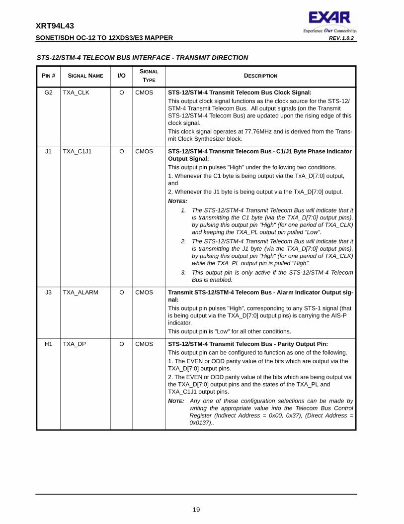
STS-12/STM-4 TELECOM BUS INTERFACE - TRANSMIT DIRECTION
PIN # SIGNAL NAME I/OSIGNAL
TYPEDESCRIPTION
G2 TXA_CLK O CMOS STS-12/STM-4 Transmit Telecom Bus Clock Signal:This output clock signal functions as the clock source for the STS-12/STM-4 Transmit Telecom Bus. All output signals (on the Transmit STS-12/STM-4 Telecom Bus) are updated upon the rising edge of this clock signal.This clock signal operates at 77.76MHz and is derived from the Trans-mit Clock Synthesizer block.
J1 TXA_C1J1 O CMOS STS-12/STM-4 Transmit Telecom Bus - C1/J1 Byte Phase Indicator Output Signal:This output pin pulses "High" under the following two conditions.1. Whenever the C1 byte is being output via the TxA_D[7:0] output, and 2. Whenever the J1 byte is being output via the TxA_D[7:0] output.NOTES:
1. The STS-12/STM-4 Transmit Telecom Bus will indicate that it is transmitting the C1 byte (via the TXA_D[7:0] output pins), by pulsing this output pin "High" (for one period of TXA_CLK) and keeping the TXA_PL output pin pulled "Low".
2. The STS-12/STM-4 Transmit Telecom Bus will indicate that it is transmitting the J1 byte (via the TXA_D[7:0] output pins), by pulsing this output pin "High" (for one period of TXA_CLK) while the TXA_PL output pin is pulled "High".
3. This output pin is only active if the STS-12/STM-4 Telecom Bus is enabled.
J3 TXA_ALARM O CMOS Transmit STS-12/STM-4 Telecom Bus - Alarm Indicator Output sig-nal:This output pin pulses "High", corresponding to any STS-1 signal (that is being output via the TXA_D[7:0] output pins) is carrying the AIS-P indicator.This output pin is "Low" for all other conditions.
H1 TXA_DP O CMOS STS-12/STM-4 Transmit Telecom Bus - Parity Output Pin:This output pin can be configured to function as one of the following.1. The EVEN or ODD parity value of the bits which are output via the TXA_D[7:0] output pins.2. The EVEN or ODD parity value of the bits which are being output via the TXA_D[7:0] output pins and the states of the TXA_PL and TXA_C1J1 output pins.NOTE: Any one of these configuration selections can be made by
writing the appropriate value into the Telecom Bus Control Register (Indirect Address = 0x00, 0x37), (Direct Address = 0x0137)..
XRT94L43REV. 1.0.2 SONET/SDH OC-12 TO 12XDS3/E3 MAPPER
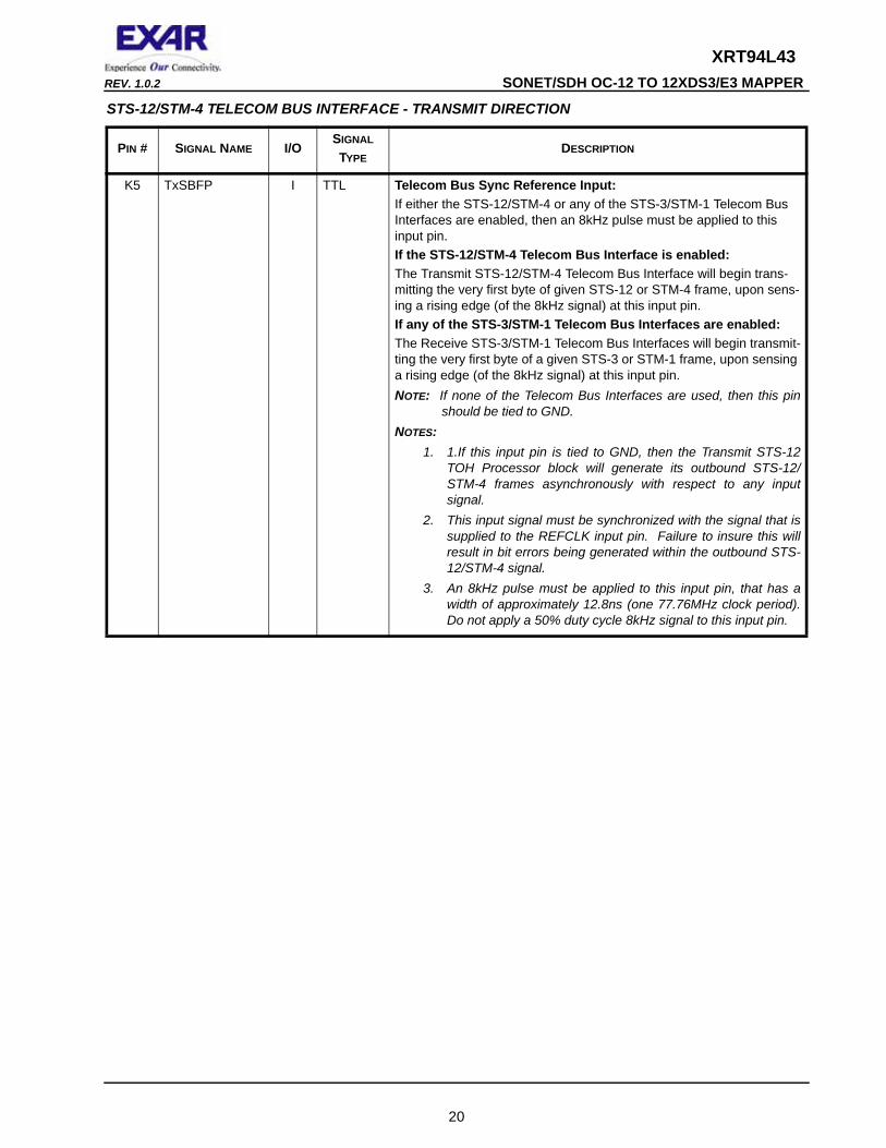
K5 TxSBFP I TTL Telecom Bus Sync Reference Input:If either the STS-12/STM-4 or any of the STS-3/STM-1 Telecom Bus Interfaces are enabled, then an 8kHz pulse must be applied to this input pin.If the STS-12/STM-4 Telecom Bus Interface is enabled:The Transmit STS-12/STM-4 Telecom Bus Interface will begin trans-mitting the very first byte of given STS-12 or STM-4 frame, upon sens-ing a rising edge (of the 8kHz signal) at this input pin.If any of the STS-3/STM-1 Telecom Bus Interfaces are enabled:The Receive STS-3/STM-1 Telecom Bus Interfaces will begin transmit-ting the very first byte of a given STS-3 or STM-1 frame, upon sensing a rising edge (of the 8kHz signal) at this input pin.NOTE: If none of the Telecom Bus Interfaces are used, then this pin
should be tied to GND.NOTES:
1. 1.If this input pin is tied to GND, then the Transmit STS-12 TOH Processor block will generate its outbound STS-12/STM-4 frames asynchronously with respect to any input signal.
2. This input signal must be synchronized with the signal that is supplied to the REFCLK input pin. Failure to insure this will result in bit errors being generated within the outbound STS-12/STM-4 signal.
3. An 8kHz pulse must be applied to this input pin, that has a width of approximately 12.8ns (one 77.76MHz clock period). Do not apply a 50% duty cycle 8kHz signal to this input pin.
STS-12/STM-4 TELECOM BUS INTERFACE - TRANSMIT DIRECTION
PIN # SIGNAL NAME I/OSIGNAL
TYPEDESCRIPTION
20
XRT94L43 SONET/SDH OC-12 TO 12XDS3/E3 MAPPER REV. 1.0.2
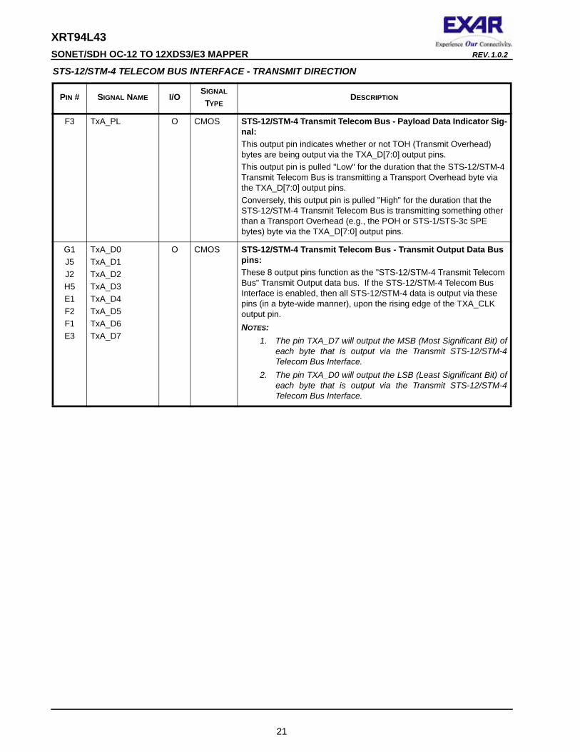
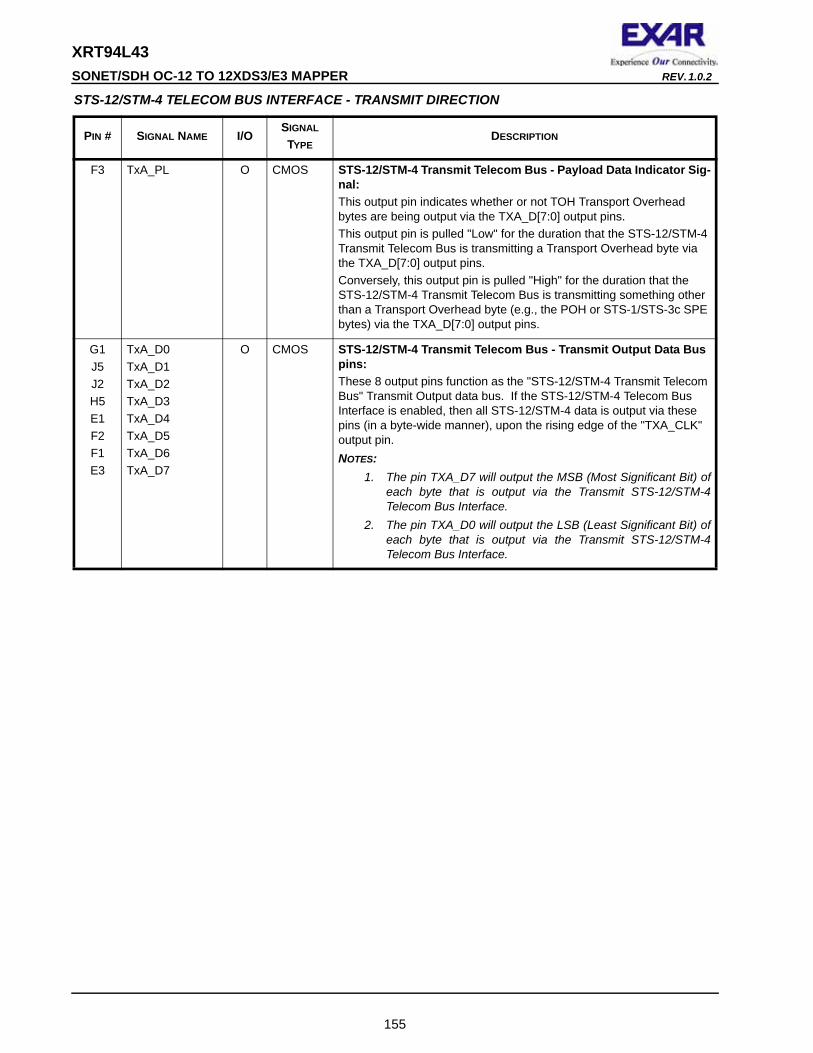
F3 TxA_PL O CMOS STS-12/STM-4 Transmit Telecom Bus - Payload Data Indicator Sig-nal:This output pin indicates whether or not TOH (Transmit Overhead) bytes are being output via the TXA_D[7:0] output pins.This output pin is pulled "Low" for the duration that the STS-12/STM-4 Transmit Telecom Bus is transmitting a Transport Overhead byte via the TXA_D[7:0] output pins.Conversely, this output pin is pulled "High" for the duration that the STS-12/STM-4 Transmit Telecom Bus is transmitting something other than a Transport Overhead (e.g., the POH or STS-1/STS-3c SPE bytes) byte via the TXA_D[7:0] output pins.
G1J5J2H5E1F2F1E3
TxA_D0TxA_D1TxA_D2TxA_D3TxA_D4TxA_D5TxA_D6TxA_D7
O CMOS STS-12/STM-4 Transmit Telecom Bus - Transmit Output Data Bus pins:These 8 output pins function as the "STS-12/STM-4 Transmit Telecom Bus" Transmit Output data bus. If the STS-12/STM-4 Telecom Bus Interface is enabled, then all STS-12/STM-4 data is output via these pins (in a byte-wide manner), upon the rising edge of the TXA_CLK output pin.NOTES:
1. The pin TXA_D7 will output the MSB (Most Significant Bit) of each byte that is output via the Transmit STS-12/STM-4 Telecom Bus Interface.
2. The pin TXA_D0 will output the LSB (Least Significant Bit) of each byte that is output via the Transmit STS-12/STM-4 Telecom Bus Interface.
STS-12/STM-4 TELECOM BUS INTERFACE - TRANSMIT DIRECTION
PIN # SIGNAL NAME I/OSIGNAL
TYPEDESCRIPTION
21
XRT94L43REV. 1.0.2 SONET/SDH OC-12 TO 12XDS3/E3 MAPPER
22
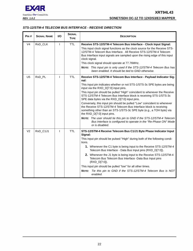
STS-12/STM-4 TELECOM BUS INTERFACE - RECEIVE DIRECTION
PIN # SIGNAL NAME I/OSIGNAL
TYPEDESCRIPTION
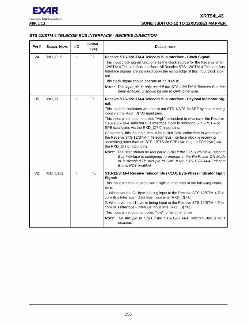
V4 RxD_CLK I TTL Receive STS-12/STM-4 Telecom Bus Interface - Clock Input Signal:This input clock signal functions as the clock source for the Receive STS-12/STM-4 Telecom Bus Interface. All Receive STS-12/STM-4 Telecom Bus Interface input signals are sampled upon the rising edge of this input clock signal.This clock signal should operate at 77.76MHz.NOTE: This input pin is only used if the STS-12/STM-4 Telecom Bus has
been enabled. It should be tied to GND otherwise.
U5 RxD_PL I TTL Receive STS-12/STM-4 Telecom Bus Interface - Payload Indicator Sig-nal:This input pin indicates whether or not STS-1/STS-3c SPE bytes are being input via the RXD_D[7:0] input pins.This input pin should be pulled "High" coincident to whenever the Receive STS-12/STM-4 Telecom Bus Interface block is receiving STS-1/STS-3c SPE data bytes via the RXD_D[7:0] input pins.Conversely, this input pin should be pulled "Low" coincident to whenever the Receive STS-12/STM-4 Telecom Bus Interface block is receiving something other than an STS-1/STS-3c SPE byte (e.g., a TOH byte) via the RXD_D[7:0] input pins. NOTE: The user should tie this pin to GND if the STS-12/STM-4 Telecom
Bus Interface is configured to operate in the "Re-Phase ON" Mode or is disabled.
V2 RxD_C1J1 I TTL STS-12/STM-4 Receive Telecom Bus C1/J1 Byte Phase Indicator Input Signal:This input pin should be pulsed "High" during both of the following condi-tions.
1. Whenever the C1 byte is being input to the Receive STS-12/STM-4 Telecom Bus Interface - Data Bus Input pins (RXD_D[7:0]).
2. Whenever the J1 byte is being input to the Receive STS-12/STM-4 Telecom Bus Telecom Bus Interface -Data Bus Input pins (RXD_D[7:0]).
This input pin should be pulled "low" for all other times.NOTE: Tie this pin to GND if the STS-12/STM-4 Telecom Bus is NOT
enabled.
XRT94L43 SONET/SDH OC-12 TO 12XDS3/E3 MAPPER REV. 1.0.2
U4 RxD_DP I TTL STS-12/STM-4 Receive Telecom Bus - Parity Input Pin:This input pin can be configured to function as one of the following.
1. The EVEN or ODD parity value of the bits which are input via the RXD_D[7:0] input pins.
2. The EVEN or ODD parity value of the bits which are being input via the RXD_D[7:0] input and the states of the RXD_PL and RXD_C1J1 input pins.
The Receive STS-12/STM-4 Telecom Bus Interface will use this pin to compute and verify the parity within the incoming STS-12/STM-4 data-stream. NOTES:
1. Any one of these configuration selections can be made by writing the appropriate value into the Telecom Bus Control register (Indirect Address = 0x00, 0x37, direct Address = 0x0137.
2. Tie this pin to GND if the STS-12/STM-4 Telecom Bus Interface is configured to operate in the Re-Phase ON Mode or is disabled.
T2 RxD_ALARM I TTL Receive STS-12/STM-4 Telecom Bus - Alarm Indicator Input:This input pin pulses "High" corresponding to any STS-1 signal that is car-rying the AIS-P indicator.More specifically, this input pin will be pulsed "High" coincident to when-ever a byte, corresponding to given STS-1 signal (that is carrying the AIS-P indicator) is being placed on the Receive STS-12/STM-4 Telecom Bus - Data Bus Input pins (RxD_D[7:0]). This input pin should be pulled "Low" at all other times.NOTES:
1. If the RxD_ALARM input signal pulses "High" for any given STS-1 signal (within the incoming STS-12), then the XRT94L43 will automatically declare the AIS-P defect for that particular STS-1 channel.
2. Tie this pin to GND if the STS-12/STM-4 Telecom Bus Interface has been cofigured to operate in the Re-Phase On Mode or is disbled.
U3V3U2T1V5U1W1V1
RxD_D0RxD_D1RxD_D2RxD_D3RxD_D4RxD_D5RxD_D6RxD_D7
I TTL Receive STS-12/STM-4 Receive Telecom Bus - Receive Input Data Bus pins:These 8 input pins function as the "Receive STS-12/STM4 Receive Tele-com Bus" Receive Input data bus. All incoming STS-12/STM-4 data is sampled and latched (into the XRT94L43 via these input pins) upon the rising edge of the RXD_CLK" input pin.NOTES:
1. 1.The user must insure that the MSB (Most Significant bit) of each incoming byte is input to the RXD_D7 input pin.
2. The user must also insure that the LSB (Least Significant bit) of each incoming byte is input to the RXD_D0 input pin.
3. The user should tie these pins to GND if the STS-12/STM-4 Telecom Bus is not enabled.
STS-12/STM-4 TELECOM BUS INTERFACE - RECEIVE DIRECTION
PIN # SIGNAL NAME I/OSIGNAL
TYPEDESCRIPTION
23
XRT94L43REV. 1.0.2 SONET/SDH OC-12 TO 12XDS3/E3 MAPPER
24
SONET/SDH OVERHEAD INTERFACE - TRANSMIT DIRECTION
PIN # SIGNAL NAME I/OSIGNAL
TYPEDESCRIPTION
H2 TxTOHClk O CMOS Transmit TOH Input Port - Clock Output:This output pin, along with the TxTOHEnable, TxTOHFrame output pins and the TxTOH and TxTOHIns input pins function as the Transmit TOH Input Port.The Transmit TOH Input Port allows the user to insert their own value for the TOH bytes (in the outbound STS-12/STM-4 signal).This output pin provides a clock signal. If the TxTOHEnable output pin is "High" and if the TxTOHIns input pin is pulled "High", then the user is expected to provide a given bit (within the TOH) to the TxTOH input pin, upon the falling edge of this clock signal. The data, residing on the TxTOH input pin will be latched into the XRT94L43 upon the rising edge of this clock signal.NOTE: The Transmit TOH Input Port only support the insertion of the
TOH within the first STS-1, within the outbound STS-12 signal.
H4 TxTOHEnable O CMOS Transmit TOH Input Port - TOH Enable (or READY) indicator:This output pin, along with the TxTOHClk, TxTOHFrame output pins and the TxTOH and TxTOHIns input pins function as the Transmit TOH Input Port.This output pin will toggle and remain "High" anytime the Transmit TOH Input Port is ready to externally accept TOH data.If it is desired to externally insert a value of TOH into the outbound STS-12 data stream via the Transmit TOH Input Port, then do the following:
• Continuously sample the state of TxTOHFrame and this output pin upon the rising edge of TxTOHClk.
• Whenever this output pin pulses "High", then the user's external circuitry should drive the TxTOHIns input pin "High".
• Next, the user should output the next TOH bit, onto the TxTOH input pin, upon the falling edge of TxTOHClk.
D1 TxTOH I TTL Transmit TOH Input Port - Input Pin:This input pin, along with the TxTOHIns input pin, the TxTOHEnable and TxTOHFrame and TxTOHClk output pins function as the Transmit TOH Input Port.If it is desired to externally insert a value of TOH into the outbound STS-12 data stream via the Transmit TOH Input Port, then do the following:
• Continuously sample the state of TxTOHFrame and TxTOHEnable upon the rising edge of TxTOHClk.
• Whenever TxTOHEnable pulses "High", then the user's external circuitry should drive the TxTOHIns input pin "High".
• Next, the user should output the next TOH bit, onto this input pin, upon the falling edge of TxTOHClk. The Transmit TOH Input Port will sample the data (on this input pin) upon the rising edge of TxTOHClk.
NOTE: Data at this input pin will be ignored (e.g., not sampled) unless the TxTOHEnable output pin is "High" and the TxTOHIns input pin is pulled "High".
XRT94L43 SONET/SDH OC-12 TO 12XDS3/E3 MAPPER REV. 1.0.2
25
G4 TxTOHFrame O CMOS Transmit TOH Input Port - STS-12/STM-4 Frame Indicator:This output pin, along with TxTOHClk, TxTOHEnable output pins, and the TxTOH and TxTOHIns input pins function as the Transmit TOH Input Port.This output pin will pulse "High" (for one period of TxTOHClk), one TxTOHClk clock period prior to the first TOH bit of a given STS-12 frame, being expected via the TxTOH input pin.If it is desired to externally insert a value of TOH into the outbound STS-12 data stream via the Transmit TOH Input Port, then do the following:
• Continuously sample the state of TxTOHEnable and this output pin upon the rising edge of TxTOHClk.
• Whenever the TxTOHEnable output pin pulse "High", then the user's external circuitry should drive the TxTOHIns input pin "High".
• Next, the user should output the next TOH bit, onto the TxTOH input pin, upon the falling edge of TxTOHClk.
NOTE: The external circuitry (which is being interfaced to the Transmit TOH Input Port can use this output pin to denote the boundary of STS-12 frames.
C1 TxTOHIns I TTL Transmit TOH Input Port - Insert Enable Input Pin:This input pin, along with the TxTOH input pin, and the TxTOHEnable, TxTOHFrame and TxTOHClk output pins function as the Transmit TOH Input Port.This input pin is used to either enable or disable the Transmit TOH Input Port.If this input pin is "Low", then the Transmit TOH Input Port will be dis-abled and will not sample and insert (into the outbound STS-12 data stream) any data residing on the TxTOH input, upon the rising edge of TxTOHClk.If this input pin is "High", then the Transmit TOH Input Port will be enabled. In this mode, whenever the TxTOHEnable output pin is also "High", the Transmit TOH Input Port will sample and latch any data that is presented on the TxTOH input pin, upon the rising edge of TxTOHClk.If it is desired to externally insert a value of TOH into the outbound STS-12 data stream via the Transmit TOH Input Port, then do the following:
• Continuously sample the state of TxTOHFrame and TxTOHEnable upon the rising edge of TxTOHClk.
• Whenever the TxTOHEnable output pin is sampled "High" then the user's external circuitry should drive this input pin "High".
• Next, the user should output the next TOH bit, onto the TxTOH input pin, upon the falling edge of TxTOHClk. The Transmit TOH Input Port will sample the data (on this input pin) upon the rising edge of TxTOHClk.
NOTE: Data applied to the TxTOH input pin will be ignored (e.g., not sampled) unless then the TxTOHEnable and this input pin are each "High".
SONET/SDH OVERHEAD INTERFACE - TRANSMIT DIRECTION
PIN # SIGNAL NAME I/OSIGNAL
TYPEDESCRIPTION
XRT94L43REV. 1.0.2 SONET/SDH OC-12 TO 12XDS3/E3 MAPPER
26
G3 TxLDCCEnable O CMOS Transmit - Line DCC Input Port - Enable Output Pin:This output pin, along with the TxTOHClk output pin and the TxLDCC input pin are used to insert the value for the D4, D5, D6, D7, D8, D9, D10, D11 and D12 bytes into the Transmit STS-12 TOH Processor Block. The Transmit STS-12 TOH Processor block will accept this data and will insert into the D4, D5, D6, D7, D8, D9, D10, D11 and D12 byte-fields, within the outbound STS-12 data-stream.The Line DCC HDLC Controller circuitry (which is connected to the TxTOHClk, the TxLDCC and this output pin, is suppose to do the follow-ing.1. It should continuously monitor the state of this output pin.2. Whenever this output pin pulses "High", then the Line DCC HDLC Controller circuitry should place the next Line DCC bit (to be inserted into the Transmit STS-12 TOH Processor block) onto the TxLDCC input pin, upon the falling edge of TxTOHClk.3. Any data that is placed on the TxLDCC input pin, will be sampled upon the rising edge of TxOHClk.
J4 TxSDCCEnable O CMOS Transmit - Section DCC Input Port - Enable Output Pin:This output pin, along with the TxTOHClk output pin and the TxSDCC input pin are used to insert the value for the D1, D2 and D3 bytes, into the Transmit STS-12 TOH Processor Block. The Transmit STS-12 TOH Processor block will accept this data and will insert into the D1, D2 and D3 byte-fields, within the outbound STS-12 data-stream.The Section DCC HDLC Controller circuitry (which is connected to the TxTOHClk, the TxSDCC and this output pin, is suppose to do the follow-ing.1. It should continuously monitor the state of this output pin.2. Whenever this output pin pulses "High", then the Section DCC HDLC Controller circuitry should place the next Section DCC bit (to be inserted into the Transmit STS-12 TOH Processor block) onto the TxSDCC input pin, upon the falling edge of TxTOHClk.3. Any data that is placed on the TxSDCC input pin, will be sampled upon the rising edge of TxOHClk.
E2 TxSDCC I TTL Transmit - Section DCC Input Port - Input Pin:This input pin, along with the TxSDCCEnable and the TxTOHClk output pins are used to insert a value for the D1, D2 and D3 bytes, into the Transmit STS-12 TOH Processor Block. The Transmit STS-12 TOH Processor block will accept this data and insert it into the D1, D2 and D3 byte fields, within the outbound STS-12 data-stream.The Section DCC HDLC Circuitry that is interfaced to this input pin, the TxSDCCEnable and the TxTOHClk pins is suppose to do the following.1. It should continuously monitor the state of the TxSDCCEnable input pin.2. Whenever the TxSDCCEnable input pin pulses "High", then the Sec-tion DCC HDLC Controller circuitry should place the next Section DCC bit (to be inserted into the Transmit STS-12 TOH Processor block) onto this input pin upon the falling edge of TxTOHClk.3. Any data that is placed on the TxSDCC input pin, will be sampled upon the rising edge of TxTOHClk.NOTE: Tie this pin to GND if it is not going to be used.
SONET/SDH OVERHEAD INTERFACE - TRANSMIT DIRECTION
PIN # SIGNAL NAME I/OSIGNAL
TYPEDESCRIPTION
XRT94L43 SONET/SDH OC-12 TO 12XDS3/E3 MAPPER REV. 1.0.2
27
H3 TxLDCC I TTL Transmit - Line DCC Input Port:This input pin, along with the TxLDCCEnable and the TxTOHClk pins are used to insert a value for the D4, D5, D6, D7, D8, D9, D10, D11 and D12 bytes, into the Transmit STS-12 TOH Processor Block. The Trans-mit STS-12 TOH Processor block will accept this data and insert it into the D4, D5, D6, D7, D8, D9, D10, D11 and D12 byte-fields, within the outbound STS-12 data-stream.Whatever Line DCC HDLC Controller Circuitry is interface to the this input pin, the TxLDCCEnable and the TxTOHClk is suppose to do the following.1. It should continuously monitor the state of the TxLDCCEnable input pin.2. Whenever the TxLDCCEnable input pin pulses "High", then the Sec-tion DCC Interface circuitry should place the next Line DCC bit (to be inserted into the Transmit STS-12 TOH Processor block) onto the TxLDCC input pin, upon the falling edge of TxTOHClk.3. Any data that is placed on the TxLDCC input pin, will be sampled upon the rising edge of TxTOHClk.NOTE: Tie this pin to GND, if it is not going to be used.
F4 TxE1F1E2Enable O CMOS Transmit E1-F1-E2 Byte Input Port - Enable (or Ready) Indicator Output Pin:This output pin, along with the TxTOHClk output pin and the TxE1F1E2 input pin are used to insert a value for the E1, F1 and E2 bytes, into the Transmit STS-12 TOH Processor Block. The Transmit STS-12 TOH Processor block will accept this data and will insert into the E1, F1 and E2 byte-fields, within the outbound STS-12 data-stream.Whatever external circuitry (which is connected to the TxTOHClk, the TxE1F1E2 and this output pin, is suppose to do the following.1. It should continuously monitor the state of this output pin.2. Whenever this output pin pulses "High", then the external circuitry should place the next orderwire bit (to be inserted into the Transmit STS-12 TOH Processor block) onto the TxE1F1E2 input pin, upon the falling edge of TxTOHClk.Any data that is placed on the TxE1F1E2 input pin, will be sampled upon the rising edge of TxOHClk.
D2 TxE1F2E2Frame O CMOS Transmit E1-F1-E2 Byte Input Port - Framing Output Pin:This output pin pulses "High" for one period of TxTOHClk, one TxTO-HClk bit-period prior to the Transmit E1-F1-E2 Byte Input Port expecting the very first byte of the E1 byte, within a given outbound STS-12 frame.
SONET/SDH OVERHEAD INTERFACE - TRANSMIT DIRECTION
PIN # SIGNAL NAME I/OSIGNAL
TYPEDESCRIPTION
XRT94L43REV. 1.0.2 SONET/SDH OC-12 TO 12XDS3/E3 MAPPER
28
J6 TxE1F1E2 I TTL Transmit E1-F1-E2 Byte Input Port - Input Pin:This input pin, along with the TxE1F1E2Enable and the TxTOHClk out-put pins are used to insert a value for the E1, F1 and E2 bytes, into the Transmit STS-12 TOH Processor Block. The Transmit STS-12 TOH Processor block will accept this data and insert it into the E1, F1 and E2 byte fields, within the outbound STS-12 data-stream.Whatever external circuitry that is interfaced to this input pin, the TxE1F1E2Enable and the TxTOHClk pins is suppose to do the follow-ing.1. It should continuously monitor the state of the TxE1F1E2Enable input pin.2. Whenever the TxE1F1E2Enable input pin pulses "High", then the external circuitry should place the next orderwire bit (to be inserted into the Transmit STS-12 TOH Processor block) onto this input pin upon the falling edge of TxTOHClk.3. Any data that is placed on the TxE1F1E2 input pin, will be sampled upon the rising edge of TxTOHClk.NOTE: Tie this pin to GND if it is not going to be used.
SONET/SDH OVERHEAD INTERFACE - TRANSMIT DIRECTION
PIN # SIGNAL NAME I/OSIGNAL
TYPEDESCRIPTION
XRT94L43 SONET/SDH OC-12 TO 12XDS3/E3 MAPPER REV. 1.0.2
I TTL Transmit Path Overhead Input Port - Input Pin.These input pins allow the following actions.1. Insertion oft the POH data into each of the 12 Transmit SONET POH Processor blocks (for insertion and transmission via the outbound STS-12 signal.2. Insertion of the POH data into each of the 12 Transmit STS-1 POH Processor blocks (for insertion and transmission via each of the out-bound STS-1 signals).3. Insertion of the TOH data into each of the 12 Transmit STS-1 TOH Processor blocks (for insertion and transmission via each of the out-bound STS-1 signals).The function of these input pins, depends upon whether or not the TOH data is inserted into the 12 Transmit STS-1 TOH Processor blocks.If the user is only inserting POH data via these input pins:In this mode, the external circuitry (which is being interfaced to the Transmit Path Overhead Input Port is suppose to monitor the following output pins.
• TxPOHFrame_n
• TxPOHEnable_n
• TxPOHClk_nThe TxPOHFrame_n output pin will toggle "High" upon the falling edge of TxPOHClk_n approximately one TxPOHClk_n period prior to the TxPOH port being ready to accept and process the first bit within the J1 byte (e.g., the first POH byte). The TxPOHFrame_n output pin will remain "High" for eight consecutive TxPOHClk_n periods. The external circuitry should use this pin to note STS-1 SPE frame boundaries.The TxPOHEnable_n output pin will toggle "High" upon the falling edge of TxPOHClk_n approximately one TxPOHClk_n period prior to the TxPOH port being ready to accept and process the first bit within a given POH byte.To externally insert a given POH byte, (1) assert the TxPOHIns_n input pin by toggling it "High" and (2) place the value of the first bit (within this particular POH byte) on this input pin upon the very next falling edge of TxPOHClk_n. This data bit will be sampled upon the very next rising edge of TxPOHClk_n. The external circuitry should continue to keep the TxPOHIns_n input pin "High" and advancing the next bits (within the POH bytes) upon each falling edge of TxPOHClk_n.If the user is inserting both POH and TOH data via these input pins:In this mode, the external circuitry (which is being interfaced to the Transmit Path Overhead Input Port is suppose to monitor the following output pins.
• TxPOHFrame_n
• TxPOHEnable_n
• TxPOHClk_n(continued below)
SONET/SDH OVERHEAD INTERFACE - TRANSMIT DIRECTION
PIN # SIGNAL NAME I/OSIGNAL
TYPEDESCRIPTION
XRT94L43REV. 1.0.2 SONET/SDH OC-12 TO 12XDS3/E3 MAPPER
I TTL If the user is inserting both POH and TOH data via these input pins:(Continued)The TxPOHFrame_n output pin will toggle "High" twice during a given STS-1 frame period. First, this output pin will toggle "High" coincident with the TxPOH port being ready to accept and process the A1 byte (e.g., the very first TOH byte). Second, this output pin will toggle "High" coincident with the TxPOH port being ready to accept and process the J1 byte (e.g., the very first POH byte).If the externally circuitry samples the TxPOHFrame_n output pin "High", and the TxPOHEnable_n output pin "Low", then the TxPOH port is now ready to accept and process the very first TOH byte.If the externally circuitry samples the TxPOHFrame_n output pin "High" and the TxPOHEnable_n output pin "High", then the TxPOH port is now ready to accept and process the very first POH byte.To externally insert a given POH or TOH byte, do the following;(1) Assert the TxPOHIns_n input pin by toggling it "High" and,(2) place the value of the first bit (within this particular POH or TOH byte) on this input upon the very next falling edge of TxPOHClk_n.This data bit will be sampled upon the very next rising edge of TxPOHClk_n. The external circuitry should continue to keep the TxPOHIns_n input pin "High" and advancing the next bits (within the POH bytes) upon each falling edge of TxPOHClk_n.NOTES:
1. If POH data is externally inserted into each of the 12 Transmit SONET POH Processor blocks, then these input pins cannot be used to externally insert POH data into each of the 12 Transmit STS-1 POH Processor blocks.
2. TOH data can be externally inserted into each of the 12 Transmit STS-1 TOH Processor blocks, only if POH data is NOT externally inserted into each of the 12 Transmit SONET POH Processor blocks.
O CMOS Transmit Path Overhead Input Port - Clock Output pin:These output pins, along with TxPOH_n, TxPOHEnable_n, TxPOHIns_n and TxPOHFrame_n function as the Transmit Path Over-head (TxPOH) Input Port.The TxPOHFrame_n and TxPOHEnable_n output pins are updated upon the falling edge this clock output signal. The TxPOHIns_n input pins and the data residing on the TxPOH_n input pins are sampled on the rising edge of this clock signal.
SONET/SDH OVERHEAD INTERFACE - TRANSMIT DIRECTION
PIN # SIGNAL NAME I/OSIGNAL
TYPEDESCRIPTION
XRT94L43 SONET/SDH OC-12 TO 12XDS3/E3 MAPPER REV. 1.0.2
O CMOS Transmit Path Overhead Input Port - Frame Output pin:These output pins, along with the TxPOH_n, TxPOHEnable_n, TxPOHIns_n and TxPOHClk_n function as the Transmit Path Overhead Input Port.The function of these output pins depends upon whether POH or TOH data is inserted via the TxPOH_n input pins.If the user is only inserting POH data via these input pins:In this mode, the TxPOH port will pulse these output pins "High" when-ever it is ready to accept and process the J1 byte (e.g., the very first POH byte) via this port.If the user is inserting both POH and TOH data via these input pins:In this mode, the TxPOH port will pulse these output pins "High" coinci-dent with the following.1. Whenever the TxPOH port is ready to accept and process the A1 byte (e.g., the very first TOH byte) via this port.2. Whenever the TxPOH port is ready to accept and process the J1 byte (e.g., the very first POH byte) via this port.NOTE: The external circuitry can determine whether the TxPOH port is
expecting the A1 byte or the J1 byte, by checking the state of the corresponding TxPOHEnable output pin. If the TxPOHEnable_n output pin is "Low" while the TxPOHFrame_n output pin is "High", then the TxPOH port is ready to process the A1 (TOH) bytes.
If the TxPOHEnable_n output pin is "High" while the TxPOHFrame_n output pin is "High", then the TxPOH port is ready to process the J1 (POH) bytes.
SONET/SDH OVERHEAD INTERFACE - TRANSMIT DIRECTION
PIN # SIGNAL NAME I/OSIGNAL
TYPEDESCRIPTION
XRT94L43REV. 1.0.2 SONET/SDH OC-12 TO 12XDS3/E3 MAPPER
I TTL Transmit Path Overhead Input Port - Insert Enable Input pin:These input pins, along with TxPOH_n, TxPOHEnable_n, TxPOHFrame_n and TxPOHClk_n function as the Transmit Path Over-head (TxPOH) Input Port.These input pins are used to enable or disable the TxPOH input port.If these input pins are pulled "High", then the TxPOH port will sample and latch data via the corresponding TxPOH input pins, upon the rising edge of TxPOHClk_n.Conversely, if these input pins are pulled "Low", then the TxPOH port will NOT sample and latch data via the corresponding TxPOH input pins.NOTE: If the TxPOHIns_n input pin is pulled "Low", this setting will be
overridden if, the Transmit SONET/STS-1 POH Processor or Transmit STS-1 TOH Processor blocks are configured to accept certain POH or TOH overhead bytes via the external port.
O CMOS Transmit Path Overhead Input Port - POH Indicator Output pin:These output pins, along with TxPOH_n, TxPOHIns_n, TxPOHFrame_n and TxPOHClk_n function as the Transmit Path Overhead (TxPOH) Input Port.These output pins will pulse "High" anytime the TxPOH port is ready to accept and process POH bytes. These output pins will be "Low" at all other times.
SONET/SDH OVERHEAD INTERFACE - TRANSMIT DIRECTION
PIN # SIGNAL NAME I/OSIGNAL
TYPEDESCRIPTION
32
XRT94L43 SONET/SDH OC-12 TO 12XDS3/E3 MAPPER REV. 1.0.2
33
STS-3/STM-1 TELECOM BUS INTERFACE - TRANSMIT DIRECTION
PIN # SIGNAL NAME I/OSIGNAL
TYPEDESCRIPTION
E15 STS3TxA_CLK_0
TxSBCLK_0
DMO_0
I TTL STS-3 Transmit Telecom Bus Clock Input/STM-1 Sub-Rate Clock/DMO_0 (General Purpose) input Pin:The function of this input pin depends upon whether or not theSTS-3/STM-1 Telecom Bus Interface for Channel 0 has been enabled.If STS-3/STM-1 Telecom Bus (Channel 0) has been enabled - STS-3 Transmit Telecom Bus Transmit Clock Input - Channel 0:This input clock signal functions as the clock source for the STS-3/STM-1 Transmit Telecom Bus, associated with Channel 0. All input signals (e.g., STS3TxA_ALARM_0, STS3TxA_D_0[7:0], STS3TxA_DP_0, STS3TxA_PL_0, STS3TxA_C1J1_0) are sampled upon the falling edge of this input clock signal.This clock signal should operate at 19.44MHz.If STS-3/STM-1 Telecom Bus (Channel 0) is disabled - DMO_0 (General Purpose) Input Pin:This input pin can be used as a general purpose input pin.The state of this input pin can be determined by reading the state of Bit 2 (DMO) within the Line Interface Scan Register associated with Channel 0 (Address = 0x1E, 0x81), (Direct Address = 0x1F81).NOTE: For Product Legacy purposes, this pin is called DMO_0,
because one possible application is to tie this input pin to a DMO (Drive Monitor Output) output pin, from one of Exar's XRT73L0X/XRT75L0X DS3/E3/STS-1 LIU devices. However, this input pin, and the corresponding register bit can be used for any purpose.
C26 STS3TxA_CLK_1
TxSBCLK_1
DMO_1
I TTL STS-3 Transmit Telecom Bus Clock Input/STM-1 Sub-Rate Clock/DMO_1 (General Purpose) input Pin:See definition of Pin # E15 above replacing Channel 0 with Channel 1.If STS-3/STM-1 Telecom Bus (Channel 1) has been enabled - STS-3 Transmit Telecom Bus Clock Input - Channel 1:
If STS-3/STM-1 Telecom Bus (Channel 1) is disabled - DMO_1 (General Purpose) Input Pin:
AE25 STS3TxA_CLK_2
TxSBCLK_2
DMO_2
I TTL STS-3 Transmit Telecom Bus Clock Input/STM-1 Sub-Rate Clock/DMO_2 (General Purpose) input Pin:See definition of Pin # E15 above replacing Channel 0 with Channel 2.If STS-3/STM-1 Telecom Bus (Channel 2) has been enabled - STS-3 Transmit Telecom Bus Transmit Clock Input - Channel 2:
If STS-3/STM-1 Telecom Bus (Channel 2) is disabled - DMO_2 -Drive Monitor Output Input (from XRT73L0X LIU IC) - Channel 2:
XRT94L43REV. 1.0.2 SONET/SDH OC-12 TO 12XDS3/E3 MAPPER
34
AD17 STS3TxA_CLK_3
TxSBCLK_3
DMO_3
I TTL STS-3 Transmit Telecom Bus Clock Input/STM-1 Sub-Rate Clock/DMO_3 (General Purpose) input Pin:See definition of Pin # E15 above replacing Channel 0 with Channel 3.If STS-3/STM-1 Telecom Bus (Channel 3) has been enabled -STS-3 Transmit Telecom Bus Clock Input - Channel 3:
If STS-3/STM-1 Telecom Bus (Channel 3) is disabled - DMO_3 (General Purpose) Input Pin:
E14 STS3TxA_PL_0
TxSBFrame_0
RLOL_0
I TTL Transmit STS-3/STM-1 Telecom Bus Interface - Payload Indica-tor Signal - Channel 0/RLOL_0 (General Purpose) input Pin:The function of this input depends upon whether or not theSTS-3/STM-1 Telecom Bus Interface for Channel 0 has been enabled.If STS-3/STM-1 Telecom Bus (Channel 0) has been enabled - Transmit STS-3/STM-1 Telecom Bus Interface - Payload Indica-tor Signal - Channel 0:This input pin indicates whether or not Transport Overhead (TOH) bytes are being input via the TXA_D_0[7:0] input pins.This input pin should be pulled "Low" for the duration that the STS-3/STM-1 Transmit Telecom Bus is receiving a TOH byte, via the TXA_D_0[7:0] input pins.NOTE: This input signal is sampled upon the falling edge of
STS3TxA_CLK_0.If STS-3/STM-1 Telecom Bus (Channel 0) is disabled - RLOL_0 (General Purpose) Input Pin.This input pin can be used as a general purpose input pin.The state of this input pin can be determined by reading the state of Bit 1 (RLOL) within the Line Interface Scan Register associated with Channel 0 (Address = 0x1E, 0x81), (Direct Address = 0x1F81).NOTE: For Product Legacy purposes, this pin is called RLOL_0
because one possible application is to tie this input pin to a RLOL (Receive Loss of Lock) output pin, from one of Exar's XRT73L0X/XRT75L0X DS3/E3/STS-1 LIU devices. However, this input pin and the corresponding register bit can be used for any purpose.
A26 STS3TxA_PL_1
TxSBFrame_1
RLOL_1
I TTL Transmit STS-3/STM-1 Telecom Bus Interface - Payload Indica-tor Signal - Channel 1/RLOL_1 (General Purpose) input Pin:See definition of Pin # E14 above replacing Channel 0 with Channel 1.If STS-3/STM-1 Telecom Bus (Channel 1) has been enabled - Transmit STS-3/STM-1 Telecom Bus Interface - Payload Indica-tor Signal - Channel 1:
If STS-3/STM-1 Telecom Bus (Channel 1) is disabled - RLOL_1 (General Purpose) Input Pin:
STS-3/STM-1 TELECOM BUS INTERFACE - TRANSMIT DIRECTION
PIN # SIGNAL NAME I/OSIGNAL
TYPEDESCRIPTION
XRT94L43 SONET/SDH OC-12 TO 12XDS3/E3 MAPPER REV. 1.0.2
35
AD25 STS3TxA_PL_2
TxSBFrame_2
RLOL_2
I TTL Transmit STS-3/STM-1 Telecom Bus Interface - Payload Indica-tor Signal - Channel 2/RLOL_2 (General Purpose) input Pin:See definition of Pin # E15 above replacing Channel 0 with Channel 2.If STS-3/STM-1 Telecom Bus (Channel 2) has been enabled - Transmit STS-3/STM-1 Telecom Bus Interface - Payload Indica-tor Signal - Channel 2:
If STS-3/STM-1 Telecom Bus (Channel 2) is disabled - RLOL_2 (General Purpose) Input Pin:
AB17 STS3TxA_PL_3
TxSBFrame_3
RLOL_3
I TTL Transmit STS-3/STM-1 Telecom Bus Interface - Payload Indica-tor Signal - Channel 3/RLOL_3 (General Purpose) input Pin:See definition of Pin # E15 above replacing Channel 0 with Channel 3.If STS-3/STM-1 Telecom Bus (Channel 3) has been enabled - Transmit STS-3/STM-1 Telecom Bus Interface - Payload Indica-tor Signal - Channel 3:
If STS-3/STM-1 Telecom Bus (Channel 3) is disabled - RLOL_3 (General Purpose) Input Pin:
STS-3/STM-1 TELECOM BUS INTERFACE - TRANSMIT DIRECTION
PIN # SIGNAL NAME I/OSIGNAL
TYPEDESCRIPTION
XRT94L43REV. 1.0.2 SONET/SDH OC-12 TO 12XDS3/E3 MAPPER
Transmit STS-3/STM-1 Telecom Bus Interface C1/J1 Byte Phase Indicator Input Signal (Channel 0); DS3/E3 Framer Block LCV/RxNEG Input Pin - Channel 8:The function of this pin depends upon whether or not theSTS-3/STM-1 Telecom Bus Interface for Trlrcom Bus Channel 0 has been enabled.If STS-3/STM-1 Telecom Bus (Telecom Bus Channel 0) has been enabled - Transmit STS-3/STM-1 Telecom Bus Interface C1/J1 Byte Phase Indicator Input Signal (Channel 0):This input pin should be pulsed "high" during both of the following conditions.
1. Whenever the C1 byte is being input to the STS-3/STM-1 Transmit Telecom Bus (TXA_D_0[7:0]) input pins.
2. Whenever the J1 byte is being input to the STS-3/STM-1 Transmit Telecom Bus (TXA_D_0[7:0]) input pins.
If STS-3/STM-1 Telecom Bus (Channel 0) is disabled - DS3/E3 Framer Block LCV/NEG Input - Channel 8:If the STS-3/STM-1 Telecom Bus (Channel 0) is disabled and if the DS3/E3 Framer block (associated with Channel 8) is enabled then this pin will function as either an LCV or an RxNEG input pin.If Channel 8 is configured to operate in the Single- Rail Mode, and if the Primary Frame Synchronizer block is configured to operate in the Ingress Path - ING_LCV_IN_8 Input pin:If the Primary Frame Synchronizer Block (associated with Channel 8) is configured to operate in the Ingress Path, and if Channel 8 is con-figured to operate in the Single-Rail Mode, then this input pin will function as the "LCV" (Line Code Violation) input pin. In this case, the user should connect this particular input pin to the "LCV" output pin of the corresponding DS3/E3/STS-1 LIU Channel. If Channel 8 is configured to operate in the Dual-Rail Mode, and if the Primary Frame Synchronizer block is configured to oper-ate in the Ingress Path - ING_RxNEG_IN_8:If the Primary Frame Synchronizer block (associated with Channel 8) is configured to operate in the Ingress Path, and if Channel 8 is con-figured to operate in the Dual-Rail Mode, then this input pin will func-tion as the "RxNEG" (Negative Polarity Data) input pin. In this case, the user should connect this particular input to the "RxNEG" output pin of the corresponding DS3/E3/STS-1 LIU Channel.NOTE: This pin is inactive if the Primary Frame Synchronizer block
(associated with Channel 8) is NOT configured to operate in the Ingress Path.
STS-3/STM-1 TELECOM BUS INTERFACE - TRANSMIT DIRECTION
PIN # SIGNAL NAME I/OSIGNAL
TYPEDESCRIPTION
XRT94L43 SONET/SDH OC-12 TO 12XDS3/E3 MAPPER REV. 1.0.2
37
J23
STS3TxA_C1J1_1
ING_LCV_IN_9ING_RxNEG_IN_9
TxSBFrame_1
I/O TTL/CMOS
Transmit STS-3/STM-1 Telecom Bus Interface - C1/J1 Byte Phase Indicator Input Signal (Channel 1); DS3/E3 Framer Block LCV/RxNEG Input Pin - Channel 9:The function of this pin depends upon whether or not theSTS-3/STM-1 Telecom Bus Interface for Telecom Bus Channel 1 has been enabled.If STS-3/STM-1 Telecom Bus (Telecom Bus Channel 1) has been enabled - Transmit STS-3/STM-1 Telecom Bus Interface C1/J1 Byte Phase Indicator Input Signal (Channel 1):This input pin should be pulsed "High" during both of the following conditions.
1. Whenever the C1 byte is being input to the STS-3/STM-1 Transmit Telecom Bus (TXA_D_1[7:0]) input pins.
2. Whenever the J1 byte is being input to the STS-3/STM-1 Transmit Telecom Bus (TXA_D_1[7:0]) input pins.
If STS-3/STM-1 Telecom Bus (Channel 1) is disabled - DS3/E3 Framer Block LCV/RxNEG Input - Channel 9):If the STS-3/STM-1 Telecom Bus (Channel 1) is disabled and if the DS3/E3 Framer block is enabled then this pin will function as either an LCV or RxNEG input pin.If Channel 9 is configured to operate in the Single- Rail Mode, and if the Primary Frame Synchronizer block is configured to operate in the Ingress Path - ING_LCV_IN_9 Input pin:If the Primary Frame Synchronizer Block (associated with Channel 9) is configured to operate in the Ingress Path, and if Channel 8 is con-figured to operate in the Single-Rail Mode, then this input pin will function as the "LCV" (Line Code Violation) input pin. In this case, the user should connect this particular input pin to the "LCV" output pin of the corresponding DS3/E3/STS-1 LIU Channel.If Channel 9 is configured to operate in the Dual-Rail Mode, and if the Primary Frame Synchronizer block is configured to oper-ate in the Ingress Path - ING_RxNEG_IN_9:If the Primary Frame Synchronizer block (associated with Channel 9) is configured to operate in the Ingress Path, and if Channel 9 is con-figured to operate in the Dual-Rail Mode, then this input pin will func-tion as the "RxNEG" (Negative Polarity Data) input pin. In this case, the user should connect this particular input to the "RxNEG" output pin of the corresponding DS3/E3/STS-1 LIU Channel.NOTE: This pin is inactive if the Primary Frame Synchronizer block
(associated with Channel 9) is NOT configured to operate in the Ingress Path.
STS-3/STM-1 TELECOM BUS INTERFACE - TRANSMIT DIRECTION
PIN # SIGNAL NAME I/OSIGNAL
TYPEDESCRIPTION
XRT94L43REV. 1.0.2 SONET/SDH OC-12 TO 12XDS3/E3 MAPPER
Transmit STS-3/STM-1 Telecom Bus Interface - C1/J1 Byte Phase Indicator Input Signal (Channel 2); DS3/E3 Framer Block LCV/RxNEG Input pin - Channel 10:The function of this pin depends upon whether or not theSTS-3/STM-1 Telecom Bus Interface for Channel 2 has been enabled.If STS-3/STM-1 Telecom Bus (Channel 2) has been enabled - STS-3/STM-1 Transmit Telecom Bus C1/J1 Byte Phase Indicator Input Signal (Channel 2):This input pin should be pulsed "High" during both of the following conditions.
1. Whenever the C1 byte is being input to the STS-3/STM-1 Transmit Telecom Bus (TXA_D_2[7:0]) input pins.
2. Whenever the J1 byte is being input to the STS-3/STM-1 Transmit Telecom Bus (TXA_D_2[7:0]) input pins.
If STS-3/STM-1 Telecom Bus (Channel 2) is disabled - DS3/E3 Framer Block LCV/RxNEG Input - Channel 10):If the STS-3/STM-1 Telecom Bus (Channel 2) is disabled and if the DS3/E3 Framer block is enabled then this pin will function as either an LCV or an RxNEG input pin.If Channel 10 is configured to operate in the Single- Rail Mode, and if the Primary Frame Synchronizer block is configured to operate in the Ingress Path - ING_LCV_IN_10 Input pin:If the Primary Frame Synchronizer Block (associated with Channel 10) is configured to operate in the Ingress Path, and if Channel 10 is configured to operate in the Single-Rail Mode, then this input pin will function as the "LCV" (Line Code Violation) input pin. In this case, the user should connect this particular input pin to the "LCV" output pin of the corresponding DS3/E3/STS-1 LIU Channel. If Channel 10 is configured to operate in the Dual-Rail Mode, and if the Primary Frame Synchronizer block is configured to operate in the Ingress Path - ING_RxNEG_IN_10:If the Primary Frame Synchronizer block (associated with Channel 10) is configured to operate in the Ingress Path, and if Channel 10 is configured to operate in the Dual-Rail Mode, then this input pin will function as the "RxNEG" (Negative Polarity Data) input pin. In this case, the user should connect this particular input to the "RxNEG" output pin of the corresponding DS3/E3/STS-1 LIU Channel.NOTE: This pin is inactive if the Primary Frame Synchronizer block
(associated with Channel 10) is NOT configured to operate in the Ingress Path.
STS-3/STM-1 TELECOM BUS INTERFACE - TRANSMIT DIRECTION
PIN # SIGNAL NAME I/OSIGNAL
TYPEDESCRIPTION
XRT94L43 SONET/SDH OC-12 TO 12XDS3/E3 MAPPER REV. 1.0.2
STS-3/STM-1 Transmit Telecom Bus C1/J1 Byte Phase Indicator Input Signal (Channel 3); DS3/E3 Frame Generator Framing Pulse Input/Output Pin - Channel 11:The function of this pin depends upon whether or not theSTS-3/STM-1 Telecom Bus Interface for Telecom Bus Channel 3 has been enabled.If STS-3/STM-1 Telecom Bus (Telecom Bus Channel 3) has been enabled - STS-3/STM-1 Transmit Telecom Bus C1/J1 Byte Phase Indicator Input Signal (Channel 3):This input pin should be pulsed "High" during both of the following conditions.
1. Whenever the C1 byte is being input to the STS-3/STM-1 Transmit Telecom Bus (TXA_D_3[7:0]) input pins.
2. Whenever the J1 byte is being input to the STS-3/STM-1 Transmit Telecom Bus (TXA_D_3[7:0]) input pins.
If STS-3/STM-1 Telecom Bus (Channel 3) is disabled - DS3/E3 Framer Block LCV/RxNEG Input - Channel 11):If the STS-3/STM-1 Telecom Bus (Channel 3) is disabled and if the DS3/E3 Framer block (associated with Channel 11) is enabled then this pin will function as either an LCV or an RxNEG input pin.If Channel 11 is configured to operate in the Single- Rail Mode, and if the Primary Frame Synchronizer block is configured to operate in the Ingress Path - ING_LCV_IN_11 Input pin:If the Primary Frame Synchronizer Block (associated with Channel 11) is configured to operate in the Ingress Path, and if Channel 11 is configured to operate in the Single-Rail Mode, then this input pin will function as the "LCV" (Line Code Violation) input pin. In this case, the user should connect this particular input pin to the "LCV" output pin of the corresponding DS3/E3/STS-1 LIU Channel.If Channel 11 is configured to operate in the Dual-Rail Mode, and if the Primary Frame Synchronizer block is configured to oper-ate in the Ingress Path - ING_RxNEG_IN_11:If the Primary Frame Synchronizer block (associated with Channel 11) is configured to operate in the Ingress Path, and if Channel 8 is configured to operate in the Dual-Rail Mode, then this input pin will function as the "RxNEG" (Negative Polarity Data) input pin. In this case, the user should connect this particular input to the "RxNEG" output pin of the corresponding DS3/E3/STS-1 LIU Channel.NOTE: This pin is inactive if the Primary Frame Synchronizer block
(associated with Channel 11) is NOT configured to operate in the Ingress Path.
STS-3/STM-1 TELECOM BUS INTERFACE - TRANSMIT DIRECTION
PIN # SIGNAL NAME I/OSIGNAL
TYPEDESCRIPTION
XRT94L43REV. 1.0.2 SONET/SDH OC-12 TO 12XDS3/E3 MAPPER
Transmit STS-3/STM-1 Telecom Bus - Parity Input Pin - Channel 0; DS3/E3 Framer BlockLCV/RxNEG Input Pin - Channel 4:The function of this pin depends upon whether or not theSTS-3/STM-1 Telecom Bus Interface for Telecom Bus Channel 0 has been enabled.If STS-3/STM-1 Telecom Bus Telecom Bus (Channel 0) has been enabled -Transmit STS-3/STM-1 Telecom Bus Interface - Parity Input Pin:This input pin can be configured to function as one of the following.
1. The EVEN or ODD parity value of the bits which are input via the ST3TXA_D_0[7:0] input pins.
2. The EVEN or ODD parity value of the bits which are being input via the STS3TXA_D_0[7:0] input and the states of the STS3TXA_PL_0 and STS3TXA_C1J1_0 input pins.
NOTE: Any one of these configuration selections can be made by writing the appropriate value into the Interface Control Register - Byte 0 register (Indirect Address = 0x00, 0x3B), (Direct Address = 0x013B).
If STS-3/STM-1 Telecom Bus (Telecom Bus Channel 0) is dis-abled - DS3/E3 Framer Block LCV/RxNEG Input - Channel 4):If the STS-3/STM-1 Telecom Bus (Channel 0) is disabled and if the DS3/E3 Framer block (associated with Channel 4) is enabled then this pin will function as either an LCV or an RxNEG input pin.If Channel 4 is configured to operate in the Single- Rail Mode, and if the Primary Frame Synchronizer block is configured to operate in the Ingress Path - ING_LCV_IN_4 Input pin:If the Primary Frame Synchronizer Block (associated with Channel 4) is configured to operate in the Ingress Path, and if Channel 4 is con-figured to operate in the Single-Rail Mode, then this input pin will function as the "LCV" (Line Code Violation) input pin. In this case, the user should connect this particular input pin to the "LCV" output pin of the corresponding DS3/E3/STS-1 LIU Channel. If Channel 8 is configured to operate in the Dual-Rail Mode, and if the Primary Frame Synchronizer block is configured to oper-ate in the Ingress Path - ING_RxNEG_IN_4:If the Primary Frame Synchronizer block (associated with Channel 4) is configured to operate in the Ingress Path, and if Channel 4 is con-figured to operate in the Dual-Rail Mode, then this input pin will func-tion as the "RxNEG" (Negative Polarity Data) input pin. In this case, the user should connect this particular input to the "RxNEG" output pin of the corresponding DS3/E3/STS-1 LIU Channel.NOTE: This pin is inactive if the Primary Frame Synchronizer block
(associated with Channel 4) is NOT configured to operate in the Ingress Path.
STS-3/STM-1 TELECOM BUS INTERFACE - TRANSMIT DIRECTION
PIN # SIGNAL NAME I/OSIGNAL
TYPEDESCRIPTION
XRT94L43 SONET/SDH OC-12 TO 12XDS3/E3 MAPPER REV. 1.0.2
Transmit STS-3/STM-1 Telecom Bus Interface - Parity Input Pin - Channel 1, DS3/E3 Framer Block LCV/RxNEG Input Pin - Chan-nel 5:The function of this input pin depends upon whether or not the STS-3/STM-1 Telecom Bus Interface for Channel 1 has been enabled.If STS-3/STM-1 Telecom Bus (Transmit Channel 1) has been enabled - STS-3/STM-1 Transmit Telecom Bus - Parity Input Pin:This input pin can be configured to function as one of the following.
1. The EVEN or ODD parity value of the bits which are input via the ST3TXA_D_1[7:0] input pins.
2. The EVEN or ODD parity value of the bits which are being input via the STS3TXA_D_1[7:0] input and the states of the STS3TXA_PL_1 and STS3TXA_C1J1_1 input pins.
NOTE: Any one of these configuration selections can be made by writing the appropriate value into the Interface Control Register - Byte 1 register (Indirect Address = 0x00, 0x3A), (Direct Address = 0x013A).
If STS-3/STM-1 Telecom Bus (Channel 1) is disabled -DS3/E3 Framer Block LCV/RxNEG Input - Channel 5:If the STS-3/STM-1 Telecom Bus (Channel 1) is disabled and if the DS3/E3 Framer block (associated with Channel 5) is enabled then this pin will function as either an LCV or an RxNEG input pin.If Channel 5 is configured to operate in the Single- Rail Mode, and if the Primary Frame Synchronizer block is configured to operate in the Ingress Path - ING_LCV_IN_5 Input pin:If the Primary Frame Synchronizer Block (associated with Channel 5) is configured to operate in the Ingress Path, and if Channel 5 is con-figured to operate in the Single-Rail Mode, then this input pin will function as the "LCV" (Line Code Violation) input pin. In this case, the user should connect this particular input pin to the "LCV" output pin of the corresponding DS3/E3/STS-1 LIU Channel. If Channel 5 is configured to operate in the Dual-Rail Mode, and if the Primary Frame Synchronizer block is configured to oper-ate in the Ingress Path - ING_RxNEG_IN_5:If the Primary Frame Synchronizer block (associated with Channel 5) is configured to operate in the Ingress Path, and if Channel 5 is con-figured to operate in the Dual-Rail Mode, then this input pin will func-tion as the "RxNEG" (Negative Polarity Data) input pin. In this case, the user should connect this particular input to the "RxNEG" output pin of the corresponding DS3/E3/STS-1 LIU Channel.NOTE: This pin is inactive if the Primary Frame Synchronizer block
(associated with Channel 5) is NOT configured to operate in the Ingress Path.
STS-3/STM-1 TELECOM BUS INTERFACE - TRANSMIT DIRECTION
PIN # SIGNAL NAME I/OSIGNAL
TYPEDESCRIPTION
XRT94L43REV. 1.0.2 SONET/SDH OC-12 TO 12XDS3/E3 MAPPER
Transmit STS-3/STM-1 Telecom Bus Interface - Parity Input Pin - Channel 2, DS3/E3 Framer Block LCV/RxNEG Input Pin - Channel 6:The function of this input pin depends upon whether or not the STS-3/STM-1 Telecom Bus Interface for Channel 2 has been enabled.If STS-3/STM-1 Telecom Bus (Channel 2) has been enabled - Transmit STS-3/STM-1 Telecom Bus Interface - Parity Input Pin:This input pin can be configured to function as one of the following.
1. The EVEN or ODD parity value of the bits which are input via the ST3TXA_D_2[7:0] input pins.
2. The EVEN or ODD parity value of the bits which are being input via the STS3TXA_D_2[7:0] input and the states of the STS3TXA_PL_2 and STS3TXA_C1J1_2 input pins.
NOTE: Any one of these configuration selections can be made by writing the appropriate value into the Interface Control Register - Byte 2 register (Indirect Address = 0x00, 0x39), (Direct Address = 0x0139).
If STS-3/STM-1 Telecom Bus (Channel 2) is disabled - DS3/E3 Framer Block LCV/RxNEG Input - Channel 6):If the STS-3/STM-1 Telecom Bus (Channel 2) is disabled and if the DS3/E3 Framer block (associated with Channel 6) is enabled then this pin will function as either an LCV or an RxNEG input pin.If Channel 6 is configured to operate in the Single-Rail Mode, and if the Primary Frame Synchronizer block is configured to operate in the Ingress Path - ING_LCV_IN_6 Input pin: If the Primary Frame Synchronizer Block (associated with Channel 6) is configured to operate in the Ingress Path, and if Channel 6 is con-figured to operate in the Single-Rail Mode, then this input pin will func-tion as the "LCV" (Line Code Violation" input pin. In this case, the user should connect this particular input pin to the "LCV" output pin of the corresponding DS3/E3/STS-1 LIU Channel. If Channel 6 is configured to operate in the Dual-Rail Mode, and if the Primary Frame Synchronizer block is configured to operate in the Ingress Path - ING_RxNEG_IN_6:If the Primary Frame Synchronizer block (associated with Channel 6) is configured to operate in the Ingress Path, and if Channel 6 is con-figured to operate in the Dual-Rail Mode, then this input pin will func-tion as the "RxNEG" (Negative Polarity Data) input pin. In this case, the user should connect this particular input to the "RxNEG" output pin of the corresponding DS3/E3/STS-1 LIU Channel. NOTE: This pin is inactive if the Primary Frame Synchronizer block
(associated with Channel 6) is NOT configured to operate in the Ingress Path.
STS-3/STM-1 TELECOM BUS INTERFACE - TRANSMIT DIRECTION
PIN # SIGNAL NAME I/OSIGNAL
TYPEDESCRIPTION
XRT94L43 SONET/SDH OC-12 TO 12XDS3/E3 MAPPER REV. 1.0.2
Transmit STS-3/STM-1 Telecom Bus Interface - Parity Input Pin - Channel 3, DS3/E3 Framer Block LCV/RxNEG Input Pin - Chan-nel - Channel 7:The function of this input pin depends upon whether or not the STS-3/STM-1 Telecom Bus Interface for Channel 3 has been enabled.If STS-3/STM-1 Telecom Bus (Channel 3) has been enabled - Transmit STS-3/STM-1 Telecom Bus Interface - Parity Input Pin:This input pin can be configured to function as one of the following.
1. The EVEN or ODD parity value of the bits which are input via the ST3TXA_D_3[7:0] input pins.
2. The EVEN or ODD parity value of the bits which are being input via the STS3TXA_D_3[7:0] input and the states of the STS3TXA_PL_3 and STS3TXA_C1J1_3 input pins.
NOTE: Any one of these configuration selections can be made by writing the appropriate value into the Interface Control Register - Byte 3 register (Indirect Address = 0x00, 0x38), (Direct Address = 0x0138).
If STS-3/STM-1 Telecom Bus (Channel 0) is disabled - DS3/E3 Framer Block LCV/RxNEG Input Pin - Channel 7):If the STS-3/STM-1 Telecom Bus (Channel 3) is disabled and if the DS3/E3 Framer block (associated with Channel 7) is enabled then this pin will function as either an LCV or an RxNEG input pin.If Channel 7 is configured to operate in the Single-Rail Mode, and if the Primary Frame Synchronizer block is configured to operate in the Ingress Path - ING_LCV_IN_7 Input pin:If the Primary Frame Synchronizer block (associated with Channel 7) is configured to operate in the Ingress Path, and if Channel 7 is con-figured to operate in the Single-Rail Mode, then this input pin will function as the "LCV" (Line Code Violation) input pin. In this case, the user should connect this particular input pin to the "LCV" output pin of the corresponding DS3/E3/STS-1 LIU Channel. If Channel 7 is configured to operate in the Dual-Rail Mode, and if the Primary Frame Synchronizer block is configured to oper-ate in the Ingress Path - ING_RxNEG_IN_7:If the Primary Frame Synchronizer block (associated with Channel 7) is configured to operate in the Ingress Path, and if Channel 7 is con-figured to operate in the Dual-Rail Mode, then this input pin will func-tion as the "RxNEG" (Negative Polarity Data) input pin. In this case, the user should connect this particular input to the "RxNEG" output pin of the corresponding DS3/E3/STS-1 LIU Channel. NOTE: This pin is inactive if the Primary Frame Synchronizer block
(associated with Channel 7) is NOT configured to operate in the Ingress Path.
STS-3/STM-1 TELECOM BUS INTERFACE - TRANSMIT DIRECTION
PIN # SIGNAL NAME I/OSIGNAL
TYPEDESCRIPTION
XRT94L43REV. 1.0.2 SONET/SDH OC-12 TO 12XDS3/E3 MAPPER
Transmit STS-3/STM-1 Telecom Bus - Alarm Indicator Input - Channel 0; DS3/E3 Framer Block LCV/RxNEG Input Pin - Chan-nel 0:The function of this input pin depends upon whether or not the STS-3/STM-1 Telecom Bus Interface for Channel 0 has been enabled.If STS-3/STM-1 Telecom Bus (Channel 0) has been enabled - Transmit STS-3/STM-1 Telecom Bus Interface - Alarm Indicator Input:This input pin pulses "High" coincident to any STS-1 signal (which is carrying the AIS-P indicator) being applied to the STS3TxA_D_0[7:0] input data bus.NOTE: If the STS3TXA_ALARM_0 input signal pulses "High" for any
given STS-1 signal (within the incoming STS-3), then the XRT94L43 will automatically declare an AIS-P for that STS-1 channel.
If STS-3/STM-1 Telecom Bus (Channel 0) is disabled - DS3/E3 Framer Block LCV/RxNEG Input Pin - Channel 0):If the STS-3/STM-1 Telecom Bus (Channel 0) is disabled and if the DS3/E3 Framer block (associated with Channel 0) is enabled then this pin will function as either an LCV or an RxNEG input pin.If Channel 0 is configured to operate in the Single-Rail Mode, and if the Primary Frame Synchronizer block is configured to operate in the Ingress Path - ING_LCV_IN_0 Input pinIf the Primary Frame Synchronizer block (associated with Channel 0) is configured to operate in the Ingress Path, and if Channel 0 is con-figured to operate in the Single-Rail Mode, then this input pin will function as the "LCV" (Line Code Violation) input pin. In this case, the user should connect this particular input pin to the "LCV" output pin of the corresponding DS3/E3/STS-1 LIU Channel. If Channel 7 is configured to operate in the Dual-Rail Mode, and if the Primary Frame Synchronizer block is configured to oper-ate in the Ingress Path - ING_RxNEG_IN_0:If the Primary Frame Synchronizer block (associated with Channel 0) is configured to operate in the Ingress Path and if Channel 0 is con-figured to operate in the Dual-Rail Mode, then this input pin will func-tion as the "RxNEG" (Negative Polarity Data) input pin. In this case, the user should connect this particular input to the "RxNEG" output pin of the corresponding DS3/E3/STS-1 LIU Channel NOTE: This pin is inactive if the Primary Frame Synchronizer block
(associated with Channel 0) is NOT configured to operate in the Ingress Path.
STS-3/STM-1 TELECOM BUS INTERFACE - TRANSMIT DIRECTION
PIN # SIGNAL NAME I/OSIGNAL
TYPEDESCRIPTION
XRT94L43 SONET/SDH OC-12 TO 12XDS3/E3 MAPPER REV. 1.0.2
Transmit STS-3/STM-1 Telecom Bus - Alarm Indicator Input - Channel 1; DS3/E3 Framer Block LCV/RxNEG Input Pin - Chan-nel 1:The function of this input pin depends upon whether or not the STS-3/STM-1 Telecom Bus Interface for Channel 1 has been enabled.If STS-3/STM-1 Telecom Bus (Channel 1) has been enabled - Transmit STS-3/STM-1 Telecom Bus Interface - Alarm Indicator Input: This input pin pulses "High" coincident to any STS-1 signal (which is carrying the AIS-P indicator) being applied to the STS3TxA_D_1[7:0] input data bus.NOTE: If the STS3TxA_ALARM_1 input signal pulses "High" for any
given STS-1 signal (within the incoming STS-3), then the XRT94L43 will automatically declare an AIS-P for that STS-1 channel.
If STS-3/STM-1 Telecom Bus (Channel 1) is disabled - DS3/E3 Framer Block LCV/RxNEG Input Pin - Channel 1):If the STS-3/STM-1 Telecom Bus (Channel 1) is disabled and if the DS3/E3 Framer block (associated with channel 1) is enabled then this pin will function as either an LCV or an RxNEG input pin.If Channel 1 is configured to operate in the Single-Rail Mode, and if the Primary Frame Synchronizer block is configured to operate in the Ingress Path - ING_LCV_IN_1 Input Pin:If the Primary Frame Synchronizer block (associated with Channel 1) is configured to operate in the Ingress Path, and if Channel 1 is con-figured to operate in the Single-Rail Mode, then this input pin will function as the "LCV" (Line Code Violation) input pin. In this case, the user should connect this particular input pin to the "LCV" output pin of the corresponding DS3/E3/STS-1 LIU Channel.If Channel 1 is configured to operate in the Dual-Rail Mode, and if the Primary Frame Synchronizer block is configured to oper-ate in the Ingress Path - ING_RxNEG_IN_1:If the Primary Frame Synchronizer block (associated with Channel 1) is configured to operate in the Ingress Path and if Channel 1 is con-figured to operate in the Dual-Rail Mode, then this input pin will func-tion as the "RxNEG" (Negative Polarity Data) input pin. In this case, the user should connect this particular input to the "RxNEG" output pin of the corresponding DS3/E3/STS-1 LIU Channel. NOTE: This pin is inactive if the Primary Frame Synchronizer block
(associated with Channel 1) is NOT configured to operate in the Ingress Path
STS-3/STM-1 TELECOM BUS INTERFACE - TRANSMIT DIRECTION
PIN # SIGNAL NAME I/OSIGNAL
TYPEDESCRIPTION
XRT94L43REV. 1.0.2 SONET/SDH OC-12 TO 12XDS3/E3 MAPPER
Transmit STS-3/STM-1 Telecom Bus - Alarm Indicator Input - Channel 2; DS3/E3 Framer Block LCV/RxNEG Input Pin - Chan-nel 2:The function of this input pin depends upon whether or not the STS-3/STM-1 Telecom Bus Interface for Channel 2 has been enabled.If STS-3/STM-1 Telecom Bus (Channel 2) has been enabled - Transmit STS-3/STM-1 Telecom Bus Interface - Alarm Indicator Input:This input pin pulses "High" coincident to any STS-1 signal (which is carrying the AIS-P indicator) being applied to the STS3TxA_D_2[7:0] input data bus.NOTE: If the STS3TxA_ALARM_2 input signal pulses "High" for any
given STS-1 signal (within the incoming STS-3), then the XRT94L43 will automatically declare an AIS-P for that STS-1 channel.
If STS-3/STM-1 Telecom Bus (Channel 2) is disabled - DS3/E3 Framer Block LCV/RxNEG Input Pin - Channel 2):If the STS-3/STM-1 Telecom Bus (Channel 2) is disabled and if the DS3/E3 Framer block (associated with channel 2) is enabled then this pin will function as either an LCV or an RxNEG input pin.If Channel 2 is configured to operate in the Single-Rail Mode, and if the Primary Frame Synchronizer block is configured to operate in the Ingress Path - ING_LCV_IN_2 Input pin:If the Primary Frame Synchronizer block (associated with Channel 2) is configured to operate in the Ingress Path, and if Channel 2 is con-figured to operate in the Single-Rail Mode, then this input pin will function as the "LCV" (Line Code Violation) input pin. In this case, the user should connect this particular input pin to the "LCV" output pin of the corresponding DS3/E3/STS-1 LIU Channel. If Channel 2 is configured to operate in the Dual-Rail Mode, and if the Primary Frame Synchronizer block is configured to oper-ate in the Ingress Path - ING_RxNEG_IN_2:If the Primary Frame Synchronizer block (associated with Channel 2) is configured to operate in the Ingress Path and if Channel 2 is con-figured to operate in the Dual-Rail Mode, then this input pin will func-tion as the "RxNEG" (Negative Polarity Data) input pin. In this case, the user should connect this particular input to the "RxNEG" output pin of the corresponding DS3/E3/STS-1 LIU Channel.NOTE: This pin is inactive if the Primary Frame Synchronizer block
(associated with Channel 2) is NOT configured to operate in the Ingress Path.
STS-3/STM-1 TELECOM BUS INTERFACE - TRANSMIT DIRECTION
PIN # SIGNAL NAME I/OSIGNAL
TYPEDESCRIPTION
XRT94L43 SONET/SDH OC-12 TO 12XDS3/E3 MAPPER REV. 1.0.2
Transmit STS-3/STM-1 Telecom Bus - Alarm Indicator Input - Channel 3; DS3/E3 Framer Block LCV/RxNEG Input Pin - Chan-nel 3:The function of this input pin depends upon whether or not the STS-3/STM-1 Telecom Bus Interface for Channel 3 has been enabled.If STS-3/STM-1 Telecom Bus (Channel 3) has been enabled - Transmit STS-3/STM-1 Telecom Bus Interface - Alarm Indicator Input:This input pin pulses "High" coincident to any STS-1 signal (which is carrying the AIS-P indicator) being applied to the STS3TxA_D_3[7:0] input data bus.NOTE: If the STS3TxA_ALARM_3 input signal pulses "High" for any
given STS-1 signal (within the incoming STS-3), then the XRT94L43 will automatically declare an AIS-P for that STS-1 channel.
If STS-3/STM-1 Telecom Bus (Channel 3) is disabled - DS3/E3 Framer Block LCV/RxNEG Input Pin - Channel 3):If the STS-3/STM-1 Telecom Bus (Channel 3) is disabled and if the DS3/E3 Framer block (associated with channel 3) is enabled then this pin will function as either an LCV or an RxNEG input pin.If Channel 3 is configured to operate in the Single-Rail Mode, and if the Primary Frame Synchronizer block is configured to operate in the Ingress Path - ING_LCV_IN_3 Input pin:If the Primary Frame Syncronizer block (associated with Channel 3) is configured to operate in the Ingress Path, and if Channel 3 is con-figured to operate in the Single-Rail Mode, then this input pin will function as the "LCV" (Line Code Violation) input pin. In this case, the user should connect this particular input pin to the "LCV" output pin of the corresponding DS3/E3/STS-1 LIU Channel. If Channel 3 is configured to operate in the Dual-Rail Mode, and if the Primary Frame Synchronizer block is configured to oper-ate in the Ingress Path - ING_RxNEG_IN_3:If the Primary Frame Synchronizer block (associated with Channel 3) is configured to operate in the Ingress Path and if Channel 3 is con-figured to operate in the Dual-Rail Mode, then this input pin will func-tion as the "RxNEG" (Negative Polarity Data) input pin. In this case, the user should connect this particular input to the "RxNEG" output pin of the corresponding DS3/E3/STS-1 LIU Channel. NOTE: This pin is inactive if the Frame Generator block, associated
with Channel 3 is by-passed
STS-3/STM-1 TELECOM BUS INTERFACE - TRANSMIT DIRECTION
PIN # SIGNAL NAME I/OSIGNAL
TYPEDESCRIPTION
XRT94L43REV. 1.0.2 SONET/SDH OC-12 TO 12XDS3/E3 MAPPER
48
C15 STS3TxA_D_0_0TxSBDATA_0RLOOP_0
I/O TTL/CMOS
Transmit STS-3/STM-1 Telecom Bus - Channel 0 - Input Data Bus Pin Number 0/RLOOP_0 (General Purpose) output pin:The function of this pin depends upon whether or not the STS-3/STM-1 Telecom Bus Interface, associated with Channel 0 is enabled.If STS-3/STM-1 Telecom Bus (Channel 0) has been enabled - Transmit STS-3/STM-1 Telecom Bus Interface - Input Data Bus Pin Number 0:This input pin along with STS3TxA_D_0[7:1] function as the STS-3/STM-1 Transmit (Add) Telecom Bus - Input Data Bus for Channel 0. This input pin functions as the LSB (Least Significant Bit) input pin on the Transmit (Add) Telecom Bus - Input Data Bus. The STS-3/STM-1 Telecom Bus interface will sample and latch this pin upon the falling edge of STS3TxA_CLK_0. The LSB of any byte, which is being input into the STS-3/STM-1 Transmit Telecom Bus - Data Bus (for Channel 0) should be input via this pin.If STS-3/STM-1 Telecom Bus (Channel 0) is disabled - RLOOP_0 (General Purpose) output Pin:This output pin can be used as a general purpose output pin.The state of this output pin can be controlled by writing the appropri-ate value into Bit 1 (RLOOP) within the Line Interface Drive Register associated with Channel 0 (Indirect Address = 0x1E, 0x80), (Direct Address = 0x1F80).NOTE: For Product Legacy purposes, this pin is called RLOOP_0
because one possible application is to tie this output pin to an RLOOP (Remote Loop-back) input pin from one of Exar's XRT73L0X/XRT75L0X DS3/E3/STS-1 LIU devices. However, this output pin, and the corresponding register bit can be used for any purpose.
STS-3/STM-1 TELECOM BUS INTERFACE - TRANSMIT DIRECTION
PIN # SIGNAL NAME I/OSIGNAL
TYPEDESCRIPTION
XRT94L43 SONET/SDH OC-12 TO 12XDS3/E3 MAPPER REV. 1.0.2
49
C16 STS3TxA_D_0_1TxSBDATA_1REQ_0
I/O TTL/CMOS
Transmit STS-3/STM-1 Telecom Bus - Channel 0 - Input Data Bus Pin Number 0/REQ_0 (General Purpose) output Pin:The function of this pin depends upon whether or not the STS-3/STM-1 Telecom Bus Interface, associated with Channel 0 is enabled.If STS-3/STM-1 Telecom Bus (Channel 0) has been enabled - STS-3/STM-1 Transmit Telecom Bus - Input Data Bus Pin Num-ber 1:This input pin along with STS3TxA_D_0[7:2] and STS3TxA_D_0_0 function as the STS-3/STM-1 Transmit (Add) Telecom Bus - Input Data Bus for Channel 0. The STS-3/STM-1 Telecom Bus interface will sample and latch this pin upon the falling edge of STS3TxA_CLK_0.If STS-3/STM-1 Telecom Bus (Channel 0) is disabled - REQ_0 (General Purpose) output pin.This output pin can be used as a general purpose output pin.The state of this output pin can be controlled by writing the appropri-ate value into Bit 5 (REQB) within the Line Interface Drive Register associated with Channel 0 (Indirect Address = 0x1E, 0x80), (Direct Address = 0x1F01).NOTE: For Product Legacy purposes, this pin is called REQ_0
because one possible application is to tie this output pin to an REQB (Receive Equalizer By-Pass) or REQEN (Receive Equalizer Enable) input pin from one of Exar's XRT73L0X/XRT75L0X DS3/E3/STS-1 LIU devices. However, this output pin, and the corresponding register bit can be used for any purpose.
STS-3/STM-1 TELECOM BUS INTERFACE - TRANSMIT DIRECTION
PIN # SIGNAL NAME I/OSIGNAL
TYPEDESCRIPTION
XRT94L43REV. 1.0.2 SONET/SDH OC-12 TO 12XDS3/E3 MAPPER
50
B19 STS3TxA_D_0_2TxSBDATA_2DS3/E3/STS1_DATA_IN_0
I TTL Transmit STS-3/STM-1 Telecom Bus - Channel 0 - Input Data Bus Pin Number 2/DS3/E3 Framer or Receive STS-1 TOH Processor block line interface input Pin - Channel 0:The function of this pin depends upon whether or not the STS-3/STM-1 Telecom Bus Interface, associated with Channel 0 is enabled.If STS-3/STM-1 Telecom Bus (Channel 0) has been enabled - STS-3/STM-1 Transmit Telecom Bus - Input Data Bus Pin Num-ber 2: STS3TxA_D_0_2 This input pin along with STS3TxA_D_0[7:3] and STS3TxA_D_0[1:0] function as the STS-3/STM-1 Transmit (Add) Telecom Bus - Input Data Bus for Channel 0. The STS-3/STM-1 Tele-com Bus interface will sample and latch this pin upon the falling edge of STS3TxA_CLK_0.If STS-3/STM-1 Telecom Bus (Channel 0) is disabled - DS3/E3/STS1_DATA_IN - DS3/E3/STS-1 Line Interface Data Input - Chan-nel 0:This input accepts single-rail, recovered DS3, E3 or STS-1 data (from a DS3/E3/STS-1 LIU IC). This input pin should be connected to the RPOS output of the DS3/E3/STS-1 LIU IC (corresponding to channel 0).By default, the data that is applied to this input pin will be latched into the XRT94L43 upon the falling edge of the DS3/E3/STS1_CLK_IN_0 signal pin number F15.For DS3/E3 ApplicationsThe XRT94L43 can be configured to latch this input signal upon the rising edge of the DS3/E3/STS1_CLK_IN_0 signal by setting Bit 1 (DS3/E3/STS1_CLK_IN Invert), within the I/O Control Register - Channel 0 (Indirect Address = 0x1E, 0x01), (Direct Address = 0x1F01) to a "1".For STS-1 ApplicationsThe XRT94L43 can not be configured to sample the DS3/E3/STS1_DATA_IN_0 signal upon the rising edge of DS3/E3/STS1_CLK_IN_0.
STS-3/STM-1 TELECOM BUS INTERFACE - TRANSMIT DIRECTION
PIN # SIGNAL NAME I/OSIGNAL
TYPEDESCRIPTION
XRT94L43 SONET/SDH OC-12 TO 12XDS3/E3 MAPPER REV. 1.0.2
51
B23 STS3TxA_D_0_3TxSBDATA_3DS3/E3/STS1_DATA_IN_4
I TTL Transmit STS-3/STM-1 Telecom Bus - Channel 0 - Input Data Bus Pin Number 3/DS3/E3 Framer or Receive STS-1 TOH Processor block line interface input Pin - Channel 4:The function of this pin depends upon whether or not the STS-3/STM-1 Telecom Bus Interface, associated with Channel 0 is enabled.If STS-3/STM-1 Telecom Bus (Channel 0) has been enabled - STS-3/STM-1 Transmit Telecom Bus - Input Data Bus Pin Num-ber 2: STS3TxA_D_0_3:This input pin along with STS3TxA_D_0[7:4] and STS3TxA_D_0[2:0] function as the STS-3/STM-1 Transmit (Add) Telecom Bus - Input Data Bus for Channel 0. The STS-3/STM-1 Telecom Bus interface will sample and latch this pin upon the falling edge of STS3TxA_CLK_0.If STS-3/STM-1 Telecom Bus (Channel 0) is disabled - DS3/E3/STS1_DATA_IN - DS3/E3/STS-1 Line Interface Data Input - Chan-nel 4:This input accepts single-rail, recovered DS3, E3 or STS-1 data (from a DS3/E3/STS-1 LIU IC). This input pin should be connected to the RPOS output of the DS3/E3/STS-1 LIU IC (corresponding to channel 4).By default, the data that is applied to this input pin will be latched into the XRT94L43 upon the falling edge of the DS3/E3/STS1_CLK_IN_4 signal pin number A22.For DS3/E3 ApplicationsThe XRT94L43 can be configured to latch this input signal upon the rising edge of the DS3/E3/STS1_CLK_IN_4 signal by setting Bit 1 (DS3/E3/STS1_CLK_IN Invert), within the I/O Control Register - Channel 4 (Indirect Address = 0x5E, 0x01), (Direct Address = 0x5F01) to a "1".For STS-1 ApplicationsThe XRT94L43 can not be configured to sample the DS3/E3/STS1_DATA_IN_4 signal upon the rising edge of DS3/E3/STS1_CLK_IN_4.
STS-3/STM-1 TELECOM BUS INTERFACE - TRANSMIT DIRECTION
PIN # SIGNAL NAME I/OSIGNAL
TYPEDESCRIPTION
XRT94L43REV. 1.0.2 SONET/SDH OC-12 TO 12XDS3/E3 MAPPER
52
B25 STS3TxA_D_0_4TxSBDATA_4DS3/E3/STS1_DATA_IN_8
I TTL Transmit STS-3/STM-1 Telecom Bus - Channel 0 - Input Data Bus Pin Number 3/DS3/E3 Framer or Receive STS-1 TOH Processor block line interface input Pin - Channel 4:The function of this pin depends upon whether or not the STS-3/STM-1 Telecom Bus Interface, associated with Channel 0 is enabled.If STS-3/STM-1 Telecom Bus (Channel 0) has been enabled - STS-3/STM-1 Transmit Telecom Bus - Input Data Bus Pin Num-ber 4: STS3TxA_D_0_4:This input pin along with STS3TxA_D_0[7:5] and STS3TxA_D_0[3:0] function as the STS-3/STM-1 Transmit (Add) Telecom Bus - Input Data Bus for Channel 0. The STS-3/STM-1 Telecom Bus interface will sample and latch this pin upon the falling edge of STS3TxA_CLK_0. If STS-3/STM-1 Telecom Bus (Channel 0) is disabled - DS3/E3/STS1_DATA_IN - DS3/E3/STS-1 Line Interface Data Input - Chan-nel 8:This input accepts single-rail, recovered DS3, E3 or STS-1 data (from a DS3/E3/STS-1 LIU IC). This input pin should be connected to the RPOS output of the DS3/E3/STS-1 LIU IC (corresponding to channel 8).By default, the data that is applied to this input pin will be latched into the XRT94L43 upon the falling edge of the DS3/E3/STS1_CLK_IN_8 signal pin number A24.For DS3/E3 ApplicationsThe XRT94L43 can be configured to latch this input signal upon the rising edge of the DS3/E3/STS1_CLK_IN_8 signal by setting Bit 1 (DS3/E3/STS1_CLK_IN Invert), within the I/O Control Register - Channel 8 (Indirect Address = 0x9E, 0x01), (Direct Address = 0x9F01) to a "1".For STS-1 Applications:The XRT94L43 can not be configured to sample the DS3/E3/STS1_DATA_IN_8 signal upon the rising edge of Ds3/E3/STS1_CLK_IN_8.
STS-3/STM-1 TELECOM BUS INTERFACE - TRANSMIT DIRECTION
PIN # SIGNAL NAME I/OSIGNAL
TYPEDESCRIPTION
XRT94L43 SONET/SDH OC-12 TO 12XDS3/E3 MAPPER REV. 1.0.2
53
F15 STS3TxA_D_0_5TxSBDATA_5DS3/E3/STS1_CLK_IN_0
I TTL Transmit STS-3/STM-1 Telecom Bus - Channel 0 - Input Data Bus Pin Number 5/DS3/E3 Framer or Receive STS-1 TOH Processor block line interface clock input Pin - Channel 0:The function of this pin depends upon whether or not the STS-3/STM-1 Telecom Bus Interface, associated with Channel 0 is enabled.If STS-3/STM-1 Telecom Bus (Channel 0) has been enabled - STS-3/STM-1 Transmit Telecom Bus - Input Data Bus Pin Num-ber 5: STS3TxA_D_0_5: This input pin along with STS3TxA_D_0[7:6] and STS3TxA_D_0[4:0] function as the STS-3/STM-1 Transmit (Add) Telecom Bus - Input Data Bus for Channel 0. The STS-3/STM-1 Tele-com Bus interface will sample and latch this pin upon the falling edge of STS3TxA_CLK_0.If STS-3/STM-1 Telecom Bus (Channel 0) is disabled - DS3/E3/STS1_CLK_IN - DS3/E3/STS-1 Line Interface Clock Input - Chan-nel 0:This input accepts a recovered DS3, E3 or STS-1 clock signal (from a DS3/E3/STS-1 LIU IC). This input pin should be connected to the RCLK output of the DS3/E3/STS-1 LIU IC (corresponding to channel 0).The XRT94L43 uses this clock signal to sample and latch the data that is applied to the DS3/E3/STS1_DATA_IN_0 input pin number B19.By default, the data that is applied to the DS3/E3/STS1_DATA_IN_0 input pin will be latched into the XRT94L43 upon the falling edge of this clock signal.For DS3/E3 ApplicationsThe XRT94L43 can be configured to latch the DS3/E3/STS1_DATA_IN_0 signal upon the rising edge of this clock signal by setting Bit 1 (DS3/E3/STS1_CLK_IN Invert), within the I/O Control Register - Channel 0 (Indirect Address = 0x1E, 0x01)," (Direct Address = 0x1F01) to a "1".For STS-1 ApplicationsThe XRT94L43 can not be configured to sample the DS3/E3/STS1_DATA_IN_0 signal upon the rising edge of this clock signal.
STS-3/STM-1 TELECOM BUS INTERFACE - TRANSMIT DIRECTION
PIN # SIGNAL NAME I/OSIGNAL
TYPEDESCRIPTION
XRT94L43REV. 1.0.2 SONET/SDH OC-12 TO 12XDS3/E3 MAPPER
54
A22 STS3TxA_D_0_6TxSBDATA_6DS3/E3/STS1_CLK_IN_4
I TTL Transmit STS-3/STM-1 Telecom Bus - Channel 0 - Input Data Bus Pin Number 6/DS3/E3 Framer or Receive STS-1 TOH Processor block line interface clock input Pin - Channel 4:The function of this pin depends upon whether or not the STS-3/STM-1 Telecom Bus Interface, associated with Channel 0 is enabled.If STS-3/STM-1 Telecom Bus (Channel 0) has been enabled - STS-3/STM-1 Transmit Telecom Bus - Input Data Bus Pin Num-ber 6: STS3TxA_D_0_6: This input pin along with STS3TxA_D_0_7 and STS3TxA_D_0[5:0] function as the STS-3/STM-1 Transmit (Add) Telecom Bus - Input Data Bus for Channel 0. The STS-3/STM-1 Telecom Bus interface will sample and latch this pin upon the falling edge of STS3TxA_CLK_0. If STS-3/STM-1 Telecom Bus (Channel 0) is disabled - DS3/E3/STS1_CLK_IN - DS3/E3/STS-1 Line Interface Clock Input - Chan-nel 4:This input accepts a recovered DS3, E3 or STS-1 clock signal (from a DS3/E3/STS-1 LIU IC). This input pin should be connected to the RCLK output of the DS3/E3/STS-1 LIU IC (corresponding to channel 4).The XRT94L43 uses this clock signal to sample and latch the data that is applied to the DS3/E3/STS1_DATA_IN_4 input pin number B23.By default, the data that is applied to the DS3/E3/STS1_DATA_IN_4 input pin will be latched into the XRT94L43 upon the falling edge of this clock signal.For DS3/E3 ApplicationsThe XRT94L43 can be configured to latch the DS3/E3/STS1_DATA_IN_4 signal upon the rising edge of this clock signal by setting Bit 1 (DS3/E3/STS1_CLK_IN Invert), within the I/O Control Register - Channel 4 (Indirect Address = 0x5E, 0x01), (Direct Address = 0x5F01) to a "1".For STS-1 ApplicationsThe XRT94L43 can not be configured to sample the DS3/E3/STS1_DATA_IN_4 signal upon the rising edge of this clock signal.
STS-3/STM-1 TELECOM BUS INTERFACE - TRANSMIT DIRECTION
PIN # SIGNAL NAME I/OSIGNAL
TYPEDESCRIPTION
XRT94L43 SONET/SDH OC-12 TO 12XDS3/E3 MAPPER REV. 1.0.2
55
A24 STS3TxA_D_0_7TxSB_DATA_7DS3/E3/STS1_CLK_IN_8
I TTL Transmit STS-3/STM-1 Telecom Bus - Channel 0 - Input Data Bus Pin Number 7/DS3/E3 Framer or Receive STS-1 TOH Processor block line interface clock input Pin - Channel 8:The function of this pin depends upon whether or not the STS-3/STM-1 Telecom Bus Interface, associated with STS-3/STM-1 Chan-nel 0 is enabled.If STS-3/STM-1 Telecom Bus (STS-3/STM-1 - Channel 0) has been enabled - STS-3/STM-1 Transmit Telecom Bus - Input Data Bus Pin Number 7: STS3TxA_D_0_7: This input pin along with STS3TxA_D_0[6:0] function as the STS-3/STM-1 Transmit (Add) Telecom Bus - Input Data Bus for Channel 0. The STS-3/STM-1 Telecom Bus interface will sample and latch this pin upon the falling edge of STS3TxA_CLK_0.NOTE: This input pin functions as the MSB (Most Significant Bit) of
the Transmit (Add) Telecom Bus, for Channel 0.If STS-3/STM-1 Telecom Bus (STS-3/STM-1 - Channel 0) is dis-abled - DS3/E3/STS1_CLK_IN - DS3/E3/STS-1 Line Interface Clock Input - Channel 8:This input accepts a recovered DS3, E3 or STS-1 clock signal (from a DS3/E3/STS-1 LIU IC). This input pin should be connected to the RCLK output of the DS3/E3/STS-1 LIU IC (corresponding to channel 8).The XRT94L43 uses this clock signal to sample and latch the data that is applied to the DS3/E3/STS1_DATA_IN_8 input pin number B25.By default, the data that is applied to the DS3/E3/STS1_DATA_IN_8 input pin will be latched into the XRT94L43 upon the falling edge of this clock signal.For DS3/E3 ApplicationsThe XRT94L43 can be configured to latch the DS3/E3/STS1_DATA_IN_8 signal upon the rising edge of this clock signal by setting Bit 1 (DS3/E3/STS1_CLK_IN Invert), within the I/O Control Register - Channel 8 (Indirect Address = 0x9E, 0x01), " (Direct Address = 0x9F01) to a "1".For STS-1 ApplicationsThe XRT94L43 can not be configured to sample the DS3/E3/STS1_DATA_IN_8 signal upon the rising edge of this clock signal.
STS-3/STM-1 TELECOM BUS INTERFACE - TRANSMIT DIRECTION
PIN # SIGNAL NAME I/OSIGNAL
TYPEDESCRIPTION
XRT94L43REV. 1.0.2 SONET/SDH OC-12 TO 12XDS3/E3 MAPPER
56
C25 STS3TxA_D_1_0TxSBDATA_0RLOOP_1
I/O TTL Transmit STS-3/STM-1 Telecom Bus - Channel 1 - Input Data Bus Pin Number 0/RLOOP_1 (General Purpose) output Pin:The function of this pin depends upon whether or not the STS-3/STM-1 Telecom Bus Interface, associated with Channel 1 is enabled.If STS-3/STM-1 Telecom Bus (Channel 1) has been enabled - STS-3/STM-1 Transmit Telecom Bus - Input Data Bus Pin Num-ber 0:This input pin along with STS3TxA_D_1[7:1] function as the STS-3/STM-1 Transmit (Add) Telecom Bus - Input Data Bus for Channel 1. This input pin functions as the LSB (Least Significant Bit) input pin on the Transmit (Add) Telecom Bus - Input Data Bus. The STS-3/STM-1 Telecom Bus interface will sample and latch this pin upon the falling edge of STS3TxA_CLK_1.The LSB of any byte, which is being input into the STS-3/STM-1 Transmit Telecom Bus - Data Bus (for Channel 1) should be input via this pin.If STS-3/STM-1 Telecom Bus (Channel 1) is disabled - RLOOP_1 (General Purpose) output Pin:This output pin can be used as a general purpose output pin.The state of this output pin can be controlled by writing the appropri-ate value into Bit 1 (RLOOP) within the Line Interface Drive Register associated with Channel 1 (Indirect Address = 0x2E, 0x80), (Direct Address = 0x2F80).NOTE: For Product Legacy purposes, this pin is called RLOOP_1
because one possible application is to tie this output pin to an RLOOP (Remote Loop-back) input pin from one of Exar's XRT73L0X/XRT75L0X DS3/E3/STS-1 LIU devices. However, this output pin, and the corresponding register bit can be used for any purpose.
STS-3/STM-1 TELECOM BUS INTERFACE - TRANSMIT DIRECTION
PIN # SIGNAL NAME I/OSIGNAL
TYPEDESCRIPTION
XRT94L43 SONET/SDH OC-12 TO 12XDS3/E3 MAPPER REV. 1.0.2
57
B26 STS3TxA_D_1_1TxSBDATA_1REQ_1
I/O TTL Transmit STS-3/STM-1 Telecom Bus - Channel 1 - Input Data Bus Pin Number 1/REQ_1 (General Purpose) output Pin:The function of this pin depends upon whether or not the STS-3/STM-1 Telecom Bus Interface, associated with Channel 1 is enabled.If STS-3/STM-1 Telecom Bus (Channel 1) has been enabled - STS-3/STM-1 Transmit Telecom Bus - Input Data Bus Pin Num-ber 1:This input pin along with STS3TxA_D_1[7:2] and STS3TxA_D_1_0 function as the STS-3/STM-1 Transmit (Add) Telecom Bus - Input Data Bus for Channel 1. The STS-3/STM-1 Telecom Bus interface will sample and latch this pin upon the falling edge of STS3TxA_CLK_1. If STS-3/STM-1 Telecom Bus (Channel 1) is disabled - REQ_1 (General Purpose) output Pin:This output pin can be used as a general purpose output pin.The state of this output pin can be controlled by writing the appropri-ate value into Bit 5 (REQB) within the Line Interface Drive Register associated with Channel 1 (Indirect Address = 0x2E, 0x80), (Direct Address = 0x2F80).NOTE: For Product Legacy purposes, this pin is called REQ_1
because one possible application is to tie this output pin to an REQB (Receive Equalizer By-Pass) or REQEN (Receive Equalizer Enable) input pin from one of Exar's XRT73L0X/XRT75L0X DS3/E3/STS-1 LIU devices. However, this output pin, and the corresponding register bit can be used for any purpose.
STS-3/STM-1 TELECOM BUS INTERFACE - TRANSMIT DIRECTION
PIN # SIGNAL NAME I/OSIGNAL
TYPEDESCRIPTION
XRT94L43REV. 1.0.2 SONET/SDH OC-12 TO 12XDS3/E3 MAPPER
58
E26 STS3TxA_D_1_2TxSBDATA_2DS3/E3/STS1_DATA_IN_1
I TTL Transmit STS-3/STM-1 Telecom Bus - Channel 1 - Input Data Bus Pin Number 2/DS3/E3 Framer or Receive STS-1 TOH Processor block line interface input Pin - Channel 1:The function of this pin depends upon whether or not the STS-3/STM-1 Telecom Bus Interface, associated with Channel 1 is enabled.If STS-3/STM-1 Telecom Bus (Channel 1) has been enabled - STS-3/STM-1 Transmit Telecom Bus - Input Data Bus Pin Num-ber 2: STS3TxA_D_1_2: This input pin along with STS3TxA_D_1[7:3] and STS3TxA_D_1[1:0] function as the STS-3/STM-1 Transmit (Add) Telecom Bus - Input Data Bus for Channel 1. The STS-3/STM-1 Tele-com Bus interface will sample and latch this pin upon the falling edge of STS3TxA_CLK_1.If STS-3/STM-1 Telecom Bus (Channel 1) is disabled - DS3/E3/STS1_DATA_IN - DS3/E3/STS-1 Line Interface Data Input - Chan-nel 1:This input accepts single-rail, recovered DS3, E3 or STS-1 data (from a DS3/E3/STS-1 LIU IC). This input pin should be connected to the RPOS output of the DS3/E3/STS-1 LIU IC (corresponding to channel 1).By default, the data that is applied to this input pin will be latched into the XRT94L43 upon the falling edge of the DS3/E3/STS1_CLK_IN_1 signal pin number D26.For DS3/E3 ApplicationsThe XRT94L43 can be configured to latch this input signal upon the rising edge of the DS3/E3/STS1_CLK_IN_1 signal by setting Bit 1 (DS3/E3/STS1_CLK_IN Invert), within the I/O Control Register - Channel 1 (Indirect Address = 0x2E, 0x01), (Direct Address = 0x2F01) to a "1".For STS-1 ApplicationsThe XRT94L43 can not be configured to sample the DS3/E3/STS1_DATA_IN_1 signal upon the rising edge of DS3/E3/STS1_CLK_IN_1.
STS-3/STM-1 TELECOM BUS INTERFACE - TRANSMIT DIRECTION
PIN # SIGNAL NAME I/OSIGNAL
TYPEDESCRIPTION
XRT94L43 SONET/SDH OC-12 TO 12XDS3/E3 MAPPER REV. 1.0.2
59
G24 STS3TxA_D_1_3TxSBDATA_3DS3/E3/STS1DATA_IN_5
I TTL Transmit STS-3/STM-1 Telecom Bus - Channel 1 - Input Data Bus Pin Number 3/DS3/E3 Framer or Receive STS-1 TOH Processor block line interface input Pin - Channel 5:The function of this pin depends upon whether or not the STS-3/STM-1 Telecom Bus Interface, associated with Channel 1 is enabled.If STS-3/STM-1 Telecom Bus (Channel 1) has been enabled - STS-3/STM-1 Transmit Telecom Bus - Input Data Bus Pin Num-ber 3: STS3TxA_D_1_3:This input pin along with STS3TxA_D_1[7:4] and STS3TxA_D_1[2:0] function as the STS-3/STM-1 Transmit (Add) Telecom Bus - Input Data Bus for Channel 1. The STS-3/STM-1 Telecom Bus interface will sample and latch this pin upon the falling edge of STS3TxA_CLK_1.If STS-3/STM-1 Telecom Bus (Channel 1) is disabled - DS3/E3/STS1_DATA_IN - DS3/E3/STS-1 Line Interface Data Input - Chan-nel 5:This input accepts single-rail, recovered DS3, E3 or STS-1 data (from a DS3/E3/STS-1 LIU IC). This input pin should be connected to the RPOS output of the DS3/E3/STS-1 LIU IC (corresponding to channel 5).By default, the data that is applied to this input pin will be latched into the XRT94L43 upon the falling edge of the DS3/E3/STS1_CLK_IN_5 signal pin number F23.For DS3/E3 ApplicationsThe XRT94L43 can be configured to latch this input signal upon the rising edge of the DS3/E3/STS1_CLK_IN_5 signal by setting Bit 1 (DS3/E3/STS1_CLK_IN Invert), within the I/O Control Register - Channel 5 (Indirect Address = 0x6E, 0x01), (Direct Address = 0x6F01) to a "1".For STS-1 ApplicationsThe XRT94L43 can not be configured to sample the DS3/E3/STS1_DATA_IN_5 signal upon the rising edge of DS3/E3/STS1_CLK_IN_5.
STS-3/STM-1 TELECOM BUS INTERFACE - TRANSMIT DIRECTION
PIN # SIGNAL NAME I/OSIGNAL
TYPEDESCRIPTION
XRT94L43REV. 1.0.2 SONET/SDH OC-12 TO 12XDS3/E3 MAPPER
60
J24 STS3TxA_D_1_4TxSBDATA_4DS3/E3/STS1_DATA_IN_9
I TTL Transmit STS-3/STM-1 Telecom Bus - Channel 1 - Input Data Bus Pin Number 4/DS3/E3 Framer or Receive STS-1 TOH Processor block line interface input Pin - Channel 9:The function of this pin depends upon whether or not the STS-3/STM-1 Telecom Bus Interface, associated with Channel 1 is enabled.If STS-3/STM-1 Telecom Bus (Channel 1) has been enabled - STS-3/STM-1 Transmit Telecom Bus - Input Data Bus Pin Num-ber 4: STS3TxA_D_1_4: This input pin along with STS3TxA_D_1[7:5] and STS3TxA_D_1[3:0] function as the STS-3/STM-1 Transmit (Add) Telecom Bus - Input Data Bus for Channel 1. The STS-3/STM-1 Tele-com Bus interface will sample and latch this pin upon the falling edge of STS3TxA_CLK_1. If STS-3/STM-1 Telecom Bus (Channel 1) is disabled - DS3/E3/STS1_DATA_IN - DS3/E3/STS-1 Line Interface Data Input - Chan-nel 9:This input accepts single-rail, recovered DS3, E3 or STS-1 data (from a DS3/E3/STS-1 LIU IC). This input pin should be connected to the RPOS output of the DS3/E3/STS-1 LIU IC (corresponding to channel 9).By default, the data that is applied to this input pin will be latched into the XRT94L43 upon the falling edge of the DS3/E3/STS1_CLK_IN_9 signal pin number H23.For DS3/E3 ApplicationsThe XRT94L43 can be configured to latch this input signal upon the rising edge of the DS3/E3/STS1_CLK_IN_9 signal by setting Bit 1 (DS3/E3/STS1_CLK_IN Invert), within the I/O Control Register - Channel 9 (Indirect Address = 0xAE, 0x01), (Direct Address = 0xAF01) to a "1".For STS-1 ApplicationsThe XRT94L43 can not be configured to sample the DS3/E3/STS1_DATA_IN_9 signal upon the rising edge of DS3/E3/STS1_CLK_IN_9.
STS-3/STM-1 TELECOM BUS INTERFACE - TRANSMIT DIRECTION
PIN # SIGNAL NAME I/OSIGNAL
TYPEDESCRIPTION
XRT94L43 SONET/SDH OC-12 TO 12XDS3/E3 MAPPER REV. 1.0.2
61
D26 STS3TxA_D_1_5DS3/E3/STS1_Clk_IN_1TxSBData_5
I TTL Transmit STS-3/STM-1 Telecom Bus - Channel 1 - Input Data Bus Pin Number 5/DS3/E3 Framer or Receive STS-1 TOH Processor block line interface clock input Pin - Channel 1:The function of this pin depends upon whether or not the STS-3/STM-1 Telecom Bus Interface, associated with Channel 1 is enabled.If STS-3/STM-1 Telecom Bus (Channel 1) has been enabled - STS-3/STM-1 Transmit Telecom Bus - Input Data Bus Pin Num-ber 5: STS3TxA_D_1_5:This input pin along with STS3TxA_D_1[7:6] and STS3TxA_D_1[4:0] function as the STS-3/STM-1 Transmit (Add) Telecom Bus - Input Data Bus for Channel 1. The STS-3/STM-1 Telecom Bus interface will sample and latch this pin upon the falling edge of STS3TxA_CLK_1.If STS-3/STM-1 Telecom Bus (Channel 1) is disabled - DS3/E3/STS1_CLK_IN - DS3/E3/STS-1 Line Interface Clock Input - Chan-nel 1:This input accepts a recovered DS3, E3 or STS-1 clock signal (from a DS3/E3/STS-1 LIU IC). This input pin should be connected to the RCLK output of the DS3/E3/STS-1 LIU IC (corresponding to channel 1). The XRT94L43 uses this clock signal to sample and latch the data that is applied to the DS3/E3/STS1_DATA_IN_1 input pin num-ber E26.By default, the data that is applied to the DS3/E3/STS1_DATA_IN_1 input pin will be latched into the XRT94L43 upon the falling edge of this clock signal.For DS3/E3 ApplicationsThe XRT94L43 can be configured to latch the DS3/E3/STS1_DATA_IN_1 signal upon the rising edge of this clock signal by setting Bit 1 (DS3/E3/STS1_CLK_IN Invert), within the I/O Control Register - Channel 1 (Indirect Address = 0x2E, 0x01), (Direct Address = 0x2F01) to a "1".For STS-1 ApplicationsThe XRT94L43 can not be configured to sample the DS3/E3/STS1_DATA_IN_1 signal upon the rising edge of this clock signal.
STS-3/STM-1 TELECOM BUS INTERFACE - TRANSMIT DIRECTION
PIN # SIGNAL NAME I/OSIGNAL
TYPEDESCRIPTION
XRT94L43REV. 1.0.2 SONET/SDH OC-12 TO 12XDS3/E3 MAPPER
62
F23 STS3TxA_D_1_6DS3/E3/STS1_Clk_IN_5TxSBData_6
I TTL Transmit STS-3/STM-1 Telecom Bus - Channel 1 - Input Data Bus Pin Number 6/DS3/E3 Framer or Receive STS-1 TOH Processor block line interface clock input Pin - Channel 5:The function of this pin depends upon whether or not the STS-3/STM-1 Telecom Bus Interface, associated with Channel 1 is enabled.If STS-3/STM-1 Telecom Bus (Channel 1) has been enabled - STS-3/STM-1 Transmit Telecom Bus - Input Data Bus Pin Num-ber 6: STS3TxA_D_1_6:This input pin along with STS3TxA_D_1_7 and STS3TxA_D_1[5:0] function as the STS-3/STM-1 Transmit (Add) Telecom Bus - Input Data Bus for Channel 1. The STS-3/STM-1 Telecom Bus interface will sample and latch this pin upon the falling edge of STS3TxA_CLK_1. If STS-3/STM-1 Telecom Bus (Channel 1) is disabled - DS3/E3/STS1_CLK_IN - DS3/E3/STS-1 Line Interface Clock Input - Chan-nel 5:This input accepts a recovered DS3, E3 or STS-1 clock signal (from a DS3/E3/STS-1 LIU IC). This input pin should be connected to the RCLK output of the DS3/E3/STS-1 LIU IC (corresponding to channel 5). The XRT94L43 uses this clock signal to sample and latch the data that is applied to the DS3/E3/STS1_DATA_IN_5 input pin num-ber G24.By default, the data that is applied to the DS3/E3/STS1_DATA_IN_5 input pin will be latched into the XRT94L43 upon the falling edge of this clock signal.For DS3/E3 ApplicationsThe XRT94L43 can be configured to latch the DS3/E3/STS1_DATA_IN_5 signal upon the rising edge of this clock signal by setting Bit 1 (DS3/E3/STS1_CLK_IN Invert), within the I/O Control Register - Channel 5 (Indirect Address = 0x6E, 0x01), (Direct Address = 0x6F01) to a "1".For STS-1 ApplicationsThe XRT94L43 can not be configured to sample the DS3/E3/STS1_DATA_IN_5 signal upon the rising edge of this clock signal.
STS-3/STM-1 TELECOM BUS INTERFACE - TRANSMIT DIRECTION
PIN # SIGNAL NAME I/OSIGNAL
TYPEDESCRIPTION
XRT94L43 SONET/SDH OC-12 TO 12XDS3/E3 MAPPER REV. 1.0.2
63
H23 STS3TxA_D_1_7DS3/E3/STS1_Clk_IN_9TxSBData_7
I TTL Transmit STS-3/STM-1 Telecom Bus - Channel 1 - Input Data Bus Pin Number 7/DS3/E3 Framer or Receive STS-1 TOH Processor block line interface clock input Pin - Channel 9:The function of this pin depends upon whether or not the STS-3/STM-1 Telecom Bus Interface, associated with Channel 1 is enabled.If STS-3/STM-1 Telecom Bus (Channel 1) has been enabled - STS-3/STM-1 Transmit Telecom Bus - Input Data Bus Pin Num-ber 7: STS3TxA_D_1_7: This input pin along with STS3TxA_D_1[6:0] function as the STS-3/STM-1 Transmit (Add) Telecom Bus - Input Data Bus for Channel 1. The STS-3/STM-1 Telecom Bus interface will sample and latch this pin upon the falling edge of STS3TxA_CLK_1.NOTE: This input pin functions as the MSB (Most Significant Bit) of
the Transmit (Add) Telecom Bus, for Channel 1.If STS-3/STM-1 Telecom Bus (Channel 1) is disabled - DS3/E3/STS1_CLK_IN - DS3/E3/STS-1 Line Interface Clock Input - Chan-nel 9:This input accepts a recovered DS3, E3 or STS-1 clock signal (from a DS3/E3/STS-1 LIU IC). This input pin should be connected to the RCLK output of the DS3/E3/STS-1 LIU IC (corresponding to channel 9). The XRT94L43 uses this clock signal to sample and latch the data that is applied to the DS3/E3/STS1_DATA_IN_9 input pin num-ber J24.By default, the data that is applied to the DS3/E3/STS1_DATA_IN_9 input pin will be latched into the XRT94L43 upon the falling edge of this clock signal.For DS3/E3 ApplicationsThe XRT94L43 can be configured to latch the DS3/E3/STS1_DATA_IN_9 signal upon the rising edge of this clock signal by setting Bit 1 (DS3/E3/STS1_CLK_IN Invert), within the I/O Control Register - Channel 9 (Indirect Address = 0xAE, 0x01), " (Direct Address = 0xAF01) to a "1".For STS-1 ApplicationsThe XRT94L43 can not be configured to sample the DS3/E3/STS1_DATA_IN_9 signal upon the rising edge of this clock signal.
STS-3/STM-1 TELECOM BUS INTERFACE - TRANSMIT DIRECTION
PIN # SIGNAL NAME I/OSIGNAL
TYPEDESCRIPTION
XRT94L43REV. 1.0.2 SONET/SDH OC-12 TO 12XDS3/E3 MAPPER
64
AD26 STS3TxA_D_2_0RLOOP_2TxSBData_0
I/O TTL Transmit STS-3/STM-1 Telecom Bus - Channel 2 - Input Data Bus Pin Number 0/RLOOP_2 (General Purpose) output Pin:The function of this pin depends upon whether or not the STS-3/STM-1 Telecom Bus Interface, associated with Channel 2 is enabled.If STS-3/STM-1 Telecom Bus (Channel 2) has been enabled - STS-3/STM-1 Transmit Telecom Bus - Input Data Bus Pin Num-ber 0:This input pin along with STS3TxA_D_2[7:1] function as the STS-3/STM-1 Transmit (Add) Telecom Bus - Input Data Bus for Channel 2. This input pin functions as the LSB (Least Significant Bit) input pin on the Transmit (Add) Telecom Bus - Input Data Bus. The STS-3/STM-1 Telecom Bus interface will sample and latch this pin upon the falling edge of STS3TxA_CLK_2.The LSB of any byte, which is being input into the STS-3/STM-1 Transmit Telecom Bus - Data Bus (for Channel 2) should be input via this pin.If STS-3/STM-1 Telecom Bus (Channel 2) is disabled - RLOOP_2 (General Purpose) output Pin:This output pin can be used as a general purpose output pin.The state of this output pin can be controlled by writing the appropri-ate value into Bit 1 (RLOOP) within the Line Interface Drive Register associated with Channel 2 (Indirect Address = 0x3E, 0x80), (Direct Address = 0x3F80).NOTE: For Product Legacy purposes, this pin is called RLOOP_2
because one possible application is to tie this output pin to an RLOOP (Remote Loop-back) input pin from one of Exar's XRT73L0X/XRT75L0X DS3/E3/STS-1 LIU devices. However, this output pin, and the corresponding register bit can be used for any purpose.
STS-3/STM-1 TELECOM BUS INTERFACE - TRANSMIT DIRECTION
PIN # SIGNAL NAME I/OSIGNAL
TYPEDESCRIPTION
XRT94L43 SONET/SDH OC-12 TO 12XDS3/E3 MAPPER REV. 1.0.2
65
AE26 STS3TxA_D_2_1REQ_2TxSBData_1
I/O TTL Transmit STS-3/STM-1 Telecom Bus - Channel 2 - Input Data Bus Pin Number 1/REQ_2 (General Purpose) output Pin:The function of this pin depends upon whether or not the STS-3/STM-1 Telecom Bus Interface, associated with Channel 1 is enabled.If STS-3/STM-1 Telecom Bus (Channel 2) has been enabled - STS-3/STM-1 Transmit Telecom Bus - Input Data Bus Pin Num-ber 1:This input pin along with STS3TxA_D_2[7:2] and STS3TxA_D_2_0 function as the STS-3/STM-1 Transmit (Add) Telecom Bus - Input Data Bus for Channel 2. The STS-3/STM-1 Telecom Bus interface will sample and latch this pin upon the falling edge of STS3TxA_CLK_2.If STS-3/STM-1 Telecom Bus (Channel 2) is disabled - REQ_2 (General Purpose) output Pin:This output pin can be used as a general purpose output pin.The state of this output pin can be controlled by writing the appropri-ate value into Bit 5 (REQB) within the Line Interface Drive Register associated with Channel 2 (Indirect Address = 0x3E, 0x80), (Direct Address = 0x3F80).NOTE: For Product Legacy purposes, this pin is called REQ_2
because one possible application is to tie this output pin to an REQB (Receive Equalizer By-Pass) or REQEN (Receive Equalizer Enable) input pin from one of Exar's XRT73L0X/XRT75L0X DS3/E3/STS-1 LIU devices. However, this output pin, and the corresponding register bit can be used for any purpose.
STS-3/STM-1 TELECOM BUS INTERFACE - TRANSMIT DIRECTION
PIN # SIGNAL NAME I/OSIGNAL
TYPEDESCRIPTION
XRT94L43REV. 1.0.2 SONET/SDH OC-12 TO 12XDS3/E3 MAPPER
66
V24 STS3TxA_D_2_2DS3/E3/STS1_Data_IN_2TxSBData_2
I TTL Transmit STS-3/STM-1 Telecom Bus - Channel 2 - Input Data Bus Pin Number 2/DS3/E3 Framer or Receive STS-1 TOH Processor block line interface input Pin - Channel 2:The function of this pin depends upon whether or not the STS-3/STM-1 Telecom Bus Interface, associated with Channel 2 is enabled.If STS-3/STM-1 Telecom Bus (Channel 2) has been enabled - STS-3/STM-1 Transmit Telecom Bus - Input Data Bus Pin Num-ber 2: STS3TxA_D_2_2: This input pin along with STS3TxA_D_2[7:3] and STS3TxA_D_2[1:0] function as the STS-3/STM-1 Transmit (Add) Telecom Bus - Input Data Bus for Channel 2. The STS-3/STM-1 Tele-com Bus interface will sample and latch this pin upon the falling edge of STS3TxA_CLK_2.If STS-3/STM-1 Telecom Bus (Channel 2) is disabled - DS3/E3/STS1_DATA_IN - DS3/E3/STS-1 Line Interface Data Input - Chan-nel 2:This input accepts single-rail, recovered DS3, E3 or STS-1 data (from a DS3/E3/STS-1 LIU IC). This input pin should be connected to the RPOS output of the DS3/E3/STS-1 LIU IC (corresponding to channel 2).By default, the data that is applied to this input pin will be latched into the XRT94L43 upon the falling edge of the DS3/E3/STS1_CLK_IN_2 signal pin number V25.For DS3/E3 ApplicationsThe XRT94L43 can be configured to latch this input signal upon the rising edge of the DS3/E3/STS1_CLK_IN_2 signal by setting Bit 1 (DS3/E3/STS1_CLK_IN Invert), within the I/O Control Register - Channel 2 (Indirect Address = 0x3E, 0x01), (Direct Address = 0x3F01) to a "1".For STS-1 ApplicationsThe XRT94L43 can not be configured to sample the DS3/E3/STS1_DATA_IN_2 signal upon the rising edge of DS3/E3/STS1_CLK_IN_2.
STS-3/STM-1 TELECOM BUS INTERFACE - TRANSMIT DIRECTION
PIN # SIGNAL NAME I/OSIGNAL
TYPEDESCRIPTION
XRT94L43 SONET/SDH OC-12 TO 12XDS3/E3 MAPPER REV. 1.0.2
67
AD24 STS3TxA_D_2_3DS3/E3/STS1_Data_IN_6TxSBData_3
I TTL Transmit STS-3/STM-1 Telecom Bus - Channel 2 - Input Data Bus Pin Number 3/DS3/E3 Framer or Receive STS-1 TOH Processor block line interface input Pin - Channel 6:The function of this pin depends upon whether or not the STS-3/STM-1 Telecom Bus Interface, associated with Channel 2 is enabled.If STS-3/STM-1 Telecom Bus (Channel 2) has been enabled - STS-3/STM-1 Transmit Telecom Bus - Input Data Bus Pin Num-ber 3: STS3TxA_D_2_3:This input pin along with STS3TxA_D_2[7:4] and STS3TxA_D_2[2:0] function as the STS-3/STM-1 Transmit (Add) Telecom Bus - Input Data Bus for Channel 2. The STS-3/STM-1 Telecom Bus interface will sample and latch this pin upon the falling edge of STS3TxA_CLK_2.If STS-3/STM-1 Telecom Bus (Channel 2) is disabled - DS3/E3/STS1_DATA_IN - DS3/E3/STS-1 Line Interface Data Input - Chan-nel 6:This input accepts single-rail, recovered DS3, E3 or STS-1 data (from a DS3/E3/STS-1 LIU IC). This input pin should be connected to the RPOS output of the DS3/E3/STS-1 LIU IC (corresponding to channel 6).By default, the data that is applied to this input pin will be latched into the XRT94L43 upon the falling edge of the DS3/E3/STS1_CLK_IN_6 signal pin number Y22.For DS3/E3 ApplicationsThe XRT94L43 can be configured to latch this input signal upon the rising edge of the DS3/E3/STS1_CLK_IN_6 signal by setting Bit 1 (DS3/E3/STS1_CLK_IN Invert), within the I/O Control Register - Channel 6 (Indirect Address = 0x7E, 0x01), (Direct Address = 0x7F01) to a "1".For STS-1 ApplicationsThe XRT94L43 can not be configured to sample the DS3/E3/STS1_DATA_IN_6 signal upon the rising edge of DS3/E3/STS1_CLK_IN_6.
STS-3/STM-1 TELECOM BUS INTERFACE - TRANSMIT DIRECTION
PIN # SIGNAL NAME I/OSIGNAL
TYPEDESCRIPTION
XRT94L43REV. 1.0.2 SONET/SDH OC-12 TO 12XDS3/E3 MAPPER
I TTL Transmit STS-3/STM-1 Telecom Bus - Channel 2 - Input Data Bus Pin Number 4/DS3/E3 Framer or Receive STS-1 TOH Processor block line interface input Pin - Channel 10:The function of this pin depends upon whether or not the STS-3/STM-1 Telecom Bus Interface, associated with Channel 2 is enabled.If STS-3/STM-1 Telecom Bus (Channel 2) has been enabled - STS-3/STM-1 Transmit Telecom Bus - Input Data Bus Pin Num-ber 4: STS3TxA_D_2_4:This input pin along with STS3TxA_D_2[7:5] and STS3TxA_D_2[3:0] function as the STS-3/STM-1 Transmit (Add) Telecom Bus - Input Data Bus for Channel 2. The STS-3/STM-1 Telecom Bus interface will sample and latch this pin upon the falling edge of STS3TxA_CLK_2.If STS-3/STM-1 Telecom Bus (Channel 2) is disabled - DS3/E3/STS1_DATA_IN - DS3/E3/STS-1 Line Interface Data Input - Channel 10:This input accepts single-rail, recovered DS3, E3 or STS-1 data (from a DS3/E3/STS-1 LIU IC). This input pin should be connected to the RPOS output of the DS3/E3/STS-1 LIU IC (corresponding to channel 10).By default, the data that is applied to this input pin will be latched into the XRT94L43 upon the falling edge of the DS3/E3/STS1_CLK_IN_10 signal pin number AB22.For DS3/E3 ApplicationsThe XRT94L43 can be configured to latch this input signal upon the rising edge of the DS3/E3/STS1_CLK_IN_10 signal by setting Bit 1 (DS3/E3/STS1_CLK_IN Invert), within the I/O Control Register - Channel 10 (Indirect Address = 0xBE, 0x01), (Direct Address = 0xBF01) to a "1".For STS-1 ApplicationsThe XRT94L43 can not be configured to sample the DS3/E3/STS1_DATA_IN_10 signal upon the rising edge of DS3/E3/STS1_CLK_IN_10.
STS-3/STM-1 TELECOM BUS INTERFACE - TRANSMIT DIRECTION
PIN # SIGNAL NAME I/OSIGNAL
TYPEDESCRIPTION
XRT94L43 SONET/SDH OC-12 TO 12XDS3/E3 MAPPER REV. 1.0.2
69
V25 STS3TxA_D_2_5DS3/E3/STS1_Clk_IN_2TxSBData_5
I TTL Transmit STS-3/STM-1 Telecom Bus - Channel 2 - Input Data Bus Pin Number 5/DS3/E3 Framer or Receive STS-1 TOH Processor block line interface clock input Pin - Channel 2:The function of this pin depends upon whether or not the STS-3/STM-1 Telecom Bus Interface, associated with Channel 2 is enabled.If STS-3/STM-1 Telecom Bus (Channel 2) has been enabled - STS-3/STM-1 Transmit Telecom Bus - Input Data Bus Pin Num-ber 5: STS3TxA_D_2_5:This input pin along with STS3TxA_D_2[7:6] and STS3TxA_D_2[4:0] function as the STS-3/STM-1 Transmit (Add) Telecom Bus - Input Data Bus for Channel 2. The STS-3/STM-1 Telecom Bus interface will sample and latch this pin upon the falling edge of STS3TxA_CLK_2.If STS-3/STM-1 Telecom Bus (Channel 2) is disabled - DS3/E3/STS1_CLK_IN - DS3/E3/STS-1 Line Interface Clock Input - Chan-nel 2:This input accepts a recovered DS3, E3 or STS-1 clock signal (from a DS3/E3/STS-1 LIU IC). This input pin should be connected to the RCLK output of the DS3/E3/STS-1 LIU IC (corresponding to channel 2). The XRT94L43 uses this clock signal to sample and latch the data that is applied to the DS3/E3/STS1_DATA_IN_2 input pin num-ber V24.By default, the data that is applied to the DS3/E3/STS1_DATA_IN_2 input pin will be latched into the XRT94L43 upon the falling edge of this clock signal.For DS3/E3 ApplicationsThe XRT94L43 can be configured to latch the DS3/E3/STS1_DATA_IN_2 signal upon the rising edge of this clock signal by setting Bit 1 (DS3/E3/STS1_CLK_IN Invert), within the I/O Control Register - Channel 2 (Indirect Address = 0x3E, 0x01), (Direct Address = 0x3F01) to a "1".For STS-1 ApplicationsThe XRT94L43 can not be configured to sample the DS3/E3/STS1_DATA_IN_2 signal upon the rising edge of this clock signal.
STS-3/STM-1 TELECOM BUS INTERFACE - TRANSMIT DIRECTION
PIN # SIGNAL NAME I/OSIGNAL
TYPEDESCRIPTION
XRT94L43REV. 1.0.2 SONET/SDH OC-12 TO 12XDS3/E3 MAPPER
70
Y22 STS3TxA_D_2_6DS3/E3/STS1_Clk_IN_6TxSBData_6
I TTL Transmit STS-3/STM-1 Telecom Bus - Channel 2 - Input Data Bus Pin Number 6/DS3/E3 Framer or Receive STS-1 TOH Processor block line interface clock input Pin - Channel 6:The function of this pin depends upon whether or not the STS-3/STM-1 Telecom Bus Interface, associated with Channel 2 is enabled.If STS-3/STM-1 Telecom Bus (Channel 2) has been enabled - STS-3/STM-1 Transmit Telecom Bus - Input Data Bus Pin Num-ber 6: STS3TxA_D_2_6:This input pin along with STS3TxA_D_2_7 and STS3TxA_D_2[5:0] function as the STS-3/STM-1 Transmit (Add) Telecom Bus - Input Data Bus for Channel 2. The STS-3/STM-1 Telecom Bus interface will sample and latch this pin upon the falling edge of STS3TxA_CLK_2.If STS-3/STM-1 Telecom Bus (Channel 2) is disabled - DS3/E3/STS1_CLK_IN - DS3/E3/STS-1 Line Interface Clock Input - Chan-nel 6:This input accepts a recovered DS3, E3 or STS-1 clock signal (from a DS3/E3/STS-1 LIU IC). This input pin should be connected to the RCLK output of the DS3/E3/STS-1 LIU IC (corresponding to channel 6). The XRT94L43 uses this clock signal to sample and latch the data that is applied to the DS3/E3/STS1_DATA_IN_6 input pin num-ber AD24.By default, the data that is applied to the DS3/E3/STS1_DATA_IN_6 input pin will be latched into the XRT94L43 upon the falling edge of this clock signal.For DS3/E3 ApplicationsThe XRT94L43 can be configured to latch the DS3/E3/STS1_DATA_IN_6 signal upon the rising edge of this clock signal by setting Bit 1 (DS3/E3/STS1_CLK_IN Invert), within the I/O Control Register - Channel 6 (Indirect Address = 0x7E, 0x01), (Direct Address = 0x7F01) to a "1".For STS-1 ApplicationsThe XRT94L43 can not be configured to sample the DS3/E3/STS1_DATA_IN_6 signal upon the rising edge of this clock signal.
STS-3/STM-1 TELECOM BUS INTERFACE - TRANSMIT DIRECTION
PIN # SIGNAL NAME I/OSIGNAL
TYPEDESCRIPTION
XRT94L43 SONET/SDH OC-12 TO 12XDS3/E3 MAPPER REV. 1.0.2
71
AB22 STS3TxA_D_2_7DS3/E3/STS1_Clk_IN_10TxSBData_7
I TTL Transmit STS-3/STM-1 Telecom Bus - Channel 2 - Input Data Bus Pin Number 7/DS3/E3 Framer or Receive STS-1 TOH Processor block line interface clock input Pin - Channel 10:The function of this pin depends upon whether or not theSTS-3/STM-1 Telecom Bus Interface, associated with Channel 2 is enabled.If STS-3/STM-1 Telecom Bus (Channel 2) has been enabled - STS-3/STM-1 Transmit Telecom Bus - Input Data Bus Pin Num-ber 7: STS3TxA_D_2_7:This input pin along with STS3TxA_D_2[6:0] function as the STS-3/STM-1 Transmit (Add) Telecom Bus - Input Data Bus for Channel 2. The STS-3/STM-1 Telecom Bus interface will sample and latch this pin upon the falling edge of STS3TxA_CLK_2.NOTE: This input pin functions as the MSB (Most Significant Bit) of
the Transmit (Add) Telecom Bus, for Channel 2.If STS-3/STM-1 Telecom Bus (Channel 2) is disabled - DS3/E3/STS1_CLK_IN - DS3/E3/STS-1 Line Interface Clock Input - Chan-nel 10:This input accepts a recovered DS3, E3 or STS-1 clock signal (from a DS3/E3/STS-1 LIU IC). This input pin should be connected to the RCLK output of the DS3/E3/STS-1 LIU IC (corresponding to channel 10). The XRT94L43 uses this clock signal to sample and latch the data that is applied to the DS3/E3/STS1_DATA_IN_10 input pin number AF25.By default, the data that is applied to the DS3/E3/STS1_DATA_IN_10 input pin will be latched into the XRT94L43 upon the falling edge of this clock signal.For DS3/E3 ApplicationsThe XRT94L43 can be configured to latch the DS3/E3/STS1_DATA_IN_10 signal upon the rising edge of this clock signal by setting Bit 1 (DS3/E3/STS1_CLK_IN Invert), within the I/O Control Register - Channel 10 (Indirect Address = 0xBE, 0x01), (Direct Address = 0xBF01) to a "1".For STS-1 ApplicationsThe XRT94L43 can not be configured to sample the DS3/E3/STS1_DATA_IN_10 signal upon the rising edge of this clock signal.
STS-3/STM-1 TELECOM BUS INTERFACE - TRANSMIT DIRECTION
PIN # SIGNAL NAME I/OSIGNAL
TYPEDESCRIPTION
XRT94L43REV. 1.0.2 SONET/SDH OC-12 TO 12XDS3/E3 MAPPER
AC18 STS3TxA_D_3_0RLOOP_3TxSBData_0
I/O TTL/CMOS
Transmit STS-3/STM-1 Telecom Bus - Channel 3 - Input Data Bus Pin Number 0/RLOOP_3 General Purpose) output Pin:The function of this pin depends upon whether or not theSTS-3/STM-1 Telecom Bus Interface, associated with Channel 2 is enabled.If STS-3/STM-1 Telecom Bus (Channel 3) has been enabled - STS-3/STM-1 Transmit Telecom Bus - Input Data Bus Pin Num-ber 0:This input pin along with STS3TxA_D_3[7:1] function as the STS-3/STM-1 Transmit (Add) Telecom Bus - Input Data Bus for Channel 3. This input pin functions as the LSB (Least Significant Bit) input pin on the Transmit (Add) Telecom Bus - Input Data Bus. The STS-3/STM-1 Telecom Bus interface will sample and latch this pin upon the falling edge of STS3TxA_CLK_3. The LSB of any byte, which is being input into the STS-3/STM-1 Transmit Telecom Bus - Data Bus (for Channel 3) should be input via this pin.If STS-3/STM-1 Telecom Bus (Channel 3) is disabled - RLOOP_3 (General Purpose) output Pin.This output pin can be used as a general purpose output pin.The state of this output pin can be controlled by writing the appropri-ate value into Bit 1 (RLOOP) within the Line Interface Drive Register associated with Channel 3 (Indirect Address = 0x4E, 0x80), (Direct Address = 0x4F80).NOTE: For Product Legacy purposes, this pin is called RLOOP_3
because one possible application is to tie this output pin to an RLOOP (Remote Loop-back) input pin from one of Exar's XRT73L0X/XRT75L0X DS3/E3/STS-1 LIU devices. However, this output pin, and the corresponding register bit can be used for any purpose.
STS-3/STM-1 TELECOM BUS INTERFACE - TRANSMIT DIRECTION
PIN # SIGNAL NAME I/OSIGNAL
TYPEDESCRIPTION
72
XRT94L43 SONET/SDH OC-12 TO 12XDS3/E3 MAPPER REV. 1.0.2
73
AB18 STS3TxA_D_3_1REQ_3TxSBData_1
I/O TTL/CMOS
Transmit STS-3/STM-1 Telecom Bus - Channel 3 - Input Data Bus Pin Number 1/REQ_3 (General Purpose) output Pin:The function of this pin depends upon whether or not theSTS-3/STM-1 Telecom Bus Interface, associated with Channel 3 is enabled.If STS-3/STM-1 Telecom Bus (Channel 3) has been enabled - STS-3/STM-1 Transmit Telecom Bus - Input Data Bus Pin Num-ber 1:This input pin along with STS3TxA_D_3[7:2] and STS3TxA_D_3_0 function as the STS-3/STM-1 Transmit (Add) Telecom Bus - Input Data Bus for Channel 3. The STS-3/STM-1 Telecom Bus interface will sample and latch this pin upon the falling edge of STS3TxA_CLK_3.If STS-3/STM-1 Telecom Bus (Channel 3) is disabled - REQ_3 (General Purpose) output Pin.This output pin can be used as a general purpose output pin.The state of this output pin can be controlled by writing the appropri-ate value into Bit 5 (REQB) within the Line Interface Drive Register associated with Channel 3 (Indirect Address = 0x4E, 0x80), (Direct Address = 0x4F80).NOTE: For Product Legacy purposes, this pin is called REQ_3
because one possible application is to tie this output pin to an REQB (Receive Equalizer By-Pass) or REQEN (Receive Equalizer Enable) input pin from one of Exar's XRT73L0X/XRT75L0X DS3/E3/STS-1 LIU devices. However, this output pin, and the corresponding register bit can be used for any purpose.
STS-3/STM-1 TELECOM BUS INTERFACE - TRANSMIT DIRECTION
PIN # SIGNAL NAME I/OSIGNAL
TYPEDESCRIPTION
XRT94L43REV. 1.0.2 SONET/SDH OC-12 TO 12XDS3/E3 MAPPER
74
AA20 STS3TxA_D_3_2DS3/E3/STS1_Data_IN_3TxSBData_2
I TTL Transmit STS-3/STM-1 Telecom Bus - Channel 3 - Input Data Bus Pin Number 2/DS3/E3 Framer or Receive STS-1 TOH Processor block line interface input Pin - Channel 3:The function of this pin depends upon whether or not theSTS-3/STM-1 Telecom Bus Interface, associated with Channel 3 is enabled.If STS-3/STM-1 Telecom Bus (Channel 3) has been enabled - STS-3/STM-1 Transmit Telecom Bus - Input Data Bus Pin Num-ber 2: STS3TxA_D_3_2:This input pin along with STS3TxA_D_3[7:3] and STS3TxA_D_3[1:0] function as the STS-3/STM-1 Transmit (Add) Telecom Bus - Input Data Bus for Channel 3. The STS-3/STM-1 Telecom Bus interface will sample and latch this pin upon the falling edge of STS3TxA_CLK_3.If STS-3/STM-1 Telecom Bus (Channel 3) is disabled - DS3/E3/STS1_DATA_IN - DS3/E3/STS-1 Line Interface Data Input - Chan-nel 3:This input accepts single-rail, recovered DS3, E3 or STS-1 data (from a DS3/E3/STS-1 LIU IC). This input pin should be connected to the RPOS output of the DS3/E3/STS-1 LIU IC (corresponding to channel 3).By default, the data that is applied to this input pin will be latched into the XRT94L43 upon the falling edge of the DS3/E3/STS1_CLK_IN_3 signal pin number AD22.For DS3/E3 ApplicationsThe XRT94L43 can be configured to latch this input signal upon the rising edge of the DS3/E3/STS1_CLK_IN_3 signal by setting Bit 1 (DS3/E3/STS1_CLK_IN Invert), within the I/O Control Register - Channel 3 (Indirect Address = 0x4E, 0x01), (Direct Address = 0x4F01) to a "1".For STS-1 ApplicationsThe XRT94L43 can not be configured to sample the DS3/E3/STS1_DATA_IN_3 signal upon the rising edge of DS3/E3/STS1_CLK_IN_3.
STS-3/STM-1 TELECOM BUS INTERFACE - TRANSMIT DIRECTION
PIN # SIGNAL NAME I/OSIGNAL
TYPEDESCRIPTION
XRT94L43 SONET/SDH OC-12 TO 12XDS3/E3 MAPPER REV. 1.0.2
75
AB19 STS3TxA_D_3_3DS3/E3/STS1_Data_IN_7TxSBData_3
I TTL Transmit STS-3/STM-1 Telecom Bus - Channel 3 - Input Data Bus Pin Number 3/DS3/E3 Framer or Receive STS-1 TOH Processor block line interface input Pin - Channel 7:The function of this pin depends upon whether or not theSTS-3/STM-1 Telecom Bus Interface, associated with Channel 3 is enabled.If STS-3/STM-1 Telecom Bus (Channel 3) has been enabled - STS-3/STM-1 Transmit Telecom Bus - Input Data Bus Pin Num-ber 3: STS3TxA_D_3_3: This input pin along with STS3TxA_D_3[7:4] and STS3TxA_D_3[2:0] function as the STS-3/STM-1 Transmit (Add) Telecom Bus - Input Data Bus for Channel 3. The STS-3/STM-1 Tele-com Bus interface will sample and latch this pin upon the falling edge of STS3TxA_CLK_3.If STS-3/STM-1 Telecom Bus (Channel 3) is disabled - DS3/E3/STS1_DATA_IN - DS3/E3/STS-1 Line Interface Data Input - Chan-nel 7:This input accepts single-rail, recovered DS3, E3 or STS-1 data (from a DS3/E3/STS-1 LIU IC). This input pin should be connected to the RPOS output of the DS3/E3/STS-1 LIU IC (corresponding to channel 7).By default, the data that is applied to this input pin will be latched into the XRT94L43 upon the falling edge of the DS3/E3/STS1_CLK_IN_7 signal pin number AA19.For DS3/E3 ApplicationsThe XRT94L43 can be configured to latch this input signal upon the rising edge of the DS3/E3/STS1_CLK_IN_7 signal by setting Bit 1 (DS3/E3/STS1_CLK_IN Invert), within the I/O Control Register - Channel 7 (Indirect Address = 0x8E, 0x01), (Direct Address = 0x8F01) to a "1".For STS-1 ApplicationsThe XRT94L43 can not be configured to sample the DS3/E3/STS1_DATA_IN_7 signal upon the rising edge of DS3/E3/STS1_CLK_IN_7.
STS-3/STM-1 TELECOM BUS INTERFACE - TRANSMIT DIRECTION
PIN # SIGNAL NAME I/OSIGNAL
TYPEDESCRIPTION
XRT94L43REV. 1.0.2 SONET/SDH OC-12 TO 12XDS3/E3 MAPPER
I TTL Transmit STS-3/STM-1 Telecom Bus - Channel 3 - Input Data Bus Pin Number 4/DS3/E3 Framer or Receive STS-1 TOH Processor block line interface input Pin - Channel 11 (DS3/E3/STS1_DATA_IN_11):The function of this pin depends upon whether or not theSTS-3/STM-1 Telecom Bus Interface, associated with Channel 3 is enabled.If STS-3/STM-1 Telecom Bus (Channel 3) has been enabled - STS-3/STM-1 Transmit Telecom Bus - Input Data Bus Pin Num-ber 4: STS3TxA_D_3_4: This input pin along with STS3TxA_D_3[7:5] and STS3TxA_D_3[3:0] function as the STS-3/STM-1 Transmit (Add) Telecom Bus - Input Data Bus for Channel 3. The STS-3/STM-1 Tele-com Bus interface will sample and latch this pin upon the falling edge of STS3TxA_CLK_3.If STS-3/STM-1 Telecom Bus (Channel 3) is disabled - DS3/E3/STS1_DATA_IN - DS3/E3/STS-1 Line Interface Data Input - Chan-nel 11:This input accepts single-rail, recovered DS3, E3 or STS-1 data (from a DS3/E3/STS-1 LIU IC). This input pin should be connected to the RPOS output of the DS3/E3/STS-1 LIU IC (corresponding to channel 11).By default, the data that is applied to this input pin will be latched into the XRT94L43 upon the falling edge of the DS3/E3/STS1_CLK_IN_11 signal pin number AB16.For DS3/E3 ApplicationsThe XRT94L43 can be configured to latch this input signal upon the rising edge of the DS3/E3/STS1_CLK_IN_11 signal by setting Bit 1 (DS3/E3/STS1_CLK_IN Invert), within the I/O Control Register - Channel 11 (Indirect Address = 0xCE, 0x01), (Direct Address = 0xCF01) to a "1".For STS-1 ApplicationsThe XRT94L43 can not be configured to sample the DS3/E3/STS1_DATA_IN_11 signal upon the rising edge of DS3/E3/STS1_CLK_IN_11.
STS-3/STM-1 TELECOM BUS INTERFACE - TRANSMIT DIRECTION
PIN # SIGNAL NAME I/OSIGNAL
TYPEDESCRIPTION
XRT94L43 SONET/SDH OC-12 TO 12XDS3/E3 MAPPER REV. 1.0.2
77
AD22 STS3TxA_D_3_5DS3/E3/STS1_Clk_IN_3TxSBData_5
I TTL Transmit STS-3/STM-1 Telecom Bus - Channel 3 - Input Data Bus Pin Number 5/DS3/E3 Framer or Receive STS-1 TOH Processor block line interface clock input Pin - Channel 3:The function of this pin depends upon whether or not theSTS-3/STM-1 Telecom Bus Interface, associated with Channel 3 is enabled.If STS-3/STM-1 Telecom Bus (Channel 3) has been enabled - STS-3/STM-1 Transmit Telecom Bus - Input Data Bus Pin Num-ber 5: STS3TxA_D_3_5: This input pin along with STS3TxA_D_3[7:6] and STS3TxA_D_3[4:0] function as the STS-3/STM-1 Transmit (Add) Telecom Bus - Input Data Bus for Channel 3. The STS-3/STM-1 Tele-com Bus interface will sample and latch this pin upon the falling edge of STS3TxA_CLK_3.If STS-3/STM-1 Telecom Bus (Channel 3) is disabled - DS3/E3/STS1_CLK_IN - DS3/E3/STS-1 Line Interface Clock Input - Chan-nel 3:This input accepts a recovered DS3, E3 or STS-1 clock signal (from a DS3/E3/STS-1 LIU IC). This input pin should be connected to the RCLK output of the DS3/E3/STS-1 LIU IC (corresponding to channel 3). The XRT94L43 uses this clock signal to sample and latch the data that is applied to the DS3/E3/STS1_DATA_IN_3 input pin num-ber AA20.By default, the data that is applied to the DS3/E3/STS1_DATA_IN_3 input pin will be latched into the XRT94L43 upon the falling edge of this clock signal.For DS3/E3 ApplicationsThe XRT94L43 can be configured to latch the DS3/E3/STS1_DATA_IN_3 signal upon the rising edge of this clock signal by setting Bit 1 (DS3/E3/STS1_CLK_IN Invert), within the I/O Control Register - Channel 3 (Indirect Address = 0x4E, 0x01), (Direct Address = 0x4F01) to a "1".For STS-1 ApplicationsThe XRT94L43 can not be configured to sample the DS3/E3/STS1_DATA_IN_3 signal upon the rising edge of this clock signal.
STS-3/STM-1 TELECOM BUS INTERFACE - TRANSMIT DIRECTION
PIN # SIGNAL NAME I/OSIGNAL
TYPEDESCRIPTION
XRT94L43REV. 1.0.2 SONET/SDH OC-12 TO 12XDS3/E3 MAPPER
78
AA19 STS3TxA_D_3_6DS3/E3/STS1_Clk_IN_7TxSBData_6
I TTL Transmit STS-3/STM-1 Telecom Bus - Channel 3 - Input Data Bus Pin Number 6/DS3/E3 Framer or Receive STS-1 TOH Processor block line interface clock input Pin - Channel 7:The function of this pin depends upon whether or not theSTS-3/STM-1 Telecom Bus Interface, associated with Channel 3 is enabled.If STS-3/STM-1 Telecom Bus (Channel 3) has been enabled - STS-3/STM-1 Transmit Telecom Bus - Input Data Bus Pin Num-ber 6: STS3TxA_D_3_6: This input pin along with STS3TxA_D_3_7 and STS3TxA_D_3[5:0] function as the STS-3/STM-1 Transmit (Add) Telecom Bus - Input Data Bus for Channel 3. The STS-3/STM-1 Telecom Bus interface will sample and latch this pin upon the falling edge of STS3TxA_CLK_3.If STS-3/STM-1 Telecom Bus (Channel 3) is disabled - DS3/E3/STS1_CLK_IN - DS3/E3/STS-1 Line Interface Clock Input - Chan-nel 7:This input accepts a recovered DS3, E3 or STS-1 clock signal (from a DS3/E3/STS-1 LIU IC). This input pin should be connected to the RCLK output of the DS3/E3/STS-1 LIU IC (corresponding to channel 7). The XRT94L43 uses this clock signal to sample and latch the data that is applied to the DS3/E3/STS1_DATA_IN_7 input pin num-ber AB19.By default, the data that is applied to the DS3/E3/STS1_DATA_IN_7 input pin will be latched into the XRT94L43 upon the falling edge of this clock signal.For DS3/E3 ApplicationsThe XRT94L43 can be configured to latch the DS3/E3/STS1_DATA_IN_7 signal upon the rising edge of this clock signal by setting Bit 1 (DS3/E3/STS1_CLK_IN Invert), within the I/O Control Register - Channel 7 (Indirect Address = 0x8E, 0x01), (Direct Address = 0x8F01) to a "1".For STS-1 ApplicationsThe XRT94L43 can not be configured to sample the DS3/E3/STS1_DATA_IN_7 signal upon the rising edge of this clock signal.
STS-3/STM-1 TELECOM BUS INTERFACE - TRANSMIT DIRECTION
PIN # SIGNAL NAME I/OSIGNAL
TYPEDESCRIPTION
XRT94L43 SONET/SDH OC-12 TO 12XDS3/E3 MAPPER REV. 1.0.2
79
AB16 STS3TxA_D_3_7DS3/E3/STS1_Clk_IN_11TxSBData_7
I TTL Transmit STS-3/STM-1 Telecom Bus - Channel 3 - Input Data Bus Pin Number 7/DS3/E3 Framer or Receive STS-1 TOH Processor block line interface clock input Pin - Channel 11:The function of this pin depends upon whether or not theSTS-3/STM-1 Telecom Bus Interface, associated with Channel 3 is enabled.If STS-3/STM-1 Telecom Bus (Channel 3) has been enabled - STS-3/STM-1 Transmit Telecom Bus - Input Data Bus Pin Num-ber 7: STS3TxA_D_3_7: This input pin along with STS3TxA_D_3[6:0] function as the STS-3/STM-1 Transmit (Add) Telecom Bus - Input Data Bus for Channel 3. The STS-3/STM-1 Telecom Bus interface will sample and latch this pin upon the falling edge of STS3TxA_CLK_3.NOTE: This input pin functions as the MSB (Most Significant Bit) of
the Transmit (Add) Telecom Bus, for Channel 3.If STS-3/STM-1 Telecom Bus (Channel 3) is disabled - DS3/E3/STS1_CLK_IN - DS3/E3/STS-1 Line Interface Clock Input - Chan-nel 11:This input accepts a recovered DS3, E3 or STS-1 clock signal (from a DS3/E3/STS-1 LIU IC). This input pin should be connected to the RCLK output of the DS3/E3/STS-1 LIU IC (corresponding to channel 11). The XRT94L43 uses this clock signal to sample and latch the data that is applied to the DS3/E3/STS1_DATA_IN_11 input pin num-ber AD16.By default, the data that is applied to the DS3/E3/STS1_DATA_IN_11 input pin will be latched into the XRT94L43 upon the falling edge of this clock signal.For DS3/E3 ApplicationsThe XRT94L43 can be configured to latch the DS3/E3/STS1_DATA_IN_11 signal upon the rising edge of this clock signal by setting Bit 1 (DS3/E3/STS1_CLK_IN Invert), within the I/O Control Register - Channel 11 (Indirect Address = 0xCE, 0x01), (Direct Address = 0xCF01) to a "1".For STS-1 ApplicationsThe XRT94L43 can not be configured to sample the DS3/E3/STS1_DATA_IN_11 signal upon the rising edge of this clock signal.
STS-3/STM-1 TELECOM BUS INTERFACE - TRANSMIT DIRECTION
PIN # SIGNAL NAME I/OSIGNAL
TYPEDESCRIPTION
XRT94L43REV. 1.0.2 SONET/SDH OC-12 TO 12XDS3/E3 MAPPER
80
AB25 TxREFCLKSSE_POS
O CMOS Transmit STS-3/STM-1 Telecom Bus Reference Clock Output Pin/Slow-Speed Interface - Egress - Positive Data I/O:The exact function of this pin depends upon whether or not theSTS-3/STM-1 Telecom Bus is enabled, and whether the Slow-Speed Interface is enabled.Transmit STS-3/STM-1 Telecom Bus Reference Clock Output Pin:This pin generates a 19.44MHz clock signal that is ultimately derived from the Clock Synthesizer block (within the XRT9L43).If the user configures the STS-3/STM-1 Telecom Bus Interface to operate in the "Re-Phase OFF" mode, then the device (or entity) that is transmitting STS-3/STM-1 data (to the Transmit STS-3/STM-1 Telecom Bus Interface) must synchronizes its data transmission to this output signal.The user is not required to use this signal if the STS-3/STM-1 Tele-com Bus Interface has been configured to operate in the "Re-Phase ON" Mode.SSE_POS (Slow-Speed Interface - Egress - Port is enabled):If the Slow-Speed Interface - Egress (SSE) Port is enabled, then this pin will function as either the SSE_POS output pin or the SSE_POS input pin.If the user configures the SSE port to operate in the "Insert" Mode, then the SSE port will be configured to replace any "user-selected" Egress DS3/E3 or STS-1 data-stream (within the XRT94L43) with the data that is applied to the SSE_POS and SSE_NEG input pins. More specifically, in the "Insert" Mode, this pin will function as the "SSE_POS" input pin. In this case, the SSE port will sample and latch the contents of the input pin (along with the SSE_NEG, in a Dual-Rail manner) upon the falling edge of the SSE_CLK input clock signal.If the user configures the SSE port to operate in the "Extract" Mode, then the SSE port will output any "user-selected" Egress DS3/E3 or STS-1 signal (within the XRT94L43) via this output port. More spe-cifically, in the "Extract Mode" this pin will function as the "SSE_POS" output pin. In this case, the SSE port will output data via this pin, along with the SSE_POS output pin (in a Dual-Rail Manner) upon the rising edge of the SSE_CLK output signal.
STS-3/STM-1 TELECOM BUS INTERFACE - TRANSMIT DIRECTION
PIN # SIGNAL NAME I/OSIGNAL
TYPEDESCRIPTION
XRT94L43 SONET/SDH OC-12 TO 12XDS3/E3 MAPPER REV. 1.0.2
AA24 TxSBFP_OUTSSI_NEG
O CMOS Transmit STS-3/STM-1 Telecom Bus Framing Pulse Output Pin:This pin generates a pulse at an 8kHz rate. This signal is ultimately derived from the Clock Synthesizer block (within the XRT94L43).If the STS-3/STM-1 Telecom Bus Interface is configured to operate in the "Re-Phase OFF" Mode, then the devices (or entities) that are transmitting STS-3/STM-1 data (to the Transmit STS-3/STM-1 Tele-com Bus Interface) must synchronize their STS-3/STM-1 frame transmission to this output signal.In the Re-Phase OFF Mode, each device or entity must align their STS-3/STM-1 Frame transmission to this signal, in order to insure that all four Transmit STS-3/STM-1 Telecom Bus Interfaces are pre-sented with TOH data simultaneously.Transmit STS-3/STM-1 Telecom Bus Framing Pulse Output Pin/Slow-Speed Interface - Ingress - Negative Data I/O:The exact function of this pin depends upon whether or not theSTS-3/STM-1 Telecom Bus is enabled and whether the Slow-Speed Inter-face is enabled.Transmit STS-3/STM-1 Telecom Bus Framing Pulse Output Pin:This pin generates a pulse at an 8kHz rate. This signal is ultimately derived from the Clock Synthesizer block (within the XRT94L43).If the user configures the STS-3/STM-1 Telecom Bus Interface to operate in the "Re-Phase OFF" Mode, then the devices (or entities) that is transmitting STS-3/STM-1 data (to the Transmit STS-3/STM-1 Telecom Bus Interface) must synchronize its STS-3/STM-1 frame transmission to this output signal.In the Re-Phase OFF Mode, each device or entity must align their STS-3/STM-1 Frame transmission to this signal, in order to insure that all four Transmit STS-3/STM-1 Telecom Bus Interfaces are pre-sented with TOH data simultaneously.SSI_NEG (Slow-Speed Interface - Ingress Port is enabled):If the Slow-Speed Interface - Ingress (SSI) Port is enabled, then this pin will function as either the SSI_NEG output pin or the SSI_NEG input pin.If the user configures the SSI port to operate in the "Insert" Mode, then the SSI port will be configured to replace any "user-selected" Ingress DS3/E3 or STS-1 data-stream (within the XRT94L43) with the data that is applied to the SSI_POS and SSI_NEG input pins. More specifically, in the "Insert" Mode, this pin will function as the SSI_NEG input pin. In this case, the SSI port will sample and latch the contents of this input pin (along with the SSI_POS input pin, in a Dual-Rail Manner) upon the falling edge of the SSI_CLK input clock signal.If the user configures the SSI port to operate in the "Extract" Mode, then the SSI port will output any "user-selected" Ingress DS3/E3 or STS-1 signal (within the XRT94L43) via this output port. More spe-cifically, in the "Extract Mode" this pin will function as the "SSI_NEG" output pin. In this case, the SSI port will output data via this pin, along with the SSI_POS output pin (in a Dual-Rail Manner) upon the rising edge of the SSI_CLK output signal.
STS-3/STM-1 TELECOM BUS INTERFACE - TRANSMIT DIRECTION
PIN # SIGNAL NAME I/OSIGNAL
TYPEDESCRIPTION
81
XRT94L43REV. 1.0.2 SONET/SDH OC-12 TO 12XDS3/E3 MAPPER
O CMOS Receive STS-1 TOH and POH Output Port - POH Data Indicator:These output pins, along with RxSTS1OHClk_n, RxSTS1OHFrame_n and RxSTS1OH_n function as the Receive STS-1 TOH and POH Output Port.These output pins indicate whether POH or TOH data is being output via the RxSTS1OH_n output pins.These output pins will toggle "High" coincident with the POH data as it is being output via the RxSTS1OH_n output pins. Conversely, these output pins will toggle "Low" coincident with the TOH data as it is being output via the RxSTS1OH_n output pins.NOTE: These output pins are updated upon the falling edge of
RxSTS1OHClk_n. As a consequence, external circuitry, receiving this data, should sample this data upon the rising edge of RxSTS1OHClk_n.
O CMOS Receive STS-1 TOH and POH Output Port - Output pin:These output pins, along with RxSTS1OHSel_n, RxSTS1OHClk_n and RxSTS1OHFrame_n function as the Receive STS-1 TOH and POH Output Port.Each bit, within the TOH and POH bytes (within the incoming STS-1 data stream) is updated upon the falling edge of RxSTS1OHClk_n. As a consequence, external circuitry receiving this data, should sam-ple this data upon the rising edge of RxSTS1OHClk_n.NOTES:
1. The external circuitry can determine whether or not it is receiving POH or TOH data via this output pin. The RxSTS1OHSel_n output pin will be "High" anytime POH data is being output via these output pins. Conversely, the RxSTS1OHSel_n output pin will be "Low" anytime TOH data is being output via these output pins.
2. TOH and POH data, associated with Receive STS-1 TOH and POH Processor Block - Channel 0 will be output via the RxSTS1OH_0, and so on.
XRT94L43 SONET/SDH OC-12 TO 12XDS3/E3 MAPPER REV. 1.0.2
O CMOS Receive STS-1 TOH and POH Output Port - Clock Output signal:These output pins, along with RxSTS1OH_n, RxSTS1OHFrame_n, and RxSTS1OHSel_n function as the Receive STS-1 TOH and POH Output Port.These output pins function as the Clock Output signals for the Receive STS-1 TOH and POH Output Port. The RxSTS1OH_n, RxSTS1Frame_n and RxSTS1OHSel_n output pins are updated upon the falling edge of this clock signal.
O CMOS Receive STS-1 TOH and POH Output Port - Frame Boundary Indicator:These output pins, along with RxSTS1OH_n, RxSTS1OHSel_n and RxSTS1OHClk_n function as the Receive STS-1 TOH and POH Output Port.These output pins will pulse "High" coincident with either of the fol-lowing events.1. When the very first TOH byte (A1), of a given STS-1 frame, is being output via the corresponding RxSTS1OH_n output pin.2. When the very first POH byte (J1), of a given STS-1 frame, is being output via the corresponding RxSTS1OH_n output pin.NOTE: The external circuitry can determine whether these output
pins are pulsing "High" for the first TOH or POH byte by checking the state of the corresponding RxSTS1OHSel_n output pin.
RXSTS-1 TOH/POH INTERFACE
PIN # SIGNAL NAME I/OSIGNAL
TYPEDESCRIPTION
83
XRT94L43REV. 1.0.2 SONET/SDH OC-12 TO 12XDS3/E3 MAPPER
84
XRT94L43 SONET/SDH OC-12 TO 12XDS3/E3 MAPPER REV. 1.0.2
85
STS-3/STM-1 TELECOM BUS INTERFACE - RECEIVE DIRECTION
PIN # SIGNAL NAME I/OSIGNAL
TYPEDESCRIPTION
A20 STS3RxD_CLK_0RxSBClkLLOOP_0
O CMOS Receive STS-3/STM-1 Telecom Bus Clock Output - Channel 0; LLOOP_0 (General Purpose) Output Pin:The function of this input pin depends upon whether or not theSTS-3/STM-1 Telecom Bus Interface associated with Channel 0 is enabled.If STS-3/STM-1 Telecom Bus (Channel 0) has been enabled - STS-3/STM-1 Receive Telecom Bus Clock Output - Channel 0; STS3RxD_CLK_0:All signals, which is output via the Receive Telecom Bus - Channel 0 is clocked out upon the rising edge of this clock signal. This includes the fol-lowing signals.
• STS3RxD_D_0[7:0]
• STS3RxD_ALARM_0
• STS3RxD_DP_0
• STS3RxD_PL_0
• STS3RxD_C1J1_0This clock signal will operate at 19.44MHz.If STS-3/STM-1 Telecom Bus (Channel 0) is disabled - LLOOP_0 (General Purpose) Output Pin:This output pin can be used as a general purpose output pin.The state of this output pin can be controlled by writing the appropriate value into Bit 0 (LLOOP) within the Line Interface Drive Register associ-ated with Channel 0 (Indirect Address = 0x1E, 0x80), (Direct Address = 0x1F80).NOTE: For Product Legacy purposes, this pin is called LLOOP_0
because one possible application is to tie this output pin to an LLOOP (Local Loop-back) input pin from one of Exar's XRT73L0X/XRT75L0X DS3/E3/STS-1 LIU devices. However, this output pin, and the corresponding register bit can be used for any purpose.
XRT94L43REV. 1.0.2 SONET/SDH OC-12 TO 12XDS3/E3 MAPPER
86
D23 STS3RxD_CLK_1RxSBClkLLOOP_1
O CMOS Receive STS-3/STM-1 Telecom Bus Clock Output - Channel 1; LLOOP_1 (General Purpose) Output Pin:The function of this input pin depends upon whether or not theSTS-3/STM-1 Telecom Bus Interface associated with Channel 1 is enabled.If STS-3/STM-1 Telecom Bus (Channel 1) has been enabled - STS-3/STM-1 Receive Telecom Bus Clock Output - Channel 1; STS3RxD_CLK_1:All signals, which is output via the Receive Telecom Bus - Channel 1 is clocked out upon the rising edge of this clock signal. This includes the fol-lowing signals.
• STS3RxD_D_1[7:0]
• STS3RxD_ALARM_1
• STS3RxD_DP_1
• STS3RxD_PL_1
• STS3RxD_C1J1_1This clock signal will operate at 19.44MHz.If STS-3/STM-1 Telecom Bus (Channel 1) is disabled - LLOOP_1 (General Purpose) Output Pin:This output pin can be used as a general purpose output pin.The state of this output pin can be controlled by writing the appropriate value into Bit 0 (LLOOP) within the Line Interface Drive Register associ-ated with Channel 1 (Indirect Address = 0x2E, 0x80), (Direct Address = 0x2F80).NOTE: For Product Legacy purposes, this pin is called LLOOP_1
because one possible application is to tie this output pin to an LLOOP (Local Loop-back) input pin from one of Exar's XRT73L0X/XRT75L0X DS3/E3/STS-1 LIU devices. However, this output pin, and the corresponding register bit can be used for any purpose.
STS-3/STM-1 TELECOM BUS INTERFACE - RECEIVE DIRECTION
PIN # SIGNAL NAME I/OSIGNAL
TYPEDESCRIPTION
XRT94L43 SONET/SDH OC-12 TO 12XDS3/E3 MAPPER REV. 1.0.2
87
W23 STS3RxD_CLK_2RxSBClkLLOOP_2
O CMOS Receive STS-3/STM-1 Telecom Bus Clock Output - Channel 2; LLOOP_2 (General Purpose) Output Pin:The function of this input pin depends upon whether or not theSTS-3/STM-1 Telecom Bus Interface associated with Channel 2 is enabled.If STS-3/STM-1 Telecom Bus (Channel 2) has been enabled - STS-3/STM-1 Receive Telecom Bus Clock Output - Channel 2; STS3RxD_CLK_2:All signals, which is output via the Receive Telecom Bus - Channel 2 is clocked out upon the rising edge of this clock signal. This includes the fol-lowing signals.
• STS3RxD_D_2[7:0]
• STS3RxD_ALARM_2
• STS3RxD_DP_2
• STS3RxD_PL_2
• STS3RxD_C1J1_2This clock signal will operate at 19.44MHz.If STS-3/STM-1 Telecom Bus (Channel 2) is disabled - LLOOP_2 (General Purpose) Output Pin:This output pin can be used as a general purpose output pin.The state of this output pin can be controlled by writing the appropriate value into Bit 0 (LLOOP) within the Line Interface Drive Register associ-ated with Channel 2 (Indirect Address = 0x3E, 0x80), (Direct Address = 0x3F80).NOTE: For Product Legacy purposes, this pin is called LLOOP_2
because one possible application is to tie this output pin to an LLOOP (Local Loop-back) input pin from one of Exar's XRT73L0X/XRT75L0X DS3/E3/STS-1 LIU devices. However, this output pin, and the corresponding register bit can be used for any purpose.
STS-3/STM-1 TELECOM BUS INTERFACE - RECEIVE DIRECTION
PIN # SIGNAL NAME I/OSIGNAL
TYPEDESCRIPTION
XRT94L43REV. 1.0.2 SONET/SDH OC-12 TO 12XDS3/E3 MAPPER
88
AF20 STS3RxD_CLK_3RxSBClkLLOOP_3
O CMOS Receive STS-3/STM-1 Telecom Bus Clock Output - Channel 3; LLOOP_3 (General Purpose) Output Pin:The function of this input pin depends upon whether or not theSTS-3/STM-1 Telecom Bus Interface associated with Channel 3 is enabled.If STS-3/STM-1 Telecom Bus (Channel 3) has been enabled - STS-3/STM-1 Receive Telecom Bus Clock Output - Channel 3; STS3RxD_CLK_3:All signals, which is output via the Receive Telecom Bus - Channel 3 is clocked out upon the rising edge of this clock signal. This includes the fol-lowing signals.
• STS3RxD_D_3[7:0]
• STS3RxD_ALARM_3
• STS3RxD_DP_3
• STS3RxD_PL_3
• STS3RxD_C1J1_3This clock signal will operate at 19.44MHz.If STS-3/STM-1 Telecom Bus (Channel 3) is disabled - LLOOP_3 (General Purpose) Output Pin:This output pin can be used as a general purpose output pin.The state of this output pin can be controlled by writing the appropriate value into Bit 0 (LLOOP) within the Line Interface Drive Register associ-ated with Channel 3 (Indirect Address = 0x4E, 0x80), (Direct Address = 0x4F80).NOTE: For Product Legacy purposes, this pin is called LLOOP_3
because one possible application is to tie this output pin to an LLOOP (Local Loop-back) input pin from one of Exar's XRT73L0X/XRT75L0X DS3/E3/STS-1 LIU devices. However, this output pin, and the corresponding register bit can be used for any purpose.
STS-3/STM-1 TELECOM BUS INTERFACE - RECEIVE DIRECTION
PIN # SIGNAL NAME I/OSIGNAL
TYPEDESCRIPTION
XRT94L43 SONET/SDH OC-12 TO 12XDS3/E3 MAPPER REV. 1.0.2
89
A21 STS3RxD_PL_0TAOS_0
O CMOS STS-3/STM-1 Receive (Drop) Telecom Bus - Payload Indicator Out-put Signal - Channel 0/TAOS_0 (General Purpose) output Pin - Chan-nel 0:The function of this output pin depends upon whether or not theSTS-3/STM-1 Telecom Bus Interface block associated with Channel 0 has been enabled or disabled.If the STS-3/STM-1 Telecom Bus Interface (associated with Channel 0) is enabled - STS-3/STS-1 Receive (Drop) Telecom Bus - Payload Indicator Output - STS3RxD_PL_0:This output pin indicates whether or not Transport Overhead bytes are being output via the STS3RXD_D_0[7:0] output pins.This output pin is pulled "Low" for the duration that the STS-3/STM-1 Receive Telecom Bus is transmitting a Transport Overhead byte via the STS3RXD_D_0[7:0] output pins.Conversely, this output pin is pulled "High" for the duration that the STS-3/STM-1 Receive Telecom Bus is transmitting something other than a Transport Overhead byte via the STS3RXD_D_0[7:0] output pins.If the STS-3/STM-1 Telecom Bus Interface (associated with Channel 0) is disabled - TAOS_0 (General Purpose) output Pin - Channel 0:This output pin can be used as a general purpose output pin.The state of this output pin can be controlled by writing the appropriate value into Bit 4 (TAOS) within the Line Interface Drive Register associ-ated with Channel 0 (Indirect Address = 0x1E, 0x80), (Direct Address = 0x1F80).NOTE: For Product Legacy purposes, this pin is called TAOS_0 because
one possible application is to tie this output pin to an TAOS (Transmit All Ones) input pin from one of Exar's XRT73L0X/XRT75L0X DS3/E3/STS-1 LIU devices. However, this output pin, and the corresponding register bit can be used for any purpose.
STS-3/STM-1 TELECOM BUS INTERFACE - RECEIVE DIRECTION
PIN # SIGNAL NAME I/OSIGNAL
TYPEDESCRIPTION
XRT94L43REV. 1.0.2 SONET/SDH OC-12 TO 12XDS3/E3 MAPPER
90
D24 STS3RxD_PL_1TAOS_1
O CMOS STS-3/STM-1 Receive (Drop) Telecom Bus - Payload Indicator Out-put Signal - Channel 1/TAOS_1 (General Purpose) output Pin - Chan-nel 1:The function of this output pin depends upon whether or not theSTS-3/STM-1 Telecom Bus Interface block associated with Channel 1 has been enabled or disabled.If the STS-3/STM-1 Telecom Bus Interface (associated with Channel 1) is enabled - STS-3/STS-1 Receive (Drop) Telecom Bus - Payload Indicator Output - STS3RxD_PL_1:This output pin indicates whether or not Transport Overhead bytes are being output via the STS3RXD_D_1[7:0] output pins.This output pin is pulled "Low" for the duration that the STS-3/STM-1 Receive Telecom Bus is transmitting a Transport Overhead byte via the STS3RXD_D_1[7:0] output pins.Conversely, this output pin is pulled "High" for the duration that the STS-3/STM-1 Receive Telecom Bus is transmitting something other than a Transport Overhead byte via the STS3RXD_D_1[7:0] output pins.If the STS-3/STM-1 Telecom Bus Interface (associated with Channel 1) is disabled - TAOS_1 (General Purpose) output Pin - Channel 1:This output pin can be used as a general purpose output pin.The state of this output pin can be controlled by writing the appropriate value into Bit 4 (TAOS) within the Line Interface Drive Register associ-ated with Channel 1 (Indirect Address = 0x2E, 0x80), (Direct Address = 0x2F80).NOTE: For Product Legacy purposes, this pin is called TAOS_1 because
one possible application is to tie this output pin to an TAOS (Transmit All Ones) input pin from one of Exar's XRT73L0X/XRT75L0X DS3/E3/STS-1 LIU devices. However, this output pin, and the corresponding register bit can be used for any purpose.
STS-3/STM-1 TELECOM BUS INTERFACE - RECEIVE DIRECTION
PIN # SIGNAL NAME I/OSIGNAL
TYPEDESCRIPTION
XRT94L43 SONET/SDH OC-12 TO 12XDS3/E3 MAPPER REV. 1.0.2
91
V23 STS3RxD_PL_2TAOS_2
O CMOS STS-3/STM-1 Receive (Drop) Telecom Bus - Payload Indicator Out-put Signal - Channel 2/TAOS_2 (General Purpose) output Pin - Chan-nel 2:The function of this output pin depends upon whether or not theSTS-3/STM-1 Telecom Bus Interface block associated with Channel 2 has been enabled or disabled.If the STS-3/STM-1 Telecom Bus Interface (associated with Channel 2) is enabled - STS-3/STS-1 Receive (Drop) Telecom Bus - Payload Indicator Output - STS3RxD_PL_2:This output pin indicates whether or not Transport Overhead bytes are being output via the STS3RXD_D_2[7:0] output pins.This output pin is pulled "Low" for the duration that the STS-3/STM-1 Receive Telecom Bus is transmitting a Transport Overhead byte via the STS3RXD_D_2[7:0] output pins.Conversely, this output pin is pulled "High" for the duration that the STS-3/STM-1 Receive Telecom Bus is transmitting something other than a Transport Overhead byte via the STS3RXD_D_2[7:0] output pins.If the STS-3/STM-1 Telecom Bus Interface (associated with Channel 2) is disabled - TAOS_2 (General Purpose) output Pin - Channel 2:This output pin can be used as a general purpose output pin.The state of this output pin can be controlled by writing the appropriate value into Bit 4 (TAOS) within the Line Interface Drive Register associ-ated with Channel 2 (Indirect Address = 0x3E, 0x80), (Direct Address = 0x3F80).NOTE: For Product Legacy purposes, this pin is called TAOS_2 because
one possible application is to tie this output pin to an TAOS (Transmit All Ones) input pin from one of Exar's XRT73L0X/XRT75L0X DS3/E3/STS-1 LIU devices. However, this output pin, and the corresponding register bit can be used for any purpose.
STS-3/STM-1 TELECOM BUS INTERFACE - RECEIVE DIRECTION
PIN # SIGNAL NAME I/OSIGNAL
TYPEDESCRIPTION
XRT94L43REV. 1.0.2 SONET/SDH OC-12 TO 12XDS3/E3 MAPPER
92
AF21 STS3RxD_PL_3TAOS_3
O CMOS STS-3/STM-1 Receive (Drop) Telecom Bus - Payload Indicator Out-put Signal - Channel 3/TAOS_3 (General Purpose) output Pin - Chan-nel 3:The function of this output pin depends upon whether or not theSTS-3/STM-1 Telecom Bus Interface block associated with Channel 3 has been enabled or disabled.If the STS-3/STM-1 Telecom Bus Interface (associated with Channel 3) is enabled - STS-3/STS-1 Receive (Drop) Telecom Bus - Payload Indicator Output - STS3RxD_PL_3:This output pin indicates whether or not Transport Overhead bytes are being output via the STS3RXD_D_3[7:0] output pins.This output pin is pulled "Low" for the duration that the STS-3/STM-1 Receive Telecom Bus is transmitting a Transport Overhead byte via the STS3RXD_D_3[7:0] output pins.Conversely, this output pin is pulled "High" for the duration that the STS-3/STM-1 Receive Telecom Bus is transmitting something other than a Transport Overhead byte via the STS3RXD_D_3[7:0] output pins.If the STS-3/STM-1 Telecom Bus Interface (associated with Channel 3) is disabled - TAOS_3 (General Purpose) output Pin - Channel 3:This output pin can be used as a general purpose output pin.The state of this output pin can be controlled by writing the appropriate value into Bit 4 (TAOS) within the Line Interface Drive Register associ-ated with Channel 3 (Indirect Address = 0x4E, 0x80), (Direct Address = 0x4F80) .NOTE: For Product Legacy purposes, this pin is called TAOS_3 because
one possible application is to tie this output pin to an TAOS (Transmit All Ones) input pin from one of Exar's XRT73L0X/XRT75L0X DS3/E3/STS-1 LIU devices. However, this output pin, and the corresponding register bit can be used for any purpose.
STS-3/STM-1 TELECOM BUS INTERFACE - RECEIVE DIRECTION
PIN # SIGNAL NAME I/OSIGNAL
TYPEDESCRIPTION
XRT94L43 SONET/SDH OC-12 TO 12XDS3/E3 MAPPER REV. 1.0.2
O CMOS STS-3/STM-1 Receive Telecom Bus - C1/J1 Byte Phase Indicator Output Signal - Channel 0; Egress Direction DS3/E3 Frame Genera-tor Block Framing Pulse Output pin - Channel 8; Transmit STS-1 Framing Pulse Output pin - Channel 8:The function of this output pin depends upon whether or not theSTS-3/STM-1 Telecom Bus Interface for STS-3/STM-1 Channel 0 has been enabled.If STS-3/STM-1 Telecom Bus (associatd with STS-3/STM-1 Channel 0) has been enabled - STS-3/STM-1 Receive Telecom Bus - C1/J1 Byte Phase Indicator Output Signal:This output pin pulses "High" under the following two conditions.1. Whenever the C1 byte is being output via the STS3RxD_D_0[7:0] out-put, and 2. Whenever the J1 byte is being output via the STS3RxD_D_0[7:0] out-put.1:NOTES:
1. The STS-3/STM-1 Receive (Drop) Telecom Bus (associated with Channel 0) will indicate that it is transmitting the C1 byte (via the STS3RxD_D_0[7:0] output pins), by pulsing this output pin "High" (for one period of STS3RXD_CLK_0) and keeping the STS3RXD_PL_0 output pin pulled "Low".
2. The STS-3/STM-1 Receive (Drop) Telecom Bus (associated with Channel 0) will indicate that it is transmitting the J1 byte (via the STS3RXD_D_0[7:0] output pins), by pulsing this output pin "High" (for one period of STS3RXD_CLK_0) while the STS3TXD_PL_0 output pin is pulled "High".
STS-3/STM-1 TELECOM BUS INTERFACE - RECEIVE DIRECTION
PIN # SIGNAL NAME I/OSIGNAL
TYPEDESCRIPTION
XRT94L43REV. 1.0.2 SONET/SDH OC-12 TO 12XDS3/E3 MAPPER
If STS-3/STM-1 Telecom Bus (associated with STS-3/STM-1 Channel 0) is disabled then the function of this output pin depends upon whether Channel 8 has been configured to operate in either the DS3/E3 or STS-1 Modes):If Channel 8 is configured to operate in the DS3/E3 Mode - EG_DS3E3_FP_8 (Egress Direction - DS3/E3 Framing Pulse Output pin - Channel 8):If the STS-3/STM-1 Telecom Bus (associated with STS-3/STM-1 Channel 0) is disabled and if Channel 8 is configured to operate in either the DS3 or E3 Modes then this pin will function as the "Egress Direction DS3/E3 Framing Pulse" output pin.In this mode, the Frame Generator block (associated with Channel 8) will pulse this output pin "HIGH" for one DS3/E3 bit-period, coincident with the first bit (within a given DS3 or E3 frame) being output via the "DS3/E3/STS1_Data_OUT_8" output pin.If Channel 8 is configured to operate in the STS-1 Mode - TxSTS1_FP_8 (Transmit Direction - STS-1 Framing Pulse Output pin - Channel 8):If the STS-3/STM-1 Telecom Bus (associated with STS-3/STM-1 Channel 0) is disabled and if Channel 8 is configured to operate in the STS-1/STM-0 Mode, then this pin will function as the "Transmit Direction STS-1 Framing Pulse" output pin.In this mode, the Transmit STS-1 TOH Processor block (associated with Channel 8) will pulse this output pin "HIGH" for one STS-1 bit-period, coincident to whenever the very first bit (within a given STS-1 frame) being output via the "DS3/E3/STS1_DATA_OUT_8" output pin.NOTE: For those applications in which the XRT94L43 is being interfaced
to DS3/E3/STS-1 LIU devices, we recommend that the user NOT connect this output pin to any LIU input pin.
O CMOS STS-3/STM-1 Receive Telecom Bus - C1/J1 Byte Phase Indicator Output Signal - Channel 1; Egress Direction DS3/E3 Frame Genera-tor Framing Pulse Output pin - Channel 9; Transmit STS-1 Framing Pulse Output pin - Channel 9:See description for Pin # C23 above using the appropriate channel num-bers.If STS-3/STM-1 Telecom Bus (associated with STS-3/STM-1 has been enabled - STS-3/STM-1 Receive Telecom Bus - C1/J1 Byte Phase Indicator Output Signal:
If STS-3/STM-1 Telecom Bus (associated with STS-3/STM-1 Channel 1) is disabled then the function of this output pin depends upon whether Channel 9 has been configured to in either the DS3/E3 or STS-1` Modes:
STS-3/STM-1 TELECOM BUS INTERFACE - RECEIVE DIRECTION
PIN # SIGNAL NAME I/OSIGNAL
TYPEDESCRIPTION
XRT94L43 SONET/SDH OC-12 TO 12XDS3/E3 MAPPER REV. 1.0.2
O CMOS STS-3/STM-1 Receive Telecom Bus - C1/J1 Byte Phase Indicator Output Signal - Channel 3; Egress Direction DS3/E3 Frame Genera-tor Block Framing Pulse Output pin - Channel 11; Transmit STS-1 Framing Pulse Output pin - Channel 11:See description for Pin # C23 above using the appropriate channel num-bers.If STS-3/STM-1 Telecom Bus (associated with STS-3/STM-1- Chan-nel 2) is disabled then the function of this output pin depends upon whether Channel 10 has been configured to operate in either the DS3/E3 or STS-1 Modes.:
If STS-3/STM-1 Telecom Bus (associated with STS-3/STM-1 Channel 3) is disabled then the function of this output pin depends upon whether Channel 11 has been configured to operate in either the DS3/E3 or STS-1 Modes.
STS-3/STM-1 TELECOM BUS INTERFACE - RECEIVE DIRECTION
PIN # SIGNAL NAME I/OSIGNAL
TYPEDESCRIPTION
XRT94L43REV. 1.0.2 SONET/SDH OC-12 TO 12XDS3/E3 MAPPER
96
C22 STS3RxD_DP_0EG_DS3E3_FP_4TxSTS1FP_4
O CMOS STS-3/STM-1 Receive (Drop) Telecom Bus - Parity Output Pin - Channel 0; Egress Direction DS3/E3 Frame Generator Block Fram-ing Pulse Output pin - Channel 4; Transmit STS-1 Framing Pulse Output pin - Channel 4:The function of this output pin depends upon whether or not the STS-3/STM-1 Telecom Bus Interface for STS-3/STM-1 Channel 0 has been enabled.If STS-3/STM-1 Telecom Bus (associated with STS-3/STM-1 Channel 0) has been enabled - STS-3/STM-1 Receive Telecom Bus - Parity Output pin:This output pin can be configured to function as one of the following.
1. The EVEN or ODD parity value of the bits which are output via the "STS3RXD_D_0[7:0]" output pins.
2. The EVEN or ODD parity value of the bits which are being output via the "STS3RXD_D_0[7:0]" output pins and the states of the "STS3RXD_PL_0" and "STS3RXD_C1J1_0" output pins.
This output pin will ultimately be used (by "drop-side" circuitry) to verify the verify of the data which is output via the "STS-3/STM-1 Telecom Bus Interface associated with Channel 0NOTE: The user can make any one of these configuration selections by
writing the appropriate value into the "Telecom Bus Control" Register (Direct Address = 0x013B).
If STS-3/STM-1 Telecom Bus (associated with STS-3/STM-1 Channel 0) is disabled then the function of this output pin depends upon whether Channel 4 has been configured to operate in either the DS3/E3 or STS-1 ModesIf Channel 4 is configured to operate in the DS3/E3 Modes - EG_DS3E3_FP_4 (Egress Direction - DS3/E3 Framing Pulse Output pin - Channel 4):If the STS-3/STM-1 Telecom Bus (associated with STS-3/STM-1 Channel 0) is disabled and if Channel 4 is configured to operate in either the DS3 or E3 Modes then this pin will function as the "Egress Direction DS3/E3 Framing Pulse" output pin. In this mode, the Frame Generator block (associated with Channel 4) will pulse this output pin "HIGH" for one DS3/E3 bit-period, coincident with the first bit (within a given DS3 or E3 frame) being output via the "DS3/E3/STS1_Data_OUT_4" output pin.If Channel 4 is configured to operate in the STS-1 Mode - TxSTS1_FP_4 (Transmit Direction - STS-1 Framing Pulse Output pin - Channel 4):If the STS-3/STM-1 Telecom Bus (associated with STS-3/STM-1 Channel 0) is disabled and if Channel 4 is configured to operate in the STS-1/STM-0 Mode, then this pin will function as the "Transmit Direction STS-1 Framing Pulse" output pin.In this mode, the Transmit STS-1 TOH Processor block (associated with Channel 4) will pulse this output pin "HIGH" for one STS-1 bit-period, coincident to whenever the very first bit (within a given STS-1 frame) being output via the "DS3/E3/STS1_DATA_OUT_4" output pin.NOTE: For those applications in which the XRT94L43 is being interfaced
to DS3/E3/STS-1 LIU devices, we recommend that the user NOT connect this output pin to any LIU input pin.
STS-3/STM-1 TELECOM BUS INTERFACE - RECEIVE DIRECTION
PIN # SIGNAL NAME I/OSIGNAL
TYPEDESCRIPTION
XRT94L43 SONET/SDH OC-12 TO 12XDS3/E3 MAPPER REV. 1.0.2
97
G25 STS3RxD_DP_1EG_DS3E3_FP_5TxSTS1FP_5
O CMOS STS-3/STM-1 Receive (Drop) Telecom Bus - Parity Output Pin - Channel 1; Egress Direction DS3/E3 Frame Generator Block Fram-ing Pulse Output pin - Channel 5; Transmit STS-1 Framing Pulse Output pin - Channel 5:See description for Pin # C22 above using the appropriate channel num-bers.If STS-3/STM-1 Telecom Bus ((associated with STS-3/STM-1 Channel 1) has been enabled - STS-3/STM-1 Receive Telecom Bus - Parity Output pin:
If STS-3/STM-1 Telecom Bus (associated with STS-3/STM-1 Channel 1) is disabled then the function of this output pin depends upon whether Channel 5 has been configured to operate in either the DS3/E3 or STS-1 ModesChannel 1) is disabled - RxDS3FP_5 (Receive DS3 Frame Pulse Input/Output - Channel 5):
AC23 STS3RxD_DP_2EG_DS3E3_FP_6TxSTS1FP_6
O CMOS STS-3/STM-1 Receive (Drop) Telecom Bus - Parity Output Pin - STS-3/STM-1 Channel 2; Egress Direction DS3/E3 Frame Generator Block Framing Pulse Output pin - Channel 6; Transmit STS-1 Fram-ing Pulse Output pin - Channel 6:See description for Pin # C22 above using the appropriate channel num-bers.If STS-3/STM-1 Telecom Bus (associated with STS-3/STM-1 Channel 2) has been enabled - STS-3/STM-1 Receive Telecom Bus - Parity Output Pin:
If STS-3/STM-1 Telecom Bus (associated with STS-3/STM-1 Channel 2) is disabled then the function of this output pin depends upon whether Channel 2 has been configured to operate in either the DS3/E3 or STS-1 Modes:
AC17 STS3RxD_DP_3EG_DS3E3_FP_7TxSTS1FP_7
O CMOS STS-3/STM-1 Receive (Drop) Telecom Bus - Parity Output Pin - STS-3/STM-1 Channel 3; Egress Direction DS3/E3 Frame Generator Block Framing Pulse Output pin - Channel 7; Transmit STS-1 Fram-ing Pulse Output pin - Channel 7:See description for Pin # C22 above using the appropriate channel num-bers.If STS-3/STM-1 Telecom Bus ((associated with STS-3/STM-1 Channel 3) has been enabled - STS-3/STM-1 Receive Telecom Bus - Parity Output Pin:
If STS-3/STM-1 Telecom Bus (associated with STS-3/STM-1 Channel 3) is disabled then the function of this output pin depends upon whether Channel 7 has been configured to operate in either the DS3/E3 or STS-1 Modes:
STS-3/STM-1 TELECOM BUS INTERFACE - RECEIVE DIRECTION
PIN # SIGNAL NAME I/OSIGNAL
TYPEDESCRIPTION
XRT94L43REV. 1.0.2 SONET/SDH OC-12 TO 12XDS3/E3 MAPPER
98
C20 STS3RxD_Alarm_0EG_DS3E3_FP_0TxSTS1FP_0
O CMOS STS-3/STM-1 Receive (Drop) Telecom Bus - Alarm Indicator Output signal - Channel 0; Egress Direction DS3/E3 Frame Generator Block Framing Pulse Output pin - Channel 0; Transmit STS-1 Framing Pulse Output pin - Channel 0:This output pin pulses "high", coincident with any STS-1 signal (that is being output via the "STS3RXD_D_0[7:0]" output pins) that is carrying an AIS-P indicator.This output pin is "low" for all other conditions.If STS-3/STM-1 Telecom Bus (Channel 0) has been enabled - STS-3/STM-1 Receive Telecom Bus - Alarm Indicator Output signal:This output pin pulses "high", coincident with any STS-1 signal (that is being output via the "STS3RXD_D_0[7:0]" output pins) that is carrying an AIS-P indicator.This output pin is "low" for all other conditions.If STS-3/STM-1 Telecom Bus (Channel 0) is disabled then the func-tion of this output pin depends upon whether Channel 0 has been configured to operate in either the DS3/E3 or STS-1 ModesIf Channel 0 is configured to operate in the DS3/E3 Modes - EG_DS3E3_FP_0 (Egress Direction - DS3/E3 Framing Pulse Output pin - Channel 0):If the STS-3/STM-1 Telecom Bus (Channel 0) is disabled and if Channel 0 is configured to operate in either the DS3 or E3 Modes then this pin will function as the "Egress Direction DS3/E3 Framing Pulse" output pin. In this mode, the Frame Generator block (associated with Channel 0) will pulse this output pin "HIGH" for one DS3/E3 bit-period, coincident with the first bit (within a given DS3 or E3 frame) being output via the "DS3/E3/STS1_Data_OUT_0" output pin.If Channel 3 is configured to operate in the STS-1 Mode - TxSTS1_FP_3 (Transmit Direction - STS-1 Framing Pulse Output pin - Channel 3):If the STS-3/STM-1 Telecom Bus (Channel 0) is disabled and if Channel 0 is configured to operate in the STS-1/STM-0 Mode, then this pin will function as the "Transmit Direction STS-1 Framing Pulse" output pin.In this mode, the Transmit STS-1 TOH Processor block (associated with Channel 0) will pulse this output pin "HIGH" for one STS-1 bit-period, coincident to whenever the very first bit (within a given STS-1 frame) being output via the "DS3/E3/STS1_DATA_OUT_0" output pin.NOTE: For those applications in which the XRT94L43 is being interfaced
to DS3/E3/STS-1 LIU devices, we recommend that the user NOT connect this output pin to any LIU input pin.
E25 STS3RxD_Alarm_1RxDS3FP_1TxSTS1FP_1
O CMOS STS-3/STM-1 Receive (Drop) Telecom Bus - Alarm Indicator Output signal - Channel 1; DS3/E3 Frame Synchronizer Framing Pulse Out-put Pin - Channel 1:See description for Pin # C20 above using the appropriate channel num-bers.If STS-3/STM-1 Telecom Bus (Channel 1) has been enabled - STS-3/STM-1 Receive Telecom Bus - Alarm Indicator Output signal:
If STS-3/STM-1 Telecom Bus (Channel 1) is disabled then the func-tion of this output pin depends upon whether Channel 1 has been configured to operate in either the DS3/E3 or STS-1 Modes
STS-3/STM-1 TELECOM BUS INTERFACE - RECEIVE DIRECTION
PIN # SIGNAL NAME I/OSIGNAL
TYPEDESCRIPTION
XRT94L43 SONET/SDH OC-12 TO 12XDS3/E3 MAPPER REV. 1.0.2
99
V21 STS3RxD_Alarm_2RxDS3FP_2TxSTS1FP_2
O CMOS STS-3/STM-1 Receive (Drop) Telecom Bus - Alarm Indicator Output signal - Channel 2; DS3/E3 Frame Synchronizer Framing Pulse Out-put Pin - Channel 2:See description for Pin # C20 above using the appropriate channel num-bers.If STS-3/STM-1 Telecom Bus (Channel 2) has been enabled - STS-3/STM-1 Receive Telecom Bus - Alarm Indicator Output signal:
If STS-3/STM-1 Telecom Bus (Channel 2) is disabled then the func-tion of this output pin depends upon whether Channel 1 has been configured to operate in either the DS3/E3 or STS-1 Modes
AD21 STS3RxD_Alarm_3RxDS3FP_3TxSTS1FP_3
O CMOS STS-3/STM-1 Receive (Drop) Telecom Bus - Alarm Indicator Output signal - Channel 3; DS3/E3 Frame Synchronizer Framing Pulse Out-put Pin - Channel 1:See description for Pin # C20 above using the appropriate channel num-bers.If STS-3/STM-1 Telecom Bus (Channel 3) has been enabled - STS-3/STM-1 Receive Telecom Bus - Alarm Indicator Output signal:
If STS-3/STM-1 Telecom Bus (Channel 3) is disabled then the func-tion of this output pin depends upon whether Channel 1 has been configured to operate in either the DS3/E3 or STS-1 Modes
B21 STS3RxD_D_0_0TxLEV_0RxSBData_0
O CMOS Receive STS-3/STM-1 Telecom Bus - Channel 0 - Output Data Bus Pin Number 0/TxLEV_0 (General Purpose) Output pin:The function of this output pin depends upon whether or not theSTS-3/STM-1 Telecom Bus Interface, associated with Channel 0 is enabled.If STS-3/STM-1 Telecom Bus (Channel 0) has been enabled - STS-3/STM-1 Receive Telecom Bus - Output Data bus Pin Number 0: STSRxD_D_0_0:This output pin along with STS3RxD_D_0[7:1] function as the STS-3/STM-1 Receive (Drop) Telecom Bus - Output Data Bus for Channel 0. The STS-3/STM-1 Telecom Bus Interface will update the data via this output upon the rising edge of STS3RxD_CLK_0.NOTE: This input pin functions as the LSB (Least Significant Bit) of the
Receive (Drop) Telecom Bus for Channel 0.If STS-3/STM-1 Telecom Bus (Channel 0) is disabled - TXLEV_0 (General Purpose) output Pin.This output pin can be used as a general purpose output pin.The state of this output pin can be controlled by writing the appropriate value into Bit 2 (TxLEV) within the Line Interface Drive Register associ-ated with Channel 0 (Indirect Address = 0x1E, 0x80), (Direct Address = 0x1F80).NOTE: For Product Legacy purposes, this pin is called TxLEV_0 because
one possible application is to tie this output pin to a TxLEV (Transmit Line Build-Out Disable) input pin from one of Exar's XRT73L0X/XRT75L0X DS3/E3/STS-1 LIU devices. However, this output pin, and the corresponding register bit can be used for any purpose.
STS-3/STM-1 TELECOM BUS INTERFACE - RECEIVE DIRECTION
PIN # SIGNAL NAME I/OSIGNAL
TYPEDESCRIPTION
XRT94L43REV. 1.0.2 SONET/SDH OC-12 TO 12XDS3/E3 MAPPER
B20 STS3RxD_D_0_1ENCODIS_0RxSBData_1
O CMOS Receive STS-3/STM-1 Telecom Bus - Channel 0 - Output Data Bus Pin Number 1/ENCODIS_0 (General Purpose) Output Pin:The function of this output pin depends upon whether or not theSTS-3/STM-1 Telecom Bus Interface, associated with Channel 0 is enabled.If STS-3/STM-1 Telecom Bus (Channel 0) has been enabled - STS-3/STM-1 Receive Telecom Bus - Output Data bus Pin Number 1: STSRxD_D_0_1:This output pin along with STS3RxD_D_0[7:2] and STS3RxD_D_0_0 function as the STS-3/STM-1 Receive (Drop) Telecom Bus - Output Data Bus for Channel 0. The STS-3/STM-1 Telecom Bus Interface will update the data via this output upon the rising edge of STS3RxD_CLK_0.If STS-3/STM-1 Telecom Bus (Channel 0) is disabled - ENCODIS_0 (General Purpose) output Pin.This output pin can be used as a general purpose output pin.The state of this output pin can be controlled by writing the appropriate value into Bit 3 (ENCODIS) within the Line Interface Drive Register asso-ciated with Channel 0 (Indirect Address = 0x1E, 0x80), (Direct Address = 0x1F80).NOTE: For Product Legacy purposes, this pin is called ENCODIS_0
because one possible application is to tie this output pin to an ENCODIS (B3ZS/HDB3 Encoder Disable) input pin from one of Exar's XRT73L0X/XRT75L0X DS3/E3/STS-1 LIU devices. However, this output pin, and the corresponding register bit can be used for any purpose.
STS-3/STM-1 TELECOM BUS INTERFACE - RECEIVE DIRECTION
PIN # SIGNAL NAME I/OSIGNAL
TYPEDESCRIPTION
100
XRT94L43 SONET/SDH OC-12 TO 12XDS3/E3 MAPPER REV. 1.0.2
101
E20 STS3RxD_D_0_2DS3/E3/STS1_Data_OUT_0RxSBData_2
O CMOS Receive STS-3/STM-1 Telecom Bus - Channel 0 - Output Data Bus Pin Number 2/DS3/E3 Framer or Transmit STS-1 TOH Processor block line interface output Pin - Channel 0 (DS3/E3/STS1_DATA_OUT_0):The function of this output pin depends upon whether or not theSTS-3/STM-1 Telecom Bus Interface, associated with Channel 0 is enabled.If STS-3/STM-1 Telecom Bus (Channel 0) has been enabled - STS-3/STM-1 Receive Telecom Bus - Output Data bus Pin Number 2: STSRxD_D_0_2:This output pin along with STS3RxD_D_0[7:3] and STS3RxD_D_0[1:0] function as the STS-3/STM-1 Receive (Drop) Telecom Bus - Output Data Bus for Channel 0. The STS-3/STM-1 Telecom Bus Interface will update the data via this output upon the rising edge of STS3RxD_CLK_0.If STS-3/STM-1 Telecom Bus (Channel 0) is disabled - DS3/E3/STS1_DATA_OUT Line Interface Data output Pin - Channel 0:This pin outputs single-rail DS3, E3 or STS-1 data to a DS3/E3/STS-1 LIU IC. This output pin should be connected to the TPOS/TDATA input of the DS3/E3/STS-1 LIU IC (corresponding to Channel 0). By default, the data that is output via this output pin will be updated upon the rising edge of DS3/E3/STS1_CLK_OUT_0 signal pin number C21.For DS3/E3 ApplicationsThe XRT94L43 can be configured to update this output signal upon the falling edge of the DS3/E3/STS1_CLK_0 signal by setting Bit 2 (DS3/E3/STS1_CLK_OUT Invert), within the I/O Control Register - Channel 0 (Indirect Address = 0x1E, 0x01), (Direct Address = 0x1F01) to a "1".For STS-1 ApplicationsThe XRT94L43 can not be configured to update the DS3/E3/STS1_DATA_OUT_0 signal upon the falling edge of DS3/E3/STS1_CLK_OUT_0.
STS-3/STM-1 TELECOM BUS INTERFACE - RECEIVE DIRECTION
PIN # SIGNAL NAME I/OSIGNAL
TYPEDESCRIPTION
XRT94L43REV. 1.0.2 SONET/SDH OC-12 TO 12XDS3/E3 MAPPER
102
D20 STS3RxD_D_0_3DS3/E3/STS1_Data_OUT_4RxSBData_3
O CMOS Receive STS-3/STM-1 Telecom Bus - Channel 0 - Output Data Bus Pin Number 3/DS3/E3 Framer or Transmit STS-1 TOH Processor block line interface output Pin - Channel 4 (DS3/E3/STS1_DATA_OUT_4):The function of this output pin depends upon whether or not theSTS-3/STM-1 Telecom Bus Interface, associated with Channel 0 is enabled.If STS-3/STM-1 Telecom Bus (Channel 0) has been enabled - STS-3/STM-1 Receive Telecom Bus - Output Data bus Pin Number 3: STSRxD_D_0_3:This output pin along with STS3RxD_D_0[7:4] and STS3RxD_D_0[2:0] function as the STS-3/STM-1 Receive (Drop) Telecom Bus - Output Data Bus for Channel 0. The STS-3/STM-1 Telecom Bus Interface will update the data via this output upon the rising edge of STS3RxD_CLK_0.If STS-3/STM-1 Telecom Bus (Channel 0) is disabled - DS3/E3/STS1_DATA_OUT Line Interface Data output Pin - Channel 4:This pin outputs single-rail DS3, E3 or STS-1 data to a DS3/E3/STS-1 LIU IC. This output pin should be connected to the TPOS/TDATA input of the DS3/E3/STS-1 LIU IC (corresponding to Channel 4). By default, the data that is output via this output pin will be updated upon the rising edge of the DS3/E3/STS1_CLK_OUT_4 signal pin number E21.For DS3/E3 ApplicationsThe XRT94L43 can be configured to update this output signal upon the falling edge of the DS3/E3/STS1_CLK_4 signal by setting Bit 2 (DS3/E3/STS1_CLK_OUT Invert), within the I/O Control Register - Channel 4 (Indirect Address = 0x5E, 0x01), (Direct Address = 0x5F01) to a "1".For STS-1 ApplicationsThe XRT94L43 can not be configured to update the DS3/E3/STS1_DATA_OUT_4 signal upon the falling edge of DS3/E3/STS1_CLK_OUT_4.
STS-3/STM-1 TELECOM BUS INTERFACE - RECEIVE DIRECTION
PIN # SIGNAL NAME I/OSIGNAL
TYPEDESCRIPTION
XRT94L43 SONET/SDH OC-12 TO 12XDS3/E3 MAPPER REV. 1.0.2
103
D21 STS3RxD_D_0_4DS3/E3/STS1_Data_OUT_8RxSBData_4
O CMOS Receive STS-3/STM-1 Telecom Bus - Channel 0 - Output Data Bus Pin Number 4/DS3/E3 Framer or Transmit STS-1 TOH Processor block line interface output Pin - Channel 8 (DS3/E3/STS1_DATA_OUT_8):The function of this output pin depends upon whether or not theSTS-3/STM-1 Telecom Bus Interface, associated with Channel 0 is enabled.If STS-3/STM-1 Telecom Bus (Channel 0) has been enabled - STS-3/STM-1 Receive Telecom Bus - Output Data bus Pin Number 4: STSRxD_D_0_4:This output pin along with STS3RxD_D_0[7:5] and STS3RxD_D_0[3:0] function as the STS-3/STM-1 Receive (Drop) Telecom Bus - Output Data Bus for Channel 0. The STS-3/STM-1 Telecom Bus Interface will update the data via this output upon the rising edge of STS3RxD_CLK_0.If STS-3/STM-1 Telecom Bus (Channel 0) is disabled - DS3/E3/STS1_DATA_OUT Line Interface Data output Pin - Channel 8:This pin outputs single-rail DS3, E3 or STS-1 data to a DS3/E3/STS-1 LIU IC. This output pin should be connected to the TPOS/TDATA input of the DS3/E3/STS-1 LIU IC (corresponding to Channel 8). By default, the data that is being output via this output pin will be updated upon the rising edge of the DS3/E3/STS-1_CLK_OUT_8 signal pin number C24.For DS3/E3 ApplicationsThe XRT94L43 can be configured to update the DS3/E3/STS1_DATA_8 output signal upon the falling edge of the DS3/E3/STS1_CLK_8 signal by setting Bit 2 (DS3/E3/STS1_CLK_OUT Invert), within the I/O Control Register - Channel 8 (Indirect Address = 0x9E, 0x01), (Direct Address = 0x9F01) to a "1".For STS-1 ApplicationsThe XRT94L43 can not be configured to update the DS3/E3/STS1_DATA_OUT_8 signal upon the falling edge of DS3/E3/STS1_CLK_OUT_8.
STS-3/STM-1 TELECOM BUS INTERFACE - RECEIVE DIRECTION
PIN # SIGNAL NAME I/OSIGNAL
TYPEDESCRIPTION
XRT94L43REV. 1.0.2 SONET/SDH OC-12 TO 12XDS3/E3 MAPPER
104
C21 STS3RxD_D_0_5DS3/E3/STS1_Clk_OUT_0RxSBData_5
O CMOS Receive STS-3/STM-1 Telecom Bus - Channel 0 - Output Data Bus Pin Number 5/DS3/E3 Framer or Transmit STS-1 TOH Processor block line interface clock output Pin - Channel 0: (DS3/E3/STS1_CLK_OUT_0):The function of this output pin depends upon whether or not theSTS-3/STM-1 Telecom Bus Interface, associated with Channel 0 is enabled.If STS-3/STM-1 Telecom Bus (Channel 0) has been enabled - STS-3/STM-1 Receive Telecom Bus - Output Data bus Pin Number 5: STSRxD_D_0_5:This output pin along with STS3RxD_D_0[7:6] and STS3RxD_D_0[4:0] function as the STS-3/STM-1 Receive (Drop) Telecom Bus - Output Data Bus for Channel 0. The STS-3/STM-1 Telecom Bus Interface will update the data via this output upon the rising edge of STS3RxD_CLK_0.If STS-3/STM-1 Telecom Bus (Channel 0) is disabled - DS3/E3/STS1_CLK_OUT Line Interface Clock output Pin - Channel 0:This pin outputs a DS3, E3 or STS-1 rate clock signal to a DS3/E3/STS-1 LIU IC. This output pin should be connected to the TxCLK input of the DS3/E3/STS-1 LIU IC (corresponding to Channel 0).By default, the data, which is being output via the DS3/E3/STS1_DATA_OUT_0 output pin will be updated upon the rising edge of this clock output signal.For DS3/E3 ApplicationsThe XRT94L43 can be configured to update the DS3/E3/STS1_DATA_0 output signal upon the falling edge of the DS3/E3/STS1_CLK_0 signal by setting Bit 0 (DS3/E3/STS1_CLK_OUT Invert), within the I/O Control Register - Channel 0 (Indirect Address = 0x1E, 0x01), (Direct Address = 0x1F01) to a "1".For STS-1 ApplicationsThe XRT94L43 can not be configured to update the DS3/E3/STS1_DATA_OUT_0 signal upon the falling edge of DS3/E3/STS1_CLK_0.
STS-3/STM-1 TELECOM BUS INTERFACE - RECEIVE DIRECTION
PIN # SIGNAL NAME I/OSIGNAL
TYPEDESCRIPTION
XRT94L43 SONET/SDH OC-12 TO 12XDS3/E3 MAPPER REV. 1.0.2
105
E21 STS3RxD_D_0_6DS3/E3/STS1_Clk_OUT_4RxSBData_6
O CMOS Receive STS-3/STM-1 Telecom Bus - Channel 0 - Output Data Bus Pin Number 6/DS3/E3 Framer or Transmit STS-1 TOH Processor block line interface clock output Pin - Channel 4: (DS3/E3/STS1_CLK_OUT_4):The function of this output pin depends upon whether or not theSTS-3/STM-1 Telecom Bus Interface, associated with Channel 0 is enabled.If STS-3/STM-1 Telecom Bus (Channel 0) has been enabled - STS-3/STM-1 Receive Telecom Bus - Output Data bus Pin Number 6: STSRxD_D_0_6:This output pin along with STS3RxD_D_0_7 and STS3RxD_D_0[5:0] function as the STS-3/STM-1 Receive (Drop) Telecom Bus - Output Data Bus for Channel 0. The STS-3/STM-1 Telecom Bus Interface will update the data via this output upon the rising edge of STS3RxD_CLK_0.If STS-3/STM-1 Telecom Bus (Channel 0) is disabled - DS3/E3/STS1_CLK_OUT Line Interface Clock output Pin - Channel 4:This pin outputs a DS3, E3 or STS-1 rate clock signal to a DS3/E3/STS-1 LIU IC. This output pin should be connected to the TxCLK input of the DS3/E3/STS-1 LIU IC (corresponding to Channel 4).By default, the data, which is being output via the DS3/E3/STS1_DATA_OUT_4 output pin will be updated upon the rising edge of this clock output signal.For DS3/E3 ApplicationsThe XRT94L43 can be configured to update the DS3/E3/STS1_DATA_4 output signal upon the falling edge of the DS3/E3/STS1_CLK_4 signal by setting Bit 0 (DS3/E3/STS1_CLK_OUT Invert), within the I/O Control Register - Channel 4 (Indirect Address = 0x5E, 0x01), (Direct Address = 0x5F01) to a "1".For STS-1 ApplicationsThe XRT94L43 can not be configured to update the DS3/E3/STS1_DATA_OUT_4 signal upon the falling edge of DS3/E3/STS1_CLK_4.
STS-3/STM-1 TELECOM BUS INTERFACE - RECEIVE DIRECTION
PIN # SIGNAL NAME I/OSIGNAL
TYPEDESCRIPTION
XRT94L43REV. 1.0.2 SONET/SDH OC-12 TO 12XDS3/E3 MAPPER
106
C24 STS3RxD_D_0_7DS3/E3/STS1_Clk_OUT_8RxSBData_7
O CMOS Receive STS-3/STM-1 Telecom Bus - Channel 0 - Output Data Bus Pin Number 7/DS3/E3 Framer or Transmit STS-1 TOH Processor block line interface clock output Pin - Channel 8: (DS3/E3/STS1_CLK_OUT_8):The function of this output pin depends upon whether or not theSTS-3/STM-1 Telecom Bus Interface, associated with Channel 0 is enabled.If STS-3/STM-1 Telecom Bus (Channel 0) has been enabled - STS-3/STM-1 Receive Telecom Bus - Output Data bus Pin Number 7: STSRxD_D_0_7:This output pin along with STS3RxD_D_0[6:0] function as the STS-3/STM-1 Receive (Drop) Telecom Bus - Output Data Bus for Channel 0. The STS-3/STM-1 Telecom Bus Interface will update the data via this output upon the rising edge of STS3RxD_CLK_0.NOTE: This output pin functions as the MSB (Most Significant Bit) for the
STS-3/STM-1 Receive (Drop) Telecom Bus Interface - Output Data Bus (Channel 0).
If STS-3/STM-1 Telecom Bus (Channel 0) is disabled - DS3/E3/STS1_CLK_OUT Line Interface Clock output Pin - Channel 8:This pin outputs a DS3, E3 or STS-1 rate clock signal to a DS3/E3/STS-1 LIU IC. This output pin should be connected to the TxCLK input of the DS3/E3/STS-1 LIU IC (corresponding to Channel 8).By default, the data, which is being output via the DS3/E3/STS1_DATA_OUT_8 output pin will be updated upon the rising edge of this clock output signal.For DS3/E3 ApplicationsThe XRT94L43 can be configured to update the DS3/E3/STS1_DATA_8 output signal upon the falling edge of the DS3/E3/STS1_CLK_8 signal by setting Bit 0 (DS3/E3/STS1_CLK_OUT Invert), within the I/O Control Register - Channel 8 (Indirect Address = 0x9E, 0x01), (Direct Address = 0x9F01) to a "1".For STS-1 ApplicationsThe XRT94L43 can not be configured to update the DS3/E3/STS1_DATA_OUT_8 signal upon the falling edge of DS3/E3/STS1_CLK_8.
STS-3/STM-1 TELECOM BUS INTERFACE - RECEIVE DIRECTION
PIN # SIGNAL NAME I/OSIGNAL
TYPEDESCRIPTION
XRT94L43 SONET/SDH OC-12 TO 12XDS3/E3 MAPPER REV. 1.0.2
107
E24 STS3RxD_D_1_0TxLEV_1RxSBData_0
O CMOS Receive STS-3/STM-1 Telecom Bus - Channel 1 - Output Data Bus Pin Number 0/TxLEV_1 (General Purpose) Output Pin:The function of this output pin depends upon whether or not theSTS-3/STM-1 Telecom Bus Interface, associated with Channel 1 is enabled.If STS-3/STM-1 Telecom Bus (Channel 1) has been enabled - STS-3/STM-1 Receive Telecom Bus - Output Data bus Pin Number 0: STSRxD_D_1_0:This output pin along with STS3RxD_D_1[7:1] function as the STS-3/STM-1 Receive (Drop) Telecom Bus - Output Data Bus for Channel 1. The STS-3/STM-1 Telecom Bus Interface will update the data via this output upon the rising edge of STS3RxD_CLK_1.NOTE: This input pin functions as the LSB (Least Significant Bit) of the
Receive (Drop) Telecom Bus for Channel 1.If STS-3/STM-1 Telecom Bus (Channel 1) is disabled - TXLEV_1 (General Purpose) output Pin:This output pin can be used as a general purpose output pin.The state of this output pin can be controlled by writing the appropriate value into Bit 2 (TxLEV) within the Line Interface Drive Register associ-ated with Channel 1 (Indirect Address = 0x2E, 0x80), (Direct Address = 0x2F80).NOTE: For Product Legacy purposes, this pin is called TxLEV_1 because
one possible application is to tie this output pin to a TxLEV (Transmit Line Build-Out Disable) input pin from one of Exar's XRT73L0X/XRT75L0X DS3/E3/STS-1 LIU devices. However, this output pin, and the corresponding register bit can be used for any purpose.
E23 STS3RxD_D_1_1ENCODIS_1RxSBData_1
O CMOS Receive STS-3/STM-1 Telecom Bus - Channel 1 - Output Data Bus Pin Number 1/ENCODIS_1 (General Purpose) Output Pin:The function of this output pin depends upon whether or not theSTS-3/STM-1 Telecom Bus Interface, associated with Channel 1 is enabled.If STS-3/STM-1 Telecom Bus (Channel 1) has been enabled - STS-3/STM-1 Receive Telecom Bus - Output Data bus Pin Number 1: STSRxD_D_1_1:This output pin along with STS3RxD_D_1[7:2] and STS3RxD_D_1_0 function as the STS-3/STM-1 Receive (Drop) Telecom Bus - Output Data Bus for Channel 1. The STS-3/STM-1 Telecom Bus Interface will update the data via this output upon the rising edge of STS3RxD_CLK_1.If STS-3/STM-1 Telecom Bus (Channel 1) is disabled - ENCODIS_1 (General Purpose) output Pin:This output pin can be used as a general purpose output pin.The state of this output pin can be controlled by writing the appropriate value into Bit 3 (ENCODIS) within the Line Interface Drive Register asso-ciated with Channel 1 (Indirect Address = 0x2E, 0x80), (Direct Address = 0x2F80).NOTE: For Product Legacy purposes, this pin is called ENCODIS_1
because one possible application is to tie this output pin to an ENCODIS (B3ZS/HDB3 Encoder Disable) input pin from one of Exar's XRT73L0X/XRT75L0X DS3/E3/STS-1 LIU devices. However, this output pin, and the corresponding register bit can be used for any purpose.
STS-3/STM-1 TELECOM BUS INTERFACE - RECEIVE DIRECTION
PIN # SIGNAL NAME I/OSIGNAL
TYPEDESCRIPTION
XRT94L43REV. 1.0.2 SONET/SDH OC-12 TO 12XDS3/E3 MAPPER
108
F26 STS3RxD_D_1_2DS3/E3/STS1_Data_OUT_1RxSBData_2
O CMOS Receive STS-3/STM-1 Telecom Bus - Channel 1 - Output Data Bus Pin Number 2/DS3/E3 Framer or Transmit STS-1 TOH Processor block line interface output Pin - Channel 1 (DS3/E3/STS1_DATA_OUT_1):The function of this output pin depends upon whether or not theSTS-3/STM-1 Telecom Bus Interface, associated with Channel 1 is enabled.If STS-3/STM-1 Telecom Bus (Channel 1) has been enabled - STS-3/STM-1 Receive Telecom Bus - Output Data bus Pin Number 2: STSRxD_D_1_2:This output pin along with STS3RxD_D_1[7:3] and STS3RxD_D_1[1:0] function as the STS-3/STM-1 Receive (Drop) Telecom Bus - Output Data Bus for Channel 1. The STS-3/STM-1 Telecom Bus Interface will update the data via this output upon the rising edge of STS3RxD_CLK_1.If STS-3/STM-1 Telecom Bus (Channel 1) is disabled - DS3/E3/STS1_DATA_OUT Line Interface Data output Pin - Channel 1:This pin outputs single-rail DS3, E3 or STS-1 data to a DS3/E3/STS-1 LIU IC. This output pin should be connected to the TPOS/TDATA input of the DS3/E3/STS-1 LIU IC (corresponding to Channel 1). By default, the data that is output via this output pin will be updated upon the rising edge of the DS3/E3/STS1_CLK_OUT_1 signal pin number G26.For DS3/E3 ApplicationsThe XRT94L43 can be configured to update this output signal upon the falling edge of the DS3/E3/STS1_CLK_1 signal by setting Bit 2 (DS3/E3/STS1_CLK_OUT Invert), within the I/O Control Register - Channel 1 (Indirect Address = 0x2E, 0x01), (Direct Address = 0x2F01) to a "1".For STS-1 ApplicationsThe XRT94L43 can not be configured to update the DS3/E3/STS1_DATA_OUT_1 signal upon the falling edge of DS3/E3/STS1_CLK_OUT_1.
STS-3/STM-1 TELECOM BUS INTERFACE - RECEIVE DIRECTION
PIN # SIGNAL NAME I/OSIGNAL
TYPEDESCRIPTION
XRT94L43 SONET/SDH OC-12 TO 12XDS3/E3 MAPPER REV. 1.0.2
109
H26 STS3RxD_D_1_3DS3/E3/STS1_Data_OUT_5RxSBData_3
O CMOS Receive STS-3/STM-1 Telecom Bus - Channel 1 - Output Data Bus Pin Number 3/DS3/E3 Framer or Transmit STS-1 TOH Processor block line interface output Pin - Channel 5 (DS3/E3/STS1_DATA_OUT_5):The function of this output pin depends upon whether or not theSTS-3/STM-1 Telecom Bus Interface, associated with Channel 1 is enabled.If STS-3/STM-1 Telecom Bus (Channel 1) has been enabled - STS-3/STM-1 Receive Telecom Bus - Output Data bus Pin Number 3: STSRxD_D_1_3:This output pin along with STS3RxD_D_1[7:4] and STS3RxD_D_1[2:0] function as the STS-3/STM-1 Receive (Drop) Telecom Bus - Output Data Bus for Channel 1. The STS-3/STM-1 Telecom Bus Interface will update the data via this output upon the rising edge of STS3RxD_CLK_1.If STS-3/STM-1 Telecom Bus (Channel 1) is disabled - DS3/E3/STS1_DATA_OUT Line Interface Data output Pin - Channel 5.This pin outputs single-rail DS3, E3 or STS-1 data to a DS3/E3/STS-1 LIU IC. This output pin should be connected to the TPOS/TDATA input of the DS3/E3/STS-1 LIU IC (corresponding to Channel 5). By default, the data that is output via this output pin will be updated upon the rising edge of the DS3/E3/STS1_CLK_OUT_5 signal pin number F25.For DS3/E3 ApplicationsThe XRT94L43 can be configured to update this output signal upon the falling edge of the DS3/E3/STS1_CLK_5 signal by setting Bit 2 (DS3/E3/STS1_CLK_OUT Invert), within the I/O Control Register - Channel 5 (Indirect Address = 0x6E, 0x01), (Direct Address = 0x6F01) to a "1".For STS-1 ApplicationsThe XRT94L43 can not be configured to update the DS3/E3/STS1_DATA_OUT_5 signal upon the falling edge of DS3/E3/STS1_CLK_OUT_5.
STS-3/STM-1 TELECOM BUS INTERFACE - RECEIVE DIRECTION
PIN # SIGNAL NAME I/OSIGNAL
TYPEDESCRIPTION
XRT94L43REV. 1.0.2 SONET/SDH OC-12 TO 12XDS3/E3 MAPPER
110
J26 STS3RxD_D_1_4DS3/E3/STS1_Data_OUT_9RxSBData_4
O CMOS Receive STS-3/STM-1 Telecom Bus - Channel 1 - Output Data Bus Pin Number 4/DS3/E3 Framer or Transmit STS-1 TOH Processor block line interface output Pin - Channel 9 (DS3/E3/STS1_DATA_OUT_9):The function of this output pin depends upon whether or not theSTS-3/STM-1 Telecom Bus Interface, associated with Channel 1 is enabled.If STS-3/STM-1 Telecom Bus (Channel 1) has been enabled - STS-3/STM-1 Receive Telecom Bus - Output Data bus Pin Number 4: STSRxD_D_1_4:This output pin along with STS3RxD_D_1[7:5] and STS3RxD_D_1[3:0] function as the STS-3/STM-1 Receive (Drop) Telecom Bus - Output Data Bus for Channel 1. The STS-3/STM-1 Telecom Bus Interface will update the data via this output upon the rising edge of STS3RxD_CLK_1.If STS-3/STM-1 Telecom Bus (Channel 1) is disabled - DS3/E3/STS1_DATA_OUT Line Interface Data output Pin - Channel 9.This pin outputs single-rail DS3, E3 or STS-1 data to a DS3/E3/STS-1 LIU IC. This output pin should be connected to the TPOS/TDATA input of the DS3/E3/STS-1 LIU IC (corresponding to Channel 9). By default, the data that is being output via this output pin will be updated upon the rising edge of the DS3/E3/STS-1_CLK_OUT_9 signal pin number H25.For DS3/E3 ApplicationsThe XRT94L43 can be configured to update the DS3/E3/STS1_DATA_9 output signal upon the falling edge of the DS3/E3/STS1_CLK_9 signal by setting Bit 2 (DS3/E3/STS1_CLK_OUT Invert), within the I/O Control Register - Channel 9 (Indirect Address = 0xAE, 0x01), (Direct Address = 0xAF01) to a "1".For STS-1 ApplicationsThe XRT94L43 can not be configured to update the DS3/E3/STS1_DATA_OUT_9 signal upon the falling edge of DS3/E3/STS1_CLK_OUT_9.
STS-3/STM-1 TELECOM BUS INTERFACE - RECEIVE DIRECTION
PIN # SIGNAL NAME I/OSIGNAL
TYPEDESCRIPTION
XRT94L43 SONET/SDH OC-12 TO 12XDS3/E3 MAPPER REV. 1.0.2
111
G26 STS3RxD_D_1_5DS3/E3/STS1_Clk_OUT_1RxSBData_5
O CMOS Receive STS-3/STM-1 Telecom Bus - Channel 1 - Output Data Bus Pin Number 5/DS3/E3 Framer or Transmit STS-1 TOH Processor block line interface clock output Pin - Channel 1: (DS3/E3/STS1_CLK_OUT_1):The function of this output pin depends upon whether or not theSTS-3/STM-1 Telecom Bus Interface, associated with Channel 1 is enabled.If STS-3/STM-1 Telecom Bus (Channel 1) has been enabled - STS-3/STM-1 Receive Telecom Bus - Output Data bus Pin Number 5: STSRxD_D_1_5:This output pin along with STS3RxD_D_1[7:6] and STS3RxD_D_1[4:0] function as the STS-3/STM-1 Receive (Drop) Telecom Bus - Output Data Bus for Channel 1. The STS-3/STM-1 Telecom Bus Interface will update the data via this output upon the rising edge of STS3RxD_CLK_1.If STS-3/STM-1 Telecom Bus (Channel 1) is disabled - DS3/E3/STS1_CLK_OUT Line Interface Clock output Pin - Channel 1:This pin outputs a DS3, E3 or STS-1 rate clock signal to a DS3/E3/STS-1 LIU IC. This output pin should be connected to the TxCLK input of the DS3/E3/STS-1 LIU IC (corresponding to Channel 1).By default, the data, which is being output via the DS3/E3/STS1_DATA_OUT_1 output pin will be updated upon the rising edge of this clock output signal.For DS3/E3 ApplicationsThe XRT94L43 can be configured to update the DS3/E3/STS1_DATA_1 output signal upon the falling edge of the DS3/E3/STS1_CLK_1 signal by setting Bit 0 (DS3/E3/STS1_CLK_OUT Invert), within the I/O Control Register - Channel 1 (Indirect Address = 0x2E, 0x01), (Direct Address = 0x2F01) to a "1".For STS-1 ApplicationsThe XRT94L43 can not be configured to update the DS3/E3/STS1_DATA_OUT_1 signal upon the falling edge of DS3/E3/STS1_CLK_1.
STS-3/STM-1 TELECOM BUS INTERFACE - RECEIVE DIRECTION
PIN # SIGNAL NAME I/OSIGNAL
TYPEDESCRIPTION
XRT94L43REV. 1.0.2 SONET/SDH OC-12 TO 12XDS3/E3 MAPPER
112
F25 STS3RxD_D_1_6DS3/E3/STS1_Clk_OUT_5RxSBData_6
O CMOS Receive STS-3/STM-1 Telecom Bus - Channel 1 - Output Data Bus Pin Number 6/DS3/E3 Framer or Transmit STS-1 TOH Processor block line interface clock output Pin - Channel 5: (DS3/E3/STS1_CLK_OUT_5):The function of this output pin depends upon whether or not theSTS-3/STM-1 Telecom Bus Interface, associated with Channel 1 is enabled.If STS-3/STM-1 Telecom Bus (Channel 1) has been enabled - STS-3/STM-1 Receive Telecom Bus - Output Data bus Pin Number 6: STSRxD_D_1_6:This output pin along with STS3RxD_D_1_7 and STS3RxD_D_1[5:0] function as the STS-3/STM-1 Receive (Drop) Telecom Bus - Output Data Bus for Channel 1. The STS-3/STM-1 Telecom Bus Interface will update the data via this output upon the rising edge of STS3RxD_CLK_1.If STS-3/STM-1 Telecom Bus (Channel 1) is disabled - DS3/E3/STS1_CLK_OUT Line Interface Clock output Pin - Channel 5:This pin outputs a DS3, E3 or STS-1 rate clock signal to a DS3/E3/STS-1 LIU IC. This output pin should be connected to the TxCLK input of the DS3/E3/STS-1 LIU IC (corresponding to Channel 5).By default, the data, which is being output via the DS3/E3/STS1_DATA_OUT_5 output pin will be updated upon the rising edge of this clock output signal.For DS3/E3 ApplicationsThe XRT94L43 can be configured to update the DS3/E3/STS1_DATA_5 output signal upon the falling edge of the DS3/E3/STS1_CLK_5 signal by setting Bit 0 (DS3/E3/STS1_CLK_OUT Invert), within the I/O Control Register - Channel 5 (Indirect Address = 0x6E, 0x01), (Direct Address = 0x6F01) to a "1".For STS-1 ApplicationsThe XRT94L43 can not be configured to update the DS3/E3/STS1_DATA_OUT_5 signal upon the falling edge of DS3/E3/STS1_CLK_5.
STS-3/STM-1 TELECOM BUS INTERFACE - RECEIVE DIRECTION
PIN # SIGNAL NAME I/OSIGNAL
TYPEDESCRIPTION
XRT94L43 SONET/SDH OC-12 TO 12XDS3/E3 MAPPER REV. 1.0.2
113
H25 STS3RxD_D_1_7DS3/E3/STS1_Clk_OUT_9RxSBData_7
O CMOS Receive STS-3/STM-1 Telecom Bus - Channel 1 - Output Data Bus Pin Number 7/DS3/E3 Framer or Transmit STS-1 TOH Processor block line interface clock output Pin - Channel 9: (DS3/E3/STS1_CLK_OUT_9):The function of this output pin depends upon whether or not theSTS-3/STM-1 Telecom Bus Interface, associated with Channel 1 is enabled.If STS-3/STM-1 Telecom Bus (Channel 1) has been enabled - STS-3/STM-1 Receive Telecom Bus - Output Data bus Pin Number 7: STSRxD_D_1_7:This output pin along with STS3RxD_D_1[6:0] function as the STS-3/STM-1 Receive (Drop) Telecom Bus - Output Data Bus for Channel 1. The STS-3/STM-1 Telecom Bus Interface will update the data via this output upon the rising edge of STS3RxD_CLK_1.NOTE: This output pin functions as the MSB (Most Significant Bit) for the
STS-3/STM-1 Receive (Drop) Telecom Bus Interface - Output Data Bus (Channel 1).
If STS-3/STM-1 Telecom Bus (Channel 1) is disabled - DS3/E3/STS1_CLK_OUT Line Interface Clock output Pin - Channel 9:This pin outputs a DS3, E3 or STS-1 rate clock signal to a DS3/E3/STS-1 LIU IC. This output pin should be connected to the TxCLK input of the DS3/E3/STS-1 LIU IC (corresponding to Channel 9).By default, the data, which is being output via the DS3/E3/STS1_DATA_OUT_9 output pin will be updated upon the rising edge of this clock output pin.For DS3/E3 ApplicationsThe XRT94L43 can be configured to update the DS3/E3/STS1_DATA_9 output signal upon the falling edge of the DS3/E3/STS1_CLK_9 signal by setting Bit 0 (DS3/E3/STS1_CLK_OUT Invert), within the I/O Control Register - Channel 9 (Indirect Address = 0xAE, 0x01), (Direct Address = 0xAF01) to a "1".For STS-1 ApplicationsThe XRT94L43 can not be configured to update the DS3/E3/STS1_DATA_OUT_9 signal upon the falling edge of DS3/E3/STS1_CLK_9.
STS-3/STM-1 TELECOM BUS INTERFACE - RECEIVE DIRECTION
PIN # SIGNAL NAME I/OSIGNAL
TYPEDESCRIPTION
XRT94L43REV. 1.0.2 SONET/SDH OC-12 TO 12XDS3/E3 MAPPER
114
Y24 STS3RxD_D_2_0TxLEV_2RxSBData_0
O CMOS Receive STS-3/STM-1 Telecom Bus - Channel 2 - Output Data Bus Pin Number 0/TxLEV_2 (General Purpose) Output Pin:The function of this output pin depends upon whether or not theSTS-3/STM-1 Telecom Bus Interface, associated with Channel 2 is enabled.If STS-3/STM-1 Telecom Bus (Channel 2) has been enabled - STS-3/STM-1 Receive Telecom Bus - Output Data bus Pin Number 0: STSRxD_D_2_0:This output pin along with STS3RxD_D_2[7:1] function as the STS-3/STM-1 Receive (Drop) Telecom Bus - Output Data Bus for Channel 2. The STS-3/STM-1 Telecom Bus Interface will update the data via this output upon the rising edge of STS3RxD_CLK_2.NOTE: This input pin functions as the LSB (Least Significant Bit) of the
Receive (Drop) Telecom Bus for Channel 2.If STS-3/STM-1 Telecom Bus (Channel 2) is disabled - TXLEV_2 (General Purpose) output Pin:This output pin can be used as a general purpose output pin.The state of this output pin can be controlled by writing the appropriate value into Bit 2 (TxLEV) within the Line Interface Drive Register associ-ated with Channel 2 (Indirect Address = 0x3E, 0x80), (Direct Address = 0x3F80).NOTE: For Product Legacy purposes, this pin is called TxLEV_2 because
one possible application is to tie this output pin to a TxLEV (Transmit Line Build-Out Disable) input pin from one of Exar's XRT73L0X/XRT75L0X DS3/E3/STS-1 LIU devices. However, this output pin, and the corresponding register bit can be used for any purpose.
Y23 STS3RxD_D_2_1ENCODIS_2RxSBData_1
O CMOS Receive STS-3/STM-1 Telecom Bus - Channel 2 - Output Data Bus Pin Number 1/ENCODIS_2 (General Purpose) Output Pin:The function of this output pin depends upon whether or not theSTS-3/STM-1 Telecom Bus Interface, associated with Channel 2 is enabled.If STS-3/STM-1 Telecom Bus (Channel 2) has been enabled - STS-3/STM-1 Receive Telecom Bus - Output Data bus Pin Number 1: STSRxD_D_2_1:This output pin along with STS3RxD_D_2[7:2] and STS3RxD_D_2_0 function as the STS-3/STM-1 Receive (Drop) Telecom Bus - Output Data Bus for Channel 2. The STS-3/STM-1 Telecom Bus Interface will update the data via this output upon the rising edge of STS3RxD_CLK_2.If STS-3/STM-1 Telecom Bus (Channel 2) is disabled - ENCODIS_2 (General Purpose) output Pin:This output pin can be used as a general purpose output pin.The state of this output pin can be controlled by writing the appropriate value into Bit 3 (ENCODIS) within the Line Interface Drive Register asso-ciated with Channel 2 (Indirect Address = 0x3E, 0x80), (Direct Address = 0x3F80).NOTE: For Product Legacy purposes, this pin is called ENCODIS_2
because one possible application is to tie this output pin to an ENCODIS (B3ZS/HDB3 Encoder Disable) input pin from one of Exar's XRT73L0X/XRT75L0X DS3/E3/STS-1 LIU devices. However, this output pin, and the corresponding register bit can be used for any purpose.
STS-3/STM-1 TELECOM BUS INTERFACE - RECEIVE DIRECTION
PIN # SIGNAL NAME I/OSIGNAL
TYPEDESCRIPTION
XRT94L43 SONET/SDH OC-12 TO 12XDS3/E3 MAPPER REV. 1.0.2
115
W24 STS3RxD_D_2_2DS3/E3/STS1_Data_OUT_2RxSBData_2
O CMOS Receive STS-3/STM-1 Telecom Bus - Channel 2 - Output Data Bus Pin Number 2/DS3/E3 Framer or Transmit STS-1 TOH Processor block line interface output Pin - Channel 1 (DS3/E3/STS1_DATA_OUT_2):The function of this output pin depends upon whether or not theSTS-3/STM-1 Telecom Bus Interface, associated with Channel 2 is enabled.If STS-3/STM-1 Telecom Bus (Channel 2) has been enabled - STS-3/STM-1 Receive Telecom Bus - Output Data bus Pin Number 2: STSRxD_D_2_2:This output pin along with STS3RxD_D_2[7:3] and STS3RxD_D_2[1:0] function as the STS-3/STM-1 Receive (Drop) Telecom Bus - Output Data Bus for Channel 2. The STS-3/STM-1 Telecom Bus Interface will update the data via this output upon the rising edge of STS3RxD_CLK_2.If STS-3/STM-1 Telecom Bus (Channel 2) is disabled - DS3/E3/STS1_DATA_OUT Line Interface Data output Pin - Channel 2.This pin outputs single-rail DS3, E3 or STS-1 data to a DS3/E3/STS-1 LIU IC. This output pin should be connected to the TPOS/TDATA input of the DS3/E3/STS-1 LIU IC (corresponding to Channel 2). By default, the data that is output via this output pin will be updated upon the rising edge of the DS3/E3/STS1_CLK_OUT_2 signal pin number AC25.For DS3/E3 ApplicationsFor DS3/E3 Applications the XRT94L43 can be configured to update this output signal upon the falling edge of the DS3/E3/STS1_CLK_2 signal by setting Bit 2 (DS3/E3/STS1_CLK_OUT Invert), within the I/O Control Register - Channel 2 (Indirect Address = 0x3E, 0x01), (Direct Address = 0x3F01) to a "1".For STS-1 ApplicationsThe XRT94L43 can not be configured to update the DS3/E3/STS1_DATA_OUT_2 signal upon the falling edge of DS3/E3/STS1_CLK_OUT_2.
STS-3/STM-1 TELECOM BUS INTERFACE - RECEIVE DIRECTION
PIN # SIGNAL NAME I/OSIGNAL
TYPEDESCRIPTION
XRT94L43REV. 1.0.2 SONET/SDH OC-12 TO 12XDS3/E3 MAPPER
O CMOS Receive STS-3/STM-1 Telecom Bus - Channel 2 - Output Data Bus Pin Number 3/DS3/E3 Framer or Transmit STS-1 TOH Processor block line interface output Pin - Channel 6 (DS3/E3/STS1_DATA_OUT_6):The function of this output pin depends upon whether or not theSTS-3/STM-1 Telecom Bus Interface, associated with Channel 2 is enabled.If STS-3/STM-1 Telecom Bus (Channel 2) has been enabled - STS-3/STM-1 Receive Telecom Bus - Output Data bus Pin Number 3: STSRxD_D_2_3:This output pin along with STS3RxD_D_2[7:4] and STS3RxD_D_2[2:0] function as the STS-3/STM-1 Receive (Drop) Telecom Bus - Output Data Bus for Channel 2. The STS-3/STM-1 Telecom Bus Interface will update the data via this output upon the rising edge of STS3RxD_CLK_2.If STS-3/STM-1 Telecom Bus (Channel 2) is disabled - DS3/E3/STS1_DATA_OUT Line Interface Data output Pin - Channel 6.This pin outputs single-rail DS3, E3 or STS-1 data to a DS3/E3/STS-1 LIU IC. This output pin should be connected to the TPOS/TDATA input of the DS3/E3/STS-1 LIU IC (corresponding to Channel 6). By default, the data that is output via this pin will be updated upon the rising edge of the DS3/E3/STS1_CLK_OUT_6 signal pin number AA22.For DS3/E3 ApplicationsThe XRT94L43 can be configured to update this output signal upon the falling edge of the DS3/E3/STS1_CLK_6 signal by setting Bit 2 (DS3/E3/STS1_CLK_OUT Invert), within the I/O Control Register - Channel 6 (Indirect Address = 0x7E, 0x01), (Direct Address = 0x7F01) to a "1".For STS-1 ApplicationsThe XRT94L43 can not be configured to update the DS3/E3/STS1_DATA_OUT_6 signal upon the falling edge of DS3/E3/STS1_CLK_OUT_6.
STS-3/STM-1 TELECOM BUS INTERFACE - RECEIVE DIRECTION
PIN # SIGNAL NAME I/OSIGNAL
TYPEDESCRIPTION
XRT94L43 SONET/SDH OC-12 TO 12XDS3/E3 MAPPER REV. 1.0.2
O CMOS Receive STS-3/STM-1 Telecom Bus - Channel 2 - Output Data Bus Pin Number 4/DS3/E3 Framer or Transmit STS-1 TOH Processor block line interface output Pin - Channel 10 (DS3/E3/STS1_DATA_OUT_10):The function of this output pin depends upon whether or not theSTS-3/STM-1 Telecom Bus Interface, associated with Channel 2 is enabled.If STS-3/STM-1 Telecom Bus (Channel 2) has been enabled - STS-3/STM-1 Receive Telecom Bus - Output Data bus Pin Number 4: STSRxD_D_2_4:This output pin along with STS3RxD_D_2[7:5] and STS3RxD_D_2[3:0] function as the STS-3/STM-1 Receive (Drop) Telecom Bus - Output Data Bus for Channel 2. The STS-3/STM-1 Telecom Bus Interface will update the data via this output upon the rising edge of STS3RxD_CLK_2.If STS-3/STM-1 Telecom Bus (Channel 2) is disabled - DS3/E3/STS1_DATA_OUT Line Interface Data output Pin - Channel 10.This pin outputs single-rail DS3, E3 or STS-1 data to a DS3/E3/STS-1 LIU IC. This output pin should be connected to the TPOS/TDATA input of the DS3/E3/STS-1 LIU IC (corresponding to Channel 10). By default, the data that is being output via the DS3/E3/STS1_DATA_OUT_10 output pin will be updated upon the rising edge of this output clock signal.For DS3/E3 ApplicationsThe XRT94L43 can be configured to update the DS3/E3/STS1_DATA_10 output signal upon the falling edge of the DS3/E3/STS1_CLK_10 signal by setting Bit 2 (DS3/E3/STS1_CLK_OUT Invert), within the I/O Control Register - Channel 10 (Indirect Address = 0xBE, 0x01), (Direct Address = 0xBF01) to a "1".For STS-1 ApplicationsThe XRT94L43 can not be configured to update the DS3/E3/STS1_DATA_OUT_10 signal upon the falling edge of DS3/E3/STS1_CLK_OUT_10.
STS-3/STM-1 TELECOM BUS INTERFACE - RECEIVE DIRECTION
PIN # SIGNAL NAME I/OSIGNAL
TYPEDESCRIPTION
XRT94L43REV. 1.0.2 SONET/SDH OC-12 TO 12XDS3/E3 MAPPER
118
AC25 STS3RxD_D_2_5DS3/E3/STS1_Clk_OUT_2RxSBData_5
O CMOS Receive STS-3/STM-1 Telecom Bus - Channel 2 - Output Data Bus Pin Number 5/DS3/E3 Framer or Transmit STS-1 TOH Processor block line interface clock output Pin - Channel 2: (DS3/E3/STS1_CLK_OUT_2):The function of this output pin depends upon whether or not theSTS-3/STM-1 Telecom Bus Interface, associated with Channel 2 is enabled.If STS-3/STM-1 Telecom Bus (Channel 2) has been enabled - STS-3/STM-1 Receive Telecom Bus - Output Data bus Pin Number 5: STSRxD_D_2_5:This output pin along with STS3RxD_D_2[7:6] and STS3RxD_D_2[4:0] function as the STS-3/STM-1 Receive (Drop) Telecom Bus - Output Data Bus for Channel 2. The STS-3/STM-1 Telecom Bus Interface will update the data via this output upon the rising edge of STS3RxD_CLK_2.If STS-3/STM-1 Telecom Bus (Channel 2) is disabled - DS3/E3/STS1_CLK_OUT Line Interface Clock output Pin - Channel 2:This pin outputs a DS3, E3 or STS-1 rate clock signal to a DS3/E3/STS-1 LIU IC. This output pin should be connected to the TxCLK input of the DS3/E3/STS-1 LIU IC (corresponding to Channel 2).By default, the data, which is being output via the DS3/E3/STS1_DATA_OUT_2 output pin will be updated upon the rising edge of this output clock signal.For DS3/E3 ApplicationsThe XRT94L43 can be configured to update the DS3/E3/STS1_DATA_2 output signal upon the falling edge of the DS3/E3/STS1_CLK_2 signal by setting Bit 0 (DS3/E3/STS1_CLK_OUT Invert), within the I/O Control Register - Channel 2 (Indirect Address = 0x3E, 0x01), (Direct Address = 0x3F01) to a "1".For STS-1 ApplicationsThe XRT94L43 can not be configured to update the DS3/E3/STS1_DATA_OUT_2 signal upon the falling edge of DS3/E3/STS1_CLK_2.
STS-3/STM-1 TELECOM BUS INTERFACE - RECEIVE DIRECTION
PIN # SIGNAL NAME I/OSIGNAL
TYPEDESCRIPTION
XRT94L43 SONET/SDH OC-12 TO 12XDS3/E3 MAPPER REV. 1.0.2
119
AA22 STS3RxD_D_2_6DS3/E3/STS1_Clk_OUT_6RxSBData_6
O CMOS Receive STS-3/STM-1 Telecom Bus - Channel 2 - Output Data Bus Pin Number 6/DS3/E3 Framer or Transmit STS-1 TOH Processor block line interface clock output Pin - Channel 6: (DS3/E3/STS1_CLK_OUT_6):The function of this output pin depends upon whether or not theSTS-3/STM-1 Telecom Bus Interface, associated with Channel 2 is enabled.If STS-3/STM-1 Telecom Bus (Channel 2) has been enabled - STS-3/STM-1 Receive Telecom Bus - Output Data bus Pin Number 6: STSRxD_D_2_6:This output pin along with STS3RxD_D_2_7 and STS3RxD_D_2[5:0] function as the STS-3/STM-1 Receive (Drop) Telecom Bus - Output Data Bus for Channel 2. The STS-3/STM-1 Telecom Bus Interface will update the data via this output upon the rising edge of STS3RxD_CLK_2.If STS-3/STM-1 Telecom Bus (Channel 2) is disabled - DS3/E3/STS1_CLK_OUT Line Interface Clock output Pin - Channel 6:This pin outputs a DS3, E3 or STS-1 rate clock signal to a DS3/E3/STS-1 LIU IC. This output pin should be connected to the TxCLK input of the DS3/E3/STS-1 LIU IC (corresponding to Channel 6).By default, the data, which is being output via the DS3/E3/STS1_DATA_OUT_6 output pin will be updated upon the rising edge of this output clock signal.For DS3/E3 ApplicationsThe XRT94L43 can be configured to update the DS3/E3/STS1_DATA_6 output signal upon the falling edge of the DS3/E3/STS1_CLK_6 signal by setting Bit 0 (DS3/E3/STS1_CLK_OUT Invert), within the I/O Control Register - Channel 6 (Indirect Address = 0x7E, 0x01), (Direct Address = 0x7F01) to a "1".For STS-1 ApplicationsThe XRT94L43 can not be configured to update the DS3/E3/STS1_DATA_OUT_6 signal upon the falling edge of DS3/E3/STS1_CLK_6.
STS-3/STM-1 TELECOM BUS INTERFACE - RECEIVE DIRECTION
PIN # SIGNAL NAME I/OSIGNAL
TYPEDESCRIPTION
XRT94L43REV. 1.0.2 SONET/SDH OC-12 TO 12XDS3/E3 MAPPER
O CMOS Receive STS-3/STM-1 Telecom Bus - Channel 2 - Output Data Bus Pin Number 7/DS3/E3 Framer or Transmit STS-1 TOH Processor block line interface clock output Pin - Channel 10: (DS3/E3/STS1_CLK_OUT_10):The function of this output pin depends upon whether or not theSTS-3/STM-1 Telecom Bus Interface, associated with Channel 2 is enabled.If STS-3/STM-1 Telecom Bus (Channel 2) has been enabled - STS-3/STM-1 Receive Telecom Bus - Output Data bus Pin Number 7: STSRxD_D_2_7:This output pin along with STS3RxD_D_2[6:0] function as the STS-3/STM-1 Receive (Drop) Telecom Bus - Output Data Bus for Channel 2. The STS-3/STM-1 Telecom Bus Interface will update the data via this output upon the rising edge of STS3RxD_CLK_2.NOTE: This output pin functions as the MSB (Most Significant Bit) for the
STS-3/STM-1 Receive (Drop) Telecom Bus Interface - Output Data Bus (Channel 2).
If STS-3/STM-1 Telecom Bus (Channel 2) is disabled - DS3/E3/STS1_CLK_OUT Line Interface Clock output Pin - Channel 10:This pin outputs a DS3, E3 or STS-1 rate clock signal to a DS3/E3/STS-1 LIU IC. This output pin should be connected to the TxCLK input of the DS3/E3/STS-1 LIU IC (corresponding to Channel 10).By default, the data, which is being output via the DS3/E3/STS1_DATA_OUT_10 output pin will be updated upon the rising edge of this output clock signal.For DS3/E3 ApplicationsThe XRT94L43 can be configured to update the DS3/E3/STS1_DATA_10 output signal upon the falling edge of the DS3/E3/STS1_CLK_10 signal by setting Bit 0 (DS3/E3/STS1_CLK_OUT Invert), within the I/O Control Register - Channel 10 (Indirect Address = 0xBE, 0x01), (Direct Address = 0xBF01) to a "1".For STS-1 ApplicationsThe XRT94L43 can not be configured to update the DS3/E3/STS1_DATA_OUT_10 signal upon the falling edge of DS3/E3/STS1_CLK_10.
STS-3/STM-1 TELECOM BUS INTERFACE - RECEIVE DIRECTION
PIN # SIGNAL NAME I/OSIGNAL
TYPEDESCRIPTION
XRT94L43 SONET/SDH OC-12 TO 12XDS3/E3 MAPPER REV. 1.0.2
121
AE21 STS3RxD_D_3_0TxLEV_3RxSBData_0
O CMOS Receive STS-3/STM-1 Telecom Bus - Channel 3 - Output Data Bus Pin Number 0/TxLEV_3 (General Purpose) Output Pin:The function of this output pin depends upon whether or not theSTS-3/STM-1 Telecom Bus Interface, associated with Channel 3 is enabled.If STS-3/STM-1 Telecom Bus (Channel 3) has been enabled - STS-3/STM-1 Receive Telecom Bus - Output Data bus Pin Number 0: STSRxD_D_3_0:This output pin along with STS3RxD_D_3[7:1] function as the STS-3/STM-1 Receive (Drop) Telecom Bus - Output Data Bus for Channel 3. The STS-3/STM-1 Telecom Bus Interface will update the data via this output upon the rising edge of STS3RxD_CLK_3.NOTE: This input pin functions as the LSB (Least Significant Bit) of the
Receive (Drop) Telecom Bus for Channel 3.If STS-3/STM-1 Telecom Bus (Channel 3) is disabled - TXLEV_3 (General Purpose) output Pin:This output pin can be used as a general purpose output pin.The state of this output pin can be controlled by writing the appropriate value into Bit 2 (TxLEV) within the Line Interface Drive Register associ-ated with Channel 3 (Indirect Address = 0x4E, 0x80), (Direct Address = 0x4F80).NOTE: For Product Legacy purposes, this pin is called TxLEV_3 because
one possible application is to tie this output pin to a TxLEV (Transmit Line Build-Out Disable) input pin from one of Exar's XRT73L0X/XRT75L0X DS3/E3/STS-1 LIU devices. However, this output pin, and the corresponding register bit can be used for any purpose.
AC19 STS3RxD_D_3_1ENCODIS_3RxSBData_1
O CMOS Receive STS-3/STM-1 Telecom Bus - Channel 3 - Output Data Bus Pin Number 1/ENCODIS_3 (General Purpose) Output Pin:The function of this output pin depends upon whether or not theSTS-3/STM-1 Telecom Bus Interface, associated with Channel 3 is enabled.If STS-3/STM-1 Telecom Bus (Channel 3) has been enabled - STS-3/STM-1 Receive Telecom Bus - Output Data bus Pin Number 1: STSRxD_D_3_1:This output pin along with STS3RxD_D_3[7:2] and STS3RxD_D_3_0 function as the STS-3/STM-1 Receive (Drop) Telecom Bus - Output Data Bus for Channel 3. The STS-3/STM-1 Telecom Bus Interface will update the data via this output upon the rising edge of STS3RxD_CLK_3.If STS-3/STM-1 Telecom Bus (Channel 3) is disabled - ENCODIS_3 (General Purpose) output Pin:This output pin can be used as a general purpose output pin.The state of this output pin can be controlled by writing the appropriate value into Bit 3 (ENCODIS) within the Line Interface Drive Register asso-ciated with Channel 3 (Indirect Address = 0x4E, 0x80), (Direct Address = 0x4F80).NOTE: For Product Legacy purposes, this pin is called ENCODIS_3
because one possible application is to tie this output pin to an ENCODIS (B3ZS/HDB3 Encoder Disable) input pin from one of Exar's XRT73L0X/XRT75L0X DS3/E3/STS-1 LIU devices. However, this output pin, and the corresponding register bit can be used for any purpose.
STS-3/STM-1 TELECOM BUS INTERFACE - RECEIVE DIRECTION
PIN # SIGNAL NAME I/OSIGNAL
TYPEDESCRIPTION
XRT94L43REV. 1.0.2 SONET/SDH OC-12 TO 12XDS3/E3 MAPPER
O CMOS Receive STS-3/STM-1 Telecom Bus - Channel 3 - Output Data Bus Pin Number 2/DS3/E3 Framer or Transmit STS-1 TOH Processor block line interface output Pin - Channel 3 (DS3/E3/STS1_DATA_OUT_3):The function of this output pin depends upon whether or not theSTS-3/STM-1 Telecom Bus Interface, associated with Channel 3 is enabled.If STS-3/STM-1 Telecom Bus (Channel 3) has been enabled - STS-3/STM-1 Receive Telecom Bus - Output Data bus Pin Number 2: STSRxD_D_3_2:This output pin along with STS3RxD_D_3[7:3] and STS3RxD_D_3[1:0] function as the STS-3/STM-1 Receive (Drop) Telecom Bus - Output Data Bus for Channel 3. The STS-3/STM-1 Telecom Bus Interface will update the data via this output upon the rising edge of STS3RxD_CLK_3.If STS-3/STM-1 Telecom Bus (Channel 3) is disabled - DS3/E3/STS1_DATA_OUT Line Interface Data output Pin - Channel 3.This pin outputs single-rail DS3, E3 or STS-1 data to a DS3/E3/STS-1 LIU IC. This output pin should be connected to the TPOS/TDATA input of the DS3/E3/STS-1 LIU IC (corresponding to Channel 3). By default, the data that is output via this pin will be updated upon the rising edge of the DS3/E3/STS1_CLK_OUT_3 signal pin number AB20.For DS3/E3 ApplicationsThe XRT94L43 can be configured to update this output signal upon the falling edge of the DS3/E3/STS1_CLK_3 signal by setting Bit 2 (DS3/E3/STS1_CLK_OUT Invert), within the I/O Control Register - Channel 3 (Indirect Address = 0x4E, 0x01), (Direct Address = 0x4F01) to a "1".For STS-1 ApplicationsThe XRT94L43 can not be configured to update the DS3/E3/STS1_DATA_OUT_3 signal upon the falling edge of DS3/E3/STS1_CLK_OUT_3.
STS-3/STM-1 TELECOM BUS INTERFACE - RECEIVE DIRECTION
PIN # SIGNAL NAME I/OSIGNAL
TYPEDESCRIPTION
XRT94L43 SONET/SDH OC-12 TO 12XDS3/E3 MAPPER REV. 1.0.2
O CMOS Receive STS-3/STM-1 Telecom Bus - Channel 3 - Output Data Bus Pin Number 3/DS3/E3 Framer or Transmit STS-1 TOH Processor block line interface output Pin - Channel 7 (DS3/E3/STS1_DATA_OUT_7):The function of this output pin depends upon whether or not theSTS-3/STM-1 Telecom Bus Interface, associated with Channel 3 is enabled.If STS-3/STM-1 Telecom Bus (Channel 3) has been enabled - STS-3/STM-1 Receive Telecom Bus - Output Data bus Pin Number 3: STSRxD_D_3_3:This output pin along with STS3RxD_D_3[7:4] and STS3RxD_D_3[2:0] function as the STS-3/STM-1 Receive (Drop) Telecom Bus - Output Data Bus for Channel 3. The STS-3/STM-1 Telecom Bus Interface will update the data via this output upon the rising edge of STS3RxD_CLK_3.If STS-3/STM-1 Telecom Bus (Channel 3) is disabled - DS3/E3/STS1_DATA_OUT Line Interface Data output Pin - Channel 6.This pin outputs single-rail DS3, E3 or STS-1 data to a DS3/E3/STS-1 LIU IC. This output pin should be connected to the TPOS/TDATA input of the DS3/E3/STS-1 LIU IC (corresponding to Channel 7). By default, the data that is output via this pin will be updated upon the rising edge of the DS3/E3/STS1_CLK_OUT_7 signal pin number AD19.For DS3/E3 ApplicationsThe XRT94L43 can be configured to update this output signal upon the falling edge of the DS3/E3/STS1_CLK_7 signal by setting Bit 2 (DS3/E3/STS1_CLK_OUT Invert), within the I/O Control Register - Channel 7 (Indirect Address = 0x8E, 0x01), (Direct Address = 0x8F01) to a "1".For STS-1 ApplicationsThe XRT94L43 can not be configured to update the DS3/E3/STS1_DATA_OUT_7 signal upon the falling edge of DS3/E3/STS1_CLK_OUT_7.
STS-3/STM-1 TELECOM BUS INTERFACE - RECEIVE DIRECTION
PIN # SIGNAL NAME I/OSIGNAL
TYPEDESCRIPTION
XRT94L43REV. 1.0.2 SONET/SDH OC-12 TO 12XDS3/E3 MAPPER
O CMOS Receive STS-3/STM-1 Telecom Bus - Channel 3 - Output Data Bus Pin Number 4/DS3/E3 Framer or Transmit STS-1 TOH Processor block line interface output Pin - Channel 11 (DS3/E3/STS1_DATA_OUT_11):The function of this output pin depends upon whether or not theSTS-3/STM-1 Telecom Bus Interface, associated with Channel 3 is enabled.If STS-3/STM-1 Telecom Bus (Channel 3) has been enabled - STS-3/STM-1 Receive Telecom Bus - Output Data bus Pin Number 4: STSRxD_D_3_4:This output pin along with STS3RxD_D_3[7:5] and STS3RxD_D_3[3:0] function as the STS-3/STM-1 Receive (Drop) Telecom Bus - Output Data Bus for Channel 3. The STS-3/STM-1 Telecom Bus Interface will update the data via this output upon the rising edge of STS3RxD_CLK_3.If STS-3/STM-1 Telecom Bus (Channel 3) is disabled - DS3/E3/STS1_DATA_OUT Line Interface Data output Pin - Channel 1.This pin outputs single-rail DS3, E3 or STS-1 data to a DS3/E3/STS-1 LIU IC. This output pin should be connected to the TPOS/TDATA input of the DS3/E3/STS-1 LIU IC (corresponding to Channel 11). By default, the data that is being output via this output pin will be updated upon the rising edge of the DS3/E3/STS-1_CLK_OUT_11 signal pin number AB15.For DS3/E3 ApplicationsThe XRT94L43 can be configured to update the DS3/E3/STS1_DATA_11 output signal upon the falling edge of the DS3/E3/STS1_CLK_11 signal by setting Bit 2 (DS3/E3/STS1_CLK_OUT Invert), within the I/O Control Register - Channel 11 (Indirect Address = 0xCE, 0x01), (Direct Address = 0xCF01) to a "1".For STS-1 ApplicationsThe XRT94L43 can not be configured to update the DS3/E3/STS1_DATA_OUT_11 signal upon the falling edge of DS3/E3/STS1_CLK_OUT_11.
STS-3/STM-1 TELECOM BUS INTERFACE - RECEIVE DIRECTION
PIN # SIGNAL NAME I/OSIGNAL
TYPEDESCRIPTION
XRT94L43 SONET/SDH OC-12 TO 12XDS3/E3 MAPPER REV. 1.0.2
125
AB20 STS3RxD_D_3_5DS3/E3/STS1_Clk_OUT_3RxSBData_5
O CMOS Receive STS-3/STM-1 Telecom Bus - Channel 3 - Output Data Bus Pin Number 5/DS3/E3 Framer or Transmit STS-1 TOH Processor block line interface clock output Pin - Channel 3: (DS3/E3/STS1_CLK_OUT_3):The function of this output pin depends upon whether or not theSTS-3/STM-1 Telecom Bus Interface, associated with Channel 3 is enabled.If STS-3/STM-1 Telecom Bus (Channel 3) has been enabled - STS-3/STM-1 Receive Telecom Bus - Output Data bus Pin Number 5: STSRxD_D_3_5:This output pin along with STS3RxD_D_3[7:6] and STS3RxD_D_3[4:0] function as the STS-3/STM-1 Receive (Drop) Telecom Bus - Output Data Bus for Channel 3. The STS-3/STM-1 Telecom Bus Interface will update the data via this output upon the rising edge of STS3RxD_CLK_3.If STS-3/STM-1 Telecom Bus (Channel 3) is disabled - DS3/E3/STS1_CLK_OUT Line Interface Clock output Pin - Channel 3:This pin outputs a DS3, E3 or STS-1 rate clock signal to a DS3/E3/STS-1 LIU IC. This output pin should be connected to the TxCLK input of the DS3/E3/STS-1 LIU IC (corresponding to Channel 3).By default, the data, which is being output via the DS3/E3/STS1_DATA_OUT_3 output pin will be updated upon the rising edge of this output pin.For DS3/E3 ApplicationsThe XRT94L43 can be configured to update the DS3/E3/STS1_DATA_3 output signal upon the falling edge of the DS3/E3/STS1_CLK_3 signal by setting Bit 0 (DS3/E3/STS1_CLK_OUT Invert), within the I/O Control Register - Channel 3 (Indirect Address = 0x4E, 0x01), (Direct Address = 0x4F01) to a "1".For STS-1 ApplicationsThe XRT94L43 can not be configured to update the DS3/E3/STS1_DATA_OUT_3 signal upon the falling edge of DS3/E3/STS1_CLK_3.
STS-3/STM-1 TELECOM BUS INTERFACE - RECEIVE DIRECTION
PIN # SIGNAL NAME I/OSIGNAL
TYPEDESCRIPTION
XRT94L43REV. 1.0.2 SONET/SDH OC-12 TO 12XDS3/E3 MAPPER
126
AD19 STS3RxD_D_3_6DS3/E3/STS1_Clk_OUT_7RxSBData_6
O CMOS Receive STS-3/STM-1 Telecom Bus - Channel 3 - Output Data Bus Pin Number 6/DS3/E3 Framer or Transmit STS-1 TOH Processor block line interface clock output Pin - Channel 7: (DS3/E3/STS1_CLK_OUT_7):The function of this output pin depends upon whether or not theSTS-3/STM-1 Telecom Bus Interface, associated with Channel 3 is enabled.If STS-3/STM-1 Telecom Bus (Channel 3) has been enabled - STS-3/STM-1 Receive Telecom Bus - Output Data bus Pin Number 6: STSRxD_D_3_6:This output pin along with STS3RxD_D_3_7 and STS3RxD_D_3[5:0] function as the STS-3/STM-1 Receive (Drop) Telecom Bus - Output Data Bus for Channel 3. The STS-3/STM-1 Telecom Bus Interface will update the data via this output upon the rising edge of STS3RxD_CLK_3.If STS-3/STM-1 Telecom Bus (Channel 3) is disabled - DS3/E3/STS1_CLK_OUT Line Interface Clock output Pin - Channel 7:This pin outputs a DS3, E3 or STS-1 rate clock signal to a DS3/E3/STS-1 LIU IC. This output pin should be connected to the TxCLK input of the DS3/E3/STS-1 LIU IC (corresponding to Channel 7).By default, the data, which is being output via the DS3/E3/STS1_DATA_OUT_7 output pin will be updated upon the rising edge of this output pin.For DS3/E3 ApplicationsThe XRT94L43 can be configured to update the DS3/E3/STS1_DATA_6 output signal upon the falling edge of the DS3/E3/STS1_CLK_7 signal by setting Bit 0 (DS3/E3/STS1_CLK_OUT Invert), within the I/O Control Register - Channel 7 (Indirect Address = 0x8E, 0x01), (Direct Address = 0x8F01) to a "1".For STS-1 ApplicationsThe XRT94L43 can not be configured to update the DS3/E3/STS1_DATA_OUT_7 signal upon the falling edge of DS3/E3/STS1_CLK_7.
STS-3/STM-1 TELECOM BUS INTERFACE - RECEIVE DIRECTION
PIN # SIGNAL NAME I/OSIGNAL
TYPEDESCRIPTION
XRT94L43 SONET/SDH OC-12 TO 12XDS3/E3 MAPPER REV. 1.0.2
O CMOS Receive STS-3/STM-1 Telecom Bus - Channel 3 - Output Data Bus Pin Number 7/DS3/E3 Framer or Transmit STS-1 TOH Processor block line interface clock output Pin - Channel 11: (DS3/E3/STS1_CLK_OUT_11):The function of this output pin depends upon whether or not theSTS-3/STM-1 Telecom Bus Interface, associated with Channel 3 is enabled.If STS-3/STM-1 Telecom Bus (Channel 3) has been enabled - STS-3/STM-1 Receive Telecom Bus - Output Data bus Pin Number 7: STSRxD_D_3_7:This output pin along with STS3RxD_D_3[6:0] function as the STS-3/STM-1 Receive (Drop) Telecom Bus - Output Data Bus for Channel 3. The STS-3/STM-1 Telecom Bus Interface will update the data via this output upon the rising edge of STS3RxD_CLK_3.NOTE: This output pin functions as the MSB (Most Significant Bit) for the
STS-3/STM-1 Receive (Drop) Telecom Bus Interface - Output Data Bus (Channel 3).
If STS-3/STM-1 Telecom Bus (Channel 3) is disabled - DS3/E3/STS1_CLK_OUT Line Interface Clock output Pin - Channel 11:This pin outputs a DS3, E3 or STS-1 rate clock signal to a DS3/E3/STS-1 LIU IC. This output pin should be connected to the TxCLK input of the DS3/E3/STS-1 LIU IC (corresponding to Channel 11).By default, the data, which is being output via the DS3/E3/STS1_DATA_OUT_11 output pin will be updated upon the rising edge of this clock output signal.For DS3/E3 ApplicationsThe XRT94L43 can be configured to update the DS3/E3/STS1_DATA_11 output signal upon the falling edge of the DS3/E3/STS1_CLK_11 signal by setting Bit 0 (DS3/E3/STS1_CLK_OUT Invert), within the I/O Control Register - Channel 11 (Indirect Address = 0xCE, 0x01), (Direct Address = 0xCF01) to a "1".For STS-1 ApplicationsThe XRT94L43 can not be configured to update the DS3/E3/STS1_DATA_OUT_11 signal upon the falling edge of DS3/E3/STS1_CLK_11.
STS-3/STM-1 TELECOM BUS INTERFACE - RECEIVE DIRECTION
PIN # SIGNAL NAME I/OSIGNAL
TYPEDESCRIPTION
127
XRT94L43REV. 1.0.2 SONET/SDH OC-12 TO 12XDS3/E3 MAPPER
128
RECEIVE TRANSPORT OVERHEAD INTERFACE
PIN # SIGNAL NAME I/OSIGNAL
TYPEDESCRIPTION
Y5 RxTOHClk O CMOS Receive TOH Output Port - Clock Output:This output pin, along with RxTOH, RxTOHValid and RxTOHFrame func-tion as the Receive TOH Output Port:The Receive TOH Output Port is used to obtain the value of the TOH Bytes, within the incoming STS-12/STM-4 signal.This output pin provides a clock signal.If the RxTOHValid output pin is "High", then the contents of the TOH bytes within the incoming STS-12 data-stream, will be serially output via the RxTOH output. This data will be updated upon the falling edge of this clock signal. Therefore, it is advisable to sample the data (at the RxTOH output pin) upon the rising edge of this clock output signal.
W5 RxTOHValid O CMOS Receive TOH Output Port - TOH Valid (or READY) indicator:This output pin, along with RxTOH and RxTOHFrame function as the Receive TOH Output Port.This output pin will toggle "High" whenever valid TOH data is being output via the RxTOH output pin.
V6 RxTOH O CMOS Receive TOH Output port - Output Pin:This output pin, along with RxTOHClk, RxTOHValid and RxTOHFrame function as the Receive TOH Output port.All TOH data, that resides within the incoming STS-12 data-stream will be output via this output pin.The RxTOHValid output pin will toggle "High", coincident with anytime a bit (from the Receive STS-12 TOH data) is being output via this output pin. The RxTOHFrame output pin will pulse "High" (for eight periods of RxTO-HClk) coincident to when the A1 byte is being output via this output pin.Data, on this output pin, is updated upon the falling edge of RxTOHClk.
W6 RxTOHFrame O CMOS Receive TOH Output Port - STS-12/STM-4 Frame Indicator:This output pin, along with the RxTOHClk, RxTOHValid and RxTOH output pins function as the Receive TOH Output port.This output pin will pulse "High", for one period of RxTOHClk, one RxTO-HClk period prior to the very first TOH bit (of a given STS-12 frame) being output via the RxTOH output pin.
W2 RxLDCCVAL O CMOS Receive - Line DCC Output Port - DCC Value Indicator Output Pin:This output pin, along with the RxTOHClk and the RxLDCC output pins function as the Receive Line DCC output port of the XRT94L43.This output pin pulses "High" coincident to when the Receive Line DCC output port outputs a DCC bit via the RxLDCC output pin.This output pin is updated upon the falling edge of RxTOHClk.The Line DCC HDLC Controller circuitry that is interfaced to this output pin, the RxLDCC and the RxTOHClk pins is suppose to do the following.1. It should continuously sample and monitor the state of this output pin upon the rising edge of RxTOHClk.2. Anytime the Line DCC HDLC circuitry samples this output pin being "High", it should sample and latch the data on the RxLDCC output pin (as a valid Line DCC bit) into the Line DCC HDLC circuitry.
XRT94L43 SONET/SDH OC-12 TO 12XDS3/E3 MAPPER REV. 1.0.2
129
W3 RxLDCC O CMOS Receive - Line DCC Output Port - Output Pin:This output pin, along with RxLDCCVAL and the RxTOHClk output pins function as the Receive Line DCC output port of the XRT94L43.This pin outputs the contents of the Line DCC (e.g., the D4, D5, D6, D7, D8, D9, D10, D11 and D12 bytes), within the incoming STS-12 data-stream. The Receive Line DCC Output port will assert the RxLDCCVAL output pin, in order to indicate that the data, residing on the RxLDCC out-put pin is a valid Line DCC byte. The Receive Line DCC output port will update the RxLDCCVAL and the RxLDCC output pins upon the falling edge of the RxTOHClk output pin. The Line DCC HDLC circuitry that is interfaced to this output pin, the RxLDCCVAL and the RxTOHClk pins is suppose to do the following.1. It should continuously sample and monitor the state of the RxLDCCVAL output pin upon the rising edge of RxTOHClk.2. Anytime the Line DCC HDLC circuitry samples the RxLDCCVAL output pin "High", it should sample and latch the contents of this output pin (as a valid Line DCC bit) into the Line DCC HDLC circuitry.
Y1 RxE1F1E2FP O CMOS Receive - Order-Wire Output Port - Frame Boundary Indicator:This output pin, along with RxE1F1E2, RxE1F1E2Val and the RxTOHClk output pins function as the Receive Order-Wire Output port of the XRT94L43.This output pin pulses "High" (for one period of RxTOHClk) coincident to when the very first bit (of the E1 byte) is being output via the RxE1F1E2 output pin.
Y2 RxE1F1E2 O CMOS Receive - Order-Wire Output Port - Output Pin:This output pin, along with RxE1F1E2Val, RxE1F1F2FP, and the RxTO-HClk output pins function as the Receive Order-Wire Output Port of the XRT94L43.This pin outputs the contents of the Order-Wire bytes (e.g., the E1, F1 and E2 bytes) within the incoming STS-12 data-stream.The Receive Order-Wire Output port will pulse the RxE1F1E2FP output pin "High" (for one period of RxTOHClk) coincident to when the very first bit (of the E1 byte) is being output via the RxE1F1E2 output pin. Addition-ally, the Receive Order-Wire Output port will also assert the RxE1F1E2Val output pin, in order to indicate that the data, residing on the RxE1F1E2 output pin is a valid Order-Wire byte.The Receive Order-Wire output port will update the RxE1F1E2Val, the RxE1F1E2FP and the RxE1F1E2 output pins upon the falling edge of the RxTOHClk output pin.The Receive Order-Wire circuitry that is interfaced to this output pin, and the RxE1F1E2Val, the RxE1F1E2 and the RxTOHClk pins is suppose to do the following;1. It should continuously sample and monitor the state of the RxE1F1E2Val and RxE1F1E2FP output pins upon the rising edge of RxTOHClk.2. Anytime the Order-wire circuitry samples the RxE1F1E2Val and RxE1F1E2FP output pins "High", it should begin to sample and latch the contents of this output pin (as a valid Order-Wire bit) into the Order-Wire circuitry.3. The Order-Wire circuitry should continue to sample and latch the con-tents of the output pin until the RxE1F2E2Val output pin is sampled "Low".
RECEIVE TRANSPORT OVERHEAD INTERFACE
PIN # SIGNAL NAME I/OSIGNAL
TYPEDESCRIPTION
XRT94L43REV. 1.0.2 SONET/SDH OC-12 TO 12XDS3/E3 MAPPER
130
AB5 RxSDCC O CMOS Receive - Section DCC Output Port - Output Pin:This output pin, along with RxSDCCVAL and the RxTOHClk output pins function as the Receive Section DCC output port of the XRT94L43.This pin outputs the contents of the Section DCC (e.g., the D1, D2 and D3 bytes), within the incoming STS-12 data-stream. The Receive Section DCC Output port will assert the RxSDCCVAL output pin, in order to indi-cate that the data, residing on the RxSDCC output pin is a valid Section DCC byte. The Receive Section DCC output port will update the RxSDC-CVAL and the RxSDCC output pins upon the falling edge of the RxTOHClk output pin. The Section DCC HDLC circuitry that is interfaced to this output pin, the RxSDCCVAL and the RxTOHClk pins is suppose to do the follow-ing.1. It should continuously sample and monitor the state of the RxSDCCVAL output pin upon the rising edge of RxTOHClk.2. Anytime the Section DCC HDLC circuitry samples the RxSDCCVAL out-put pin "High", it should sample and latch the contents of this output pin (as a valid Section DCC bit) into the Section DCC HDLC circuitry.
AA5 RxSDCCVAL O CMOS Receive - Section DCC Output Port - DCC Value Indicator Output Pin:This output pin, along with the RxTOHClk and the RxSDCC output pins function as the Receive Section DCC output port of the XRT94L43.This output pin pulses "High" coincident to when the Receive Section DCC output port outputs a DCC bit via the RxSDCC output pin.This output pin is updated upon the falling edge of RxTOHClk.The Section DCC HDLC Controller circuitry that is interfaced to this output pin, the RxSDCC and the RxTOHClk pins is suppose to do the following.1. It should continuously sample and monitor the state of this output pin upon the rising edge of RxTOHClk.2. Anytime the Section DCC HDLC circuitry samples this output pin being "High", it should sample and latch the data on the RxSDCC output pin (as a valid Section DCC bit) into the Section DCC HDLC circuitry.
W4 RxE1F1E2VAL O CMOS Receive - Order Wire Output Port - E1F1E2 Value Indicator Output Pin:This output pin, along with the RxTOHClk, RxE1F1E2FP, RxE1F1E2 and RxTOHClk output pins function as the Receive - Order Wire Output Port of the XRT94L43.This output pin pulses "High" coincident to when the Receive - Order Wire output port outputs the contents of an E1, F1 or E2 byte, via the RxE1F1E2 output pin.This output pin is updated upon the falling edge of RxTOHClk.The Receive Order-Wire circuitry, that is interfaced to this output pin, the RxE1F1E2 and the RxTOHClk pins is suppose to do the following.1. It should continuously sample and monitor the state of this output pin upon the rising edge of RxTOHClk.2. Anytime the Receive Order-Wire circuitry samples this output pin being "High", it should sample and latch the data on the RxE1F1E2 output pin (as a valid Order-wire bit) into the Receive Order-Wire circuitry.
RECEIVE TRANSPORT OVERHEAD INTERFACE
PIN # SIGNAL NAME I/OSIGNAL
TYPEDESCRIPTION
XRT94L43 SONET/SDH OC-12 TO 12XDS3/E3 MAPPER REV. 1.0.2
O CMOS Receive SONET POH Processor Block - Path Overhead Output Port - Output Pin:These output pins, along with the RxPOHClk_n, RxPOHFrame_n and RxPOHValid_n function as the Receive SONET POH Processor block - POH Output port.These pins serially output the POH data that have been received by each of the Receive SONET POH Processor blocks (via the incoming STS-12 data-stream). Each bit, within the POH bytes is updated (via these output pins) upon the falling edge of RxPOHClk_n. As a consequence, external circuitry receiving this data, should sample this data upon the rising edge of RxPOHClk_n.
O CMOS Receive SONET POH Processor Block - Path Overhead Output Port - Clock Output Signal:These output pins, along with RxPOH_n, RxPOHFrame_n and RxPOHValid_n function as the Receive SONET POH Processor block - POH Output Port.These output pins function as the Clock Output signals for the Receive SONET POH Processor block - POH Output Port. The RxPOH_n, RxPOHFrame_n and RxPOHValid_n output pins are updated upon the falling edge of this clock signal. As a consequence, the external circuitry should sample these signals upon the rising edge of this clock signal.
RECEIVE TRANSPORT OVERHEAD INTERFACE
PIN # SIGNAL NAME I/OSIGNAL
TYPEDESCRIPTION
131
XRT94L43REV. 1.0.2 SONET/SDH OC-12 TO 12XDS3/E3 MAPPER
O CMOS Receive SONET POH Processor Block - Path Overhead Output Port - Frame Boundary Indicator:These output pins, along with the RxPOH_n, RxPOHClk_n and RxPOHValid_n output pins function as the Receive SONET POH Proces-sor Block - Path Overhead Output Port.These output pins will pulse "High" coincident with the very first POH byte (J1), of a given STS-1 frame, is being output via the corresponding RxPOH_n output pin.
RECEIVE TRANSPORT OVERHEAD INTERFACE
PIN # SIGNAL NAME I/OSIGNAL
TYPEDESCRIPTION
132
XRT94L43 SONET/SDH OC-12 TO 12XDS3/E3 MAPPER REV. 1.0.2
O CMOS Receive SONET POH Processor Block - Path Overhead Output Port - Valid POH Data Indicator:These output pins, along with RxPOH_n, RxPOHClk_n and RxPOHFrame_n function as the Receive SONET POH Processor block - Path Overhead Output port.These output pins will toggle "High" coincident with when valid POH data is being output via the RxPOH_n output pins. This output is updated upon the falling edge of RxPOHClk_n. Hence, external circuitry should sample these signals upon rising edge of RxPOHClk_n.
AA7 LOF8kHz_OUT
O CMOS Receive STS-12 LOF (Loss of Frame) Indicator/8kHz Clock Output:The function of this output pin depends upon whether or not the 8kHz Clock Generation feature has been enabled.8kHZ Clock Generation Feature - not enabled (Normal Mode) - The STS-12 Loss of Frame Indicator Output:This output pin indicates whether or not the Receive STS-12 TOH Proces-sor block (within the device) is declaring the LOF condition."Low" - Indicates that the Receive STS-12 TOH Processor block is NOT currently declaring the LOF condition."High" - Indicates that the Receive STS-12 TOH Processor block is cur-rently declaring the LOF condition.8kHz Clock Generation Feature - Enabled - 8kHz Clock Output:If this feature is enabled, the XRT94L43 will be configured to derive and generate 8kHz clock output signals, from a particular STS-1 signal that is being received via one of the 12 Receive STS-1 TOH/POH Processor blocks.
RECEIVE TRANSPORT OVERHEAD INTERFACE
PIN # SIGNAL NAME I/OSIGNAL
TYPEDESCRIPTION
133
XRT94L43REV. 1.0.2 SONET/SDH OC-12 TO 12XDS3/E3 MAPPER
134
XRT94L43 SONET/SDH OC-12 TO 12XDS3/E3 MAPPER REV. 1.0.2
135
GENERAL PURPOSE INPUT/OUTPUT
PIN # SIGNAL NAME I/OSIGNAL
TYPEDESCRIPTION
A19 GPIO_0ExtLOS_0SSE_CLK
I/O TTL/CMOS
General Purpose Input/Output Pin or External LOS Input Pin/Slow-Speed Interface - Egress - Clock I/O:The function of this input pin depends on whether or not Channel 0 of the DS3/E3 Framer Block is enabled or whether or not the Slow-Speed Interface is enabled.GPIO_0 (DS3/E3 Framer Block - Channel 0 is disabled).If the DS3/E3 Framer Block is disabled, then this pin will function as a General Purpose Input/Output pin.This input pin can be configured to function as either an input or output pin by writing the appropriate value into Bit 0 (GPIO_DIR_0), within the Operation General Purpose Input/Output Direction Register - 0 (Indirect Address = 0x00, 0x4B), (Direct Address = 0x014B).When configured as an input pin, the state of this pin can be monitored by reading the state of Bit 0 (GPIO_0) within the Operation General Pur-pose Input/Output Register - Byte 0 (Indirect Address = 0x00, 047), (Direct Address = 0x0147).When configured as an output pin, the state of this pin can be controlled by writing the appropriate value into Bit 0 (GPIO_0) within the Operation General Purpose Input/Output Register - Byte 0 (Indirect Address = 0x00, 0x47), (Direct Address = 0x047).ExtLOS_0 (DS3/E3 Framer Block - Channel 0 is enabled).If the DS3/E3 Framer Block is enabled, then this pin will function as the External LOS Input pin for Channel 0. This input pin is intended to be connected to a LOS output pin of a DS3/E3 LIU IC.If this input pin is pulled "High", then the corresponding DS3/E3 Framer block will automatically declare an LOS condition.SSE_CLK (Slow-Speed Interface - Egress Port is enabled):If the Slow-Speed Interface - Egress (SSE) Port is enabled, then this pin will function as either the SSE_CLK output pin or the SSE_CLK input pin.If the user configures the SSE port to operate in the "Insert" Mode, then the SSE port will be configured to replace any "user-selected" Egress DS3/E3 or STS-1 data-stream (within the XRT94L43) with the data that is applied to the SSE_POS and SSE_NEG input pins. More specifically, in the Insert Mode, this pin will function as the SSE_CLK input pin. In this case, the SSE port will sample and latch the contents of the SSE_POS and SSE_NEG input pins upon the falling edge of this input clock signal.If the user configures the SSE port to operate in the "Extract" Mode, then the SSE port will output any "user-selected" Egress DS3/E3 or STS-1 signal (within the XRT94L43) via this output port. More specifically, in the "Extract Mode", this pin will function as the SSE_CLK output pin. In this case, the SSE port will output the data (via the SSE_POS and SSE_NEG output pins) upon the rising edge of this output clock signal.
XRT94L43REV. 1.0.2 SONET/SDH OC-12 TO 12XDS3/E3 MAPPER
136
D22 GPIO_1ExtLOS_1SSI_CLK
I/O TTL/CMOS
General Purpose Input/Output Pin or External LOS Input Pin/Slow-Speed Interface - Ingress - Clock I/O:The function of this input pin depends on whether or not Channel 1 of the DS3/E3 Framer Block is enabled, or whether or not the Slow Speed Interface is enabled.GPIO_1 (DS3/E3 Framer Block - Channel 1 is disabled).If the DS3/E3 Framer Block is disabled, then this pin will function as a General Purpose Input/Output pin.This input pin can be configured to function as either an input or output pin by writing the appropriate value into Bit 1 (GPIO_DIR_1), within the Operation General Purpose Input/Output Direction Register - 0 (Indirect Address = 0x00, 0x4B), (Direct Address = 0x014B).When configured as an input pin, the state of this pin can be monitored by reading the state of Bit 1 (GPIO_1) within the Operation General Pur-pose Input/Output Register - Byte 0 (Indirect Address = 0x00, 047).When configured as an output pin, the state of this pin can be controlled by writing the appropriate value into Bit 1 (GPIO_1) within the Operation General Purpose Input/Output Register - Byte 0 (Indirect Address = 0x00, 0x47), (Direct Address = 0x0147).ExtLOS_1 (DS3/E3 Framer Block - Channel 1 is enabled), Slow-Speed Interface is Disabled).If the DS3/E3 Framer Block is enabled, then this pin will function as the External LOS Input pin for Channel 1. This input pin is intended to be connected to an LOS output pin of a DS3/E3 LIU IC.If this input pin is pulled "High", then the corresponding DS3/E3 Framer block will automatically declare an LOS condition.SSI_CLK (Slow-Speed Interface - Ingress Port is enabled):If the Slow-Speed Interface -Ingress (SSI) Port is enabled, then this pin will function as either the SSI_CLK output pin or the SSI_CLK input pin.If the user configures the SSI port to operate in the "Insert" Mode, then the SSI port will be configured to replace any "user-selected" Ingress DS3/E3 or STS-1 data-stream (within the XRT94L43) with the data that is applied to the SSI_POS and SSI_NEG input pins. More specifically, in the "Insert" Mode, this pin will function as the "SSI_CLK" input pin. In this case, the SSI port will sample and latch the contents of the SSI_POS and SSI_NEG input pins upon the falling edge of this input clock signal.If the user configures the SSI port to operate in the "Extract" Mode, then the SSI port will output any "user-selected" Ingress DS3/E3 or STS-1 signal (within the XRT94L43) via this output port. More specifically, in the "Extract Mode", this pin will function as the SSI_CLK output pin. In this case, the SSI port will output the data (via the SSI_POS and SSI_NEG output pins) upon the rising edge of this output clock signal.
GENERAL PURPOSE INPUT/OUTPUT
PIN # SIGNAL NAME I/OSIGNAL
TYPEDESCRIPTION
XRT94L43 SONET/SDH OC-12 TO 12XDS3/E3 MAPPER REV. 1.0.2
137
W25 GPIO_2ExtLOS_2SSI_POS
I/O TTL/CMOS
General Purpose Input/Output Pin or External LOS Input Pin/Slow-Speed Interface -Ingress - Positive Data I/O:The function of this input pin depends on whether or not Channel 2 of the DS3/E3 Framer Block is enabled..GPIO_2 (DS3/E3 Framer Block - Channel 2 is disabled).If the DS3/E3 Framer Block is disabled, then this pin will function as a General Purpose Input/Output pin. This input pin can be configured to function as either an input or output pin by writing the appropriate value into Bit 2 (GPIO_DIR_2), within the Operation General Purpose Input/Output Direction Register - 0 (Indirect Address = 0x00, 0x4B), (Direct Address = 0x014B).When configured as an input pin, the state of this pin can be monitored by reading the state of Bit 2 (GPIO_2) within the Operation General Pur-pose Input/Output Register - Byte 0 (Indirect Address = 0x00, 047), (Direct Address = 0x0147).When configured as an output pin, the state of this pin can be controlled by writing the appropriate value into Bit 2 (GPIO_2) within the Operation General Purpose Input/Output Register - Byte 0 (Indirect Address = 0x00, 0x47), (Direct Address = 0x0147).ExtLOS_2 (DS3/E3 Framer Block - Channel 2 is enabled, Slow-Speed Interface is Disabled).If the DS3/E3 Framer Block is enabled, then this pin will function as the External LOS Input pin for Channel 2. This input pin is intended to be connected to an LOS output pin of a DS3/E3 LIU IC.If this input pin is pulled "High", then the corresponding DS3/E3 Framer block will automatically declare an LOS condition.SSI_POS (Slow-Speed Interface - Ingress Port is enabled):If the Slow-Speed Interface - Ingress (SSI) Port is enabled, then this pin will function as either the SSI_POS output pin or the SSI_POS input pin.If the user configures the SSI port to operate in the "Insert" Mode, then the SSI port will be configured to replace any "user-selected" Ingress DS3/E3 or STS-1 data-stream (within the XRT94L43) with the data that is applied to the SSI_POS and SSI_NEG input pins. More specifically, in the "Insert" Mode, this pin will function as the SSI_POS input pin. In this case, the SSI port will sample and latch the contents of this input pin (along with SSI_NEG, in a Dual-Rail Manner) upon the falling edge of the SSI_CLK input clock signal.If the user configures the SSI port to operate in the "Extract" Mode, then the SSI port will output any "user-selected" Ingress DS3/E3 or STS-1 signal (within the XRT94L43) via this output port. More specifically, in the "Extract Mode", this pin will function as the SSI_POS output pin. In this case, the SSI port will output data via this pin, along with the SSI_NEG output pin (in a Dual-Rail Manner) upon the rising edge of the SSI_CLK output signal.
GENERAL PURPOSE INPUT/OUTPUT
PIN # SIGNAL NAME I/OSIGNAL
TYPEDESCRIPTION
XRT94L43REV. 1.0.2 SONET/SDH OC-12 TO 12XDS3/E3 MAPPER
AC22 GPIO_3ExtLOS_3SSE_NEG
I/O TTL/CMOS
General Purpose Input/Output Pin or External LOS Input Pin/Slow-Speed Interface - Egress - Negative Data I/O:The function of this input pin depends on whether or not Channel 3 of the DS3/E3 Framer Block is enabled, or wheter or not the Slow Speed Interface is enabled.GPIO_3 (DS3/E3 Framer Block - Channel 3 is disabled).If the DS3/E3 Framer Block is disabled, then this pin will function as a General Purpose Input/Output pin.This input pin can be configured to function as either an input or output pin by writing the appropriate value into Bit 3 (GPIO_DIR_3), within the Operation General Purpose Input/Output Direction Register - 0 (Indirect Address = 0x00, 0x4B), (Direct Address = 0x014B).When configured as an input pin, the state of this pin can be monitored by reading the state of Bit 3 (GPIO_3) within the Operation General Pur-pose Input/Output Register - Byte 0 (Indirect Address = 0x00, 047), (Direct Address = 0x0147).When configured as an output pin, the state of this pin can be controlled by writing the appropriate value into Bit 3 (GPIO_3) within the Operation General Purpose Input/Output Register - Byte 0 (Indirect Address = 0x00, 0x47), (Direct Address = 0x0147).ExtLOS_3 (DS3/E3 Framer Block - Channel 3 is enabled, Slow-Speed Interface is Disabled).If the DS3/E3 Framer Block is enabled, then this pin will function as the External LOS Input pin for Channel 3. This input pin is intended to be connected to an LOS output pin of a DS3/E3 LIU IC.If this input pin is pulled "High", then the corresponding DS3/E3 Framer block will automatically declare an LOS condition.SSE_NEG (Slow-Speed Interface - Egress Port is enabled):If the Slow-Speed Interface - Egress (SSE) Port is enabled, then this pin will function as either the SSE_NEG output pin or the SSE_NEG input pin.If the user configures the SSE port to operate in the "Insert" Mode, then the SSE port will be configured to replace any "user-selected" Egress DS3/E3 or STS-1 data-stream (within the XRT94L43) with the data that is applied to the SSE_POS and SSE_NEG input pins. More specifically, in the "Insert" Mode, this pin will function as the SSE_NEG input pin. In this case, the SSE port will sample and latch the contents of this input pin (along with SSE_POS, in a Dual-Rail Manner) upon the falling edge of the SSE_CLK input clock signal.If the user configures the SSE port to operate in the "Extract" Mode, then the SSE port will output any "user-selected" Egress DS3/E3 or STS-1 signal (within the XRT94L43) via this output port. More specifically, in the "Extract Mode" this pin will function as the SSE_NEG output pin. In this case, the SSE port will output data via this pin, along with the SSE_POS output pin (in a Dual-Rail Manner) upon the rising edge of the SSE_CLK output signal
GENERAL PURPOSE INPUT/OUTPUT
PIN # SIGNAL NAME I/OSIGNAL
TYPEDESCRIPTION
138
XRT94L43 SONET/SDH OC-12 TO 12XDS3/E3 MAPPER REV. 1.0.2
CLOCK INPUTS
PIN # SIGNAL NAME I/OSIGNAL
TYPEDESCRIPTION
P23 REFCLK34 I TTL E3 Reference Clock Input for the Jitter Attenuator within the DS3/E3 Mapper Block:Apply a signal with a frequency of 34.368±20ppm to this input pin.This input pin functions as the timing reference for the DS3/E3/STS-1 Jitter Attenuator (within the DS3/E3 Mapper block) for E3 applications.
P24 REFCLK51 I TTL STS-1 Reference Clock Input for the Jitter Attenuator within the DS3/E3 Mapper Block:The user is expected to apply a signal with a frequency of 51.84MHz±20ppm to this input pin. This input pin functions as the timing reference for the DS3/E3/STS-1 Jitter Attenuator (within the DS3/E3 Map-per block) for STS-1 applications.
P25 REFCLK45 I TTL DS3 Reference Clock Input for the Jitter Attenuator within the DS3/E3 Mapper Block:Apply a signal with a frequency of 44.736±20ppm to this input pin.This input pin functions as the timing reference for the DS3/E3/STS-1 Jitter Attenuator (within the DS3/E3 Mapper block) for DS3 applications.
BOUNDARY SCAN
PIN # SIGNAL NAME I/OSIGNAL
TYPEDESCRIPTION
B2 TDO O
C2 TDI I
B1 TRST I
G5 TCK I
H6 TMS I
MISCELLANEOUS PINS
PIN # SIGNAL NAME I/OSIGNAL
TYPEDESCRIPTION
L21 Test Mode I Test Mode Input Pin:Tie this input pin "Low" for normal operation.
139
XRT94L43REV. 1.0.2 SONET/SDH OC-12 TO 12XDS3/E3 MAPPER
140
POWER SUPPLY PINS
PIN # SIGNAL NAME I/OSIGNAL
TYPEDESCRIPTION
VDD = 3.3VN6N5P3R3
Analog VDD Pins (Transmitter)
_ Transmitter Analog Power Supply Voltage = 3.3V Nominal
P4 Analog VDD Pins (PLL)
PLL Analog Power Supply Voltage = 3.3V Nominal
L1 Analog VDD Pins (Receiver)
Receiver Analog Power Supply Voltage = 3.3V Nominal
U6R15R16P15P16N15N16M15M16L15L16
AA10AA11AA9F10F11F9
K21
Digital VDD Digital Power Supply Voltage = 3.3V Nominal
VDD (2.5V)P6M4N21N26P22
Analog VDD Pins (PLL)
PLL Analog Power Supply Voltage = 2.5 V Nominal
R6 Analog VDD Pins (Transmitter)
Transmitter Analog Power Supply Voltage = 2.5 V Nominal
XRT94L43 SONET/SDH OC-12 TO 12XDS3/E3 MAPPER REV. 1.0.2
L6 Analog VDD Pins (Receiver)
Receiver Analog Power Supply Voltage = 2.5 V Nominal
U21R11R12P11P12N11N12M11M12L11L12K6F16F17F18
AA16AA17AA18
Digital VDD Digital Power Supply Voltage = 2.5 V Nominal
POWER SUPPLY PINS
PIN # SIGNAL NAME I/OSIGNAL
TYPEDESCRIPTION
141
XRT94L43REV. 1.0.2 SONET/SDH OC-12 TO 12XDS3/E3 MAPPER
U22 PCLK I TTL Microprocessor Interface Clock Input:This clock input signal is used for synchronous/burst/DMA data transfer operations. This clock can be running up to 66MHz.
L25L23L22
PTYPE_0PTYPE_1PTYPE_2
I TTL Microprocessor Type Select input:These three input pins are used to configure the Microprocessor Interface block to readily support a wide variety of Microprocessor Interfaces. The relationship between the settings of these input pins and the corresponding Microprocessor Interface configuration is presented below.PTYPE[2:0] Microprocessor Interface Mode 000 Asynchronous Intel l001 Asynchronous Motorola 010 Intel X86 011 Intel I960, Motorola MPC860 100 IDT3051/52 (MIPS) 101 IBM Power PC
I TTL Address Bus Input pins (Microprocessor Interface):These pins are used to select the on-chip Mapper/Framer registers and RAM space for READ and WRITE Operations with the Microprocessor.
I/O TTL Bi-Directional Data Bus Pins (Microprocessor Interface):These pins are used to drive and receive data over the bi-directional data bus.
Y26 PWR_L I TTL Write Strobe (Intel Mode):If the Microprocessor Interface is configured to operate in the Intel Mode, then this active-low input pin functions as the WR (WRITE Strobe) input sig-nal from the Microprocessor. Once this active-low signal is asserted, the Mapper/Framer will latch the contents of the bi-directional data (D[7:0]) into the addressed registers (or Buffer location) within the Mapper/Framer.R/W Input Pin (Motorola Mode):When the Microprocessor Interface Section is operating in the Motorola Mode, then this pin is functionally equivalent to the R/W pin. In the Motorola Mode, a READ operation occurs if this pin is at a logic 1. Similarly a WRITE operation occurs if this pin is at a logic 0.
XRT94L43 SONET/SDH OC-12 TO 12XDS3/E3 MAPPER REV. 1.0.2
T23 PRD_L I TTL READ Strobe (Intel Mode):If the Microprocessor Interface is operating in the Intel Mode, then this input pin will function as the RD* (READ Strobe) input signal from the Micropro-cessor. Once this active-low signal is asserted, then the Mapper/Framer will place the contents of the addressed register (within the Mapper/Framer IC) on the Microprocessor Bi-directional Data Bus (D[7:0]).When this signal is negated, the Data Bus will be tri-stated.Data Strobe (Motorola Mode).If the Microprocessor Interface is operating in the Motorola Mode, then this input will function as the DS* (Data Strobe) signal.
R23 PAS_L I TTL Address Latch Enable/Address Strobe:This input pin is used to latch the address (present at the Microprocessor Interface Address Bus pins (A[6:0]) into the Mapper/Framer Microprocessor Interface block and to indicate the start of a READ or WRITE cycle. This input pin is active-High, in the Intel Mode and active-Low in the Motorola Mode.
V22 PCS_L I TTL Chip Select Input:This active "Low" signal must be asserted in order to select the Micropro-cessor Interface for READ and WRITE operations between the Micropro-cessor and the Mapper/Framer on-chip registers and RAM locations.
Y25 PRDY_L O CMOS READY or DTACK:This active-low output pin will function as the READY output when the Microprocessor Interface is configured to operate in the Intel Mode; and will function as the DTACK output, when the Microprocessor Interface is run-ning in the Motorola Mode.Intel Mode - READY output:When the Mapper/Framer negates this output pin (e.g., toggles it "Low") it indicates (to the Microprocessor) that the current READ or WRITE opera-tion is to be extended until this signal is asserted (e.g., toggled "High").Motorola Mode - DTACK (Data Transfer Acknowledge) Output:The Mapper/Framer will assert this pin in order to inform the Microproces-sor that the present READ or WRITE cycle is nearly complete. If the Map-per/Framer requires that the current READ or WRITE cycle be extended, then the Mapper/Framer will delay its assertion of this signal. The 68000 family of Microprocessors require this signal from its peripheral devices, in order to quickly and properly complete a READ or WRITE cycle.
T21 PDBEN_L I TTL Bi-directional Data Bus Enable Input Pin:If the Microprocessor Interface is operating in the Intel-I960 Mode, then this input pin is used to enable the Bi-directional Data Bus.Setting this input pin "Low" enables the Bi-directional Data bus.Setting this input "High" tri-states the Bi-directional Data Bus.
MICROPROCESSOR INTERFACE
PIN # SIGNAL NAME I/OSIGNAL
TYPEDESCRIPTION
145
XRT94L43REV. 1.0.2 SONET/SDH OC-12 TO 12XDS3/E3 MAPPER
U25 PBLAST_L I TTL Last Burst Transfer Indicator input Pin:If the Microprocessor Interface is operating in the Intel-I960 Mode, then this input pin is used to indicate (to the Microprocessor Interface block) that the current data transfer is the last data transfer within the current burst opera-tion.The Microprocessor should assert this input pin (by toggling it "Low") in order to denote that the current READ or WRITE operation (within a BURST operation) is the last operation of this BURST operation.
AC26 PINT_L O CMOS Interrupt Request Output:This open-drain, active-low output signal will be asserted when the Mapper/Framer device is requesting interrupt service from the Microprocessor. This output pin should typically be connected to the Interrupt Request input of the Microprocessor.
L24 RESET_L I TTL Reset Input:When this active-Low signal is asserted, the XRT94L43 will be asynchro-nously reset. When this occurs, all outputs will be tri-stated and all on-chip registers will be reset to their default values.
SONET/SDH SERIAL LINE INTERFACE PINS
PIN # SIGNAL NAME I/OSIGNAL
TYPEDESCRIPTION
M5 RXL_CLKL_P I LVPECL Receive STS-12/STM-4 Clock - Positive Polarity PECL Input:This input pin, along with RXL_CLKL_N functions as the Recov-ered Clock Input, from a System back-plane or an Optical Trans-ceiver. The Receive STS-12/STM-4 Interface Block will sample the data, applied at the RXLDATA_P/RXLDATA_N input pins, upon the rising edge of this signal.NOTE: For APS (Automatic Protection Switching) purposes, this
input pin, along with RXL_CLKL_N functions as the Primary Receive Clock Input port.
L5 RXL_CLKL_N I LVPECL Receive STS-12/STM-4 Clock - Negative Polarity PECL Input:This input pin, along with RXL_CLKL_P functions as the Recov-ered Clock Input, from a System back-plane or an Optical Trans-ceiver. The Receiver STS-12/STM-4 Interface Block will sample the data applied at the RXLDATA_P/RXLDATA_N input pins, upon the falling edge of this signal.NOTE: For APS (Automatic Protection Switching) purposes, this
input pin, along with RXL_CLKL_P functions as the Primary Receive Clock Input Port.
MICROPROCESSOR INTERFACE
PIN # SIGNAL NAME I/OSIGNAL
TYPEDESCRIPTION
146
XRT94L43 SONET/SDH OC-12 TO 12XDS3/E3 MAPPER REV. 1.0.2
147
K2 RXL_CLKL_R_P I LVPECL Receive STS-12/STM-4 Clock - Positive Polarity PECL Input - Redundant Port:This input pin, along with RXL_CLKL_R_N functions as the Recov-ered Clock Input, from a System back-plane or an Optical Trans-ceiver. The Receive STS-12/STM-4 Interface Block will sample the data, applied at the RXLDATA_P/RXLDATA_N input pins, upon the rising edge of this signal.NOTE: For APS (Automatic Protection Switching) purposes, this
input pin, along with RXL_CLKL_R_N functions as the Redundant Receive Clock Input Port.
K1 RXL_CLKL_R_N I LVPECL Receive STS-12/STM-4 Clock - Negative Polarity PECL Input - Redundant Port:This input pin, along with RXL_CLKL_P functions as the Recov-ered Clock Input, from a System back-plane or an Optical Trans-ceiver. The Receiver STS-12/STM-4 Interface Block will sample the data applied at the RXLDATA_P/RXLDATA_N input pins, upon the falling edge of this signal.NOTE: For APS (Automatic Protection Switching) purposes, this
input pin, along with RXL_CLKL_R_ P functions as the Redundant Receive Clock Input Port.
K4 RXL_DATA_P I LVPECL Receive STS-12/STM-4 Data - Positive Polarity PECL Input:This input pin, along with RXL_DATA_N functions as the Recov-ered Data Input, from a System back-plane or an Optical Trans-ceiver. The Receive STS-12/STM-4 Interface block will sample the data applied to these input pins, upon the rising edge of the RXL_CLKL_P (and the falling edge of the RXL_CLKL_N) signals.NOTE: For APS (Automatic Protection Switching) purposes, this
input pin, along with RXL_DATA_N functions as the Primary Receive Data Input Port.
L4 RXL_DATA_N I LVPECL Receive STS-12/STM-4 Data - Negative Polarity PECL Input:This input pin, along with RXL_DATA_P functions as the Recov-ered Data Input, from a System back-plane or an Optical Trans-ceiver. The Receive STS-12/STM-4 Interface block will sample the data applied to these input pins, upon the rising edge of the RXL_CLKL_P (and the falling edge of the RXL_CLKL_N) signals.NOTE: For APS (Automatic Protection Switching) purposes, this
input pin, along with RXL_DATA_P functions as the Primary Receive Data Input Port.
K3 RXL_DATA_R_P I LVPECL Receive STS-12/STM-4 Data - Positive Polarity PECL Input - Redundant Port:This input pin, along with RXL_DATA_R_N functions as the Recov-ered Data Input, from a System back-plane or an Optical Trans-ceiver. The Receive STS-12/STM-4 Interface block will sample the data applied to these input pins, upon the rising edge of the RXL_CLKL_R_P (and the falling edge of the RXL_CLKL_R_N) sig-nals.NOTE: For APS (Automatic Protection Switching) purposes, this
input pin, along with RXL_DATA_R_N functions as the Redundant Receive Data Input Port.
SONET/SDH SERIAL LINE INTERFACE PINS
PIN # SIGNAL NAME I/OSIGNAL
TYPEDESCRIPTION
XRT94L43REV. 1.0.2 SONET/SDH OC-12 TO 12XDS3/E3 MAPPER
148
L3 RXL_DATA_R_N I LVPECL Receive STS-12/STM-4 Data - Negative Polarity PECL Input - Redundant Port:This input pin, along with RXL_DATA_R_P functions as the Recov-ered Data Input, from a System back-plane or an Optical Trans-ceiver. The Receive STS-12/STM-4 Interface block will sample the data applied to these input pins, upon the rising edge of the RXL_CLKL_R_P (and the falling edge of the RXL_CLKL_R_N) sig-nals.NOTE: For APS (Automatic Protection Switching) purposes, this
input pin, along with RXL_DATA_R_N functions as the Redundant Receive Data Input Port.
T3 TXL_CLKI_P I LVPECL Transmit Reference Clock - Positive Polarity PECL Input:This input pin, along with TxL_CLKI_N can be configured to func-tion as the timing source for the STS-12/STM-4 Transmit Interface Block.If these two input pins are configured to function as the timing source, then a 622.08MHz clock signal must be applied to these input pins in the form of a PECL signal. These two inputs can be configured to function as the timing source by writing the appropri-ate data into the Interface Control Register - Byte 2 (Indirect Address = 0x00, 0x31), (Direct Address = 0x0131).
T4 TXL_CLKI_N I LVPECL Transmit Reference Clock - Negative Polarity PECL Input:This input pin, along with TxL_CLKI_P can be configured to func-tion as the timing source for the STS-12/STM-4 Transmit Interface Block.If these two input pins are configured to function as the timing source, then a 622.08MHz clock signal must be applied to these input pins in the form of a PECL signal. These two inputs can be configured to function as the timing source by writing the appropri-ate data into the Interface Control Register - Byte 2 (Indirect Address = 0x00, 0x31), (Direct Address = 0x0131).
N1 TXL_DATA_P O LVPECL Transmit STS-12/STM-4 Data - Positive Polarity PECL Output:This output pin, along with TXL_DATA_N functions as the Transmit Data Output, to the System back-plane (for transmission to some other System board) or an Optical Transceiver (for transmission to remote terminal equipment).For High-Speed Back-Plane Applications, it should noted that data is output from these output pins upon the rising/falling edge of TXL_CLKO_P/TXL_CLKO_N).NOTE: For APS (Automatic Protection Switching) purposes, this
output pin, along with TXL_DATA_N functions as the Primary Transmit Data Output Port.
SONET/SDH SERIAL LINE INTERFACE PINS
PIN # SIGNAL NAME I/OSIGNAL
TYPEDESCRIPTION
XRT94L43 SONET/SDH OC-12 TO 12XDS3/E3 MAPPER REV. 1.0.2
N2 TXL_DATA_N O LVPECL Transmit STS-12/STM-4 Data - Negative Polarity PECL Output:This output pin, along with TXL_DATA_P functions as the Transmit Data Output, to the System back-plane (for transmission to some other System board) or an Optical Transceiver (for transmission to remote terminal equipment).For High-Speed Back-Plane Applications, it should noted that data is output from these output pins upon the rising/falling edge of TXL_CLKO_P/TXL_CLKO_N).NOTE: For APS (Automatic Protection Switching) purposes, this
output pin, along with TXL_DATA_P functions as the Primary Transmit Data Output Port.
P1 TXL_DATA_R_P O LVPECL Transmit STS-12/STM-4 Data - Positive Polarity PECL Output - Redundant Port:This output pin, along with TXL_DATA_R_N functions as the Transmit Data Output, to the Optical Transceiver.For High-Speed Back-Plane Applications, it should noted that data is output from these output pins upon the rising/falling edge of TXL_CLKO_R_P/TXL_CLKO_R_N).NOTE: For APS (Automatic Protection Switching) purposes, this
output pin, along with TXL_DATA_N functions as the Redundant Receive Data Input Port.
P2 TXL_DATA_R_N O LVPECL Transmit STS-12/STM-4 Data - Negative Polarity PECL Output - Redundant Port:This output pin, along with TXL_DATA_R_P functions as the Trans-mit Data Output, to the System back-plane (for transmission to some other System board) or an Optical Transceiver (for transmis-sion to remote terminal equipment).For High-Speed Back-Plane Applications, it should noted that data is output from these output pins upon the rising/falling edge of TXL_CLKO_R_P/TXL_CLKO_R_N).NOTE: For APS (Automatic Protection Switching) purposes, this
output pin, along with TXL_DATA_R_P functions as the Redundant Transmit Data Output Port.
M1 TXL_CLKO_P O LVPECL Transmit STS-12/STM-4 Clock - Positive Polarity PECL Output:This output pin, along with TXL_CLKO_N functions as the Transmit Clock Output signal. These output pins are typically used in High-Speed Back-Plane Applications. In this case, outbound STS-12/STM-4 data is output via the TXL_DATA_P/TXL_DATA_N output pins upon the rising edge of this clock signal.NOTE: For APS (Automatic Protection Switching) purposes, this
output pin, along with TXL_CLKO_N functions as the Primary Transmit Output Clock signal.
SONET/SDH SERIAL LINE INTERFACE PINS
PIN # SIGNAL NAME I/OSIGNAL
TYPEDESCRIPTION
149
XRT94L43REV. 1.0.2 SONET/SDH OC-12 TO 12XDS3/E3 MAPPER
150
M2 TXL_CLKO_N O LVPECL Transmit STS-12/STM-4 Clock - Negative Polarity PECL Out-put:This output pin, along with TXLCLKO_P functions as the Transmit Clock Output signal. These output pins are typically used in High-Speed Back-Plane Applications. In this case, outbound STS-12/STM-4 data is output via the TXL_DATA_P/TXL_DATA_N output pins upon the falling edge of this clock signal.NOTE: For APS (Automatic Protection Switching) purposes, this
output pin, along with TXL_CLKO_N functions as the Primary Transmit Output Clock signal.
R1 TXL_CLKO_R_P O LVPECL Transmit STS-12/STM-4 Clock - Positive Polarity PECL Output - Redundant Port:This output pin, along with TXL_CLKO_R_N functions as the Transmit Clock Output signal. These output pins are typically used in High-Speed Back-Plane Applications. In this case, outbound STS-12/STM-4 data is output via the TXL_DATA_R_P/TXL_DATA_R_N output pins upon the rising edge of this clock sig-nal.NOTE: For APS (Automatic Protection Switching) purposes, this
output pin, along with TXL_CLKO_R_N functions as the Redundant Transmit Output Clock signal.
R2 TXL_CLKO_R_N O LVPECL Transmit STS-12/STM-4 Clock - Negative Polarity PECL Output - Redundant Port:This output pin, along with TXL_CLKO_R_P functions as the Transmit Clock Output signal. These output pins are typically used in High-Speed Back-Plane Applications. In this case, outbound STS-12/STM-4 data is output via the TXL_DATA_R_P/TXL_DATA_R_N output pins upon the rising edge of this clock sig-nal.For APS (Automatic Protection Switching) purposes, this output pin, along with TXL_CLKO_R_P functions as the Redundant Transmit Output Clock signal.
SONET/SDH SERIAL LINE INTERFACE PINS
PIN # SIGNAL NAME I/OSIGNAL
TYPEDESCRIPTION
XRT94L43 SONET/SDH OC-12 TO 12XDS3/E3 MAPPER REV. 1.0.2
151
R4 REFCLK I TTL 77.76MHz or 622.08MHz Clock Synthesizer Reference Clock Input Pin:The function of this input pin depends upon whether or not the Transmit STS-12/STM-4 Clock Synthesizer block is enabled.If Clock Synthesizer is Enabled.If the Transmit STS-12/STSM-4 Clock Synthesizer block is to be used to generate the 77.76MHz and/or 622.08MHz clock signal for the STS-12/STM-4 block, then a clock signal of either of the follow-ing frequencies, must be applied to this input pin.
• 12.96MHz
• 19.44MHz
• 51.84 MHz
• 77.76 MHzAfterwards, the appropriate data needs to be written into the Inter-face Control Register - Byte 2 (Indirect Address = 0x00, 0x31), (Direct Address = 0x0131) in order to;(1) configure the Clock Synthesizer Block to accept any of the above-mentioned signals and generate a 77.76MHz or 622.08MHz clock signal,(2) to configure the Clock Synthesizer to function as the Clock Source for the STS-12/STM-4 block.If Clock Synthesizer is NOT Enabled:If the Transmit STS-12/STSM-4 Clock Synthesizer block is NOT to be used to generate the 77.76MHz and/or 622.08MHz clock signal for the STS-12/STM-4 block, then a 77.76MHz clock signal must be applied to this input pin.
AF6 LOS I TTL Loss of Optical Carrier Input - Primary:The Loss of Carrier output (from the Optical Transceiver) should be connected to this input pin.If this input pin is pulled "High", then the Receive STS-12 TOH Pro-cessor block will declare a Loss of Optical Carrier condition.NOTE: This input pin is only active if the Primary Port is active. This
input pin is inactive if the Redundant Port is active.
AE6 LOS-R I TTL Loss of Optical Carrier Input - Redundant:The Loss of Carrier output (from the Optical Transceiver) should be connected to this input pin.If this input pin is pulled "High", then the Receive STS-12 TOH Pro-cessor block will declare a Loss of Optical Carrier condition.NOTE: This input pin is only active if the Redundant Port is active.
This input pin is inactive if the Primary Port is active.
SONET/SDH SERIAL LINE INTERFACE PINS
PIN # SIGNAL NAME I/OSIGNAL
TYPEDESCRIPTION
XRT94L43REV. 1.0.2 SONET/SDH OC-12 TO 12XDS3/E3 MAPPER
AB7 EXSWITCH O CMOS External (APS) Switch Output Pin:This output pin can be used to permit the XRT94L43 to perform APS externally. Specifically, this output pin can be connected to some circuitry that permits the re-direction of STS-12/STM-4 traffic, should an APS event be needed.NOTE: This output pin is disabled if the EXSWITCHDIS input pin
number AB6 is pulled "High".
AB6 EXSWITCHDIS I TTL External (APS) Switch Disable:This input pin permits the user to configure the XRT94L43 to per-form Line APS Switching internally or externally.0 - Configures the XRT94L43 to perform APS externally. In this mode, the XRT94L43 will execute an APS by toggling the state of the "EXSWITCH" output pin.1 - Configures the XRT94L43 to perform APS internally. In this mode, each of the 12 Receive SONET POH Processor blocks (within the XRT94L43) will internally switch from processing the incoming STS-1 SPE data from the Primary Receive STS-12 TOH Processor block, to now processing the incoming STS-1 SPE data from the Redundant Receive STS-12 TOH Processor block (or vice-versa).
SONET/SDH SERIAL LINE INTERFACE PINS
PIN # SIGNAL NAME I/OSIGNAL
TYPEDESCRIPTION
152
XRT94L43 SONET/SDH OC-12 TO 12XDS3/E3 MAPPER REV. 1.0.2
153
STS-12/STM-4 TELECOM BUS INTERFACE - TRANSMIT DIRECTION
PIN # SIGNAL NAME I/OSIGNAL
TYPEDESCRIPTION
G2 TXA_CLK O CMOS Transmit STS-12/STM-4 Telecom Bus Interface - Clock Signal:This output clock signal functions as the clock source for the STS-12/STM-4 Transmit Telecom Bus. All output signals (on the Transmit STS-12/STM-4 Telecom Bus) are updated upon the rising edge of this clock signal.This clock signal operates at 77.76MHz and is derived from the Trans-mit Clock Synthesizer block.
J1 TXA_C1J1 O CMOS STS-12/STM-4 Transmit Telecom Bus - C1/J1 Byte Phase Indicator Output Signal:This output pin pulses "High" under the following two conditions.1. Whenever the C1 byte is being output via the TxA_D[7:0] output, and 2. Whenever the J1 byte is being output via the TxA_D[7:0] output.NOTES:
1. The STS-12/STM-4 Transmit Telecom Bus will indicate that it is transmitting the C1 byte (via the TXA_D[7:0] output pins), by pulsing this output pin "High" (for one period of TXA_CLK) and keeping the TXA_PL output pin pulled "Low".
2. The STS-12/STM-4 Transmit Telecom Bus will indicate that it is transmitting the J1 byte (via the TXA_D[7:0] output pins), by pulsing this output pin "High" (for one period of TXA_CLK) while the TXA_PL output pin is pulled "High".
3. This output pin is only active if the STS-12/STM-4 Telecom Bus is enabled.
J3 TXA_ALARM O CMOS Transmit STS-12/STM-4 Telecom Bus - Alarm Indicator Output sig-nal:This output pin pulses "High", corresponding to any STS-1 signal (that is being output via the TXA_D[7:0] output pins) is carrying the AIS-P indicator.This output pin is "Low" for all other conditions.
H1 TXA_DP O CMOS STS-12/STM-4 Transmit Telecom Bus - Parity Output Pin:This output pin can be configured to function as one of the following.1. The EVEN or ODD parity value of the bits which are output via the TXA_D[7:0] output pins.2. The EVEN or ODD parity value of the bits which are being output via the TXA_D[7:0] output pins and the states of the TXA_PL and TXA_C1J1 output pins.NOTE: Any one of these configuration selections can be made by
writing the appropriate value into the Telecom Bus Control Register (Indirect Address = 0x00, 0x37), (Direct Address = 0x0137)..
XRT94L43REV. 1.0.2 SONET/SDH OC-12 TO 12XDS3/E3 MAPPER
K5 TxSBFP I TTL Telecom Bus Sync Reference Input:If either the STS-12/STM-4 or any of the STS-3/STM-1 Telecom Bus Interfaces are enabled, then an 8kHz pulse must be applied to this input pin.If the STS-12/STM-4 Telecom Bus Interface is enabled:The Transmit STS-12/STM-4 Telecom Bus Interface will begin trans-mitting the very first byte of given STS-12 or STM-4 frame, upon sens-ing a rising edge (of the 8kHz signal) at this input pin.If any of the STS-3/STM-1 Telecom Bus Interfaces are enabled:The Receive STS-3/STM-1 Telecom Bus Interfaces will begin transmit-ting the very first byte of a given STS-3 or STM-1 frame, upon sensing a rising edge (of the 8kHz signal) at this input pin.NOTE: If none of the Telecom Bus Interfaces are used, then this pin
should be tied to GND.NOTES:
1. 1.If this input pin is tied to GND, then the Transmit STS-12 TOH Processor block will generate its outbound STS-12/STM-4 frames asynchronously with respect to any input signal.
2. This input signal must be synchronized with the signal that is supplied to the REFCLK input pin. Failure to insure this will result in bit errors being generated within the outbound STS-12/STM-4 signal.
3. An 8kHz pulse must be applied to this input pin, that has a width of approximately 12.8ns (one 77.76MHz clock period). Do not apply a 50% duty cycle 8kHz signal to this input pin.
STS-12/STM-4 TELECOM BUS INTERFACE - TRANSMIT DIRECTION
PIN # SIGNAL NAME I/OSIGNAL
TYPEDESCRIPTION
154
XRT94L43 SONET/SDH OC-12 TO 12XDS3/E3 MAPPER REV. 1.0.2
F3 TxA_PL O CMOS STS-12/STM-4 Transmit Telecom Bus - Payload Data Indicator Sig-nal:This output pin indicates whether or not TOH Transport Overhead bytes are being output via the TXA_D[7:0] output pins.This output pin is pulled "Low" for the duration that the STS-12/STM-4 Transmit Telecom Bus is transmitting a Transport Overhead byte via the TXA_D[7:0] output pins.Conversely, this output pin is pulled "High" for the duration that the STS-12/STM-4 Transmit Telecom Bus is transmitting something other than a Transport Overhead byte (e.g., the POH or STS-1/STS-3c SPE bytes) via the TXA_D[7:0] output pins.
G1J5J2H5E1F2F1E3
TxA_D0TxA_D1TxA_D2TxA_D3TxA_D4TxA_D5TxA_D6TxA_D7
O CMOS STS-12/STM-4 Transmit Telecom Bus - Transmit Output Data Bus pins:These 8 output pins function as the "STS-12/STM-4 Transmit Telecom Bus" Transmit Output data bus. If the STS-12/STM-4 Telecom Bus Interface is enabled, then all STS-12/STM-4 data is output via these pins (in a byte-wide manner), upon the rising edge of the "TXA_CLK" output pin.NOTES:
1. The pin TXA_D7 will output the MSB (Most Significant Bit) of each byte that is output via the Transmit STS-12/STM-4 Telecom Bus Interface.
2. The pin TXA_D0 will output the LSB (Least Significant Bit) of each byte that is output via the Transmit STS-12/STM-4 Telecom Bus Interface.
STS-12/STM-4 TELECOM BUS INTERFACE - TRANSMIT DIRECTION
PIN # SIGNAL NAME I/OSIGNAL
TYPEDESCRIPTION
155
XRT94L43REV. 1.0.2 SONET/SDH OC-12 TO 12XDS3/E3 MAPPER
STS-12/STM-4 TELECOM BUS INTERFACE - RECEIVE DIRECTION
PIN # SIGNAL NAME I/OSIGNAL
TYPEDESCRIPTION
V4 RxD_CLK I TTL Receive STS-12/STM-4 Telecom Bus Interface - Clock Signal:This input clock signal functions as the clock source for the Receive STS-12/STM-4 Telecom Bus Interface. All Receive STS-12/STM-4 Telecom Bus Interface signals are sampled upon the rising edge of this input clock sig-nal.This clock signal should operate at 77.76MHz.NOTE: This input pin is only used if the STS-12/STM-4 Telecom Bus has
been enabled. It should be tied to GND otherwise.
U5 RxD_PL I TTL Receive STS-12/STM-4 Telecom Bus Interface - Payload Indicator Sig-nal:This input pin indicates whether or not STS-1/STS-3c SPE bytes are being input via the RXD_D[7:0] input pins.This input pin should be pulled "High" coincident to whenever the Receive STS-12/STM-4 Telecom Bus Interface block is receiving STS-1/STS-3c SPE data bytes via the RXD_D[7:0] input pins.Conversely, this input pin should be pulled "low" coincident to whenever the Receive STS-12/STM-4 Telecom Bus Interface block is receiving something other than an STS-1/STS-3c SPE byte (e.g., a TOH byte) via the RXD_D[7:0] input pins.NOTE: The user should tie this pin to GND if the STS-12/STM-4 Telecom
Bus Interface is configured to operate in the Re-Phase ON Mode or is disabled.Tie this pin to GND if the STS-12/STM-4 Telecom Bus is NOT enabled.
V2 RxD_C1J1 I TTL STS-12/STM-4 Receive Telecom Bus C1/J1 Byte Phase Indicator Input Signal:This input pin should be pulsed "High" during both of the following condi-tions.1. Whenever the C1 byte is being input to the Receive STS-12/STM-4 Tele-com Bus Interface - Data Bus Input pins (RXD_D[7:0]).2. Whenever the J1 byte is being input to the Receive STS-12/STM-4 Tele-com Bus Interface - DataBus Input pins (RXD_D[7:0]).This input pin should be pulled "low" for all other times.NOTE: Tie this pin to GND if the STS-12/STM-4 Telecom Bus is NOT
enabled.
156
XRT94L43 SONET/SDH OC-12 TO 12XDS3/E3 MAPPER REV. 1.0.2
U4 RxD_DP I TTL STS-12/STM-4 Receive Telecom Bus - Parity Input Pin:This input pin can be configured to function as one of the following.1. The EVEN or ODD parity value of the bits which are input via the RXD_D[7:0] input pins.2. The EVEN or ODD parity value of the bits which are being input via the RXD_D[7:0] input and the states of the RXD_PL and RXD_C1J1 input pins.The Receive STS-12/STM-4 Telecom Bus Interface will use this pin to compute and verify the parity within the incoming STS-12/STM-4 data-stream.NOTES:
1. Any one of these configuration selections can be made by writing the appropriate value into the Telecom Bus Control register (Indirect Address = 0x00, 0x37, direct Address = 0x0137.
2. Tie this pin to GND if the STS-12/STM-4 Telecom Bus Interface is configured to operate in the Re-Phase ON Mode or is disabled.
T2 RxD_ALARM I TTL Receive STS-12/STM-4 Telecom Bus - Alarm Indicator Input:This input pin pulses "High" corresponding to any STS-1 signal that is car-rying the AIS-P indicator.More specifically, this input pin will be pulsed "High" coincident to when-ever a byte, corresponding to given STS-1 signal (that is carrying the AIS-P indicator) is being placed on the Receive STS-12/STM-4 Telecom Bus - Data Bus Input pins (RxD_D[7:0]). This input pin should be pulled "Low" at all other times.NOTES:
1. If the RxD_ALARM input signal pulses "High" for any given STS-1 signal (within the incoming STS-12), then the XRT94L43 will automatically declare the AIS-P defect for that particular STS-1 channel.
2. Tie this pin to GND if the STS-12/STM-4 Telecom Bus Interface has been configured to operate in the Re-Phase ON Mode or is disabled.
U3V3U2T1V5U1W1V1
RxD_D0RxD_D1RxD_D2RxD_D3RxD_D4RxD_D5RxD_D6RxD_D7
I TTL Receive STS-12/STM-4 Receive Telecom Bus - Receive Input Data Bus pins:These 8 input pins function as the "Receive STS-12/STM4 Receive Tele-com Bus" Receive Input data bus. All Incoming STS-12/STM-4 data is sampled and latched (into the XRT94L43 via these input pins) upon the rising edge of the RXA_CLK input pin.NOTES:
1. 1.The user must insure that the MSB (Most Significant bit) of each incoming byte is input to the RXD_D7 input pin.
2. The user must also insure that the LSB (Least Significant bit) of each incoming byte is input to the RXD_D0 input pin.
3. The user should tie these pins to GND if the STS-12/STM-4 Telecom Bus is not enabled.
STS-12/STM-4 TELECOM BUS INTERFACE - RECEIVE DIRECTION
PIN # SIGNAL NAME I/OSIGNAL
TYPEDESCRIPTION
157
XRT94L43REV. 1.0.2 SONET/SDH OC-12 TO 12XDS3/E3 MAPPER
158
SONET/SDH OVERHEAD INTERFACE - TRANSMIT DIRECTION
PIN # SIGNAL NAME I/OSIGNAL
TYPEDESCRIPTION
H2 TxTOHClk O CMOS Transmit TOH Input Port - Clock Output:This output pin, along with the TxTOHEnable, TxTOHFrame output pins and the TxTOH and TxTOHIns input pins function as the Transmit TOH Input Port.The Transmit TOH Input Port allows the user to insert their own value for the TOH bytes (in the outbound STS-12/STM-4 signal).This output pin provides a clock signal. If the TxTOHEnable output pin is "High" and if the TxTOHIns input pin is pulled "High", then the user is expected to provide a given bit (within the TOH) to the TxTOH input pin, upon the falling edge of this clock signal. The data, residing on the TxTOH input pin will be latched into the XRT94L43 upon the rising edge of this clock signal.NOTE: The Transmit TOH Input Port only support the insertion of the
TOH within the first STS-1, within the outbound STS-12 signal.
H4 TxTOHEnable O CMOS Transmit TOH Input Port - TOH Enable (or READY) indicator:This output pin, along with the TxTOHClk, TxTOHFrame output pins and the TxTOH and TxTOHIns input pins function as the Transmit TOH Input Port.This output pin will toggle and remain "High" anytime the Transmit TOH Input Port is ready to externally accept TOH data.If it is desired to externally insert a value of TOH into the outbound STS-12 data stream via the Transmit TOH Input Port, then do the following:
• Continuously sample the state of TxTOHFrame and this output pin upon the rising edge of TxTOHClk.
• Whenever this output pin pulses "High", then the user's external circuitry should drive the TxTOHIns input pin "High".
• Next, the user should output the next TOH bit, onto the TxTOH input pin, upon the falling edge of TxTOHClk.
D1 TxTOH I TTL Transmit TOH Input Port - Input Pin:This input pin, along with the TxTOHIns input pin, the TxTOHEnable and TxTOHFrame and TxTOHClk output pins function as the Transmit TOH Input Port.If it is desired to externally insert a value of TOH into the outbound STS-12 data stream via the Transmit TOH Input Port, then do the following:
• Continuously sample the state of TxTOHFrame and TxTOHEnable upon the rising edge of TxTOHClk.
• Whenever TxTOHEnable pulses "High", then the user's external circuitry should drive the TxTOHIns input pin "High".
• Next, the user should output the next TOH bit, onto this input pin, upon the falling edge of TxTOHClk. The Transmit TOH Input Port will sample the data (on this input pin) upon the rising edge of TxTOHClk.
NOTE: Data at this input pin will be ignored (e.g., not sampled) unless the TxTOHEnable output pin is "High" and the TxTOHIns input pin is pulled "High".
XRT94L43 SONET/SDH OC-12 TO 12XDS3/E3 MAPPER REV. 1.0.2
159
G4 TxTOHFrame O CMOS Transmit TOH Input Port - STS-12/STM-4 Frame Indicator:This output pin, along with TxTOHClk, TxTOHEnable output pins, and the TxTOH and TxTOHIns input pins function as the Transmit TOH Input Port.This output pin will pulse "High" (for one period of TxTOHClk), one TxTOHClk clock period prior to the first TOH bit of a given STS-12 frame, being expected via the TxTOH input pin.If it is desired to externally insert a value of TOH into the outbound STS-12 data stream via the Transmit TOH Input Port, then do the following:
• Continuously sample the state of TxTOHEnable and this output pin upon the rising edge of TxTOHClk.
• Whenever the TxTOHEnable output pin pulse "High", then the user's external circuitry should drive the TxTOHIns input pin "High".
• Next, the user should output the next TOH bit, onto the TxTOH input pin, upon the falling edge of TxTOHClk.
NOTE: The external circuitry (which is being interfaced to the Transmit TOH Input Port can use this output pin to denote the boundary of STS-12 frames.
C1 TxTOHIns I TTL Transmit TOH Input Port - Insert Enable Input Pin:This input pin, along with the TxTOH input pin, and the TxTOHEnable, TxTOHFrame and TxTOHClk output pins function as the Transmit TOH Input Port.This input pin is used to either enable or disable the Transmit TOH Input Port.If this input pin is "Low", then the Transmit TOH Input Port will be dis-abled and will not sample and insert (into the outbound STS-12 data stream) any data residing on the TxTOH input, upon the rising edge of TxTOHClk.If this input pin is "High", then the Transmit TOH Input Port will be enabled. In this mode, whenever the TxTOHEnable output pin is also "High", the Transmit TOH Input Port will sample and latch any data that is presented on the TxTOH input pin, upon the rising edge of TxTOHClk.If it is desired to externally insert a value of TOH into the outbound STS-12 data stream via the Transmit TOH Input Port, then do the following:
• Continuously sample the state of TxTOHFrame and TxTOHEnable upon the rising edge of TxTOHClk.
• Whenever the TxTOHEnable output pin is sampled "High" then the user's external circuitry should drive this input pin "High".
• Next, the user should output the next TOH bit, onto the TxTOH input pin, upon the falling edge of TxTOHClk. The Transmit TOH Input Port will sample the data (on this input pin) upon the rising edge of TxTOHClk.
NOTE: Data applied to the TxTOH input pin will be ignored (e.g., not sampled) unless then the TxTOHEnable and this input pin are each "High".
SONET/SDH OVERHEAD INTERFACE - TRANSMIT DIRECTION
PIN # SIGNAL NAME I/OSIGNAL
TYPEDESCRIPTION
XRT94L43REV. 1.0.2 SONET/SDH OC-12 TO 12XDS3/E3 MAPPER
160
G3 TxLDCCEnable O CMOS Transmit - Line DCC Input Port - Enable Output Pin:This output pin, along with the TxTOHClk output pin and the TxLDCC input pin are used to insert the value for the D4, D5, D6, D7, D8, D9, D10, D11 and D12 bytes into the Transmit STS-12 TOH Processor Block. The Transmit STS-12 TOH Processor block will accept this data and will insert into the D4, D5, D6, D7, D8, D9, D10, D11 and D12 byte-fields, within the outbound STS-12 data-stream.The Line DCC HDLC Controller circuitry (which is connected to the TxTOHClk, the TxLDCC and this output pin, is suppose to do the follow-ing.1. It should continuously monitor the state of this output pin.2. Whenever this output pin pulses "High", then the Line DCC HDLC Controller circuitry should place the next Line DCC bit (to be inserted into the Transmit STS-12 TOH Processor block) onto the TxLDCC input pin, upon the falling edge of TxTOHClk.3. Any data that is placed on the TxLDCC input pin, will be sampled upon the rising edge of TxOHClk.
J4 TxSDCCEnable O CMOS Transmit - Section DCC Input Port - Enable Output Pin:This output pin, along with the TxTOHClk output pin and the TxSDCC input pin are used to insert the value for the D1, D2 and D3 bytes, into the Transmit STS-12 TOH Processor Block. The Transmit STS-12 TOH Processor block will accept this data and will insert into the D1, D2 and D3 byte-fields, within the outbound STS-12 data-stream.The Section DCC HDLC Controller circuitry (which is connected to the TxTOHClk, the TxSDCC and this output pin, is suppose to do the follow-ing.1. It should continuously monitor the state of this output pin.2. Whenever this output pin pulses "High", then the Section DCC HDLC Controller circuitry should place the next Section DCC bit (to be inserted into the Transmit STS-12 TOH Processor block) onto the TxSDCC input pin, upon the falling edge of TxTOHClk.3. Any data that is placed on the TxSDCC input pin, will be sampled upon the rising edge of TxOHClk.
E2 TxSDCC I TTL Transmit - Section DCC Input Port - Input Pin:This input pin, along with the TxSDCCEnable and the TxTOHClk output pins are used to insert a value for the D1, D2 and D3 bytes, into the Transmit STS-12 TOH Processor Block. The Transmit STS-12 TOH Processor block will accept this data and insert it into the D1, D2 and D3 byte fields, within the outbound STS-12 data-stream.The Section DCC HDLC Circuitry that is interfaced to this input pin, the TxSDCCEnable and the TxTOHClk pins is suppose to do the following.1. It should continuously monitor the state of the TxSDCCEnable input pin.2. Whenever the TxSDCCEnable input pin pulses "High", then the Sec-tion DCC HDLC Controller circuitry should place the next Section DCC bit (to be inserted into the Transmit STS-12 TOH Processor block) onto this input pin upon the falling edge of TxTOHClk.3. Any data that is placed on the TxSDCC input pin, will be sampled upon the rising edge of TxTOHClk.NOTE: Tie this pin to GND if it is not going to be used.
SONET/SDH OVERHEAD INTERFACE - TRANSMIT DIRECTION
PIN # SIGNAL NAME I/OSIGNAL
TYPEDESCRIPTION
XRT94L43 SONET/SDH OC-12 TO 12XDS3/E3 MAPPER REV. 1.0.2
161
H3 TxLDCC I TTL Transmit - Line DCC Input Port:This input pin, along with the TxLDCCEnable and the TxTOHClk pins are used to insert a value for the D4, D5, D6, D7, D8, D9, D10, D11 and D12 bytes, into the Transmit STS-12 TOH Processor Block. The Trans-mit STS-12 TOH Processor block will accept this data and insert it into the D4, D5, D6, D7, D8, D9, D10, D11 and D12 byte-fields, within the outbound STS-12 data-stream.Whatever Line DCC HDLC Controller Circuitry is interface to the this input pin, the TxLDCCEnable and the TxTOHClk is suppose to do the following.1. It should continuously monitor the state of the TxLDCCEnable input pin.2. Whenever the TxLDCCEnable input pin pulses "High", then the Sec-tion DCC Interface circuitry should place the next Line DCC bit (to be inserted into the Transmit STS-12 TOH Processor block) onto the TxLDCC input pin, upon the falling edge of TxTOHClk.3. Any data that is placed on the TxLDCC input pin, will be sampled upon the rising edge of TxTOHClk.NOTE: Tie this pin to GND, if it is not going to be used.
F4 TxE1F1E2Enable O CMOS Transmit E1-F1-E2 Byte Input Port - Enable (or Ready) Indicator Output Pin:This output pin, along with the TxTOHClk output pin and the TxE1F1E2 input pin are used to insert a value for the E1, F1 and E2 bytes, into the Transmit STS-12 TOH Processor Block. The Transmit STS-12 TOH Processor block will accept this data and will insert into the E1, F1 and E2 byte-fields, within the outbound STS-12 data-stream.Whatever external circuitry (which is connected to the TxTOHClk, the TxE1F1E2 and this output pin, is suppose to do the following.1. It should continuously monitor the state of this output pin.2. Whenever this output pin pulses "High", then the external circuitry should place the next orderwire bit (to be inserted into the Transmit STS-12 TOH Processor block) onto the TxE1F1E2 input pin, upon the falling edge of TxTOHClk.Any data that is placed on the TxE1F1E2 input pin, will be sampled upon the rising edge of TxOHClk.
D2 TxE1F2E2Frame O CMOS Transmit E1-F1-E2 Byte Input Port - Framing Output Pin:This output pin pulses "High" for one period of TxTOHClk, one TxTO-HClk bit-period prior to the Transmit E1-F1-E2 Byte Input Port expecting the very first byte of the E1 byte, within a given outbound STS-12 frame.
SONET/SDH OVERHEAD INTERFACE - TRANSMIT DIRECTION
PIN # SIGNAL NAME I/OSIGNAL
TYPEDESCRIPTION
XRT94L43REV. 1.0.2 SONET/SDH OC-12 TO 12XDS3/E3 MAPPER
162
J6 TxE1F1E2 I TTL Transmit E1-F1-E2 Byte Input Port - Input Pin:This input pin, along with the TxE1F1E2Enable and the TxTOHClk out-put pins are used to insert a value for the E1, F1 and E2 bytes, into the Transmit STS-12 TOH Processor Block. The Transmit STS-12 TOH Processor block will accept this data and insert it into the E1, F1 and E2 byte fields, within the outbound STS-12 data-stream.Whatever external circuitry that is interfaced to this input pin, the TxE1F1E2Enable and the TxTOHClk pins is suppose to do the follow-ing.1. It should continuously monitor the state of the TxE1F1E2Enable input pin.2. Whenever the TxE1F1E2Enable input pin pulses "High", then the external circuitry should place the next orderwire bit (to be inserted into the Transmit STS-12 TOH Processor block) onto this input pin upon the falling edge of TxTOHClk.3. Any data that is placed on the TxE1F1E2 input pin, will be sampled upon the rising edge of TxTOHClk.NOTE: Tie this pin to GND if it is not going to be used.
SONET/SDH OVERHEAD INTERFACE - TRANSMIT DIRECTION
PIN # SIGNAL NAME I/OSIGNAL
TYPEDESCRIPTION
XRT94L43 SONET/SDH OC-12 TO 12XDS3/E3 MAPPER REV. 1.0.2
I TTL Transmit Path Overhead Input Port - Input Pin.These input pins allow the following actions.1. Insertion oft the POH data into each of the 12 Transmit SONET POH Processor blocks (for insertion and transmission via the outbound STS-12 signal.2. Insertion of the POH data into each of the 12 Transmit STS-1 POH Processor blocks (for insertion and transmission via each of the out-bound STS-1 signals).3. Insertion of the TOH data into each of the 12 Transmit STS-1 TOH Processor blocks (for insertion and transmission via each of the out-bound STS-1 signals).The function of these input pins, depends upon whether or not the TOH data is inserted into the 12 Transmit STS-1 TOH Processor blocks.If the user is only inserting POH data via these input pins:In this mode, the external circuitry (which is being interfaced to the Transmit Path Overhead Input Port is suppose to monitor the following output pins.
• TxPOHFrame_n
• TxPOHEnable_n
• TxPOHClk_nThe TxPOHFrame_n output pin will toggle "High" upon the falling edge of TxPOHClk_n approximately one TxPOHClk_n period prior to the TxPOH port being ready to accept and process the first bit within the J1 byte (e.g., the first POH byte). The TxPOHFrame_n output pin will remain "High" for eight consecutive TxPOHClk_n periods. The external circuitry should use this pin to note STS-1 SPE frame boundaries.The TxPOHEnable_n output pin will toggle "High" upon the falling edge of TxPOHClk_n approximately one TxPOHClk_n period prior to the TxPOH port being ready to accept and process the first bit within a given POH byte.To externally insert a given POH byte, (1) assert the TxPOHIns_n input pin by toggling it "High" and (2) place the value of the first bit (within this particular POH byte) on this input pin upon the very next falling edge of TxPOHClk_n. This data bit will be sampled upon the very next rising edge of TxPOHClk_n. The external circuitry should continue to keep the TxPOHIns_n input pin "High" and advancing the next bits (within the POH bytes) upon each falling edge of TxPOHClk_n.If the user is inserting both POH and TOH data via these input pins:In this mode, the external circuitry (which is being interfaced to the Transmit Path Overhead Input Port is suppose to monitor the following output pins.
• TxPOHFrame_n
• TxPOHEnable_n
• TxPOHClk_n(continued below)
SONET/SDH OVERHEAD INTERFACE - TRANSMIT DIRECTION
PIN # SIGNAL NAME I/OSIGNAL
TYPEDESCRIPTION
XRT94L43REV. 1.0.2 SONET/SDH OC-12 TO 12XDS3/E3 MAPPER
I TTL If the user is inserting both POH and TOH data via these input pins:(Continued)The TxPOHFrame_n output pin will toggle "High" twice during a given STS-1 frame period. First, this output pin will toggle "High" coincident with the TxPOH port being ready to accept and process the A1 byte (e.g., the very first TOH byte). Second, this output pin will toggle "High" coincident with the TxPOH port being ready to accept and process the J1 byte (e.g., the very first POH byte).If the externally circuitry samples the TxPOHFrame_n output pin "High", and the TxPOHEnable_n output pin "Low", then the TxPOH port is now ready to accept and process the very first TOH byte.If the externally circuitry samples the TxPOHFrame_n output pin "High" and the TxPOHEnable_n output pin "High", then the TxPOH port is now ready to accept and process the very first POH byte.To externally insert a given POH or TOH byte, do the following;(1) Assert the TxPOHIns_n input pin by toggling it "High" and,(2) place the value of the first bit (within this particular POH or TOH byte) on this input upon the very next falling edge of TxPOHClk_n.This data bit will be sampled upon the very next rising edge of TxPOHClk_n. The external circuitry should continue to keep the TxPOHIns_n input pin "High" and advancing the next bits (within the POH bytes) upon each falling edge of TxPOHClk_n.NOTES:
1. If POH data is externally inserted into each of the 12 Transmit SONET POH Processor blocks, then these input pins cannot be used to externally insert POH data into each of the 12 Transmit STS-1 POH Processor blocks.
2. TOH data can be externally inserted into each of the 12 Transmit STS-1 TOH Processor blocks, only if POH data is NOT externally inserted into each of the 12 Transmit SONET POH Processor blocks.
O CMOS Transmit Path Overhead Input Port - Clock Output pin:These output pins, along with TxPOH_n, TxPOHEnable_n, TxPOHIns_n and TxPOHFrame_n function as the Transmit Path Over-head (TxPOH) Input Port.The TxPOHFrame_n and TxPOHEnable_n output pins are updated upon the falling edge this clock output signal. The TxPOHIns_n input pins and the data residing on the TxPOH_n input pins are sampled on the rising edge of this clock signal.
SONET/SDH OVERHEAD INTERFACE - TRANSMIT DIRECTION
PIN # SIGNAL NAME I/OSIGNAL
TYPEDESCRIPTION
XRT94L43 SONET/SDH OC-12 TO 12XDS3/E3 MAPPER REV. 1.0.2
O CMOS Transmit Path Overhead Input Port - Frame Output pin:These output pins, along with the TxPOH_n, TxPOHEnable_n, TxPOHIns_n and TxPOHClk_n function as the Transmit Path Overhead Input Port.The function of these output pins depends upon whether POH or TOH data is inserted via the TxPOH_n input pins.If the user is only inserting POH data via these input pins:In this mode, the TxPOH port will pulse these output pins "High" when-ever it is ready to accept and process the J1 byte (e.g., the very first POH byte) via this port.If the user is inserting both POH and TOH data via these input pins:In this mode, the TxPOH port will pulse these output pins "High" coinci-dent with the following.1. Whenever the TxPOH port is ready to accept and process the A1 byte (e.g., the very first TOH byte) via this port.2. Whenever the TxPOH port is ready to accept and process the J1 byte (e.g., the very first POH byte) via this port.NOTE: The external circuitry can determine whether the TxPOH port is
expecting the A1 byte or the J1 byte, by checking the state of the corresponding TxPOHEnable output pin. If the TxPOHEnable_n output pin is "Low" while the TxPOHFrame_n output pin is "High", then the TxPOH port is ready to process the A1 (TOH) bytes.
If the TxPOHEnable_n output pin is "High" while the TxPOHFrame_n output pin is "High", then the TxPOH port is ready to process the J1 (POH) bytes.
SONET/SDH OVERHEAD INTERFACE - TRANSMIT DIRECTION
PIN # SIGNAL NAME I/OSIGNAL
TYPEDESCRIPTION
XRT94L43REV. 1.0.2 SONET/SDH OC-12 TO 12XDS3/E3 MAPPER
I TTL Transmit Path Overhead Input Port - Insert Enable Input pin:These input pins, along with TxPOH_n, TxPOHEnable_n, TxPOHFrame_n and TxPOHClk_n function as the Transmit Path Over-head (TxPOH) Input Port.These input pins are used to enable or disable the TxPOH input port.If these input pins are pulled "High", then the TxPOH port will sample and latch data via the corresponding TxPOH input pins, upon the rising edge of TxPOHClk_n.Conversely, if these input pins are pulled "Low", then the TxPOH port will NOT sample and latch data via the corresponding TxPOH input pins.NOTE: If the TxPOHIns_n input pin is pulled "Low", this setting will be
overridden if, the Transmit SONET/STS-1 POH Processor or Transmit STS-1 TOH Processor blocks are configured to accept certain POH or TOH overhead bytes via the external port.
O CMOS Transmit Path Overhead Input Port - POH Indicator Output pin:These output pins, along with TxPOH_n, TxPOHIns_n, TxPOHFrame_n and TxPOHClk_n function as the Transmit Path Overhead (TxPOH) Input Port.These output pins will pulse "High" anytime the TxPOH port is ready to accept and process POH bytes. These output pins will be "Low" at all other times.
SONET/SDH OVERHEAD INTERFACE - TRANSMIT DIRECTION
PIN # SIGNAL NAME I/OSIGNAL
TYPEDESCRIPTION
166
XRT94L43 SONET/SDH OC-12 TO 12XDS3/E3 MAPPER REV. 1.0.2
167
STS-3/STM-1 TELECOM BUS INTERFACE - TRANSMIT DIRECTION
PIN # SIGNAL NAME I/OSIGNAL
TYPEDESCRIPTION
E15 STS3TxA_CLK_0
TxSBCLK_0
DMO_0
I TTL STS-3 Transmit Telecom Bus Clock Input/STM-1 Sub-Rate Clock/DMO_0 (General Purpose) input Pin:The function of this input pin depends upon whether or not theSTS-3/STM-1 Telecom Bus Interface for Channel 0 has been enabled.If STS-3/STM-1 Telecom Bus (Channel 0) has been enabled - STS-3 Transmit Telecom Bus Transmit Clock Input - Channel 0:This input clock signal functions as the clock source for the STS-3/STM-1 Transmit Telecom Bus, associated with Channel 0. All input signals (e.g., STS3TxA_ALARM_0, STS3TxA_D_0[7:0], STS3TxA_DP_0, STS3TxA_PL_0, STS3TxA_C1J1_0) are sampled upon the falling edge of this input clock signal.This clock signal should operate at 19.44MHz.If STS-3/STM-1 Telecom Bus (Channel 0) is disabled - DMO_0 (General Purpose) Input Pin:This input pin can be used as a general purpose input pin.The state of this input pin can be determined by reading the state of Bit 2 (DMO) within the Line Interface Scan Register associated with Channel 0 (Address = 0x1E, 0x81), (Direct Address = 0x1F81).NOTE: For Product Legacy purposes, this pin is called DMO_0,
because one possible application is to tie this input pin to a DMO (Drive Monitor Output) output pin, from one of Exar's XRT73L0X/XRT75L0X DS3/E3/STS-1 LIU devices. However, this input pin, and the corresponding register bit can be used for any purpose.
C26 STS3TxA_CLK_1
TxSBCLK_1
DMO_1
I TTL STS-3 Transmit Telecom Bus Clock Input/STM-1 Sub-Rate Clock/DMO_1 (General Purpose) input Pin:The function of this input pin depends upon whether or not theSTS-3/STM-1 Telecom Bus Interface for Channel 1 has been enabled.If STS-3/STM-1 Telecom Bus (Channel 1) has been enabled - STS-3 Transmit Telecom Bus Clock Input - Channel 1:This input clock signal functions as the clock source for the STS-3/STM-1 Transmit Telecom Bus, associated with Channel 1. All input signals, (e.g., STS3TxA_ALARM_1, STS3TxA_D_1[7:0], STS3TxA_DP_1, STS3TxA_PL_1, STS3TxA_C1J1_1) are sampled upon the falling edge of this input clock signal.This clock signal should operate at 19.44MHz.If STS-3/STM-1 Telecom Bus (Channel 1) is disabled - DMO_1 (General Purpose) Input Pin:This input pin can be used as a general purpose input pin.The state of this input pin can be determined by reading the state of Bit 2 (DMO) within the Line Interface Scan Register associated with Channel 1 (Address = 0x2E, 0x81), (Direct Address = 0x2F81).NOTE: For Product Legacy purposes, this pin is called DMO_1
because one possible application is to tie this input pin to a DMO (Drive Monitor Output) output pin, from one of Exar's XRT73L0X/XRT75L0X DS3/E3/STS-1 LIU devices. However, this input pin, and the corresponding register bit can be used for any purpose.
XRT94L43REV. 1.0.2 SONET/SDH OC-12 TO 12XDS3/E3 MAPPER
168
AE25 STS3TxA_CLK_2
TxSBCLK_2
DMO_2
I TTL STS-3 Transmit Telecom Bus Clock Input/STM-1 Sub-Rate Clock/DMO_2 (General Purpose) input Pin:The function of this input pin depends upon whether or not theSTS-3/STM-1 Telecom Bus Interface for Channel 2 has been enabled.If STS-3/STM-1 Telecom Bus (Channel 2) has been enabled - STS-3 Transmit Telecom Bus Transmit Clock Input - Channel 2:This input clock signal functions as the clock source for the STS-3/STM-1 Transmit Telecom Bus, associated with Channel 2. All input signals, (e.g., STS3TxA_ALARM_2, STS3TxA_D_2[7:0], STS3TxA_DP_2, STS3TxA_PL_2, STS3TxA_C1J1_2) are sampled upon the falling edge of this input clock signal.This clock signal should operate at 19.44MHz.If STS-3/STM-1 Telecom Bus (Channel 2) is disabled - DMO_2 -Drive Monitor Output Input (from XRT73L0X LIU IC) - Channel 2:This input pin can be used as a general purpose input pin.The state of this input pin can be determined by reading the state of Bit 2 (DMO) within the Line Interface Scan Register associated with Channel 2 (Indirect Address = 0x3E, 0x81), (Direct Address = 0x3F81).NOTE: For Product Legacy purposes, this pin is called DMO_2
because one possible Application is to tie this input pin to a DMO (Drive Monitor Output) output pin, from one of Exar's XRT73L0X/XRT75L0X DS3/E3/STS-1 LIU devices. However, this input pin, and the corresponding register bit can be used for any purpose.
AD17 STS3TxA_CLK_3
TxSBCLK_3
DMO_3
I TTL STS-3 Transmit Telecom Bus Clock Input/STM-1 Sub-Rate Clock/DMO_3 (General Purpose) input Pin:The function of this input pin depends upon whether or not theSTS-3/STM-1 Telecom Bus Interface for Channel 3 has been enabled.If STS-3/STM-1 Telecom Bus (Channel 3) has been enabled -STS-3 Transmit Telecom Bus Clock Input - Channel 3: This input clock signal functions as the clock source for the STS-3/STM-1 Transmit Telecom Bus, associated with Channel 3. All input signals (e.g., STS3TxA_ALARM_3, STS3TxA_D_3[7:0], STS3TxA_DP_3, STS3TxA_PL_3, STS3TxA_C1J1_3) are sampled upon the falling edge of this input clock signal.This clock signal should operate at 19.44MHz.If STS-3/STM-1 Telecom Bus (Channel 3) is disabled - DMO_3 (General Purpose) Input Pin:This input pin can be used as a general purpose input pin.The state of this input pin can be determined by reading the state of Bit 3 (DMO) within the Line Interface Scan Register associated with Channel 3 (Address = 0x4E, 0x81), (Direct Address = 0x4F81).NOTE: For Product Legacy purposes, this pin is called DMO_3,
because one possible application is to tie this input pin to a DMO (Drive Monitor Output) output pin, from one of Exar's XRT73L0X/XRT75L0X DS3/E3/STS-1 LIU devices. However, this input pin, and the corresponding register bit can be used for any purpose.
STS-3/STM-1 TELECOM BUS INTERFACE - TRANSMIT DIRECTION
PIN # SIGNAL NAME I/OSIGNAL
TYPEDESCRIPTION
XRT94L43 SONET/SDH OC-12 TO 12XDS3/E3 MAPPER REV. 1.0.2
E14 STS3TxA_PL_0
TxSBFrame_0
RLOL_0
I TTL STS-3/STM-1 Transmit Telecom Bus - Payload Indicator Signal - Channel 0/RLOL_0 (General Purpose) input Pin:The function of this input depends upon whether or not theSTS-3/STM-1 Telecom Bus Interface for Channel 0 has been enabled.If STS-3/STM-1 Telecom Bus (Channel 0) has been enabled - STS-3/STM-1 Transmit Telecom Bus - Payload Indicator Signal - Channel 0:This input pin indicates whether or not Transport Overhead (TOH) bytes are being input via the TXA_D_0[7:0] input pins.This input pin should be pulled "Low" for the duration that the STS-3/STM-1 Transmit Telecom Bus is receiving a TOH byte, via the TXA_D_0[7:0] input pins.NOTE: This input signal is sampled upon the falling edge of
STS3TxA_CLK_0.If STS-3/STM-1 Telecom Bus (Channel 0) is disabled - RLOL_0 (General Purpose) Input Pin.This input pin can be used as a general purpose input pin.The state of this input pin can be determined by reading the state of Bit 1 (RLOL) within the Line Interface Scan Register associated with Channel 0 (Address = 0x1E, 0x81), (Direct Address = 0x1F81).NOTE: For Product Legacy purposes, this pin is called RLOL_0
because one possible application is to tie this input pin to a RLOL (Receive Loss of Lock) output pin, from one of Exar's XRT73L0X/XRT75L0X DS3/E3/STS-1 LIU devices. However, this input pin and the corresponding register bit can be used for any purpose.
STS-3/STM-1 TELECOM BUS INTERFACE - TRANSMIT DIRECTION
PIN # SIGNAL NAME I/OSIGNAL
TYPEDESCRIPTION
169
XRT94L43REV. 1.0.2 SONET/SDH OC-12 TO 12XDS3/E3 MAPPER
170
A26 STS3TxA_PL_1
TxSBFrame_1
RLOL_1
I TTL STS-3/STM-1 Transmit Telecom Bus - Payload Indicator Signal - Channel 1/RLOL_1 (General Purpose) input Pin:The function of this input pin depends upon whether or not theSTS-3/STM-1 Telecom Bus Interface for Channel 1 has been enabled.If STS-3/STM-1 Telecom Bus (Channel 1) has been enabled - STS-3/STM-1 Transmit Telecom Bus - Payload Indicator Signal - Channel 1:This input pin indicates whether or not Transport Overhead (TOH) bytes are being input via the TXA_D_1[7:0] input pins.This input pin should be pulled "Low" for the duration that the STS-3/STM-1 Transmit Telecom Bus is receiving a TOH byte, via the TXA_D_1[7:0] input pins.NOTE: This input signal is sampled upon the falling edge of
STS3TxA_CLK_1.If STS-3/STM-1 Telecom Bus (Channel 1) is disabled - RLOL_1 (General Purpose) Input Pin:This input pin can be used as a general purpose input pin.The state of this input pin can be determined by reading the state of Bit 1 (RLOL) within the Line Interface Scan Register associated with Channel 1 (Indirect Address = 0x2E, 0x81), (Direct Address = 0x2F81).NOTE: For Product Legacy purposes, this pin is called RLOL_1
because one possible application is to tie this input pin to a RLOL (Receive Loss of Lock) output pin, from one of Exar's XRT73L0X/XRT75L0X DS3/E3/STS-1 LIU devices. However, this input pin and the corresponding register bit can be used for any purpose.
STS-3/STM-1 TELECOM BUS INTERFACE - TRANSMIT DIRECTION
PIN # SIGNAL NAME I/OSIGNAL
TYPEDESCRIPTION
XRT94L43 SONET/SDH OC-12 TO 12XDS3/E3 MAPPER REV. 1.0.2
171
AD25 STS3TxA_PL_2
TxSBFrame_2
RLOL_2
I TTL STS-3/STM-1 Transmit Telecom Bus - Payload Indicator Signal - Channel 2/RLOL_2 (General Purpose) input Pin:The function of this input pin depends upon whether or not theSTS-3/STM-1 Telecom Bus Interface for Channel 2 has been enabled.If STS-3/STM-1 Telecom Bus (Channel 2) has been enabled - STS-3/STM-1 Transmit Telecom Bus - Payload Indicator Signal - Channel 2:This input pin indicates whether or not Transport Overhead (TOH) bytes are being input via the TXA_D_2[7:0] input pins.This input pin should be pulled "Low" for the duration that the STS-3/STM-1 Transmit Telecom Bus is receiving a TOH byte, via the TXA_D_2[7:0] input pins.NOTE: This input signal is sampled upon the falling edge of
STS3TxA_CLK_2.If STS-3/STM-1 Telecom Bus (Channel 2) is disabled - RLOL_2 (General Purpose) Input Pin:This input pin can be used as a general purpose input pin.The state of this input pin can be determined by reading the state of Bit 1 (RLOL) within the Line Interface Scan Register associated with Channel 2 (Indirect Address = 0x3E, 0x81), (Direct Address = 0x3F81).NOTE: For Product Legacy purposes, this pin is called RLOL_2
because one possible application is to tie this input pin to a RLOL (Receive Loss of Lock) output pin, from one of Exar's XRT73L0X/XRT75L0X DS3/E3/STS-1 LIU devices. However, this input pin and the corresponding register bit can be used for any purpose.
STS-3/STM-1 TELECOM BUS INTERFACE - TRANSMIT DIRECTION
PIN # SIGNAL NAME I/OSIGNAL
TYPEDESCRIPTION
XRT94L43REV. 1.0.2 SONET/SDH OC-12 TO 12XDS3/E3 MAPPER
172
AB17 STS3TxA_PL_3
TxSBFrame_3
RLOL_3
I TTL STS-3/STM-1 Transmit Telecom Bus - Payload Indicator Signal - Channel 3/RLOL_3 (General Purpose) input Pin:The function of this input pin depends upon whether or not theSTS-3/STM-1 Telecom Bus Interface for Channel 3 has been enabled.If STS-3/STM-1 Telecom Bus (Channel 3) has been enabled - STS-3/STM-1 Transmit Telecom Bus - Payload Indicator Signal - Channel 3:This input pin indicates whether or not Transmit Overhead (TOH) bytes are being input via the TXA_D_3[7:0] input pins.This input pin should be pulled "Low" for the duration that the STS-3/STM-1 Transmit Telecom Bus is receiving a TOH byte, via the TXA_D_3[7:0] input pins.NOTE: This input signal is sampled upon the falling edge of
STS3TxA_CLK_3.If STS-3/STM-1 Telecom Bus (Channel 3) is disabled - RLOL_3 (General Purpose) Input Pin:This input pin can be used as a general purpose input pin.The state of this input pin can be determined by reading the state of Bit 1 (RLOL) within the Line Interface Scan Register associated with Channel 3 (Indirect Address = 0x4E, 0x81), (Direct Address = 0x4F81).NOTE: For Product Legacy purposes, this pin is called RLOL_3
because one possible application is to tie this input pin to a RLOL (Receive Loss of Lock) output pin, from one of Exar's XRT73L0X/XRT75L0X DS3/E3/STS-1 LIU devices. However, this input pin and the corresponding register bit can be used for any purpose.
STS-3/STM-1 TELECOM BUS INTERFACE - TRANSMIT DIRECTION
PIN # SIGNAL NAME I/OSIGNAL
TYPEDESCRIPTION
XRT94L43 SONET/SDH OC-12 TO 12XDS3/E3 MAPPER REV. 1.0.2
173
B24 STS3TxA_C1J1_0TxDS3FP_8TxSTS1PL_8TxSBFrame_0
I/O TTL/CMOS
STS-3/STM-1 Transmit Telecom Bus C1/J1 Byte Phase Indicator Input Signal (Channel 0); DS3/E3 Frame Generator Framing Pulse Input/Output Pin - Channel 8:The function of this pin depends upon whether or not theSTS-3/STM-1 Telecom Bus Interface for Channel 0 has been enabled.If STS-3/STM-1 Telecom Bus (Channel 0) has been enabled - STS-3/STM-1 Transmit Telecom Bus C1/J1 Byte Phase Indicator Input Signal (Channel 0):This input pin should be pulsed "High" during both of the following conditions.1. Whenever the C1 byte is being input to the STS-3/STM-1 Transmit Telecom Bus (TXA_D_0[7:0]) input pins.2. Whenever the J1 byte is being input to the STS-3/STM-1 Transmit Telecom Bus (TXA_D_0[7:0]) input pins.If STS-3/STM-1 Telecom Bus (Channel 0) is disabled - TxDS3FP_8 (Transmit DS3 Frame Pulse Input/Output - Channel 8):If the STS-3/STM-1 Telecom Bus (Channel 0) is disabled and if the DS3/E3 Framer block is enabled then this pin will function as either a Transmit Framing Reference input pin or as a Transmit Framing Ref-erence output pin.If the Frame Generator (within the DS3/E3 Framer block) is con-figured to operate in the Loop-Timing or in the Local-Timing/Asynchronous Framing Mode:This pin will function as a Framing Reference Output pin. The Frame Generator block (associated with Channel 8) will pulse this output pin "High" for one DS3/E3 bit-period, one period prior to the first bit of a given DS3 or E3 frame being applied to the DS3/E3/STS1_DATA_IN_8 input pin.If the Frame Generator (within the DS3/E3 Framer block) is con-figured to operate in the Local-Timing/TxDS3FP Mode:This pin will function as a Framing Reference Input pin. In this mode, the user is expected to pulse this input pin "High" for one DS3 or E3 bit-period, coincident with the first bit of a given DS3 or E3 frame, being placed on the DS3/E3/STS1_DATA_IN_8 input pin. The Frame Generator block (associated with Channel 8) will synchronize its gen-eration of DS3 or E3 frames to these framing pulses applied to this input pin.NOTE: This pin is inactive if the Frame Generator block, associated
with Channel 8 is by-passed.
STS-3/STM-1 TELECOM BUS INTERFACE - TRANSMIT DIRECTION
PIN # SIGNAL NAME I/OSIGNAL
TYPEDESCRIPTION
XRT94L43REV. 1.0.2 SONET/SDH OC-12 TO 12XDS3/E3 MAPPER
174
J23 STS3TxA_C1J1_1TxDS3FP_9TxSBFrame_1
I/O TTL/CMOS
STS-3/STM-1 Transmit Telecom Bus C1/J1 Byte Phase Indicator Input Signal (Channel 1); DS3/E3 Frame Generator Framing Pulse Input/Output Pin - Channel 9:The function of this pin depends upon whether or not theSTS-3/STM-1 Telecom Bus Interface for Channel 1 has been enabled.If STS-3/STM-1 Telecom Bus (Channel 1) has been enabled - STS-3/STM-1 Transmit Telecom Bus C1/J1 Byte Phase Indicator Input Signal (Channel 1):This input pin should be pulsed "High" during both of the following conditions.1. Whenever the C1 byte is being input to the STS-3/STM-1 Transmit Telecom Bus (TXA_D_1[7:0]) input pins.2. Whenever the J1 byte is being input to the STS-3/STM-1 Transmit Telecom Bus (TXA_D_1[7:0]) input pins.If STS-3/STM-1 Telecom Bus (Channel 1) is disabled - TxDS3FP_9 (Transmit DS3 Frame Pulse Input/Output - Channel 9):If the STS-3/STM-1 Telecom Bus (Channel 1) is disabled and if the DS3/E3 Framer block is enabled then this pin will function as either a Transmit Framing Reference input pin or as a Transmit Framing Ref-erence output pin.If the Frame Generator (within the DS3/E3 Framer block) is con-figured to operate in the Loop-Timing or in the Local-Timing/Asynchronous Framing Mode:This pin will function as a Framing Reference Output pin. The Frame Generator block (associated with Channel 9) will pulse this output pin "High" for one DS3/E3 bit-period, one period prior to the first bit of a given DS3 or E3 frame being applied to the DS3/E3/STS1_DATA_IN_9 input pin.If the Frame Generator (within the DS3/E3 Framer block) is con-figured to operate in the Local-Timing/TxDS3FP Mode:This pin will function as a Framing Reference Input pin. In this mode, the user is expected to pulse this input pin "High" for one DS3 or E3 bit-period, coincident with the first bit of a given DS3 or E3 frame, being placed on the DS3/E3/STS1_DATA_IN_9 input pin. The Frame Generator block (associated with Channel 9) will synchronize its gen-eration of DS3 or E3 frames to these framing pulses applied to this input pin.NOTE: This pin is inactive if the Frame Generator block, associated
with Channel 9 is by-passed.
STS-3/STM-1 TELECOM BUS INTERFACE - TRANSMIT DIRECTION
PIN # SIGNAL NAME I/OSIGNAL
TYPEDESCRIPTION
XRT94L43 SONET/SDH OC-12 TO 12XDS3/E3 MAPPER REV. 1.0.2
STS-3/STM-1 Transmit Telecom Bus C1/J1 Byte Phase Indicator Input Signal (Channel 2); DS3/E3 Frame Generator Framing Pulse Input/Output Pin - Channel 10:The function of this pin depends upon whether or not theSTS-3/STM-1 Telecom Bus Interface for Channel 2 has been enabled.If STS-3/STM-1 Telecom Bus (Channel 2) has been enabled - STS-3/STM-1 Transmit Telecom Bus C1/J1 Byte Phase Indicator Input Signal (Channel 2):This input pin should be pulsed "High" during both of the following conditions.1. Whenever the C1 byte is being input to the STS-3/STM-1 Transmit Telecom Bus (TXA_D_2[7:0]) input pins.2. Whenever the J1 byte is being input to the STS-3/STM-1 Transmit Telecom Bus (TXA_D_2[7:0]) input pins.If STS-3/STM-1 Telecom Bus (Channel 2) is disabled - TxDS3FP_10 (Transmit DS3 Frame Pulse Input/Output - Channel 10):If the STS-3/STM-1 Telecom Bus (Channel 2) is disabled and if the DS3/E3 Framer block is enabled then this pin will function as either a Transmit Framing Reference input pin or as a Transmit Framing Ref-erence output pin.If the Frame Generator (within the DS3/E3 Framer block) is con-figured to operate in the Loop-Timing or in the Local-Timing/Asynchronous Framing Mode:This pin will function as a Framing Reference Output pin. The Frame Generator block (associated with Channel 10) will pulse this output pin "High" for one DS3/E3 bit-period, one period prior to the first bit of a given DS3 or E3 frame being applied to the DS3/E3/STS1_DATA_IN_10 input pin.If the Frame Generator (within the DS3/E3 Framer block) is con-figured to operate in the Local-Timing/TxDS3FP Mode:This pin will function as a Framing Reference Input pin. In this mode, the user is expected to pulse this input pin "High" for one DS3 or E3 bit-period, coincident with the first bit of a given DS3 or E3 frame, being placed on the DS3/E3/STS1_DATA_IN_10 input pin. The Frame Generator block (associated with Channel 10) will synchro-nize its generation of DS3 or E3 frames to these framing pulses applied to this input pin.NOTE: This pin is inactive if the Frame Generator block, associated
with Channel 10 is by-passed.
STS-3/STM-1 TELECOM BUS INTERFACE - TRANSMIT DIRECTION
PIN # SIGNAL NAME I/OSIGNAL
TYPEDESCRIPTION
XRT94L43REV. 1.0.2 SONET/SDH OC-12 TO 12XDS3/E3 MAPPER
STS-3/STM-1 Transmit Telecom Bus C1/J1 Byte Phase Indicator Input Signal (Channel 3); DS3/E3 Frame Generator Framing Pulse Input/Output Pin - Channel 11:The function of this pin depends upon whether or not theSTS-3/STM-1 Telecom Bus Interface for Channel 11 has been enabled.If STS-3/STM-1 Telecom Bus (Channel 3) has been enabled - STS-3/STM-1 Transmit Telecom Bus C1/J1 Byte Phase Indicator Input Signal (Channel 3):This input pin should be pulsed "High" during both of the following conditions.1. Whenever the C1 byte is being input to the STS-3/STM-1 Transmit Telecom Bus (TXA_D_3[7:0]) input pins.2. Whenever the J1 byte is being input to the STS-3/STM-1 Transmit Telecom Bus (TXA_D_3[7:0]) input pins.If STS-3/STM-1 Telecom Bus (Channel 3) is disabled - TxDS3FP_11 (Transmit DS3 Frame Pulse Input/Output - Channel 11):If the STS-3/STM-1 Telecom Bus (Channel 3) is disabled and if the DS3/E3 Framer block is enabled then this pin will function as either a Transmit Framing Reference input pin or as a Transmit Framing Ref-erence output pin.If the Frame Generator (within the DS3/E3 Framer block) is con-figured to operate in the Loop-Timing or in the Local-Timing/Asynchronous Framing Mode:This pin will function as a Framing Reference Output pin. The Frame Generator block (associated with Channel 11) will pulse this output pin "High" for one DS3/E3 bit-period, one period prior to the first bit of a given DS3 or E3 frame being applied to the DS3/E3/STS1_DATA_IN_11 input pin.If the Frame Generator (within the DS3/E3 Framer block) is con-figured to operate in the Local-Timing/TxDS3FP Mode:This pin will function as a Framing Reference Input pin. In this mode, the user is expected to pulse this input pin "High" for one DS3 or E3 bit-period, coincident with the first bit of a given DS3 or E3 frame, being placed on the DS3/E3/STS1_DATA_IN_11 input pin. The Frame Generator block (associated with Channel 11) will synchro-nize its generation of DS3 or E3 frames to these framing pulses applied to this input pin.NOTE: This pin is inactive if the Frame Generator block, associated
with Channel 11 is by-passed.
STS-3/STM-1 TELECOM BUS INTERFACE - TRANSMIT DIRECTION
PIN # SIGNAL NAME I/OSIGNAL
TYPEDESCRIPTION
XRT94L43 SONET/SDH OC-12 TO 12XDS3/E3 MAPPER REV. 1.0.2
177
B22 STS3TxA_DP_0TxDS3FP_4TxSTS1PL_4
I/O TTL/CMOS
STS-3/STM-1 Transmit Telecom Bus - Parity Input Pin - Channel 0; DS3/E3 Frame Generator Framing Pulse Input/Output Pin - Channel 4:The function of this pin depends upon whether or not theSTS-3/STM-1 Telecom Bus Interface for Channel 0 has been enabled.If STS-3/STM-1 Telecom Bus (Channel 0) has been enabled - STS-3/STM-1 Transmit Telecom Bus - Parity Input Pin:This input pin can be configured to function as one of the following.1. The EVEN or ODD parity value of the bits which are input via the ST3TXA_D_0[7:0] input pins. 2. The EVEN or ODD parity value of the bits which are being input via the STS3TXA_D_0[7:0] input and the states of the STS3TXA_PL_0 and STS3TXA_C1J1_0 input pins.NOTE: Any one of these configuration selections can be made by
writing the appropriate value into the Interface Control Register - Byte 0 register (Indirect Address = 0x00, 0x3B), (Direct Address = 0x013B).
If STS-3/STM-1 Telecom Bus (Channel 0) is disabled - TxDS3FP_4 (Transmit DS3 Frame Pulse Input/Output - Channel 4):If the STS-3/STM-1 Telecom Bus (Channel 0) is disabled and if the DS3/E3 Framer block is enabled then this pin will function as either a Transmit Framing Reference input pin or as a Transmit Framing Ref-erence output pin.If the Frame Generator (within the DS3/E3 Framer block) is con-figured to operate in the Loop-Timing or in the Local-Timing/Asynchronous Framing Mode:This pin will function as a Framing Reference Output pin. The Frame Generator block (associated with Channel 4) will pulse this output pin "High" for one DS3/E3 bit-period, one period prior to the first bit of a given DS3 or E3 frame being applied to the DS3/E3/STS1_DATA_IN_4 input pin.If the Frame Generator (within the DS3/E3 Framer block) is con-figured to operate in the Local-Timing/TxDS3FP Mode:This pin will function as a Framing Reference Input pin. In this mode, the user is expected to pulse this input pin "High" for one DS3 or E3 bit-period, coincident with the first bit of a given DS3 or E3 frame, being placed on the DS3/E3/STS1_DATA_IN_4 input pin. The Frame Generator block (associated with Channel 4) will synchronize its gen-eration of DS3 or E3 frames to these framing pulses applied to this input pin.NOTE: This pin is inactive if the Frame Generator block, associated
with Channel 4 is by-passed.
STS-3/STM-1 TELECOM BUS INTERFACE - TRANSMIT DIRECTION
PIN # SIGNAL NAME I/OSIGNAL
TYPEDESCRIPTION
XRT94L43REV. 1.0.2 SONET/SDH OC-12 TO 12XDS3/E3 MAPPER
178
G23 STS3TxA_DP_1TxDS3FP_5TxSTS1PL_5
I/O TTL/CMOS
STS-3/STM-1 Transmit Telecom Bus - Parity Input Pin - Channel 1, DS3/E3 Frame Generator Framing Pulse Input/Output Pin - Channel 5:If STS-3/STM-1 Telecom Bus (Channel 1) has been enabled - STS-3/STM-1 Transmit Telecom Bus - Parity Input Pin:This input pin can be configured to function as one of the following.1. The EVEN or ODD parity value of the bits which are input via the ST3TXA_D_1[7:0] input pins. 2. The EVEN or ODD parity value of the bits which are being input via the STS3TXA_D_1[7:0] input and the states of the STS3TXA_PL_1 and STS3TXA_C1J1_1 input pins.NOTE: Any one of these configuration selections can be made by
writing the appropriate value into the Interface Control Register - Byte 1 register (Indirect Address = 0x00, 0x3A), (Direct Address = 0x013A).
If STS-3/STM-1 Telecom Bus (Channel 1) is disabled - TxDS3FP_5 (Transmit DS3 Frame Pulse Input/Output - Channel 5):If the STS-3/STM-1 Telecom Bus (Channel 1) is disabled and if the DS3/E3 Framer block is enabled then this pin will function as either a Transmit Framing Reference input pin or as a Transmit Framing Ref-erence output pin.If the Frame Generator (within the DS3/E3 Framer block) is con-figured to operate in the Loop-Timing or in the Local-Timing/Asynchronous Framing Mode:This pin will function as a Framing Reference Output pin. The Frame Generator block (associated with Channel 5) will pulse this output pin "High" for one DS3/E3 bit-period, one period prior to the first bit of a given DS3 or E3 frame being applied to the DS3/E3/STS1_DATA_IN_5 input pin.If the Frame Generator (within the DS3/E3 Framer block) is con-figured to operate in the Local-Timing/TxDS3FP Mode:This pin will function as a Framing Reference Input pin. In this mode, the user is expected to pulse this input pin "High" for one DS3 or E3 bit-period, coincident with the first bit of a given DS3 or E3 frame, being placed on the DS3/E3/STS1_DATA_IN_5 input pin. The Frame Generator block (associated with Channel 5) will synchronize its gen-eration of DS3 or E3 frames to these framing pulses applied to this input pin.NOTE: This pin is inactive if the Frame Generator block, associated
with Channel 5 is by-passed.
STS-3/STM-1 TELECOM BUS INTERFACE - TRANSMIT DIRECTION
PIN # SIGNAL NAME I/OSIGNAL
TYPEDESCRIPTION
XRT94L43 SONET/SDH OC-12 TO 12XDS3/E3 MAPPER REV. 1.0.2
179
AE24 STS3TxA_DP_2TxDS3FP_6TxSTS1PL_6
I/O TTL/CMOS
STS-3/STM-1 Transmit Telecom Bus - Parity Input Pin - Channel 2, DS3/E3 Frame Generator Framing Pulse Input/Output Pin - Channel 6:The function of this pin depends upon whether or not theSTS-3/STM-1 Telecom Bus Interface for Channel 2 has been enabled.If STS-3/STM-1 Telecom Bus (Channel 2) has been enabled - STS-3/STM-1 Transmit Telecom Bus - Parity Input Pin:This input pin can be configured to function as one of the following.1. The EVEN or ODD parity value of the bits which are input via the ST3TXA_D_2[7:0] input pins. 2. The EVEN or ODD parity value of the bits which are being input via the STS3TXA_D_2[7:0] input and the states of the STS3TXA_PL_2 and STS3TXA_C1J1_2 input pins.NOTE: Any one of these configuration selections can be made by
writing the appropriate value into the Interface Control Register - Byte 2 register (Indirect Address = 0x00, 0x39), (Direct Address = 0x0139).
If STS-3/STM-1 Telecom Bus (Channel 2) is disabled - TxDS3FP_6 (Transmit DS3 Frame Pulse Input/Output - Channel 6):If the STS-3/STM-1 Telecom Bus (Channel 2) is disabled and if the DS3/E3 Framer block is enabled then this pin will function as either a Transmit Framing Reference input pin or as a Transmit Framing Ref-erence output pin.If the Frame Generator (within the DS3/E3 Framer block) is con-figured to operate in the Loop-Timing or in the Local-Timing/Asynchronous Framing Mode:This pin will function as a Framing Reference Output pin. The Frame Generator block (associated with Channel 6) will pulse this output pin "High" for one DS3/E3 bit-period, one period prior to the first bit of a given DS3 or E3 frame being applied to the DS3/E3/STS1_DATA_IN_6 input pin.If the Frame Generator (within the DS3/E3 Framer block) is con-figured to operate in the Local-Timing/TxDS3FP Mode:This pin will function as a Framing Reference Input pin. In this mode, the user is expected to pulse this input pin "High" for one DS3 or E3 bit-period, coincident with the first bit of a given DS3 or E3 frame, being placed on the DS3/E3/STS1_DATA_IN_6 input pin. The Frame Generator block (associated with Channel 6) will synchronize its gen-eration of DS3 or E3 frames to these framing pulses applied to this input pin.NOTE: This pin is inactive if the Frame Generator block, associated
with Channel 6 is by-passed.
STS-3/STM-1 TELECOM BUS INTERFACE - TRANSMIT DIRECTION
PIN # SIGNAL NAME I/OSIGNAL
TYPEDESCRIPTION
XRT94L43REV. 1.0.2 SONET/SDH OC-12 TO 12XDS3/E3 MAPPER
180
AE19 STS3TxA_DP_3TxDS3FP_7TxSTS1PL_7
I/O TTL/CMOS
STS-3/STM-1 Transmit Telecom Bus - Parity Input Pin - Channel 3; DS3/E3 Frame Generator Framing Pulse Input/Output Pin - Channel 7:The function of this pin depends upon whether or not theSTS-3/STM-1 Telecom Bus Interface for Channel 3 has been enabled.If STS-3/STM-1 Telecom Bus (Channel 3) has been enabled - STS-3/STM-1 Transmit Telecom Bus - Parity Input Pin:This input pin can be configured to function as one of the following.1. The EVEN or ODD parity value of the bits which are input via the ST3TXA_D_3[7:0] input pins. 2. The EVEN or ODD parity value of the bits which are being input via the STS3TXA_D_3[7:0] input and the states of the STS3TXA_PL_3 and STS3TXA_C1J1_3 input pins.NOTE: Any one of these configuration selections can be made by
writing the appropriate value into the Interface Control Register - Byte 3 register (Indirect Address = 0x00, 0x38), (Direct Address = 0x0138).
If STS-3/STM-1 Telecom Bus (Channel 0) is disabled - TxDS3FP_7 (Transmit DS3 Frame Pulse Input/Output - Channel 7):If the STS-3/STM-1 Telecom Bus (Channel 3) is disabled and if the DS3/E3 Framer block is enabled then this pin will function as either a Transmit Framing Reference input pin or as a Transmit Framing Ref-erence output pin.If the Frame Generator (within the DS3/E3 Framer block) is con-figured to operate in the Loop-Timing or in the Local-Timing/Asynchronous Framing Mode:This pin will function as a Framing Reference Output pin. The Frame Generator block (associated with Channel 7) will pulse this output pin "High" for one DS3/E3 bit-period, one period prior to the first bit of a given DS3 or E3 frame being applied to the DS3/E3/STS1_DATA_IN_7 input pin.If the Frame Generator (within the DS3/E3 Framer block) is con-figured to operate in the Local-Timing/TxDS3FP Mode:This pin will function as a Framing Reference Input pin. In this mode, the user is expected to pulse this input pin "High" for one DS3 or E3 bit-period, coincident with the first bit of a given DS3 or E3 frame, being placed on the DS3/E3/STS1_DATA_IN_7 input pin. The Frame Generator block (associated with Channel 7) will synchronize its gen-eration of DS3 or E3 frames to these framing pulses applied to this input pin.NOTE: This pin is inactive if the Frame Generator block, associated
with Channel 7 is by-passed.
STS-3/STM-1 TELECOM BUS INTERFACE - TRANSMIT DIRECTION
PIN # SIGNAL NAME I/OSIGNAL
TYPEDESCRIPTION
XRT94L43 SONET/SDH OC-12 TO 12XDS3/E3 MAPPER REV. 1.0.2
181
B18 STS3TxA_ALARM_0TxDS3FP_0TxSTS1PL_0
I/O TTL/CMOS
Transmit STS-3/STM-1 Telecom Bus - Alarm Indicator Input - Channel 0; DS3/E3 Frame Generator Framing Pulse Input/Out-put Pin - Channel 0:The function of this pin depends upon whether or not theSTS-3/STM-1 Telecom Bus Interface for Channel 0 has been enabled.If STS-3/STM-1 Telecom Bus (Channel 0) has been enabled - STS-3/STM-1 Transmit Telecom Bus - Alarm Indicator Input:This input pin pulses "High" coincident to any STS-1 signal (which is carrying the AIS-P indicator) being applied to the STS3TxA_D_0[7:0] input data bus.NOTE: If the STS3TXA_ALARM_0 input signal pulses "High" for any
given STS-1 signal (within the incoming STS-3), then the XRT94L43 will automatically declare an AIS-P for that STS-1 channel.
If STS-3/STM-1 Telecom Bus (Channel 0) is disabled - TxDS3FP_0 (Transmit DS3 Frame Pulse Input/Output - Channel 0):If the STS-3/STM-1 Telecom Bus (Channel 0) is disabled and if the DS3/E3 Framer block is enabled then this pin will function as either a Transmit Framing Reference input pin or as a Transmit Framing Ref-erence output pin.If the Frame Generator (within the DS3/E3 Framer block) is con-figured to operate in the Loop-Timing or in the Local-Timing/Asynchronous Framing Mode:This pin will function as a Framing Reference Output pin. The Frame Generator block (associated with Channel 0) will pulse this output pin "High" for one DS3/E3 bit-period, one period prior to the first bit of a given DS3 or E3 frame being applied to the DS3/E3/STS1_DATA_IN_0 input pin.If the Frame Generator (within the DS3/E3 Framer block) is con-figured to operate in the Local-Timing/TxDS3FP Mode:This pin will function as a Framing Reference Input pin. In this mode, the user is expected to pulse this input pin "High" for one DS3 or E3 bit-period, coincident with the first bit of a given DS3 or E3 frame, being placed on the DS3/E3/STS1_DATA_IN_0 input pin. The Frame Generator block (associated with Channel 0) will synchronize its gen-eration of DS3 or E3 frames to these framing pulses applied to this input pin.NOTE: This pin is inactive if the Frame Generator block, associated
with Channel 0 is by-passed.
STS-3/STM-1 TELECOM BUS INTERFACE - TRANSMIT DIRECTION
PIN # SIGNAL NAME I/OSIGNAL
TYPEDESCRIPTION
XRT94L43REV. 1.0.2 SONET/SDH OC-12 TO 12XDS3/E3 MAPPER
182
D25 STS3TxA_ALARM_1TxDS3FP_1TxSTS1PL_1
I/O TTL/CMOS
Transmit STS-3/STM-1 Telecom Bus - Alarm Indicator Input - Channel 1; DS3/E3 Frame Generator Framing Pulse Input/Out-put Pin - Channel 1:The function of this pin depends upon whether or not theSTS-3/STM-1 Telecom Bus Interface for Channel 1 has been enabled.If STS-3/STM-1 Telecom Bus (Channel 1) has been enabled - STS-3/STM-1 Transmit Telecom Bus - Alarm Indicator Input: This input pin pulses "High" coincident to any STS-1 signal (which is carrying the AIS-P indicator) being applied to the STS3TxA_D_1[7:0] input data bus.NOTE: If the STS3TxA_ALARM_1 input signal pulses "High" for any
given STS-1 signal (within the incoming STS-3), then the XRT94L43 will automatically declare an AIS-P for that STS-1 channel.
If STS-3/STM-1 Telecom Bus (Channel 1) is disabled - TxDS3FP_1 (Transmit DS3 Frame Pulse Input/Output - Channel 1):If the STS-3/STM-1 Telecom Bus (Channel 1) is disabled and if the DS3/E3 Framer block is enabled then this pin will function as either a Transmit Framing Reference input pin or as a Transmit Framing Ref-erence output pin.If the Frame Generator (within the DS3/E3 Framer block) is con-figured to operate in the Loop-Timing or in the Local-Timing/Asynchronous Framing Mode:This pin will function as a Framing Reference Output pin. The Frame Generator block (associated with Channel 1) will pulse this output pin "High" for one DS3/E3 bit-period, one period prior to the first bit of a given DS3 or E3 frame being applied to the DS3/E3/STS1_DATA_IN_1 input pin.If the Frame Generator (within the DS3/E3 Framer block) is con-figured to operate in the Local-Timing/TxDS3FP Mode:This pin will function as a Framing Reference Input pin. In this mode, the user is expected to pulse this input pin "High" for one DS3 or E3 bit-period, coincident with the first bit of a given DS3 or E3 frame, being placed on the DS3/E3/STS1_DATA_IN_1 input pin. The Frame Generator block (associated with Channel 1) will synchronize its gen-eration of DS3 or E3 frames to these framing pulses applied to this input pin.NOTE: This pin is inactive if the Frame Generator block, associated
with Channel 1 is by-passed.
STS-3/STM-1 TELECOM BUS INTERFACE - TRANSMIT DIRECTION
PIN # SIGNAL NAME I/OSIGNAL
TYPEDESCRIPTION
XRT94L43 SONET/SDH OC-12 TO 12XDS3/E3 MAPPER REV. 1.0.2
183
AB26 STS3TxA_ALARM_2TxDS3FP_2TxSTS1PL_2
I/O TTL/CMOS
Transmit STS-3/STM-1 Telecom Bus - Alarm Indicator Input - Channel 2; DS3/E3 Frame Generator Framing Pulse Input/Out-put Pin - Channel 2:The function of this pin depends upon whether or not theSTS-3/STM-1 Telecom Bus Interface for Channel 2 has been enabled.If STS-3/STM-1 Telecom Bus (Channel 2) has been enabled - STS-3/STM-1 Transmit Telecom Bus - Alarm Indicator Input:This input pin pulses "High" coincident to any STS-1 signal (which is carrying the AIS-P indicator) being applied to the STS3TxA_D_2[7:0] input data bus.NOTE: If the STS3TxA_ALARM_2 input signal pulses "High" for any
given STS-1 signal (within the incoming STS-3), then the XRT94L43 will automatically declare an AIS-P for that STS-1 channel.
If STS-3/STM-1 Telecom Bus (Channel 2) is disabled - TxDS3FP_2 (Transmit DS3 Frame Pulse Input/Output - Channel 2):If the STS-3/STM-1 Telecom Bus (Channel 2) is disabled and if the DS3/E3 Framer block is enabled then this pin will function as either a Transmit Framing Reference input pin or as a Transmit Framing Ref-erence output pin.If the Frame Generator (within the DS3/E3 Framer block) is con-figured to operate in the Loop-Timing or in the Local-Timing/Asynchronous Framing Mode:This pin will function as a Framing Reference Output pin. The Frame Generator block (associated with Channel 2) will pulse this output pin "High" for one DS3/E3 bit-period, one period prior to the first bit of a given DS3 or E3 frame being applied to the DS3/E3/STS1_DATA_IN_2 input pin.If the Frame Generator (within the DS3/E3 Framer block) is con-figured to operate in the Local-Timing/TxDS3FP Mode:This pin will function as a Framing Reference Input pin. In this mode, the user is expected to pulse this input pin "High" for one DS3 or E3 bit-period, coincident with the first bit of a given DS3 or E3 frame, being placed on the DS3/E3/STS1_DATA_IN_2 input pin. The Frame Generator block (associated with Channel 2) will synchronize its gen-eration of DS3 or E3 frames to these framing pulses applied to this input pin.NOTE: This pin is inactive if the Frame Generator block, associated
with Channel 2 is by-passed.
STS-3/STM-1 TELECOM BUS INTERFACE - TRANSMIT DIRECTION
PIN # SIGNAL NAME I/OSIGNAL
TYPEDESCRIPTION
XRT94L43REV. 1.0.2 SONET/SDH OC-12 TO 12XDS3/E3 MAPPER
184
AF22 STS3TxA_ALARM_3TxDS3FP_3TxSTS1PL_3
I/O TTL/CMOS
Transmit STS-3/STM-1 Telecom Bus - Alarm Indicator Input - Channel 3; DS3/E3 Frame Generator Framing Pulse Input/Out-put Pin - Channel 3:The function of this pin depends upon whether or not theSTS-3/STM-1 Telecom Bus Interface for Channel 3 has been enabled.If STS-3/STM-1 Telecom Bus (Channel 3) has been enabled - STS-3/STM-1 Transmit Telecom Bus - Alarm Indicator Input:This input pin pulses "High" coincident to any STS-1 signal (which is carrying the AIS-P indicator) being applied to the STS3TxA_D_3[7:0] input data bus.NOTE: If the STS3TxA_ALARM_3 input signal pulses "High" for any
given STS-1 signal (within the incoming STS-3), then the XRT94L43 will automatically declare an AIS-P for that STS-1 channel.
If STS-3/STM-1 Telecom Bus (Channel 3) is disabled - TxDS3FP_3 (Transmit DS3 Frame Pulse Input/Output - Channel 3):If the STS-3/STM-1 Telecom Bus (Channel 3) is disabled and if the DS3/E3 Framer block is enabled then this pin will function as either a Transmit Framing Reference input pin or as a Transmit Framing Ref-erence output pin.If the Frame Generator (within the DS3/E3 Framer block) is con-figured to operate in the Loop-Timing or in the Local-Timing/Asynchronous Framing Mode:This pin will function as a Framing Reference Output pin. The Frame Generator block (associated with Channel 3) will pulse this output pin "High" for one DS3/E3 bit-period, one period prior to the first bit of a given DS3 or E3 frame being applied to the DS3/E3/STS1_DATA_IN_3 input pin.If the Frame Generator (within the DS3/E3 Framer block) is con-figured to operate in the Local-Timing/TxDS3FP Mode:This pin will function as a Framing Reference Input pin. In this mode, the user is expected to pulse this input pin "High" for one DS3 or E3 bit-period, coincident with the first bit of a given DS3 or E3 frame, being placed on the DS3/E3/STS1_DATA_IN_3 input pin. The Frame Generator block (associated with Channel 3) will synchronize its gen-eration of DS3 or E3 frames to these framing pulses applied to this input pin.NOTE: This pin is inactive if the Frame Generator block, associated
with Channel 3 is by-passed.
STS-3/STM-1 TELECOM BUS INTERFACE - TRANSMIT DIRECTION
PIN # SIGNAL NAME I/OSIGNAL
TYPEDESCRIPTION
XRT94L43 SONET/SDH OC-12 TO 12XDS3/E3 MAPPER REV. 1.0.2
C15 STS3TxA_D_0_0TxSBDATA_0RLOOP_0
I/O TTL/CMOS
Transmit STS-3/STM-1 Telecom Bus - Channel 0 - Input Data Bus Pin Number 0/RLOOP_0 (General Purpose) output pin:The function of this pin depends upon whether or not theSTS-3/STM-1 Telecom Bus Interface, associated with Channel 0 is enabled.If STS-3/STM-1 Telecom Bus (Channel 0) has been enabled - STS-3/STM-1 Transmit Telecom Bus - Input Data Bus Pin Num-ber 0:This input pin along with STS3TxA_D_0[7:1] function as the STS-3/STM-1 Transmit (Add) Telecom Bus - Input Data Bus for Channel 0. This input pin functions as the LSB (Least Significant Bit) input pin on the Transmit (Add) Telecom Bus - Input Data Bus. The STS-3/STM-1 Telecom Bus interface will sample and latch this pin upon the falling edge of STS3TxA_CLK_0. The LSB of any byte, which is being input into the STS-3/STM-1 Transmit Telecom Bus - Data Bus (for Channel 0) should be input via this pin.If STS-3/STM-1 Telecom Bus (Channel 0) is disabled - RLOOP_0 (General Purpose) output Pin:This output pin can be used as a general purpose output pin.The state of this output pin can be controlled by writing the appropri-ate value into Bit 1 (RLOOP) within the Line Interface Drive Register associated with Channel 0 (Indirect Address = 0x1E, 0x80), (Direct Address = 0x1F80).NOTE: For Product Legacy purposes, this pin is called RLOOP_0
because one possible application is to tie this output pin to an RLOOP (Remote Loop-back) input pin from one of Exar's XRT73L0X/XRT75L0X DS3/E3/STS-1 LIU devices. However, this output pin, and the corresponding register bit can be used for any purpose.
STS-3/STM-1 TELECOM BUS INTERFACE - TRANSMIT DIRECTION
PIN # SIGNAL NAME I/OSIGNAL
TYPEDESCRIPTION
185
XRT94L43REV. 1.0.2 SONET/SDH OC-12 TO 12XDS3/E3 MAPPER
186
C16 STS3TxA_D_0_1TxSBDATA_1REQ_0
I/O TTL/CMOS
Transmit STS-3/STM-1 Telecom Bus - Channel 0 - Input Data Bus Pin Number 0/REQ_0 (General Purpose) output Pin:The function of this pin depends upon whether or not theSTS-3/STM-1 Telecom Bus Interface, associated with Channel 0 is enabled.If STS-3/STM-1 Telecom Bus (Channel 0) has been enabled - STS-3/STM-1 Transmit Telecom Bus - Input Data Bus Pin Num-ber 1:This input pin along with STS3TxA_D_0[7:2] and STS3TxA_D_0_0 function as the STS-3/STM-1 Transmit (Add) Telecom Bus - Input Data Bus for Channel 0. The STS-3/STM-1 Telecom Bus interface will sample and latch this pin upon the falling edge of STS3TxA_CLK_0.If STS-3/STM-1 Telecom Bus (Channel 0) is disabled - REQ_0 (General Purpose) output pin.This output pin can be used as a general purpose output pin.The state of this output pin can be controlled by writing the appropri-ate value into Bit 5 (REQB) within the Line Interface Drive Register associated with Channel 0 (Indirect Address = 0x1E, 0x80), (Direct Address = 0x1F01).NOTE: For Product Legacy purposes, this pin is called REQ_0
because one possible application is to tie this output pin to an REQB (Receive Equalizer By-Pass) or REQEN (Receive Equalizer Enable) input pin from one of Exar's XRT73L0X/XRT75L0X DS3/E3/STS-1 LIU devices. However, this output pin, and the corresponding register bit can be used for any purpose.
STS-3/STM-1 TELECOM BUS INTERFACE - TRANSMIT DIRECTION
PIN # SIGNAL NAME I/OSIGNAL
TYPEDESCRIPTION
XRT94L43 SONET/SDH OC-12 TO 12XDS3/E3 MAPPER REV. 1.0.2
187
B19 STS3TxA_D_0_2TxSBDATA_2DS3/E3/STS1_DATA_IN_0
I TTL Transmit STS-3/STM-1 Telecom Bus - Channel 0 - Input Data Bus Pin Number 2/DS3/E3 Framer or Receive STS-1 TOH Processor block line interface input Pin - Channel 0:The function of this pin depends upon whether or not theSTS-3/STM-1 Telecom Bus Interface, associated with Channel 0 is enabled.If STS-3/STM-1 Telecom Bus (Channel 0) has been enabled - STS-3/STM-1 Transmit Telecom Bus - Input Data Bus Pin Num-ber 2: STS3TxA_D_0_2 This input pin along with STS3TxA_D_0[7:3] and STS3TxA_D_0[1:0] function as the STS-3/STM-1 Transmit (Add) Telecom Bus - Input Data Bus for Channel 0. The STS-3/STM-1 Tele-com Bus interface will sample and latch this pin upon the falling edge of STS3TxA_CLK_0.If STS-3/STM-1 Telecom Bus (Channel 0) is disabled - DS3/E3/STS1_DATA_IN - DS3/E3/STS-1 Line Interface Data Input - Chan-nel 0:This input accepts single-rail, recovered DS3, E3 or STS-1 data (from a DS3/E3/STS-1 LIU IC). This input pin should be connected to the RPOS output of the DS3/E3/STS-1 LIU IC (corresponding to channel 0).By default, the data that is applied to this input pin will be latched into the XRT94L43 upon the falling edge of the DS3/E3/STS1_CLK_IN_0 signal pin number F15.For DS3/E3 ApplicationsThe XRT94L43 can be configured to latch this input signal upon the rising edge of the DS3/E3/STS1_CLK_IN_0 signal by setting Bit 1 (DS3/E3/STS1_CLK_IN Invert), within the I/O Control Register - Channel 0 (Indirect Address = 0x1E, 0x01), (Direct Address = 0x1F01) to a "1".For STS-1 ApplicationsThe XRT94L43 can not be configured to sample the DS3/E3/STS1_DATA_IN_0 signal upon the rising edge of DS3/E3/STS1_CLK_IN_0.
STS-3/STM-1 TELECOM BUS INTERFACE - TRANSMIT DIRECTION
PIN # SIGNAL NAME I/OSIGNAL
TYPEDESCRIPTION
XRT94L43REV. 1.0.2 SONET/SDH OC-12 TO 12XDS3/E3 MAPPER
188
B23 STS3TxA_D_0_3TxSBDATA_3DS3/E3/STS1_DATA_IN_4
I TTL Transmit STS-3/STM-1 Telecom Bus - Channel 0 - Input Data Bus Pin Number 3/DS3/E3 Framer or Receive STS-1 TOH Processor block line interface input Pin - Channel 4:The function of this pin depends upon whether or not theSTS-3/STM-1 Telecom Bus Interface, associated with Channel 0 is enabled.If STS-3/STM-1 Telecom Bus (Channel 0) has been enabled - STS-3/STM-1 Transmit Telecom Bus - Input Data Bus Pin Num-ber 2: STS3TxA_D_0_3:This input pin along with STS3TxA_D_0[7:4] and STS3TxA_D_0[2:0] function as the STS-3/STM-1 Transmit (Add) Telecom Bus - Input Data Bus for Channel 0. The STS-3/STM-1 Telecom Bus interface will sample and latch this pin upon the falling edge of STS3TxA_CLK_0.If STS-3/STM-1 Telecom Bus (Channel 0) is disabled - DS3/E3/STS1_DATA_IN - DS3/E3/STS-1 Line Interface Data Input - Chan-nel 4:This input accepts single-rail, recovered DS3, E3 or STS-1 data (from a DS3/E3/STS-1 LIU IC). This input pin should be connected to the RPOS output of the DS3/E3/STS-1 LIU IC (corresponding to channel 4).By default, the data that is applied to this input pin will be latched into the XRT94L43 upon the falling edge of the DS3/E3/STS1_CLK_IN_4 signal pin number A22.For DS3/E3 ApplicationsThe XRT94L43 can be configured to latch this input signal upon the rising edge of the DS3/E3/STS1_CLK_IN_4 signal by setting Bit 1 (DS3/E3/STS1_CLK_IN Invert), within the I/O Control Register - Channel 4 (Indirect Address = 0x5E, 0x01), (Direct Address = 0x5F01) to a "1".For STS-1 ApplicationsThe XRT94L43 can not be configured to sample the DS3/E3/STS1_DATA_IN_4 signal upon the rising edge of DS3/E3/STS1_CLK_IN_4.
STS-3/STM-1 TELECOM BUS INTERFACE - TRANSMIT DIRECTION
PIN # SIGNAL NAME I/OSIGNAL
TYPEDESCRIPTION
XRT94L43 SONET/SDH OC-12 TO 12XDS3/E3 MAPPER REV. 1.0.2
189
B25 STS3TxA_D_0_4TxSBDATA_4DS3/E3/STS1_DATA_IN_8
I TTL Transmit STS-3/STM-1 Telecom Bus - Channel 0 - Input Data Bus Pin Number 3/DS3/E3 Framer or Receive STS-1 TOH Processor block line interface input Pin - Channel 4:The function of this pin depends upon whether or not theSTS-3/STM-1 Telecom Bus Interface, associated with Channel 0 is enabled.If STS-3/STM-1 Telecom Bus (Channel 0) has been enabled - STS-3/STM-1 Transmit Telecom Bus - Input Data Bus Pin Num-ber 4: STS3TxA_D_0_4:This input pin along with STS3TxA_D_0[7:5] and STS3TxA_D_0[3:0] function as the STS-3/STM-1 Transmit (Add) Telecom Bus - Input Data Bus for Channel 0. The STS-3/STM-1 Telecom Bus interface will sample and latch this pin upon the falling edge of STS3TxA_CLK_0. If STS-3/STM-1 Telecom Bus (Channel 0) is disabled - DS3/E3/STS1_DATA_IN - DS3/E3/STS-1 Line Interface Data Input - Chan-nel 8:This input accepts single-rail, recovered DS3, E3 or STS-1 data (from a DS3/E3/STS-1 LIU IC). This input pin should be connected to the RPOS output of the DS3/E3/STS-1 LIU IC (corresponding to channel 8).By default, the data that is applied to this input pin will be latched into the XRT94L43 upon the falling edge of the DS3/E3/STS1_CLK_IN_8 signal pin number A24.For DS3/E3 ApplicationsThe XRT94L43 can be configured to latch this input signal upon the rising edge of the DS3/E3/STS1_CLK_IN_8 signal by setting Bit 1 (DS3/E3/STS1_CLK_IN Invert), within the I/O Control Register - Channel 8 (Indirect Address = 0x9E, 0x01), (Direct Address = 0x9F01) to a "1".For STS-1 Applications:The XRT94L43 can not be configured to sample the DS3/E3/STS1_DATA_IN_8 signal upon the rising edge of Ds3/E3/STS1_CLK_IN_8.
STS-3/STM-1 TELECOM BUS INTERFACE - TRANSMIT DIRECTION
PIN # SIGNAL NAME I/OSIGNAL
TYPEDESCRIPTION
XRT94L43REV. 1.0.2 SONET/SDH OC-12 TO 12XDS3/E3 MAPPER
190
F15 STS3TxA_D_0_5TxSBDATA_5DS3/E3/STS1_CLK_IN_0
I TTL Transmit STS-3/STM-1 Telecom Bus - Channel 0 - Input Data Bus Pin Number 5/DS3/E3 Framer or Receive STS-1 TOH Processor block line interface clock input Pin - Channel 0:The function of this pin depends upon whether or not theSTS-3/STM-1 Telecom Bus Interface, associated with Channel 0 is enabled.If STS-3/STM-1 Telecom Bus (Channel 0) has been enabled - STS-3/STM-1 Transmit Telecom Bus - Input Data Bus Pin Num-ber 5: STS3TxA_D_0_5: This input pin along with STS3TxA_D_0[7:6] and STS3TxA_D_0[4:0] function as the STS-3/STM-1 Transmit (Add) Telecom Bus - Input Data Bus for Channel 0. The STS-3/STM-1 Tele-com Bus interface will sample and latch this pin upon the falling edge of STS3TxA_CLK_0.If STS-3/STM-1 Telecom Bus (Channel 0) is disabled - DS3/E3/STS1_CLK_IN - DS3/E3/STS-1 Line Interface Clock Input - Chan-nel 0:This input accepts a recovered DS3, E3 or STS-1 clock signal (from a DS3/E3/STS-1 LIU IC). This input pin should be connected to the RCLK output of the DS3/E3/STS-1 LIU IC (corresponding to channel 0).The XRT94L43 uses this clock signal to sample and latch the data that is applied to the DS3/E3/STS1_DATA_IN_0 input pin number B19.By default, the data that is applied to the DS3/E3/STS1_DATA_IN_0 input pin will be latched into the XRT94L43 upon the falling edge of this clock signal.For DS3/E3 ApplicationsThe XRT94L43 can be configured to latch the DS3/E3/STS1_DATA_IN_0 signal upon the rising edge of this clock signal by setting Bit 1 (DS3/E3/STS1_CLK_IN Invert), within the I/O Control Register - Channel 0 (Indirect Address = 0x1E, 0x01)," (Direct Address = 0x1F01) to a "1".For STS-1 ApplicationsThe XRT94L43 can not be configured to sample the DS3/E3/STS1_DATA_IN_0 signal upon the rising edge of this clock signal.
STS-3/STM-1 TELECOM BUS INTERFACE - TRANSMIT DIRECTION
PIN # SIGNAL NAME I/OSIGNAL
TYPEDESCRIPTION
XRT94L43 SONET/SDH OC-12 TO 12XDS3/E3 MAPPER REV. 1.0.2
191
A22 STS3TxA_D_0_6TxSBDATA_6DS3/E3/STS1_CLK_IN_4
I TTL Transmit STS-3/STM-1 Telecom Bus - Channel 0 - Input Data Bus Pin Number 6/DS3/E3 Framer or Receive STS-1 TOH Processor block line interface clock input Pin - Channel 4:The function of this pin depends upon whether or not theSTS-3/STM-1 Telecom Bus Interface, associated with Channel 0 is enabled.If STS-3/STM-1 Telecom Bus (Channel 0) has been enabled - STS-3/STM-1 Transmit Telecom Bus - Input Data Bus Pin Num-ber 6: STS3TxA_D_0_6: This input pin along with STS3TxA_D_0_7 and STS3TxA_D_0[5:0] function as the STS-3/STM-1 Transmit (Add) Telecom Bus - Input Data Bus for Channel 0. The STS-3/STM-1 Telecom Bus interface will sample and latch this pin upon the falling edge of STS3TxA_CLK_0. If STS-3/STM-1 Telecom Bus (Channel 0) is disabled - DS3/E3/STS1_CLK_IN - DS3/E3/STS-1 Line Interface Clock Input - Chan-nel 4:This input accepts a recovered DS3, E3 or STS-1 clock signal (from a DS3/E3/STS-1 LIU IC). This input pin should be connected to the RCLK output of the DS3/E3/STS-1 LIU IC (corresponding to channel 4).The XRT94L43 uses this clock signal to sample and latch the data that is applied to the DS3/E3/STS1_DATA_IN_4 input pin number B23.By default, the data that is applied to the DS3/E3/STS1_DATA_IN_4 input pin will be latched into the XRT94L43 upon the falling edge of this clock signal.For DS3/E3 ApplicationsThe XRT94L43 can be configured to latch the DS3/E3/STS1_DATA_IN_4 signal upon the rising edge of this clock signal by setting Bit 1 (DS3/E3/STS1_CLK_IN Invert), within the I/O Control Register - Channel 4 (Indirect Address = 0x5E, 0x01), (Direct Address = 0x5F01) to a "1".For STS-1 ApplicationsThe XRT94L43 can not be configured to sample the DS3/E3/STS1_DATA_IN_4 signal upon the rising edge of this clock signal.
STS-3/STM-1 TELECOM BUS INTERFACE - TRANSMIT DIRECTION
PIN # SIGNAL NAME I/OSIGNAL
TYPEDESCRIPTION
XRT94L43REV. 1.0.2 SONET/SDH OC-12 TO 12XDS3/E3 MAPPER
192
A24 STS3TxA_D_0_7TxSB_DATA_7DS3/E3/STS1_CLK_IN_8
I TTL Transmit STS-3/STM-1 Telecom Bus - Channel 0 - Input Data Bus Pin Number 7/DS3/E3 Framer or Receive STS-1 TOH Processor block line interface clock input Pin - Channel 8:The function of this pin depends upon whether or not theSTS-3/STM-1 Telecom Bus Interface, associated with Channel 0 is enabled.If STS-3/STM-1 Telecom Bus (Channel 0) has been enabled - STS-3/STM-1 Transmit Telecom Bus - Input Data Bus Pin Num-ber 7: STS3TxA_D_0_7: This input pin along with STS3TxA_D_0[6:0] function as the STS-3/STM-1 Transmit (Add) Telecom Bus - Input Data Bus for Channel 0. The STS-3/STM-1 Telecom Bus interface will sample and latch this pin upon the falling edge of STS3TxA_CLK_0.NOTE: This input pin functions as the MSB (Most Significant Bit) of
the Transmit (Add) Telecom Bus, for Channel 0.If STS-3/STM-1 Telecom Bus (Channel 0) is disabled - DS3/E3/STS1_CLK_IN - DS3/E3/STS-1 Line Interface Clock Input - Chan-nel 8:This input accepts a recovered DS3, E3 or STS-1 clock signal (from a DS3/E3/STS-1 LIU IC). This input pin should be connected to the RCLK output of the DS3/E3/STS-1 LIU IC (corresponding to channel 8).The XRT94L43 uses this clock signal to sample and latch the data that is applied to the DS3/E3/STS1_DATA_IN_8 input pin number B25.By default, the data that is applied to the DS3/E3/STS1_DATA_IN_8 input pin will be latched into the XRT94L43 upon the falling edge of this clock signal.For DS3/E3 ApplicationsThe XRT94L43 can be configured to latch the DS3/E3/STS1_DATA_IN_8 signal upon the rising edge of this clock signal by setting Bit 1 (DS3/E3/STS1_CLK_IN Invert), within the I/O Control Register - Channel 8 (Indirect Address = 0x9E, 0x01), " (Direct Address = 0x9F01) to a "1".For STS-1 ApplicationsThe XRT94L43 can not be configured to sample the DS3/E3/STS1_DATA_IN_8 signal upon the rising edge of this clock signal.
STS-3/STM-1 TELECOM BUS INTERFACE - TRANSMIT DIRECTION
PIN # SIGNAL NAME I/OSIGNAL
TYPEDESCRIPTION
XRT94L43 SONET/SDH OC-12 TO 12XDS3/E3 MAPPER REV. 1.0.2
193
C25 STS3TxA_D_1_0TxSBDATA_0RLOOP_1
I/O TTL Transmit STS-3/STM-1 Telecom Bus - Channel 1 - Input Data Bus Pin Number 0/RLOOP_1 (General Purpose) output Pin:The function of this pin depends upon whether or not theSTS-3/STM-1 Telecom Bus Interface, associated with Channel 1 is enabled.If STS-3/STM-1 Telecom Bus (Channel 1) has been enabled - STS-3/STM-1 Transmit Telecom Bus - Input Data Bus Pin Num-ber 0:This input pin along with STS3TxA_D_1[7:1] function as the STS-3/STM-1 Transmit (Add) Telecom Bus - Input Data Bus for Channel 1. This input pin functions as the LSB (Least Significant Bit) input pin on the Transmit (Add) Telecom Bus - Input Data Bus. The STS-3/STM-1 Telecom Bus interface will sample and latch this pin upon the falling edge of STS3TxA_CLK_1.The LSB of any byte, which is being input into the STS-3/STM-1 Transmit Telecom Bus - Data Bus (for Channel 1) should be input via this pin.If STS-3/STM-1 Telecom Bus (Channel 1) is disabled - RLOOP_1 (General Purpose) output Pin:This output pin can be used as a general purpose output pin.The state of this output pin can be controlled by writing the appropri-ate value into Bit 1 (RLOOP) within the Line Interface Drive Register associated with Channel 1 (Indirect Address = 0x2E, 0x80), (Direct Address = 0x2F80).NOTE: For Product Legacy purposes, this pin is called RLOOP_1
because one possible application is to tie this output pin to an RLOOP (Remote Loop-back) input pin from one of Exar's XRT73L0X/XRT75L0X DS3/E3/STS-1 LIU devices. However, this output pin, and the corresponding register bit can be used for any purpose.
STS-3/STM-1 TELECOM BUS INTERFACE - TRANSMIT DIRECTION
PIN # SIGNAL NAME I/OSIGNAL
TYPEDESCRIPTION
XRT94L43REV. 1.0.2 SONET/SDH OC-12 TO 12XDS3/E3 MAPPER
194
B26 STS3TxA_D_1_1TxSBDATA_1REQ_1
I/O TTL Transmit STS-3/STM-1 Telecom Bus - Channel 1 - Input Data Bus Pin Number 1/REQ_1 (General Purpose) output Pin:The function of this pin depends upon whether or not theSTS-3/STM-1 Telecom Bus Interface, associated with Channel 1 is enabled.If STS-3/STM-1 Telecom Bus (Channel 1) has been enabled - STS-3/STM-1 Transmit Telecom Bus - Input Data Bus Pin Num-ber 1:This input pin along with STS3TxA_D_1[7:2] and STS3TxA_D_1_0 function as the STS-3/STM-1 Transmit (Add) Telecom Bus - Input Data Bus for Channel 1. The STS-3/STM-1 Telecom Bus interface will sample and latch this pin upon the falling edge of STS3TxA_CLK_1. If STS-3/STM-1 Telecom Bus (Channel 1) is disabled - REQ_1 (General Purpose) output Pin:This output pin can be used as a general purpose output pin.The state of this output pin can be controlled by writing the appropri-ate value into Bit 5 (REQB) within the Line Interface Drive Register associated with Channel 1 (Indirect Address = 0x2E, 0x80), (Direct Address = 0x2F80).NOTE: For Product Legacy purposes, this pin is called REQ_1
because one possible application is to tie this output pin to an REQB (Receive Equalizer By-Pass) or REQEN (Receive Equalizer Enable) input pin from one of Exar's XRT73L0X/XRT75L0X DS3/E3/STS-1 LIU devices. However, this output pin, and the corresponding register bit can be used for any purpose.
STS-3/STM-1 TELECOM BUS INTERFACE - TRANSMIT DIRECTION
PIN # SIGNAL NAME I/OSIGNAL
TYPEDESCRIPTION
XRT94L43 SONET/SDH OC-12 TO 12XDS3/E3 MAPPER REV. 1.0.2
195
E26 STS3TxA_D_1_2TxSBDATA_2DS3/E3/STS1_DATA_IN_1
I TTL Transmit STS-3/STM-1 Telecom Bus - Channel 1 - Input Data Bus Pin Number 2/DS3/E3 Framer or Receive STS-1 TOH Processor block line interface input Pin - Channel 1:The function of this pin depends upon whether or not theSTS-3/STM-1 Telecom Bus Interface, associated with Channel 1 is enabled.If STS-3/STM-1 Telecom Bus (Channel 1) has been enabled - STS-3/STM-1 Transmit Telecom Bus - Input Data Bus Pin Num-ber 2: STS3TxA_D_1_2: This input pin along with STS3TxA_D_1[7:3] and STS3TxA_D_1[1:0] function as the STS-3/STM-1 Transmit (Add) Telecom Bus - Input Data Bus for Channel 1. The STS-3/STM-1 Tele-com Bus interface will sample and latch this pin upon the falling edge of STS3TxA_CLK_1.If STS-3/STM-1 Telecom Bus (Channel 1) is disabled - DS3/E3/STS1_DATA_IN - DS3/E3/STS-1 Line Interface Data Input - Chan-nel 1:This input accepts single-rail, recovered DS3, E3 or STS-1 data (from a DS3/E3/STS-1 LIU IC). This input pin should be connected to the RPOS output of the DS3/E3/STS-1 LIU IC (corresponding to channel 1).By default, the data that is applied to this input pin will be latched into the XRT94L43 upon the falling edge of the DS3/E3/STS1_CLK_IN_1 signal pin number D26.For DS3/E3 ApplicationsThe XRT94L43 can be configured to latch this input signal upon the rising edge of the DS3/E3/STS1_CLK_IN_1 signal by setting Bit 1 (DS3/E3/STS1_CLK_IN Invert), within the I/O Control Register - Channel 1 (Indirect Address = 0x2E, 0x01), (Direct Address = 0x2F01) to a "1".For STS-1 ApplicationsThe XRT94L43 can not be configured to sample the DS3/E3/STS1_DATA_IN_1 signal upon the rising edge of DS3/E3/STS1_CLK_IN_1.
STS-3/STM-1 TELECOM BUS INTERFACE - TRANSMIT DIRECTION
PIN # SIGNAL NAME I/OSIGNAL
TYPEDESCRIPTION
XRT94L43REV. 1.0.2 SONET/SDH OC-12 TO 12XDS3/E3 MAPPER
196
G24 STS3TxA_D_1_3TxSBDATA_3DS3/E3/STS1DATA_IN_5
I TTL Transmit STS-3/STM-1 Telecom Bus - Channel 1 - Input Data Bus Pin Number 3/DS3/E3 Framer or Receive STS-1 TOH Processor block line interface input Pin - Channel 5:The function of this pin depends upon whether or not theSTS-3/STM-1 Telecom Bus Interface, associated with Channel 1 is enabled.If STS-3/STM-1 Telecom Bus (Channel 1) has been enabled - STS-3/STM-1 Transmit Telecom Bus - Input Data Bus Pin Num-ber 3: STS3TxA_D_1_3:This input pin along with STS3TxA_D_1[7:4] and STS3TxA_D_1[2:0] function as the STS-3/STM-1 Transmit (Add) Telecom Bus - Input Data Bus for Channel 1. The STS-3/STM-1 Telecom Bus interface will sample and latch this pin upon the falling edge of STS3TxA_CLK_1.If STS-3/STM-1 Telecom Bus (Channel 1) is disabled - DS3/E3/STS1_DATA_IN - DS3/E3/STS-1 Line Interface Data Input - Chan-nel 5:This input accepts single-rail, recovered DS3, E3 or STS-1 data (from a DS3/E3/STS-1 LIU IC). This input pin should be connected to the RPOS output of the DS3/E3/STS-1 LIU IC (corresponding to channel 5).By default, the data that is applied to this input pin will be latched into the XRT94L43 upon the falling edge of the DS3/E3/STS1_CLK_IN_5 signal pin number F23.For DS3/E3 ApplicationsThe XRT94L43 can be configured to latch this input signal upon the rising edge of the DS3/E3/STS1_CLK_IN_5 signal by setting Bit 1 (DS3/E3/STS1_CLK_IN Invert), within the I/O Control Register - Channel 5 (Indirect Address = 0x6E, 0x01), (Direct Address = 0x6F01) to a "1".For STS-1 ApplicationsThe XRT94L43 can not be configured to sample the DS3/E3/STS1_DATA_IN_5 signal upon the rising edge of DS3/E3/STS1_CLK_IN_5.
STS-3/STM-1 TELECOM BUS INTERFACE - TRANSMIT DIRECTION
PIN # SIGNAL NAME I/OSIGNAL
TYPEDESCRIPTION
XRT94L43 SONET/SDH OC-12 TO 12XDS3/E3 MAPPER REV. 1.0.2
197
J24 STS3TxA_D_1_4TxSBDATA_4DS3/E3/STS1_DATA_IN_9
I TTL Transmit STS-3/STM-1 Telecom Bus - Channel 1 - Input Data Bus Pin Number 4/DS3/E3 Framer or Receive STS-1 TOH Processor block line interface input Pin - Channel 9:The function of this pin depends upon whether or not theSTS-3/STM-1 Telecom Bus Interface, associated with Channel 1 is enabled.If STS-3/STM-1 Telecom Bus (Channel 1) has been enabled - STS-3/STM-1 Transmit Telecom Bus - Input Data Bus Pin Num-ber 4: STS3TxA_D_1_4: This input pin along with STS3TxA_D_1[7:5] and STS3TxA_D_1[3:0] function as the STS-3/STM-1 Transmit (Add) Telecom Bus - Input Data Bus for Channel 1. The STS-3/STM-1 Tele-com Bus interface will sample and latch this pin upon the falling edge of STS3TxA_CLK_1. If STS-3/STM-1 Telecom Bus (Channel 1) is disabled - DS3/E3/STS1_DATA_IN - DS3/E3/STS-1 Line Interface Data Input - Chan-nel 9:This input accepts single-rail, recovered DS3, E3 or STS-1 data (from a DS3/E3/STS-1 LIU IC). This input pin should be connected to the RPOS output of the DS3/E3/STS-1 LIU IC (corresponding to channel 9).By default, the data that is applied to this input pin will be latched into the XRT94L43 upon the falling edge of the DS3/E3/STS1_CLK_IN_9 signal pin number H23.For DS3/E3 ApplicationsThe XRT94L43 can be configured to latch this input signal upon the rising edge of the DS3/E3/STS1_CLK_IN_9 signal by setting Bit 1 (DS3/E3/STS1_CLK_IN Invert), within the I/O Control Register - Channel 9 (Indirect Address = 0xAE, 0x01), (Direct Address = 0xAF01) to a "1".For STS-1 ApplicationsThe XRT94L43 can not be configured to sample the DS3/E3/STS1_DATA_IN_9 signal upon the rising edge of DS3/E3/STS1_CLK_IN_9.
STS-3/STM-1 TELECOM BUS INTERFACE - TRANSMIT DIRECTION
PIN # SIGNAL NAME I/OSIGNAL
TYPEDESCRIPTION
XRT94L43REV. 1.0.2 SONET/SDH OC-12 TO 12XDS3/E3 MAPPER
198
D26 STS3TxA_D_1_5DS3/E3/STS1_Clk_IN_1TxSBData_5
I TTL Transmit STS-3/STM-1 Telecom Bus - Channel 1 - Input Data Bus Pin Number 5/DS3/E3 Framer or Receive STS-1 TOH Processor block line interface clock input Pin - Channel 1:The function of this pin depends upon whether or not theSTS-3/STM-1 Telecom Bus Interface, associated with Channel 1 is enabled.If STS-3/STM-1 Telecom Bus (Channel 1) has been enabled - STS-3/STM-1 Transmit Telecom Bus - Input Data Bus Pin Num-ber 5: STS3TxA_D_1_5:This input pin along with STS3TxA_D_1[7:6] and STS3TxA_D_1[4:0] function as the STS-3/STM-1 Transmit (Add) Telecom Bus - Input Data Bus for Channel 1. The STS-3/STM-1 Telecom Bus interface will sample and latch this pin upon the falling edge of STS3TxA_CLK_1.If STS-3/STM-1 Telecom Bus (Channel 1) is disabled - DS3/E3/STS1_CLK_IN - DS3/E3/STS-1 Line Interface Clock Input - Chan-nel 1:This input accepts a recovered DS3, E3 or STS-1 clock signal (from a DS3/E3/STS-1 LIU IC). This input pin should be connected to the RCLK output of the DS3/E3/STS-1 LIU IC (corresponding to channel 1). The XRT94L43 uses this clock signal to sample and latch the data that is applied to the DS3/E3/STS1_DATA_IN_1 input pin num-ber E26.By default, the data that is applied to the DS3/E3/STS1_DATA_IN_1 input pin will be latched into the XRT94L43 upon the falling edge of this clock signal.For DS3/E3 ApplicationsThe XRT94L43 can be configured to latch the DS3/E3/STS1_DATA_IN_1 signal upon the rising edge of this clock signal by setting Bit 1 (DS3/E3/STS1_CLK_IN Invert), within the I/O Control Register - Channel 1 (Indirect Address = 0x2E, 0x01), (Direct Address = 0x2F01) to a "1".For STS-1 ApplicationsThe XRT94L43 can not be configured to sample the DS3/E3/STS1_DATA_IN_1 signal upon the rising edge of this clock signal.
STS-3/STM-1 TELECOM BUS INTERFACE - TRANSMIT DIRECTION
PIN # SIGNAL NAME I/OSIGNAL
TYPEDESCRIPTION
XRT94L43 SONET/SDH OC-12 TO 12XDS3/E3 MAPPER REV. 1.0.2
199
F23 STS3TxA_D_1_6DS3/E3/STS1_Clk_IN_5TxSBData_6
I TTL Transmit STS-3/STM-1 Telecom Bus - Channel 1 - Input Data Bus Pin Number 6/DS3/E3 Framer or Receive STS-1 TOH Processor block line interface clock input Pin - Channel 5:The function of this pin depends upon whether or not theSTS-3/STM-1 Telecom Bus Interface, associated with Channel 1 is enabled.If STS-3/STM-1 Telecom Bus (Channel 1) has been enabled - STS-3/STM-1 Transmit Telecom Bus - Input Data Bus Pin Num-ber 6: STS3TxA_D_1_6:This input pin along with STS3TxA_D_1_7 and STS3TxA_D_1[5:0] function as the STS-3/STM-1 Transmit (Add) Telecom Bus - Input Data Bus for Channel 1. The STS-3/STM-1 Telecom Bus interface will sample and latch this pin upon the falling edge of STS3TxA_CLK_1. If STS-3/STM-1 Telecom Bus (Channel 1) is disabled - DS3/E3/STS1_CLK_IN - DS3/E3/STS-1 Line Interface Clock Input - Chan-nel 5:This input accepts a recovered DS3, E3 or STS-1 clock signal (from a DS3/E3/STS-1 LIU IC). This input pin should be connected to the RCLK output of the DS3/E3/STS-1 LIU IC (corresponding to channel 5). The XRT94L43 uses this clock signal to sample and latch the data that is applied to the DS3/E3/STS1_DATA_IN_5 input pin num-ber G24.By default, the data that is applied to the DS3/E3/STS1_DATA_IN_5 input pin will be latched into the XRT94L43 upon the falling edge of this clock signal.For DS3/E3 ApplicationsThe XRT94L43 can be configured to latch the DS3/E3/STS1_DATA_IN_5 signal upon the rising edge of this clock signal by setting Bit 1 (DS3/E3/STS1_CLK_IN Invert), within the I/O Control Register - Channel 5 (Indirect Address = 0x6E, 0x01), (Direct Address = 0x6F01) to a "1".For STS-1 ApplicationsThe XRT94L43 can not be configured to sample the DS3/E3/STS1_DATA_IN_5 signal upon the rising edge of this clock signal.
STS-3/STM-1 TELECOM BUS INTERFACE - TRANSMIT DIRECTION
PIN # SIGNAL NAME I/OSIGNAL
TYPEDESCRIPTION
XRT94L43REV. 1.0.2 SONET/SDH OC-12 TO 12XDS3/E3 MAPPER
200
H23 STS3TxA_D_1_7DS3/E3/STS1_Clk_IN_9TxSBData_7
I TTL Transmit STS-3/STM-1 Telecom Bus - Channel 1 - Input Data Bus Pin Number 7/DS3/E3 Framer or Receive STS-1 TOH Processor block line interface clock input Pin - Channel 9:The function of this pin depends upon whether or not theSTS-3/STM-1 Telecom Bus Interface, associated with Channel 1 is enabled.If STS-3/STM-1 Telecom Bus (Channel 1) has been enabled - STS-3/STM-1 Transmit Telecom Bus - Input Data Bus Pin Num-ber 7: STS3TxA_D_1_7: This input pin along with STS3TxA_D_1[6:0] function as the STS-3/STM-1 Transmit (Add) Telecom Bus - Input Data Bus for Channel 1. The STS-3/STM-1 Telecom Bus interface will sample and latch this pin upon the falling edge of STS3TxA_CLK_1.NOTE: This input pin functions as the MSB (Most Significant Bit) of
the Transmit (Add) Telecom Bus, for Channel 1.If STS-3/STM-1 Telecom Bus (Channel 1) is disabled - DS3/E3/STS1_CLK_IN - DS3/E3/STS-1 Line Interface Clock Input - Chan-nel 9:This input accepts a recovered DS3, E3 or STS-1 clock signal (from a DS3/E3/STS-1 LIU IC). This input pin should be connected to the RCLK output of the DS3/E3/STS-1 LIU IC (corresponding to channel 9). The XRT94L43 uses this clock signal to sample and latch the data that is applied to the DS3/E3/STS1_DATA_IN_9 input pin num-ber J24.By default, the data that is applied to the DS3/E3/STS1_DATA_IN_9 input pin will be latched into the XRT94L43 upon the falling edge of this clock signal.For DS3/E3 ApplicationsThe XRT94L43 can be configured to latch the DS3/E3/STS1_DATA_IN_9 signal upon the rising edge of this clock signal by setting Bit 1 (DS3/E3/STS1_CLK_IN Invert), within the I/O Control Register - Channel 9 (Indirect Address = 0xAE, 0x01), " (Direct Address = 0xAF01) to a "1".For STS-1 ApplicationsThe XRT94L43 can not be configured to sample the DS3/E3/STS1_DATA_IN_9 signal upon the rising edge of this clock signal.
STS-3/STM-1 TELECOM BUS INTERFACE - TRANSMIT DIRECTION
PIN # SIGNAL NAME I/OSIGNAL
TYPEDESCRIPTION
XRT94L43 SONET/SDH OC-12 TO 12XDS3/E3 MAPPER REV. 1.0.2
201
AD26 STS3TxA_D_2_0RLOOP_2TxSBData_0
I/O TTL Transmit STS-3/STM-1 Telecom Bus - Channel 2 - Input Data Bus Pin Number 0/RLOOP_2 (General Purpose) output Pin:The function of this pin depends upon whether or not theSTS-3/STM-1 Telecom Bus Interface, associated with Channel 2 is enabled.If STS-3/STM-1 Telecom Bus (Channel 2) has been enabled - STS-3/STM-1 Transmit Telecom Bus - Input Data Bus Pin Num-ber 0:This input pin along with STS3TxA_D_2[7:1] function as the STS-3/STM-1 Transmit (Add) Telecom Bus - Input Data Bus for Channel 2. This input pin functions as the LSB (Least Significant Bit) input pin on the Transmit (Add) Telecom Bus - Input Data Bus. The STS-3/STM-1 Telecom Bus interface will sample and latch this pin upon the falling edge of STS3TxA_CLK_2.The LSB of any byte, which is being input into the STS-3/STM-1 Transmit Telecom Bus - Data Bus (for Channel 2) should be input via this pin.If STS-3/STM-1 Telecom Bus (Channel 2) is disabled - RLOOP_2 (General Purpose) output Pin:This output pin can be used as a general purpose output pin.The state of this output pin can be controlled by writing the appropri-ate value into Bit 1 (RLOOP) within the Line Interface Drive Register associated with Channel 2 (Indirect Address = 0x3E, 0x80), (Direct Address = 0x3F80).NOTE: For Product Legacy purposes, this pin is called RLOOP_2
because one possible application is to tie this output pin to an RLOOP (Remote Loop-back) input pin from one of Exar's XRT73L0X/XRT75L0X DS3/E3/STS-1 LIU devices. However, this output pin, and the corresponding register bit can be used for any purpose.
STS-3/STM-1 TELECOM BUS INTERFACE - TRANSMIT DIRECTION
PIN # SIGNAL NAME I/OSIGNAL
TYPEDESCRIPTION
XRT94L43REV. 1.0.2 SONET/SDH OC-12 TO 12XDS3/E3 MAPPER
202
AE26 STS3TxA_D_2_1REQ_2TxSBData_1
I/O TTL Transmit STS-3/STM-1 Telecom Bus - Channel 2 - Input Data Bus Pin Number 1/REQ_2 (General Purpose) output Pin:The function of this pin depends upon whether or not theSTS-3/STM-1 Telecom Bus Interface, associated with Channel 1 is enabled.If STS-3/STM-1 Telecom Bus (Channel 2) has been enabled - STS-3/STM-1 Transmit Telecom Bus - Input Data Bus Pin Num-ber 1:This input pin along with STS3TxA_D_2[7:2] and STS3TxA_D_2_0 function as the STS-3/STM-1 Transmit (Add) Telecom Bus - Input Data Bus for Channel 2. The STS-3/STM-1 Telecom Bus interface will sample and latch this pin upon the falling edge of STS3TxA_CLK_2.If STS-3/STM-1 Telecom Bus (Channel 2) is disabled - REQ_2 (General Purpose) output Pin:This output pin can be used as a general purpose output pin.The state of this output pin can be controlled by writing the appropri-ate value into Bit 5 (REQB) within the Line Interface Drive Register associated with Channel 2 (Indirect Address = 0x3E, 0x80), (Direct Address = 0x3F80).NOTE: For Product Legacy purposes, this pin is called REQ_2
because one possible application is to tie this output pin to an REQB (Receive Equalizer By-Pass) or REQEN (Receive Equalizer Enable) input pin from one of Exar's XRT73L0X/XRT75L0X DS3/E3/STS-1 LIU devices. However, this output pin, and the corresponding register bit can be used for any purpose.
STS-3/STM-1 TELECOM BUS INTERFACE - TRANSMIT DIRECTION
PIN # SIGNAL NAME I/OSIGNAL
TYPEDESCRIPTION
XRT94L43 SONET/SDH OC-12 TO 12XDS3/E3 MAPPER REV. 1.0.2
203
V24 STS3TxA_D_2_2DS3/E3/STS1_Data_IN_2TxSBData_2
I TTL Transmit STS-3/STM-1 Telecom Bus - Channel 2 - Input Data Bus Pin Number 2/DS3/E3 Framer or Receive STS-1 TOH Processor block line interface input Pin - Channel 2:The function of this pin depends upon whether or not theSTS-3/STM-1 Telecom Bus Interface, associated with Channel 2 is enabled.If STS-3/STM-1 Telecom Bus (Channel 2) has been enabled - STS-3/STM-1 Transmit Telecom Bus - Input Data Bus Pin Num-ber 2: STS3TxA_D_2_2: This input pin along with STS3TxA_D_2[7:3] and STS3TxA_D_2[1:0] function as the STS-3/STM-1 Transmit (Add) Telecom Bus - Input Data Bus for Channel 2. The STS-3/STM-1 Tele-com Bus interface will sample and latch this pin upon the falling edge of STS3TxA_CLK_2.If STS-3/STM-1 Telecom Bus (Channel 2) is disabled - DS3/E3/STS1_DATA_IN - DS3/E3/STS-1 Line Interface Data Input - Chan-nel 2:This input accepts single-rail, recovered DS3, E3 or STS-1 data (from a DS3/E3/STS-1 LIU IC). This input pin should be connected to the RPOS output of the DS3/E3/STS-1 LIU IC (corresponding to channel 2).By default, the data that is applied to this input pin will be latched into the XRT94L43 upon the falling edge of the DS3/E3/STS1_CLK_IN_2 signal pin number V25.For DS3/E3 ApplicationsThe XRT94L43 can be configured to latch this input signal upon the rising edge of the DS3/E3/STS1_CLK_IN_2 signal by setting Bit 1 (DS3/E3/STS1_CLK_IN Invert), within the I/O Control Register - Channel 2 (Indirect Address = 0x3E, 0x01), (Direct Address = 0x3F01) to a "1".For STS-1 ApplicationsThe XRT94L43 can not be configured to sample the DS3/E3/STS1_DATA_IN_2 signal upon the rising edge of DS3/E3/STS1_CLK_IN_2.
STS-3/STM-1 TELECOM BUS INTERFACE - TRANSMIT DIRECTION
PIN # SIGNAL NAME I/OSIGNAL
TYPEDESCRIPTION
XRT94L43REV. 1.0.2 SONET/SDH OC-12 TO 12XDS3/E3 MAPPER
204
AD24 STS3TxA_D_2_3DS3/E3/STS1_Data_IN_6TxSBData_3
I TTL Transmit STS-3/STM-1 Telecom Bus - Channel 2 - Input Data Bus Pin Number 3/DS3/E3 Framer or Receive STS-1 TOH Processor block line interface input Pin - Channel 6:The function of this pin depends upon whether or not theSTS-3/STM-1 Telecom Bus Interface, associated with Channel 2 is enabled.If STS-3/STM-1 Telecom Bus (Channel 2) has been enabled - STS-3/STM-1 Transmit Telecom Bus - Input Data Bus Pin Num-ber 3: STS3TxA_D_2_3:This input pin along with STS3TxA_D_2[7:4] and STS3TxA_D_2[2:0] function as the STS-3/STM-1 Transmit (Add) Telecom Bus - Input Data Bus for Channel 2. The STS-3/STM-1 Telecom Bus interface will sample and latch this pin upon the falling edge of STS3TxA_CLK_2.If STS-3/STM-1 Telecom Bus (Channel 2) is disabled - DS3/E3/STS1_DATA_IN - DS3/E3/STS-1 Line Interface Data Input - Chan-nel 6:This input accepts single-rail, recovered DS3, E3 or STS-1 data (from a DS3/E3/STS-1 LIU IC). This input pin should be connected to the RPOS output of the DS3/E3/STS-1 LIU IC (corresponding to channel 6).By default, the data that is applied to this input pin will be latched into the XRT94L43 upon the falling edge of the DS3/E3/STS1_CLK_IN_6 signal pin number Y22.For DS3/E3 ApplicationsThe XRT94L43 can be configured to latch this input signal upon the rising edge of the DS3/E3/STS1_CLK_IN_6 signal by setting Bit 1 (DS3/E3/STS1_CLK_IN Invert), within the I/O Control Register - Channel 6 (Indirect Address = 0x7E, 0x01), (Direct Address = 0x7F01) to a "1".For STS-1 ApplicationsThe XRT94L43 can not be configured to sample the DS3/E3/STS1_DATA_IN_6 signal upon the rising edge of DS3/E3/STS1_CLK_IN_6.
STS-3/STM-1 TELECOM BUS INTERFACE - TRANSMIT DIRECTION
PIN # SIGNAL NAME I/OSIGNAL
TYPEDESCRIPTION
XRT94L43 SONET/SDH OC-12 TO 12XDS3/E3 MAPPER REV. 1.0.2
I TTL Transmit STS-3/STM-1 Telecom Bus - Channel 2 - Input Data Bus Pin Number 4/DS3/E3 Framer or Receive STS-1 TOH Processor block line interface input Pin - Channel 10:The function of this pin depends upon whether or not theSTS-3/STM-1 Telecom Bus Interface, associated with Channel 2 is enabled.If STS-3/STM-1 Telecom Bus (Channel 2) has been enabled - STS-3/STM-1 Transmit Telecom Bus - Input Data Bus Pin Num-ber 4: STS3TxA_D_2_4:This input pin along with STS3TxA_D_2[7:5] and STS3TxA_D_2[3:0] function as the STS-3/STM-1 Transmit (Add) Telecom Bus - Input Data Bus for Channel 2. The STS-3/STM-1 Telecom Bus interface will sample and latch this pin upon the falling edge of STS3TxA_CLK_2.If STS-3/STM-1 Telecom Bus (Channel 2) is disabled - DS3/E3/STS1_DATA_IN - DS3/E3/STS-1 Line Interface Data Input - Channel 10:This input accepts single-rail, recovered DS3, E3 or STS-1 data (from a DS3/E3/STS-1 LIU IC). This input pin should be connected to the RPOS output of the DS3/E3/STS-1 LIU IC (corresponding to channel 10).By default, the data that is applied to this input pin will be latched into the XRT94L43 upon the falling edge of the DS3/E3/STS1_CLK_IN_10 signal pin number AB22.For DS3/E3 ApplicationsThe XRT94L43 can be configured to latch this input signal upon the rising edge of the DS3/E3/STS1_CLK_IN_10 signal by setting Bit 1 (DS3/E3/STS1_CLK_IN Invert), within the I/O Control Register - Channel 10 (Indirect Address = 0xBE, 0x01), (Direct Address = 0xBF01) to a "1".For STS-1 ApplicationsThe XRT94L43 can not be configured to sample the DS3/E3/STS1_DATA_IN_10 signal upon the rising edge of DS3/E3/STS1_CLK_IN_10.
STS-3/STM-1 TELECOM BUS INTERFACE - TRANSMIT DIRECTION
PIN # SIGNAL NAME I/OSIGNAL
TYPEDESCRIPTION
XRT94L43REV. 1.0.2 SONET/SDH OC-12 TO 12XDS3/E3 MAPPER
206
V25 STS3TxA_D_2_5DS3/E3/STS1_Clk_IN_2TxSBData_5
I TTL Transmit STS-3/STM-1 Telecom Bus - Channel 2 - Input Data Bus Pin Number 5/DS3/E3 Framer or Receive STS-1 TOH Processor block line interface clock input Pin - Channel 2:The function of this pin depends upon whether or not theSTS-3/STM-1 Telecom Bus Interface, associated with Channel 2 is enabled.If STS-3/STM-1 Telecom Bus (Channel 2) has been enabled - STS-3/STM-1 Transmit Telecom Bus - Input Data Bus Pin Num-ber 5: STS3TxA_D_2_5:This input pin along with STS3TxA_D_2[7:6] and STS3TxA_D_2[4:0] function as the STS-3/STM-1 Transmit (Add) Telecom Bus - Input Data Bus for Channel 2. The STS-3/STM-1 Telecom Bus interface will sample and latch this pin upon the falling edge of STS3TxA_CLK_2.If STS-3/STM-1 Telecom Bus (Channel 2) is disabled - DS3/E3/STS1_CLK_IN - DS3/E3/STS-1 Line Interface Clock Input - Chan-nel 2:This input accepts a recovered DS3, E3 or STS-1 clock signal (from a DS3/E3/STS-1 LIU IC). This input pin should be connected to the RCLK output of the DS3/E3/STS-1 LIU IC (corresponding to channel 2). The XRT94L43 uses this clock signal to sample and latch the data that is applied to the DS3/E3/STS1_DATA_IN_2 input pin num-ber V24.By default, the data that is applied to the DS3/E3/STS1_DATA_IN_2 input pin will be latched into the XRT94L43 upon the falling edge of this clock signal.For DS3/E3 ApplicationsThe XRT94L43 can be configured to latch the DS3/E3/STS1_DATA_IN_2 signal upon the rising edge of this clock signal by setting Bit 1 (DS3/E3/STS1_CLK_IN Invert), within the I/O Control Register - Channel 2 (Indirect Address = 0x3E, 0x01), (Direct Address = 0x3F01) to a "1".For STS-1 ApplicationsThe XRT94L43 can not be configured to sample the DS3/E3/STS1_DATA_IN_2 signal upon the rising edge of this clock signal.
STS-3/STM-1 TELECOM BUS INTERFACE - TRANSMIT DIRECTION
PIN # SIGNAL NAME I/OSIGNAL
TYPEDESCRIPTION
XRT94L43 SONET/SDH OC-12 TO 12XDS3/E3 MAPPER REV. 1.0.2
207
Y22 STS3TxA_D_2_6DS3/E3/STS1_Clk_IN_6TxSBData_6
I TTL Transmit STS-3/STM-1 Telecom Bus - Channel 2 - Input Data Bus Pin Number 6/DS3/E3 Framer or Receive STS-1 TOH Processor block line interface clock input Pin - Channel 6:The function of this pin depends upon whether or not theSTS-3/STM-1 Telecom Bus Interface, associated with Channel 2 is enabled.If STS-3/STM-1 Telecom Bus (Channel 2) has been enabled - STS-3/STM-1 Transmit Telecom Bus - Input Data Bus Pin Num-ber 6: STS3TxA_D_2_6:This input pin along with STS3TxA_D_2_7 and STS3TxA_D_2[5:0] function as the STS-3/STM-1 Transmit (Add) Telecom Bus - Input Data Bus for Channel 2. The STS-3/STM-1 Telecom Bus interface will sample and latch this pin upon the falling edge of STS3TxA_CLK_2.If STS-3/STM-1 Telecom Bus (Channel 2) is disabled - DS3/E3/STS1_CLK_IN - DS3/E3/STS-1 Line Interface Clock Input - Chan-nel 6:This input accepts a recovered DS3, E3 or STS-1 clock signal (from a DS3/E3/STS-1 LIU IC). This input pin should be connected to the RCLK output of the DS3/E3/STS-1 LIU IC (corresponding to channel 6). The XRT94L43 uses this clock signal to sample and latch the data that is applied to the DS3/E3/STS1_DATA_IN_6 input pin num-ber AD24.By default, the data that is applied to the DS3/E3/STS1_DATA_IN_6 input pin will be latched into the XRT94L43 upon the falling edge of this clock signal.For DS3/E3 ApplicationsThe XRT94L43 can be configured to latch the DS3/E3/STS1_DATA_IN_6 signal upon the rising edge of this clock signal by setting Bit 1 (DS3/E3/STS1_CLK_IN Invert), within the I/O Control Register - Channel 6 (Indirect Address = 0x7E, 0x01), (Direct Address = 0x7F01) to a "1".For STS-1 ApplicationsThe XRT94L43 can not be configured to sample the DS3/E3/STS1_DATA_IN_6 signal upon the rising edge of this clock signal.
STS-3/STM-1 TELECOM BUS INTERFACE - TRANSMIT DIRECTION
PIN # SIGNAL NAME I/OSIGNAL
TYPEDESCRIPTION
XRT94L43REV. 1.0.2 SONET/SDH OC-12 TO 12XDS3/E3 MAPPER
208
AB22 STS3TxA_D_2_7DS3/E3/STS1_Clk_IN_10TxSBData_7
I TTL Transmit STS-3/STM-1 Telecom Bus - Channel 2 - Input Data Bus Pin Number 7/DS3/E3 Framer or Receive STS-1 TOH Processor block line interface clock input Pin - Channel 10:The function of this pin depends upon whether or not theSTS-3/STM-1 Telecom Bus Interface, associated with Channel 2 is enabled.If STS-3/STM-1 Telecom Bus (Channel 2) has been enabled - STS-3/STM-1 Transmit Telecom Bus - Input Data Bus Pin Num-ber 7: STS3TxA_D_2_7:This input pin along with STS3TxA_D_2[6:0] function as the STS-3/STM-1 Transmit (Add) Telecom Bus - Input Data Bus for Channel 2. The STS-3/STM-1 Telecom Bus interface will sample and latch this pin upon the falling edge of STS3TxA_CLK_2.NOTE: This input pin functions as the MSB (Most Significant Bit) of
the Transmit (Add) Telecom Bus, for Channel 2.If STS-3/STM-1 Telecom Bus (Channel 2) is disabled - DS3/E3/STS1_CLK_IN - DS3/E3/STS-1 Line Interface Clock Input - Chan-nel 10:This input accepts a recovered DS3, E3 or STS-1 clock signal (from a DS3/E3/STS-1 LIU IC). This input pin should be connected to the RCLK output of the DS3/E3/STS-1 LIU IC (corresponding to channel 10). The XRT94L43 uses this clock signal to sample and latch the data that is applied to the DS3/E3/STS1_DATA_IN_10 input pin number AF25.By default, the data that is applied to the DS3/E3/STS1_DATA_IN_10 input pin will be latched into the XRT94L43 upon the falling edge of this clock signal.For DS3/E3 ApplicationsThe XRT94L43 can be configured to latch the DS3/E3/STS1_DATA_IN_10 signal upon the rising edge of this clock signal by setting Bit 1 (DS3/E3/STS1_CLK_IN Invert), within the I/O Control Register - Channel 10 (Indirect Address = 0xBE, 0x01), (Direct Address = 0xBF01) to a "1".For STS-1 ApplicationsThe XRT94L43 can not be configured to sample the DS3/E3/STS1_DATA_IN_10 signal upon the rising edge of this clock signal.
STS-3/STM-1 TELECOM BUS INTERFACE - TRANSMIT DIRECTION
PIN # SIGNAL NAME I/OSIGNAL
TYPEDESCRIPTION
XRT94L43 SONET/SDH OC-12 TO 12XDS3/E3 MAPPER REV. 1.0.2
AC18 STS3TxA_D_3_0RLOOP_3TxSBData_0
I/O TTL/CMOS
Transmit STS-3/STM-1 Telecom Bus - Channel 3 - Input Data Bus Pin Number 0/RLOOP_3 General Purpose) output Pin:The function of this pin depends upon whether or not theSTS-3/STM-1 Telecom Bus Interface, associated with Channel 2 is enabled.If STS-3/STM-1 Telecom Bus (Channel 3) has been enabled - STS-3/STM-1 Transmit Telecom Bus - Input Data Bus Pin Num-ber 0:This input pin along with STS3TxA_D_3[7:1] function as the STS-3/STM-1 Transmit (Add) Telecom Bus - Input Data Bus for Channel 3. This input pin functions as the LSB (Least Significant Bit) input pin on the Transmit (Add) Telecom Bus - Input Data Bus. The STS-3/STM-1 Telecom Bus interface will sample and latch this pin upon the falling edge of STS3TxA_CLK_3. The LSB of any byte, which is being input into the STS-3/STM-1 Transmit Telecom Bus - Data Bus (for Channel 3) should be input via this pin.If STS-3/STM-1 Telecom Bus (Channel 3) is disabled - RLOOP_3 (General Purpose) output Pin.This output pin can be used as a general purpose output pin.The state of this output pin can be controlled by writing the appropri-ate value into Bit 1 (RLOOP) within the Line Interface Drive Register associated with Channel 3 (Indirect Address = 0x4E, 0x80), (Direct Address = 0x4F80).NOTE: For Product Legacy purposes, this pin is called RLOOP_3
because one possible application is to tie this output pin to an RLOOP (Remote Loop-back) input pin from one of Exar's XRT73L0X/XRT75L0X DS3/E3/STS-1 LIU devices. However, this output pin, and the corresponding register bit can be used for any purpose.
STS-3/STM-1 TELECOM BUS INTERFACE - TRANSMIT DIRECTION
PIN # SIGNAL NAME I/OSIGNAL
TYPEDESCRIPTION
209
XRT94L43REV. 1.0.2 SONET/SDH OC-12 TO 12XDS3/E3 MAPPER
210
AB18 STS3TxA_D_3_1REQ_3TxSBData_1
I/O TTL/CMOS
Transmit STS-3/STM-1 Telecom Bus - Channel 3 - Input Data Bus Pin Number 1/REQ_3 (General Purpose) output Pin:The function of this pin depends upon whether or not theSTS-3/STM-1 Telecom Bus Interface, associated with Channel 3 is enabled.If STS-3/STM-1 Telecom Bus (Channel 3) has been enabled - STS-3/STM-1 Transmit Telecom Bus - Input Data Bus Pin Num-ber 1:This input pin along with STS3TxA_D_3[7:2] and STS3TxA_D_3_0 function as the STS-3/STM-1 Transmit (Add) Telecom Bus - Input Data Bus for Channel 3. The STS-3/STM-1 Telecom Bus interface will sample and latch this pin upon the falling edge of STS3TxA_CLK_3.If STS-3/STM-1 Telecom Bus (Channel 3) is disabled - REQ_3 (General Purpose) output Pin.This output pin can be used as a general purpose output pin.The state of this output pin can be controlled by writing the appropri-ate value into Bit 5 (REQB) within the Line Interface Drive Register associated with Channel 3 (Indirect Address = 0x4E, 0x80), (Direct Address = 0x4F80).NOTE: For Product Legacy purposes, this pin is called REQ_3
because one possible application is to tie this output pin to an REQB (Receive Equalizer By-Pass) or REQEN (Receive Equalizer Enable) input pin from one of Exar's XRT73L0X/XRT75L0X DS3/E3/STS-1 LIU devices. However, this output pin, and the corresponding register bit can be used for any purpose.
STS-3/STM-1 TELECOM BUS INTERFACE - TRANSMIT DIRECTION
PIN # SIGNAL NAME I/OSIGNAL
TYPEDESCRIPTION
XRT94L43 SONET/SDH OC-12 TO 12XDS3/E3 MAPPER REV. 1.0.2
211
AA20 STS3TxA_D_3_2DS3/E3/STS1_Data_IN_3TxSBData_2
I TTL Transmit STS-3/STM-1 Telecom Bus - Channel 3 - Input Data Bus Pin Number 2/DS3/E3 Framer or Receive STS-1 TOH Processor block line interface input Pin - Channel 3:The function of this pin depends upon whether or not theSTS-3/STM-1 Telecom Bus Interface, associated with Channel 3 is enabled.If STS-3/STM-1 Telecom Bus (Channel 3) has been enabled - STS-3/STM-1 Transmit Telecom Bus - Input Data Bus Pin Num-ber 2: STS3TxA_D_3_2:This input pin along with STS3TxA_D_3[7:3] and STS3TxA_D_3[1:0] function as the STS-3/STM-1 Transmit (Add) Telecom Bus - Input Data Bus for Channel 3. The STS-3/STM-1 Telecom Bus interface will sample and latch this pin upon the falling edge of STS3TxA_CLK_3.If STS-3/STM-1 Telecom Bus (Channel 3) is disabled - DS3/E3/STS1_DATA_IN - DS3/E3/STS-1 Line Interface Data Input - Chan-nel 3:This input accepts single-rail, recovered DS3, E3 or STS-1 data (from a DS3/E3/STS-1 LIU IC). This input pin should be connected to the RPOS output of the DS3/E3/STS-1 LIU IC (corresponding to channel 3).By default, the data that is applied to this input pin will be latched into the XRT94L43 upon the falling edge of the DS3/E3/STS1_CLK_IN_3 signal pin number AD22.For DS3/E3 ApplicationsThe XRT94L43 can be configured to latch this input signal upon the rising edge of the DS3/E3/STS1_CLK_IN_3 signal by setting Bit 1 (DS3/E3/STS1_CLK_IN Invert), within the I/O Control Register - Channel 3 (Indirect Address = 0x4E, 0x01), (Direct Address = 0x4F01) to a "1".For STS-1 ApplicationsThe XRT94L43 can not be configured to sample the DS3/E3/STS1_DATA_IN_3 signal upon the rising edge of DS3/E3/STS1_CLK_IN_3.
STS-3/STM-1 TELECOM BUS INTERFACE - TRANSMIT DIRECTION
PIN # SIGNAL NAME I/OSIGNAL
TYPEDESCRIPTION
XRT94L43REV. 1.0.2 SONET/SDH OC-12 TO 12XDS3/E3 MAPPER
212
AB19 STS3TxA_D_3_3DS3/E3/STS1_Data_IN_7TxSBData_3
I TTL Transmit STS-3/STM-1 Telecom Bus - Channel 3 - Input Data Bus Pin Number 3/DS3/E3 Framer or Receive STS-1 TOH Processor block line interface input Pin - Channel 7:The function of this pin depends upon whether or not theSTS-3/STM-1 Telecom Bus Interface, associated with Channel 3 is enabled.If STS-3/STM-1 Telecom Bus (Channel 3) has been enabled - STS-3/STM-1 Transmit Telecom Bus - Input Data Bus Pin Num-ber 3: STS3TxA_D_3_3: This input pin along with STS3TxA_D_3[7:4] and STS3TxA_D_3[2:0] function as the STS-3/STM-1 Transmit (Add) Telecom Bus - Input Data Bus for Channel 3. The STS-3/STM-1 Tele-com Bus interface will sample and latch this pin upon the falling edge of STS3TxA_CLK_3.If STS-3/STM-1 Telecom Bus (Channel 3) is disabled - DS3/E3/STS1_DATA_IN - DS3/E3/STS-1 Line Interface Data Input - Chan-nel 7:This input accepts single-rail, recovered DS3, E3 or STS-1 data (from a DS3/E3/STS-1 LIU IC). This input pin should be connected to the RPOS output of the DS3/E3/STS-1 LIU IC (corresponding to channel 7).By default, the data that is applied to this input pin will be latched into the XRT94L43 upon the falling edge of the DS3/E3/STS1_CLK_IN_7 signal pin number AA19.For DS3/E3 ApplicationsThe XRT94L43 can be configured to latch this input signal upon the rising edge of the DS3/E3/STS1_CLK_IN_7 signal by setting Bit 1 (DS3/E3/STS1_CLK_IN Invert), within the I/O Control Register - Channel 7 (Indirect Address = 0x8E, 0x01), (Direct Address = 0x8F01) to a "1".For STS-1 ApplicationsThe XRT94L43 can not be configured to sample the DS3/E3/STS1_DATA_IN_7 signal upon the rising edge of DS3/E3/STS1_CLK_IN_7.
STS-3/STM-1 TELECOM BUS INTERFACE - TRANSMIT DIRECTION
PIN # SIGNAL NAME I/OSIGNAL
TYPEDESCRIPTION
XRT94L43 SONET/SDH OC-12 TO 12XDS3/E3 MAPPER REV. 1.0.2
I TTL Transmit STS-3/STM-1 Telecom Bus - Channel 3 - Input Data Bus Pin Number 4/DS3/E3 Framer or Receive STS-1 TOH Processor block line interface input Pin - Channel 11 (DS3/E3/STS1_DATA_IN_11):The function of this pin depends upon whether or not theSTS-3/STM-1 Telecom Bus Interface, associated with Channel 3 is enabled.If STS-3/STM-1 Telecom Bus (Channel 3) has been enabled - STS-3/STM-1 Transmit Telecom Bus - Input Data Bus Pin Num-ber 4: STS3TxA_D_3_4: This input pin along with STS3TxA_D_3[7:5] and STS3TxA_D_3[3:0] function as the STS-3/STM-1 Transmit (Add) Telecom Bus - Input Data Bus for Channel 3. The STS-3/STM-1 Tele-com Bus interface will sample and latch this pin upon the falling edge of STS3TxA_CLK_3.If STS-3/STM-1 Telecom Bus (Channel 3) is disabled - DS3/E3/STS1_DATA_IN - DS3/E3/STS-1 Line Interface Data Input - Chan-nel 11:This input accepts single-rail, recovered DS3, E3 or STS-1 data (from a DS3/E3/STS-1 LIU IC). This input pin should be connected to the RPOS output of the DS3/E3/STS-1 LIU IC (corresponding to channel 11).By default, the data that is applied to this input pin will be latched into the XRT94L43 upon the falling edge of the DS3/E3/STS1_CLK_IN_11 signal pin number AB16.For DS3/E3 ApplicationsThe XRT94L43 can be configured to latch this input signal upon the rising edge of the DS3/E3/STS1_CLK_IN_11 signal by setting Bit 1 (DS3/E3/STS1_CLK_IN Invert), within the I/O Control Register - Channel 11 (Indirect Address = 0xCE, 0x01), (Direct Address = 0xCF01) to a "1".For STS-1 ApplicationsThe XRT94L43 can not be configured to sample the DS3/E3/STS1_DATA_IN_11 signal upon the rising edge of DS3/E3/STS1_CLK_IN_11.
STS-3/STM-1 TELECOM BUS INTERFACE - TRANSMIT DIRECTION
PIN # SIGNAL NAME I/OSIGNAL
TYPEDESCRIPTION
XRT94L43REV. 1.0.2 SONET/SDH OC-12 TO 12XDS3/E3 MAPPER
214
AD22 STS3TxA_D_3_5DS3/E3/STS1_Clk_IN_3TxSBData_5
I TTL Transmit STS-3/STM-1 Telecom Bus - Channel 3 - Input Data Bus Pin Number 5/DS3/E3 Framer or Receive STS-1 TOH Processor block line interface clock input Pin - Channel 3:The function of this pin depends upon whether or not theSTS-3/STM-1 Telecom Bus Interface, associated with Channel 3 is enabled.If STS-3/STM-1 Telecom Bus (Channel 3) has been enabled - STS-3/STM-1 Transmit Telecom Bus - Input Data Bus Pin Num-ber 5: STS3TxA_D_3_5: This input pin along with STS3TxA_D_3[7:6] and STS3TxA_D_3[4:0] function as the STS-3/STM-1 Transmit (Add) Telecom Bus - Input Data Bus for Channel 3. The STS-3/STM-1 Tele-com Bus interface will sample and latch this pin upon the falling edge of STS3TxA_CLK_3.If STS-3/STM-1 Telecom Bus (Channel 3) is disabled - DS3/E3/STS1_CLK_IN - DS3/E3/STS-1 Line Interface Clock Input - Chan-nel 3:This input accepts a recovered DS3, E3 or STS-1 clock signal (from a DS3/E3/STS-1 LIU IC). This input pin should be connected to the RCLK output of the DS3/E3/STS-1 LIU IC (corresponding to channel 3). The XRT94L43 uses this clock signal to sample and latch the data that is applied to the DS3/E3/STS1_DATA_IN_3 input pin num-ber AA20.By default, the data that is applied to the DS3/E3/STS1_DATA_IN_3 input pin will be latched into the XRT94L43 upon the falling edge of this clock signal.For DS3/E3 ApplicationsThe XRT94L43 can be configured to latch the DS3/E3/STS1_DATA_IN_3 signal upon the rising edge of this clock signal by setting Bit 1 (DS3/E3/STS1_CLK_IN Invert), within the I/O Control Register - Channel 3 (Indirect Address = 0x4E, 0x01), (Direct Address = 0x4F01) to a "1".For STS-1 ApplicationsThe XRT94L43 can not be configured to sample the DS3/E3/STS1_DATA_IN_3 signal upon the rising edge of this clock signal.
STS-3/STM-1 TELECOM BUS INTERFACE - TRANSMIT DIRECTION
PIN # SIGNAL NAME I/OSIGNAL
TYPEDESCRIPTION
XRT94L43 SONET/SDH OC-12 TO 12XDS3/E3 MAPPER REV. 1.0.2
215
AA19 STS3TxA_D_3_6DS3/E3/STS1_Clk_IN_7TxSBData_6
I TTL Transmit STS-3/STM-1 Telecom Bus - Channel 3 - Input Data Bus Pin Number 6/DS3/E3 Framer or Receive STS-1 TOH Processor block line interface clock input Pin - Channel 7:The function of this pin depends upon whether or not theSTS-3/STM-1 Telecom Bus Interface, associated with Channel 3 is enabled.If STS-3/STM-1 Telecom Bus (Channel 3) has been enabled - STS-3/STM-1 Transmit Telecom Bus - Input Data Bus Pin Num-ber 6: STS3TxA_D_3_6: This input pin along with STS3TxA_D_3_7 and STS3TxA_D_3[5:0] function as the STS-3/STM-1 Transmit (Add) Telecom Bus - Input Data Bus for Channel 3. The STS-3/STM-1 Telecom Bus interface will sample and latch this pin upon the falling edge of STS3TxA_CLK_3.If STS-3/STM-1 Telecom Bus (Channel 3) is disabled - DS3/E3/STS1_CLK_IN - DS3/E3/STS-1 Line Interface Clock Input - Chan-nel 7:This input accepts a recovered DS3, E3 or STS-1 clock signal (from a DS3/E3/STS-1 LIU IC). This input pin should be connected to the RCLK output of the DS3/E3/STS-1 LIU IC (corresponding to channel 7). The XRT94L43 uses this clock signal to sample and latch the data that is applied to the DS3/E3/STS1_DATA_IN_7 input pin num-ber AB19.By default, the data that is applied to the DS3/E3/STS1_DATA_IN_7 input pin will be latched into the XRT94L43 upon the falling edge of this clock signal.For DS3/E3 ApplicationsThe XRT94L43 can be configured to latch the DS3/E3/STS1_DATA_IN_7 signal upon the rising edge of this clock signal by setting Bit 1 (DS3/E3/STS1_CLK_IN Invert), within the I/O Control Register - Channel 7 (Indirect Address = 0x8E, 0x01), (Direct Address = 0x8F01) to a "1".For STS-1 ApplicationsThe XRT94L43 can not be configured to sample the DS3/E3/STS1_DATA_IN_7 signal upon the rising edge of this clock signal.
STS-3/STM-1 TELECOM BUS INTERFACE - TRANSMIT DIRECTION
PIN # SIGNAL NAME I/OSIGNAL
TYPEDESCRIPTION
XRT94L43REV. 1.0.2 SONET/SDH OC-12 TO 12XDS3/E3 MAPPER
216
AB16 STS3TxA_D_3_7DS3/E3/STS1_Clk_IN_11TxSBData_7
I TTL Transmit STS-3/STM-1 Telecom Bus - Channel 3 - Input Data Bus Pin Number 7/DS3/E3 Framer or Receive STS-1 TOH Processor block line interface clock input Pin - Channel 11:The function of this pin depends upon whether or not theSTS-3/STM-1 Telecom Bus Interface, associated with Channel 3 is enabled.If STS-3/STM-1 Telecom Bus (Channel 3) has been enabled - STS-3/STM-1 Transmit Telecom Bus - Input Data Bus Pin Num-ber 7: STS3TxA_D_3_7: This input pin along with STS3TxA_D_3[6:0] function as the STS-3/STM-1 Transmit (Add) Telecom Bus - Input Data Bus for Channel 3. The STS-3/STM-1 Telecom Bus interface will sample and latch this pin upon the falling edge of STS3TxA_CLK_3.NOTE: This input pin functions as the MSB (Most Significant Bit) of
the Transmit (Add) Telecom Bus, for Channel 3.If STS-3/STM-1 Telecom Bus (Channel 3) is disabled - DS3/E3/STS1_CLK_IN - DS3/E3/STS-1 Line Interface Clock Input - Chan-nel 11:This input accepts a recovered DS3, E3 or STS-1 clock signal (from a DS3/E3/STS-1 LIU IC). This input pin should be connected to the RCLK output of the DS3/E3/STS-1 LIU IC (corresponding to channel 11). The XRT94L43 uses this clock signal to sample and latch the data that is applied to the DS3/E3/STS1_DATA_IN_11 input pin num-ber AD16.By default, the data that is applied to the DS3/E3/STS1_DATA_IN_11 input pin will be latched into the XRT94L43 upon the falling edge of this clock signal.For DS3/E3 ApplicationsThe XRT94L43 can be configured to latch the DS3/E3/STS1_DATA_IN_11 signal upon the rising edge of this clock signal by setting Bit 1 (DS3/E3/STS1_CLK_IN Invert), within the I/O Control Register - Channel 11 (Indirect Address = 0xCE, 0x01), (Direct Address = 0xCF01) to a "1".For STS-1 ApplicationsThe XRT94L43 can not be configured to sample the DS3/E3/STS1_DATA_IN_11 signal upon the rising edge of this clock signal.
STS-3/STM-1 TELECOM BUS INTERFACE - TRANSMIT DIRECTION
PIN # SIGNAL NAME I/OSIGNAL
TYPEDESCRIPTION
XRT94L43 SONET/SDH OC-12 TO 12XDS3/E3 MAPPER REV. 1.0.2
217
AB25 TxREFCLKSSE_POS
O CMOS Transmit STS-3/STM-1 Telecom Bus Reference Clock Output Pin/Slow-Speed Interface - Egress - Positive Data I/O:The exact function of this pin depends upon whether or not theSTS-3/STM-1 Telecom Bus is enabled, and whether the Slow-Speed Interface is enabled.Transmit STS-3/STM-1 Telecom Bus Reference Clock Output Pin:This pin generates a 19.44MHz clock signal that is ultimately derived from the Clock Synthesizer block (within the XRT94L43 device).If the user configures the STS-3/STM-1 Telecom Bus Interface to operate in the "Re-Phase OFF" mode, then the device (or entity) that is transmitting STS-3/STM-1 data (to the Transmit STS-3/STM-1 Telecom Bus Interface) must synchronizes its data transmission to this output signal.The user is not required to use this signal if the STS-3/STM-1 Tele-com Bus Interface has been configured to operate in the "Re-Phase ON" Mode.SSE_POS (Slow-Speed Interface - Egress - Port is enabled):If the Slow-Speed Interface - Egress (SSE) Port is enabled, then this pin will function as either the SSE_POS output pin or the SSE_POS input pin.If the user configures the SSE port to operate in the "Insert" Mode, then the SSE port will be configured to replace any "user-selected" Egress DS3/E3 or STS-1 data-stream (within the XRT94L43 device) with the data that is applied to the SSE_POS and SSE_NEG input pins. More specifically, in the "Insert" Mode, this pin will function as the "SSE_POS" input pin. In this case, the SSE port will sample and latch the contents of the input pin (along with the SSE_NEG, in a Dual-Rail manner) upon the falling edge of the SSE_CLK input clock signal.If the user configures the SSE port to operate in the "Extract" Mode, then the SSE port will output any "user-selected" Egress DS3/E3 or STS-1 signal (within the XRT94L43 device) via this output port. More specifically, in the "Extract Mode" this pin will function as the "SSE_POS" output pin. In this case, the SSE port will output data via this pin, along with the SSE_POS output pin (in a Dual-Rail Manner) upon the rising edge of the SSE_CLK output signal.
STS-3/STM-1 TELECOM BUS INTERFACE - TRANSMIT DIRECTION
PIN # SIGNAL NAME I/OSIGNAL
TYPEDESCRIPTION
XRT94L43REV. 1.0.2 SONET/SDH OC-12 TO 12XDS3/E3 MAPPER
AA24 TxSBFP_OUTSSI_NEG
O CMOS Transmit STS-3/STM-1 Telecom Bus Framing Pulse Output Pin:This pin generates a pulse at an 8kHz rate. This signal is ultimately derived from the Clock Synthesizer block (within the XRT94L43).If the STS-3/STM-1 Telecom Bus Interface is configured to operate in the "Re-Phase OFF" Mode, then the devices (or entities) that are transmitting STS-3/STM-1 data (to the Transmit STS-3/STM-1 Tele-com Bus Interface) must synchronize their STS-3/STM-1 frame transmission to this output signal.In the Re-Phase OFF Mode, each device or entity must align their STS-3/STM-1 Frame transmission to this signal, in order to insure that all four Transmit STS-3/STM-1 Telecom Bus Interfaces are pre-sented with TOH data simultaneously.Transmit STS-3/STM-1 Telecom Bus Framing Pulse Output Pin/Slow-Speed Interface - Ingress - Negative Data I/O:The exact function of this pin depends upon whether or not theSTS-3/STM-1 Telecom Bus is enabled and whether the Slow-Speed Inter-face is enabled.Transmit STS-3/STM-1 Telecom Bus Framing Pulse Output Pin:This pin generates a pulse at an 8kHz rate. This signal is ultimately derived from the Clock Synthesizer block (within the XRT94L43).If the user configures the STS-3/STM-1 Telecom Bus Interface to operate in the "Re-Phase OFF" Mode, then the devices (or entities) that is transmitting STS-3/STM-1 data (to the Transmit STS-3/STM-1 Telecom Bus Interface) must synchronize its STS-3/STM-1 frame transmission to this output signal.In the Re-Phase OFF Mode, each device or entity must align their STS-3/STM-1 Frame transmission to this signal, in order to insure that all four Transmit STS-3/STM-1 Telecom Bus Interfaces are pre-sented with TOH data simultaneously.SSI_NEG (Slow-Speed Interface - Ingress Port is enabled):If the Slow-Speed Interface - Ingress (SSI) Port is enabled, then this pin will function as either the SSI_NEG output pin or the SSI_NEG input pin.If the user configures the SSI port to operate in the "Insert" Mode, then the SSI port will be configured to replace any "user-selected" Ingress DS3/E3 or STS-1 data-stream (within the XRT94L43 device) with the data that is applied to the SSI_POS and SSI_NEG input pins. More specifically, in the "Insert" Mode, this pin will function as the SSI_NEG input pin. In this case, the SSI port will sample and latch the contents of this input pin (along with the SSI_POS input pin, in a Dual-Rail Manner) upon the falling edge of the SSI_CLK input clock signal.If the user configures the SSI port to operate in the "Extract" Mode, then the SSI port will output any "user-selected" Ingress DS3/E3 or STS-1 signal (within the XRT94L43 device) via this output port. More specifically, in the "Extract Mode" this pin will function as the "SSI_NEG" output pin. In this case, the SSI port will output data via this pin, along with the SSI_POS output pin (in a Dual-Rail Manner) upon the rising edge of the SSI_CLK output signal.
STS-3/STM-1 TELECOM BUS INTERFACE - TRANSMIT DIRECTION
PIN # SIGNAL NAME I/OSIGNAL
TYPEDESCRIPTION
218
XRT94L43 SONET/SDH OC-12 TO 12XDS3/E3 MAPPER REV. 1.0.2
O CMOS Receive STS-1 TOH and POH Output Port - POH Data Indicator:These output pins, along with RxSTS1OHClk_n, RxSTS1OHFrame_n and RxSTS1OH_n function as the Receive STS-1 TOH and POH Output Port.These output pins indicate whether POH or TOH data is being output via the RxSTS1OH_n output pins.These output pins will toggle "High" coincident with the POH data as it is being output via the RxSTS1OH_n output pins. Conversely, these output pins will toggle "Low" coincident with the TOH data as it is being output via the RxSTS1OH_n output pins.NOTE: These output pins are updated upon the falling edge of
RxSTS1OHClk_n. As a consequence, external circuitry, receiving this data, should sample this data upon the rising edge of RxSTS1OHClk_n.
O CMOS Receive STS-1 TOH and POH Output Port - Output pin:These output pins, along with RxSTS1OHSel_n, RxSTS1OHClk_n and RxSTS1OHFrame_n function as the Receive STS-1 TOH and POH Output Port.Each bit, within the TOH and POH bytes (within the incoming STS-1 data stream) is updated upon the falling edge of RxSTS1OHClk_n. As a consequence, external circuitry receiving this data, should sam-ple this data upon the rising edge of RxSTS1OHClk_n.NOTES:
1. The external circuitry can determine whether or not it is receiving POH or TOH data via this output pin. The RxSTS1OHSel_n output pin will be "High" anytime POH data is being output via these output pins. Conversely, the RxSTS1OHSel_n output pin will be "Low" anytime TOH data is being output via these output pins.
2. TOH and POH data, associated with Receive STS-1 TOH and POH Processor Block - Channel 0 will be output via the RxSTS1OH_0, and so on.
XRT94L43REV. 1.0.2 SONET/SDH OC-12 TO 12XDS3/E3 MAPPER
O CMOS Receive STS-1 TOH and POH Output Port - Clock Output signal:These output pins, along with RxSTS1OH_n, RxSTS1OHFrame_n, and RxSTS1OHSel_n function as the Receive STS-1 TOH and POH Output Port.These output pins function as the Clock Output signals for the Receive STS-1 TOH and POH Output Port. The RxSTS1OH_n, RxSTS1Frame_n and RxSTS1OHSel_n output pins are updated upon the falling edge of this clock signal.
O CMOS Receive STS-1 TOH and POH Output Port - Frame Boundary Indicator:These output pins, along with RxSTS1OH_n, RxSTS1OHSel_n and RxSTS1OHClk_n function as the Receive STS-1 TOH and POH Output Port.These output pins will pulse "High" coincident with either of the fol-lowing events.1. When the very first TOH byte (A1), of a given STS-1 frame, is being output via the corresponding RxSTS1OH_n output pin.2. When the very first POH byte (J1), of a given STS-1 frame, is being output via the corresponding RxSTS1OH_n output pin.NOTE: The external circuitry can determine whether these output
pins are pulsing "High" for the first TOH or POH byte by checking the state of the corresponding RxSTS1OHSel_n output pin.
RXSTS-1 TOH/POH INTERFACE
PIN # SIGNAL NAME I/OSIGNAL
TYPEDESCRIPTION
220
XRT94L43 SONET/SDH OC-12 TO 12XDS3/E3 MAPPER REV. 1.0.2
221
XRT94L43REV. 1.0.2 SONET/SDH OC-12 TO 12XDS3/E3 MAPPER
222
STS-3/STM-1 TELECOM BUS INTERFACE - RECEIVE DIRECTION
PIN # SIGNAL NAME I/OSIGNAL
TYPEDESCRIPTION
A20 STS3RxD_CLK_0RxSBClkLLOOP_0
O CMOS Receive STS-3/STM-1 Telecom Bus Clock Output - Channel 0; LLOOP_0 (General Purpose) Output Pin:The function of this input pin depends upon whether or not theSTS-3/STM-1 Telecom Bus Interface associated with Chan-nel 0 is enabled.If STS-3/STM-1 Telecom Bus (Channel 0) has been enabled - STS-3/STM-1 Receive Telecom Bus Clock Output - Chan-nel 0; STS3RxD_CLK_0:All signals, which is output via the Receive Telecom Bus - Channel 0 is clocked out upon the rising edge of this clock sig-nal. This includes the following signals.
• STS3RxD_D_0[7:0]
• STS3RxD_ALARM_0
• STS3RxD_DP_0
• STS3RxD_PL_0
• STS3RxD_C1J1_0This clock signal will operate at 19.44MHz.If STS-3/STM-1 Telecom Bus (Channel 0) is disabled - LLOOP_0 (General Purpose) Output Pin:This output pin can be used as a general purpose output pin.The state of this output pin can be controlled by writing the appropriate value into Bit 0 (LLOOP) within the Line Interface Drive Register associated with Channel 0 (Indirect Address = 0x1E, 0x80), (Direct Address = 0x1F80).NOTE: For Product Legacy purposes, this pin is called
LLOOP_0 because one possible application is to tie this output pin to an LLOOP (Local Loop-back) input pin from one of Exar's XRT73L0X/XRT75L0X DS3/E3/STS-1 LIU devices. However, this output pin, and the corresponding register bit can be used for any purpose.
XRT94L43 SONET/SDH OC-12 TO 12XDS3/E3 MAPPER REV. 1.0.2
223
D23 STS3RxD_CLK_1RxSBClkLLOOP_1
O CMOS Receive STS-3/STM-1 Telecom Bus Clock Output - Channel 1; LLOOP_1 (General Purpose) Output Pin:The function of this input pin depends upon whether or not theSTS-3/STM-1 Telecom Bus Interface associated with Chan-nel 1 is enabled.If STS-3/STM-1 Telecom Bus (Channel 1) has been enabled - STS-3/STM-1 Receive Telecom Bus Clock Output - Chan-nel 1; STS3RxD_CLK_1:All signals, which is output via the Receive Telecom Bus - Channel 1 is clocked out upon the rising edge of this clock sig-nal. This includes the following signals.
• STS3RxD_D_1[7:0]
• STS3RxD_ALARM_1
• STS3RxD_DP_1
• STS3RxD_PL_1
• STS3RxD_C1J1_1This clock signal will operate at 19.44MHz.If STS-3/STM-1 Telecom Bus (Channel 1) is disabled - LLOOP_1 (General Purpose) Output Pin:This output pin can be used as a general purpose output pin.The state of this output pin can be controlled by writing the appropriate value into Bit 0 (LLOOP) within the Line Interface Drive Register associated with Channel 1 (Indirect Address = 0x2E, 0x80), (Direct Address = 0x2F80).NOTE: For Product Legacy purposes, this pin is called
LLOOP_1 because one possible application is to tie this output pin to an LLOOP (Local Loop-back) input pin from one of Exar's XRT73L0X/XRT75L0X DS3/E3/STS-1 LIU devices. However, this output pin, and the corresponding register bit can be used for any purpose.
STS-3/STM-1 TELECOM BUS INTERFACE - RECEIVE DIRECTION
PIN # SIGNAL NAME I/OSIGNAL
TYPEDESCRIPTION
XRT94L43REV. 1.0.2 SONET/SDH OC-12 TO 12XDS3/E3 MAPPER
224
W23 STS3RxD_CLK_2RxSBClkLLOOP_2
O CMOS Receive STS-3/STM-1 Telecom Bus Clock Output - Channel 2; LLOOP_2 (General Purpose) Output Pin:The function of this input pin depends upon whether or not theSTS-3/STM-1 Telecom Bus Interface associated with Chan-nel 2 is enabled.If STS-3/STM-1 Telecom Bus (Channel 2) has been enabled - STS-3/STM-1 Receive Telecom Bus Clock Output - Chan-nel 2; STS3RxD_CLK_2:All signals, which is output via the Receive Telecom Bus - Channel 2 is clocked out upon the rising edge of this clock sig-nal. This includes the following signals.
• STS3RxD_D_2[7:0]
• STS3RxD_ALARM_2
• STS3RxD_DP_2
• STS3RxD_PL_2
• STS3RxD_C1J1_2This clock signal will operate at 19.44MHz.If STS-3/STM-1 Telecom Bus (Channel 2) is disabled - LLOOP_2 (General Purpose) Output Pin:This output pin can be used as a general purpose output pin.The state of this output pin can be controlled by writing the appropriate value into Bit 0 (LLOOP) within the Line Interface Drive Register associated with Channel 2 (Indirect Address = 0x3E, 0x80), (Direct Address = 0x3F80).NOTE: For Product Legacy purposes, this pin is called
LLOOP_2 because one possible application is to tie this output pin to an LLOOP (Local Loop-back) input pin from one of Exar's XRT73L0X/XRT75L0X DS3/E3/STS-1 LIU devices. However, this output pin, and the corresponding register bit can be used for any purpose.
STS-3/STM-1 TELECOM BUS INTERFACE - RECEIVE DIRECTION
PIN # SIGNAL NAME I/OSIGNAL
TYPEDESCRIPTION
XRT94L43 SONET/SDH OC-12 TO 12XDS3/E3 MAPPER REV. 1.0.2
225
AF20 STS3RxD_CLK_3RxSBClkLLOOP_3
O CMOS Receive STS-3/STM-1 Telecom Bus Clock Output - Channel 3; LLOOP_3 (General Purpose) Output Pin:The function of this input pin depends upon whether or not theSTS-3/STM-1 Telecom Bus Interface associated with Chan-nel 3 is enabled.If STS-3/STM-1 Telecom Bus (Channel 3) has been enabled - STS-3/STM-1 Receive Telecom Bus Clock Output - Chan-nel 3; STS3RxD_CLK_3:All signals, which is output via the Receive Telecom Bus - Channel 3 is clocked out upon the rising edge of this clock sig-nal. This includes the following signals.
• STS3RxD_D_3[7:0]
• STS3RxD_ALARM_3
• STS3RxD_DP_3
• STS3RxD_PL_3
• STS3RxD_C1J1_3This clock signal will operate at 19.44MHz.If STS-3/STM-1 Telecom Bus (Channel 3) is disabled - LLOOP_3 (General Purpose) Output Pin:This output pin can be used as a general purpose output pin.The state of this output pin can be controlled by writing the appropriate value into Bit 0 (LLOOP) within the Line Interface Drive Register associated with Channel 3 (Indirect Address = 0x4E, 0x80), (Direct Address = 0x4F80).NOTE: For Product Legacy purposes, this pin is called
LLOOP_3 because one possible application is to tie this output pin to an LLOOP (Local Loop-back) input pin from one of Exar's XRT73L0X/XRT75L0X DS3/E3/STS-1 LIU devices. However, this output pin, and the corresponding register bit can be used for any purpose.
STS-3/STM-1 TELECOM BUS INTERFACE - RECEIVE DIRECTION
PIN # SIGNAL NAME I/OSIGNAL
TYPEDESCRIPTION
XRT94L43REV. 1.0.2 SONET/SDH OC-12 TO 12XDS3/E3 MAPPER
226
A21 STS3RxD_PL_0TAOS_0
O CMOS STS-3/STM-1 Receive (Drop) Telecom Bus - Payload Indi-cator Output Signal - Channel 0/TAOS_0 (General Purpose) output Pin - Channel 0:The function of this output pin depends upon whether or not theSTS-3/STM-1 Telecom Bus Interface block associated with Channel 0 has been enabled or disabled.If the STS-3/STM-1 Telecom Bus Interface (associated with Channel 0) is enabled - STS-3/STS-1 Receive (Drop) Tele-com Bus - Payload Indicator Output - STS3RxD_PL_0:This output pin indicates whether or not Transport Overhead bytes are being output via the STS3RXD_D_0[7:0] output pins.This output pin is pulled "Low" for the duration that the STS-3/STM-1 Receive Telecom Bus is transmitting a Transport Over-head byte via the STS3RXD_D_0[7:0] output pins.Conversely, this output pin is pulled "High" for the duration that the STS-3/STM-1 Receive Telecom Bus is transmitting some-thing other than a Transport Overhead byte via the STS3RXD_D_0[7:0] output pins.If the STS-3/STM-1 Telecom Bus Interface (associated with Channel 0) is disabled - TAOS_0 (General Purpose) output Pin - Channel 0:This output pin can be used as a general purpose output pin.The state of this output pin can be controlled by writing the appropriate value into Bit 4 (TAOS) within the Line Interface Drive Register associated with Channel 0 (Indirect Address = 0x1E, 0x80), (Direct Address = 0x1F80).NOTE: For Product Legacy purposes, this pin is called TAOS_0
because one possible application is to tie this output pin to an TAOS (Transmit All Ones) input pin from one of Exar's XRT73L0X/XRT75L0X DS3/E3/STS-1 LIU devices. However, this output pin, and the corresponding register bit can be used for any purpose.
STS-3/STM-1 TELECOM BUS INTERFACE - RECEIVE DIRECTION
PIN # SIGNAL NAME I/OSIGNAL
TYPEDESCRIPTION
XRT94L43 SONET/SDH OC-12 TO 12XDS3/E3 MAPPER REV. 1.0.2
227
D24 STS3RxD_PL_1TAOS_1
O CMOS STS-3/STM-1 Receive (Drop) Telecom Bus - Payload Indi-cator Output Signal - Channel 1/TAOS_1 (General Purpose) output Pin - Channel 1:The function of this output pin depends upon whether or not theSTS-3/STM-1 Telecom Bus Interface block associated with Channel 1 has been enabled or disabled.If the STS-3/STM-1 Telecom Bus Interface (associated with Channel 1) is enabled - STS-3/STS-1 Receive (Drop) Tele-com Bus - Payload Indicator Output - STS3RxD_PL_1:This output pin indicates whether or not Transport Overhead bytes are being output via the STS3RXD_D_1[7:0] output pins.This output pin is pulled "Low" for the duration that the STS-3/STM-1 Receive Telecom Bus is transmitting a Transport Over-head byte via the STS3RXD_D_1[7:0] output pins.Conversely, this output pin is pulled "High" for the duration that the STS-3/STM-1 Receive Telecom Bus is transmitting some-thing other than a Transport Overhead byte via the STS3RXD_D_1[7:0] output pins.If the STS-3/STM-1 Telecom Bus Interface (associated with Channel 1) is disabled - TAOS_1 (General Purpose) output Pin - Channel 1:This output pin can be used as a general purpose output pin.The state of this output pin can be controlled by writing the appropriate value into Bit 4 (TAOS) within the Line Interface Drive Register associated with Channel 1 (Indirect Address = 0x2E, 0x80), (Direct Address = 0x2F80).NOTE: For Product Legacy purposes, this pin is called TAOS_1
because one possible application is to tie this output pin to an TAOS (Transmit All Ones) input pin from one of Exar's XRT73L0X/XRT75L0X DS3/E3/STS-1 LIU devices. However, this output pin, and the corresponding register bit can be used for any purpose.
STS-3/STM-1 TELECOM BUS INTERFACE - RECEIVE DIRECTION
PIN # SIGNAL NAME I/OSIGNAL
TYPEDESCRIPTION
XRT94L43REV. 1.0.2 SONET/SDH OC-12 TO 12XDS3/E3 MAPPER
228
V23 STS3RxD_PL_2TAOS_2
O CMOS STS-3/STM-1 Receive (Drop) Telecom Bus - Payload Indi-cator Output Signal - Channel 2/TAOS_2 (General Purpose) output Pin - Channel 2:The function of this output pin depends upon whether or not theSTS-3/STM-1 Telecom Bus Interface block associated with Channel 2 has been enabled or disabled.If the STS-3/STM-1 Telecom Bus Interface (associated with Channel 2) is enabled - STS-3/STS-1 Receive (Drop) Tele-com Bus - Payload Indicator Output - STS3RxD_PL_2:This output pin indicates whether or not Transport Overhead bytes are being output via the STS3RXD_D_2[7:0] output pins.This output pin is pulled "Low" for the duration that the STS-3/STM-1 Receive Telecom Bus is transmitting a Transport Over-head byte via the STS3RXD_D_2[7:0] output pins.Conversely, this output pin is pulled "High" for the duration that the STS-3/STM-1 Receive Telecom Bus is transmitting some-thing other than a Transport Overhead byte via the STS3RXD_D_2[7:0] output pins.If the STS-3/STM-1 Telecom Bus Interface (associated with Channel 2) is disabled - TAOS_2 (General Purpose) output Pin - Channel 2:This output pin can be used as a general purpose output pin.The state of this output pin can be controlled by writing the appropriate value into Bit 4 (TAOS) within the Line Interface Drive Register associated with Channel 2 (Indirect Address = 0x3E, 0x80), (Direct Address = 0x3F80).NOTE: For Product Legacy purposes, this pin is called TAOS_2
because one possible application is to tie this output pin to an TAOS (Transmit All Ones) input pin from one of Exar's XRT73L0X/XRT75L0X DS3/E3/STS-1 LIU devices. However, this output pin, and the corresponding register bit can be used for any purpose.
STS-3/STM-1 TELECOM BUS INTERFACE - RECEIVE DIRECTION
PIN # SIGNAL NAME I/OSIGNAL
TYPEDESCRIPTION
XRT94L43 SONET/SDH OC-12 TO 12XDS3/E3 MAPPER REV. 1.0.2
229
AF21 STS3RxD_PL_3TAOS_3
O CMOS STS-3/STM-1 Receive (Drop) Telecom Bus - Payload Indi-cator Output Signal - Channel 3/TAOS_3 (General Purpose) output Pin - Channel 3:The function of this output pin depends upon whether or not theSTS-3/STM-1 Telecom Bus Interface block associated with Channel 3 has been enabled or disabled.If the STS-3/STM-1 Telecom Bus Interface (associated with Channel 3) is enabled - STS-3/STS-1 Receive (Drop) Tele-com Bus - Payload Indicator Output - STS3RxD_PL_3:This output pin indicates whether or not Transport Overhead bytes are being output via the STS3RXD_D_3[7:0] output pins.This output pin is pulled "Low" for the duration that the STS-3/STM-1 Receive Telecom Bus is transmitting a Transport Over-head byte via the STS3RXD_D_3[7:0] output pins.Conversely, this output pin is pulled "High" for the duration that the STS-3/STM-1 Receive Telecom Bus is transmitting some-thing other than a Transport Overhead byte via the STS3RXD_D_3[7:0] output pins.If the STS-3/STM-1 Telecom Bus Interface (associated with Channel 3) is disabled - TAOS_3 (General Purpose) output Pin - Channel 3:This output pin can be used as a general purpose output pin.The state of this output pin can be controlled by writing the appropriate value into Bit 4 (TAOS) within the Line Interface Drive Register associated with Channel 3 (Indirect Address = 0x4E, 0x80), (Direct Address = 0x4F80) .NOTE: For Product Legacy purposes, this pin is called TAOS_3
because one possible application is to tie this output pin to an TAOS (Transmit All Ones) input pin from one of Exar's XRT73L0X/XRT75L0X DS3/E3/STS-1 LIU devices. However, this output pin, and the corresponding register bit can be used for any purpose.
STS-3/STM-1 TELECOM BUS INTERFACE - RECEIVE DIRECTION
PIN # SIGNAL NAME I/OSIGNAL
TYPEDESCRIPTION
XRT94L43REV. 1.0.2 SONET/SDH OC-12 TO 12XDS3/E3 MAPPER
230
C23 STS3RxD_C1J1_0RxDS3FP_8TxSTS1FP_8RxSBFrame_0
O CMOS STS-3/STM-1 Receive Telecom Bus - C1/J1 Byte Phase Indicator Output Signal - Channel 0; DS3/E3 Frame Syn-chronizer Framing Pulse Output Pin - Channel 8:The function of this output pin depends upon whether or not theSTS-3/STM-1 Telecom Bus Interface for Channel 0 has been enabled.If STS-3/STM-1 Telecom Bus (Channel 0) has been enabled - STS-3/STM-1 Receive Telecom Bus - C1/J1 Byte Phase Indicator Output Signal:This output pin pulses "High" under the following two condi-tions.1. Whenever the C1 byte is being output via the STS3RxD_D_0[7:0] output, and 2. Whenever the J1 byte is being output via the STS3RxD_D_0[7:0] output.1:NOTES:
1. The STS-3/STM-1 Receive (Drop) Telecom Bus (associated with Channel 0) will indicate that it is transmitting the C1 byte (via the STS3RxD_D_0[7:0] output pins), by pulsing this output pin "High" (for one period of STS3RXD_CLK_0) and keeping the STS3RXD_PL_0 output pin pulled "Low".
2. The STS-3/STM-1 Receive (Drop) Telecom Bus (associated with Channel 0) will indicate that it is transmitting the J1 byte (via the STS3RXD_D_0[7:0] output pins), by pulsing this output pin "High" (for one period of STS3RXD_CLK_0) while the STS3TXD_PL_0 output pin is pulled "High".
If STS-3/STM-1 Telecom Bus (Channel 0) is disabled - RxDS3FP_8 (Receive DS3 Frame Pulse Input/Output - Channel 8):If the STS-3/STM-1 Telecom Bus (Channel 0) is disabled and if the DS3/E3 Framer block is enabled then this pin will function as the Receiving Framing Reference output pin. In this mode, the Frame Synchronizer block (associated with Channel 8) will pulse this output pin "High" for one DS3/E3 bit-period, coinci-dent with the first bit (within a given DS3 or E3 frame) being output via the DS3/E3/STS1_Data_OUT_8 output pin.NOTE: This pin is inactive if the Frame Synchronizer block,
associated with Channel 8 is by-passed.
STS-3/STM-1 TELECOM BUS INTERFACE - RECEIVE DIRECTION
PIN # SIGNAL NAME I/OSIGNAL
TYPEDESCRIPTION
XRT94L43 SONET/SDH OC-12 TO 12XDS3/E3 MAPPER REV. 1.0.2
231
J25 STS3RxD_C1J1_1RxDS3FP_9TxSTS1FP_9RxSBFrame_1
O CMOS STS-3/STM-1 Receive Telecom Bus - C1/J1 Byte Phase Indicator Output Signal - Channel 1; DS3/E3 Frame Syn-chronizer Framing Pulse Output Pin - Channel 9:The function of this output pin depends upon whether or not theSTS-3/STM-1 Telecom Bus Interface for Channel 1 has been enabled.If STS-3/STM-1 Telecom Bus (Channel 1) has been enabled - STS-3/STM-1 Receive Telecom Bus - C1/J1 Byte Phase Indicator Output Signal:This output pin pulses "High" under the following two condi-tions.1. Whenever the C1 byte is being output via the STS3RxD_D_1[7:0] output. 2. Whenever the J1 byte is being output via the STS3RxD_D_1[7:0] output.NOTES:
1. The STS-3/STM-1 Receive (Drop) Telecom Bus (associated with Channel 1) will indicate that it is transmitting the C1 byte (via the STS3RxD_D_1[7:0] output pins), by pulsing this output pin "High" (for one period of STS3RXD_CLK_1) and keeping the STS3RXD_PL_1 output pin pulled "Low".
2. The STS-3/STM-1 Receive (Drop) Telecom Bus (associated with Channel 1) will indicate that it is transmitting the J1 byte (via the STS3RXD_D_1[7:0] output pins), by pulsing this output pin "High" (for one period of STS3RXD_CLK_1) while the STS3TXD_PL_1 output pin is pulled "High".
If STS-3/STM-1 Telecom Bus (Channel 1) is disabled - RxDS3FP_9 (Receive DS3 Frame Pulse Input/Output - Channel 9):If the STS-3/STM-1 Telecom Bus (Channel 1) is disabled and if the DS3/E3 Framer block is enabled then this pin will function as the Receiving Framing Reference output pin. In this mode, the Frame Synchronizer block (associated with Channel 9) will pulse this output pin "High" for one DS3/E3 bit-period, coinci-dent with the first bit (within a given DS3 or E3 frame) being output via the DS3/E3/STS1_Data_OUT_9 output pin.NOTE: This pin is inactive if the Frame Synchronizer block,
associated with Channel 9 is by-passed.
STS-3/STM-1 TELECOM BUS INTERFACE - RECEIVE DIRECTION
PIN # SIGNAL NAME I/OSIGNAL
TYPEDESCRIPTION
XRT94L43REV. 1.0.2 SONET/SDH OC-12 TO 12XDS3/E3 MAPPER
O CMOS STS-3/STM-1 Receive Telecom Bus - C1/J1 Byte Phase Indicator Output Signal - Channel 2; DS3/E3 Frame Syn-chronizer Framing Pulse Output Pin - Channel 10:The function of this output pin depends upon whether or not theSTS-3/STM-1 Telecom Bus Interface for Channel 2 has been enabled.If STS-3/STM-1 Telecom Bus (Channel 2) has been enabled - STS-3/STM-1 Receive Telecom Bus - C1/J1 Byte Phase Indicator Output Signal:This output pin pulses "High" under the following two condi-tions.1. Whenever the C1 byte is being output via the STS3RxD_D_2[7:0] output, and2. Whenever the J1 byte is being output via the STS3RxD_D_2[7:0] output.NOTES:
1. The STS-3/STM-1 Receive (Drop) Telecom Bus (associated with Channel 2) will indicate that it is transmitting the C1 byte (via the STS3RxD_D_2[7:0] output pins), by pulsing this output pin "High" (for one period of STS3RXD_CLK_2) and keeping the STS3RXD_PL_2 output pin pulled "Low".
2. The STS-3/STM-1 Receive (Drop) Telecom Bus (associated with Channel 2) will indicate that it is transmitting the J1 byte (via the STS3RXD_D_2[7:0] output pins), by pulsing this output pin "High" (for one period of STS3RXD_CLK_2) while the STS3TXD_PL_2 output pin is pulled "High".
If STS-3/STM-1 Telecom Bus (Channel 2) is disabled - RxDS3FP_10 (Receive DS3 Frame Pulse Input/Output - Channel 10):If the STS-3/STM-1 Telecom Bus (Channel 2) is disabled and if the DS3/E3 Framer block is enabled then this pin will function as the Receiving Framing Reference output pin. In this mode, the Frame Synchronizer block (associated with Channel 10) will pulse this output pin "High" for one DS3/E3 bit-period, coin-cident with the first bit (within a given DS3 or E3 frame) being output via the DS3/E3/STS1_Data_OUT_10 output pin.NOTE: This pin is inactive if the Frame Synchronizer block,
associated with Channel 10 is by-passed.
STS-3/STM-1 TELECOM BUS INTERFACE - RECEIVE DIRECTION
PIN # SIGNAL NAME I/OSIGNAL
TYPEDESCRIPTION
XRT94L43 SONET/SDH OC-12 TO 12XDS3/E3 MAPPER REV. 1.0.2
O CMOS STS-3/STM-1 Receive Telecom Bus - C1/J1 Byte Phase Indicator Output Signal - Channel 3; DS3/E3 Frame Syn-chronizer Framing Pulse Output Pin - Channel 11:The function of this output pin depends upon whether or not theSTS-3/STM-1 Telecom Bus Interface for Channel 3 has been enabled.If STS-3/STM-1 Telecom Bus (Channel 3) has been enabled - STS-3/STM-1 Receive Telecom Bus - C1/J1 Byte Phase Indicator Output Signal:This output pin pulses "High" under the following two condi-tions.1. Whenever the C1 byte is being output via the STS3RxD_D_3[7:0] output, and 2. Whenever the J1 byte is being output via the STS3RxD_D_3[7:0] output.NOTES:
1. The STS-3/STM-1 Receive (Drop) Telecom Bus (associated with Channel 3) will indicate that it is transmitting the C1 byte (via the STS3RxD_D_3[7:0] output pins), by pulsing this output pin "High" (for one period of STS3RXD_CLK_3) and keeping the STS3RXD_PL_3 output pin pulled "Low".
2. The STS-3/STM-1 Receive (Drop) Telecom Bus (associated with Channel 3) will indicate that it is transmitting the J1 byte (via the STS3RXD_D_3[7:0] output pins), by pulsing this output pin "High" (for one period of STS3RXD_CLK_3) while the STS3TXD_PL_3 output pin is pulled "High".
If STS-3/STM-1 Telecom Bus (Channel 3) is disabled - RxDS3FP_11 (Receive DS3 Frame Pulse Input/Output - Channel 11):If the STS-3/STM-1 Telecom Bus (Channel 3) is disabled and if the DS3/E3 Framer block is enabled then this pin will function as the Receiving Framing Reference output pin. In this mode, the Frame Synchronizer block (associated with Channel 11) will pulse this output pin "High" for one DS3/E3 bit-period, coin-cident with the first bit (within a given DS3 or E3 frame) being output via the DS3/E3/STS1_Data_OUT_11 output pin.NOTE: This pin is inactive if the Frame Synchronizer block,
associated with Channel 11 is by-passed.
STS-3/STM-1 TELECOM BUS INTERFACE - RECEIVE DIRECTION
PIN # SIGNAL NAME I/OSIGNAL
TYPEDESCRIPTION
XRT94L43REV. 1.0.2 SONET/SDH OC-12 TO 12XDS3/E3 MAPPER
234
C22 STS3RxD_DP_0RxDS3FP_4TxSTS1FP_4
O CMOS STS-3/STM-1 Receive (Drop) Telecom Bus - Parity Output Pin - Channel 0; DS3/E3 Frame Synchronizer Framing Pulse Output Pin - Channel 4:The function of this output pin depends upon whether or not theSTS-3/STM-1 Telecom Bus Interface for Channel 0 has been enabled.If STS-3/STM-1 Telecom Bus (Channel 0) has been enabled - STS-3/STM-1 Receive Telecom Bus - Parity Output Pin:This output pin can be configured to function as one of the fol-lowing.1. The EVEN or ODD parity value of the bits which are output via the STS3RXD_D_0[7:0] output pins.2. The EVEN or ODD parity value of the bits which are being output via the STS3RXD_D_0[7:0] output pins and the states of the STS3RXD_PL_0 and STS3RXD_C1J1_0 output pins.This output pin will ultimately be used (by drop-side circuitry) to verify the verify of the data which is output via the STS-3/STM-1 Telecom Bus Interface associated with Channel 0.NOTE: Any one of these configuration selections can be made
by writing the appropriate value into the Telecom Bus Control Register (Indirect Address = 0x00, 0x3B), (Direct Address = 0x013B).
If STS-3/STM-1 Telecom Bus (Channel 0) is disabled - RxDS3FP_4 (Receive DS3 Frame Pulse Input/Output - Channel 4):If the STS-3/STM-1 Telecom Bus (Channel 0) is disabled and if the DS3/E3 Framer block is enabled then this pin will function as the Receiving Framing Reference output pin. In this mode, the Frame Synchronizer block (associated with Channel 4) will pulse this output pin "High" for one DS3/E3 bit-period, coinci-dent with the first bit (within a given DS3 or E3 frame) being output via the DS3/E3/STS1_Data_OUT_4 output pin.NOTE: This pin is inactive if the Frame Synchronizer block,
associated with Channel 4 is by-passed.
STS-3/STM-1 TELECOM BUS INTERFACE - RECEIVE DIRECTION
PIN # SIGNAL NAME I/OSIGNAL
TYPEDESCRIPTION
XRT94L43 SONET/SDH OC-12 TO 12XDS3/E3 MAPPER REV. 1.0.2
235
G25 STS3RxD_DP_1RxDS3FP_5TxSTS1FP_5
O CMOS STS-3/STM-1 Receive (Drop) Telecom Bus - Parity Output Pin - Channel 1; DS3/E3 Frame Synchronizer Framing Pulse Output Pin - Channel 5:The function of this output pin depends upon whether or not theSTS-3/STM-1 Telecom Bus Interface for Channel 1 has been enabled.If STS-3/STM-1 Telecom Bus (Channel 1) has been enabled - STS-3/STM-1 Receive Telecom Bus - Parity Output Pin:This output pin can be configured to function as one of the fol-lowing.1. The EVEN or ODD parity value of the bits which are output via the STS3RXD_D_1[7:0] output pins.2. The EVEN or ODD parity value of the bits which are being output via the STS3RXD_D_1[7:0] output pins and the states of the STS3RXD_PL_1 and STS3RXD_C1J1_1 output pins.This output pin will ultimately be used (by drop-side circuitry) to verify the verify of the data which is output via the STS-3/STM-1 Telecom Bus Interface associated with Channel 1.NOTE: Any one of these configuration selections can be made
by writing the appropriate value into the Telecom Bus Control Register (Indirect Address = 0x00, 0x3A), (Direct Address = 0x013A).
If STS-3/STM-1 Telecom Bus (Channel 1) is disabled - RxDS3FP_5 (Receive DS3 Frame Pulse Input/Output - Channel 5):If the STS-3/STM-1 Telecom Bus (Channel 1) is disabled and if the DS3/E3 Framer block is enabled then this pin will function as the Receiving Framing Reference output pin. In this mode, the Frame Synchronizer block (associated with Channel 5) will pulse this output pin "High" for one DS3/E3 bit-period, coinci-dent with the first bit (within a given DS3 or E3 frame) being output via the DS3/E3/STS1_Data_OUT_5 output pin.NOTE: This pin is inactive if the Frame Synchronizer block,
associated with Channel 5 is by-passed.
STS-3/STM-1 TELECOM BUS INTERFACE - RECEIVE DIRECTION
PIN # SIGNAL NAME I/OSIGNAL
TYPEDESCRIPTION
XRT94L43REV. 1.0.2 SONET/SDH OC-12 TO 12XDS3/E3 MAPPER
236
AC23 STS3RxD_DP_2RxDS3FP_6TxSTS1FP_6
O CMOS STS-3/STM-1 Receive (Drop) Telecom Bus - Parity Output Pin - Channel 2; DS3/E3 Frame Synchronizer Framing Pulse Output Pin - Channel 6:The function of this output pin depends upon whether or not theSTS-3/STM-1 Telecom Bus Interface for Channel 2 has been enabled.If STS-3/STM-1 Telecom Bus (Channel 2) has been enabled - STS-3/STM-1 Receive Telecom Bus - Parity Output Pin:This output pin can be configured to function as one of the fol-lowing.1. The EVEN or ODD parity value of the bits which are output via the STS3RXD_D_2[7:0] output pins.2. The EVEN or ODD parity value of the bits which are being output via the STS3RXD_D_2[7:0] output pins and the states of the STS3RXD_PL_2 and STS3RXD_C1J1_2 output pins.This output pin will ultimately be used (by drop-side circuitry) to verify the verify of the data which is output via the STS-3/STM-1 Telecom Bus Interface associated with Channel 2.NOTE: Any one of these configuration selections can be made
by writing the appropriate value into the Telecom Bus Control Register (Indirect Address = 0x00, 0x39), (Direct Address = 0x0139).
If STS-3/STM-1 Telecom Bus (Channel 2) is disabled - RxDS3FP_6 (Receive DS3 Frame Pulse Input/Output - Channel 6):If the STS-3/STM-1 Telecom Bus (Channel 2) is disabled and if the DS3/E3 Framer block is enabled then this pin will function as the Receiving Framing Reference output pin. In this mode, the Frame Synchronizer block (associated with Channel 6) will pulse this output pin "High" for one DS3/E3 bit-period, coinci-dent with the first bit (within a given DS3 or E3 frame) being output via the DS3/E3/STS1_Data_OUT_6 output pin.NOTE: This pin is inactive if the Frame Synchronizer block,
associated with Channel 6 is by-passed.
STS-3/STM-1 TELECOM BUS INTERFACE - RECEIVE DIRECTION
PIN # SIGNAL NAME I/OSIGNAL
TYPEDESCRIPTION
XRT94L43 SONET/SDH OC-12 TO 12XDS3/E3 MAPPER REV. 1.0.2
237
AC17 STS3RxD_DP_3RxDS3FP_7TxSTS1FP_7
O CMOS STS-3/STM-1 Receive (Drop) Telecom Bus - Parity Output Pin - Channel 3; DS3/E3 Frame Synchronizer Framing Pulse Output Pin - Channel 7:The function of this output pin depends upon whether or not theSTS-3/STM-1 Telecom Bus Interface for Channel 3 has been enabled.If STS-3/STM-1 Telecom Bus (Channel 3) has been enabled - STS-3/STM-1 Receive Telecom Bus - Parity Output Pin:This output pin can be configured to function as one of the fol-lowing.1. The EVEN or ODD parity value of the bits which are output via the STS3RXD_D_3[7:0] output pins.2. The EVEN or ODD parity value of the bits which are being output via the STS3RXD_D_3[7:0] output pins and the states of the STS3RXD_PL_3 and STS3RXD_C1J1_3 output pins.This output pin will ultimately be used (by drop-side circuitry) to verify the verify of the data which is output via the STS-3/STM-1 Telecom Bus Interface associated with Channel 3.NOTE: Any one of these configuration selections can be made
by writing the appropriate value into the Telecom Bus Control Register (Indirect Address = 0x00, 0x38), (Direct Address = 0x0138).
If STS-3/STM-1 Telecom Bus (Channel 3) is disabled - RxDS3FP_7 (Receive DS3 Frame Pulse Input/Output - Channel 7):If the STS-3/STM-1 Telecom Bus (Channel 3) is disabled and if the DS3/E3 Framer block is enabled then this pin will function as the Receiving Framing Reference output pin. In this mode, the Frame Synchronizer block (associated with Channel 7) will pulse this output pin "High" for one DS3/E3 bit-period, coinci-dent with the first bit (within a given DS3 or E3 frame) being output via the DS3/E3/STS1_Data_OUT_7 output pin.NOTE: This pin is inactive if the Frame Synchronizer block,
associated with Channel 7 is by-passed.
STS-3/STM-1 TELECOM BUS INTERFACE - RECEIVE DIRECTION
PIN # SIGNAL NAME I/OSIGNAL
TYPEDESCRIPTION
XRT94L43REV. 1.0.2 SONET/SDH OC-12 TO 12XDS3/E3 MAPPER
238
C20 STS3RxD_Alarm_0RxDS3FP_0TxSTS1FP_0
O CMOS STS-3/STM-1 Receive (Drop) Telecom Bus - Alarm Indica-tor Output signal - Channel 0; DS3/E3 Frame Synchronizer Framing Pulse Output Pin - Channel 0:The function of this output pin depends upon whether or not theSTS-3/STM-1 Telecom Bus Interface for Channel 0 has been enabled.If STS-3/STM-1 Telecom Bus (Channel 0) has been enabled - STS-3/STM-1 Receive Telecom Bus - Alarm Indicator Out-put signal:This output pin pulses "High", coincident with any STS-1 signal (that is being output via the STS3RXD_D_0[7:0] output pins) that is carrying an AIS-P indicator.This output pin is "Low" for all other conditions.If STS-3/STM-1 Telecom Bus (Channel 0) is disabled - RxDS3FP_0 (Receive DS3 Frame Pulse Input/Output - Channel 0):If the STS-3/STM-1 Telecom Bus (Channel 0) is disabled and if the DS3/E3 Framer block is enabled then this pin will function as the Receiving Framing Reference output pin. In this mode, the Frame Synchronizer block (associated with Channel 0) will pulse this output pin "High" for one DS3/E3 bit-period, coinci-dent with the first bit (within a given DS3 or E3 frame) being output via the DS3/E3/STS1_Data_OUT_0 output pin.NOTE: This pin is inactive if the Frame Synchronizer block,
associated with Channel 0 is by-passed.
E25 STS3RxD_Alarm_1RxDS3FP_1TxSTS1FP_1
O CMOS STS-3/STM-1 Receive (Drop) Telecom Bus - Alarm Indica-tor Output signal - Channel 1; DS3/E3 Frame Synchronizer Framing Pulse Output Pin - Channel 1:The function of this output pin depends upon whether or not theSTS-3/STM-1 Telecom Bus Interface for Channel 1 has been enabled.If STS-3/STM-1 Telecom Bus (Channel 1) has been enabled - STS-3/STM-1 Receive Telecom Bus - Alarm Indicator Out-put signal:This output pin pulses "High", coincident with any STS-1 signal (that is being output via the STS3RXD_D_1[7:0] output pins) that is carrying an AIS-P indicator.This output pin is "Low" for all other conditions.If STS-3/STM-1 Telecom Bus (Channel 1) is disabled - RxDS3FP_1 (Receive DS3 Frame Pulse Input/Output - Channel 1):If the STS-3/STM-1 Telecom Bus (Channel 1) is disabled and if the DS3/E3 Framer block is enabled then this pin will function as the Receiving Framing Reference output pin. In this mode, the Frame Synchronizer block (associated with Channel 1) will pulse this output pin "High" for one DS3/E3 bit-period, coinci-dent with the first bit (within a given DS3 or E3 frame) being output via the DS3/E3/STS1_Data_OUT_1 output pin.NOTE: This pin is inactive if the Frame Synchronizer block,
associated with Channel 1 is by-passed.
STS-3/STM-1 TELECOM BUS INTERFACE - RECEIVE DIRECTION
PIN # SIGNAL NAME I/OSIGNAL
TYPEDESCRIPTION
XRT94L43 SONET/SDH OC-12 TO 12XDS3/E3 MAPPER REV. 1.0.2
239
V21 STS3RxD_Alarm_2RxDS3FP_2TxSTS1FP_2
O CMOS STS-3/STM-1 Receive (Drop) Telecom Bus - Alarm Indica-tor Output signal - Channel 2; DS3/E3 Frame Synchronizer Framing Pulse Output Pin - Channel 2:The function of this output pin depends upon whether or not theSTS-3/STM-1 Telecom Bus Interface for Channel 2 has been enabled.If STS-3/STM-1 Telecom Bus (Channel 2) has been enabled - STS-3/STM-1 Receive Telecom Bus - Alarm Indicator Out-put signal:This output pin pulses "High", coincident with any STS-1 signal (that is being output via the STS3RXD_D_2[7:0] output pins) that is carrying an AIS-P indicator.This output pin is "Low" for all other conditions.If STS-3/STM-1 Telecom Bus (Channel 2) is disabled - RxDS3FP_2 (Receive DS3 Frame Pulse Input/Output - Channel 2):If the STS-3/STM-1 Telecom Bus (Channel 2) is disabled and if the DS3/E3 Framer block is enabled then this pin will function as the Receiving Framing Reference output pin. In this mode, the Frame Synchronizer block (associated with Channel 2) will pulse this output pin "High" for one DS3/E3 bit-period, coinci-dent with the first bit (within a given DS3 or E3 frame) being output via the DS3/E3/STS1_Data_OUT_2 output pin.NOTE: This pin is inactive if the Frame Synchronizer block,
associated with Channel 2 is by-passed.
AD21 STS3RxD_Alarm_3RxDS3FP_3TxSTS1FP_3
O CMOS STS-3/STM-1 Receive (Drop) Telecom Bus - Alarm Indica-tor Output signal - Channel 3; DS3/E3 Frame Synchronizer Framing Pulse Output Pin - Channel 3:The function of this output pin depends upon whether or not theSTS-3/STM-1 Telecom Bus Interface for Channel 3 has been enabled.If STS-3/STM-1 Telecom Bus (Channel 3) has been enabled - STS-3/STM-1 Receive Telecom Bus - Alarm Indicator Out-put signal:This output pin pulses "High", coincident with any STS-1 signal (that is being output via the STS3RXD_D_3[7:0] output pins) that is carrying an AIS-P indicator.This output pin is "Low" for all other conditions.If STS-3/STM-1 Telecom Bus (Channel 3) is disabled - RxDS3FP_3 (Receive DS3 Frame Pulse Input/Output - Channel 3):If the STS-3/STM-1 Telecom Bus (Channel 3) is disabled and if the DS3/E3 Framer block is enabled then this pin will function as the Receiving Framing Reference output pin. In this mode, the Frame Synchronizer block (associated with Channel 3) will pulse this output pin "High" for one DS3/E3 bit-period, coinci-dent with the first bit (within a given DS3 or E3 frame) being output via the DS3/E3/STS1_Data_OUT_3 output pin.NOTE: This pin is inactive if the Frame Synchronizer block,
associated with Channel 3 is by-passed.
STS-3/STM-1 TELECOM BUS INTERFACE - RECEIVE DIRECTION
PIN # SIGNAL NAME I/OSIGNAL
TYPEDESCRIPTION
XRT94L43REV. 1.0.2 SONET/SDH OC-12 TO 12XDS3/E3 MAPPER
240
B21 STS3RxD_D_0_0TxLEV_0RxSBData_0
O CMOS Receive STS-3/STM-1 Telecom Bus - Channel 0 - Output Data Bus Pin Number 0/TxLEV_0 (General Purpose) Out-put pin:The function of this output pin depends upon whether or not theSTS-3/STM-1 Telecom Bus Interface, associated with Channel 0 is enabled.If STS-3/STM-1 Telecom Bus (Channel 0) has been enabled - STS-3/STM-1 Receive Telecom Bus - Output Data bus Pin Number 0: STSRxD_D_0_0:This output pin along with STS3RxD_D_0[7:1] function as the STS-3/STM-1 Receive (Drop) Telecom Bus - Output Data Bus for Channel 0. The STS-3/STM-1 Telecom Bus Interface will update the data via this output upon the rising edge of STS3RxD_CLK_0.NOTE: This input pin functions as the LSB (Least Significant
Bit) of the Receive (Drop) Telecom Bus for Channel 0.If STS-3/STM-1 Telecom Bus (Channel 0) is disabled - TXLEV_0 (General Purpose) output Pin.This output pin can be used as a general purpose output pin.The state of this output pin can be controlled by writing the appropriate value into Bit 2 (TxLEV) within the Line Interface Drive Register associated with Channel 0 (Indirect Address = 0x1E, 0x80), (Direct Address = 0x1F80).NOTE: For Product Legacy purposes, this pin is called
TxLEV_0 because one possible application is to tie this output pin to a TxLEV (Transmit Line Build-Out Disable) input pin from one of Exar's XRT73L0X/XRT75L0X DS3/E3/STS-1 LIU devices. However, this output pin, and the corresponding register bit can be used for any purpose.
STS-3/STM-1 TELECOM BUS INTERFACE - RECEIVE DIRECTION
PIN # SIGNAL NAME I/OSIGNAL
TYPEDESCRIPTION
XRT94L43 SONET/SDH OC-12 TO 12XDS3/E3 MAPPER REV. 1.0.2
241
B20 STS3RxD_D_0_1ENCODIS_0RxSBData_1
O CMOS Receive STS-3/STM-1 Telecom Bus - Channel 0 - Output Data Bus Pin Number 1/ENCODIS_0 (General Purpose) Output Pin:The function of this output pin depends upon whether or not theSTS-3/STM-1 Telecom Bus Interface, associated with Channel 0 is enabled.If STS-3/STM-1 Telecom Bus (Channel 0) has been enabled - STS-3/STM-1 Receive Telecom Bus - Output Data bus Pin Number 1: STSRxD_D_0_1:This output pin along with STS3RxD_D_0[7:2] and STS3RxD_D_0_0 function as the STS-3/STM-1 Receive (Drop) Telecom Bus - Output Data Bus for Channel 0. The STS-3/STM-1 Telecom Bus Interface will update the data via this output upon the rising edge of STS3RxD_CLK_0.If STS-3/STM-1 Telecom Bus (Channel 0) is disabled - ENCODIS_0 (General Purpose) output Pin.This output pin can be used as a general purpose output pin.The state of this output pin can be controlled by writing the appropriate value into Bit 3 (ENCODIS) within the Line Inter-face Drive Register associated with Channel 0 (Indirect Address = 0x1E, 0x80), (Direct Address = 0x1F80).NOTE: For Product Legacy purposes, this pin is called
ENCODIS_0 because one possible application is to tie this output pin to an ENCODIS (B3ZS/HDB3 Encoder Disable) input pin from one of Exar's XRT73L0X/XRT75L0X DS3/E3/STS-1 LIU devices. However, this output pin, and the corresponding register bit can be used for any purpose.
STS-3/STM-1 TELECOM BUS INTERFACE - RECEIVE DIRECTION
PIN # SIGNAL NAME I/OSIGNAL
TYPEDESCRIPTION
XRT94L43REV. 1.0.2 SONET/SDH OC-12 TO 12XDS3/E3 MAPPER
242
E20 STS3RxD_D_0_2DS3/E3/STS1_Data_OUT_0RxSBData_2
O CMOS Receive STS-3/STM-1 Telecom Bus - Channel 0 - Output Data Bus Pin Number 2/DS3/E3 Framer or Transmit STS-1 TOH Processor block line interface output Pin - Channel 0 (DS3/E3/STS1_DATA_OUT_0):The function of this output pin depends upon whether or not theSTS-3/STM-1 Telecom Bus Interface, associated with Channel 0 is enabled.If STS-3/STM-1 Telecom Bus (Channel 0) has been enabled - STS-3/STM-1 Receive Telecom Bus - Output Data bus Pin Number 2: STSRxD_D_0_2:This output pin along with STS3RxD_D_0[7:3] and STS3RxD_D_0[1:0] function as the STS-3/STM-1 Receive (Drop) Telecom Bus - Output Data Bus for Channel 0. The STS-3/STM-1 Telecom Bus Interface will update the data via this output upon the rising edge of STS3RxD_CLK_0.If STS-3/STM-1 Telecom Bus (Channel 0) is disabled - DS3/E3/STS1_DATA_OUT Line Interface Data output Pin - Channel 0:This pin outputs single-rail DS3, E3 or STS-1 data to a DS3/E3/STS-1 LIU IC. This output pin should be connected to the TPOS/TDATA input of the DS3/E3/STS-1 LIU IC (correspond-ing to Channel 0). By default, the data that is output via this output pin will be updated upon the rising edge of DS3/E3/STS1_CLK_OUT_0 signal pin number C21.For DS3/E3 ApplicationsThe XRT94L43 can be configured to update this output signal upon the falling edge of the DS3/E3/STS1_CLK_0 signal by setting Bit 2 (DS3/E3/STS1_CLK_OUT Invert), within the I/O Control Register - Channel 0 (Indirect Address = 0x1E, 0x01), (Direct Address = 0x1F01) to a "1".For STS-1 ApplicationsThe XRT94L43 can not be configured to update the DS3/E3/STS1_DATA_OUT_0 signal upon the falling edge of DS3/E3/STS1_CLK_OUT_0.
STS-3/STM-1 TELECOM BUS INTERFACE - RECEIVE DIRECTION
PIN # SIGNAL NAME I/OSIGNAL
TYPEDESCRIPTION
XRT94L43 SONET/SDH OC-12 TO 12XDS3/E3 MAPPER REV. 1.0.2
243
D20 STS3RxD_D_0_3DS3/E3/STS1_Data_OUT_4RxSBData_3
O CMOS Receive STS-3/STM-1 Telecom Bus - Channel 0 - Output Data Bus Pin Number 3/DS3/E3 Framer or Transmit STS-1 TOH Processor block line interface output Pin - Channel 4 (DS3/E3/STS1_DATA_OUT_4):The function of this output pin depends upon whether or not theSTS-3/STM-1 Telecom Bus Interface, associated with Channel 0 is enabled.If STS-3/STM-1 Telecom Bus (Channel 0) has been enabled - STS-3/STM-1 Receive Telecom Bus - Output Data bus Pin Number 3: STSRxD_D_0_3:This output pin along with STS3RxD_D_0[7:4] and STS3RxD_D_0[2:0] function as the STS-3/STM-1 Receive (Drop) Telecom Bus - Output Data Bus for Channel 0. The STS-3/STM-1 Telecom Bus Interface will update the data via this output upon the rising edge of STS3RxD_CLK_0.If STS-3/STM-1 Telecom Bus (Channel 0) is disabled - DS3/E3/STS1_DATA_OUT Line Interface Data output Pin - Channel 4:This pin outputs single-rail DS3, E3 or STS-1 data to a DS3/E3/STS-1 LIU IC. This output pin should be connected to the TPOS/TDATA input of the DS3/E3/STS-1 LIU IC (correspond-ing to Channel 4). By default, the data that is output via this output pin will be updated upon the rising edge of the DS3/E3/STS1_CLK_OUT_4 signal pin number E21.For DS3/E3 ApplicationsThe XRT94L43 can be configured to update this output signal upon the falling edge of the DS3/E3/STS1_CLK_4 signal by setting Bit 2 (DS3/E3/STS1_CLK_OUT Invert), within the I/O Control Register - Channel 4 (Indirect Address = 0x5E, 0x01), (Direct Address = 0x5F01) to a "1".For STS-1 ApplicationsThe XRT94L43 can not be configured to update the DS3/E3/STS1_DATA_OUT_4 signal upon the falling edge of DS3/E3/STS1_CLK_OUT_4.
STS-3/STM-1 TELECOM BUS INTERFACE - RECEIVE DIRECTION
PIN # SIGNAL NAME I/OSIGNAL
TYPEDESCRIPTION
XRT94L43REV. 1.0.2 SONET/SDH OC-12 TO 12XDS3/E3 MAPPER
244
D21 STS3RxD_D_0_4DS3/E3/STS1_Data_OUT_8RxSBData_4
O CMOS Receive STS-3/STM-1 Telecom Bus - Channel 0 - Output Data Bus Pin Number 4/DS3/E3 Framer or Transmit STS-1 TOH Processor block line interface output Pin - Channel 8 (DS3/E3/STS1_DATA_OUT_8):The function of this output pin depends upon whether or not theSTS-3/STM-1 Telecom Bus Interface, associated with Channel 0 is enabled.If STS-3/STM-1 Telecom Bus (Channel 0) has been enabled - STS-3/STM-1 Receive Telecom Bus - Output Data bus Pin Number 4: STSRxD_D_0_4:This output pin along with STS3RxD_D_0[7:5] and STS3RxD_D_0[3:0] function as the STS-3/STM-1 Receive (Drop) Telecom Bus - Output Data Bus for Channel 0. The STS-3/STM-1 Telecom Bus Interface will update the data via this output upon the rising edge of STS3RxD_CLK_0.If STS-3/STM-1 Telecom Bus (Channel 0) is disabled - DS3/E3/STS1_DATA_OUT Line Interface Data output Pin - Channel 8:This pin outputs single-rail DS3, E3 or STS-1 data to a DS3/E3/STS-1 LIU IC. This output pin should be connected to the TPOS/TDATA input of the DS3/E3/STS-1 LIU IC (correspond-ing to Channel 8). By default, the data that is being output via this output pin will be updated upon the rising edge of the DS3/E3/STS-1_CLK_OUT_8 signal pin number C24.For DS3/E3 ApplicationsThe XRT94L43 can be configured to update the DS3/E3/STS1_DATA_8 output signal upon the falling edge of the DS3/E3/STS1_CLK_8 signal by setting Bit 2 (DS3/E3/STS1_CLK_OUT Invert), within the I/O Control Register - Channel 8 (Indirect Address = 0x9E, 0x01), (Direct Address = 0x9F01) to a "1".For STS-1 ApplicationsThe XRT94L43 can not be configured to update the DS3/E3/STS1_DATA_OUT_8 signal upon the falling edge of DS3/E3/STS1_CLK_OUT_8.
STS-3/STM-1 TELECOM BUS INTERFACE - RECEIVE DIRECTION
PIN # SIGNAL NAME I/OSIGNAL
TYPEDESCRIPTION
XRT94L43 SONET/SDH OC-12 TO 12XDS3/E3 MAPPER REV. 1.0.2
245
C21 STS3RxD_D_0_5DS3/E3/STS1_Clk_OUT_0RxSBData_5
O CMOS Receive STS-3/STM-1 Telecom Bus - Channel 0 - Output Data Bus Pin Number 5/DS3/E3 Framer or Transmit STS-1 TOH Processor block line interface clock output Pin - Channel 0: (DS3/E3/STS1_CLK_OUT_0):The function of this output pin depends upon whether or not theSTS-3/STM-1 Telecom Bus Interface, associated with Channel 0 is enabled.If STS-3/STM-1 Telecom Bus (Channel 0) has been enabled - STS-3/STM-1 Receive Telecom Bus - Output Data bus Pin Number 5: STSRxD_D_0_5:This output pin along with STS3RxD_D_0[7:6] and STS3RxD_D_0[4:0] function as the STS-3/STM-1 Receive (Drop) Telecom Bus - Output Data Bus for Channel 0. The STS-3/STM-1 Telecom Bus Interface will update the data via this output upon the rising edge of STS3RxD_CLK_0.If STS-3/STM-1 Telecom Bus (Channel 0) is disabled - DS3/E3/STS1_CLK_OUT Line Interface Clock output Pin - Channel 0:This pin outputs a DS3, E3 or STS-1 rate clock signal to a DS3/E3/STS-1 LIU IC. This output pin should be connected to the TxCLK input of the DS3/E3/STS-1 LIU IC (corresponding to Channel 0).By default, the data, which is being output via the DS3/E3/STS1_DATA_OUT_0 output pin will be updated upon the rising edge of this clock output signal.For DS3/E3 ApplicationsThe XRT94L43 can be configured to update the DS3/E3/STS1_DATA_0 output signal upon the falling edge of the DS3/E3/STS1_CLK_0 signal by setting Bit 0 (DS3/E3/STS1_CLK_OUT Invert), within the I/O Control Register - Channel 0 (Indirect Address = 0x1E, 0x01), (Direct Address = 0x1F01) to a "1".For STS-1 ApplicationsThe XRT94L43 can not be configured to update the DS3/E3/STS1_DATA_OUT_0 signal upon the falling edge of DS3/E3/STS1_CLK_0.
STS-3/STM-1 TELECOM BUS INTERFACE - RECEIVE DIRECTION
PIN # SIGNAL NAME I/OSIGNAL
TYPEDESCRIPTION
XRT94L43REV. 1.0.2 SONET/SDH OC-12 TO 12XDS3/E3 MAPPER
246
E21 STS3RxD_D_0_6DS3/E3/STS1_Clk_OUT_4RxSBData_6
O CMOS Receive STS-3/STM-1 Telecom Bus - Channel 0 - Output Data Bus Pin Number 6/DS3/E3 Framer or Transmit STS-1 TOH Processor block line interface clock output Pin - Channel 4: (DS3/E3/STS1_CLK_OUT_4):The function of this output pin depends upon whether or not theSTS-3/STM-1 Telecom Bus Interface, associated with Channel 0 is enabled.If STS-3/STM-1 Telecom Bus (Channel 0) has been enabled - STS-3/STM-1 Receive Telecom Bus - Output Data bus Pin Number 6: STSRxD_D_0_6:This output pin along with STS3RxD_D_0_7 and STS3RxD_D_0[5:0] function as the STS-3/STM-1 Receive (Drop) Telecom Bus - Output Data Bus for Channel 0. The STS-3/STM-1 Telecom Bus Interface will update the data via this output upon the rising edge of STS3RxD_CLK_0.If STS-3/STM-1 Telecom Bus (Channel 0) is disabled - DS3/E3/STS1_CLK_OUT Line Interface Clock output Pin - Channel 4:This pin outputs a DS3, E3 or STS-1 rate clock signal to a DS3/E3/STS-1 LIU IC. This output pin should be connected to the TxCLK input of the DS3/E3/STS-1 LIU IC (corresponding to Channel 4).By default, the data, which is being output via the DS3/E3/STS1_DATA_OUT_4 output pin will be updated upon the rising edge of this clock output signal.For DS3/E3 ApplicationsThe XRT94L43 can be configured to update the DS3/E3/STS1_DATA_4 output signal upon the falling edge of the DS3/E3/STS1_CLK_4 signal by setting Bit 0 (DS3/E3/STS1_CLK_OUT Invert), within the I/O Control Register - Channel 4 (Indirect Address = 0x5E, 0x01), (Direct Address = 0x5F01) to a "1".For STS-1 ApplicationsThe XRT94L43 can not be configured to update the DS3/E3/STS1_DATA_OUT_4 signal upon the falling edge of DS3/E3/STS1_CLK_4.
STS-3/STM-1 TELECOM BUS INTERFACE - RECEIVE DIRECTION
PIN # SIGNAL NAME I/OSIGNAL
TYPEDESCRIPTION
XRT94L43 SONET/SDH OC-12 TO 12XDS3/E3 MAPPER REV. 1.0.2
247
C24 STS3RxD_D_0_7DS3/E3/STS1_Clk_OUT_8RxSBData_7
O CMOS Receive STS-3/STM-1 Telecom Bus - Channel 0 - Output Data Bus Pin Number 7/DS3/E3 Framer or Transmit STS-1 TOH Processor block line interface clock output Pin - Channel 8: (DS3/E3/STS1_CLK_OUT_8):The function of this output pin depends upon whether or not theSTS-3/STM-1 Telecom Bus Interface, associated with Channel 0 is enabled.If STS-3/STM-1 Telecom Bus (Channel 0) has been enabled - STS-3/STM-1 Receive Telecom Bus - Output Data bus Pin Number 7: STSRxD_D_0_7:This output pin along with STS3RxD_D_0[6:0] function as the STS-3/STM-1 Receive (Drop) Telecom Bus - Output Data Bus for Channel 0. The STS-3/STM-1 Telecom Bus Interface will update the data via this output upon the rising edge of STS3RxD_CLK_0.NOTE: This output pin functions as the MSB (Most Significant
Bit) for the STS-3/STM-1 Receive (Drop) Telecom Bus Interface - Output Data Bus (Channel 0).
If STS-3/STM-1 Telecom Bus (Channel 0) is disabled - DS3/E3/STS1_CLK_OUT Line Interface Clock output Pin - Channel 8:This pin outputs a DS3, E3 or STS-1 rate clock signal to a DS3/E3/STS-1 LIU IC. This output pin should be connected to the TxCLK input of the DS3/E3/STS-1 LIU IC (corresponding to Channel 8).By default, the data, which is being output via the DS3/E3/STS1_DATA_OUT_8 output pin will be updated upon the rising edge of this clock output signal.For DS3/E3 ApplicationsThe XRT94L43 can be configured to update the DS3/E3/STS1_DATA_8 output signal upon the falling edge of the DS3/E3/STS1_CLK_8 signal by setting Bit 0 (DS3/E3/STS1_CLK_OUT Invert), within the I/O Control Register - Channel 8 (Indirect Address = 0x9E, 0x01), (Direct Address = 0x9F01) to a "1".For STS-1 ApplicationsThe XRT94L43 can not be configured to update the DS3/E3/STS1_DATA_OUT_8 signal upon the falling edge of DS3/E3/STS1_CLK_8.
STS-3/STM-1 TELECOM BUS INTERFACE - RECEIVE DIRECTION
PIN # SIGNAL NAME I/OSIGNAL
TYPEDESCRIPTION
XRT94L43REV. 1.0.2 SONET/SDH OC-12 TO 12XDS3/E3 MAPPER
248
E24 STS3RxD_D_1_0TxLEV_1RxSBData_0
O CMOS Receive STS-3/STM-1 Telecom Bus - Channel 1 - Output Data Bus Pin Number 0/TxLEV_1 (General Purpose) Out-put Pin:The function of this output pin depends upon whether or not theSTS-3/STM-1 Telecom Bus Interface, associated with Channel 1 is enabled.If STS-3/STM-1 Telecom Bus (Channel 1) has been enabled - STS-3/STM-1 Receive Telecom Bus - Output Data bus Pin Number 0: STSRxD_D_1_0:This output pin along with STS3RxD_D_1[7:1] function as the STS-3/STM-1 Receive (Drop) Telecom Bus - Output Data Bus for Channel 1. The STS-3/STM-1 Telecom Bus Interface will update the data via this output upon the rising edge of STS3RxD_CLK_1.NOTE: This input pin functions as the LSB (Least Significant
Bit) of the Receive (Drop) Telecom Bus for Channel 1.If STS-3/STM-1 Telecom Bus (Channel 1) is disabled - TXLEV_1 (General Purpose) output Pin:This output pin can be used as a general purpose output pin.The state of this output pin can be controlled by writing the appropriate value into Bit 2 (TxLEV) within the Line Interface Drive Register associated with Channel 1 (Indirect Address = 0x2E, 0x80), (Direct Address = 0x2F80).NOTE: For Product Legacy purposes, this pin is called
TxLEV_1 because one possible application is to tie this output pin to a TxLEV (Transmit Line Build-Out Disable) input pin from one of Exar's XRT73L0X/XRT75L0X DS3/E3/STS-1 LIU devices. However, this output pin, and the corresponding register bit can be used for any purpose.
STS-3/STM-1 TELECOM BUS INTERFACE - RECEIVE DIRECTION
PIN # SIGNAL NAME I/OSIGNAL
TYPEDESCRIPTION
XRT94L43 SONET/SDH OC-12 TO 12XDS3/E3 MAPPER REV. 1.0.2
249
E23 STS3RxD_D_1_1ENCODIS_1RxSBData_1
O CMOS Receive STS-3/STM-1 Telecom Bus - Channel 1 - Output Data Bus Pin Number 1/ENCODIS_1 (General Purpose) Output Pin:The function of this output pin depends upon whether or not theSTS-3/STM-1 Telecom Bus Interface, associated with Channel 1 is enabled.If STS-3/STM-1 Telecom Bus (Channel 1) has been enabled - STS-3/STM-1 Receive Telecom Bus - Output Data bus Pin Number 1: STSRxD_D_1_1:This output pin along with STS3RxD_D_1[7:2] and STS3RxD_D_1_0 function as the STS-3/STM-1 Receive (Drop) Telecom Bus - Output Data Bus for Channel 1. The STS-3/STM-1 Telecom Bus Interface will update the data via this output upon the rising edge of STS3RxD_CLK_1.If STS-3/STM-1 Telecom Bus (Channel 1) is disabled - ENCODIS_1 (General Purpose) output Pin:This output pin can be used as a general purpose output pin.The state of this output pin can be controlled by writing the appropriate value into Bit 3 (ENCODIS) within the Line Inter-face Drive Register associated with Channel 1 (Indirect Address = 0x2E, 0x80), (Direct Address = 0x2F80).NOTE: For Product Legacy purposes, this pin is called
ENCODIS_1 because one possible application is to tie this output pin to an ENCODIS (B3ZS/HDB3 Encoder Disable) input pin from one of Exar's XRT73L0X/XRT75L0X DS3/E3/STS-1 LIU devices. However, this output pin, and the corresponding register bit can be used for any purpose.
STS-3/STM-1 TELECOM BUS INTERFACE - RECEIVE DIRECTION
PIN # SIGNAL NAME I/OSIGNAL
TYPEDESCRIPTION
XRT94L43REV. 1.0.2 SONET/SDH OC-12 TO 12XDS3/E3 MAPPER
250
F26 STS3RxD_D_1_2DS3/E3/STS1_Data_OUT_1RxSBData_2
O CMOS Receive STS-3/STM-1 Telecom Bus - Channel 1 - Output Data Bus Pin Number 2/DS3/E3 Framer or Transmit STS-1 TOH Processor block line interface output Pin - Channel 1 (DS3/E3/STS1_DATA_OUT_1):The function of this output pin depends upon whether or not theSTS-3/STM-1 Telecom Bus Interface, associated with Channel 1 is enabled.If STS-3/STM-1 Telecom Bus (Channel 1) has been enabled - STS-3/STM-1 Receive Telecom Bus - Output Data bus Pin Number 2: STSRxD_D_1_2:This output pin along with STS3RxD_D_1[7:3] and STS3RxD_D_1[1:0] function as the STS-3/STM-1 Receive (Drop) Telecom Bus - Output Data Bus for Channel 1. The STS-3/STM-1 Telecom Bus Interface will update the data via this output upon the rising edge of STS3RxD_CLK_1.If STS-3/STM-1 Telecom Bus (Channel 1) is disabled - DS3/E3/STS1_DATA_OUT Line Interface Data output Pin - Channel 1:This pin outputs single-rail DS3, E3 or STS-1 data to a DS3/E3/STS-1 LIU IC. This output pin should be connected to the TPOS/TDATA input of the DS3/E3/STS-1 LIU IC (correspond-ing to Channel 1). By default, the data that is output via this output pin will be updated upon the rising edge of the DS3/E3/STS1_CLK_OUT_1 signal pin number G26.For DS3/E3 ApplicationsThe XRT94L43 can be configured to update this output signal upon the falling edge of the DS3/E3/STS1_CLK_1 signal by setting Bit 2 (DS3/E3/STS1_CLK_OUT Invert), within the I/O Control Register - Channel 1 (Indirect Address = 0x2E, 0x01), (Direct Address = 0x2F01) to a "1".For STS-1 ApplicationsThe XRT94L43 can not be configured to update the DS3/E3/STS1_DATA_OUT_1 signal upon the falling edge of DS3/E3/STS1_CLK_OUT_1.
STS-3/STM-1 TELECOM BUS INTERFACE - RECEIVE DIRECTION
PIN # SIGNAL NAME I/OSIGNAL
TYPEDESCRIPTION
XRT94L43 SONET/SDH OC-12 TO 12XDS3/E3 MAPPER REV. 1.0.2
251
H26 STS3RxD_D_1_3DS3/E3/STS1_Data_OUT_5RxSBData_3
O CMOS Receive STS-3/STM-1 Telecom Bus - Channel 1 - Output Data Bus Pin Number 3/DS3/E3 Framer or Transmit STS-1 TOH Processor block line interface output Pin - Channel 5 (DS3/E3/STS1_DATA_OUT_5):The function of this output pin depends upon whether or not theSTS-3/STM-1 Telecom Bus Interface, associated with Channel 1 is enabled.If STS-3/STM-1 Telecom Bus (Channel 1) has been enabled - STS-3/STM-1 Receive Telecom Bus - Output Data bus Pin Number 3: STSRxD_D_1_3:This output pin along with STS3RxD_D_1[7:4] and STS3RxD_D_1[2:0] function as the STS-3/STM-1 Receive (Drop) Telecom Bus - Output Data Bus for Channel 1. The STS-3/STM-1 Telecom Bus Interface will update the data via this output upon the rising edge of STS3RxD_CLK_1.If STS-3/STM-1 Telecom Bus (Channel 1) is disabled - DS3/E3/STS1_DATA_OUT Line Interface Data output Pin - Channel 5.This pin outputs single-rail DS3, E3 or STS-1 data to a DS3/E3/STS-1 LIU IC. This output pin should be connected to the TPOS/TDATA input of the DS3/E3/STS-1 LIU IC (correspond-ing to Channel 5). By default, the data that is output via this output pin will be updated upon the rising edge of the DS3/E3/STS1_CLK_OUT_5 signal pin number F25.For DS3/E3 ApplicationsThe XRT94L43 can be configured to update this output signal upon the falling edge of the DS3/E3/STS1_CLK_5 signal by setting Bit 2 (DS3/E3/STS1_CLK_OUT Invert), within the I/O Control Register - Channel 5 (Indirect Address = 0x6E, 0x01), (Direct Address = 0x6F01) to a "1".For STS-1 ApplicationsThe XRT94L43 can not be configured to update the DS3/E3/STS1_DATA_OUT_5 signal upon the falling edge of DS3/E3/STS1_CLK_OUT_5.
STS-3/STM-1 TELECOM BUS INTERFACE - RECEIVE DIRECTION
PIN # SIGNAL NAME I/OSIGNAL
TYPEDESCRIPTION
XRT94L43REV. 1.0.2 SONET/SDH OC-12 TO 12XDS3/E3 MAPPER
252
J26 STS3RxD_D_1_4DS3/E3/STS1_Data_OUT_9RxSBData_4
O CMOS Receive STS-3/STM-1 Telecom Bus - Channel 1 - Output Data Bus Pin Number 4/DS3/E3 Framer or Transmit STS-1 TOH Processor block line interface output Pin - Channel 9 (DS3/E3/STS1_DATA_OUT_9):The function of this output pin depends upon whether or not theSTS-3/STM-1 Telecom Bus Interface, associated with Channel 1 is enabled.If STS-3/STM-1 Telecom Bus (Channel 1) has been enabled - STS-3/STM-1 Receive Telecom Bus - Output Data bus Pin Number 4: STSRxD_D_1_4:This output pin along with STS3RxD_D_1[7:5] and STS3RxD_D_1[3:0] function as the STS-3/STM-1 Receive (Drop) Telecom Bus - Output Data Bus for Channel 1. The STS-3/STM-1 Telecom Bus Interface will update the data via this output upon the rising edge of STS3RxD_CLK_1.If STS-3/STM-1 Telecom Bus (Channel 1) is disabled - DS3/E3/STS1_DATA_OUT Line Interface Data output Pin - Channel 9.This pin outputs single-rail DS3, E3 or STS-1 data to a DS3/E3/STS-1 LIU IC. This output pin should be connected to the TPOS/TDATA input of the DS3/E3/STS-1 LIU IC (correspond-ing to Channel 9). By default, the data that is being output via this output pin will be updated upon the rising edge of the DS3/E3/STS-1_CLK_OUT_9 signal pin number H25.For DS3/E3 ApplicationsThe XRT94L43 can be configured to update the DS3/E3/STS1_DATA_9 output signal upon the falling edge of the DS3/E3/STS1_CLK_9 signal by setting Bit 2 (DS3/E3/STS1_CLK_OUT Invert), within the I/O Control Register - Channel 9 (Indirect Address = 0xAE, 0x01), (Direct Address = 0xAF01) to a "1".For STS-1 ApplicationsThe XRT94L43 can not be configured to update the DS3/E3/STS1_DATA_OUT_9 signal upon the falling edge of DS3/E3/STS1_CLK_OUT_9.
STS-3/STM-1 TELECOM BUS INTERFACE - RECEIVE DIRECTION
PIN # SIGNAL NAME I/OSIGNAL
TYPEDESCRIPTION
XRT94L43 SONET/SDH OC-12 TO 12XDS3/E3 MAPPER REV. 1.0.2
253
G26 STS3RxD_D_1_5DS3/E3/STS1_Clk_OUT_1RxSBData_5
O CMOS Receive STS-3/STM-1 Telecom Bus - Channel 1 - Output Data Bus Pin Number 5/DS3/E3 Framer or Transmit STS-1 TOH Processor block line interface clock output Pin - Channel 1: (DS3/E3/STS1_CLK_OUT_1):The function of this output pin depends upon whether or not theSTS-3/STM-1 Telecom Bus Interface, associated with Channel 1 is enabled.If STS-3/STM-1 Telecom Bus (Channel 1) has been enabled - STS-3/STM-1 Receive Telecom Bus - Output Data bus Pin Number 5: STSRxD_D_1_5:This output pin along with STS3RxD_D_1[7:6] and STS3RxD_D_1[4:0] function as the STS-3/STM-1 Receive (Drop) Telecom Bus - Output Data Bus for Channel 1. The STS-3/STM-1 Telecom Bus Interface will update the data via this output upon the rising edge of STS3RxD_CLK_1.If STS-3/STM-1 Telecom Bus (Channel 1) is disabled - DS3/E3/STS1_CLK_OUT Line Interface Clock output Pin - Channel 1:This pin outputs a DS3, E3 or STS-1 rate clock signal to a DS3/E3/STS-1 LIU IC. This output pin should be connected to the TxCLK input of the DS3/E3/STS-1 LIU IC (corresponding to Channel 1).By default, the data, which is being output via the DS3/E3/STS1_DATA_OUT_1 output pin will be updated upon the rising edge of this clock output signal.For DS3/E3 ApplicationsThe XRT94L43 can be configured to update the DS3/E3/STS1_DATA_1 output signal upon the falling edge of the DS3/E3/STS1_CLK_1 signal by setting Bit 0 (DS3/E3/STS1_CLK_OUT Invert), within the I/O Control Register - Channel 1 (Indirect Address = 0x2E, 0x01), (Direct Address = 0x2F01) to a "1".For STS-1 ApplicationsThe XRT94L43 can not be configured to update the DS3/E3/STS1_DATA_OUT_1 signal upon the falling edge of DS3/E3/STS1_CLK_1.
STS-3/STM-1 TELECOM BUS INTERFACE - RECEIVE DIRECTION
PIN # SIGNAL NAME I/OSIGNAL
TYPEDESCRIPTION
XRT94L43REV. 1.0.2 SONET/SDH OC-12 TO 12XDS3/E3 MAPPER
254
F25 STS3RxD_D_1_6DS3/E3/STS1_Clk_OUT_5RxSBData_6
O CMOS Receive STS-3/STM-1 Telecom Bus - Channel 1 - Output Data Bus Pin Number 6/DS3/E3 Framer or Transmit STS-1 TOH Processor block line interface clock output Pin - Channel 5: (DS3/E3/STS1_CLK_OUT_5):The function of this output pin depends upon whether or not theSTS-3/STM-1 Telecom Bus Interface, associated with Channel 1 is enabled.If STS-3/STM-1 Telecom Bus (Channel 1) has been enabled - STS-3/STM-1 Receive Telecom Bus - Output Data bus Pin Number 6: STSRxD_D_1_6:This output pin along with STS3RxD_D_1_7 and STS3RxD_D_1[5:0] function as the STS-3/STM-1 Receive (Drop) Telecom Bus - Output Data Bus for Channel 1. The STS-3/STM-1 Telecom Bus Interface will update the data via this output upon the rising edge of STS3RxD_CLK_1.If STS-3/STM-1 Telecom Bus (Channel 1) is disabled - DS3/E3/STS1_CLK_OUT Line Interface Clock output Pin - Channel 5:This pin outputs a DS3, E3 or STS-1 rate clock signal to a DS3/E3/STS-1 LIU IC. This output pin should be connected to the TxCLK input of the DS3/E3/STS-1 LIU IC (corresponding to Channel 5).By default, the data, which is being output via the DS3/E3/STS1_DATA_OUT_5 output pin will be updated upon the rising edge of this clock output signal.For DS3/E3 ApplicationsThe XRT94L43 can be configured to update the DS3/E3/STS1_DATA_5 output signal upon the falling edge of the DS3/E3/STS1_CLK_5 signal by setting Bit 0 (DS3/E3/STS1_CLK_OUT Invert), within the I/O Control Register - Channel 5 (Indirect Address = 0x6E, 0x01), (Direct Address = 0x6F01) to a "1".For STS-1 ApplicationsThe XRT94L43 can not be configured to update the DS3/E3/STS1_DATA_OUT_5 signal upon the falling edge of DS3/E3/STS1_CLK_5.
STS-3/STM-1 TELECOM BUS INTERFACE - RECEIVE DIRECTION
PIN # SIGNAL NAME I/OSIGNAL
TYPEDESCRIPTION
XRT94L43 SONET/SDH OC-12 TO 12XDS3/E3 MAPPER REV. 1.0.2
255
H25 STS3RxD_D_1_7DS3/E3/STS1_Clk_OUT_9RxSBData_7
O CMOS Receive STS-3/STM-1 Telecom Bus - Channel 1 - Output Data Bus Pin Number 7/DS3/E3 Framer or Transmit STS-1 TOH Processor block line interface clock output Pin - Channel 9: (DS3/E3/STS1_CLK_OUT_9):The function of this output pin depends upon whether or not theSTS-3/STM-1 Telecom Bus Interface, associated with Channel 1 is enabled.If STS-3/STM-1 Telecom Bus (Channel 1) has been enabled - STS-3/STM-1 Receive Telecom Bus - Output Data bus Pin Number 7: STSRxD_D_1_7:This output pin along with STS3RxD_D_1[6:0] function as the STS-3/STM-1 Receive (Drop) Telecom Bus - Output Data Bus for Channel 1. The STS-3/STM-1 Telecom Bus Interface will update the data via this output upon the rising edge of STS3RxD_CLK_1.NOTE: This output pin functions as the MSB (Most Significant
Bit) for the STS-3/STM-1 Receive (Drop) Telecom Bus Interface - Output Data Bus (Channel 1).
If STS-3/STM-1 Telecom Bus (Channel 1) is disabled - DS3/E3/STS1_CLK_OUT Line Interface Clock output Pin - Channel 9:This pin outputs a DS3, E3 or STS-1 rate clock signal to a DS3/E3/STS-1 LIU IC. This output pin should be connected to the TxCLK input of the DS3/E3/STS-1 LIU IC (corresponding to Channel 9).By default, the data, which is being output via the DS3/E3/STS1_DATA_OUT_9 output pin will be updated upon the rising edge of this clock output pin.For DS3/E3 ApplicationsThe XRT94L43 can be configured to update the DS3/E3/STS1_DATA_9 output signal upon the falling edge of the DS3/E3/STS1_CLK_9 signal by setting Bit 0 (DS3/E3/STS1_CLK_OUT Invert), within the I/O Control Register - Channel 9 (Indirect Address = 0xAE, 0x01), (Direct Address = 0xAF01) to a "1".For STS-1 ApplicationsThe XRT94L43 can not be configured to update the DS3/E3/STS1_DATA_OUT_9 signal upon the falling edge of DS3/E3/STS1_CLK_9.
STS-3/STM-1 TELECOM BUS INTERFACE - RECEIVE DIRECTION
PIN # SIGNAL NAME I/OSIGNAL
TYPEDESCRIPTION
XRT94L43REV. 1.0.2 SONET/SDH OC-12 TO 12XDS3/E3 MAPPER
256
Y24 STS3RxD_D_2_0TxLEV_2RxSBData_0
O CMOS Receive STS-3/STM-1 Telecom Bus - Channel 2 - Output Data Bus Pin Number 0/TxLEV_2 (General Purpose) Out-put Pin:The function of this output pin depends upon whether or not theSTS-3/STM-1 Telecom Bus Interface, associated with Channel 2 is enabled.If STS-3/STM-1 Telecom Bus (Channel 2) has been enabled - STS-3/STM-1 Receive Telecom Bus - Output Data bus Pin Number 0: STSRxD_D_2_0:This output pin along with STS3RxD_D_2[7:1] function as the STS-3/STM-1 Receive (Drop) Telecom Bus - Output Data Bus for Channel 2. The STS-3/STM-1 Telecom Bus Interface will update the data via this output upon the rising edge of STS3RxD_CLK_2.NOTE: This input pin functions as the LSB (Least Significant
Bit) of the Receive (Drop) Telecom Bus for Channel 2.If STS-3/STM-1 Telecom Bus (Channel 2) is disabled - TXLEV_2 (General Purpose) output Pin:This output pin can be used as a general purpose output pin.The state of this output pin can be controlled by writing the appropriate value into Bit 2 (TxLEV) within the Line Interface Drive Register associated with Channel 2 (Indirect Address = 0x3E, 0x80), (Direct Address = 0x3F80).NOTE: For Product Legacy purposes, this pin is called
TxLEV_2 because one possible application is to tie this output pin to a TxLEV (Transmit Line Build-Out Disable) input pin from one of Exar's XRT73L0X/XRT75L0X DS3/E3/STS-1 LIU devices. However, this output pin, and the corresponding register bit can be used for any purpose.
STS-3/STM-1 TELECOM BUS INTERFACE - RECEIVE DIRECTION
PIN # SIGNAL NAME I/OSIGNAL
TYPEDESCRIPTION
XRT94L43 SONET/SDH OC-12 TO 12XDS3/E3 MAPPER REV. 1.0.2
257
Y23 STS3RxD_D_2_1ENCODIS_2RxSBData_1
O CMOS Receive STS-3/STM-1 Telecom Bus - Channel 2 - Output Data Bus Pin Number 1/ENCODIS_2 (General Purpose) Output Pin:The function of this output pin depends upon whether or not theSTS-3/STM-1 Telecom Bus Interface, associated with Channel 2 is enabled.If STS-3/STM-1 Telecom Bus (Channel 2) has been enabled - STS-3/STM-1 Receive Telecom Bus - Output Data bus Pin Number 1: STSRxD_D_2_1:This output pin along with STS3RxD_D_2[7:2] and STS3RxD_D_2_0 function as the STS-3/STM-1 Receive (Drop) Telecom Bus - Output Data Bus for Channel 2. The STS-3/STM-1 Telecom Bus Interface will update the data via this output upon the rising edge of STS3RxD_CLK_2.If STS-3/STM-1 Telecom Bus (Channel 2) is disabled - ENCODIS_2 (General Purpose) output Pin:This output pin can be used as a general purpose output pin.The state of this output pin can be controlled by writing the appropriate value into Bit 3 (ENCODIS) within the Line Inter-face Drive Register associated with Channel 2 (Indirect Address = 0x3E, 0x80), (Direct Address = 0x3F80).NOTE: For Product Legacy purposes, this pin is called
ENCODIS_2 because one possible application is to tie this output pin to an ENCODIS (B3ZS/HDB3 Encoder Disable) input pin from one of Exar's XRT73L0X/XRT75L0X DS3/E3/STS-1 LIU devices. However, this output pin, and the corresponding register bit can be used for any purpose.
STS-3/STM-1 TELECOM BUS INTERFACE - RECEIVE DIRECTION
PIN # SIGNAL NAME I/OSIGNAL
TYPEDESCRIPTION
XRT94L43REV. 1.0.2 SONET/SDH OC-12 TO 12XDS3/E3 MAPPER
258
W24 STS3RxD_D_2_2DS3/E3/STS1_Data_OUT_2RxSBData_2
O CMOS Receive STS-3/STM-1 Telecom Bus - Channel 2 - Output Data Bus Pin Number 2/DS3/E3 Framer or Transmit STS-1 TOH Processor block line interface output Pin - Channel 1 (DS3/E3/STS1_DATA_OUT_2):The function of this output pin depends upon whether or not theSTS-3/STM-1 Telecom Bus Interface, associated with Channel 2 is enabled.If STS-3/STM-1 Telecom Bus (Channel 2) has been enabled - STS-3/STM-1 Receive Telecom Bus - Output Data bus Pin Number 2: STSRxD_D_2_2:This output pin along with STS3RxD_D_2[7:3] and STS3RxD_D_2[1:0] function as the STS-3/STM-1 Receive (Drop) Telecom Bus - Output Data Bus for Channel 2. The STS-3/STM-1 Telecom Bus Interface will update the data via this output upon the rising edge of STS3RxD_CLK_2.If STS-3/STM-1 Telecom Bus (Channel 2) is disabled - DS3/E3/STS1_DATA_OUT Line Interface Data output Pin - Channel 2.This pin outputs single-rail DS3, E3 or STS-1 data to a DS3/E3/STS-1 LIU IC. This output pin should be connected to the TPOS/TDATA input of the DS3/E3/STS-1 LIU IC (correspond-ing to Channel 2). By default, the data that is output via this output pin will be updated upon the rising edge of the DS3/E3/STS1_CLK_OUT_2 signal pin number AC25.For DS3/E3 ApplicationsFor DS3/E3 Applications the XRT94L43 can be configured to update this output signal upon the falling edge of the DS3/E3/STS1_CLK_2 signal by setting Bit 2 (DS3/E3/STS1_CLK_OUT Invert), within the I/O Control Register - Channel 2 (Indirect Address = 0x3E, 0x01), (Direct Address = 0x3F01) to a "1".For STS-1 ApplicationsThe XRT94L43 can not be configured to update the DS3/E3/STS1_DATA_OUT_2 signal upon the falling edge of DS3/E3/STS1_CLK_OUT_2.
STS-3/STM-1 TELECOM BUS INTERFACE - RECEIVE DIRECTION
PIN # SIGNAL NAME I/OSIGNAL
TYPEDESCRIPTION
XRT94L43 SONET/SDH OC-12 TO 12XDS3/E3 MAPPER REV. 1.0.2
O CMOS Receive STS-3/STM-1 Telecom Bus - Channel 2 - Output Data Bus Pin Number 3/DS3/E3 Framer or Transmit STS-1 TOH Processor block line interface output Pin - Channel 6 (DS3/E3/STS1_DATA_OUT_6):The function of this output pin depends upon whether or not theSTS-3/STM-1 Telecom Bus Interface, associated with Channel 2 is enabled.If STS-3/STM-1 Telecom Bus (Channel 2) has been enabled - STS-3/STM-1 Receive Telecom Bus - Output Data bus Pin Number 3: STSRxD_D_2_3:This output pin along with STS3RxD_D_2[7:4] and STS3RxD_D_2[2:0] function as the STS-3/STM-1 Receive (Drop) Telecom Bus - Output Data Bus for Channel 2. The STS-3/STM-1 Telecom Bus Interface will update the data via this output upon the rising edge of STS3RxD_CLK_2.If STS-3/STM-1 Telecom Bus (Channel 2) is disabled - DS3/E3/STS1_DATA_OUT Line Interface Data output Pin - Channel 6.This pin outputs single-rail DS3, E3 or STS-1 data to a DS3/E3/STS-1 LIU IC. This output pin should be connected to the TPOS/TDATA input of the DS3/E3/STS-1 LIU IC (correspond-ing to Channel 6). By default, the data that is output via this pin will be updated upon the rising edge of the DS3/E3/STS1_CLK_OUT_6 signal pin number AA22.For DS3/E3 ApplicationsThe XRT94L43 can be configured to update this output signal upon the falling edge of the DS3/E3/STS1_CLK_6 signal by setting Bit 2 (DS3/E3/STS1_CLK_OUT Invert), within the I/O Control Register - Channel 6 (Indirect Address = 0x7E, 0x01), (Direct Address = 0x7F01) to a "1".For STS-1 ApplicationsThe XRT94L43 can not be configured to update the DS3/E3/STS1_DATA_OUT_6 signal upon the falling edge of DS3/E3/STS1_CLK_OUT_6.
STS-3/STM-1 TELECOM BUS INTERFACE - RECEIVE DIRECTION
PIN # SIGNAL NAME I/OSIGNAL
TYPEDESCRIPTION
XRT94L43REV. 1.0.2 SONET/SDH OC-12 TO 12XDS3/E3 MAPPER
O CMOS Receive STS-3/STM-1 Telecom Bus - Channel 2 - Output Data Bus Pin Number 4/DS3/E3 Framer or Transmit STS-1 TOH Processor block line interface output Pin - Channel 10 (DS3/E3/STS1_DATA_OUT_10):The function of this output pin depends upon whether or not theSTS-3/STM-1 Telecom Bus Interface, associated with Channel 2 is enabled.If STS-3/STM-1 Telecom Bus (Channel 2) has been enabled - STS-3/STM-1 Receive Telecom Bus - Output Data bus Pin Number 4: STSRxD_D_2_4:This output pin along with STS3RxD_D_2[7:5] and STS3RxD_D_2[3:0] function as the STS-3/STM-1 Receive (Drop) Telecom Bus - Output Data Bus for Channel 2. The STS-3/STM-1 Telecom Bus Interface will update the data via this output upon the rising edge of STS3RxD_CLK_2.If STS-3/STM-1 Telecom Bus (Channel 2) is disabled - DS3/E3/STS1_DATA_OUT Line Interface Data output Pin - Channel 10.This pin outputs single-rail DS3, E3 or STS-1 data to a DS3/E3/STS-1 LIU IC. This output pin should be connected to the TPOS/TDATA input of the DS3/E3/STS-1 LIU IC (correspond-ing to Channel 10). By default, the data that is being output via the DS3/E3/STS1_DATA_OUT_10 output pin will be updated upon the rising edge of this output clock signal.For DS3/E3 ApplicationsThe XRT94L43 can be configured to update the DS3/E3/STS1_DATA_10 output signal upon the falling edge of the DS3/E3/STS1_CLK_10 signal by setting Bit 2 (DS3/E3/STS1_CLK_OUT Invert), within the I/O Control Register - Channel 10 (Indirect Address = 0xBE, 0x01), (Direct Address = 0xBF01) to a "1".For STS-1 ApplicationsThe XRT94L43 can not be configured to update the DS3/E3/STS1_DATA_OUT_10 signal upon the falling edge of DS3/E3/STS1_CLK_OUT_10.
STS-3/STM-1 TELECOM BUS INTERFACE - RECEIVE DIRECTION
PIN # SIGNAL NAME I/OSIGNAL
TYPEDESCRIPTION
XRT94L43 SONET/SDH OC-12 TO 12XDS3/E3 MAPPER REV. 1.0.2
261
AC25 STS3RxD_D_2_5DS3/E3/STS1_Clk_OUT_2RxSBData_5
O CMOS Receive STS-3/STM-1 Telecom Bus - Channel 2 - Output Data Bus Pin Number 5/DS3/E3 Framer or Transmit STS-1 TOH Processor block line interface clock output Pin - Channel 2: (DS3/E3/STS1_CLK_OUT_2):The function of this output pin depends upon whether or not theSTS-3/STM-1 Telecom Bus Interface, associated with Channel 2 is enabled.If STS-3/STM-1 Telecom Bus (Channel 2) has been enabled - STS-3/STM-1 Receive Telecom Bus - Output Data bus Pin Number 5: STSRxD_D_2_5:This output pin along with STS3RxD_D_2[7:6] and STS3RxD_D_2[4:0] function as the STS-3/STM-1 Receive (Drop) Telecom Bus - Output Data Bus for Channel 2. The STS-3/STM-1 Telecom Bus Interface will update the data via this output upon the rising edge of STS3RxD_CLK_2.If STS-3/STM-1 Telecom Bus (Channel 2) is disabled - DS3/E3/STS1_CLK_OUT Line Interface Clock output Pin - Channel 2:This pin outputs a DS3, E3 or STS-1 rate clock signal to a DS3/E3/STS-1 LIU IC. This output pin should be connected to the TxCLK input of the DS3/E3/STS-1 LIU IC (corresponding to Channel 2).By default, the data, which is being output via the DS3/E3/STS1_DATA_OUT_2 output pin will be updated upon the rising edge of this output clock signal.For DS3/E3 ApplicationsThe XRT94L43 can be configured to update the DS3/E3/STS1_DATA_2 output signal upon the falling edge of the DS3/E3/STS1_CLK_2 signal by setting Bit 0 (DS3/E3/STS1_CLK_OUT Invert), within the I/O Control Register - Channel 2 (Indirect Address = 0x3E, 0x01), (Direct Address = 0x3F01) to a "1".For STS-1 ApplicationsThe XRT94L43 can not be configured to update the DS3/E3/STS1_DATA_OUT_2 signal upon the falling edge of DS3/E3/STS1_CLK_2.
STS-3/STM-1 TELECOM BUS INTERFACE - RECEIVE DIRECTION
PIN # SIGNAL NAME I/OSIGNAL
TYPEDESCRIPTION
XRT94L43REV. 1.0.2 SONET/SDH OC-12 TO 12XDS3/E3 MAPPER
262
AA22 STS3RxD_D_2_6DS3/E3/STS1_Clk_OUT_6RxSBData_6
O CMOS Receive STS-3/STM-1 Telecom Bus - Channel 2 - Output Data Bus Pin Number 6/DS3/E3 Framer or Transmit STS-1 TOH Processor block line interface clock output Pin - Channel 6: (DS3/E3/STS1_CLK_OUT_6):The function of this output pin depends upon whether or not theSTS-3/STM-1 Telecom Bus Interface, associated with Channel 2 is enabled.If STS-3/STM-1 Telecom Bus (Channel 2) has been enabled - STS-3/STM-1 Receive Telecom Bus - Output Data bus Pin Number 6: STSRxD_D_2_6:This output pin along with STS3RxD_D_2_7 and STS3RxD_D_2[5:0] function as the STS-3/STM-1 Receive (Drop) Telecom Bus - Output Data Bus for Channel 2. The STS-3/STM-1 Telecom Bus Interface will update the data via this output upon the rising edge of STS3RxD_CLK_2.If STS-3/STM-1 Telecom Bus (Channel 2) is disabled - DS3/E3/STS1_CLK_OUT Line Interface Clock output Pin - Channel 6:This pin outputs a DS3, E3 or STS-1 rate clock signal to a DS3/E3/STS-1 LIU IC. This output pin should be connected to the TxCLK input of the DS3/E3/STS-1 LIU IC (corresponding to Channel 6).By default, the data, which is being output via the DS3/E3/STS1_DATA_OUT_6 output pin will be updated upon the rising edge of this output clock signal.For DS3/E3 ApplicationsThe XRT94L43 can be configured to update the DS3/E3/STS1_DATA_6 output signal upon the falling edge of the DS3/E3/STS1_CLK_6 signal by setting Bit 0 (DS3/E3/STS1_CLK_OUT Invert), within the I/O Control Register - Channel 6 (Indirect Address = 0x7E, 0x01), (Direct Address = 0x7F01) to a "1".For STS-1 ApplicationsThe XRT94L43 can not be configured to update the DS3/E3/STS1_DATA_OUT_6 signal upon the falling edge of DS3/E3/STS1_CLK_6.
STS-3/STM-1 TELECOM BUS INTERFACE - RECEIVE DIRECTION
PIN # SIGNAL NAME I/OSIGNAL
TYPEDESCRIPTION
XRT94L43 SONET/SDH OC-12 TO 12XDS3/E3 MAPPER REV. 1.0.2
O CMOS Receive STS-3/STM-1 Telecom Bus - Channel 2 - Output Data Bus Pin Number 7/DS3/E3 Framer or Transmit STS-1 TOH Processor block line interface clock output Pin - Channel 10: (DS3/E3/STS1_CLK_OUT_10):The function of this output pin depends upon whether or not theSTS-3/STM-1 Telecom Bus Interface, associated with Channel 2 is enabled.If STS-3/STM-1 Telecom Bus (Channel 2) has been enabled - STS-3/STM-1 Receive Telecom Bus - Output Data bus Pin Number 7: STSRxD_D_2_7:This output pin along with STS3RxD_D_2[6:0] function as the STS-3/STM-1 Receive (Drop) Telecom Bus - Output Data Bus for Channel 2. The STS-3/STM-1 Telecom Bus Interface will update the data via this output upon the rising edge of STS3RxD_CLK_2.NOTE: This output pin functions as the MSB (Most Significant
Bit) for the STS-3/STM-1 Receive (Drop) Telecom Bus Interface - Output Data Bus (Channel 2).
If STS-3/STM-1 Telecom Bus (Channel 2) is disabled - DS3/E3/STS1_CLK_OUT Line Interface Clock output Pin - Channel 10:This pin outputs a DS3, E3 or STS-1 rate clock signal to a DS3/E3/STS-1 LIU IC. This output pin should be connected to the TxCLK input of the DS3/E3/STS-1 LIU IC (corresponding to Channel 10).By default, the data, which is being output via the DS3/E3/STS1_DATA_OUT_10 output pin will be updated upon the ris-ing edge of this output clock signal.For DS3/E3 ApplicationsThe XRT94L43 can be configured to update the DS3/E3/STS1_DATA_10 output signal upon the falling edge of the DS3/E3/STS1_CLK_10 signal by setting Bit 0 (DS3/E3/STS1_CLK_OUT Invert), within the I/O Control Register - Channel 10 (Indirect Address = 0xBE, 0x01), (Direct Address = 0xBF01) to a "1".For STS-1 ApplicationsThe XRT94L43 can not be configured to update the DS3/E3/STS1_DATA_OUT_10 signal upon the falling edge of DS3/E3/STS1_CLK_10.
STS-3/STM-1 TELECOM BUS INTERFACE - RECEIVE DIRECTION
PIN # SIGNAL NAME I/OSIGNAL
TYPEDESCRIPTION
XRT94L43REV. 1.0.2 SONET/SDH OC-12 TO 12XDS3/E3 MAPPER
264
AE21 STS3RxD_D_3_0TxLEV_3RxSBData_0
O CMOS Receive STS-3/STM-1 Telecom Bus - Channel 3 - Output Data Bus Pin Number 0/TxLEV_3 (General Purpose) Out-put Pin:The function of this output pin depends upon whether or not theSTS-3/STM-1 Telecom Bus Interface, associated with Channel 3 is enabled.If STS-3/STM-1 Telecom Bus (Channel 3) has been enabled - STS-3/STM-1 Receive Telecom Bus - Output Data bus Pin Number 0: STSRxD_D_3_0:This output pin along with STS3RxD_D_3[7:1] function as the STS-3/STM-1 Receive (Drop) Telecom Bus - Output Data Bus for Channel 3. The STS-3/STM-1 Telecom Bus Interface will update the data via this output upon the rising edge of STS3RxD_CLK_3.NOTE: This input pin functions as the LSB (Least Significant
Bit) of the Receive (Drop) Telecom Bus for Channel 3.If STS-3/STM-1 Telecom Bus (Channel 3) is disabled - TXLEV_3 (General Purpose) output Pin:This output pin can be used as a general purpose output pin.The state of this output pin can be controlled by writing the appropriate value into Bit 2 (TxLEV) within the Line Interface Drive Register associated with Channel 3 (Indirect Address = 0x4E, 0x80), (Direct Address = 0x4F80).NOTE: For Product Legacy purposes, this pin is called
TxLEV_3 because one possible application is to tie this output pin to a TxLEV (Transmit Line Build-Out Disable) input pin from one of Exar's XRT73L0X/XRT75L0X DS3/E3/STS-1 LIU devices. However, this output pin, and the corresponding register bit can be used for any purpose.
STS-3/STM-1 TELECOM BUS INTERFACE - RECEIVE DIRECTION
PIN # SIGNAL NAME I/OSIGNAL
TYPEDESCRIPTION
XRT94L43 SONET/SDH OC-12 TO 12XDS3/E3 MAPPER REV. 1.0.2
265
AC19 STS3RxD_D_3_1ENCODIS_3RxSBData_1
O CMOS Receive STS-3/STM-1 Telecom Bus - Channel 3 - Output Data Bus Pin Number 1/ENCODIS_3 (General Purpose) Output Pin:The function of this output pin depends upon whether or not theSTS-3/STM-1 Telecom Bus Interface, associated with Channel 3 is enabled.If STS-3/STM-1 Telecom Bus (Channel 3) has been enabled - STS-3/STM-1 Receive Telecom Bus - Output Data bus Pin Number 1: STSRxD_D_3_1:This output pin along with STS3RxD_D_3[7:2] and STS3RxD_D_3_0 function as the STS-3/STM-1 Receive (Drop) Telecom Bus - Output Data Bus for Channel 3. The STS-3/STM-1 Telecom Bus Interface will update the data via this output upon the rising edge of STS3RxD_CLK_3.If STS-3/STM-1 Telecom Bus (Channel 3) is disabled - ENCODIS_3 (General Purpose) output Pin:This output pin can be used as a general purpose output pin.The state of this output pin can be controlled by writing the appropriate value into Bit 3 (ENCODIS) within the Line Inter-face Drive Register associated with Channel 3 (Indirect Address = 0x4E, 0x80), (Direct Address = 0x4F80).NOTE: For Product Legacy purposes, this pin is called
ENCODIS_3 because one possible application is to tie this output pin to an ENCODIS (B3ZS/HDB3 Encoder Disable) input pin from one of Exar's XRT73L0X/XRT75L0X DS3/E3/STS-1 LIU devices. However, this output pin, and the corresponding register bit can be used for any purpose.
STS-3/STM-1 TELECOM BUS INTERFACE - RECEIVE DIRECTION
PIN # SIGNAL NAME I/OSIGNAL
TYPEDESCRIPTION
XRT94L43REV. 1.0.2 SONET/SDH OC-12 TO 12XDS3/E3 MAPPER
O CMOS Receive STS-3/STM-1 Telecom Bus - Channel 3 - Output Data Bus Pin Number 2/DS3/E3 Framer or Transmit STS-1 TOH Processor block line interface output Pin - Channel 3 (DS3/E3/STS1_DATA_OUT_3):The function of this output pin depends upon whether or not theSTS-3/STM-1 Telecom Bus Interface, associated with Channel 3 is enabled.If STS-3/STM-1 Telecom Bus (Channel 3) has been enabled - STS-3/STM-1 Receive Telecom Bus - Output Data bus Pin Number 2: STSRxD_D_3_2:This output pin along with STS3RxD_D_3[7:3] and STS3RxD_D_3[1:0] function as the STS-3/STM-1 Receive (Drop) Telecom Bus - Output Data Bus for Channel 3. The STS-3/STM-1 Telecom Bus Interface will update the data via this output upon the rising edge of STS3RxD_CLK_3.If STS-3/STM-1 Telecom Bus (Channel 3) is disabled - DS3/E3/STS1_DATA_OUT Line Interface Data output Pin - Channel 3.This pin outputs single-rail DS3, E3 or STS-1 data to a DS3/E3/STS-1 LIU IC. This output pin should be connected to the TPOS/TDATA input of the DS3/E3/STS-1 LIU IC (correspond-ing to Channel 3). By default, the data that is output via this pin will be updated upon the rising edge of the DS3/E3/STS1_CLK_OUT_3 signal pin number AB20.For DS3/E3 ApplicationsThe XRT94L43 can be configured to update this output signal upon the falling edge of the DS3/E3/STS1_CLK_3 signal by setting Bit 2 (DS3/E3/STS1_CLK_OUT Invert), within the I/O Control Register - Channel 3 (Indirect Address = 0x4E, 0x01), (Direct Address = 0x4F01) to a "1".For STS-1 ApplicationsThe XRT94L43 can not be configured to update the DS3/E3/STS1_DATA_OUT_3 signal upon the falling edge of DS3/E3/STS1_CLK_OUT_3.
STS-3/STM-1 TELECOM BUS INTERFACE - RECEIVE DIRECTION
PIN # SIGNAL NAME I/OSIGNAL
TYPEDESCRIPTION
XRT94L43 SONET/SDH OC-12 TO 12XDS3/E3 MAPPER REV. 1.0.2
O CMOS Receive STS-3/STM-1 Telecom Bus - Channel 3 - Output Data Bus Pin Number 3/DS3/E3 Framer or Transmit STS-1 TOH Processor block line interface output Pin - Channel 7 (DS3/E3/STS1_DATA_OUT_7):The function of this output pin depends upon whether or not theSTS-3/STM-1 Telecom Bus Interface, associated with Channel 3 is enabled.If STS-3/STM-1 Telecom Bus (Channel 3) has been enabled - STS-3/STM-1 Receive Telecom Bus - Output Data bus Pin Number 3: STSRxD_D_3_3:This output pin along with STS3RxD_D_3[7:4] and STS3RxD_D_3[2:0] function as the STS-3/STM-1 Receive (Drop) Telecom Bus - Output Data Bus for Channel 3. The STS-3/STM-1 Telecom Bus Interface will update the data via this output upon the rising edge of STS3RxD_CLK_3.If STS-3/STM-1 Telecom Bus (Channel 3) is disabled - DS3/E3/STS1_DATA_OUT Line Interface Data output Pin - Channel 6.This pin outputs single-rail DS3, E3 or STS-1 data to a DS3/E3/STS-1 LIU IC. This output pin should be connected to the TPOS/TDATA input of the DS3/E3/STS-1 LIU IC (correspond-ing to Channel 7). By default, the data that is output via this pin will be updated upon the rising edge of the DS3/E3/STS1_CLK_OUT_7 signal pin number AD19.For DS3/E3 ApplicationsThe XRT94L43 can be configured to update this output signal upon the falling edge of the DS3/E3/STS1_CLK_7 signal by setting Bit 2 (DS3/E3/STS1_CLK_OUT Invert), within the I/O Control Register - Channel 7 (Indirect Address = 0x8E, 0x01), (Direct Address = 0x8F01) to a "1".For STS-1 ApplicationsThe XRT94L43 can not be configured to update the DS3/E3/STS1_DATA_OUT_7 signal upon the falling edge of DS3/E3/STS1_CLK_OUT_7.
STS-3/STM-1 TELECOM BUS INTERFACE - RECEIVE DIRECTION
PIN # SIGNAL NAME I/OSIGNAL
TYPEDESCRIPTION
XRT94L43REV. 1.0.2 SONET/SDH OC-12 TO 12XDS3/E3 MAPPER
O CMOS Receive STS-3/STM-1 Telecom Bus - Channel 3 - Output Data Bus Pin Number 4/DS3/E3 Framer or Transmit STS-1 TOH Processor block line interface output Pin - Channel 11 (DS3/E3/STS1_DATA_OUT_11):The function of this output pin depends upon whether or not theSTS-3/STM-1 Telecom Bus Interface, associated with Channel 3 is enabled.If STS-3/STM-1 Telecom Bus (Channel 3) has been enabled - STS-3/STM-1 Receive Telecom Bus - Output Data bus Pin Number 4: STSRxD_D_3_4:This output pin along with STS3RxD_D_3[7:5] and STS3RxD_D_3[3:0] function as the STS-3/STM-1 Receive (Drop) Telecom Bus - Output Data Bus for Channel 3. The STS-3/STM-1 Telecom Bus Interface will update the data via this output upon the rising edge of STS3RxD_CLK_3.If STS-3/STM-1 Telecom Bus (Channel 3) is disabled - DS3/E3/STS1_DATA_OUT Line Interface Data output Pin - Channel 1.This pin outputs single-rail DS3, E3 or STS-1 data to a DS3/E3/STS-1 LIU IC. This output pin should be connected to the TPOS/TDATA input of the DS3/E3/STS-1 LIU IC (correspond-ing to Channel 11). By default, the data that is being output via this output pin will be updated upon the rising edge of the DS3/E3/STS-1_CLK_OUT_11 signal pin number AB15.For DS3/E3 ApplicationsThe XRT94L43 can be configured to update the DS3/E3/STS1_DATA_11 output signal upon the falling edge of the DS3/E3/STS1_CLK_11 signal by setting Bit 2 (DS3/E3/STS1_CLK_OUT Invert), within the I/O Control Register - Channel 11 (Indirect Address = 0xCE, 0x01), (Direct Address = 0xCF01) to a "1".For STS-1 ApplicationsThe XRT94L43 can not be configured to update the DS3/E3/STS1_DATA_OUT_11 signal upon the falling edge of DS3/E3/STS1_CLK_OUT_11.
STS-3/STM-1 TELECOM BUS INTERFACE - RECEIVE DIRECTION
PIN # SIGNAL NAME I/OSIGNAL
TYPEDESCRIPTION
XRT94L43 SONET/SDH OC-12 TO 12XDS3/E3 MAPPER REV. 1.0.2
269
AB20 STS3RxD_D_3_5DS3/E3/STS1_Clk_OUT_3RxSBData_5
O CMOS Receive STS-3/STM-1 Telecom Bus - Channel 3 - Output Data Bus Pin Number 5/DS3/E3 Framer or Transmit STS-1 TOH Processor block line interface clock output Pin - Channel 3: (DS3/E3/STS1_CLK_OUT_3):The function of this output pin depends upon whether or not theSTS-3/STM-1 Telecom Bus Interface, associated with Channel 3 is enabled.If STS-3/STM-1 Telecom Bus (Channel 3) has been enabled - STS-3/STM-1 Receive Telecom Bus - Output Data bus Pin Number 5: STSRxD_D_3_5:This output pin along with STS3RxD_D_3[7:6] and STS3RxD_D_3[4:0] function as the STS-3/STM-1 Receive (Drop) Telecom Bus - Output Data Bus for Channel 3. The STS-3/STM-1 Telecom Bus Interface will update the data via this output upon the rising edge of STS3RxD_CLK_3.If STS-3/STM-1 Telecom Bus (Channel 3) is disabled - DS3/E3/STS1_CLK_OUT Line Interface Clock output Pin - Channel 3:This pin outputs a DS3, E3 or STS-1 rate clock signal to a DS3/E3/STS-1 LIU IC. This output pin should be connected to the TxCLK input of the DS3/E3/STS-1 LIU IC (corresponding to Channel 3).By default, the data, which is being output via the DS3/E3/STS1_DATA_OUT_3 output pin will be updated upon the rising edge of this output pin.For DS3/E3 ApplicationsThe XRT94L43 can be configured to update the DS3/E3/STS1_DATA_3 output signal upon the falling edge of the DS3/E3/STS1_CLK_3 signal by setting Bit 0 (DS3/E3/STS1_CLK_OUT Invert), within the I/O Control Register - Channel 3 (Indirect Address = 0x4E, 0x01), (Direct Address = 0x4F01) to a "1".For STS-1 ApplicationsThe XRT94L43 can not be configured to update the DS3/E3/STS1_DATA_OUT_3 signal upon the falling edge of DS3/E3/STS1_CLK_3.
STS-3/STM-1 TELECOM BUS INTERFACE - RECEIVE DIRECTION
PIN # SIGNAL NAME I/OSIGNAL
TYPEDESCRIPTION
XRT94L43REV. 1.0.2 SONET/SDH OC-12 TO 12XDS3/E3 MAPPER
270
AD19 STS3RxD_D_3_6DS3/E3/STS1_Clk_OUT_7RxSBData_6
O CMOS Receive STS-3/STM-1 Telecom Bus - Channel 3 - Output Data Bus Pin Number 6/DS3/E3 Framer or Transmit STS-1 TOH Processor block line interface clock output Pin - Channel 7: (DS3/E3/STS1_CLK_OUT_7):The function of this output pin depends upon whether or not theSTS-3/STM-1 Telecom Bus Interface, associated with Channel 3 is enabled.If STS-3/STM-1 Telecom Bus (Channel 3) has been enabled - STS-3/STM-1 Receive Telecom Bus - Output Data bus Pin Number 6: STSRxD_D_3_6:This output pin along with STS3RxD_D_3_7 and STS3RxD_D_3[5:0] function as the STS-3/STM-1 Receive (Drop) Telecom Bus - Output Data Bus for Channel 3. The STS-3/STM-1 Telecom Bus Interface will update the data via this output upon the rising edge of STS3RxD_CLK_3.If STS-3/STM-1 Telecom Bus (Channel 3) is disabled - DS3/E3/STS1_CLK_OUT Line Interface Clock output Pin - Channel 7:This pin outputs a DS3, E3 or STS-1 rate clock signal to a DS3/E3/STS-1 LIU IC. This output pin should be connected to the TxCLK input of the DS3/E3/STS-1 LIU IC (corresponding to Channel 7).By default, the data, which is being output via the DS3/E3/STS1_DATA_OUT_7 output pin will be updated upon the rising edge of this output pin.For DS3/E3 ApplicationsThe XRT94L43 can be configured to update the DS3/E3/STS1_DATA_6 output signal upon the falling edge of the DS3/E3/STS1_CLK_7 signal by setting Bit 0 (DS3/E3/STS1_CLK_OUT Invert), within the I/O Control Register - Channel 7 (Indirect Address = 0x8E, 0x01), (Direct Address = 0x8F01) to a "1".For STS-1 ApplicationsThe XRT94L43 can not be configured to update the DS3/E3/STS1_DATA_OUT_7 signal upon the falling edge of DS3/E3/STS1_CLK_7.
STS-3/STM-1 TELECOM BUS INTERFACE - RECEIVE DIRECTION
PIN # SIGNAL NAME I/OSIGNAL
TYPEDESCRIPTION
XRT94L43 SONET/SDH OC-12 TO 12XDS3/E3 MAPPER REV. 1.0.2
O CMOS Receive STS-3/STM-1 Telecom Bus - Channel 3 - Output Data Bus Pin Number 7/DS3/E3 Framer or Transmit STS-1 TOH Processor block line interface clock output Pin - Channel 11: (DS3/E3/STS1_CLK_OUT_11):The function of this output pin depends upon whether or not theSTS-3/STM-1 Telecom Bus Interface, associated with Channel 3 is enabled.If STS-3/STM-1 Telecom Bus (Channel 3) has been enabled - STS-3/STM-1 Receive Telecom Bus - Output Data bus Pin Number 7: STSRxD_D_3_7:This output pin along with STS3RxD_D_3[6:0] function as the STS-3/STM-1 Receive (Drop) Telecom Bus - Output Data Bus for Channel 3. The STS-3/STM-1 Telecom Bus Interface will update the data via this output upon the rising edge of STS3RxD_CLK_3.NOTE: This output pin functions as the MSB (Most Significant
Bit) for the STS-3/STM-1 Receive (Drop) Telecom Bus Interface - Output Data Bus (Channel 3).
If STS-3/STM-1 Telecom Bus (Channel 3) is disabled - DS3/E3/STS1_CLK_OUT Line Interface Clock output Pin - Channel 11:This pin outputs a DS3, E3 or STS-1 rate clock signal to a DS3/E3/STS-1 LIU IC. This output pin should be connected to the TxCLK input of the DS3/E3/STS-1 LIU IC (corresponding to Channel 11).By default, the data, which is being output via the DS3/E3/STS1_DATA_OUT_11 output pin will be updated upon the ris-ing edge of this clock output signal.For DS3/E3 ApplicationsThe XRT94L43 can be configured to update the DS3/E3/STS1_DATA_11 output signal upon the falling edge of the DS3/E3/STS1_CLK_11 signal by setting Bit 0 (DS3/E3/STS1_CLK_OUT Invert), within the I/O Control Register - Channel 11 (Indirect Address = 0xCE, 0x01), (Direct Address = 0xCF01) to a "1".For STS-1 ApplicationsThe XRT94L43 can not be configured to update the DS3/E3/STS1_DATA_OUT_11 signal upon the falling edge of DS3/E3/STS1_CLK_11.
STS-3/STM-1 TELECOM BUS INTERFACE - RECEIVE DIRECTION
PIN # SIGNAL NAME I/OSIGNAL
TYPEDESCRIPTION
271
XRT94L43REV. 1.0.2 SONET/SDH OC-12 TO 12XDS3/E3 MAPPER
272
RECEIVE TRANSPORT OVERHEAD INTERFACE
PIN # SIGNAL NAME I/OSIGNAL
TYPEDESCRIPTION
Y5 RxTOHClk O CMOS Receive TOH Output Port - Clock Output:This output pin, along with RxTOH, RxTOHValid and RxTOHFrame func-tion as the Receive TOH Output Port:The Receive TOH Output Port is used to obtain the value of the TOH Bytes, within the incoming STS-12/STM-4 signal.This output pin provides a clock signal.If the RxTOHValid output pin is "High", then the contents of the TOH bytes within the incoming STS-12 data-stream, will be serially output via the RxTOH output. This data will be updated upon the falling edge of this clock signal. Therefore, it is advisable to sample the data (at the RxTOH output pin) upon the rising edge of this clock output signal.
W5 RxTOHValid O CMOS Receive TOH Output Port - TOH Valid (or READY) indicator:This output pin, along with RxTOH and RxTOHFrame function as the Receive TOH Output Port.This output pin will toggle "High" whenever valid TOH data is being output via the RxTOH output pin.
V6 RxTOH O CMOS Receive TOH Output port - Output Pin:This output pin, along with RxTOHClk, RxTOHValid and RxTOHFrame function as the Receive TOH Output port.All TOH data, that resides within the incoming STS-12 data-stream will be output via this output pin.The RxTOHValid output pin will toggle "High", coincident with anytime a bit (from the Receive STS-12 TOH data) is being output via this output pin. The RxTOHFrame output pin will pulse "High" (for eight periods of RxTO-HClk) coincident to when the A1 byte is being output via this output pin.Data, on this output pin, is updated upon the falling edge of RxTOHClk.
W6 RxTOHFrame O CMOS Receive TOH Output Port - STS-12/STM-4 Frame Indicator:This output pin, along with the RxTOHClk, RxTOHValid and RxTOH output pins function as the Receive TOH Output port.This output pin will pulse "High", for one period of RxTOHClk, one RxTO-HClk period prior to the very first TOH bit (of a given STS-12 frame) being output via the RxTOH output pin.
W2 RxLDCCVAL O CMOS Receive - Line DCC Output Port - DCC Value Indicator Output Pin:This output pin, along with the RxTOHClk and the RxLDCC output pins function as the Receive Line DCC output port of the XRT94L43.This output pin pulses "High" coincident to when the Receive Line DCC output port outputs a DCC bit via the RxLDCC output pin.This output pin is updated upon the falling edge of RxTOHClk.The Line DCC HDLC Controller circuitry that is interfaced to this output pin, the RxLDCC and the RxTOHClk pins is suppose to do the following.1. It should continuously sample and monitor the state of this output pin upon the rising edge of RxTOHClk.2. Anytime the Line DCC HDLC circuitry samples this output pin being "High", it should sample and latch the data on the RxLDCC output pin (as a valid Line DCC bit) into the Line DCC HDLC circuitry.
XRT94L43 SONET/SDH OC-12 TO 12XDS3/E3 MAPPER REV. 1.0.2
273
W3 RxLDCC O CMOS Receive - Line DCC Output Port - Output Pin:This output pin, along with RxLDCCVAL and the RxTOHClk output pins function as the Receive Line DCC output port of the XRT94L43.This pin outputs the contents of the Line DCC (e.g., the D4, D5, D6, D7, D8, D9, D10, D11 and D12 bytes), within the incoming STS-12 data-stream. The Receive Line DCC Output port will assert the RxLDCCVAL output pin, in order to indicate that the data, residing on the RxLDCC out-put pin is a valid Line DCC byte. The Receive Line DCC output port will update the RxLDCCVAL and the RxLDCC output pins upon the falling edge of the RxTOHClk output pin. The Line DCC HDLC circuitry that is interfaced to this output pin, the RxLDCCVAL and the RxTOHClk pins is suppose to do the following.1. It should continuously sample and monitor the state of the RxLDCCVAL output pin upon the rising edge of RxTOHClk.2. Anytime the Line DCC HDLC circuitry samples the RxLDCCVAL output pin "High", it should sample and latch the contents of this output pin (as a valid Line DCC bit) into the Line DCC HDLC circuitry.
Y1 RxE1F1E2FP O CMOS Receive - Order-Wire Output Port - Frame Boundary Indicator:This output pin, along with RxE1F1E2, RxE1F1E2Val and the RxTOHClk output pins function as the Receive Order-Wire Output port of the XRT94L43.This output pin pulses "High" (for one period of RxTOHClk) coincident to when the very first bit (of the E1 byte) is being output via the RxE1F1E2 output pin.
Y2 RxE1F1E2 O CMOS Receive - Order-Wire Output Port - Output Pin:This output pin, along with RxE1F1E2Val, RxE1F1F2FP, and the RxTO-HClk output pins function as the Receive Order-Wire Output Port of the XRT94L43.This pin outputs the contents of the Order-Wire bytes (e.g., the E1, F1 and E2 bytes) within the incoming STS-12 data-stream.The Receive Order-Wire Output port will pulse the RxE1F1E2FP output pin "High" (for one period of RxTOHClk) coincident to when the very first bit (of the E1 byte) is being output via the RxE1F1E2 output pin. Addition-ally, the Receive Order-Wire Output port will also assert the RxE1F1E2Val output pin, in order to indicate that the data, residing on the RxE1F1E2 output pin is a valid Order-Wire byte.The Receive Order-Wire output port will update the RxE1F1E2Val, the RxE1F1E2FP and the RxE1F1E2 output pins upon the falling edge of the RxTOHClk output pin.The Receive Order-Wire circuitry that is interfaced to this output pin, and the RxE1F1E2Val, the RxE1F1E2 and the RxTOHClk pins is suppose to do the following;1. It should continuously sample and monitor the state of the RxE1F1E2Val and RxE1F1E2FP output pins upon the rising edge of RxTOHClk.2. Anytime the Order-wire circuitry samples the RxE1F1E2Val and RxE1F1E2FP output pins "High", it should begin to sample and latch the contents of this output pin (as a valid Order-Wire bit) into the Order-Wire circuitry.3. The Order-Wire circuitry should continue to sample and latch the con-tents of the output pin until the RxE1F2E2Val output pin is sampled "Low".
RECEIVE TRANSPORT OVERHEAD INTERFACE
PIN # SIGNAL NAME I/OSIGNAL
TYPEDESCRIPTION
XRT94L43REV. 1.0.2 SONET/SDH OC-12 TO 12XDS3/E3 MAPPER
274
AB5 RxSDCC O CMOS Receive - Section DCC Output Port - Output Pin:This output pin, along with RxSDCCVAL and the RxTOHClk output pins function as the Receive Section DCC output port of the XRT94L43.This pin outputs the contents of the Section DCC (e.g., the D1, D2 and D3 bytes), within the incoming STS-12 data-stream. The Receive Section DCC Output port will assert the RxSDCCVAL output pin, in order to indi-cate that the data, residing on the RxSDCC output pin is a valid Section DCC byte. The Receive Section DCC output port will update the RxSDC-CVAL and the RxSDCC output pins upon the falling edge of the RxTOHClk output pin. The Section DCC HDLC circuitry that is interfaced to this output pin, the RxSDCCVAL and the RxTOHClk pins is suppose to do the follow-ing.1. It should continuously sample and monitor the state of the RxSDCCVAL output pin upon the rising edge of RxTOHClk.2. Anytime the Section DCC HDLC circuitry samples the RxSDCCVAL out-put pin "High", it should sample and latch the contents of this output pin (as a valid Section DCC bit) into the Section DCC HDLC circuitry.
AA5 RxSDCCVAL O CMOS Receive - Section DCC Output Port - DCC Value Indicator Output Pin:This output pin, along with the RxTOHClk and the RxSDCC output pins function as the Receive Section DCC output port of the XRT94L43.This output pin pulses "High" coincident to when the Receive Section DCC output port outputs a DCC bit via the RxSDCC output pin.This output pin is updated upon the falling edge of RxTOHClk.The Section DCC HDLC Controller circuitry that is interfaced to this output pin, the RxSDCC and the RxTOHClk pins is suppose to do the following.1. It should continuously sample and monitor the state of this output pin upon the rising edge of RxTOHClk.2. Anytime the Section DCC HDLC circuitry samples this output pin being "High", it should sample and latch the data on the RxSDCC output pin (as a valid Section DCC bit) into the Section DCC HDLC circuitry.
W4 RxE1F1E2VAL O CMOS Receive - Order Wire Output Port - E1F1E2 Value Indicator Output Pin:This output pin, along with the RxTOHClk, RxE1F1E2FP, RxE1F1E2 and RxTOHClk output pins function as the Receive - Order Wire Output Port of the XRT94L43.This output pin pulses "High" coincident to when the Receive - Order Wire output port outputs the contents of an E1, F1 or E2 byte, via the RxE1F1E2 output pin.This output pin is updated upon the falling edge of RxTOHClk.The Receive Order-Wire circuitry, that is interfaced to this output pin, the RxE1F1E2 and the RxTOHClk pins is suppose to do the following.1. It should continuously sample and monitor the state of this output pin upon the rising edge of RxTOHClk.2. Anytime the Receive Order-Wire circuitry samples this output pin being "High", it should sample and latch the data on the RxE1F1E2 output pin (as a valid Order-wire bit) into the Receive Order-Wire circuitry.
RECEIVE TRANSPORT OVERHEAD INTERFACE
PIN # SIGNAL NAME I/OSIGNAL
TYPEDESCRIPTION
XRT94L43 SONET/SDH OC-12 TO 12XDS3/E3 MAPPER REV. 1.0.2
O CMOS Receive SONET POH Processor Block - Path Overhead Output Port - Output Pin:These output pins, along with the RxPOHClk_n, RxPOHFrame_n and RxPOHValid_n function as the Receive SONET POH Processor block - POH Output port.These pins serially output the POH data that have been received by each of the Receive SONET POH Processor blocks (via the incoming STS-12 data-stream). Each bit, within the POH bytes is updated (via these output pins) upon the falling edge of RxPOHClk_n. As a consequence, external circuitry receiving this data, should sample this data upon the rising edge of RxPOHClk_n.
O CMOS Receive SONET POH Processor Block - Path Overhead Output Port - Clock Output Signal:These output pins, along with RxPOH_n, RxPOHFrame_n and RxPOHValid_n function as the Receive SONET POH Processor block - POH Output Port.These output pins function as the Clock Output signals for the Receive SONET POH Processor block - POH Output Port. The RxPOH_n, RxPOHFrame_n and RxPOHValid_n output pins are updated upon the falling edge of this clock signal. As a consequence, the external circuitry should sample these signals upon the rising edge of this clock signal.
RECEIVE TRANSPORT OVERHEAD INTERFACE
PIN # SIGNAL NAME I/OSIGNAL
TYPEDESCRIPTION
275
XRT94L43REV. 1.0.2 SONET/SDH OC-12 TO 12XDS3/E3 MAPPER
O CMOS Receive SONET POH Processor Block - Path Overhead Output Port - Frame Boundary Indicator:These output pins, along with the RxPOH_n, RxPOHClk_n and RxPOHValid_n output pins function as the Receive SONET POH Proces-sor Block - Path Overhead Output Port.These output pins will pulse "High" coincident with the very first POH byte (J1), of a given STS-1 frame, is being output via the corresponding RxPOH_n output pin.
RECEIVE TRANSPORT OVERHEAD INTERFACE
PIN # SIGNAL NAME I/OSIGNAL
TYPEDESCRIPTION
276
XRT94L43 SONET/SDH OC-12 TO 12XDS3/E3 MAPPER REV. 1.0.2
O CMOS Receive SONET POH Processor Block - Path Overhead Output Port - Valid POH Data Indicator:These output pins, along with RxPOH_n, RxPOHClk_n and RxPOHFrame_n function as the Receive SONET POH Processor block - Path Overhead Output port.These output pins will toggle "High" coincident with when valid POH data is being output via the RxPOH_n output pins. This output is updated upon the falling edge of RxPOHClk_n. Hence, external circuitry should sample these signals upon rising edge of RxPOHClk_n.
AA7 LOF8kHz_OUT
O CMOS Receive STS-12 LOF (Loss of Frame) Indicator/8kHz Clock Output:The function of this output pin depends upon whether or not the 8kHz Clock Generation feature has been enabled.8kHZ Clock Generation Feature - not enabled (Normal Mode) - The STS-12 Loss of Frame Indicator Output:This output pin indicates whether or not the Receive STS-12 TOH Proces-sor block (within the device) is declaring the LOF condition."Low" - Indicates that the Receive STS-12 TOH Processor block is NOT currently declaring the LOF condition."High" - Indicates that the Receive STS-12 TOH Processor block is cur-rently declaring the LOF condition.8kHz Clock Generation Feature - Enabled - 8kHz Clock Output:If this feature is enabled, the XRT94L43 will be configured to derive and generate 8kHz clock output signals, from a particular STS-1 signal that is being received via one of the 12 Receive STS-1 TOH/POH Processor blocks.
RECEIVE TRANSPORT OVERHEAD INTERFACE
PIN # SIGNAL NAME I/OSIGNAL
TYPEDESCRIPTION
277
XRT94L43REV. 1.0.2 SONET/SDH OC-12 TO 12XDS3/E3 MAPPER
278
XRT94L43 SONET/SDH OC-12 TO 12XDS3/E3 MAPPER REV. 1.0.2
279
GENERAL PURPOSE INPUT/OUTPUT
PIN # SIGNAL NAME I/OSIGNAL
TYPEDESCRIPTION
A19 GPIO_0ExtLOS_0SSE_CLK
I/O TTL/CMOS
General Purpose Input/Output Pin or External LOS Input Pin/Slow-Speed Interface - Egress - Clock I/O:The function of this input pin depends on whether or not Channel 0 of the DS3/E3 Framer Block is enabled or whether or not the Slow-Speed Interface is enabled.GPIO_0 (DS3/E3 Framer Block - Channel 0 is disabled).If the DS3/E3 Framer Block is disabled, then this pin will function as a General Purpose Input/Output pin.This input pin can be configured to function as either an input or output pin by writing the appropriate value into Bit 0 (GPIO_DIR_0), within the Operation General Purpose Input/Output Direction Register - 0 (Indirect Address = 0x00, 0x4B), (Direct Address = 0x014B).When configured as an input pin, the state of this pin can be monitored by reading the state of Bit 0 (GPIO_0) within the Operation General Pur-pose Input/Output Register - Byte 0 (Indirect Address = 0x00, 047), (Direct Address = 0x0147).When configured as an output pin, the state of this pin can be controlled by writing the appropriate value into Bit 0 (GPIO_0) within the Operation General Purpose Input/Output Register - Byte 0 (Indirect Address = 0x00, 0x47), (Direct Address = 0x047).ExtLOS_0 (DS3/E3 Framer Block - Channel 0 is enabled).If the DS3/E3 Framer Block is enabled, then this pin will function as the External LOS Input pin for Channel 0. This input pin is intended to be connected to a LOS output pin of a DS3/E3 LIU IC.If this input pin is pulled "High", then the corresponding DS3/E3 Framer block will automatically declare an LOS condition.SSE_CLK (Slow-Speed Interface - Egress Port is enabled):If the Slow-Speed Interface - Egress (SSE) Port is enabled, then this pin will function as either the SSE_CLK output pin or the SSE_CLK input pin.If the user configures the SSE port to operate in the "Insert" Mode, then the SSE port will be configured to replace any "user-selected" Egress DS3/E3 or STS-1 data-stream (within the XRT94L43 device) with the data that is applied to the SSE_POS and SSE_NEG input pins. More specifically, in the Insert Mode, this pin will function as the SSE_CLK input pin. In this case, the SSE port will sample and latch the contents of the SSE_POS and SSE_NEG input pins upon the falling edge of this input clock signal.If the user configures the SSE port to operate in the "Extract" Mode, then the SSE port will output any "user-selected" Egress DS3/E3 or STS-1 signal (within the XRT94L43 device) via this output port. More specifi-cally, in the "Extract Mode", this pin will function as the SSE_CLK output pin. In this case, the SSE port will output the data (via the SSE_POS and SSE_NEG output pins) upon the rising edge of this output clock sig-nal.
XRT94L43REV. 1.0.2 SONET/SDH OC-12 TO 12XDS3/E3 MAPPER
280
D22 GPIO_1ExtLOS_1SSI_CLK
I/O TTL/CMOS
General Purpose Input/Output Pin or External LOS Input Pin/Slow-Speed Interface - Ingress - Clock I/O:The function of this input pin depends on whether or not Channel 1 of the DS3/E3 Framer Block is enabled, or whether or not the Slow Speed Interface is enabled.GPIO_1 (DS3/E3 Framer Block - Channel 1 is disabled).If the DS3/E3 Framer Block is disabled, then this pin will function as a General Purpose Input/Output pin.This input pin can be configured to function as either an input or output pin by writing the appropriate value into Bit 1 (GPIO_DIR_1), within the Operation General Purpose Input/Output Direction Register - 0 (Indirect Address = 0x00, 0x4B), (Direct Address = 0x014B).When configured as an input pin, the state of this pin can be monitored by reading the state of Bit 1 (GPIO_1) within the Operation General Pur-pose Input/Output Register - Byte 0 (Indirect Address = 0x00, 047).When configured as an output pin, the state of this pin can be controlled by writing the appropriate value into Bit 1 (GPIO_1) within the Operation General Purpose Input/Output Register - Byte 0 (Indirect Address = 0x00, 0x47), (Direct Address = 0x0147).ExtLOS_1 (DS3/E3 Framer Block - Channel 1 is enabled), Slow-Speed Interface is Disabled).If the DS3/E3 Framer Block is enabled, then this pin will function as the External LOS Input pin for Channel 1. This input pin is intended to be connected to an LOS output pin of a DS3/E3 LIU IC.If this input pin is pulled "High", then the corresponding DS3/E3 Framer block will automatically declare an LOS condition.SSI_CLK (Slow-Speed Interface - Ingress Port is enabled):If the Slow-Speed Interface -Ingress (SSI) Port is enabled, then this pin will function as either the SSI_CLK output pin or the SSI_CLK input pin.If the user configures the SSI port to operate in the "Insert" Mode, then the SSI port will be configured to replace any "user-selected" Ingress DS3/E3 or STS-1 data-stream (within the XRT94L43 device) with the data that is applied to the SSI_POS and SSI_NEG input pins. More spe-cifically, in the "Insert" Mode, this pin will function as the "SSI_CLK" input pin. In this case, the SSI port will sample and latch the contents of the SSI_POS and SSI_NEG input pins upon the falling edge of this input clock signal.If the user configures the SSI port to operate in the "Extract" Mode, then the SSI port will output any "user-selected" Ingress DS3/E3 or STS-1 signal (within the XRT94L43 device) via this output port. More specifi-cally, in the "Extract Mode", this pin will function as the SSI_CLK output pin. In this case, the SSI port will output the data (via the SSI_POS and SSI_NEG output pins) upon the rising edge of this output clock signal.
GENERAL PURPOSE INPUT/OUTPUT
PIN # SIGNAL NAME I/OSIGNAL
TYPEDESCRIPTION
XRT94L43 SONET/SDH OC-12 TO 12XDS3/E3 MAPPER REV. 1.0.2
281
W25 GPIO_2ExtLOS_2SSI_POS
I/O TTL/CMOS
General Purpose Input/Output Pin or External LOS Input Pin/Slow-Speed Interface -Ingress - Positive Data I/O:The function of this input pin depends on whether or not Channel 2 of the DS3/E3 Framer Block is enabled..GPIO_2 (DS3/E3 Framer Block - Channel 2 is disabled).If the DS3/E3 Framer Block is disabled, then this pin will function as a General Purpose Input/Output pin. This input pin can be configured to function as either an input or output pin by writing the appropriate value into Bit 2 (GPIO_DIR_2), within the Operation General Purpose Input/Output Direction Register - 0 (Indirect Address = 0x00, 0x4B), (Direct Address = 0x014B).When configured as an input pin, the state of this pin can be monitored by reading the state of Bit 2 (GPIO_2) within the Operation General Pur-pose Input/Output Register - Byte 0 (Indirect Address = 0x00, 047), (Direct Address = 0x0147).When configured as an output pin, the state of this pin can be controlled by writing the appropriate value into Bit 2 (GPIO_2) within the Operation General Purpose Input/Output Register - Byte 0 (Indirect Address = 0x00, 0x47), (Direct Address = 0x0147).ExtLOS_2 (DS3/E3 Framer Block - Channel 2 is enabled, Slow-Speed Interface is Disabled).If the DS3/E3 Framer Block is enabled, then this pin will function as the External LOS Input pin for Channel 2. This input pin is intended to be connected to an LOS output pin of a DS3/E3 LIU IC.If this input pin is pulled "High", then the corresponding DS3/E3 Framer block will automatically declare an LOS condition.SSI_POS (Slow-Speed Interface - Ingress Port is enabled):If the Slow-Speed Interface - Ingress (SSI) Port is enabled, then this pin will function as either the SSI_POS output pin or the SSI_POS input pin.If the user configures the SSI port to operate in the "Insert" Mode, then the SSI port will be configured to replace any "user-selected" Ingress DS3/E3 or STS-1 data-stream (within the XRT94L43 device) with the data that is applied to the SSI_POS and SSI_NEG input pins. More spe-cifically, in the "Insert" Mode, this pin will function as the SSI_POS input pin. In this case, the SSI port will sample and latch the contents of this input pin (along with SSI_NEG, in a Dual-Rail Manner) upon the falling edge of the SSI_CLK input clock signal.If the user configures the SSI port to operate in the "Extract" Mode, then the SSI port will output any "user-selected" Ingress DS3/E3 or STS-1 signal (within the XRT94L43 device) via this output port. More specifi-cally, in the "Extract Mode", this pin will function as the SSI_POS output pin. In this case, the SSI port will output data via this pin, along with the SSI_NEG output pin (in a Dual-Rail Manner) upon the rising edge of the SSI_CLK output signal.
GENERAL PURPOSE INPUT/OUTPUT
PIN # SIGNAL NAME I/OSIGNAL
TYPEDESCRIPTION
XRT94L43REV. 1.0.2 SONET/SDH OC-12 TO 12XDS3/E3 MAPPER
282
AC22 GPIO_3ExtLOS_3SSE_NEG
I/O TTL/CMOS
General Purpose Input/Output Pin or External LOS Input Pin/Slow-Speed Interface - Egress - Negative Data I/O:The function of this input pin depends on whether or not Channel 3 of the DS3/E3 Framer Block is enabled, or wheter or not the Slow Speed Interface is enabled.GPIO_3 (DS3/E3 Framer Block - Channel 3 is disabled).If the DS3/E3 Framer Block is disabled, then this pin will function as a General Purpose Input/Output pin.This input pin can be configured to function as either an input or output pin by writing the appropriate value into Bit 3 (GPIO_DIR_3), within the Operation General Purpose Input/Output Direction Register - 0 (Indirect Address = 0x00, 0x4B), (Direct Address = 0x014B).When configured as an input pin, the state of this pin can be monitored by reading the state of Bit 3 (GPIO_3) within the Operation General Pur-pose Input/Output Register - Byte 0 (Indirect Address = 0x00, 047), (Direct Address = 0x0147).When configured as an output pin, the state of this pin can be controlled by writing the appropriate value into Bit 3 (GPIO_3) within the Operation General Purpose Input/Output Register - Byte 0 (Indirect Address = 0x00, 0x47), (Direct Address = 0x0147).ExtLOS_3 (DS3/E3 Framer Block - Channel 3 is enabled, Slow-Speed Interface is Disabled).If the DS3/E3 Framer Block is enabled, then this pin will function as the External LOS Input pin for Channel 3. This input pin is intended to be connected to an LOS output pin of a DS3/E3 LIU IC.If this input pin is pulled "High", then the corresponding DS3/E3 Framer block will automatically declare an LOS condition.SSE_NEG (Slow-Speed Interface - Egress Port is enabled):If the Slow-Speed Interface - Egress (SSE) Port is enabled, then this pin will function as either the SSE_NEG output pin or the SSE_NEG input pin.If the user configures the SSE port to operate in the "Insert" Mode, then the SSE port will be configured to replace any "user-selected" Egress DS3/E3 or STS-1 data-stream (within the XRT94L43 device) with the data that is applied to the SSE_POS and SSE_NEG input pins. More specifically, in the "Insert" Mode, this pin will function as the SSE_NEG input pin. In this case, the SSE port will sample and latch the contents of this input pin (along with SSE_POS, in a Dual-Rail Manner) upon the falling edge of the SSE_CLK input clock signal.If the user configures the SSE port to operate in the "Extract" Mode, then the SSE port will output any "user-selected" Egress DS3/E3 or STS-1 signal (within the XRT94L43 device) via this output port. More specifi-cally, in the "Extract Mode" this pin will function as the SSE_NEG output pin. In this case, the SSE port will output data via this pin, along with the SSE_POS output pin (in a Dual-Rail Manner) upon the rising edge of the SSE_CLK output signal
GENERAL PURPOSE INPUT/OUTPUT
PIN # SIGNAL NAME I/OSIGNAL
TYPEDESCRIPTION
XRT94L43 SONET/SDH OC-12 TO 12XDS3/E3 MAPPER REV. 1.0.2
283
A23 GPIO_4ExtLOS_4
I/O TTL/CMOS
General Purpose Input/Output Pin or External LOS Input Pin:The function of this input pin depends on whether or not Channel 4 of the DS3/E3 Framer Block is enabled.GPIO_4 (DS3/E3 Framer Block - Channel 4 is disabled).If the DS3/E3 Framer Block is disabled, then this pin will function as a General Purpose Input/Output pin. This input pin can be configured to function as either an input or output pin by writing the appropriate value into Bit 4 (GPIO_DIR_4), within the Operation General Purpose Input/Output Direction Register - 0 (Indirect Address = 0x00, 0x4B), (Direct Address = 0x014B).When configured as an input pin, the state of this pin can be monitored by reading the state of Bit 4 (GPIO_4) within the Operation General Pur-pose Input/Output Register - Byte 0 (Indirect Address = 0x00, 047), (Direct Address = 0x0147).When configured as an output pin, the state of this pin can be controlled by writing the appropriate value into Bit 4 (GPIO_4) within the Operation General Purpose Input/Output Register - Byte 0 (Indirect Address = 0x00, 0x47), (Direct Address = 0x0147).ExtLOS_4 (DS3/E3 Framer Block - Channel 4 is enabled).If the DS3/E3 Framer Block is enabled, then this pin will function as the External LOS Input pin for Channel 4. This input pin is intended to be connected to an LOS output pin of a DS3/E3 LIU IC.If this input pin is pulled "High", then the corresponding DS3/E3 Framer block will automatically declare an LOS condition.
F24 GPIO_5ExtLOS_5
I/O TTL/CMOS
General Purpose Input/Output Pin or External LOS Input Pin:The function of this input pin depends on whether or not Channel 5 of the DS3/E3 Framer Block is enabled.GPIO_5 (DS3/E3 Framer Block - Channel 5 is disabled).If the DS3/E3 Framer Block is disabled, then this pin will function as a General Purpose Input/Output pin. This input pin can be configured to function as either an input or output pin by writing the appropriate value into Bit 5 (GPIO_DIR_5), within the Operation General Purpose Input/Output Direction Register - 0 (Indirect Address = 0x00, 0x4B), (Direct Address = 0x014B).When configured as an input pin, the state of this pin can be monitored by reading the state of Bit 5 (GPIO_5) within the Operation General Pur-pose Input/Output Register - Byte 0 (Indirect Address = 0x00, 047), (Direct Address = 0x0147).When configured as an output pin, the state of this pin can be controlled by writing the appropriate value into Bit 5 (GPIO_5) within the Operation General Purpose Input/Output Register - Byte 0 (Indirect Address = 0x00, 0x47), (Direct Address = 0x0147).ExtLOS_5 (DS3/E3 Framer Block - Channel 5 is enabled).If the DS3/E3 Framer Block is enabled, then this pin will function as the External LOS Input pin for Channel 1. This input pin is intended to be connected to an LOS output pin of a DS3/E3 LIU IC.If this input pin is pulled "High", then the corresponding DS3/E3 Framer block will automatically declare an LOS condition.
GENERAL PURPOSE INPUT/OUTPUT
PIN # SIGNAL NAME I/OSIGNAL
TYPEDESCRIPTION
XRT94L43REV. 1.0.2 SONET/SDH OC-12 TO 12XDS3/E3 MAPPER
284
W21 GPIO_6ExtLOS_6
I/O TTL/CMOS
General Purpose Input/Output Pin or External LOS Input Pin:The function of this input pin depends on whether or not Channel 6 of the DS3/E3 Framer Block is enabled.GPIO_6 (DS3/E3 Framer Block - Channel 6 is disabled).If the DS3/E3 Framer Block is disabled, then this pin will function as a General Purpose Input/Output pin. This input pin can be configured to function as either an input or output pin by writing the appropriate value into Bit 6 (GPIO_DIR_6), within the Operation General Purpose Input/Output Direction Register - 0 (Indirect Address = 0x00, 0x4B), (Direct Address = 0x014B).When configured as an input pin, the state of this pin can be monitored by reading the state of Bit 6 (GPIO_6) within the Operation General Pur-pose Input/Output Register - Byte 0 (Indirect Address = 0x00, 047), (Direct Address = 0x0147).When configured as an output pin, the state of this pin can be controlled by writing the appropriate value into Bit 6 (GPIO_6) within the Operation General Purpose Input/Output Register - Byte 0 (Indirect Address = 0x00, 0x47), (Direct Address = 0x0147).ExtLOS_6 (DS3/E3 Framer Block - Channel 6 is enabled).If the DS3/E3 Framer Block is enabled, then this pin will function as the External LOS Input pin for Channel 6. This input pin is intended to be connected to an LOS output pin of a DS3/E3 LIU IC.If this input pin is pulled "High", then the corresponding DS3/E3 Framer block will automatically declare an LOS condition.
AE22 GPIO_7ExtLOS_7
I/O TTL/CMOS
General Purpose Input/Output Pin or External LOS Input Pin:The function of this input pin depends on whether or not Channel 7 of the DS3/E3 Framer Block is enabled.GPIO_7 (DS3/E3 Framer Block - Channel 7 is disabled).If the DS3/E3 Framer Block is disabled, then this pin will function as a General Purpose Input/Output pin. This input pin can be configured to function as either an input or output pin by writing the appropriate value into Bit 7 (GPIO_DIR_7), within the Operation General Purpose Input/Output Direction Register - 0 (Indirect Address = 0x00, 0x4B), (Direct Address = 0x014B).When configured as an input pin, the state of this pin can be monitored by reading the state of Bit 7 (GPIO_7) within the Operation General Pur-pose Input/Output Register - Byte 0 (Indirect Address = 0x00, 047), (Direct Address = 0x0147).When configured as an output pin, the state of this pin can be controlled by writing the appropriate value into Bit 7 (GPIO_7) within the Operation General Purpose Input/Output Register - Byte 0 (Indirect Address = 0x00, 0x47), (Direct Address = 0x0147).ExtLOS_7 (DS3/E3 Framer Block - Channel 7 is enabled).If the DS3/E3 Framer Block is enabled, then this pin will function as the External LOS Input pin for Channel 7. This input pin is intended to be connected to an LOS output pin of a DS3/E3 LIU IC.If this input pin is pulled "High", then the corresponding DS3/E3 Framer block will automatically declare an LOS condition.
GENERAL PURPOSE INPUT/OUTPUT
PIN # SIGNAL NAME I/OSIGNAL
TYPEDESCRIPTION
XRT94L43 SONET/SDH OC-12 TO 12XDS3/E3 MAPPER REV. 1.0.2
285
A25 GPIO_8ExtLOS_8
I/O TTL/CMOS
General Purpose Input/Output Pin or External LOS Input Pin:The function of this input pin depends on whether or not Channel 8 of the DS3/E3 Framer Block is enabled.GPIO_8 (DS3/E3 Framer Block - Channel 8 is disabled).If the DS3/E3 Framer Block is disabled, then this pin will function as a General Purpose Input/Output pin. This input pin can be configured to function as either an input or output pin by writing the appropriate value into Bit 0 (GPIO_DIR_8), within the Operation General Purpose Input/Output Direction Register - 1 (Indirect Address = 0x00, 0x4A), (Direct Address = 0x014A).When configured as an input pin, the state of this pin can be monitored by reading the state of Bit 0 (GPIO_8) within the Operation General Pur-pose Input/Output Register - Byte 1 (Indirect Address = 0x00, 046), (Direct Address = 0x0146).When configured as an output pin, the state of this pin can be controlled by writing the appropriate value into Bit 0 (GPIO_8) within the Operation General Purpose Input/Output Register - Byte 1 (Indirect Address = 0x00, 0x46), (Direct Address = 0x0146).ExtLOS_8 (DS3/E3 Framer Block - Channel 8 is enabled).If the DS3/E3 Framer Block is enabled, then this pin will function as the External LOS Input pin for Channel 8. This input pin is intended to be connected to an LOS output pin of a DS3/E3 LIU IC.If this input pin is pulled "High", then the corresponding DS3/E3 Framer block will automatically declare an LOS condition.
H24 GPIO_9ExtLOS_9
I/O TTL/CMOS
General Purpose Input/Output Pin or External LOS Input Pin:The function of this input pin depends on whether or not Channel 9 of the DS3/E3 Framer Block is enabled.GPIO_9 (DS3/E3 Framer Block - Channel 8 is disabled).If the DS3/E3 Framer Block is disabled, then this pin will function as a General Purpose Input/Output pin. This input pin can be configured to function as either an input or output pin by writing the appropriate value into Bit 1 (GPIO_DIR_9), within the Operation General Purpose Input/Output Direction Register - 1 (Indirect Address = 0x00, 0x4A), (Direct Address = 0x014A).When configured as an input pin, the state of this pin can be monitored by reading the state of Bit 1 (GPIO_9) within the Operation General Pur-pose Input/Output Register - Byte 1 (Indirect Address = 0x00, 046), (Direct Address = 0x014A).When configured as an output pin, the state of this pin can be controlled by writing the appropriate value into Bit 1 (GPIO_9) within the Operation General Purpose Input/Output Register - Byte 1 (Indirect Address = 0x00, 0x46), (Direct Address = 0x0146).ExtLOS_9 (DS3/E3 Framer Block - Channel 9 is enabled).If the DS3/E3 Framer Block is enabled, then this pin will function as the External LOS Input pin for Channel 9. This input pin is intended to be connected to an LOS output pin of a DS3/E3 LIU IC.If this input pin is pulled "High", then the corresponding DS3/E3 Framer block will automatically declare an LOS condition.
GENERAL PURPOSE INPUT/OUTPUT
PIN # SIGNAL NAME I/OSIGNAL
TYPEDESCRIPTION
XRT94L43REV. 1.0.2 SONET/SDH OC-12 TO 12XDS3/E3 MAPPER
AB23 GPIO_10ExtLOS_10
I/O TTL/CMOS
General Purpose Input/Output Pin or External LOS Input Pin:The function of this input pin depends on whether or not Channel 10 of the DS3/E3 Framer Block is enabled.GPIO_10 (DS3/E3 Framer Block - Channel 10 is disabled).If the DS3/E3 Framer Block is disabled, then this pin will function as a General Purpose Input/Output pin. This input pin can be configured to function as either an input or output pin by writing the appropriate value into Bit 2 (GPIO_DIR_10), within the Operation General Purpose Input/Output Direction Register - 1 (Indirect Address = 0x00, 0x4A), (Direct Address = 0x014A).When configured as an input pin, the state of this pin can be monitored by reading the state of Bit 2 (GPIO_10) within the Operation General Purpose Input/Output Register - Byte 1 (Indirect Address = 0x00, 046), (Direct Address = 0x0146).When configured as an output pin, the state of this pin can be controlled by writing the appropriate value into Bit 2 (GPIO_10) within the Opera-tion General Purpose Input/Output Register - Byte 1 (Indirect Address = 0x00, 0x46), (Direct Address = 0x0146).ExtLOS_10 (DS3/E3 Framer Block - Channel 10 is enabled).If the DS3/E3 Framer Block is enabled, then this pin will function as the External LOS Input pin for Channel 10. This input pin is intended to be connected to an LOS output pin of a DS3/E3 LIU IC.If this input pin is pulled "High", then the corresponding DS3/E3 Framer block will automatically declare an LOS condition.
AD15 GPIO_11ExtLOS_11
I/O TTL/CMOS
General Purpose Input/Output Pin or External LOS Input Pin:The function of this input pin depends on whether or not Channel 11 of the DS3/E3 Framer Block is enabled.GPIO_11 (DS3/E3 Framer Block - Channel 11 is disabled).If the DS3/E3 Framer Block is disabled, then this pin will function as a General Purpose Input/Output pin. This input pin can be configured to function as either an input or output pin by writing the appropriate value into Bit 3 (GPIO_DIR_11), within the Operation General Purpose Input/Output Direction Register - 1 (Indirect Address = 0x00, 0x4A), (Direct Address = 0x014A).When configured as an input pin, the state of this pin can be monitored by reading the state of Bit 3 (GPIO_11) within the Operation General Purpose Input/Output Register - Byte 1 (Indirect Address = 0x00, 046), (Direct Address = 0x0146).When configured as an output pin, the state of this pin can be controlled by writing the appropriate value into Bit 3 (GPIO_11) within the Opera-tion General Purpose Input/Output Register - Byte 1 (Indirect Address = 0x00, 0x46), (Direct Address = 0x0146).ExtLOS_11 (DS3/E3 Framer Block - Channel 11 is enabled).If the DS3/E3 Framer Block is enabled, then this pin will function as the External LOS Input pin for Channel 11. This input pin is intended to be connected to an LOS output pin of a DS3/E3 LIU IC.If this input pin is pulled "High", then the corresponding DS3/E3 Framer block will automatically declare an LOS condition.
GENERAL PURPOSE INPUT/OUTPUT
PIN # SIGNAL NAME I/OSIGNAL
TYPEDESCRIPTION
286
XRT94L43 SONET/SDH OC-12 TO 12XDS3/E3 MAPPER REV. 1.0.2
CLOCK INPUTS
PIN # SIGNAL NAME I/OSIGNAL
TYPEDESCRIPTION
P23 REFCLK34 I TTL E3 Reference Clock Input for the Jitter Attenuator within the DS3/E3 Mapper Block:Apply a signal with a frequency of 34.368±20ppm to this input pin.This input pin functions as the timing reference for the DS3/E3/STS-1 Jitter Attenuator (within the DS3/E3 Mapper block) for E3 applications.
P24 REFCLK51 I TTL STS-1 Reference Clock Input for the Jitter Attenuator within the DS3/E3 Mapper Block:The user is expected to apply a signal with a frequency of 51.84MHz±20ppm to this input pin. This input pin functions as the timing reference for the DS3/E3/STS-1 Jitter Attenuator (within the DS3/E3 Map-per block) for STS-1 applications.
P25 REFCLK45 I TTL DS3 Reference Clock Input for the Jitter Attenuator within the DS3/E3 Mapper Block:Apply a signal with a frequency of 44.736±20ppm to this input pin.This input pin functions as the timing reference for the DS3/E3/STS-1 Jitter Attenuator (within the DS3/E3 Mapper block) for DS3 applications.
BOUNDARY SCAN
PIN # SIGNAL NAME I/OSIGNAL
TYPEDESCRIPTION
B2 TDO O
C2 TDI I
B1 TRST I
G5 TCK I
H6 TMS I
MISCELLANEOUS PINS
PIN # SIGNAL NAME I/OSIGNAL
TYPEDESCRIPTION
L21 Test Mode I Test Mode Input Pin:Tie this input pin "Low" for normal operation.
287
XRT94L43REV. 1.0.2 SONET/SDH OC-12 TO 12XDS3/E3 MAPPER
288
POWER SUPPLY PINS
PIN # SIGNAL NAME I/OSIGNAL
TYPEDESCRIPTION
VDD = 3.3VN6N5P3R3
Analog VDD Pins (Transmitter)
_ Transmitter Analog Power Supply Voltage = 3.3V Nominal
P4 Analog VDD Pins (PLL)
PLL Analog Power Supply Voltage = 3.3V Nominal
L1 Analog VDD Pins (Receiver)
Receiver Analog Power Supply Voltage = 3.3V Nominal
U6R15R16P15P16N15N16M15M16L15L16
AA10AA11AA9F10F11F9
K21
Digital VDD Digital Power Supply Voltage = 3.3V Nominal
VDD (2.5V)P6M4N21N26P22
Analog VDD Pins (PLL)
PLL Analog Power Supply Voltage = 2.5 V Nominal
R6 Analog VDD Pins (Transmitter)
Transmitter Analog Power Supply Voltage = 2.5 V Nominal
XRT94L43 SONET/SDH OC-12 TO 12XDS3/E3 MAPPER REV. 1.0.2
L6 Analog VDD Pins (Receiver)
Receiver Analog Power Supply Voltage = 2.5 V Nominal
U21R11R12P11P12N11N12M11M12L11L12K6F16F17F18
AA16AA17AA18
Digital VDD Digital Power Supply Voltage = 2.5 V Nominal
POWER SUPPLY PINS
PIN # SIGNAL NAME I/OSIGNAL
TYPEDESCRIPTION
289
XRT94L43REV. 1.0.2 SONET/SDH OC-12 TO 12XDS3/E3 MAPPER
TABLE 4: TIMING INFORMATION FOR THE MICROPROCESSOR INTERFACE, WHEN CONFIGURED TO OPERATE IN THE IDT3051/52 MODE
TIMING DESCRIPTION MIN. TYP. MAX.
t0 pCS_L low to Clock high 6 - -
t1 pALE high to Clock high 1 - -
t2 Clock high to pALE low 6 - -
t3 Data setup time (WRITE cycle) - - N/N
t4 Data hold time (WRITE cycle) - - N/N
t5 Clock high to pRDY_L low - - 11
t6 Clock high to pWR_L high 6 - -
t7 Clock high to Data valid (READ cycle) - - N/N
t8 Clock high to pRDY_L high - - 11
t9 pRDY_L high to Data invalid 0 - -
t10 Clock high to pRD_L high 11 - -
t11 Clock high to pDBEN_L high 10 - -
t7
t8t9
pCLK
pCS_L
pA[7:0]
pD[7:0]
pRdy_L
pWR_L
pRD_L
t5
pDBEN_L
pALE
Address
t10
t11
Data
299
XRT94L43REV. 1.0.2 SONET/SDH OC-12 TO 12XDS3/E3 MAPPER
2.1 STS-12/STM-4 Telecom Bus Interface Timing Information
This section presents the timing requirements for the STS-12/STM-4 Telecom Bus Interface. In particular this section indicates the following.
a. Identifies which edge of TxA_CLK in which the TxA_D[7:0], TxA_PL, TxA_C1J1, TxA_ALARM and TxA_DP output pins are updated on.
b. The clock to output delays (from the rising edge of TxA_CLK to the instant that the TxA_D[7:0], TxA_PL, TxA_C1J1, TxA_ALARM and TxA_DP output pins are updated.
c. The set-up and hold-time requirements of TxSBFP with respect to the REFCLK input.d. Identifies which edge of RxD_CLK that the RxD_D[7:0], RxD_PL, RxD_C1J1, RxD_ALARM and
RxD_DP input pins are sampled on.e. The set-up time requirements (from an update in the RxD_D[7:0], RxD_PL, RxD_C1J1, RxD_ALARM
and RxD_DP input signals to the rising edge of RxD_CLK).f. The hold-time requirements (from the rising edge of RxD_CLK to a change in the RxD_D[7:0], RxD_PL,
RxD_C1J1, RxD_ALARM and RxD_DP input signals)
2.2 The Transmit STS-12/STM-4 Telecom Bus Interface Timing
In the Transmit STS-12/STM-4 Telecom Bus Interface, all of the signals (which are output via this Bus Interface) are updated upon the rising edge of TxA_CLK (77.76MHz clock signal).
Figure 13 and Figure 14 presents an illustration of the waveforms of the signals that will be output via the Transmit STS-12/STM-4 Telecom Bus Interface, as well as the timing parameter (t1).
NOTE: The value for t1 can be found in Table 5.
FIGURE 13. WAVEFORMS OF THE SIGNALS THAT ARE OUTPUT VIA THE TRANSMIT STS-12/STM-4 TELECOM BUS INTERFACE
t1
TxA_CLK
TxA_D[7:0]
TxA_PL
TxA_C1J1
A2 C1 C1 J1 Data J1
300
XRT94L43 SONET/SDH OC-12 TO 12XDS3/E3 MAPPER REV. 1.0.2
The TxSBFP input signal is sampled upon the rising edge of TxA_CLK by the Transmit STS-12/STM-4 Telecom Bus Interface circuitry, as illustrated below in Figure 14.
NOTE: The value for t4, t5, t5A and t5B can be found in Table 5.
Table 5 presents information on the Timing parameters for the Transmit STS-12/STM-4 Telecom Bus Interface.
2.3 The Receive STS-12/STM-4 Telecom Bus Interface Timing
In the Receive STS-12/STM-4 Telecom Bus Interface, all of the signals (which are input via this Bus Interface) are sampled upon the rising edge of RxD_CLK (77.76MHz clock signal).
Figure 15 presents an illustration of the waveforms and the timing parameters (t2 and t3) of the signals that will be received by the Receive STS-12/STM-4 Telecom Bus Interface.
FIGURE 14. TIMING RELATIONSHIPS BETWEEN THE TXSBFP INPUT PIN AND THE TXA_CLK OUTPUT PIN WITHIN THE TRANSMIT STS-12/STM-4 TELECOM BUS INTERFACE
TABLE 5: TIMING INFORMATION FOR THE TRANSMIT STS-12/STM-4 TELECOM BUS INTERFACE
SYMBOL DESCRIPTION MIN. TYP. MAX.
t1 Rising edge of TxA_CLK to updates in TxA_D[7:0], TxA_PL, TxA_C1J1 and TxA_DP
3.7ns 9.5ns
t4 TxSBFP Set-up time to rising edge of TxA_CLK 8.5ns
t5 TxA_CLK rising edge to TxSBFP Hold time 0ns
t5A TxSBFP Set-up time to rising edge of REFCLK 5ns
t5B Rising edge of REFCLK to TxSBFP Hold Time 0ns
t4
TxA _D[7:0]
TxSBFP
Data A1 A1 Data Data Data
TxA _CLK
t5
REFCLK
t5A
t5B
301
XRT94L43REV. 1.0.2 SONET/SDH OC-12 TO 12XDS3/E3 MAPPER
NOTE: The value for t2 and t3 can be found in Table 6.
Table 6 presents information on the Timing parameters for the Receive STS-12/STM-4 Telecom Bus Interface.
FIGURE 15. WAVEFORMS OF THE SIGNALS THAT ARE INPUT VIA THE RECEIVE STS-12/STM-4 TELECOM BUS INTER-FACE
TABLE 6: TIMING INFORMATION FOR THE RECEIVE STS-12/STM-4 TELECOM BUS INTERFACE
SYMBOL DESCRIPTION MIN. TYP. MAX.
t2 RxD_D[7:0], RxD_PL, RxD_C1J1, RxD_ALARM and RxD_DP to rising edge of RxD_CLK set-up time requirements
3 ns
t3 Rising edge of RxD_CLK to RxD_D[7:0], RxD_PL, RxD_C1J1, RxD_ALARM and RxD_DP hold time requirements
0 ns
RxD_CLK
RxD_D[7:0]
RxD_PL
RxD_C1J1
A2 C1 C1 J1 Data Data
t2
t3
302
XRT94L43 SONET/SDH OC-12 TO 12XDS3/E3 MAPPER REV. 1.0.2
3.0 STS-12/STM-4 PECL INTERFACE TIMING INFORMATION
3.1 The Receive STS-12/STM-4 PECL Interface Timing
The Receive STS-12/STM-4 PECL Interface block samples the incoming STS-12/STM-4 signal (which is present on the RxL_Data_p/RxL_Data_n input pins) upon the rising edge of the RxL_CLKL_p/RxL_CLKL_n input clock signal.
NOTE: Table 7 presents information on the Timing parameters for the Receive STS-12/STM-4 PECL Interface
NOTE: These timing requirements apply to both the Primary and the Redundant Receive STS-12/STM-4 PECL Interface blocks.
FIGURE 16. WAVEFORMS OF THE SIGNALS THAT ARE INPUT VIA THE RECEIVE STS-12/STM-4 PECL INTERFACE
TABLE 7: TIMING INFORMATION FOR THE RECEIVE STS-12/STM-4 PECL INTERFACE
SYMBOL DESCRIPTION MIN. TYP. MAX.
t6 RxL_DATA to rising edge of RxL_CLKL set-up time require-ments
200ps
t7 Rising edge of RxL_CLKL to RxL_DATA hold time require-ments
200ps
RxL _CLKL_p
RxL _CLKL_n
RxL _Data_n
RxL _Data_p
t6t7
303
XRT94L43REV. 1.0.2 SONET/SDH OC-12 TO 12XDS3/E3 MAPPER
3.2 The Transmit STS-12/STM-4 PECL Interface Block
The outbound STS-12/STM-4 data (from the Transmit STS-12/STM-4 PECL Interface block) is updated upon the rising edge of TxLCLKO_p/TxLCLKO_n via the TxLData_p/TxLData_n output pins.
Table 8 presents information on the Timing Parameter for the Transmit STS-12/STM-4 PECL Interface
NOTE: These timing requirements apply to both the Primary and the Redundant Transmit STS-12/STM-4 PECL Interface block.
4.0 DS3/E3/STS-1 LIU INTERFACE TIMING INFORMATION
4.1 Ingress DS3/E3/STS-1 Interface Timing
The user should be aware of the following things about the Ingress DS3/E3/STS-1 Interface Timing.
a. If a given channel is configured to operate in the DS3/E3 Mode, then the DS3/E3 Framer block can be configured to sample the DS3/E3/STS_1_DATA_IN and the DS3/E3/STS_1_NEG_IN input pins upon either the rising or falling edge of DS3/E3/STS_1_CLOCK.
b. If a given channel is configured to operate in the STS-1/STM-0 Mode, then the Receive STS-1 TOH Pro-cessor block will be operating in the Single-Rail Mode (e.g., the Receive STS-1 TOH Processor block will ONLY sample the DS3/E3/STS_1_DATA_IN input signal. It will not sample the DS3/E3/STS_1_NEG_IN input signal.
c. Further, if a given channel is configured to operate in the STS-1/STM-0 Mode, then the Receive STS-1 TOH Processor block can ONLY be configured to sample the DS3/E3/STS_1_DATA_IN input signal, upon the rising edge of DS3/E3/STS_1_CLOCK_IN. The Receive STS-1 TOH Processor block CAN-NOT be configured to sample the DS3/E3/STS_1_DATA_IN input signal upon the falling edge of DS3/E3/STS_1_CLOCK_IN.
FIGURE 17. WAVEFORMS OF THE TRANSMIT STS-12/STM-4 PECL INTERFACE SIGNALS
TABLE 8: TIMING INFORMATION FOR THE TRANSMIT STS-12/STM-4 PECL INTERFACE
SYMBOL DESCRIPTION MIN. TYP. MAX.
t8 Rising edge of TxLCLKO to TxLDATA out delay 600ps 800ps 1ns
TxLCLKO_p
TxLCLKO_n
TxLData_n
TxLData_p
t8
304
XRT94L43 SONET/SDH OC-12 TO 12XDS3/E3 MAPPER REV. 1.0.2
The Timing Diagram for the Ingress DS3/E3/STS-1 Interface is presented below in Figure 18.
NOTE: The values for t9 and t10 are presented in Table 9, Table 10 and Table 11.
4.2 Ingress Timing for DS3/E3 Applications
Table 9 presents information on the Timing parameters for the DS3/E3/STS-1 LIU Interface Signals (in the Ingress Direction) for DS3/E3 Applications, and when the DS3/E3 Framer block has been configured to sample the DS3/E3/STS_1_DATA_IN and DS3/E3/STS_1_NEG_IN signals upon the rising edge of DS3/E3/STS_1_CLOCK_IN.
Table 10 presents information on the Timing parameters for the DS3/E3/STS-1 LIU Interface Signals (in the Ingress Direction) for DS3/E3 Applications, and when the DS3/E3 Framer block has been configured to sample the DS3/E3/STS_1_DATA_IN and DS3/E3/STS_1_NEG_IN signals upon the falling edge of DS3/E3/STS_1_CLOCK_IN.
FIGURE 18. WAVEFORMS OF THE DS3/E3/STS-1 SIGNALS THAT ARE INPUT TO THE DS3/E3/STS-1 LIU INTERFACE IN THE INGRESS DIRECTION
TABLE 9: TIMING INFORMATION FOR THE INGRESS DS3/E3/STS-1 LIU INTERFACE FOR DS3/E3 APPLICATIONS WHEN THE DS3/E3 FRAMER BLOCK HAS BEEN CONFIGURED TO SAMPLE THE DS3/E3/STS_1_DATA_IN AND DS3/E3/
STS_1_NEG_IN INPUT PINS UPON THE RISING EDGE OF DS3/E3/STS_1_CLOCK_IN
SYMBOL DESCRIPTION MIN. TYP. MAX.
t9 DS3/E3/STS_1_DATA_IN and DS3/E3/STS_1_NEG_IN to rising edge of DS3/E3/STS_1_CLOCK_IN set-up time requirements
7ns
t10 Rising edge of DS3/E3/STS_1_CLOCK_IN to DS3/E3/STS_1_DATA_IN and DS3/E3/STS_1_NEG_IN Hold time requirements
0ns
DS3/E3/STS_1_DATA_IN
DS3/E3/STS_1_CLOCK_IN
DS3/E3/STS_1_NEG_IN
t9 t10
305
XRT94L43REV. 1.0.2 SONET/SDH OC-12 TO 12XDS3/E3 MAPPER
4.3 Ingress Timing for STS-1/STM-0 Applications
Table 11 presents information on the Timing parameters for the DS3/E3/STS-1 LIU Interface Signals (in the Ingress Direction) for STS-1/STM-0 Applications.
4.4 The Egress DS3/E3/STS-1 Interface Timing
The user should be aware of the followings things about the Egress DS3/E3/STS-1 Interface timing.
a. If a given channel is configured to operate in the DS3/E3 Mode, then the DS3/E3 Framer block can be configured to output the outbound DS3/E3 data (via the DS3/E3/STS_1_DATA_OUT and DS3/E3/STS_1_NEG_OUT output pins) upon either the rising or falling edge of DS3/E3/STS_1_CLOCK_OUT.
b. If a given channel is configured to operate in the STS-1/STM-0 Mode, then the Transmit STS-1 TOH Processor block will be operating in the Single-Rail Mode (e.g., the Transmit STS-1 TOH Processor block will output all outbound STS-1/STM-0 data via the DS3/E3/STS_1_DATA_OUT output pin. No data will be output via the DS3/E3/STS_1_NEG_OUT output pin).
c. Further, if a given channel is configured to operate in the STS-1/STM-0 Mode, then the Transmit STS-1 TOH Processor block can ONLY be configured to output the outbound STS-1/STM-0 data (via the DS3/E3/STS_1_DATA_OUT pin) upon the rising edge of DS3/E3/STS_1_CLOCK_OUT.
TABLE 10: TIMING INFORMATION FOR THE INGRESS DS3/E3/STS-1 LIU INTERFACE FOR DS3/E3 APPLICATIONS AND WHEN THE DS3/E3 FRAMER BLOCK HAS BEEN CONFIGURED TO SAMPLE THE DS3/E3/STS_1_DATA_IN AND
DS3/E3/STS_1_NEG_IN INPUT PINS UPON THE FALLING EDGE OF DS3/E3/STS_1_CLOCK_IN
SYMBOL DESCRIPTION MIN. TYP. MAX.
t9 DS3/E3/STS_1_DATA_IN and DS3/E3/STS_1_NEG_IN to falling edge of DS3/E3/STS_1_CLOCK_IN set-up time requirements
7ns
t10 Falling edge of DS3/E3/STS_1_CLOCK_IN to DS3/E3/STS_1_DATA_IN and DS3/E3/STS_1_NEG_IN Hold time requirements
0ns
TABLE 11: TIMING INFORMATION FOR THE INGRESS DS3/E3/STS-1 LIU INTERFACE FOR STS-1/STM-0 APPLICATIONS
SYMBOL DESCRIPTION MIN. TYP. MAX.
t9 DS3/E3/STS_1_DATA_IN to rising edge of DS3/E3/STS_1_CLOCK_IN set-up time requirements
4ns
t10 Rising edge of DS3/E3/STS_1_CLK_IN to DS3/E3/STS_1_DATA_IN and DS3/E3/STS_1_CLOCK_IN Hold time requirements
0ns
306
XRT94L43 SONET/SDH OC-12 TO 12XDS3/E3 MAPPER REV. 1.0.2
The Timing Diagram for the Egress DS3/E3/STS-1 Interface is presented below in Figure 19.
NOTE: The value for t11 is presented in Table 12, Table 13 and Table 14.
4.5 Egress Timing for DS3/E3 Applications
Table 12 presents information on the Timing Parameters for the DS3/E3/STS-1 LIU Interface Signals (in the Egress Direction) for DS3/E3 Applications and when the DS3/E3 Framer block has been configured to output the outbound DS3/E3 data (via the DS3/E3/STS_1_DATA_OUT and DS3/E3/STS_1_NEG_OUT signal upon the rising edge of DS3/E3/STS_1_CLOCK_OUT.
Table 13 presents information on the Timing Parameters for the DS3/E3/STS-1 LIU Interface Signal (in the Egress Direction) for DS3/E3 Applications and when the DS3/E3 Framer block has been configured to output the outbound DS3/E3 data (via the DS3/E3/STS_1_DATA_OUT and DS3/E3/STS_1_NEG_OUT signals upon the falling edge of DS3/E3/STS_1_CLOCK_OUT.
FIGURE 19. WAVEFORMS OF THE DS3/E3/STS-1 SIGNALS THAT ARE OUTPUT FROM THE DS3/E3/STS-1 LIU INTERFACE (IN THE RECEIVE/EGRESS DIRECTION)
TABLE 12: TIMING INFORMATION FOR THE EGRESS DS3/E3/STS-1 LIU INTERFACE FOR DS3/E3 APPLICATIONS AND WHEN THE DS3/E3 FRAMER BLOCK HAS BEEN CONFIGURED TO OUTPUT THE OUTBOUND DS3/E3 DATA (VIA THE
DS3/E3/STS_1_DATA_OUT AND DS3/E3/STS_1_NEG_OUT OUTPUT PINS) UPON THE RISING EDGE OF DS3/E3/STS_1_CLOCK_OUT
SYMBOL DESCRIPTION MIN. TYP. MAX.
t11 Rising edge of DS3/E3/STS_1_CLK_OUT to DS3/E3/STS_1_DATA_OUT & DS3/E3/STS_1_NEG_OUT output delay
0ns 4ns
TABLE 13: TIMING INFORMATION FOR THE EGRESS DS3/E3/STS-1 LIU INTERFACE FOR DS3/E3 APPLICATIONS AND WHEN THE DS3/E3 FRAMER BLOCK HAS BEEN CONFIGURED TO OUTPUT THE OUTBOUND DS3/E3 DATA (VIA THE
DS3/E3/STS_1_DATA_OUT AND DS3/E3/STS_1_NEG_OUT OUTPUT PINS) UPON THE FALLING EDGE OF DS3/E3/STS_1_CLOCK_OUT
SYMBOL DESCRIPTION MIN. TYP. MAX.
t11 Rising edge of DS3/E3/STS_1_CLK_OUT to DS3/E3/STS_1_DATA_OUT & DS3/E3/STS_1_NEG_OUT output delay
0ns 4ns
DS3/E3/STS_1_DATA_OUT
DS3/E3/STS_1_CLOCK_OUT
DS3/E3/STS_1_NEG_OUT
t11
307
XRT94L43REV. 1.0.2 SONET/SDH OC-12 TO 12XDS3/E3 MAPPER
4.6 Egress Timing for STS-1/STM-0 Applications
Table 14 presents information on the Timing parameters for the DS3/E3/STS-1 LIU Interface Signals (in the Egress Direction) for STS-1/STM-0 Applications.
5.0 STS-3/STM-1 TELECOM BUS INTERFACE TIMING INFORMATION
5.1 STS-3/STM-1 Telecom Bus Interface Timing Information
This section presents the timing requirements for the STS-3/STM-1 Telecom Bus Interface. In particular this section indicates the following.
a. Identifies which edge of RxD_CLK in which the RxD_D[7:0], RxD_PL, RxD_C1J1, RxD_ALARM and RxD_DP output pins are updated on.
b. The clock to output delays (from the rising edge of RxD_CLK to the instant that the RxD_D[7:0], RxD_PL, RxD_C1J1, RxD_ALARM and RxD_DP output pins are updated.
c. Identifies which edge of TxA_CLK that the TxA_D[7:0], TxA_PL, TxA_C1J1 and TxA_DP input pins are sampled on.
d. The set-up time requirements (from an update in the TxA_D[7:0], TxA_PL, TxA_C1J1, TxA_ALARM and TxA_DP input signals to the rising edge of TxA_CLK).
e. The hold-time requirements (from the rising edge of TxA_CLK to a change in the TxA_D[7:0], TxA_PL, TxA_C1J1, TxA_ALARM and TxA_DP input signals)
In contrast to the names that are given to the Transmit and Receive STS-3/STM-1 Telecom Bus Interface, the Transmit STS-3/STM-1 Telecom Bus interface will have the responsibility of receiving (in lieu of transmitting) STS-3/STM-1 data from some remote entity over a Telecom Bus Interface that is clocked at 19.44MHz. Likewise, the Receive STS-3/STM-1 Telecom Bus Interface will have the responsibility of transmitting (in lieu of receiving) STS-3/STM-1 data to some remote entity over a Telecom Bus Interface that is also clocked at 19.44MHz.
5.2 The Receive STS-3/STM-1 Telecom Bus Interface Timing
In the Receive STS-3/STM-1 Telecom Bus Interface, all of the signals (which are output via this Bus Interface) are updated upon the rising edge of RxD_CLK (19.44MHz clock signal).
TABLE 14: TIMING INFORMATION FOR THE EGRESS DS3/E3/STS-1 LIU INTERFACE FOR STS-1/STM-0 APPLICATIONS
SYMBOL DESCRIPTION MIN. TYP. MAX.
t11 Rising edge of DS3/E3/STS_1_CLK_OUT to DS3/E3/STS_1_DATA_OUT output delay
0ns 3ns
308
XRT94L43 SONET/SDH OC-12 TO 12XDS3/E3 MAPPER REV. 1.0.2
Figure 20 and Figure 21 presents an illustration of the waveforms of the signals that will be output via the Receive STS-3/STM-1 Telecom Bus Interface along with the timing parameter (t12).
NOTE: The value for t12 can be found in Table 15.
Table 15 presents information on the Timing parameters for the Receive STS-3/STM-1 Telecom Bus Interface.
5.3 The Transmit STS-3/STM-1 Telecom Bus Interface Timing
In the Transmit STS-3/STM-1 Telecom Bus Interface, all of the signals (which are input via this Bus Interface) are sampled upon the rising edge of TxA_CLK (19.44MHz clock signal).
Figure 21 presents an illustration of the waveforms and the timing parameters (t13 and t14) of the signals that will be received by the Transmit STS-3/STM-1 Telecom Bus Interface.
FIGURE 20. WAVEFORMS OF THE SIGNALS THAT ARE OUTPUT VIA THE RECEIVE STS-3/STM-1 TELECOM BUS INTERFACE
TABLE 15: TIMING INFORMATION FOR THE RECEIVE STS-3/STM-1 TELECOM BUS INTERFACE
SYMBOL DESCRIPTION MIN. TYP. MAX.
t12 Rising edge of RxD_CLK to updates in RxD_D[7:0], RxD_PL, RxD_C1J1, RxD_ALARM and RxD_DP
0ns 3ns
t12
RxD_CLK
RxD _D[7:0]
RxD_PL
RxD_C1J1
A2 C1 C1 J1 Data J1
309
XRT94L43REV. 1.0.2 SONET/SDH OC-12 TO 12XDS3/E3 MAPPER
NOTE: The value for t13 and t14 can be found in Table 16.
Table 16 presents information on the Timing parameters for the Transmit STS-3/STM-1 Telecom Bus Interface.
6.0 TRANSMIT TOH OVERHEAD INPUT PORT
6.1 Transmit TOH Overhead Input Port
The Transmit TOH Overhead Input Port permits the user to insert his/her own value for the TOH bytes into the outbound STS-12/STM-4 data-stream. The user should note that the TxTOHIns and the TxTOH input pins are sampled (by the Transmit TOH Overhead Input Port) upon the rising edge of TxTOHClk. All of the remaining
FIGURE 21. WAVEFORMS OF THE SIGNALS THAT ARE INPUT VIA THE TRANSMIT STS-3/STM-1 TELECOM BUS INTER-FACE
TABLE 16: TIMING INFORMATION FOR THE TRANSMIT STS-3/STM-1 TELECOM BUS INTERFACE
SYMBOL DESCRIPTION MIN. TYP. MAX.
t13 TxA_D[7:0], TxA_PL, TxA_C1J1, TxA_ALARM and TxA_DP to rising edge of TxA_CLK set-up time requirements
10ns
t14 Rising edge of TxA_CLK to TxA_D[7:0], TxA_PL, TxA_C1J1, TxA_ALARM and TxA_DP hold time requirements
0 ns
A2 C1 C1 J1 Data Data
t13
t14
TxA _C1J1
TxA _PL
TxA _CLK
TxA _D[7:0]
310
XRT94L43 SONET/SDH OC-12 TO 12XDS3/E3 MAPPER REV. 1.0.2
signals (e.g., TxTOHFrame and TxTOHEnable) are updated upon the falling edge of TxTOHClk. The timing waveform and information for the Transmit TOH Overhead Input Port is presented below.
NOTE: The values for t15, t16 and t17 can be found in Table 17.
7.0 TRANSMIT POH OVERHEAD INPUT PORT
7.1 Transmit POH Overhead Input Port
The Transmit POH Overhead Input Port permits the user to insert his/her own value for the POH bytes into either the outbound STS-1 SPE data-stream (which is output via the Transmit STS-12/STM-4 data-stream or via the outbound STS-1 SPE data-stream (which is output via the Transmit STS-1 data-stream). The user should note that the TxPOHIns and the TxPOH input pins are sampled (by the Transmit POH Overhead Input Port) upon the rising edge of TxPOHClk. All of the remaining signals (e.g., TxPOHFrame and TxPOHEnable) are updated upon the falling edge of TxPOHClk. The timing waveform and information for the Transmit POH Overhead Input Port is presented below.
FIGURE 22. TIMING WAVEFORM OF THE TRANSMIT TOH OVERHEAD INPUT PORT
TABLE 17: TIMING INFORMATION FOR THE TRANSMIT TOH OVERHEAD INPUT PORT
SYMBOL DESCRIPTION MIN. TYP. MAX.
t15 Falling edge of TxTOHClk to rising edge of TxTOHFrame and TxTOHEnable
-0.5ns 0.5ns
t16 TxTOHIns to rising edge of TxTOHClk set-up time 12ns
t17 TxTOH Data to rising edge of TxTOHClk set-up time 11ns
TxTOH
TxTOHIns
TxTOHClk
TxTOHFrame
TxTOHEnable
t15
t16t17
311
XRT94L43REV. 1.0.2 SONET/SDH OC-12 TO 12XDS3/E3 MAPPER
NOTE: The values for t18, t19 and t20 can be found in Table 18.
8.0 TRANSMIT ORDERWIRE (E1, F1, E2) BYTE OVERHEAD INPUT PORT
8.1 Transmit E1, F1, E2 (Order-wire) Byte Overhead Input Port
The Transmit Order-wire Byte Overhead Input Port provides a dedicated port for the user to insert his/her own value for the E1, F1 and E2 bytes within the outbound STS-12/STM-4 data-stream. The user should note that the TxE1F1E2 input pin is sampled (by the Transmit Order-wire Byte Overhead Input Port) upon the rising edge of TxTOHClk. All of the remaining signals (e.g., TxE1F1E2Enable, TxE1F1E2Frame) are updated upon the falling edge of TxTOHClk. The timing waveform and information for the Transmit Order-wire Byte Overhead Input Port is presented below.
FIGURE 23. TIMING WAVEFORM OF THE TRANSMIT POH OVERHEAD INPUT PORT
TABLE 18: TIMING INFORMATION FOR THE TRANSMIT POH OVERHEAD INPUT PORT
SYMBOL DESCRIPTION MIN. TYP. MAX.
t18 Falling edge of TxPOHClk to rising edge of TxPOHFrame and TxPOHEnable
-1.5ns 3ns
t19 TxPOHIns to rising edge of TxPOHClk set-up time 15ns
t20 TxPOH Data to rising edge of TxPOHClk set-up time 14ns
TxPOH
TxPOHIns
TxPOHClk
TxPOHFrame
TxPOHEnable
t18
t19t20
312
XRT94L43 SONET/SDH OC-12 TO 12XDS3/E3 MAPPER REV. 1.0.2
NOTE: The values for t21 and t22 can be found in Table 19.
9.0 TRANSMIT SECTION DCC INSERTION INPUT PORT
9.1 Transmit Section DCC Insertion Input Port
The Transmit Section DCC Insertion Input Port provides a dedicated port for the user to insert his/her own value for the D1, D2 and D3 bytes within the outbound STS-12/STM-4 data-stream. The user should note that the TxSDCC input pin is sampled (by the Transmit Section DCC Insertion Input Port) upon the rising edge of
FIGURE 24. TIMING WAVEFORM OF THE TRANSMIT ORDER-WIRE BYTE OVERHEAD INPUT PORT
TABLE 19: TIMING INFORMATION FOR THE TRANSMIT ORDER-WIRE BYTE OVERHEAD INPUT PORT
SYMBOL DESCRIPTION MIN. TYP. MAX.
t21 Falling edge of TxTOHClk to rising edge of TxE1F1F2Enable and TxE1F1F2Frame
-0.5ns 0.5ns
t22 TxE1F1F2 Data to rising edge of TxTOHClk set-up time 11ns
TxE1F1E2
TxTOHClk
TxE1F1E2Fr
TxE1F1E2Enb
t21t22
313
XRT94L43REV. 1.0.2 SONET/SDH OC-12 TO 12XDS3/E3 MAPPER
TxTOHClk. The TxSDCCEnable output signal is updated upon the falling edge of TxTOHClk. The timing waveform and information for the Transmit Section DCC Insertion Input Port is presented below.
NOTE: The values for t23 and t24 can be found in Table 20.
10.0 TRANSMIT LINE DCC INSERTION INPUT PORT
10.1 Transmit Line DCC Insertion Input Port
The Transmit Section DCC Insertion Input Port provides a dedicated port for the user to insert his/her own value for the D4 through D12 bytes within the outbound STS-12/STM-4 data-stream. The user should note that the TxLDCC input pin is sampled (by the Transmit Section DCC Insertion Input Port) upon the rising edge
FIGURE 25. TIMING WAVEFORM OF THE TRANSMIT SECTION DCC OVERHEAD INSERTION PORT
TABLE 20: TIMING INFORMATION FOR THE TRANSMIT ORDER-WIRE BYTE OVERHEAD INPUT PORT
SYMBOL DESCRIPTION MIN. TYP. MAX.
t23 Falling edge of TxTOHClk to rising edge of TxSDCCEnable -0.5ns 0.5ns
t24 TxSDCC Data to rising edge of TxTOHClk set-up time 12ns
TxSDCC
TxSDCCEnb
TxTOHClk
t23 t24
314
XRT94L43 SONET/SDH OC-12 TO 12XDS3/E3 MAPPER REV. 1.0.2
of TxTOHClk. The TxLDCCEnable output signal is updated upon the falling edge of TxTOHClk. The timing waveform and information for the Transmit Line DCC Insertion Input Port is presented below.
NOTE: The values for t25 and t26 can be found in Table 21.
11.0 RECEIVE TOH OVERHEAD OUTPUT PORT
11.1 Receive TOH Overhead Output Port
The Receive TOH Overhead Output port permits the user to extract out the values of the TOH bytes within the incoming STS-12/STM-4 data-stream. All of the Receive TOH Overhead Output port signals are updated upon
FIGURE 26. TIMING WAVEFORM OF THE TRANSMIT LINE DCC INSERTION INPUT PORT
TABLE 21: TIMING INFORMATION FOR THE TRANSMIT LINE DCC INSERTION INPUT PORT
SYMBOL DESCRIPTION MIN. TYP. MAX.
t25 Falling edge of TxTOHClk to rising edge of TxLDCCEnable -0.5ns 0.5ns
t26 TxLDCC Data to rising edge of TxTOHClk set-up time 11ns
TxLDCC
TxLDCCEnb
TxTOHClk
t25 t26
315
XRT94L43REV. 1.0.2 SONET/SDH OC-12 TO 12XDS3/E3 MAPPER
the falling edge of RxTOHClk. The timing waveform and information for the Receive TOH Overhead Output Port is presented below.
NOTE: The values for t27 and t28 can be found in Table 22.
12.0 RECEIVE POH OVERHEAD OUTPUT PORT
12.1 Receive POH Overhead Output Port
The Receive POH Overhead Output port permits the user to extract out the values of the POH bytes within the incoming STS-12/STM-4 data-stream. All of the Receive POH Overhead Output port signals are updated upon the falling edge of RxPOHClk. The timing waveform and information for the Receive POH Overhead Output Port is presented below.
FIGURE 27. TIMING WAVEFORM OF THE RECEIVE TOH OVERHEAD OUTPUT PORT
TABLE 22: TIMING INFORMATION FOR THE RECEIVE TOH OVERHEAD OUTPUT PORT
SYMBOL DESCRIPTION MIN. TYP. MAX.
t27 Falling edge of RxTOHClk to rising edge of RxTOHFrame and RxTOHValid
-0.2ns 0.4ns
t28 Falling edge of RxTOHClk to RxTOH output delay 0.2ns 0.1ns
RxTOH
RxTOHClk
RxTOHFrame
RxTOHValid
t27
t28
316
XRT94L43 SONET/SDH OC-12 TO 12XDS3/E3 MAPPER REV. 1.0.2
NOTE: The values for t29 and t30 can be found in Table 23.
13.0 RECEIVE ORDERWIRE (E1, F1, E2) BYTES OVERHEAD OUTPUT PORT
13.1 Receive E1, F1, E2 (Order-Wire) Byte Overhead Output Port
The Receive Order-wire Byte Overhead output port provides a dedicated port for the user to extract out the Order-wire (e.g., the E1, F1 and E2) bytes from that within the incoming STS-12/STM-4 data-stream. The user
FIGURE 28. TIMING WAVEFORM OF THE RECEIVE POH OVERHEAD OUTPUT PORT
TABLE 23: TIMING INFORMATION FOR THE RECEIVE POH OVERHEAD OUTPUT PORT
SYMBOL DESCRIPTION MIN. TYP. MAX.
t29 Falling edge of RxPOHClk to rising edge of RxPOHFrame and RxPOHValid
0.2ns 3ns
t30 Falling edge of RxPOHClk to RxPOH output delay 0.2ns 1.5ns
RxPOH
RxPOHClk
RxPOHFrame
RxPOHValid
t29
t30
317
XRT94L43REV. 1.0.2 SONET/SDH OC-12 TO 12XDS3/E3 MAPPER
should note that all of the output signals (of this port) are updated upon the falling edge of RxTOHClk. The timing waveform and information for the Receive Order-wire Byte Overhead output port is presented below.
NOTE: The values for t31 and t32 can be found in Table 24.
14.0 RECEIVE SECTION DCC EXTRACTION OUTPUT PORT
14.1 Receive Section DCC Output Port
The Receive Section DCC output port provides a dedicated port for the user to extract out the Section DCC (e.g., D1, D2 and D3) bytes from that within the incoming STS-12/STM-4 data-stream. The user should note that all of the output signals (of this port) are updated upon the falling edge of RxTOHClk. The timing waveform and information for the Receive Section DCC output port is presented below.
FIGURE 29. TIMING WAVEFORM OF THE RECEIVE ORDER-WIRE BYTE OVERHEAD OUTPUT PORT
TABLE 24: TIMING INFORMATION FOR THE RECEIVE ORDER-WIRE BYTE OVERHEAD OUTPUT PORT
SYMBOL DESCRIPTION MIN. TYP. MAX.
t31 Falling edge of RxTOHClk to rising edge of RxE1F1E2Frame and RxE1F1E2Valid
-0.2ns 0.4ns
t32 Falling edge of RxTOHClk to RxE1F1E2 output delay 0.1ns 0.3ns
RxE1F1E2
RxTOHClk
RxE1F1E2Fr
RxE1F1E2Val
t31
t32
318
XRT94L43 SONET/SDH OC-12 TO 12XDS3/E3 MAPPER REV. 1.0.2
NOTE: The values for t33 and t34 can be found in Table 25.
15.0 RECEIVE LINE DCC EXTRACTION OUTPUT PORT
15.1 Receive Line DCC Output Port
The Receive Line DCC output port provides a dedicated port for the user to extract out the Line DCC (e.g., D4 through D12) bytes from that within the incoming STS-12/STM-4 data-stream. The user should note that all of the output signals (of this port) are updated upon the falling edge of RxTOHClk. The timing waveform and information for the Receive Line DCC output port is presented below.
FIGURE 30. TIMING WAVEFORM OF THE RECEIVE SECTION DCC OUTPUT PORT
TABLE 25: TIMING INFORMATION FOR THE RECEIVE SECTION DCC OUTPUT PORT
SYMBOL DESCRIPTION MIN. TYP. MAX.
t33 Falling edge of RxTOHClk to rising edge of RxSDCCValid 0ns 0.5ns
t34 Falling edge of RxTOHClk to RxSDCC output delay 0.1ns 0.5ns
RxSDCC
RxTOHClk
RxSDCCVal
t33t34
319
XRT94L43REV. 1.0.2 SONET/SDH OC-12 TO 12XDS3/E3 MAPPER
NOTE: The values for t35 and t36 can be found in Table 26.
FIGURE 31. TIMING WAVEFORM OF THE RECEIVE LINE DCC OUTPUT PORT
TABLE 26: TIMING INFORMATION FOR THE RECEIVE LINE DCC OUTPUT PORT
SYMBOL DESCRIPTION MIN. TYP. MAX.
t35 Falling edge of RxTOHClk to rising edge of RxLDCCValid -0.2ns 0.1ns
t36 Falling edge of RxTOHClk to RxLDCC output delay 0.1ns 0.4ns
RxLDCC
RxTOHClk
RxLDCCVal
t35t36
320
XRT94L43 SONET/SDH OC-12 TO 12XDS3/E3 MAPPER REV. 1.0.2
ORDERING INFORMATION
PACKAGE DIMENSIONS
PART NUMBER PACKAGEOPERATING TEMPERATURE
RANGE
XRT94L43IB 516 PBGA -400C to +850C
516 Ball Plastic Ball Grid Array(35 x 35 mm PBGA)Rev. 1.0 (Bottom View)
A1
C
A2
D2
bA
SymbolMillimeters
MIN MAXInches
MIN MAX
A1 0.0280.020
A2 0.0510.039
b 0.0350.024
D1 1.250BSC
C
1.27BSC0.050BSC
0.700.50
1.301.00
0.900.60
31.75BSC
Note: The control dimension is the millimeter column
D 1.3861.370 35.2034.80
0.016 0.028 0.40 0.70
D2 1.1851.177 30.1029.90
A 0.1060.075 2.701.90
e
ABCDEFGHJKLMNPRTUVWYAAABACADAEAF
26135791113151719212325
24681012141618202224
e
D1
D
b
e
D1D
ChamferOptional
321
XRT94L43 SONET/SDH OC-12 TO 12XDS3/E3 MAPPER REV. 1.0.2
REVISION HISTORY
REVISION # DATE DESCRIPTION
P1.0.0 July 2002 Short form.
P1.0.1 July 2002 Added pin out and Register tables.
P1.0.2 August 2002 Added descriptive sections.
P1.0.3 August 2002 Added more description to sections.
P1.0.4 September 2002 Corrected Direct Addreses by adding 100Hex to each.
P1.0.4 December 2002 Added SDH Register tables and Direct addressing pin out. Made minor edits to tesxt and broke data sheet into three books, (Description and pin outs, Sonet Registers and SDH Registers.
P1.0.5 May 2002 Added electrical characteristics.
1.0.0 June 2004 Final edits, release to production
1.0.1 July 2006 Made edits to pin descriptions
1.0.2 November 2006 Added/changed block diagrams and features.
322
NOTICE
EXAR Corporation reserves the right to make changes to the products contained in this publication in order to improve design, performance or reliability. EXAR Corporation assumes no responsibility for the use of any circuits described herein, conveys no license under any patent or other right, and makes no representation that the circuits are free of patent infringement. Charts and schedules contained here in are only for illustration purposes and may vary depending upon a user’s specific application. While the information in this publication has been carefully checked; no responsibility, however, is assumed for inaccuracies.
EXAR Corporation does not recommend the use of any of its products in life support applications where the failure or malfunction of the product can reasonably be expected to cause failure of the life support system or to significantly affect its safety or effectiveness. Products are not authorized for use in such applications unless EXAR Corporation receives, in writing, assurances to its satisfaction that: (a) the risk of injury or damage has been minimized; (b) the user assumes all such risks; (c) potential liability of EXAR Corporation is adequately protected under the circumstances.
Copyright 2006 EXAR Corporation
Datasheet November 2006.
Reproduction, in part or whole, without the prior written consent of EXAR Corporation is prohibited.