A solid understanding of feedback is critical to good circuit design, yet many practicing engineers have at best a tenuous grasp of this important subject. We agree with MIT Pro-fessor Jim Roberge’s feeling that “feedback is so essential that engineers who don’t under-stand it should be legally barred from circuit design.” This chapter is intended as but a brief overview of the foundations of classical control theory, that is, the study of feedback in single-input, single-output, time-invariant, linear continuous-time systems.
As usual, we’ll start with a little history to put this subject in its proper context.
2.0 A Brief History of Modern Feedback
Although application of feedback concepts is very ancient (Og annoy tiger, tiger eat Og), mathematical treatments of the subject are a recent development. Maxwell himself offered the first detailed stability analyses, in a paper on the stability of the rings of Saturn (for which he won his first mathematical prize1), and a later one on the stability of flyball-gov-ernor controlled steam engines (“On Governors,” Proc. Royal Soc., no. 100, 1868).
The first conscious application of feedback principles in electronics was apparently by rocket pioneer Robert Goddard in 1912, in a vacuum tube oscillator which employed pos-itive feedback.2 As far as is known, however, his patent application was his only writing on the subject (he was more than a little preoccupied with rocketry, after all), and his con-temporaries were largely ignorant of his work in this field.
2.1 Armstrong and the Regenerative Amplifier
Edwin Howard Armstrong’s 1915 paper3 on vacuum tubes contained the first published explanation of how positive feedback (which he called regeneration) could be used to increase greatly the voltage gain of amplifiers. Although engineers today have a prejudice against positive feedback, progress in electronics in those early years was largely made possible by Armstrong’s regenerative amplifier, since there was no other economical way to obtain large amounts of gain from the primitive (and expensive) vacuum tubes of the day.4
1. The Adams Prize, which he won in 1857. Maxwell argued that stability of the rings was possible only if they consisted of small particles. We now know from direct observation by Voyager that Maxwell was right.2. U.S. Patent #1,159,209, filed 1 August 1912, granted 2 November 1915.3. “Some Recent Developments in the Audion Receiver,” Proceedings of the IRE, v.3, pp. 215-247, 1915.4. The effective internal “gmro” of vacuum tubes back then was only on the order of five, so the gain per stage was typically quite low, requiring many expensive stages if conventional topologies were used.
Here, the quantity a is known as the forward gain, while f is the feedback gain. In our par-ticular example, a represents the gain of an ordinary (i.e., open-loop) single vacuum tube amplifier, while f represents the fraction of the output voltage that is fed back to the ampli-fier input.
Since we have the block diagram, it’s straightforward to derive an expression for the over-all gain of this amplifier. First, recognize that:
(1)
Next, note that:
(2)
Solving for the input-output transfer function yields:
(3)
It is evident that any positive value of af smaller than unity gives us an overall gain A that exceeds a, the “ordinary” (open-loop) gain of the vacuum tube amplifier. If we make af equal to 0.9, the overall gain is increased to ten times the open-loop gain, while an af prod-uct of 0.99 gives us a factor of 100 gain increase, and so on. In this way, Armstrong was able to get gain from a single stage that others could obtain only by cascading several. This achievement allowed the construction of relatively inexpensive, high-gain receivers and therefore also enabled dramatic reductions in transmitter power because of the enhanced sensitivity provided by this increased gain. In short order, the positive feedback (regenerative) amplifier became a nearly universal idiom, and Westinghouse (to whom Armstrong had assigned patent rights) kept its legal staff quite busy trying to make sure that only licensees were using this revolutionary technology.
While Armstrong’s regenerative amplifier neatly much solved the problem of obtaining large amounts of gain from vacuum tube amplifiers, a different problem preoccupied the telephone industry. In trying to extend communications distances, amplifiers were needed to compensate for transmission line attenuation (on the order of 20dB/mile). Using ampli-fiers available in those early days, distances of a few hundred miles were routinely achiev-able and, with great care, perhaps 1,000-2,000 miles was possible, but the quality was poor. After a tremendous amount of work, a crude transcontinental telephone service was inaugurated in 1915, with a 68-year-old Alexander Graham Bell making the first call to his former assistant, Thomas Watson, but this feat was more of a stunt than a practical achievement.
The problem wasn’t one of insufficient amplification; it was trivial to make the signal at the end of the line quite loud, even though the amplifiers were compensating for tens of thousands of decibels of attenuation. Rather, the problem was distortion. Each amplifier contributed some small (say, 1%) distortion. Cascading a hundred of these things guaran-teed that what came out didn’t resemble very much what went in.
The main “solution” at the time was to (try to) guarantee “small-signal” operation of the amplifiers. That is, by restricting the dynamic range of the signals to a tiny fraction of the amplifier’s overall capability, more linear operation could be achieved. Unfortunately, this strategy is quite inefficient since it requires the construction of, say, 100W amplifiers to process milliwatt signals (for example). Because of the arbitrary distance between a signal source and an amplifier (or possibly between amplifiers), though, it was difficult to guar-antee that the input signals were always sufficiently small to satisfy linearity.
And thus was the situation in 1921, when a fresh graduate of Worcester Polytechnic named Harold S. Black joined the forerunner of Bell Laboratories. He became aware of this distortion problem and devoted much of his spare time to figuring out a way to solve it.5
And solve it he did. Twice.
His first solution involves what is now known as feedforward correction.6 The basic idea is to build two identical (but still imperfect) amplifiers and use one amplifier to subtract out the distortion of the first. To see how this can be accomplished, consider the following block diagram of his feedforward amplifier:
5. The only one of his class of new hires to be passed over for a 10% pay raise three months after starting, Black nearly quit to pursue a career in business. He reconsidered at the last minute, and decided instead to make his mark by solving this critical problem.6. U. S. Patent #1,686,792, filed 3 February 1925, granted 9 October 1928.
Notice that there is no feedback at all; signals move only forward from input to output, as suggested by the name of this amplification technique.
Each amplifier has a nominal gain of A, but may be nonlinear to some degree. To distin-guish a nonlinear gain from a perfectly linear one, we use the symbol Ã.
The first amplifier takes the input signal and provides a nominal gain of A, but produces some distortion in the process. Hence, its output is AvIN plus an error voltage denoted by ε. We assume that the amplifier is linear enough that ε is small compared with the desired output AvIN.
The output of the first amplifier also feeds a perfectly linear attenuator whose gain is 1/A. The attenuator output is then subtracted from the input to yield a voltage that is a perfectly scaled version of the distortion. This pure distortion signal feeds another amplifier identi-cal to the first one. Because we have assumed that the distortion is small in the first place, we expect the second amplifier to act quite linearly, and thus produce an excellent approx-imation to the original distortion (i.e., δ << ε). That is, we assume that the error in comput-ing the error is itself small.
The distortion signal from the second amplifier is subtracted from the distorted signal of the first amplifier to yield a final output that has greatly reduced distortion. Another fea-ture is that of redundancy, for if one amplifier fails, at least there is still some output (just with more distortion).
Black built several such amplifiers, but they proved impractical with the technology of his day. He was encouraged by the positive results he obtained when everything was adjusted right, but it was virtually impossible to maintain the tight levels of matching he needed to make a feedforward amplifier work well all the time. A goal of 0.1% distortion, for exam-ple, requires matching to similar levels, and discrete vacuum tube technology simply could not offer this level of matching on a sustained basis.
While understandably disappointed with the practical barriers he faced with the feedfor-ward amplifier, the basic notion of measuring and cancelling out the offending error terms in the output seemed worthwhile. The practical problem with feedforward was in using two separate amplifiers to accomplish this cancellation. He began to wonder if one could perform the necessary cancellation with just one amplifier. That way, he reasoned, the issue of matching would disappear. It just wasn’t clear how to do it.
Then came the fateful day. On August 2, 1927, while taking the Lackawanna Ferry on the way to work as usual, the idea of the negative feedback amplifier came to him “in a flash.”7 He excitedly sketched his idea on that morning’s edition of The New York Times and, shortly after arriving at his office twenty minutes later, he had it witnessed and signed by a co-worker.
Here’s what he sketched, translated to its simplest form:
By following a method exactly analogous to that used in analyzing the positive feedback amplifier, we obtain the following expression for the overall gain of this system:
(4)
Now make the af product very much larger than unity. In this case,
(5)
As Black observed, the feedback factor f can be implemented with perfectly linear ele-ments, such as resistive voltage dividers, so that the overall closed-loop behavior is linear even though the amplifier in the block a is not. That is, it doesn’t matter that a exhibits all sorts of nonlinear behavior as long as af >>1 under all conditions of interest. The only
7. H. S. Black, “Inventing the negative feedback amplifier,” IEEE Spectrum, December 1977, pp. 55-60. Many histories incorrectly name the Staten Island ferry, by the way. In a videotaped history, Black himself emphasizes that it was the Lackawanna ferry.
trade-off is that the overall, closed-loop gain A is much smaller than the forward gain a. However, if gain is cheap, but low distortion isn’t, then negative feedback is a marvelous solution to a very difficult problem.
As obviously wonderful the idea of negative feedback is to us today, it was not at all obvi-ous to Black’s contemporaries. It was difficult to convince others that it made sense to work hard to design a high-gain amplifier, only to reduce the gain with feedback.
The negative feedback amplifier represented so great a departure from prevailing practice (remember, the Armstrong positive feedback amplifier was then the dominant architec-ture) that it took a dozen years for the British patent office to issue the patent. In the inter-vening time, they argued that it could not work, and cited a lot of prior art to “prove” their point. Black (and AT&T) finally won in the end, though, but it did take some doing.
3.0 A Puzzle
If you’ve been paying attention, you should be a bit confused. Suppose one makes af >> 1 in the positive feedback amplifier. Then the math tells us the following result:
(6)
It would appear that either sign of feedback gives us a linear closed-loop amplifier. So why do we prefer negative feedback?
The math is absolutely, unassailably correct, by the way, and the paradox cannot be resolved within the framework established so far. The problem lies in the implicit assump-tions that lead to the math; they are not satisfied by physical systems.
For the resolution to this paradox, we now have to consider what happens if a and f are not scalar quantities, that is, if they have some frequency-dependent magnitude and phase. As we shall see shortly, it turns out that the positive feedback amplifier with af >> 1 cannot be made stable because all real systems eventually exhibit increasing negative phase shift with frequency. If nothing else, the finite speed of light guarantees that all physical sys-tems have unconstrained negative phase shift as the frequency increases to infinity. Because of the extremely important role that phase shift plays in determining stability, we will spend a fair amount of time studying it. Before doing so, however, let us examine a number of commonly-held misconceptions about negative feedback.
4.0 Desensitivity of Negative Feedback Systems
All sorts of wild claims about negative feedback exist. “It increases bandwidth”; “it decreases distortion”; “it reduces noise, and removes unsightly facial blemishes.” Some of these claims can be true, but aren’t necessarily fundamental to negative feedback.8 As we’ll see, there is actually only one absolutely fundamental (but extraordinarily important) benefit of negative feedback systems, and that is the desensitivity provided. That is, the
overall amplifier possesses an attenuated sensitivity to changes in the forward gain a if af >> 1.
To quantify this notion of desensitivity, let’s calculate the differential change in A that results from a differential change in a:
(7)
We may rearrange this expression as follows:9
(8)
This last equation tells us that a given fractional change in A equals the fractional change in a attenuated (“desensitized”) by a factor of 1+ af. For this reason, the quantity 1+ af is often called the desensitivity of a feedback system.10 Thus, if the forward gain varies with time, temperature or input amplitude, the overall closed-loop gain exhibits smaller varia-tions since they are attenuated by the desensitivity factor. If the factor af is made extremely large, the desensitivity will be large, and variations in A due to changes in a will be greatly suppressed.
Let’s perform a similar analysis to deduce how variations in the feedback factor affect the closed-loop system:
(9)
so that, on a normalized fractional basis:
(10)
Here, we see that large desensitivity factors do not help us as far as variations in feedback are concerned. In fact, in the limit of infinite desensitivity, the fractional change in A has the same magnitude as the fractional change in f. This result underscores the importance of having linear feedback networks if overall closed-loop linear operation is the goal (as it often, but not always, happens to be the case). For this reason, the feedback block is usu-ally made of passive elements (commonly resistors and capacitors), rather than other amplifiers.
8. By “fundamental”, we mean that you can’t get this property any other way.9. Mathematicians cringe whenever engineers are this cavalier; we don’t worry about such things.10. “Return difference” is another term for this quantity. This name derives from the observation that, if we cut the loop, squirt in a unit signal in one end and see what dribbles out the other, the difference is 1 + af.
But how about all of those other claims that are so commonly made about the benefits of negative feedback? Let’s examine them, one at a time.
Bent conception #1: “Negative feedback extends bandwidth.” This can be true (but con-sider an important counterexample, such as the Miller effect), but it’s not nearly as magi-cal as it sounds. Now, if negative feedback were to accomplish this bandwidth extension by giving us more gain at high frequencies, then there’d be something to write home about. But, as we’ll see in a moment, negative feedback extends bandwidth by selectively throwing away gain at lower frequencies. We will demonstrate that one may accomplish precisely the same thing through the use of purely open-loop means.
To see how negative feedback may extend bandwidth, let us suppose that the forward gain is now not a purely scalar quantity but is instead some a(s) that rolls off with single-pole behavior. Now, we said that as long as af had a magnitude large compared with unity, the closed-loop gain was approximately equal to the reciprocal of the feedback gain. We can also see that, in the limit of very small af, the closed-loop and forward gains converge.
An entirely equivalent, graphical description is: Plot |a(s)| and |1/f| together. A good approximation to |A(s)| can be pieced together by choosing the lower of the two curves.
Explanation: If |1/f| is much lower than |a(s)|, it implies that a(s)f has a large magnitude, and therefore the closed-loop behavior is approximately 1/f (the lower curve). If |1/f| is much higher than |a(s)|, it means that a(s)f has a small magnitude, and the closed-loop behavior converges to a(s) (still the lower curve). In the region where a(s) and 1/f have similar magnitudes, we can’t be sure of what happens precisely, but as a guess perhaps some sort of crude approximation might be obtained by continuing to choose the lower of the two curves.
It is also useful to note that the intersection of these two curves occurs where |af| = 1. This crossover point has an importance that will be discussed later in greater detail.
Here’s what applying our observations to a single-pole example looks like (we have used a straight-line Bode approximation to the actual single-pole curve):
As you can see, the response formed by concatenating the lower of the two curves does indeed have a higher corner frequency than does a(s), but negative feedback has accom-plished this extension of bandwidth by reducing gain at lower frequencies, not by giving us any more gain at higher frequencies.
Finally, to see that there is nothing special about negative feedback in the context of band-width extension, consider that a capacitively-loaded resistive divider can have its band-width extended simply by placing another resistor in parallel with the capacitor. The bandwidth goes up, but the gain goes down. QED.
Misguided notion #2: “Negative feedback reduces noise.” Actually, detailed studies of noise reveal that feedback can never provide less noise than an otherwise equivalent open-loop amplifier. In fact, the best it can do is give you the same noise and, in most practical amplifiers, feedback typically increases noise.
The idea that negative feedback magically reduces noise stems from an incomplete under-standing of the noise properties of the following type of system:
FIGURE 5. Feedback system with additive noise sources
For the system in Figure 5, the individual transfer functions are:
(11)
(12)
(13)
(14)
From these equations, we see that the gain from noise source vn1 to the output is the same as that from the input to the output. This result should be no surprise because the amplifier cannot distinguish between the input signal and vn1, as they happen to enter the system at the same point.
But the gains to the other two noise sources are smaller, so one might think that there’s a benefit after all. In fact, all this observation proves is that noise entering before a gain stage contributes more to the output than noise entering after a gain stage. This yawn-inducing result has nothing to do with negative feedback. It only has to do with the fact that we happen to have gain between two nodes where noise signals could enter the sys-tem.
To underscore the idea that negative feedback has nothing to do with this result, consider the following open loop structure:
FIGURE 6. Open-loop system with additive noise sources
Note that with the particular choice of K shown, the input-output transfer functions of the feedback and open-loop amplifiers are exactly the same, for every input. So we see that feedback offers no magical noise reduction beyond what open-loop systems can provide.
Again, while these properties may not be fundamental to negative feedback systems, they may be conveniently obtained through negative feedback. Impedance transformation, for
example, can be provided by open- and closed-loop systems, but feedback implementa-tions might be easier to construct or adjust in many instances.
To summarize: Desensitivity to the forward gain is the only inherent benefit conferred by negative feedback systems. Negative feedback may also provide other benefits (perhaps more, even much more, practically than obtainable through open loop means), but desen-sitivity is the only fundamental one.
5.0 Stability of Feedback Systems
We’ve seen that use of negative feedback allows the closed-loop transfer function A(s) to approach the reciprocal of the feedback gain, f, as (minus) the “loop transmission”11 a(s)f(s) increases, thereby conferring a benefit if f is less subject to the vagaries of distor-tion and parameter variation than the forward gain a(s), as is often the case. As argued ear-lier, this reduction in sensitivity to a(s) is actually the only fundamental benefit of negative feedback; all others can be obtained (although perhaps less conveniently) through open-loop means.
Now, large gains are trivially achieved, so it would appear that we could obtain arbitrarily large desensitivities without trouble. Unfortunately, we invariably discover that systems go unstable when some loop transmission magnitude is exceeded. And, as luck would have it, the onset of instability frequently occurs with values of loop transmission that are not particularly large. Thus it is instability, rather than the insufficiency of available gain, that usually limits the performance of feedback systems.
Up to this point, we have discussed instability in rather vague terms. People certainly have some intuitive notions about what we mean, but we need something a bit more concrete to work with if we are to go further. As it happens, there are 2.6 zillion12 definitions of sta-bility, each with its own subtle nuances. We shall use the bounded-input, bounded-output (BIBO) definition of stability, which states that a system is stable if every bounded input produces a bounded output. Although we shall not prove it here, a system H(s) is BIBO stable if all of the poles of H(s) are in the open left half plane.
To apply this test to our feedback system, we have to find the poles of A(s), that is, the roots of P(s) = 1 + a(s)f(s). A direct attack using, say, a root finder is certainly an option, but we’re after the development of deeper design insight than this direct approach usually offers. Furthermore, explicit polynomial representations for a(s) and f(s) may not always be available, so we seek alternative methods of determining stability.
All of the alternative methods we will examine focus on the behavior of the loop transmis-sion. The vast simplification that results cannot be overemphasized. Determination of
11. To find the loop transmission, break the loop (after setting all independent sources to their zero values), inject a signal into the break, and take the ratio of what comes back to what you put in. For our canonical negative feedback system block diagram, the loop transmission is –af.12. At last count, plus or minus, as reported by the Bureau of Obscure and Generally Useless Statistics (BOGUS).
the loop transmission is usually straightforward, while that of the closed-loop transfer function requires identification of the forward path (not always trivial, contrary to one’s initial impression) and an additional mathematical step (i.e., taking the ratio of a(s) to 1+ a(s)f(s); hence, any method that can determine stability from examination of the loop transmission offers a tremendous saving of labor.
6.0 Gain and Phase Margin as Stability Measures
Consider cutting open our feedback system:
FIGURE 7. Disconnected negative feedback system
Now imagine supplying a sinewave of some frequency to the inverting terminal of the summing junction. The sinewave inverts there, then gets multiplied by the magnitude of a(s)f(s) and shifted in phase by the net phase angle of a(s)f(s). If the magnitude of a(s)f(s) happens to be unity at this frequency while the net phase of a(s)f(s) happens to be 180°, then the output of the f(s) block is a sinewave of the same phase and amplitude as the sig-nal we originally supplied. It is conceivable, then, that we could dispense with the original input -- a sinewave of this frequency might be able to persist if we re-close the loop. If the sinewave does survive, it means that we have an output without an input. That is, the sys-tem is unstable.
To determine conclusively whether such a persistent sinewave actually exists requires the use of the Nyquist stability test described in many texts on classical control theory. How-ever, the derivation of the Nyquist stability criterion is somewhat involved (although rea-sonably straightforward to apply), and this complication is enough to discourage many from using it.
Accordingly, we will use a subset of the Nyquist test. The stability measures we’ll present are called gain margin and phase margin, and are the ones most often actually used by practicing engineers. These quantities are easily computed as follows:
1) To calculate the gain margin, find the frequency at which the phase shift of a(jω)f(jω) is –180°. Call this frequency ωπ. Then the gain margin is simply:
Thus gain margin is the amount by which the loop transmission could be increased before instability might set in.
2) To calculate the phase margin, find the frequency at which the magnitude of a(jω)f(jω) is unity. Call this frequency ωc, the crossover frequency. Then the phase mar-gin (in degrees) is simply:
(16)
Phase margin is thus the amount of additional negative phase shift that could be added to the loop transmission before instability might set in.
As can be inferred from these definitions, gain and phase margin are measures of how closely a(jω)f(jω) approaches a unity magnitude and 180° phase shift, the conditions that could allow a persistent oscillation. Evidently, these quantities allow us to speak about the relative degree of stability of a system since, the larger the margins, the further away the system is from potentially unstable behavior. A full Nyquist analysis reveals that it isn’t sufficient to stay away from this potentially dangerous point; one needs positive phase margin and greater than unity gain margin.
Because of the ease with which gain and phase margin are calculated (or obtained from actual frequency response measurements), they are often used in lieu of performing an actual Nyquist test. In fact, most engineers often dispense with a calculation of gain mar-gin altogether and compute only the phase margin. However, it should strike you as remarkable that the stability of a feedback system could be determined by the behavior of the loop transmission at just one or two frequencies, so perhaps you won’t be surprised to learn that gain and phase margin are not perfectly reliable guides. In fact, there are many pathological cases (encountered mainly during Ph.D. qualifying exams) in which gain and phase margin fail spectacularly. However, it is true that for most commonly encountered systems, stability can be determined rather well by these quantities. If there is a question as to the applicability of gain and phase margin, one must use the Nyquist test, which con-siders information about a(jω)f(jω) at all frequencies. Hence, it can handle the pathologi-cal situations that occasionally arise and that cannot be adequately examined using only the gain and phase margin ideas. It is important to remember, then, that the gain and phase margin tests are only a subset of the more general Nyquist test. This important point is frequently overlooked by practicing engineers, who are often unaware of the lim-ited nature of gain and phase margin as stability measures. This confusion persists because the stability of the commonest systems happens to be well determined by gain and phase margin, and this success encourages many to make inappropriate generalizations.
Having provided that all-important public service announcement, we can return to gain and phase margin. It is worthwhile to point out that they are easily read off of Bode dia-grams (in fact, it is precisely this ease that encourages many designers to use gain and phase margin as stability measures):
gainmargin 1a jωπ( ) f jωπ( )------------------------------------=
That is, experimentally derived data may be used to compute gain and phase margin; no explicit modeling step is needed, no transfer functions have to be determined.
Okay, now that we’ve derived a new set of stability criteria that enable us to quantify degrees of relative stability, what values are acceptable in design? Unfortunately, there are no universally correct answers, but we can offer a few guidelines: One must choose a gain margin large enough to accommodate all anticipated variations in the magnitude of the loop transmission without endangering stability. The more variation in aofo that one antic-ipates, the greater the required gain margin. In most cases, a minimum gain margin of about 3-5 is satisfactory.
Similarly, one must choose a phase margin large enough to accommodate all anticipated variations in the phase shift of the loop transmission. Typically, a minimum phase margin of 30°-60° is acceptable, with the lower end of the range generally associated with sub-stantial overshoot and ringing in the step response, and significant peaking in the fre-quency response. Note that this range is quite approximate and will vary according to the details of system composition. For example, overshoot might be tolerable in an amplifier, but unacceptable in the landing controls of an aircraft.
7.0 Modeling Feedback Systems
In our overview of feedback systems so far, we’ve identified desensitivity as the only fun-damental (but extremely important) benefit conferred by negative feedback. We’ve seen that the larger the desensitivity, the greater the improvement in linearity, that is, the better the reduction in error.
Before we can evaluate errors in feedback systems, however, we need to be able to model real systems to allow tractable analysis. As we’ll see, this task is often difficult because, contrary to intuition, it is not always possible to provide a 1:1 mapping between the blocks in a model and the circuitry of a real system.
We’ll also develop a set of performance measures that allow us to relate various second-order parameters to frequency- and time-domain response parameters. Since many feed-back systems are dominated by first- or second-order dynamics by design (because of sta-bility considerations), second-order performance measures have greater general utility than one might initially recognize.
7.1 The Trouble with Modeling Feedback Systems
The noninverting op-amp connection is one of the few examples for which a 1:1 mapping to our feedback model does exist:
FIGURE 9. Noninverting amplifier
Suppose we choose the forward gain equal to the amplifier gain:
(17)
and choose the feedback factor equal to the resistive attenuation factor:
(18)
For this set of model values, we find that the closed-loop gain is indeed 1/f in the limit of infinite loop transmission magnitude:
(19)
For that matter, for both the block diagram and the actual amplifier, we find the same loop transmission, so it appears that the model parameters we chose are correct.
However, as suggested earlier, this situation is atypical. One simple case which makes this obvious is the inverting connection:
FIGURE 10. Inverting amplifier
If we insist on equating the op-amp gain G with the forward gain a of our block diagram, we must choose the same feedback factor f as for the noninverting case if the loop trans-missions are to be equal. However, with that choice, the closed-loop gain does not approach the correct value as the loop transmission magnitude approaches infinity, since we know that inverting amplifiers ideally have a gain given by:
(20)
while our choices lead to:
(21)
the same as for the noninverting case.
Part of the problem is simply that our “natural” choice of a = G is wrong. The other is that we need one more degree of freedom than our two-parameter block diagram provides (consider, for example, the problem of getting a minus sign out of our block diagram).
It turns out that there is not necessarily one correct model in general, that is, there are potentially many equivalent models. Operationally speaking, it doesn’t matter which of these we use since, by definition, equivalent models all yield the same answer. A proce-dure for generating one such model is as follows:
1) Because it is usually found with relative ease, select f equal to the reciprocal of the ideal closed-loop transfer function.
2) Select a to give the proper loop transmission (itself found readily) with the choice made in step 1.
There are many other equivalent procedures, of course, but this one makes use of quanti-ties that are usually easy to discover. For example, the simplification that results from let-ting the loop transmission magnitude go to infinity usually makes finding the ideal closed-loop transfer function a fairly straightforward affair. Additionally, since the loop transmis-sion itself is found from cutting the loop, discovering it is also generally simple as well (just remember to keep all loadings constant).
Let’s apply this recipe to the inverting amplifier example.
First, we select the feedback factor f equal to –R2/R1, since the ideal closed-loop transfer function is –R1/R2. Then, we need to choose a to give us the correct loop transmission:
(22)
So our complete model for the inverting amplifier finally looks like this:
FIGURE 11. Inverting amplifier block diagram
Again, this model is not necessarily the only correct possibility (consider making both a and f positive quantities; one then must add an input negation) but, usually, we’re happy just to find one that works.
7.2 Clutches and Loop Transmissions
We’ve already seen that the loop transmission is an extremely important quantity since it determines stability and desensitivity. In addition, identifying the loop transmission is usually much easier than figuring out the closed-loop transfer function, making it even more valuable.
Although finding the loop transmission is a trivial matter if we happen to have a correct block diagram for the system, it may be a bit trickier to find in real systems. The usual problem is how to take loading effects into account.
To see where we might have a problem, let’s consider an inverting amplifier that is built with a non-ideal op-amp. In this particular case, assume that the non-ideality involves some resistance that is connected between the input terminals of the op-amp. The circuit then appears as follows:
FIGURE 12. Non-ideal inverting amplifier
To find the loop transmission, we suppress all independent sources, so we set the input voltage to zero. Then, we have to cut the loop, inject a signal at the cut point, and see what comes back. The ratio of the return signal to the input signal is the loop transmission.
If we cut the branch marked “X” to the left of the resistor R, we will effectively (and incor-rectly) eliminate R from the loop transmission when we apply a test voltage to X. To take the loading effect of R properly into account, we need to cut the loop to the right of R. Another good choice would be the output of the op-amp.
The general principle is to find a point (if possible) that is driven by a zero impedance, or that drives into an infinite one. That way, there are no loading-effect issues to confound us. Although not all circuits will automatically have such points, it is always possible to generate models that do. For example, consider a source follower. We can always model it as an ideal one with input and output resistances added to account for non-ideal effects found in the original circuit. By using an ideal follower inside the model, we generate a node whose properties allow us to find the loop transmission of the feedback system of which the follower may be a part.
As a last caveat, be aware that cutting the loop of a system may cause various elements to saturate (consider an op-amp, for example). Application of appropriate offset and com-mon-mode voltages may be necessary to guarantee that all of the open-loop elements see the same conditions as when the loop is closed.
8.0 Frequency and Time Domain Characteristics of First- and Second-Order Systems
There are many ways to characterize feedback systems. We could imagine using measures such as step response overshoot, settling time or frequency response peaking, for example. Depending on the context, some or all of these parameters could be of interest.
In this section, we’ll simply present a number of exceedingly useful formulas without detailed derivations. In most instances, it should be obvious how to derive them, but the tedium involved is too great to merit presentation here. In those cases where the derivation might not be obvious, a comment or two might be added to help point the way.
We have already asserted that it should be possible to characterize most practical feedback systems as systems of second-order at most. This claim derives from the observation that any stable amplifier cannot have more than two (net) poles dominate the loop transmission near crossover. Hence, for feedback systems at least, intimate knowledge of first- and sec-ond-order characteristics turns out to be sufficient for most situations of practical interest.
The following formulas all assume that the systems are low-pass with unity DC gain. Therefore, not all of them apply to systems with zeros, for example (you can’t have every-thing, after all).
With that little warning out of the way, here are formulas for first- and second-order sys-tems.
where the various quantities have the meanings shown in Figure 13.
Commentary and Explanations:
Eqn.24) The risetime definition used here is the 10% to 90% risetime.
Eqn.25) Both the step and frequency responses are monotonic in a single-pole system.
Eqn.26) Because the step response is monotonic and asymptotically approaches its final value, there is an infinite wait to see the peak.
Eqn.27) An exponential settles to within about 2% of final value in four time con-stants.
Eqn.28) The steady-state delay in response to a ramp input is equal to the pole time constant.
Eqn.29) The frequency response of a first-order system rolls off monotonically from its DC value. Hence, the peak of the frequency response occurs at zero frequency.
Eqn.31) The risetime of a second-order low-pass system is somewhat dependent on the damping ratio. In the limit of zero damping, the product of bandwidth and risetime can be as small as about 1.6. However, for any reasonably well-damped system, the product will be closer to 2.2.
Eqn.32) The peak of the step response overshoot cannot exceed 100% for a second-order low-pass system.
Eqn.33) The time at which the step response peak overshoot occurs is simply one-half the ringing period. Recall that the ringing frequency is equal to the imaginary part of the complex pole pair. The formula for tp follows directly from these two facts.
Eqn.34) Just as the imaginary part of the pole frequency controls the oscillatory part of the response, the real part controls the decay. As in the first-order case, it takes about four time constants for the envelope to settle to 2% of final value.
With the information from Eqn.33 and Eqn.34, we can also express the equation for Po as follows:
(39)
Eqn.35) The steady-state time delay in response to a ramp input is the same as for the first-order case if the damping ratio equals 0.5, and decreases as the damping ratio decreases, approaching zero delay in the limit of zero damping.
Eqn.36, Eqn.37) The frequency response can exhibit a peak at other than zero fre-quency if the damping ratio is less than 0.707. For greater damping ratios, the response is monotonic, and thus exhibits a peak at DC. For smaller damping ratios, the peak magni-tude asymptotically approaches infinity in the limit of zero damping.
Eqn.38) The –3 dB frequency equals ωn at a damping ratio of 1/ . The bandwidth is a maximum of about 1.55ωn in the limit of zero damping.
9.0 Useful Rules-of-Thumb
Notice that phase margin is conspicuously absent from the set of equations presented in the previous section. To bring phase margin explicitly into the discussion requires making a number of limiting assumptions because there is no unique relationship between, say, phase margin and damping ratio in general. However, out of necessity, stable systems must behave as first- or second-order systems near crossover, so we may derive a number of relationships for a second-order system and apply them to a much broader class of sys-tems, even though they strictly apply only to the second-order system for which they were derived.
Specifically, assume in all of the following that we have a two-pole system with purely scalar feedback. Further assume that the two loop-transmission poles are widely spaced. With these assumptions, one may derive the following relationship between damping ratio and phase margin:
This cumbersome equation may be replaced by a remarkably simple approximation that holds over a restricted (but useful) range of phase margins:
(41)
where φm is the phase margin in degrees in both Eqn.40 and Eqn.41. This relationship is accurate to within about 15% for phase margins less than approximately 70°. Furthermore, it is accurate to better than 10% from about 35° to a bit less than 70°, a range that fortu-itously spans the phase margin targets most often encountered in practice. The damping ratio as estimated by Eqn.41 may also be used to estimate the step response overshoot:
(42)
where, again, the phase margin is expressed in degrees. As with the expression for damp-ing ratio, this equation provides reasonable accuracy for phase margins below about 70°.
Another relationship of considerable utility is that between phase margin and frequency response peaking:
(43)
For our prototype second-order system, this equation is accurate to within 1% up to a phase margin of about 55°. For other systems, this formula may or may not yield useful estimates.
With these approximate equations, it is a simple matter to estimate what phase margin is needed to satisfy an overshoot or peaking specification, or to estimate phase margin from step response or frequency response measurements. Again, because these equations apply strictly to a two-pole system with widely spaced poles and scalar feedback, they will pro-vide good estimates for systems that are well-approximated by such a two-pole system.
10.0 Compensation
We’ve developed a number of methods for evaluating the stability of feedback systems. Gain and phase margin, as well as the Nyquist test, only require knowledge of loop trans-mission gain and phase behavior, and this information may be obtained experimentally. Step response and frequency response peaking are additional parameters that one mea-sures in a closed-loop context, thus evaluating stability of the closed-loop system directly.
We now shift our focus away from analyzing stability to changing it. As you might expect, we will draw heavily from insights that are implicit in the various analytical tools developed so far. We shall see that, as usual, the various stability compensation techniques involve trade-offs among stability, desensitivity, design complexity and time-domain response quality.
11.0 Compensation through Gain Reduction
Let us consider one implication of phase margin as a stability measure. If we assume that the loop transmission of our uncompensated system has an increasingly negative phase shift as frequency increases (e.g., because of the presence of poles), then stability could be improved simply by reducing the crossover frequency to a value such that the associated phase shift is less negative. One “low-tech” way to effect such a reduction in crossover frequency is to reduce the loop transmission magnitude by a fixed factor at all frequencies. Since using such an attenuator does not affect phase behavior, it is trivial to calculate the attenuation factor required to satisfy a given phase margin specification.
As a specific example, consider using an op-amp that requires truly zero input current and possesses zero output impedance, but has the following transfer function:
(44)
Suppose we take this op-amp and connect it in an inverting configuration with an ideal closed-loop gain of –99:
FIGURE 14. Inverting amplifier
with R1/R2 = 99. With this information, we can readily derive an expression for the loop transmission:
(45)
Let’s now compute the phase margin for this connection. First, we find the crossover fre-quency. In general, it’s most convenient to use simple function evaluation (fancy name for
G s( ) 107
s 1+( ) 10 3– s 1+( )--------------------------------------------=
+-
R1
R2
vOUT
vING(s)
L s( )–R2
R1 R2+------------------
G s( )⋅ 10 2– G s( )⋅ 105
s 1+( ) 10 3– s 1+( )--------------------------------------------= = =
trial and error, guided by a rough Bode plot). In this case, we can pin down the crossover frequency quite accurately without much computation by exploiting a few observations.
First, the dominant pole at 1rps causes a –20dB/decade rolloff until the second pole at 1krps is reached. Without that second pole, the loop transmission would have a magnitude of 100 at 1krps.
The second pole accelerates the rolloff ultimately to –40dB/decade, so only another decade beyond 1krps takes us from a magnitude of 100 to an extrapolated magnitude of unity. Since crossover is a decade beyond the second pole, we may assume that, to a good approximation, the rolloff is –40dB/decade there, so that crossover indeed does have the following approximate value:
(46)
Computation of phase margin is similarly trivial, since crossover occurs well above both loop transmission poles. The pole at 1rps may be considered to contribute –90° at 104 rps (the actual phase shift is only 0.0057° shy of –90°, so little error is involved), while the second pole also contributes nearly –90°. However, a decade beyond a pole, we have a residual error of 5.7°, so here, we find that the phase margin isn’t quite zero (but it is small). With such a small phase margin, we would expect large overshoot in the step response, large peaking in the frequency response, and extreme sensitivity to any addi-tional negative phase shift from unmodeled poles which may be lurking in the shadows.
In short, the stability is very unsatisfactory.
Suppose we wanted to achieve a phase margin of at least 45° by using gain reduction. How could we do it? From inspection of the expression for loop transmission, it would appear that changing the ratio of the feedback resistors would be one possibility. If we made R2 smaller, we would reduce the loop transmission magnitude at all frequencies. Unfortunately, we would also change the ideal closed-loop gain and, presumably, we’re not permitted that particular degree of freedom.
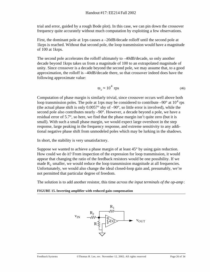
The solution is to add another resistor, this time across the input terminals of the op-amp :
FIGURE 15. Inverting amplifier with reduced gain compensation
This connection may be puzzling to those who have been taught to treat an op-amp as an ideal element whose input voltage difference is zero (the “virtual ground” concept and all that). It is easy to jump to the incorrect conclusion that the addition of a resistance in such a place cannot have any effect because the voltage across it is ideally zero. The key word is “ideally,” since we do not have an ideal op-amp. Consider, for example, placing a short circuit across the input terminals of the op-amp. The loop transmission must go to very small (zero) values in that situation.
Looking at the situation more analytically, note that such an additional resistor appears in parallel with R2 as far as the loop transmission is concerned, but disappears as far as the ideal closed-loop transfer function is concerned (this is where we invoke the virtual ground idea). Hence, we can effect changes in stability without disturbing the ideal closed-loop transfer function.
Let’s now compute how much gain reduction we need. Since the phase margin goal is 45°, we need to find the frequency at which –L(s) gives us a phase shift of –135°, since that will become the new crossover frequency.
Again, from inspection of the expression for the loop transmission, it should be apparent that the new crossover frequency should be the frequency of the second pole, that is, 103 rps, since at that frequency, the first pole has contributed essentially –90°, while the sec-ond pole contributes another –45°.
At the new desired crossover frequency, the uncompensated loop transmission has a mag-nitude of approximately:
(47)
Therefore, this is the factor by which we need to reduce the loop transmission gain.
The old loop transmission may be expressed as follows:
where the term in parentheses may be considered the compensator’s transfer function C(s).
Since we need to provide a whopping factor of 70.7 gain reduction, we need C(s) to have a value of 1/70.7. Therefore, we need to choose R small enough to give us this attenuation. Because of the large attenuation factor, we would expect R to be so small compared with R1 and R2 that it should be about 70.7 times smaller than R2, to a good approximation.
A slightly more rigorous calculation yields a value quite close to that estimate:
(51)
Summarizing, the reduced gain compensator has taken the system from a phase margin of about 5.7° to a phase margin of 45° by reducing the loop transmission by a factor of about 70.7 at all frequencies. At the same time, crossover has decreased by a factor of ten, from a frequency of 104 rps to 103 rps. The ideal closed-loop gain remains –99.
The trade-offs, of course, are a reduction in bandwidth and desensitivity. Furthermore, the reduction in desensitivity occurs at all frequencies, while stability is determined by just the behavior near crossover (so says phase margin, anyway). Hence, DC and low frequency desensitivity are apparently needlessly compromised by using such a simple-minded com-pensation scheme.
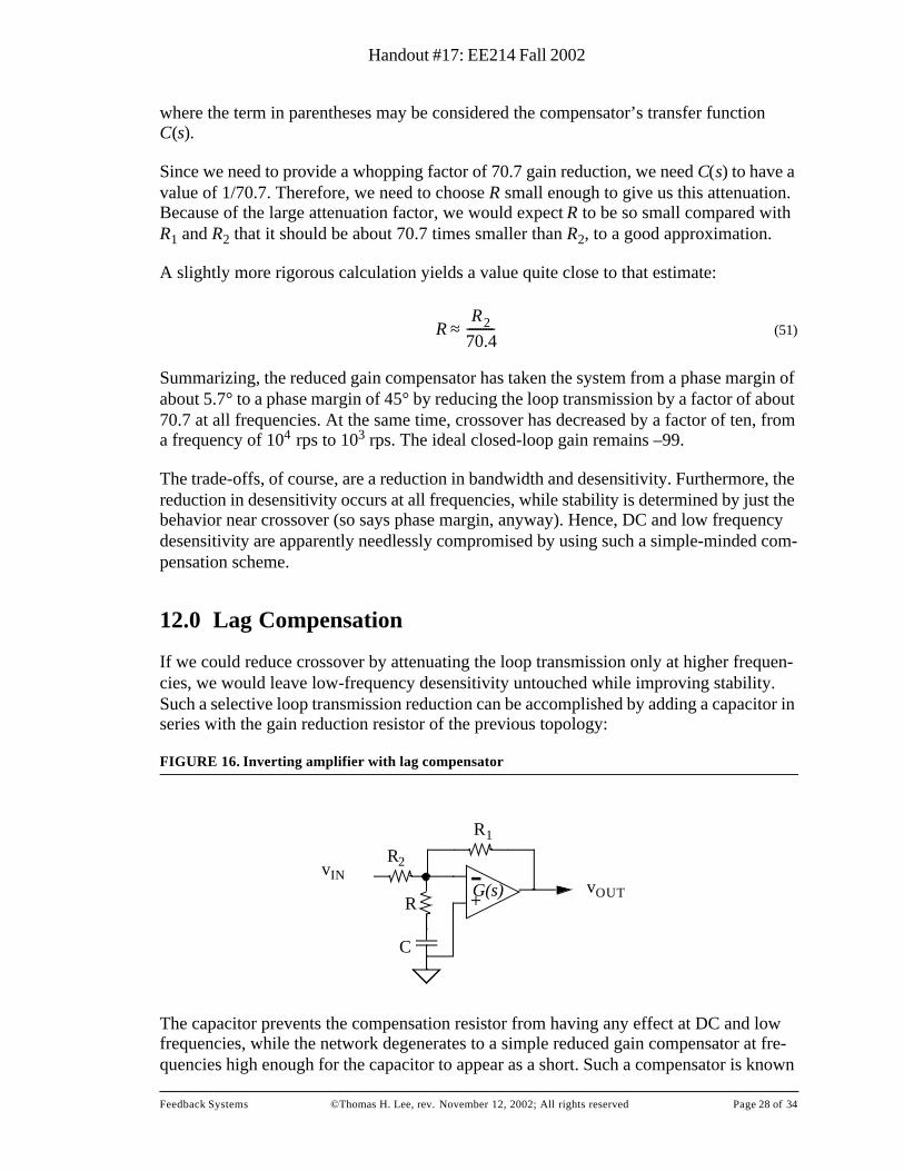
12.0 Lag Compensation
If we could reduce crossover by attenuating the loop transmission only at higher frequen-cies, we would leave low-frequency desensitivity untouched while improving stability. Such a selective loop transmission reduction can be accomplished by adding a capacitor in series with the gain reduction resistor of the previous topology:
FIGURE 16. Inverting amplifier with lag compensator
The capacitor prevents the compensation resistor from having any effect at DC and low frequencies, while the network degenerates to a simple reduced gain compensator at fre-quencies high enough for the capacitor to appear as a short. Such a compensator is known
as a lag compensator for reasons that will become clear shortly. Once again, the compen-sation network has no effect on the ideal closed-loop transfer function because it is con-nected across two terminals that have no voltage difference in the ideal limit of infinite op-amp gain.
To discover the real effect of this compensator, though, let’s derive an expression for the loop transmission:
(52)
which, after some manipulation, “simplifies” to:
(53)
which, after further manipulation, can be expressed in a somewhat more intuitively useful form:
(54)
The term in parentheses may be considered the transfer function of the compensator, while the rest of the equation is (minus) the loop transmission of the uncompensated system.
At DC, the compensator transfer function is unity, and the system behaves as in the uncompensated case. At very high frequencies, the compensator asymptotically approaches a value of:
(55)
just as in the reduced gain compensator case, as expected.
Note that the compensator C(s) contains one zero and one pole. As can be seen from the full expression for C(s), the pole is always at a lower frequency than the zero. It is the pole that causes the loop transmission magnitude to decrease (since the magnitude of C(s) decreases beyond the pole frequency). Unfortunately, an unavoidable side effect is the negative phase shift that is associated with the pole. It is this phase lag that gives this com-pensator its name.
L s( )–R1
R2 R 1sC------+
||---------------------------------- 1+
1–
G s( )⋅=
L s( )– sRC 1+
sC R 1R1
R2------+
R1+ 1R1
R2------+
+----------------------------------------------------------------------------- G s( )⋅=
L s( )– sRC 1+sC R R1 R2||+[ ] 1+-------------------------------------------------
Clearly, one important design criterion is to make sure that this lagging phase shift has been cancelled by the zero’s positive phase shift well below crossover, otherwise phase margin will actually degrade rather than improve.
A simple (but not necessarily optimum) design procedure is to begin with the reduced gain compensator to discover the value of R necessary to force crossover to a low enough fre-quency to achieve the specified phase margin. For reasons that will become clear shortly, it may be advisable to aim for a phase margin about 5 or 6 degrees larger than you ulti-mately want. Then, place the zero a decade below the new desired crossover by choosing
(56)
With this choice of zero location, the positive phase shift of the zero will be about 5.7° shy of its maximum, while the pole, with its lower frequency, has contributed just about all of its –90° of phase shift. Hence, if the reduced gain compensator is used as a starting point for lag compensator design, the phase margin goal should be augmented by 5 or 6 degrees, as stated earlier.
A more thoughtful design might require iteration to complete, since the pole and zero location are both adjustable parameters. Hence, there is no unique set of R and C that pro-vides a given phase margin. The simplified procedure presented here usually suffices, however, either to provide a final design, or to provide a reasonable initial design from which further optimization may develop.
The lag compensator provides roughly the same crossover (and hence, roughly the same closed-loop bandwidth) as the reduced gain compensator, but leaves the low-frequency loop transmission untouched. Hence, it doesn’t degrade desensitivity unnecessarily, and one may obtain all of the associated benefits, such as reduced steady-state step response error.
However, there is one drawback to the lag compensator that deserves mention. The com-pensator employs a zero that is well below crossover. Furthermore, since the ideal closed-loop transfer function does not contain a zero, our modeling procedure tells us that the zero must come from the forward path, and therefore, the zero appears in the closed-loop transfer function. Additionally, from root locus construction rules, we know that zeros are the terminal locations for loci; they attract poles. Hence, we expect a closed-loop pole close to this closed-loop low frequency zero. Therefore, poles being the natural frequen-cies of a network, there will be a slow-settling component to transient responses.13 The problem is equivalent to considering the effect of imperfect pole-zero cancellation.
To explore this idea in more detail, let us examine an isolated pole-zero doublet:
(57)
13. Here, “slow” means with respect to the crossover frequency.
To go further, we’ll need to recall the initial and final value theorems from Laplace trans-form theory:
(58)
(59)
With these formulas, it is straightforward to show that the initial value of the step response of a doublet is just α, while the final value is unity. Note that the initial value is not zero because the high-frequency gain does not go to zero (in fact, it goes to α).
Now that we know that the initial and final values are different, we next have to find how we get from the initial to the final value. Formally, one would use the inverse Laplace transform to discover this information rigorously. However, we can avoid a little labor by reflecting once again on the meaning of the term “natural frequency.” Evidently, then, the step response evolves exponentially from its initial to final value with a time constant equal to that of the pole.14
Returning to our specific case of the lag compensator, there is a pole-zero doublet formed by the compensating zero and its associated closed-loop pole. Because the zero is well below crossover, the doublet’s pole has a much slower time constant than the inverse loop bandwidth. Hence, settling to fine accuracy can be much slower than suggested by the loop bandwidth when a lag compensator is used.
13.0 Lead Compensation
We’ve seen that phase margin can be improved by reducing the magnitude of the loop transmission to lower the crossover frequency. The trade-offs with such an approach include a loss of desensitivity, and the possibility of low-frequency doublet formation.
An alternative compensation method is to alter the phase of the loop transmission, rather than its magnitude. That is, we wish to add a positive or leading phase shift near crossover to improve phase margin.
One method for doing so in our op-amp example is as follows:
14. This key fact is evidently poorly understood by many. The pole-zero separation determines the ratio of initial to final values, while only the pole determines the rate at which the response settles to the final value from the initial one. The zero thus has nothing to do with the time constant that describes the settling.
FIGURE 17. Inverting amplifier with lead compensator
Note that we are no longer maintaining the same ideal closed-loop transfer function. How-ever, as we’ll see, the overall closed-loop behavior will generally approach the desired ideal more closely than the reduced gain or lag compensated systems.
First, without writing any equations, let’s see how the addition of this capacitor should give us a loop transmission zero. As frequency increases, the transmission through the capacitor increases. That’s what a zero does, so we get a zero, as advertised. If we choose the capacitor value correctly, we can use the associated zero to bend the phase shift to more positive values and thereby increase phase margin.
There is one danger, however. A zero provides an increasing magnitude characteristic in addition to its positive phase shift. Hence, it also pushes out crossover. Therefore, there is the unfortunate possibility that a poorly placed zero will increase crossover so much that the positive phase shift of the zero will not offset the increased negative phase shift of the uncompensated system. The net effect could actually be a reduction in phase margin, so beware of this possibility.
Okay, now it’s time for an equation or two. Let’s derive an expression for the loop trans-mission for our lead-compensated system:
(60)
which may be expressed as:
(61)
Here, we see that the loop transmission zero is at a lower frequency than the associated pole, the opposite of the lag compensator.
+-R1
R2
vOUT
vING(s)
C
L s( )–R2
R2 R11
sC------||+
------------------------------- G s( )⋅=
L s( )–sR1C 1+
s R1 R2||( )C 1+--------------------------------------
Designing a lead compensator almost always involves a fair amount of iteration. A few hints may help constrain the search space, however. A reasonable starting point is to place the zero at the uncompensated system’s crossover frequency. Vary the zero location about this frequency and find the maximum. If the phase margin specification can be met, you’re finished.
Not infrequently, however, you find that the phase margin specification cannot be reached for any value of zero location. In such cases, a combination of gain reduction and lead compensation usually suffices. Unfortunately, with two varying parameters (gain reduc-tion and zero location), finding an optimum can be a bit involved, and machine computa-tion is definitely a tremendous help. Don’t turn off your brain, though -- you should always have a rough idea of what the answer should be, just as a sanity check on the com-puter’s results.
If the necessary gain reduction is too large, then convert the gain reduction into a lag net-work. The resulting lead-lag compensator then gives you maximum desensitivity at DC and at high frequencies.
At this point, you may be wondering how we can get away from the doublet problem that afflicts the lag compensator. The answer is two-fold. First, recognize that the lead zero is located near crossover, not well below it. Hence, any closed-loop pole that would be asso-ciated with it would have a time constant consistent with the loop bandwidth. That is, any doublet “tail” would settle out at about the same rate as the risetime, and hence would be invisible. This observation applies to all lead-compensated systems.
A second reason that applies specifically to the particular op-amp connection shown here is that the lead zero does not appear in the forward path. Again, to conclude that this must be the case, recognize that the ideal closed-loop transfer function involves a pole. Hence, the feedback block in our model must supply the zero. The forward gain block does not have a zero. Since the zero appears in the feedback path, it does not show up in the closed-loop transfer function, and therefore, there is no closed-loop doublet.
A question that often arises at this point is why anyone would ever use anything but a lead compensator. After all, it can actually provide greater bandwidth than the uncompensated system and it’s free of this doublet problem. The answer is that bandwidth costs power, and sometimes the price is too high. This consideration is particularly significant in mechanical systems where power requirements are roughly proportional to the cube of bandwidth.15 In large, industrial machinery, such a relationship between power and band-width favors the minimum bandwidth consistent with getting the job done.
Even in electronic systems, larger bandwidths are not always desirable. Noise is always present, and larger bandwidth can mean additional noise. If the bandwidth is in excess of
15. Here’s a quick handwaving “derivation” (put on your windbreakers, ‘cause we’re going to do a lot of handwaving): Power = work/time = (k1)(inertia)(angular acceleration/time) = (k2)(inertia)(ω2)/time = k3ω3. I warned you.
what is actually needed, then there is generally an unnecessary degradation of signal-to-noise ratio. In many instances, such a degradation is not tolerable.
14.0 Summary and Concluding Remarks
We’ve seen three basic compensation techniques that may be used individually or in com-bination. Both the reduced gain and lag compensators seek to improve phase margin by reducing crossover to a value where the corresponding phase shift is less negative than in the uncompensated case, thereby increasing phase margin.
The lag compensator improves on the simple reduced gain compensator by leaving untouched the low-frequency loop transmission, but introduces a potentially bothersome doublet that causes slow settling to high accuracy.
The lead compensator improves phase margin by directly improving the phase shift of the loop transmission. In so doing, the bandwidth actually increases. Furthermore, the doublet problem disappears because the pole associated with it is just as fast as the overall ampli-fier, so any “tail” in the response is effectively masked during the risetime.
The lead compensator frequently must be combined with either a reduced-gain or lag compensator to provide sufficient degrees of freedom to satisfy a given phase margin specification.
As a final note on compensation, it should be stated that the types discussed here do not comprise an exhaustive list. Additionally, even though these compensators were illus-trated with specific op-amp circuits, the fundamental notions apply to all other feedback systems as well. Hence, any method that reduces the loop transmission magnitude uni-formly is a reduced gain compensator, anything that introduces a loop transmission pole-zero pair in which the pole is at the lower frequency is a lag compensator, and so on.