Fiber-based cryogenic and time-resolvedspectroscopy of PbS quantum dots
Matthew T. Rakher,1,∗ Ranojoy Bose,2,3 Chee Wei Wong,2 and KartikSrinivasan1
1Center for Nanoscale Science and Technology, National Institute of Standards andTechnology, Gaithersburg, Maryland 20899-6203, USA
2Optical Nanostructures Laboratory, Center for Integrated Science and Engineering,Solid-State Science and Engineering and Mechanical Engineering, Columbia University, New
York, New York 10027, USA3Current Address: Institute for Research in Electronics and Applied Physics, University of
Abstract: PbSquantum dots are promising active emitters for use withhigh-quality Si nanophotonic devices in the telecommunications-band.Measurements of low quantum dot densities are limited both because of lowfluorescence levels and the challenges of single photon detection at thesewavelengths. Here, we report on methods using a fiber taper waveguideto efficiently extract PbS quantum dot photoluminescence. Temperaturedependent ensemble measurements reveal an increase in emitted photonsconcomitant with an increase in excited-state lifetime from 58.9 ns at293 K to 657 ns at 40 K. Measurements are also performed on quantumdots on high-Q(> 105) microdisks using cavity-resonant, pulsed excitation.
OCIS codes: (300.6280) Spectroscopy, fluorescence and luminescence; (230.5590) Quantum-well, -wire and -dot devices; (250.5230) Photoluminescence.
References and links1. F. Wise, “Lead salt quantum dots: the limit of strong quantum confinement,” Acc. Chem. Res.33, 773–780
(2000).2. Y. Takahashi, Y. Tanaka, H. Hagino, T. Sugiya, Y. Sato, T. Asano, and S. Noda, “Design and demonstration of
high-Q photonic heterostructure nanocavities suitable for integration,” Opt. Express17, 18093–18102 (2009).3. K. Srinivasan, P. E. Barclay, M. Borselli, and O. Painter, “Optical-fiber-based measurement of an ultrasmall
volume, high-Qphotonic crystal microcavity,” Phys. Rev. B70, 081306R (2004).4. S. Strauf, K. Hennessy, M. T. Rakher, Y.-S. Choi, A. Badolato, L. C. Andreani, E. L. Hu, P. M. Petroff, and
D. Bouwmeester, “Self-tuned quantum dot gain in photonic crystal lasers,” Phys. Rev. Lett.96, 127404 (2006).5. J. Raimond, M. Brune, and S. Haroche, “Manipulating quantum entanglement with atoms and photons in a
cavity,” Rev. Mod. Phys.73, 565–582 (2001).6. K. Srinivasan and O. Painter, “Linear and nonlinear optical spectroscopy of a strongly coupled microdisk-
quantum dot system,” Nature450, 862–865 (2007).7. M. T. Rakher, N. G. Stoltz, L. A. Coldren, P. M. Petroff, and D. Bouwmeester, “Externally mode-matched cavity
quantum electrodynamics with charge-tunable quantum dots,” Phys. Rev. Lett.102, 097403 (2009).8. C. Michael, K. Srinivasan, T. Johnson, O. Painter, K. Lee, K. Hennessy, H. Kim, and E. Hu, “Wavelength- and
material-dependent absorption in GaAs and AlGaAs microcavities,” Appl. Phys. Lett.90, 051108 (2007).9. A. Polman, “Erbium implanted thin film photonic materials,” J. Appl. Phys.82, 1–39 (1997).
10. H. Park, A. Fang, S. Kodama, and J. Bowers, “Hybrid silicon evanescent laser fabricated with a silicon waveguideand III-V offset quantum well,” Opt. Express13, 9460–9464 (2005).
11. E. H. Sargent, “Infrared quantum dots,” Adv. Mater. (Weinheim, Ger.)17, 515–522 (2004).
#138941 - $15.00 USD Received 30 Nov 2010; revised 10 Jan 2011; accepted 10 Jan 2011; published 14 Jan 2011(C) 2011 OSA 31 January 2011 / Vol. 19, No. 3 / OPTICS EXPRESS 1786
12. J. S. Steckel, S. Coe-Sullivan, V. Bulovic, and M. G. Bawendi, “1.3µm to 1.55µm Tunable electroluminescencefrom PbSe quantum dots embedded within an organic device,” Adv. Mater. (Weinheim, Ger.)15, 1862–1866(2003).
13. R. H. Hadfield, “Single-photon detectors for optical quantum information applications,” Nat. Photonics3, 696–705 (2009).
14. I. Fushman, D. Englund, and J. Vuckovic, “Coupling of PbS quantum dots to photonic crystal cavities at roomtemperature,” Appl. Phys. Lett.87, 241102 (2005).
15. Z. Wu, Z. Mi, P. Bhattacharya, T. Zhu, and J. Xu, “Enhanced spontaneous emission at 1.55 mu m from colloidalPbSe quantum dots in a Si photonic crystal microcavity,” Appl. Phys. Lett.90, 171105 (2007).
16. A. G. Pattantyus-Abraham, H. Qiao, J. Shan, K. A. Abel, T.-S. Wang, F. C. J. M. van Veggel, and J. F. Young,“Site-selective optical coupling of PbSe nanocrystals to Si-based photonic crystal microcavities,” Nano Lett.9,2849 (2009).
17. R. Bose, J. Gao, J. F. McMillan, A. D. Williams, and C. W. Wong, “Cryogenic spectroscopy of ultra-low densitycolloidal lead chalcogenide quantum dots on chip-scale optical cavities towards single quantum dot near-infraredcavity QED,” Opt. Express17, 22474–22483 (2009).
18. M. T. Rakher, R. Bose, C. W. Wong, and K. Srinivasan, “Spectroscopy of 1.55µm PbS quantum dots on Siphotonic crystal cavities with a fiber taper waveguide,” Appl. Phys. Lett.96, 161108 (2010).
19. Purchased from Evident Technologies and identified in this paper to foster understanding, without implyingrecommendation or endorsement by NIST.
20. F. Le Kien, S. Dutta Gupta, V. I. Balykin, and K. Hakuta, “Spontaneous emission of a cesium atom near ananofiber: Efficient coupling of light to guided modes,” Phys. Rev. A72, 032509 (2005).
21. M. Davanco and K. Srinivasan, “Efficient spectroscopy of single embedded emitters using optical fiber taperwaveguides,” Opt. Express17, 10542–10563 (2009).
22. K. Nayak, P. Melentiev, M. Morinaga, F. Kien, V. Balykin, and K. Hakuta, “Optical nanofiber as an efficient toolfor manipulating and probing atomic fluorescence,” Opt. Express15, 5431–5438 (2007).
23. M. Gregor, A. Kuhlicke, and O. Benson, “Soft-landing and optical characterization of a preselected single fluo-rescent particle on a tapered optical fiber,” Opt. Express17, 24234–24243 (2009).
24. E. Vetsch, D. Reitz, G. Sague, R. Schmidt, S. T. Dawkins, and A. Rauschenbeutel, “Optical interface createdby laser-cooled atoms trapped in the evanescent field surrounding an optical nanofiber,” Phys. Rev. Lett.104,203603 (2010).
25. L. Turyanska, A. Patane, M. Henini, B. Hennequin, and N. R. Thomas, “Temperature dependence of the photo-luminescence emission from thiol-capped PbS quantum dots,” Appl. Phys. Lett.90, 101913 (2007).
26. C. B. Layne, W. H. Lowdermilk, and M. J. Weber, “Multiphonon relaxation of rare-earth ions in oxide glasses,”Phys. Rev. B16, 10–20 (1977).
27. R. Bose, J. F. McMillan, J. Gao, K. M. Rickey, C. J. Chen, D. V. Talapin, C. B. Murray, and C. W. Wong,“Temperature-tuning of near-infrared monodisperse quantum dot solids at 1.5µm for controllable Forster energytransfer,” Nano Lett.8, 2006–2011 (2008).
28. M. T. Rakher, L. Ma, O. Slattery, X. Tang, and K. Srinivasan, “Quantum transduction of telecommunications-band single photons from a quantum dot by frequency upconversion,” Nat. Photonics4, 786–791 (2010).
29. I. Chung and M. G. Bawendi, “Relationship between single quantum-dot intermittency and fluorescence intensitydecays from collections of dots,” Phys. Rev. B70, 165304 (2004).
30. J. M. Pietryga, D. J. Werder, D. J. Williams, J. L. Casson, R. D. Schaller, V. I. Klimov, and J. A. Hollingsworth,“Utilizing the lability of lead selenide to produce heterostructured nanocrystals with bright, stable infrared emis-sion,” J. Am. Chem. Soc.130, 4879–4885 (2008).
31. M. J. Stevens, R. H. Hadfield, R. E. Schwall, S. W. Nam, R. P. Mirin, and J. A. Gupta, “Fast lifetime measure-ments of infrared emitters using a low-jitter superconducting single-photon detector,” Appl. Phys. Lett.89,031109 (2006).
1. Introduction
Lead-saltcolloidal quantum dots (QDs) [1] such as PbS QDs are interesting active emittersdue to the fact that they can be integrated with high quality, Si-based nanophotonic devicesdesigned to operate near 1550 nm [2, 3]. These devices can potentially be used for applicationssuch as ultra-low threshold lasers [4] as well as fundamental studies of light-matter interaction[5]. While significant strides along these lines have been made with self-assembled InAs QDsembedded in GaAs-based devices [6, 7], the optical quality factors (Qs) obtained are usuallyan order of magnitude lower [8] than what can be achieved in Si, SiO2, or SiN [2]. In addition,the fabrication of electronic and micromechanical systems in Si-based materials is much moremature than in GaAs. Thus, the introduction of an active emitter with Si-based optical micro-
#138941 - $15.00 USD Received 30 Nov 2010; revised 10 Jan 2011; accepted 10 Jan 2011; published 14 Jan 2011(C) 2011 OSA 31 January 2011 / Vol. 19, No. 3 / OPTICS EXPRESS 1787
cavities and waveguides is a very active field of research [9, 10]. In contrast to InAs quantumdots,PbS QDs have longer radiative lifetimes by 2 to 3 orders of magnitude [11] and reducedquantum efficiencies by 1 to 2 orders of magnitude when dried [12], yielding a photon emis-sion rate that is as much as five orders of magnitude worse. Combined with the challenges ofsingle-photon detection in the near-infrared [13], performing spectroscopic measurements oflow densities of PbS QDs can be difficult and photon collection efficiencies must be as high aspossible.
Previous work [14, 15, 16, 17] with lead-salt QDs on microcavities has focused on usingfree-space optics and microscope objectives to collect emission, but this is limited by the pla-nar geometry of the microcavities. Recently, it was shown that coupling to photonic crystalcavities through a fiber taper waveguide is an efficient method to extract emitted photons[18]. In addition, it was demonstrated that the QDs did not degrade theQ of the cavity upto Q ≈ 3×10⁴. Here, we present further spectroscopic techniques for PbS QDs based upon ef-ficient collection using a fiber taper waveguide (FTW) [3]. In particular, we perform cryogenicphotoluminescence (PL) studies of low-densities of QDs dried directly onto an FTW, enablingefficient measurement in a range of environmental conditions. Also, we demonstrate PL andtime-resolved PL measurements of QDs dried onto Si microdisk cavities and show thatQs upto 105 are unaffected by the QDs. As discussed in the last section of this letter, single PbS QDmeasurements, like those performed on InAs QDs, will be quite challenging due to the afore-mentioned detection difficulties and use of the techniques described here will be necessary tomake such experiments more feasible.
2. Experimental Setup
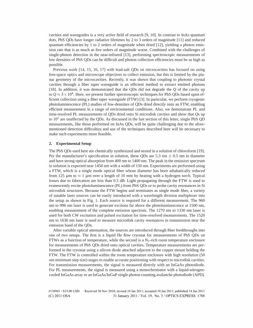
The PbS QDs used here are chemically synthesized and stored in a solution of chloroform [19].Per the manufacturer’s specification in solution, these QDs are 5.3 nm± 0.5 nm in diameterand have strong optical absorption from 400 nm to 1400 nm. The peak in the emission spectrumin solution is expected near 1450 nm with a width of 150 nm. Experiments are performed usinga FTW, which is a single mode optical fiber whose diameter has been adiabatically reducedfrom 125µm to ≈ 1 µm over a length of 10 mm by heating with a hydrogen torch. Typicallosses due to fabrication are less than 0.5 dB. Light propagating through the FTW is used toevanescently excite photoluminescence (PL) from PbS QDs or to probe cavity resonances in Simicrodisk structures. Because the FTW begins and terminates as single mode fiber, a varietyof tunable laser sources can be easily introduced with a wavelength division multiplexer intothe setup as shown in Fig. 1. Each source is required for a different measurement. The 960nm to 996 nm laser is used to generate excitons far above the photoluminescence at 1500 nm,enabling measurement of the complete emission spectrum. The 1270 nm to 1330 nm laser isused for both CW excitation and pulsed excitation for time-resolved measurements. The 1520nm to 1630 nm laser is used to measure microdisk cavity resonances in transmission near theemission band of the QDs.
After variable optical attenuation, the sources are introduced through fiber feedthroughs intoone of two setups. The first is a liquid He flow cryostat for measurements of PbS QDs onFTWs as a function of temperature, while the second is a N2-rich room temperature enclosurefor measurements of PbS QDs dried onto optical cavities. Temperature measurements are per-formed in the cryostat using a silicon diode attached adjacent to the copper mount holding theFTW. The FTW is controlled within the room temperature enclosure with high resolution (50nm minimum step size) stages to enable accurate positioning with respect to microdisk cavities.For transmission measurements, the signal is measured directly with an InGaAs photodiode.For PL measurements, the signal is measured using a monochromator with a liquid-nitrogen-cooled InGaAs array or an InGaAs/InGaP single photon counting avalanche photodiode (APD).
#138941 - $15.00 USD Received 30 Nov 2010; revised 10 Jan 2011; accepted 10 Jan 2011; published 14 Jan 2011(C) 2011 OSA 31 January 2011 / Vol. 19, No. 3 / OPTICS EXPRESS 1788
1270-1330 nm
Tunable Laser
960-996 nm
Tunable Laser
IR Spectrometer
InGaAs
CCD
LHe cryostat
disk
EOM
APD
Variable
Delay
Pulse GeneratorSYNCOUT
VOA
WDM
1520-1630 nm
Tunable Laser
PDTrans
FTW
Fig. 1. Experimental setup composed of tunable-wavelength laser sources (980 nm, 1310nm, and 1550 nm), electro-optic intensity modulator (EOM), wavelength division mul-tiplexer (WDM), variable optical attenuator (VOA), fiber taper waveguide (FTW), cryo-stat, timing electronics, and measurement devices (spectrometer, photodiode (PD), and In-GaAs/InGaP single photon counting avalanche photodiode (APD)).
The pulsed source near 1300 nm required for time-resolved measurements is created using anelectro-optic intensity modulator driven by a pulse generator. These instruments combine tocreate wavelength-tunable (1300 nm to 1320 nm) 22.8 fJ, 2.1 ns pulses at a user-defined rep-etition rate of 1 KHz to 1 MHz with an on/off extinction ratio of 28.1 dB. It is important tonote that the EOM-based pulsed excitation offers substantial flexibility in repetition rate, wave-length, and pulse length compared to most pulsed laser systems. Using a faster pulse generatorit would be possible to create pulses as short as 100 ps, making future Purcell effect measure-ments possible. Because the APD must run in a gated-detection mode, the detection gate issynchronized to the arrival of the optical pulse with a delay generator triggered by the pulsegenerator as shown in Fig. 1. Time-resolved measurements are accomplished by changing thedelay of the APD gating with respect to the arrival of the PL pulse and integrating the counts fora specified time. If the expected decay times were shorter than the width of the APD gate (100ns maximum), the measurement could be performed in a multi-channel way using a standardtime-correlated counting board.
3. Cryogenic and Time-resolved Measurements of PbS QDs dried on FTW
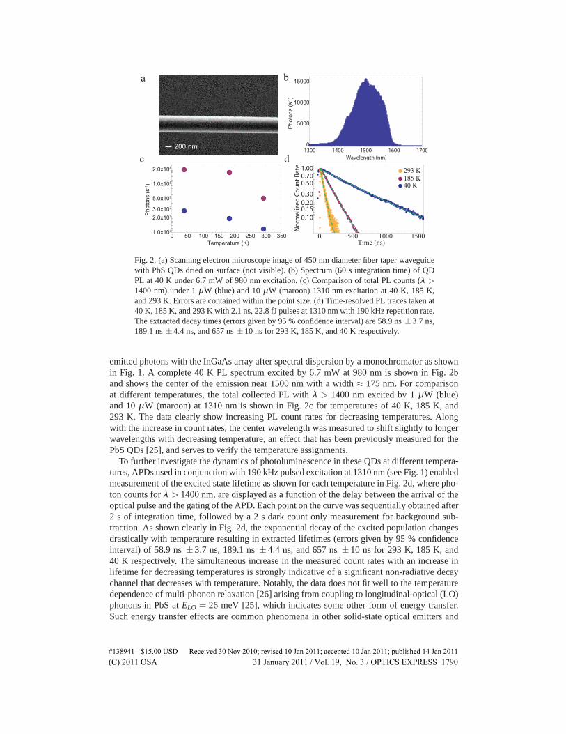
In the first set of measurements, PbS QDs in chloroform solution are diluted to a concentrationof 0.5 mg/mL. Then,≈10µL drops are dried on a glass slide overlayed with the FTW, resultingin a low density (≈1000µm−2 as measured by scanning electron microscopy) drying onto theFTW. Previous theoretical [20, 21] and experimental work [22, 23, 24] has shown that FTWscan be efficient channels for the collection of spontaneous emission from nearby, optically-active sources such as atoms, ions, or QDs. In fact, it was shown theoretically [20] that anoptimally-sized FTW of diameter≈ λ/4 could collect approximately 28 % of the total lightfrom a nearby emitter. In the experiments here, the FTW is used both for efficient evanescentexcitation and collection of subsequent PL. The FTW is tapered to a nearly-optimal diameterof ≈450 nm, see Fig. 2a, to optimize collection efficiency near 1500 nm while minimizingscattering loss. For the FTW shown in Fig. 2a, the loss induced by the tapering was≈5 dB,much more than for a diameter of 1µm (0.5 dB), and is due to a breakdown of adiabaticityat these small length scales. Given the areal density and the size of the FTW, the total numberof QDs that could interact with the propagating optical mode was≈ 106. The FTW with PbSQDs is loaded into the He-flow cryostat for PL measurements at 293 K, 185 K, and 40 K. PLspectroscopy is performed by exciting the PbS QDs at 980 nm or 1310 nm and measuring the
#138941 - $15.00 USD Received 30 Nov 2010; revised 10 Jan 2011; accepted 10 Jan 2011; published 14 Jan 2011(C) 2011 OSA 31 January 2011 / Vol. 19, No. 3 / OPTICS EXPRESS 1789
c d
0 500 1000 1500
0.10
1.00
0.50
0.20
0.30
0.15
0.70
Time (ns)
No
rma
liz
ed
Co
un
t R
ate 293 K
185 K40 K
200 nm
a b
0 50 100 150 200 250 300 3501.0x107
1.0x10⁸
5.0x10⁷
2.0x10⁷
2.0x10⁸
3.0x10⁷
Temperature (K)
Photo
ns (
s-1)
1300 1400 1500 1600 17000
5000
10000
15000
Wavelength (nm)
Ph
oto
ns (
s-1)
Fig. 2. (a) Scanning electron microscope image of 450 nm diameter fiber taper waveguidewith PbS QDs dried on surface (not visible). (b) Spectrum (60 s integration time) of QDPL at 40 K under 6.7 mW of 980 nm excitation. (c) Comparison of total PL counts (λ >1400 nm) under 1µW (blue) and 10µW (maroon) 1310 nm excitation at 40 K, 185 K,and 293 K. Errors are contained within the point size. (d) Time-resolved PL traces taken at40 K, 185 K, and 293 K with 2.1 ns, 22.8 fJ pulses at 1310 nm with 190 kHz repetition rate.The extracted decay times (errors given by 95 % confidence interval) are 58.9 ns±3.7 ns,189.1 ns±4.4 ns, and 657 ns±10 ns for 293 K, 185 K, and 40 K respectively.
emitted photons with the InGaAs array after spectral dispersion by a monochromator as shownin Fig. 1. A complete 40 K PL spectrum excited by 6.7 mW at 980 nm is shown in Fig. 2band shows the center of the emission near 1500 nm with a width≈ 175 nm. For comparisonat different temperatures, the total collected PL withλ > 1400 nm excited by 1µW (blue)and 10µW (maroon) at 1310 nm is shown in Fig. 2c for temperatures of 40 K, 185 K, and293 K. The data clearly show increasing PL count rates for decreasing temperatures. Alongwith the increase in count rates, the center wavelength was measured to shift slightly to longerwavelengths with decreasing temperature, an effect that has been previously measured for thePbS QDs [25], and serves to verify the temperature assignments.
To further investigate the dynamics of photoluminescence in these QDs at different tempera-tures, APDs used in conjunction with 190 kHz pulsed excitation at 1310 nm (see Fig. 1) enabledmeasurement of the excited state lifetime as shown for each temperature in Fig. 2d, where pho-ton counts forλ > 1400 nm, are displayed as a function of the delay between the arrival of theoptical pulse and the gating of the APD. Each point on the curve was sequentially obtained after2 s of integration time, followed by a 2 s dark count only measurement for background sub-traction. As shown clearly in Fig. 2d, the exponential decay of the excited population changesdrastically with temperature resulting in extracted lifetimes (errors given by 95 % confidenceinterval) of 58.9 ns±3.7 ns, 189.1 ns±4.4 ns, and 657 ns±10 ns for 293 K, 185 K, and40 K respectively. The simultaneous increase in the measured count rates with an increase inlifetime for decreasing temperatures is strongly indicative of a significant non-radiative decaychannel that decreases with temperature. Notably, the data does not fit well to the temperaturedependence of multi-phonon relaxation [26] arising from coupling to longitudinal-optical (LO)phonons in PbS atELO = 26 meV [25], which indicates some other form of energy transfer.Such energy transfer effects are common phenomena in other solid-state optical emitters and
#138941 - $15.00 USD Received 30 Nov 2010; revised 10 Jan 2011; accepted 10 Jan 2011; published 14 Jan 2011(C) 2011 OSA 31 January 2011 / Vol. 19, No. 3 / OPTICS EXPRESS 1790
1400 1450 1500 15500
500
1000
1500
2000
2500
3000
Wavelength (nm)
Photo
ns (
s-1)
1304.85 1304.95 1305.05 1305.15
0.2
0.4
0.6
0.8
1.0
Wavelength (nm)T
ran
sm
issio
n
0 100 200 300 400 5000
2000
4000
6000
8000
10000
Time (ns)
Co
un
ts
a b
c d
1520 1540 1560 1580 1600 1620
0.6
0.7
0.8
0.9
1.0
Wavelength (nm)
Tra
nsm
issio
n
1550.10 1550.20 1550.30100 nm
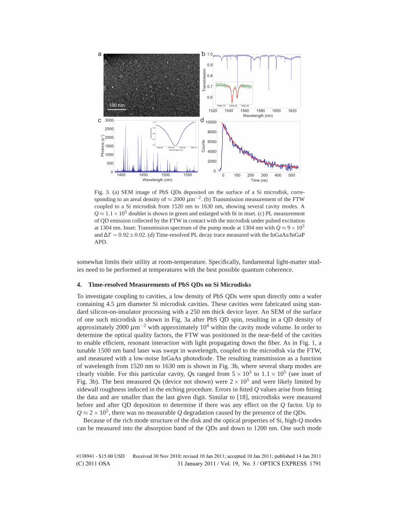
Fig. 3. (a) SEM image of PbS QDs deposited on the surface of a Si microdisk, corre-spondingto an areal density of≈ 2000µm−2. (b) Transmission measurement of the FTWcoupled to a Si microdisk from 1520 nm to 1630 nm, showing several cavity modes. AQ ≈ 1.1×10⁵ doublet is shown in green and enlarged with fit in inset. (c) PL measurementof QD emission collected by the FTW in contact with the microdisk under pulsed excitationat 1304 nm. Inset: Transmission spectrum of the pump mode at 1304 nm withQ ≈ 9×10³
and∆T = 0.92±0.02. (d) Time-resolved PL decay trace measured with the InGaAs/InGaPAPD.
somewhat limits their utility at room-temperature. Specifically, fundamental light-matter stud-ies need to be performed at temperatures with the best possible quantum coherence.
4. Time-resolved Measurements of PbS QDs on Si Microdisks
To investigate coupling to cavities, a low density of PbS QDs were spun directly onto a wafercontaining 4.5µm diameter Si microdisk cavities. These cavities were fabricated using stan-dard silicon-on-insulator processing with a 250 nm thick device layer. An SEM of the surfaceof one such microdisk is shown in Fig. 3a after PbS QD spin, resulting in a QD density ofapproximately 2000µm−2 with approximately 104 within the cavity mode volume. In order todetermine the optical quality factors, the FTW was positioned in the near-field of the cavitiesto enable efficient, resonant interaction with light propagating down the fiber. As in Fig. 1, atunable 1500 nm band laser was swept in wavelength, coupled to the microdisk via the FTW,and measured with a low-noise InGaAs photodiode. The resulting transmission as a functionof wavelength from 1520 nm to 1630 nm is shown in Fig. 3b, where several sharp modes areclearly visible. For this particular cavity,Qs ranged from 5× 10³ to 1.1× 10⁵ (see inset ofFig. 3b). The best measuredQs (device not shown) were 2× 10⁵ and were likely limited bysidewall roughness induced in the etching procedure. Errors in fittedQ values arise from fittingthe data and are smaller than the last given digit. Similar to [18], microdisks were measuredbefore and after QD deposition to determine if there was any effect on theQ factor. Up toQ ≈ 2×10⁵, there was no measurableQ degradation caused by the presence of the QDs.
Because of the rich mode structure of the disk and the optical properties of Si, high-Qmodescan be measured into the absorption band of the QDs and down to 1200 nm. One such mode
#138941 - $15.00 USD Received 30 Nov 2010; revised 10 Jan 2011; accepted 10 Jan 2011; published 14 Jan 2011(C) 2011 OSA 31 January 2011 / Vol. 19, No. 3 / OPTICS EXPRESS 1791
is shown in transmission in the inset of Fig.3c withQ ≈ 9×10³. The FTW enables efficientcoupling to this mode with coupling depth∆T = 0.92± 0.02, just short of critical coupling,ensuring almost complete transfer of power. By pumping on this mode, only QDs on the cir-cumference of the disk are excited by the circulating pump. The 1300 nm tunable laser com-bined with the EOM enable cavity-resonant pulsed excitation. Using 2.1 ns pulses at 1304 nm(resonant with the mode) with 1 MHz repetition rate, the QDs emit a PL signal under 79 nW ofaverage power as shown in the spectrum in Fig. 3c. The significant reduction in average powerrequired to obtain a bright PL spectrum is due to the buildup of power in the cavity mode. Inthe spectrum, the modes of the microdisk in the emission band are clearly visible and dress thebroad PL signal of the QDs. The significant difference between the spectrum in Fig. 3c com-pared to that of bulk QD emission (see Fig. 2b) verifies that the majority of the collected PL isemitted by QDs into the cavity modes at the circumference rather than directly into the FTWfrom QDs near to the center of the disk. Incorporation of the gated APD and requisite timingelectronics enables a time-resolved measurement of the PL decay as shown in Fig. 3d. Thelifetime extracted from this room-temperature measurement is 160 ns± 20 ns. This lifetime islonger than that measured for the QDs dried directly on the FTW at room-temperature, but is ofthe same order of magnitude. We measure markedly different room temperature excited statelifetimes for different samples which implies strong density-dependent or environmentally-dependent decay dynamics such as Forster resonant energy transfer (FRET) [27]. These effectsneed to be investigated further and will be the focus of future work.
5. Discussion and Conclusion
We have demonstrated techniques for efficient collection of photons emitted by PbS QDs inthe 1.5µm band using FTWs in different environments as well as on microdisk cavities. Usingthese collection strategies, it is an important exercise to consider if it is experimentally feasibleto detect the single photon emission from a single PbS QD in a lifetime measurement and ina Hanbury-Brown and Twiss setup, much like what is done with InAs QDs. In the collectiongeometries presented here, the fraction of spontaneous emission collected in the measurementmode should be on the order of 1 % to 28 % [20], neglecting any substantial Purcell enhance-ment. Coupled with assumed radiative lifetimes as long as 700 ns, photoluminescence photonrates from a single PbS QD should reach as high as≈ 2×10⁵ s−1 under saturated continuouswave excitation if the radiative efficiency at low temperature approaches unity. However, theseseemingly high count rates are mitigated by the difficulties of single photon detection in thenear-infrared [13]. In particular, for the InGaAs APD used in our experiments, the optimumdetection parameters for a single-channel lifetime measurement like that found in Fig. 2d andFig. 3d are a 20 % detection efficiency, 100 ns gate width, and 10µs dead time for a 1 MHztrigger rate. These settings have a dark count rate of≈ 1.7×10³ s−1, yielding a signal to noiseratio of≈35.4 Hz−1/2. Experimentally, this means that the excited-state decay will be observedwith a dynamic range of 35.4 if each temporal point is integrated for 1 s, corresponding to ameasurable decay over a time period of≈ 3.5 times the decay constant. Compared to an upcon-version, multi-channel Si APD measurement for InAs QDs, the dynamic range is approximatelya factor of 30 times worse [28].
More important than a lifetime measurement is that of the second order intensity correlationg2(τ), where
anda (a†) is the photon annihilation (creation) operator, which yields information about thenon-classicality of the emitted photon stream. Specifically, a measured value ofg(2)(0) < 0.5
#138941 - $15.00 USD Received 30 Nov 2010; revised 10 Jan 2011; accepted 10 Jan 2011; published 14 Jan 2011(C) 2011 OSA 31 January 2011 / Vol. 19, No. 3 / OPTICS EXPRESS 1792
proves that the field is dominantly composed of single photons. Using a standard Hanbury-Brown and Twiss setup, a minimum measurableg(2)(0) value for a PbS QD would be≈0.60using a 10 % detection efficiency, 2.5 ns gate width, and 10µs dead time for a 1 MHz triggerrate. While this is a reasonably low value (proving the field is non-classical but not single pho-ton), the signal to noise under these measurement conditions is only≈ 0.011 Hz−1/2, requiringmore than two hours of integration time to achieve unity signal to noise. A signal to noise of≈ 0.16 Hz−1/2 could be obtained by increasing the gate width to 50 ns, but the minimum mea-surableg(2)(0) under these conditions is≈ 0.81. In summary, under the best possible collectionconditions and assuming perfect radiative efficiency, it is not possible to measureg(2)(0)< 0.5using commercially available detectors. In addition, the assumption of perfect radiative effi-ciency does not match experimental observation, even at cryogenic temperatures. This couldbe caused by several factors including blinking [18, 29] and poor radiative efficiency out ofsolution [12]. Therefore, it appears that single QD measurements at these wavelengths may re-main elusive until higher optical quality QDs can be regularly fabricated [30]. However, oncethese QDs are realized, measurement of single photons will likely require advanced detectortechnologies such as frequency upconversion [28] or superconducting single photon detectors[31]. Nonetheless, the efficient and flexible measurement techniques presented here will beof great use towards the development of PbS QDs as active emitters coupled to high-qualitynanophotonic devices in the telecommunications-band.
Acknowledgements
The authors acknowledge fabrication support from D. L. Kwong and M. Yu at the Instituteof Microelectronics in Singapore, funding support from NSF ECCS 0747787, the NanoscaleScience and Engineering Initiative under NSF Award Number CHE-0641523, and the NewYork State Office of Science, Technology, and Innovation.
#138941 - $15.00 USD Received 30 Nov 2010; revised 10 Jan 2011; accepted 10 Jan 2011; published 14 Jan 2011(C) 2011 OSA 31 January 2011 / Vol. 19, No. 3 / OPTICS EXPRESS 1793