Field-effect at electrical contacts to two-dimensional materials Yao Guo1,2 (), Yan Sun1, Alvin Tang2, Ching-Hua Wang2, Yanqing Zhao1, Mengmeng Bai1, Shuting Xu1, Zheqi Xu1, Tao Tang3, Sheng Wang4, Chenguang Qiu4, Kang Xu5, Xubiao Peng1, Junfeng Han1, Eric Pop2, and Yang Chai5 ()
ABSTRACT The inferior electrical contact to two-dimensional (2D) materials is a critical challenge for their application in post-silicon very large- scale integrated circuits. Electrical contacts were generally related to their resistive effect, quantified as contact resistance. With a systematic investigation, this work demonstrates a capacitive metal-insulator-semiconductor (MIS) field-effect at the electrical contacts to 2D materials: The field-effect depletes or accumulates charge carriers, redistributes the voltage potential, and gives rise to abnormal current saturation and nonlinearity. On one hand, the current saturation hinders the devices’ driving ability, which can be eliminated with carefully engineered contact configurations. On the other hand, by introducing the nonlinearity to monolithic analog artificial neural network circuits, the circuits' perception ability can be significantly enhanced, as evidenced using a coronavirus disease 2019 (COVID-19) critical illness prediction model. This work provides a comprehension of the field-effect at the electrical contacts to 2D materials, which is fundamental to the design, simulation, and fabrication of electronics based on 2D materials.
1 Introduction The emergence of artificial intelligence and 5G communication requires electronics with greater computing performance and higher energy efficiency. With their abundance and the rich variety of electronic properties, the family of atomically thin two-dimensional (2D) materials is a promising choice in the next generation of very-large-scale-integration (VLSI) technology [1–4]. Electronics devices based on atomically thin 2D materials such as transition metal sulfides, black phosphorus, and graphene, have been intensively studied during the past decade. 2D material-based electronics show great potential for building both traditional von Neumann computing architecture and state-of-art non-von Neumann in-memory-computing architecture [5–17]. However, the inferior electrical contacts greatly hinder the performance of 2D material-based electronic devices [18–22]. The inferior electrical contacts are generally related to their significant resistive effect at the interface, quantified as the contact resistance [13]. Multiple elaborate methods have been developed to lower the contact resistance through engineering the metal-2D material interface, such as low work function metallization [23], defect and impurity control [24, 25], doping [26–29], phase change transition [30], and the recent van der Waals contacts [31–33]. Herein, continuous improvement of the electrical to 2D materials is required, and full fundamental
comprehension of the electrical contacts to 2D materials is substantially needed.
In previous researches, attention has been generally focused on the resistive effect at the electrical contact interface. In this research, we investigate the electrical contacts to 2D materials from a bottomed physical perspective and demonstrate that for the atomically thin 2D materials, the electrical contacts contribute not only the resistive effect but also a significant capacitive metal-insulator-semiconductor (MIS) field-effect. The capacitive MIS field-effect can deplete or accumulate the charge carriers, redistribute the voltage potential, and give rise to unusual current saturation and nonlinearity. Based on a thorough understanding, one can selectively decide whether to eliminate such field-effect or use it. On one hand, engineering the electrical contact configuration can eliminate the field-effect and significantly improve the driving current of the 2D material based transistors. On the other hand, the nonlinearity introduced by the electrical contact to 2D materials can efficiently improve the perceptron ability of the non-von Neumann in-memory-computing circuit, as demonstrated by a COVID-19 critical illness prediction model. The principle in this research generally applies to a wide range of 2D materials. The comprehension of the field-effect at electrical contacts facilitates the design, simulation, and fabrication of electronics based on 2D material.
www.theNanoResearch.com∣www.Springer.com/journal/12274 | Nano Research
4895
2 Results and discussion
2.1 Principle of the capacitive MIS field-effect at
electrical contact
For concision, we first expound on the general principle of the capacitive MIS field-effect. Figure 1(a) shows a simplified 2D material channel (monolayer MoS2, for example) with two contacting metallic electrodes. As shown in the inset, the sidewall of the metallic electrode, the insulating dielectric (or vacuum), and the semiconducting channel form a fringe metal- insulator-semiconductor (MIS) structure. At the ends of the channel, the distance between the metallic sidewall and the channel is small (Ångstroms to nanometers). The capacitive coupling between the metallic sidewall and the channel can be very effective. Therefore the voltage drop between the metallic sidewall and the channel (which is VM-S = IDS·RC, where IDS is the current and RC is the contact resistance) can create a significant MIS field-effect. As shown in Fig. S1(a) in the Electronic Supplementary Material (ESM), we simulated the simplified device (monolayer MoS2, n-type, donor density 6 × 1012 cm−2, intrinsic mobility 400 cm2·V−1·s−1, channel length 500 nm, and contact resistance 2RC = 1.3 kΩ) with technology computer- aided design (TCAD). Figure 1(b) and Fig. S1(b) in the ESM show the simulated electron density distribution in the channel. For VDS = 0 V, the electron density is inconsistent with the donor doping density. With applied VDS = 1 V, carriers deplete/ accumulate at the source/drain end of the channel. For increased VDS up to 5 V, the depletion/accumulation is further strengthened. The depletion/accumulation is due to the field-effect coupled through the MIS structure, where the voltage drop ±VM-S is applied between the source/drain electrode sidewall and the channel, respectively. The fully depleted region is non-conducting,
correspondingly, a considerable part of voltage potential drops on the depletion region, as shown in Fig. 1(c). Considering this capacitive MIS field-effect, we plot the equivalent circuit as shown in Fig. 1(d). Besides the source/drain contact resistors (RC) and the channel resistor (RCh), the circuit consists of two extra parasitic MIS field-effect transistors. The gates of the transistors correspond to the sidewalls of the electrodes. The IDS–VDS curves of the equivalent circuit with various contact/ channel resistances (2RC = RCh) are shown in Fig. 1(e), which are in good accordance with the TCAD simulated IDS–VDS curves of the constructed devices with various doping densities, as shown in Fig. 1(f). The current increases linearly with small VDS and saturates with large VDS. The current saturation results from a negative feedback mechanism: With increased VDS, the field-effect at the Source end can fully deplete the carriers through the atomically thin 2D material, dramatically decrease the conductivity, prevent the IDS from increasing, and in turn cause apparent current saturation. We further carry comparative simulations by replacing the source/drain with the virtual zero-thickness electrodes, as shown in Fig. S1(c) in the ESM. In this case, the fringe capacitive MIS field-effect coupling is absent. Consequently, we do not see the carrier depletion/ accumulation at the ends of the channel, as shown in Fig. 1(g) and Fig. S1(d) in the ESM. The voltage drop redistributes equably, and the I–V curves maintain good linearity, as shown in Figs. 1(h) and 1(i). The comparative simulations confirm the field-effect originated from the MIS structure. The zero-thickness virtual electrodes neglect the apparent field-effect at the electrical contact to 2D materials, which should be used with extra caution in TCAD simulations. Additionally, the field-effect for devices with various metal electrode thicknesses and channel thicknesses (layer number) is also investigated, as shown in Fig. S2 in the ESM.
Figure 1 Principle of the capacitive MIS field-effect. (a) Capacitive MIS field-effect of electrical contacts coupled through the MIS structure. (b) Electron density and (c) voltage potential along the MoS2 channel. (d) Equivalent circuit of devices considering the capacitive MIS field-effect. (e) IDS–VDS curves of the equivalent circuit. The legends are the contact/channel resistance (2RC = RCh). (f) IDS–VDS curves of the TCAD simulated device, the legends are the doping density (cm−2). (g) Electron density, (h) the voltage drop distribution, and (i) IDS–VDS curves of the device without the capacitive MIS field-effect.
Nano Res. 2021, 14(12): 4894–4900
| www.editorialmanager.com/nare/default.asp
4896
The above analysis has proposed a field-effect at the electrical contacts to 2D materials, which can significantly deplete/ accumulate carriers, change the voltage potential distribution, and give rise to apparent current saturation. For clarification, the above simulations have used the simplified device geometry with only one channel and two electrodes. However, the principle is universal and applies to practical 2D material devices with more complex geometries, as will be shown below. A similar analysis also applies to Schottky contacts, where the field-effect widens the Schottky barrier width at the contact area, blocks the field/thermal-field emission current, and causes a similar current saturation, as we specify detailedly in Section S3 in the ESM.
2.2 Capacitive MIS field-effect at the electrical contacts
to monolayer MoS2
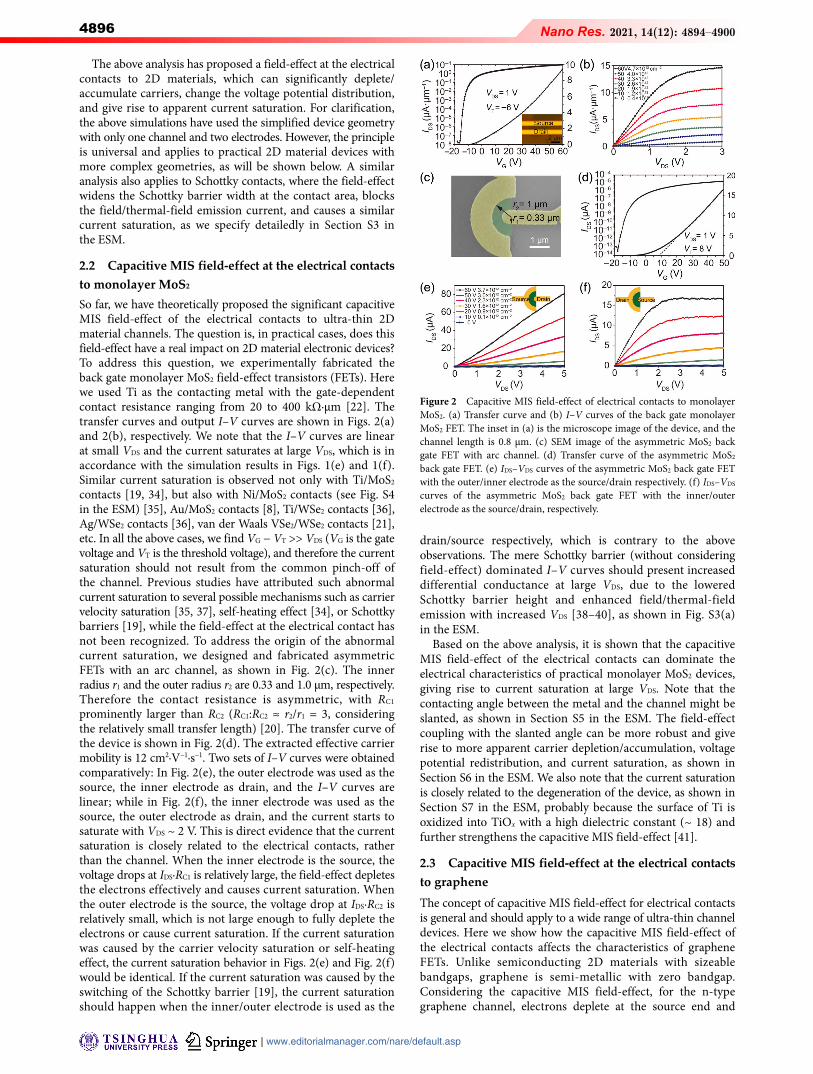
So far, we have theoretically proposed the significant capacitive MIS field-effect of the electrical contacts to ultra-thin 2D material channels. The question is, in practical cases, does this field-effect have a real impact on 2D material electronic devices? To address this question, we experimentally fabricated the back gate monolayer MoS2 field-effect transistors (FETs). Here we used Ti as the contacting metal with the gate-dependent contact resistance ranging from 20 to 400 kΩ·μm [22]. The transfer curves and output I–V curves are shown in Figs. 2(a) and 2(b), respectively. We note that the I–V curves are linear at small VDS and the current saturates at large VDS, which is in accordance with the simulation results in Figs. 1(e) and 1(f). Similar current saturation is observed not only with Ti/MoS2 contacts [19, 34], but also with Ni/MoS2 contacts (see Fig. S4 in the ESM) [35], Au/MoS2 contacts [8], Ti/WSe2 contacts [36], Ag/WSe2 contacts [36], van der Waals VSe2/WSe2 contacts [21], etc. In all the above cases, we find VG − VT >> VDS (VG is the gate voltage and VT is the threshold voltage), and therefore the current saturation should not result from the common pinch-off of the channel. Previous studies have attributed such abnormal current saturation to several possible mechanisms such as carrier velocity saturation [35, 37], self-heating effect [34], or Schottky barriers [19], while the field-effect at the electrical contact has not been recognized. To address the origin of the abnormal current saturation, we designed and fabricated asymmetric FETs with an arc channel, as shown in Fig. 2(c). The inner radius r1 and the outer radius r2 are 0.33 and 1.0 μm, respectively. Therefore the contact resistance is asymmetric, with RC1 prominently larger than RC2 (RC1:RC2 ≈ r2/r1 = 3, considering the relatively small transfer length) [20]. The transfer curve of the device is shown in Fig. 2(d). The extracted effective carrier mobility is 12 cm2·V−1·s−1. Two sets of I–V curves were obtained comparatively: In Fig. 2(e), the outer electrode was used as the source, the inner electrode as drain, and the I–V curves are linear; while in Fig. 2(f), the inner electrode was used as the source, the outer electrode as drain, and the current starts to saturate with VDS ~ 2 V. This is direct evidence that the current saturation is closely related to the electrical contacts, rather than the channel. When the inner electrode is the source, the voltage drops at IDS·RC1 is relatively large, the field-effect depletes the electrons effectively and causes current saturation. When the outer electrode is the source, the voltage drop at IDS·RC2 is relatively small, which is not large enough to fully deplete the electrons or cause current saturation. If the current saturation was caused by the carrier velocity saturation or self-heating effect, the current saturation behavior in Figs. 2(e) and Fig. 2(f) would be identical. If the current saturation was caused by the switching of the Schottky barrier [19], the current saturation should happen when the inner/outer electrode is used as the
Figure 2 Capacitive MIS field-effect of electrical contacts to monolayer MoS2. (a) Transfer curve and (b) I–V curves of the back gate monolayer MoS2 FET. The inset in (a) is the microscope image of the device, and the channel length is 0.8 μm. (c) SEM image of the asymmetric MoS2 back gate FET with arc channel. (d) Transfer curve of the asymmetric MoS2 back gate FET. (e) IDS–VDS curves of the asymmetric MoS2 back gate FET with the outer/inner electrode as the source/drain respectively. (f) IDS–VDS curves of the asymmetric MoS2 back gate FET with the inner/outer electrode as the source/drain, respectively.
drain/source respectively, which is contrary to the above observations. The mere Schottky barrier (without considering field-effect) dominated I–V curves should present increased differential conductance at large VDS, due to the lowered Schottky barrier height and enhanced field/thermal-field emission with increased VDS [38–40], as shown in Fig. S3(a) in the ESM.
Based on the above analysis, it is shown that the capacitive MIS field-effect of the electrical contacts can dominate the electrical characteristics of practical monolayer MoS2 devices, giving rise to current saturation at large VDS. Note that the contacting angle between the metal and the channel might be slanted, as shown in Section S5 in the ESM. The field-effect coupling with the slanted angle can be more robust and give rise to more apparent carrier depletion/accumulation, voltage potential redistribution, and current saturation, as shown in Section S6 in the ESM. We also note that the current saturation is closely related to the degeneration of the device, as shown in Section S7 in the ESM, probably because the surface of Ti is oxidized into TiOx with a high dielectric constant (~ 18) and further strengthens the capacitive MIS field-effect [41].
2.3 Capacitive MIS field-effect at the electrical contacts
to graphene
The concept of capacitive MIS field-effect for electrical contacts is general and should apply to a wide range of ultra-thin channel devices. Here we show how the capacitive MIS field-effect of the electrical contacts affects the characteristics of graphene FETs. Unlike semiconducting 2D materials with sizeable bandgaps, graphene is semi-metallic with zero bandgap. Considering the capacitive MIS field-effect, for the n-type graphene channel, electrons deplete at the source end and
Nano Res. 2021, 14(12): 4894–4900
www.theNanoResearch.com∣www.Springer.com/journal/12274 | Nano Research
4897
accumulate at the drain end at a small voltage drop (Fig. 3(a) left). The source end may further reverse at a large voltage drop, and holes accumulate due to the bandgap absence (Fig. 3(a) right). We fabricated the arc channel graphene FETs with r1 of 0.5 μm and r2 of 1.5 μm (Fig. S8(a) in the ESM). The Dirac point extracted from the transfer curve is 8 V (Fig. S8(b) in the ESM), and the extracted effective carrier mobilities for electrons and holes are 1,089 and 675 cm2·V−1·s−1. We compared the I–V curves with the outer/inner electrode as the source or drain alternated. The current is larger with the outer/inner electrode as the source/drain electrode (Fig. 3(b), left), and the derived differential conductance continually increases with VDS (Fig. 3(c), left, VG − VDirac = 52 V, where VDirac is the Dirac point voltage). In contrast, the current with the inner/outer electrode as the source/drain electrode is smaller (Fig. 3(b), right, compared in Fig. S8(c) in the ESM), and the derived differential conductance first decreases and then increases with VDS (Fig. 3(c), right). Furthermore, the inversion point of VDS is monotonically dependent on the gating, as shown in Figs. S8(e) and 8(g) in the ESM. The above observation is in good agreement with the principle of the capacitive MIS field-effect for the electrical contacts: The inner electrode with larger contact resistance dominates the outer electrode; when the inner electrode is used as the drain, the electrons accumulate and the conductance continually increases; while when the inner electrode is used as the source, the electrons firstly deplete and then the holes accumulate with increased VDS; consequently, the conductance firstly decreases and then increases. The identical analysis is applied to the p-type channel graphene, and similar results are observed, as shown in Figs. 3(d)–3(f), and Figs. S8(d), S8(f), S8(h) in the ESM. Therefore, the capacitive MIS field-effect of the electrical contacts applies to a wide range of 2D materials, including both semiconducting 2D materials and semi-metal 2D materials.
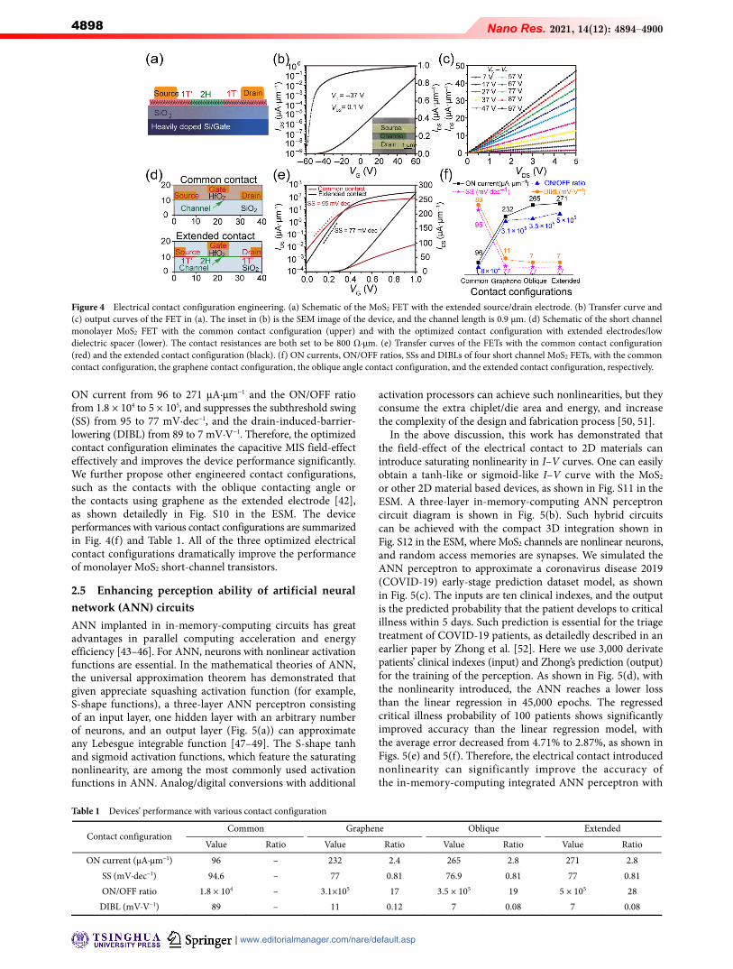
2.4 Engineering the electrical contact configuration
The comprehension of field-effect at the electrical contact to 2D materials leads to an interesting question of whether to eliminate it or use it, depending on different application scenarios. For 2D material-based transistors, the field-effect at electrical contact saturates the ON current and hinders the devices’ driving ability. The field-effect is critically dependent on the configuration. An elaborately designed electrical contact configuration should be able to eliminate the capacitive MIS field-effect effectively. As shown in Fig. 4(a) and Fig. S9 in the ESM, extended electrodes are realized by the butyl lithium induced 2H/1T' phase change transition, so that the sidewall of the metallic electrode is kept far away from the semiconducting channel. Such configuration eliminates the capacitive MIS field-effect, and subsequently, the current is not saturated, as shown in Figs. 4(b) and 4(c). Therefore, the efforts to improve the electrical contact to 2D materials should concentrate on not only the interface between the metallic electrode and 2D materials (to lower the contact resistance), but also the contact configuration (to eliminate the field-effect).
Using TCAD simulations, we further studied electrical monolayer MoS2 short-channel transistors (10 nm gate length, 20 nm source/drain distance) with various contact configurations. The contact resistance was uniformly set to 800 Ω·μm. Figure 4(d) shows two comparative transistors: The first transistor (upper) is with the common contact configuration, and the second transistor (lower) is with the optimized contact configuration, including the extended electrodes and the low dielectric spacer, to suppress the coupling through the capacitive MIS field-effect. The transfer curves of the two transistors are compared in Fig. 4(e). The red lines are from the transistor with the common contacts, and the black lines are from that with the extended electrode contacts. Compared to the common contact configuration, the extended electrode increases the
Figure 3 Capacitive MIS field-effect of the electrical contacts to graphene. Principle of the capacitive MIS field-effect for metal–graphene contacts, the depletion, accumulation, and inversion of the graphene channel: (a) n-region; (d) p-region. IDS–VDS curves of the graphene FET with the outer/inner electrode as the source/drain (left), and the inner/outer electrode as the source/drain (right): (b) n-region; (e) p-region. The differential conductance of the graphene FET with the outer/inner electrode as the source/drain (left), and the inner/outer electrode as the source/drain (right): (c) n-region (VG −VDirac = 52 V); (f) p-region (VG − VDirac = −68 V).
Nano Res. 2021, 14(12): 4894–4900
| www.editorialmanager.com/nare/default.asp
4898
ON current from 96 to 271 μA·μm−1 and the ON/OFF ratio from 1.8 × 10⁴ to 5 × 10⁵, and suppresses the subthreshold swing (SS) from 95 to 77 mV·dec−1, and the drain-induced-barrier- lowering (DIBL) from 89 to 7 mV·V−1. Therefore, the optimized contact configuration eliminates the capacitive MIS field-effect effectively and improves the device performance significantly. We further propose other engineered contact configurations, such as the contacts with the oblique contacting angle or the contacts using graphene as the extended electrode [42], as shown detailedly in Fig. S10 in the ESM. The device performances with various contact configurations are summarized in Fig. 4(f) and Table 1. All of the three optimized electrical contact configurations dramatically improve the performance of monolayer MoS2 short-channel transistors.
2.5 Enhancing perception ability of artificial neural
network (ANN) circuits
ANN implanted in in-memory-computing circuits has great advantages in parallel computing acceleration and energy efficiency [43–46]. For ANN, neurons with nonlinear activation functions are essential. In the mathematical theories of ANN, the universal approximation theorem has demonstrated that given appreciate squashing activation function (for example, S-shape functions), a three-layer ANN perceptron consisting of an input layer, one hidden layer with an arbitrary number of neurons, and an output layer (Fig. 5(a)) can approximate any Lebesgue integrable function [47–49]. The S-shape tanh and sigmoid activation functions, which feature the saturating nonlinearity, are among the most commonly used activation functions in ANN. Analog/digital conversions with additional
activation processors can achieve such nonlinearities, but they consume the extra chiplet/die area and energy, and increase the complexity of the design and fabrication process [50, 51].
In the above discussion, this work has demonstrated that the field-effect of the electrical contact to 2D materials can introduce saturating nonlinearity in I–V curves. One can easily obtain a tanh-like or sigmoid-like I–V curve with the MoS2 or other 2D material based devices, as shown in Fig. S11 in the ESM. A three-layer in-memory-computing ANN perceptron circuit diagram is shown in Fig. 5(b). Such hybrid circuits can be achieved with the compact 3D integration shown in Fig. S12 in the ESM, where MoS2 channels are nonlinear neurons, and random access memories are synapses. We simulated the ANN perceptron to approximate a coronavirus disease 2019 (COVID-19) early-stage prediction dataset model, as shown in Fig. 5(c). The inputs are ten clinical indexes, and the output is the predicted probability that the patient develops to critical illness within 5 days. Such prediction is essential for the triage treatment of COVID-19 patients, as detailedly described in an earlier paper by Zhong et al. [52]. Here we use 3,000 derivate patients’ clinical indexes (input) and Zhong’s prediction (output) for the training of the perception. As shown in Fig. 5(d), with the nonlinearity introduced, the ANN reaches a lower loss than the linear regression in 45,000 epochs. The regressed critical illness probability of 100 patients shows significantly improved accuracy than the linear regression model, with the average error decreased from 4.71% to 2.87%, as shown in Figs. 5(e) and 5(f). Therefore, the electrical contact introduced nonlinearity can significantly improve the accuracy of the in-memory-computing integrated ANN perceptron with
Figure 4 Electrical contact configuration engineering. (a) Schematic of the MoS2 FET with the extended source/drain electrode. (b) Transfer curve and (c) output curves of the FET in (a). The inset in (b) is the SEM image of the device, and the channel length is 0.9 μm. (d) Schematic of the short channelmonolayer MoS2 FET with the common contact configuration (upper) and with the optimized contact configuration with extended electrodes/lowdielectric spacer (lower). The contact resistances are both set to be 800 Ω·μm. (e) Transfer curves of the FETs with the common contact configuration (red) and the extended contact configuration (black). (f) ON currents, ON/OFF ratios, SSs and DIBLs of four short channel MoS2 FETs, with the common contact configuration, the graphene contact configuration, the oblique angle contact configuration, and the extended contact configuration, respectively.
Table 1 Devices’ performance with various contact configuration
Common Graphene Oblique Extended Contact configuration
Value Ratio Value Ratio Value Ratio Value Ratio ON current (μA·μm−1) 96 – 232 2.4 265 2.8 271 2.8
www.theNanoResearch.com∣www.Springer.com/journal/12274 | Nano Research
4899
compact device geometry compared to normal transistor devices working in the saturation region.
3 Conclusion This work proposes and demonstrates a field-effect at the electrical contacts to 2D materials, which has long been neglected in previous studies. The field-effect can deplete and accumulate the carriers, change the carrier densities and types, and introduce current saturation and nonlinearity. Based on such comprehension, on one hand, we call for attention to the optimization of the electrical contact configuration for 2D material transistors, which increases the current driving ability of devices. On the other hand, we demonstrate that the nonlinearity introduced by the field-effect at the electrical contact can enhance the perception ability of the hybrid ANN circuits. The principle in this work is general and applies to a wide range of 2D material devices. The full comprehension of the electrical contacts to 2D materials is fundamental to the simulation, design, and fabrication of 2D material-based electronic devices.
Acknowledgements We thank Prof. H.-S. Philip Wong from Stanford University and Analysis & Testing Center, Beijing Institute of Technology for the support of this work. We thank Prof. Zhiyong Zhang and Prof. Qing Chen from Peking University for useful discussion. Yao Guo thanks Dr. I-Ting Wang for the valuable suggestions. This work was supported the National Natural Science Foundation of China (No.11804024).
Electronic Supplementary Material: Supplementary material (results of the simulation and SEM) is available in the online version of this article at https://doi.org/10.1007/s12274-021- 3670-y.
References [1] Desai, S. B.; Madhvapathy, S. R.; Sachid, A. B.; Llinas, J. P.; Wang,
Q. X.; Ahn, G. H.; Pitner, G.; Kim, M. J.; Bokor, J.; Hu, C. M. et al. MoS2 transistors with 1-nanometer gate lengths. Science 2016, 354, 99–102.
[2] Huyghebaert, C.; Schram, T.; Smets, Q.; Agarwal, T. K.; Verreck, D.; Brems, S.; Phommahaxay, A.; Chiappe, D.; El Kazzi, S.; De La Rosa, C. L. et al. 2D materials: Roadmap to CMOS integration. In Proceedings of the 2018 IEEE International Electron Devices Meeting, San Francisco, 2018, pp 22.1.1–22.1.4.
[3] Akinwande, D.; Huyghebaert, C.; Wang, C. H.; Serna, M. I.; Goossens, S.; Li, L. J.; Wong, H. S. P.; Koppens, F. H. L. Graphene and two-dimensional materials for silicon technology. Nature 2019, 573, 507–518.
[4] Chen, M. L.; Sun, X. D.; Liu, H.; Wang, H. W.; Zhu, Q. B.; Wang, S. S.; Du, H. F.; Dong, B. J.; Zhang, J.; Sun, Y. et al. A FinFET with one atomic layer channel. Nat. Commun. 2020, 11, 1205.
[6] Li, L. K.; Yu, Y. J.; Ye, G. J.; Ge, Q. Q.; Ou, X. D.; Wu, H.; Feng, D. L.; Chen, X. H.; Zhang, Y. B. Black phosphorus field-effect transistors. Nat. Nanotechnol. 2014, 9, 372–377.
[7] Bandurin, D. A.; Tyurnina, A. V.; Yu, G. L.; Mishchenko, A.; Zólyomi, V.; Morozov, S. V.; Kumar, R. K.; Gorbachev, R. V.; Kudrynskyi, Z. R.; Pezzini, S. et al. High electron mobility, quantum hall effect and anomalous optical response in atomically thin InSe. Nat. Nanotechnol. 2017, 12, 223–227.
[8] Liu, T.; Liu, S.; Tu, K. H.; Schmidt, H.; Chu, L. Q.; Xiang, D.; Martin, J.; Eda, G.; Ross, C. A.; Garaj, S. Crested two-dimensional transistors. Nat. Nanotechnol. 2019, 14, 223–226.
[9] Liu, C. S.; Chen, H. W.; Wang, S. Y.; Liu, Q.; Jiang, Y. G.; Zhang, D. W.; Liu, M.; Zhou, P. Two-dimensional materials for next-generation computing technologies. Nat. Nanotechnol. 2020, 15, 545–557.
[10] Shi, Y. Y.; Liang, X. H.; Yuan, B.; Chen, V.; Li, H. T.; Hui, F.; Yu, Z. C. W.; Yuan, F.; Pop, E.; Wong, H. S. P. et al. Electronic synapses made of layered two-dimensional materials. Nat. Electron. 2018, 1, 458–465.
[11] Pan, C.; Wang, C. Y.; Liang, S. J.; Wang, Y.; Cao, T. J.; Wang, P. F.; Wang, C.; Wang, S.; Cheng, B.; Gao, A. Y. et al. Reconfigurable logic and neuromorphic circuits based on electrically tunable two-dimensional homojunctions. Nat. Electron. 2020, 3, 383–390.
[12] Wang, M.; Cai, S. H.; Pan, C.; Wang, C. Y.; Lian, X. J.; Zhuo, Y.; Xu, K.; Cao, T. J.; Pan, X. Q.; Wang, B. G. et al. Robust memristors based on layered two-dimensional materials. Nat. Electron. 2018, 1, 130–136.
[13] Hus, S. M.; Ge, R. J.; Chen, P. A.; Liang, L. B.; Donnelly, G. E.; Ko, W.; Huang, F. M.; Chiang, M. H.; Li, A. P.; Akinwande, D. Observation of single-defect memristor in an MoS2 atomic sheet. Nat. Nanotechnol. 2021, 16, 58–62.
[14] Chen, S. C.; Mahmoodi, M. R.; Shi, Y. Y.; Mahata, C.; Yuan, B.; Liang, X. H.; Wen, C.; Hui, F.; Akinwande, D.; Strukov, D. B. et al.
Figure 5 Enhancing perceptron ability in ANN circuits with nonlinearity. (a) Schematic of a three-layer ANN. (b) Circuit diagram of the ANN in-memory-computing. (c) Schematic of the COVID-19 early-stage prediction model. COPD: Chronic obstructive pulmonary disease. LD: Lactatedehydrogenase. NLR: Neutrophil/lymphocytes ratio. (d) Loss in the training process. The predicted probability (e) with and (f) without nonlinearity in the ANN circuits. The dotted reference lines are from Zhong et al.'s model described in their earlier paper [52].
Nano Res. 2021, 14(12): 4894–4900
| www.editorialmanager.com/nare/default.asp
4900
Wafer-scale integration of two-dimensional materials in high-density memristive crossbar arrays for artificial neural networks. Nat. Electron. 2020, 3, 638–645.
[15] Kong, L. G.; Chen, Y.; Liu, Y. Recent progresses of NMOS and CMOS logic functions based on two-dimensional semiconductors. Nano Res. 2021, 14, 1768–1783.
[16] Zeng, S. F.; Tang, Z. W.; Liu, C. S.; Zhou, P. Electronics based on two-dimensional materials: Status and outlook. Nano Res. 2021, 14, 1752–1767.
[17] Pudasaini, P. R.; Oyedele, A.; Zhang, C.; Stanford, M. G.; Cross, N.; Wong, A. T.; Hoffman, A. N.; Xiao, K.; Duscher, G.; Mandrus, D. G. et al. High-performance multilayer WSe2 field-effect transistors with carrier type control. Nano Res. 2018, 11, 722–730.
[18] Allain, A.; Kang, J. H.; Banerjee, K.; Kis, A. Electrical contacts to two-dimensional semiconductors. Nat. Mater. 2015, 14, 1195–1205.
[19] Liu, H.; Si, M. W.; Deng, Y. X.; Neal, A. T.; Du, Y. C.; Najmaei, S.; Ajayan, P. M.; Lou, J.; Ye, P. D. Switching mechanism in single-layer molybdenum disulfide transistors: an insight into current flow across Schottky barriers. ACS Nano 2014, 8, 1031–1038.
[20] Guo, Y.; Han, Y. X.; Li, J. P.; Xiang, A.; Wei, X. L.; Gao, S.; Chen, Q. Study on the resistance distribution at the contact between molybdenum disulfide and metals. ACS Nano 2014, 8, 7771–7779.
[21] Li, J.; Yang, X. D.; Liu, Y.; Huang, B. L.; Wu, R. X.; Zhang, Z. W.; Zhao, B.; Ma, H. F.; Dang, W. Q.; Wei, Z. et al. General synthesis of two-dimensional van der Waals heterostructure arrays. Nature 2020, 579, 368–374.
[22] Xia, F. N.; Perebeinos, V.; Lin, Y. M.; Wu, Y. Q.; Avouris, P. The origins and limits of metal–graphene junction resistance. Nat. Nanotechnol. 2011, 6, 179–184.
[23] Das, S.; Chen, H. Y.; Penumatcha, A. V.; Appenzeller, J. High performance multilayer MoS2 transistors with Scandium contacts. Nano Lett. 2013, 13, 100–105.
[24] Zheng, X. R.; Calò, A.; Albisetti, E.; Liu, X. Y.; Alharbi, A. S. M.; Arefe, G.; Liu, X. C.; Spieser, M.; Yoo, W. J.; Taniguchi, T. et al. Patterning metal contacts on monolayer MoS2 with vanishing Schottky barriers using thermal nanolithography. Nat. Electron. 2019, 2, 17–25.
[25] English, C. D.; Shine, G.; Dorgan, V. E.; Saraswat, K. C.; Pop, E. Improved contacts to MoS2 transistors by ultra-high vacuum metal deposition. Nano Lett. 2016, 16, 3824–3830.
[26] Rai, A.; Valsaraj, A.; Movva, H. C. P.; Roy, A.; Ghosh, R.; Sonde, S.; Kang, S.; Chang, J.; Trivedi, T.; Dey, R. et al. Air stable doping and intrinsic mobility enhancement in monolayer molybdenum disulfide by amorphous Titanium suboxide encapsulation. Nano Lett. 2015, 15, 4329–4336.
[27] McClellan, C. J.; Yalon, E.; Smithe, K. K. H.; Suryavanshi, S. V.; Pop, E.; High current density in monolayer MoS2 doped by AlOx. ACS Nano 2021, 15, 1587–1596
[28] Yang, L. M.; Majumdar, K.; Liu, H.; Du, Y. C.; Wu, H.; Hatzistergos, M.; Hung, P. Y.; Tieckelmann, R.; Tsai, W.; Hobbs, C. et al. Chloride molecular doping technique on 2D materials: WS2 and MoS2. Nano Lett. 2014, 14, 6275–6280.
[29] Dong, L.; Wang, X. W.; Zhang, J. Y.; Li, X. F.; Lou, X. B.; Conrad, N.; Wu, H.; Gordon, R. G.; Ye, P. D. III–V CMOS devices and circuits with high-quality atomic-layer-epitaxial La2O3/GaAs interface. In Proceedings of 2014 Symposium on VLSI Technology (VLSI-Technology): Digest of Technical Papers, Honolulu, 2014, pp 1–2.
[30] Kappera, R.; Voiry, D.; Yalcin, S. E.; Branch, B.; Gupta, G.; Mohite, A. D.; Chhowalla, M. Phase-engineered low-resistance contacts for ultrathin MoS2 transistors. Nat. Mater. 2014, 13, 1128–1134.
[31] Song, S.; Sim, Y.; Kim, S. Y.; Kim, J. H.; Oh, I.; Na, W.; Lee, D. H.; Wang, J.; Yan, S. L.; Liu, Y. N. et al. Wafer-scale production of patterned transition metal ditelluride layers for two-dimensional metal–semiconductor contacts at the Schottky–Mott limit. Nat. Electron. 2020, 3, 207–215.
[32] Wang, Y.; Kim, J. C.; Wu, R. J.; Martinez, J.; Song, X. J.; Yang, J.; Zhao, F.; Mkhoyan, A.; Jeong, H. Y.; Chhowalla, M. Van der Waals
contacts between three-dimensional metals and two-dimensional semiconductors. Nature 2019, 568, 70–74.
[33] Liu, Y.; Guo, J.; Zhu, E. B.; Liao, L.; Lee, S. J.; Ding, M. N.; Shakir, I.; Gambin, V.; Huang, Y.; Duan, X. F. Approaching the Schottky-Mott limit in van der Waals metal-semiconductor junctions. Nature 2018, 557, 696–700.
[34] Li, X. F.; Yang, L. M.; Si, M. W.; Li, S. C.; Huang, M. Q.; Ye, P. D.; Wu, Y. Q. Performance potential and limit of MoS2 transistors. Adv. Mater. 2015, 27, 1547–1552.
[35] Fiori, G.; Szafranek, B. N.; Iannaccone, G.; Neumaier, D. Velocity saturation in few-layer MoS2 transistor. Appl. Phys. Lett. 2013, 103, 233509.
[36] Liu, W.; Kang, J. H.; Sarkar, D.; Khatami, Y.; Jena, D.; Banerjee, K. Role of metal contacts in designing high-performance monolayer n-type WSe2 field effect transistors. Nano Lett. 2013, 13, 1983–1990.
[37] Smithe, K. K. H.; English, C. D.; Suryavanshi, S. V.; Pop, E. High-field transport and velocity saturation in synthetic monolayer MoS2. Nano Lett. 2018, 18, 4516–4522.
[38] Du, H.; Kim, T.; Shin, S.; Kim, D.; Kim, H.; Sung, J. H.; Lee, M. J.; Seo, D. H.; Lee, S. W.; Jo, M. H. et al. Schottky barrier contrasts in single and bi-layer graphene contacts for MoS2 field-effect transistors. Appl. Phys. Lett. 2015, 107, 233106.
[39] Zhang, Z.; Yao, K.; Liu, Y.; Jin, C.; Liang, X.; Chen, Q.; Peng, L. M. Quantitative analysis of current–voltage characteristics of semiconducting nanowires: Decoupling of contact effects. Adv. Funct. Mater. 2007, 17, 2478–2489.
[40] Gupta, S.; Rortais, F.; Ohshima, R.; Ando, Y.; Endo, T.; Miyata, Y.; Shiraishi, M. Monolayer MoS2 field effect transistor with low schottky barrier height with ferromagnetic metal contacts. Sci. Rep. 2019, 9, 17032.
[41] Cheng, Q.; Ahmad, W.; Liu, G. H.; Wang, K. Y. Structural evolution of amorphous thin films of titanium dioxide. In Proceedings of the 2011 11th IEEE International Conference on Nanotechnology, Portland, 2011, pp 1598–1601.
[42] Du, Y. C.; Yang, L. M.; Zhang, J. Y.; Liu, H.; Majumdar, K.; Kirsch, P. D.; Ye, P. D. MoS2 field-effect transistors with graphene/metal heterocontacts. IEEE Electron Device Lett. 2014, 35, 599–601.
[43] Sebastian, A.; Gallo, M. L.; Khaddam-Aljameh, R.; Eleftheriou, E. Memory devices and applications for in-memory computing. Nat. Nanotechnol. 2020, 15, 529–544.
[44] Ielmini, D.; Pedretti, G. Device and circuit architectures for in-memory computing. Adv. Intell. Syst. 2020, 2, 2000040.
[45] Ielmini, D.; Wong, H. S. P. In-memory computing with resistive switching devices. Nat. Electron. 2018, 1, 333–343.
[46] Lee, S. H.; Zhu, X. J.; Lu, W. D. Nanoscale resistive switching devices for memory and computing applications. Nano Res. 2020, 13, 1228–1243.
[47] Hornik, K. Approximation capabilities of multilayer feedforward networks. Neural Netw. 1991, 4, 251–257.
[48] Leshno, M.; Lin, V. Y.; Pinkus, A.; Schocken, S. Multilayer feedforward networks with a nonpolynomial activation function can approximate any function. Neural Netw. 1993, 6, 861–867.
[49] Cybenko, G. Approximation by superpositions of a sigmoidal function. Math. Control Signals Syst. 1989, 2, 303–314.
[50] Pei, J.; Deng, L.; Song, S.; Zhao, M. G.; Zhang, Y. H.; Wu, S.; Wang, G. R.; Zou, Z.; Wu, Z. Z.; He, W. et al. Towards artificial general intelligence with hybrid Tianjic chip architecture. Nature 2019, 572, 106–111.
[51] Yan, B. N.; Yang, Q.; Chen, W. H.; Chang, K. T.; Su, J. W.; Hsu, C. H.; Li, S. H.; Lee, H. Y.; Sheu, S. S.; Ho, M. S. et al. RRAM-based spiking nonvolatile computing-in-memory processing engine with precision-configurable in situ nonlinear activation. In Proceedings of the 2019 Symposium on VLSI Technology, Kyoto, Japan, 2019, pp T86–T87.
[52] Liang, W. H.; Yao, J. H.; Chen, A. L.; Lv, Q. Q.; Zanin, M.; Liu, J.; Wong, S.; Li, Y. M.; Lu, J. T.; Liang, H. R. et al. Early triage of critically ill COVID-19 patients using deep learning. Nat. Commun. 2020, 11, 3543.


![Braunovic - Electrical Contacts - Fundamentals, Applications and Technology [Missing Index] (CRC, 2007)](https://static.documents.pub/doc/80x56/557212d1497959fc0b910194/braunovic-electrical-contacts-fundamentals-applications-and-technology.jpg)


