Page 1
FIELD ORIENTED CONTROL OF A PERMANENT MAGNET
SYNCHRONOUS MOTOR USING SPACE VECTOR MODULATED DIRECT AC-AC MATRIX CONVERTER
A THESIS SUBMITTED TO
THE GRADUATE SCHOOL OF NATURAL AND APPLIED SCIENCES
OF
MIDDLE EAST TECHNICAL UNIVERSITY
BY
DOĞAN YILDIRIM
IN PARTIAL FULLFILLMENT OF THE REQUIREMENTS
FOR
THE DEGREE OF MASTER OF SCIENCE
IN
ELECTRICAL AND ELECTRONICS ENGINEERING
MAY 2012
Page 2
Approval of the thesis:
FIELD ORIENTED CONTROL OF A PERMANENT MAGNET
SYNCHRONOUS MOTOR USING SPACE VECTOR MODULATED
DIRECT AC-AC MATRIX CONVERTER
submitted by DOĞAN YILDIRIM in partial fulfillment of the requirements for the
degree of Master of Science in Electrical and Electronics Engineering
Department, Middle East Technical University by,
Prof. Dr. Canan ÖZGEN
Dean, Graduate School of Natural and Applied Sciences
Prof. Dr. Ġsmet ERKMEN
Head of Department, Electrical and Electronics Engineering
Prof. Dr. Aydın ERSAK
Supervisor, Electrical and Electronics Engineering Dept., METU
Examining Committee Members:
Prof. Dr. Muammer ERMĠġ
Electrical and Electronics Engineering Dept., METU
Prof. Dr. Aydın ERSAK
Electrical and Electronics Engineering Dept., METU
Prof. Dr. IĢık ÇADIRCI
Electrical and Electronics Engineering Dept., HU
Dr. Faruk BĠLGĠN
Space Technologies Research Institute, TÜBĠTAK
Dr. Bilge MUTLUER
Space Technologies Research Institute, TÜBĠTAK
Date: 10.05.2012
Page 3
iii
I hereby declare that all information in this document has been obtained and
presented in accordance with academic rules and ethical conduct. I also
declare that, as required by these rules and conduct, I have fully cited and
referenced all material and results that are not original to this work.
Name, Last name : Doğan YILDIRIM
Signature :
Page 4
iv
ABSTRACT
FIELD ORIENTED CONTROL OF A PERMANENT MAGNET
SYNCHRONOUS MOTOR USING SPACE VECTOR MODULATED
DIRECT AC-AC MATRIX CONVERTER
Yıldırım, Doğan
M. Sc., Department of Electrical and Electronics Engineering
Supervisor: Prof. Dr. Aydın Ersak
May 2012, 167 pages
The study designs and constructs a three-phase to three-phase direct AC–AC matrix
converter based surface mounted permanent magnet synchronous motor (PMSM) drive
system. First, the matrix converter topologies are analyzed and the state-space equations
describing the system have been derived in terms of the input and output variables. After
that, matrix converter commutation and modulation methods are investigated. A four-step
commutation technique based on output current direction provides safe commutation
between the matrix converter switches. Then, the matrix converter is simulated for both the
open-loop and the closed-loop control. For the closed-loop control, a current regulator (PI
controller) controls the output currents and their phase angles. Advanced pulse width
modulation and control techniques, such as space vector pulse width modulation and field
oriented control, have been used for the closed-loop control of the system. Next, a model of
diode-rectified two-level voltage source inverter is developed for simulations. A
comparative study of indirect space vector modulated direct matrix converter and space
vector modulated diode-rectified two-level voltage source inverter is given in terms of
input/output waveforms to verify that the matrix converter fulfills the two-level voltage
source inverter operation. Following the verification of matrix converter operation
Page 5
v
comparing with the diode-rectified two-level voltage source inverter, the simulation model
of permanent magnet motor drive system is implemented. Also, a direct matrix converter
prototype is constructed for experimental verifications of the results. As a first step in
experimental works, filter types are investigated and a three-phase input filter is constructed
to reduce the harmonic pollution. Then, direct matrix converter power circuitry and gate-
driver circuitry are designed and constructed. To control the matrix switches, the control
algorithm is implemented using a DSP and a FPGA. This digital control system measures
the output currents and the input voltages with the aid of sensors and controls the matrix
converter switches to produce the required PWM pattern to synthesize the reference input
current and output voltage vectors, as well. Finally, the simulation results are tested and
supported by laboratory experiments involving both an R-L load and a permanent magnet
synchronous motor load. During the tests, the line-to-line supply voltage is set to 26 V peak
value and a 400 V/3.5 kW surface mounted permanent magnet motor is used.
Keywords: Direct matrix converter, bi-directional switch, space vector PWM, field oriented
control, SMPMS motor, three-phase diode rectifier, two-level inverter
Page 6
vi
ÖZ
UZAY VEKTÖR MODULASYONLU DĠREK AC-AC MATRĠS ÇEVĠRĠCĠ
KULLANARAK KALICI MIKNATISLI SENKRON MOTORUN ALAN
YÖNLENDĠRMELĠ DENETĠMĠ
Yıldırım, Doğan
Yüksek Lisans, Elektrik Elektronik Mühendisliği Bölümü
Tez Yöneticisi: Prof. Dr. Aydın Ersak
Mayıs 2012, 167 sayfa
Bu çalıĢmada üç faz giriĢ ve üç faz çıkıĢlı matris çevirici topolojisine dayalı yüzey monte
kalıcı mıknatıslı eĢzamanlı motor sürücü sistemi tasarlanmakta ve inĢa edilmektedir. Ġlk
olarak, matris çevirici topolojileri analiz edilmektedir ve giriĢ - çıkıĢ değiĢkenleri cinsinden
sistemi tanımlayacak durum uzayı denklemleri çıkarılmaktadır. Daha sonra matris çevirici
komutasyon ve modülasyon metotları incelenmektedir. ÇıkıĢ akımının yönüne dayalı dört
basamaklı komutasyon tekniği ile matris çeviricinin güvenilir komutasyonu yapılmaktadır.
Sonra, matris çevirici kontrolü için açık ve kapalı döngü benzetim modelleri
oluĢturulmaktadır. ÇıkıĢ akımları ve faz açıları kapalı döngü kotrolü, PI kontrolcüsü
kullanılarak gerçeklenmektedir. Uzay vektör darbe geniĢlik modulasyonu ve alan
yönlendirmeli kotrol teknikleri gibi geliĢmiĢ modulasyon ve kontrol teknikleri
kullanılmaktadır. Daha sonra, diyot doğrultmalı iki seviyeli voltaj kaynaklı evirici modeli
geliĢtirilmektedir. Matris çeviricinin bu evirici yapısının fonksiyonlarını yerine
getirebildiğini doğrulamak amacıyla bu iki topolojinin giriĢ ve çıkıĢ dalga formları birbirleri
ile karĢılaĢtırılmaktadır. Matris çeviricinin bu iki seviyeli yapının fonksiyonlarını yerine
getirebildiği doğrulandıktan sonra kalıcı mıknatıslı motor sürücü sistemi benzetim modeli
gerçeklenmektedir. Bununla birlikte, deneysel doğrulamalar için matris çevirici devresi inĢa
Page 7
vii
edilmektedir. Deneysel çalıĢmalarda ilk olarak, filtre türleri incelenmekte ve harmonik
kirliliği önlemek amaçlı üç faz giriĢ filtresi inĢa edilmektedir. Sonra, direk matris çevirici
güç devresi ve “gate” sürücü devresi tasarlanmakta ve üretilmektedir. Matris çevirici
üzerinde bulunan anahtarları kontol etmek için FPGA ve DSP kullanılmaktadır. Dijital
kontrol sistemi ile çıkıĢ akımları ve giriĢ gerilim bilgileri okunmakta, hesaplanan akım ve
voltaj vektörlerinin sentezlenmesi için gerekli anahtarlama iĢaretleri oluĢturulmaktadır. Son
olarak, simülasyon sonuçları pasif R-L yük ve motor yükü kullanılarak denysel çalıĢma
sonuçlarıyla test edilmekte ve desteklenmektedir. Testler boyunca, fazdan faza olan
besleme voltaj değeri 26 V tepe gerilim değerine ayarlanmakta ve 400 V/3.5 kW’lık yüzey
monte kalıcı mıknatıslı motor deneysel çalıĢmalarda kullanılmaktadır.
Anahtar Kelimeler: Direk matris çevirici, çift yönlü anahtar, uzay vektörü darbe geniĢliği
modulasyonu, alan yönlendirmeli kontrol, yüzey monte kalıcı mıknatıslı senkron motor, üç
faz diyot doğrultucu, iki seviyeli evirici
Page 9
ix
ACKNOWLEDGEMENTS
I express my gratitude to my supervisor Prof. Dr. Aydın ERSAK for his guidance, support,
criticism, encouragement and contributions throughout my graduate education.
I would also like to thank my colleagues and managers at ASELSAN Inc. for their
understanding, help and support. I am also grateful to ASELSAN Inc. for the financial
support.
Finally, I would like to thank my parents and wife, who have always been enriching my life
with their continuous support and love.
Page 10
x
TABLE OF CONTENTS
ABSTRACT ...................................................................................................................................... IV
ÖZ ...................................................................................................................................................... VI
ACKNOWLEDGEMENTS ............................................................................................................. IX
TABLE OF CONTENTS .................................................................................................................. X
LIST OF FIGURES ...................................................................................................................... XIII
LIST OF TABLES ..................................................................................................................... XVIII
LIST OF ABBREVIATIONS ....................................................................................................... XIX
NOMENCLATURE ........................................................................................................................XX
CHAPTERS
1. INTRODUCTION .......................................................................................................................... 1
1.1 AC/AC POWER CONVERSION .............................................................................................. 1
1.1.1 Overview of Indirect (DC-link) Two-Level Voltage Source Converters........................... 3
1.1.2 History of Direct AC/AC Converters ................................................................................ 5
1.1.3 Concept of Matrix Converter ............................................................................................. 7
1.2 SCOPE OF THESIS AND STRUCTURE OF CHAPTERS ...................................................... 8
2. THE PERMANENT MAGNET SYNCHRONOUS MACHINE (PMSM) DRIVE SYSTEM
USING DIRECT MATRIX CONVERTER ................................................................................... 10
2.1 STRUCTURE OF PERMANENT MAGNET MACHINE DRIVE SYSTEM......................... 10
2.2 FUNDAMENTALS OF MATRIX CONVERTER .................................................................. 12
2.3 INPUT-OUTPUT CHARACTERISTICS OF MATRIX CONVERTER................................. 12
2.3.1 Output Voltages and Currents.......................................................................................... 12
2.3.2 Input Voltages and Currents ............................................................................................ 14
2.4 STRUCTURAL ISSUES OF MATRIX CONVERTER .......................................................... 16
2.4.1 Direct Matrix Converter................................................................................................... 17
2.4.2 Indirect Matrix Converter ................................................................................................ 18
2.4.3 Bi-directional Switches .................................................................................................... 20
Page 11
xi
2.4.4 Commutation Problem ..................................................................................................... 23
2.4.5 Safe Operation ................................................................................................................. 23
2.4.6 Switch Commutation ....................................................................................................... 26
3. PERMANENT MAGNET SYNCHRONOUS MACHINES..................................................... 42
3.1 STEADY-STATE MODELING OF SMPM SYNCHRONOUS MACHINE .......................... 43
3.2 DYNAMIC MODELING OF THE SMPM SYNCHRONOUS MACHINE ............................ 46
4. OPERATIONAL ISSUES OF MATRIX CONVERTER ......................................................... 50
4.1 STATE-SPACE MODEL OF MATRIX CONVERTER ......................................................... 50
4.2 VOLTAGE AND CURRENT WAVEFORMS GENERATION IN MATRIX CONVERTERS
....................................................................................................................................................... 53
4.2.1 Matrix Converter Modulation Methods of Alesina and Venturini ................................... 55
4.2.2 Space Vector .................................................................................................................... 58
4.2.3 Application of Space Vector PWM Methods in the Matrix Converter ............................ 60
4.2.4 Application of the Indirect Space Vector PWM for Direct Matrix Converter ................. 76
5. SYSTEM MODELING AND SIMULATIONS ......................................................................... 83
5.1 MODELING OF DIRECT MATRIX CONVERTER .............................................................. 83
5.1.1 Input Filter Design ........................................................................................................... 84
5.1.2 Construction of Bi-directional Power Switch Structures ................................................. 89
5.1.3 Steps for the Simulation of Indirect Space Vector PWM for the Direct Matrix Converter
.................................................................................................................................................. 89
5.2 SIMULATIONS ON DIRECT MATRIX CONVERTER REGARDING TO OUTPUT
CHARACTERISTICS ................................................................................................................... 90
5.2.1 Simulations of Open-Loop System with Balanced R-L Load.......................................... 91
5.2.2 Closed-Loop Simulations with Balanced Three-Phase R-L Load ................................. 105
5.3 SIMULATIONS ON DIRECT MATRIX CONVERTER REGARDING TO INPUT
CHARACTERISTICS ................................................................................................................. 111
5.4 SIMULATIONS ON DIODE-RECTIFIED TWO-LEVEL VOLTAGE SOURCE INVERTER
STRUCTURE .............................................................................................................................. 113
5.5 COMPARISON OF THE DIODE-RECTIFIED TWO-LEVEL VOLTAGE SOURCE
INVERTER AND DIRECT MATRIX CONVERTER ................................................................ 116
5.6 MODELING OF THE DIRECT MATRIX CONVERTER INTEGRATED DRIVE SYSTEM
AND SIMULATIONS................................................................................................................. 118
5.6.1 Field Oriented Control of a Permanent Magnet Synchronous Motor ............................ 118
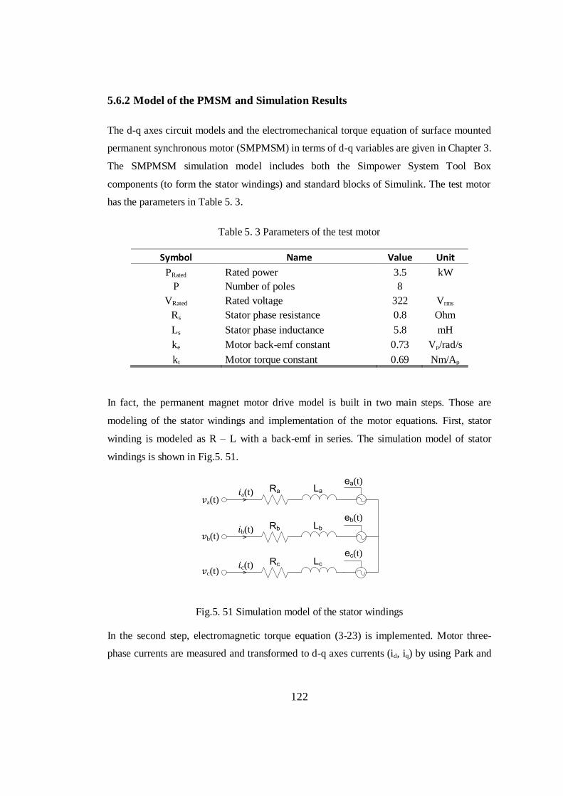
5.6.2 Model of the PMSM and Simulation Results ................................................................ 122
Page 12
xii
6. EXPERIMENTAL WORK ....................................................................................................... 129
6.1 HARDWARE IMPLEMENTATION .................................................................................... 129
6.2 MEASUREMENT EQUIPMENTS ....................................................................................... 134
6.3 EXPERIMENTAL RESULTS ............................................................................................... 135
6.3.1 Open-Loop Output Characteristics with Balanced R-L Load ........................................ 135
6.3.2 Closed-Loop Output Characteristics with Balanced R-L Load ..................................... 141
6.3.3 Unity Power Factor Control ........................................................................................... 148
6.3.4 Experiments with Surface Mounted Permanent Magnet Machine Load ....................... 151
7. CONCLUSIONS AND FUTURE WORKS ............................................................................. 155
REFERENCES ............................................................................................................................... 159
APPENDIX ..................................................................................................................................... 164
A. PARK AND CLARKE TRANSFORMATIONS .................................................................... 164
A.1. CLARKE TRANSFORMATION ...................................................................................... 164
A.2. PARK TRANSFORMATION ........................................................................................... 166
Page 13
xiii
LIST OF FIGURES
FIGURES
Fig.1. 1 Classifications of converters low-to-high power drives ......................................................... 2
Fig.1. 2 Three-phase two-level voltage source inverter circuit topology ............................................. 2
Fig.1. 3 Diode rectifier stage ................................................................................................................ 3
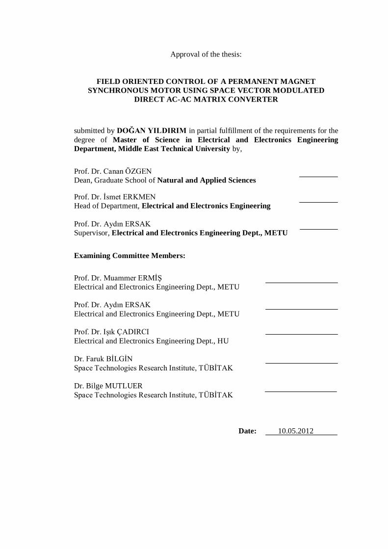
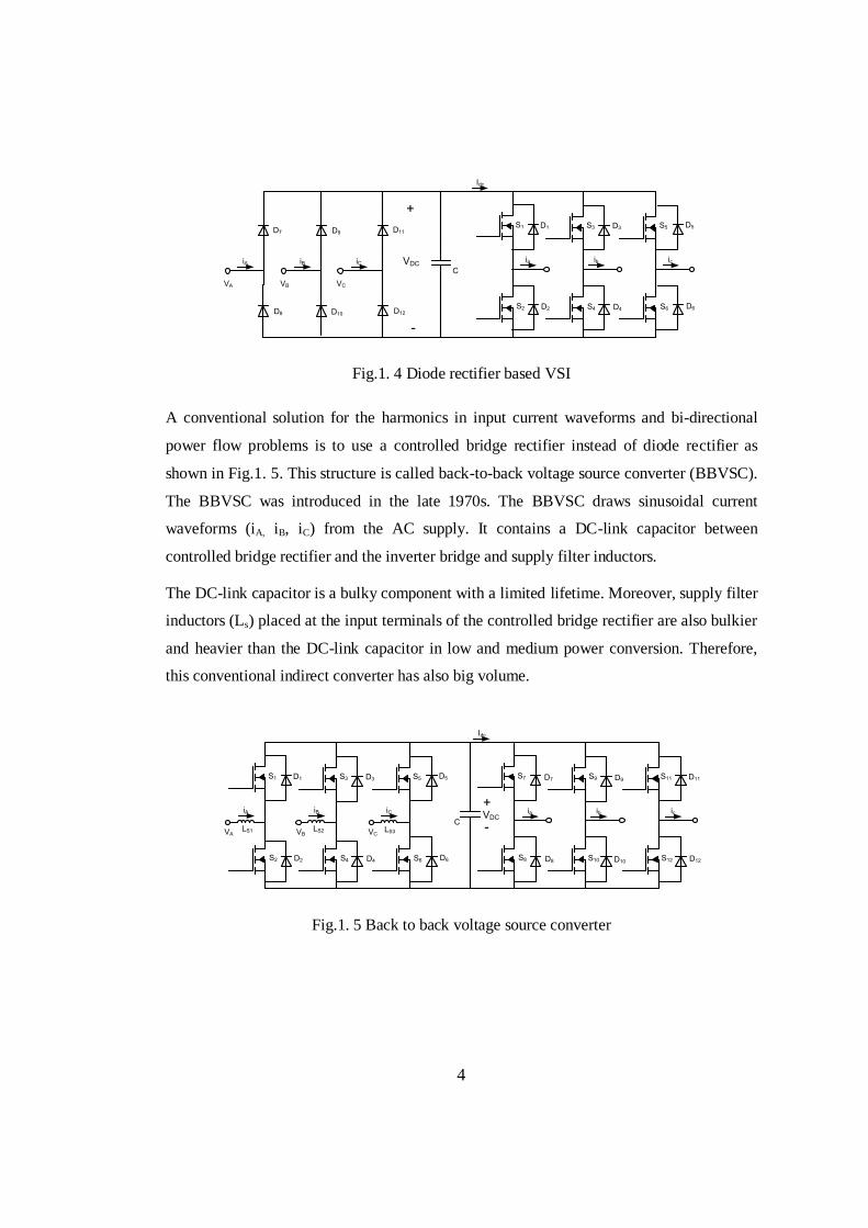
Fig.1. 4 Diode rectifier based VSI ........................................................................................................ 4
Fig.1. 5 Back to back voltage source converter .................................................................................... 4
Fig.1. 6 Phase-controlled thyristor-based three-phase to three-phase cycloconverter .......................... 5
Fig.1. 7 Basic direct matrix converter circuit ....................................................................................... 6
Fig.2. 1 PMSM drive basic architecture ............................................................................................. 11
Fig.2. 2 Block diagram of PMSM drive system ................................................................................. 11
Fig.2. 3 Structure of matrix converter system .................................................................................... 13
Fig.2. 4 Line-to-line output voltage waveform generated by direct matrix converter ........................ 13
Fig.2. 5 Three-phase output currents of a direct matrix converter ..................................................... 14
Fig.2. 6 Three-phase input voltages of direct matrix converter .......................................................... 14
Fig.2. 7 Unfiltered input phase “A” current ....................................................................................... 15
Fig.2. 8 Harmonic spectrum of unfiltered input phase A current (fs = 10 kHz) ................................. 15
Fig.2. 9 Filtered input phase A current ............................................................................................... 16
Fig.2. 10 Harmonic spectrum of filtered input phase A current (fs = 10 kHz) ................................... 16
Fig.2. 11 Structure of direct matrix converter .................................................................................... 17
Fig.2. 12 Structure of three-phase to four-phase direct matrix converter ........................................... 18
Fig.2. 13 Indirect three-phase to three-phase matrix converter .......................................................... 19
Fig.2. 14 An equivalent switching combination of direct and indirect matrix converter ................... 19
Fig.2. 15 Diode bridge structure ......................................................................................................... 20
Fig.2. 16 Common source AC switch configuration .......................................................................... 21
Fig.2. 17 Common drain AC switch configuration ............................................................................ 22
Fig.2. 18 Anti-parallel series diode-MOSFET configuration ............................................................. 23
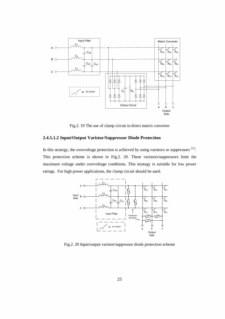
Fig.2. 19 The use of clamp circuit in direct matrix converter ............................................................ 25
Fig.2. 20 Input/output varistor/suppressor diode protection scheme .................................................. 25
Fig.2. 21 Line to line short circuit condition ...................................................................................... 27
Fig.2. 22 Output current interrupt ...................................................................................................... 27
Fig.2. 23 One output phase structure of direct matrix converter ........................................................ 29
Page 14
xiv
Fig.2. 24 One output phase structure .................................................................................................. 30
Fig.2. 25 Freewheeling current path in Leg2 ..................................................................................... 31
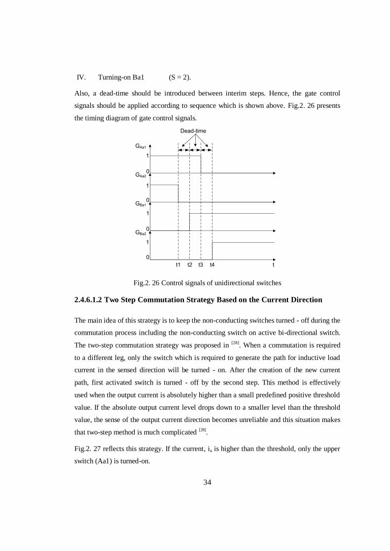
Fig.2. 26 Control signals of unidirectional switches .......................................................................... 34
Fig.2. 27 Inductive current path in two step commutation ................................................................. 35
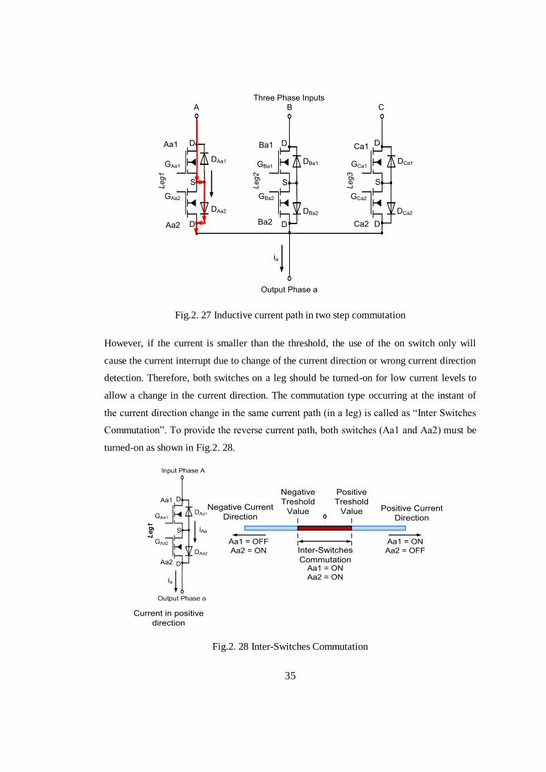
Fig.2. 28 Inter-Switches Commutation .............................................................................................. 35
Fig.2. 29 Allowed current directions ( > ) ................................................................................ 37
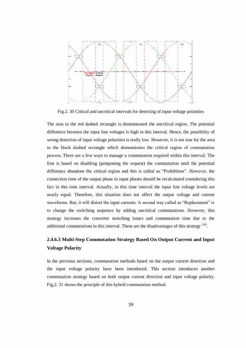
Fig.2. 30 Critical and uncritical intervals for detecting of input voltage polarities ............................ 39
Fig.2. 31 Critical and uncritical intervals for output current direction and input voltage polarity based
commutations............................................................................................................................ 40
Fig.3. 1 Permanent magnet rotor construction using surface mounted magnets ................................ 42
Fig.3. 2 Permanent magnet rotor construction using embedded magnets .......................................... 43
Fig.3. 3 Per-phase equivalent circuit of non-salient surface mounted permanent magnet synchronous
machine..................................................................................................................................... 44
Fig.3. 4 Phasor diagram of the non-salient SMPM machine .............................................................. 45
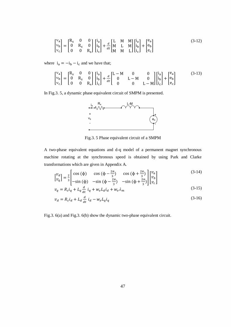
Fig.3. 5 Phase equivalent circuit of a SMPM ..................................................................................... 47
Fig.3. 6 Two-phase (d, q) equivalent model of SMPM synchronous machine .................................. 48
Fig.4. 1 Simplified three-phase to three-phase matrix converter........................................................ 51
Fig.4. 2 A possible switching pattern ................................................................................................. 56
Fig.4. 3 Three variables of balanced three-phase system ( , , ) .............................................. 59
Fig.4. 4 Space vector and its components ..................................................................................... 59
Fig.4. 5 Switching constraints (a) possible short circuit states at input terminal (b) open circuit state
at output terminals .................................................................................................................... 62
Fig.4. 6 (a) Output phase voltage vector (b) input line current vector hexagons................................ 64
Fig.4. 7 Indirect matrix converter circuit............................................................................................ 66
Fig.4. 8 Active current vectors, related sectors, and the reference phase current vector in complex
plane ......................................................................................................................................... 69
Fig.4. 9 Relationships between the input line current waveforms and the sectors in time domain .... 69
Fig.4. 10 Reference phase current vector construction....................................................................... 70
Fig.4. 11 Active output voltage space vectors, related sectors, and the reference output phase voltage
vector, in complex plane ..................................................................................................... 73
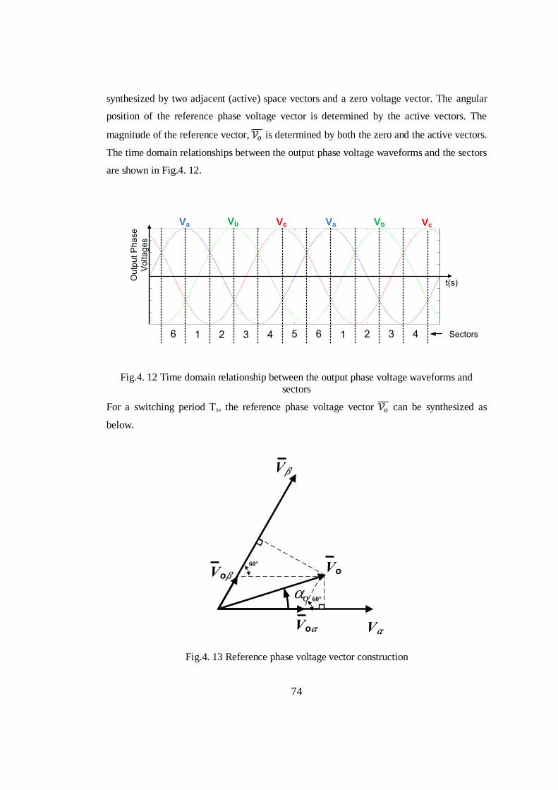
Fig.4. 12 Time domain relationship between the output phase voltage waveforms and sectors ........ 74
Fig.4. 13 Reference phase voltage vector construction ...................................................................... 74
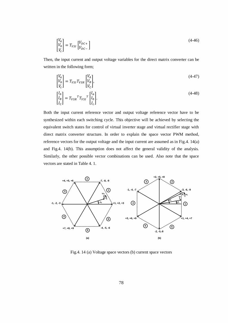
Fig.4. 14 (a) Voltage space vectors (b) current space vectors ............................................................ 78
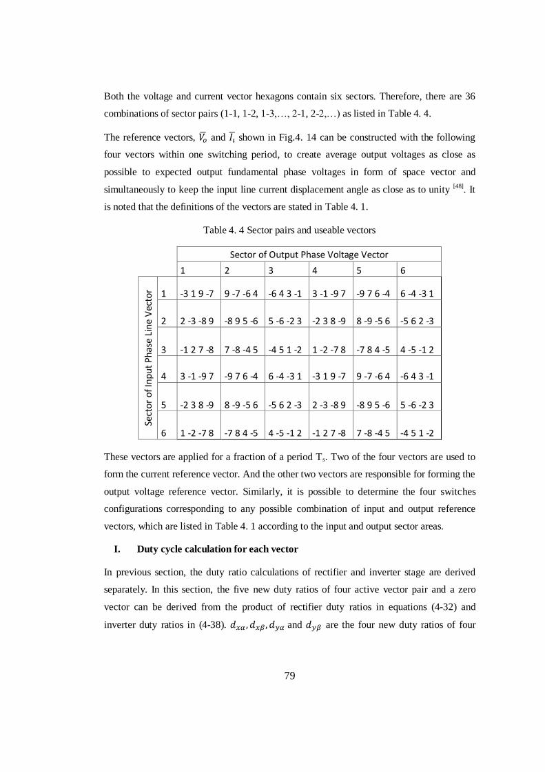
Fig.4. 15 Nine switching pulses for a carrier frequency of 10 kHz with single-sided switching pattern
.................................................................................................................................................. 81
Page 15
xv
Fig.4. 16 Nine switching pulses for a carrier frequency of 10 kHz with double-sided switching
pattern ....................................................................................................................................... 82
Fig.5. 1 Input filter configurations used for matrix converter input filters ......................................... 85
Fig.5. 2 Laplace transform of per-phase equivalent circuit ................................................................ 86
Fig.5. 3 Magnitude and phase plot of the LC filter with Rf = 94 Ohm ............................................... 87
Fig.5. 4 Magnitude and phase plot of the LC filter without damping resistor .................................... 87
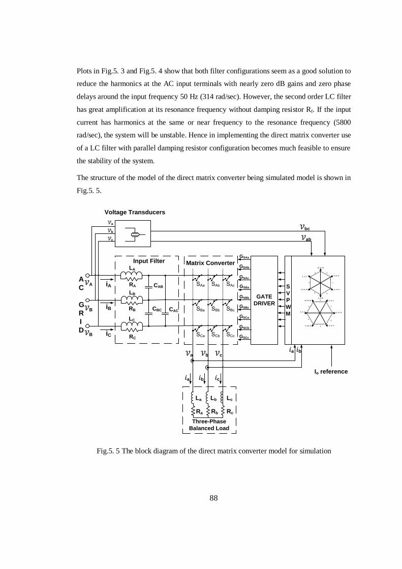
Fig.5. 5 The block diagram of the direct matrix converter model for simulation............................... 88
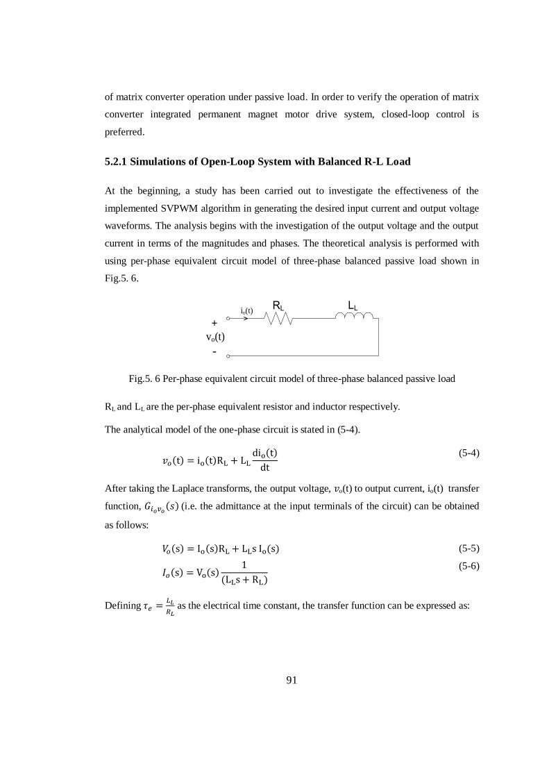
Fig.5. 6 Per-phase equivalent circuit model of three-phase balanced passive load ............................ 91
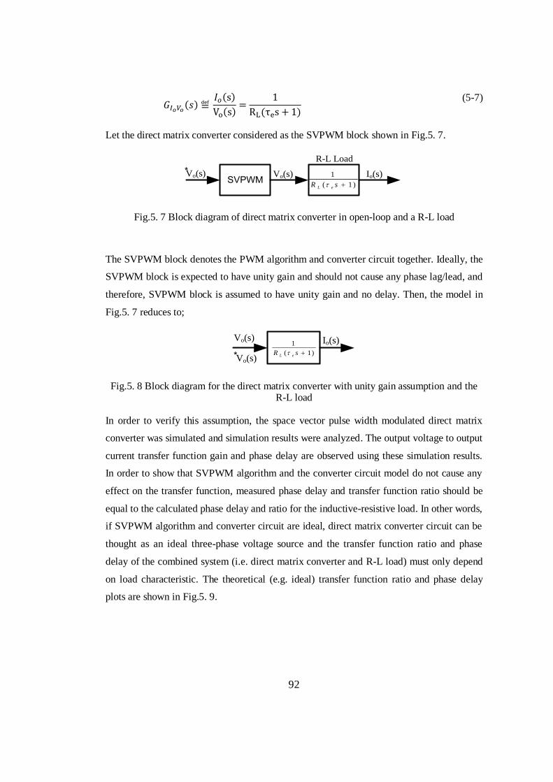
Fig.5. 7 Block diagram of direct matrix converter in open-loop and a R-L load ............................... 92
Fig.5. 8 Block diagram for the direct matrix converter with unity gain assumption and the R-L load
.................................................................................................................................................. 92
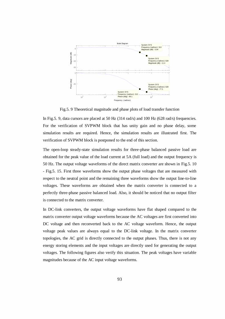
Fig.5. 9 Theoretical magnitude and phase plots of load transfer function .......................................... 93
Fig.5. 10 Output phase “a” to neutral voltage, Van (fo = 50 Hz) ......................................................... 94
Fig.5. 11 Output phase “b” to neutral voltage, Vbn (fo = 50 Hz)......................................................... 94
Fig.5. 12 Output phase “c” to neutral voltage, Vcn (fo = 50 Hz) ......................................................... 95
Fig.5. 13 Output line-to-line voltage Vab (fo = 50 Hz) ........................................................................ 95
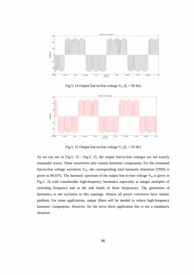
Fig.5. 14 Output line-to-line voltage Vbc (fo = 50 Hz) ........................................................................ 96
Fig.5. 15 Output line-to-line voltage Vca (fo = 50 Hz) ........................................................................ 96
Fig.5. 16 Harmonic spectrum of output line-to-line voltage Vab (fo = 50 Hz) .................................... 97
Fig.5. 17 Waveforms of the load currents (fo = 50 Hz) ...................................................................... 97
Fig.5. 18 Harmonic spectrum of the output phase “a” current (fo = 50 Hz) ....................................... 98
Fig.5. 19 Output phase “a” to neutral voltage, Van (fo = 100 Hz) ....................................................... 99
Fig.5. 20 Output line-to-line voltage Vab (fo = 100 Hz) ...................................................................... 99
Fig.5. 21 Harmonic spectrum of output line-to-line voltage Vab (fo = 100 Hz) .................................. 99
Fig.5. 22 Waveforms of the load currents (fo = 100 Hz) .................................................................. 100
Fig.5. 23 Harmonic spectrum of the output phase “a” current (fo = 100 Hz) ................................... 100
Fig.5. 24 Reference and observed output line-to-line voltage waveform, Vab ................................. 102
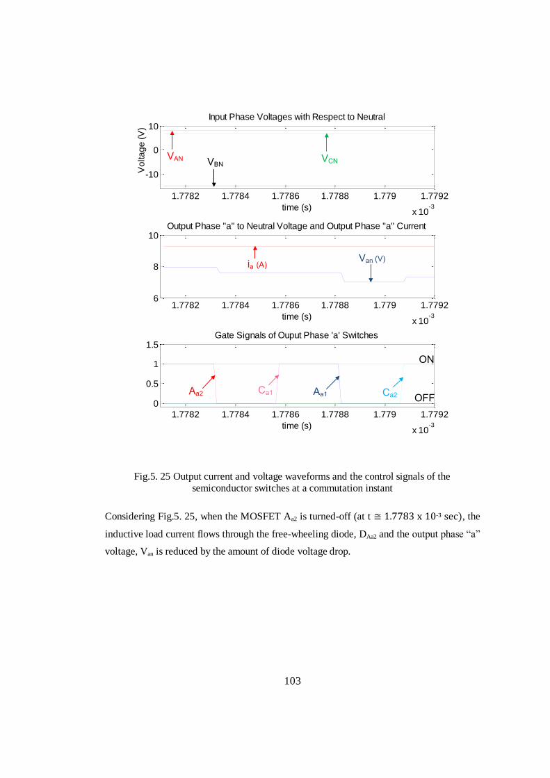
Fig.5. 25 Output current and voltage waveforms and the control signals of the semiconductor
switches at a commutation instant .......................................................................................... 103
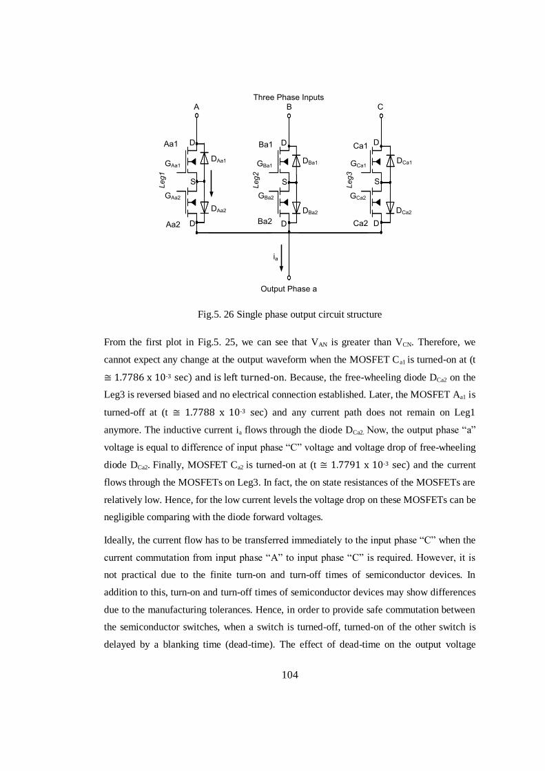
Fig.5. 26 Single phase output circuit structure ................................................................................. 104
Fig.5. 27 Block diagram of the closed-loop system involving the direct matrix converter with RL
load ......................................................................................................................................... 105
Fig.5. 28 Simple block diagram form of closed-loop direct matrix converter control system ......... 105
Fig.5. 29 Output phase “a” to neutral voltage, Van (fo = 50 Hz) ....................................................... 106
Fig.5. 30 Output line-to-line voltage Vab (fo = 50 Hz) ...................................................................... 107
Fig.5. 31 Close-loop output currents (fo = 50 Hz) ............................................................................ 107
Page 16
xvi
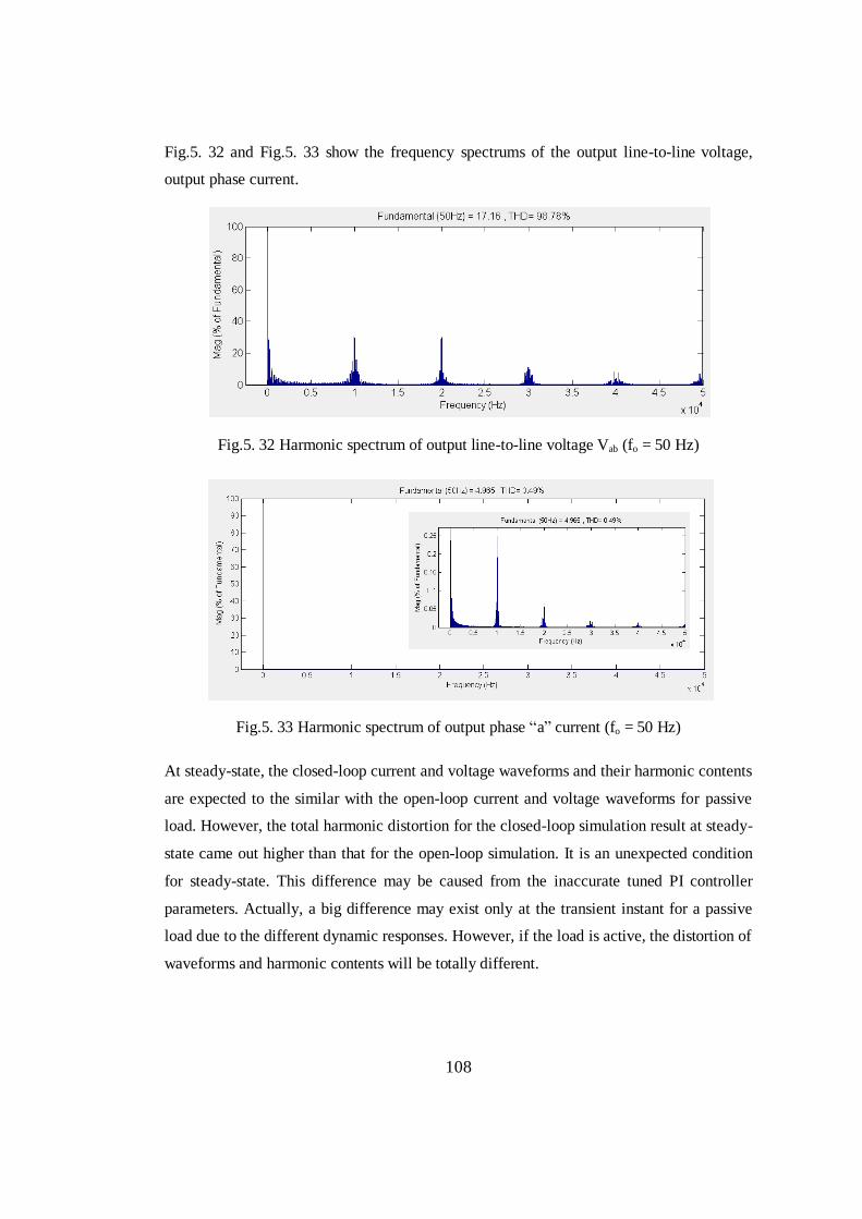
Fig.5. 32 Harmonic spectrum of output line-to-line voltage Vab (fo = 50 Hz) .................................. 108
Fig.5. 33 Harmonic spectrum of output phase “a” current (fo = 50 Hz) ........................................... 108
Fig.5. 34 Output phase “a” to neutral voltage, Van (fo = 100 Hz) ..................................................... 109
Fig.5. 35 Output line-to-line voltage Vab (fo = 100 Hz) .................................................................... 109
Fig.5. 36 Harmonic spectrum of output line-to-line voltage Vab (fo = 100 Hz) ................................ 110
Fig.5. 37 Closed-loop output currents (fo = 100 Hz) ........................................................................ 110
Fig.5. 38 Harmonic spectrum of output phase “a” current (fo = 100 Hz) ......................................... 110
Fig.5. 39 Unfiltered and filtered input phase “A” current vs. input phase “A” voltage, VAN ........... 111
Fig.5. 40 Harmonic spectrum of unfiltered input phase current, IA .................................................. 112
Fig.5. 41 Harmonic spectrum of filtered input phase current, IA ...................................................... 112
Fig.5. 42 Output phase “a” to neutral voltage, Van (fo = 50 Hz) ....................................................... 113
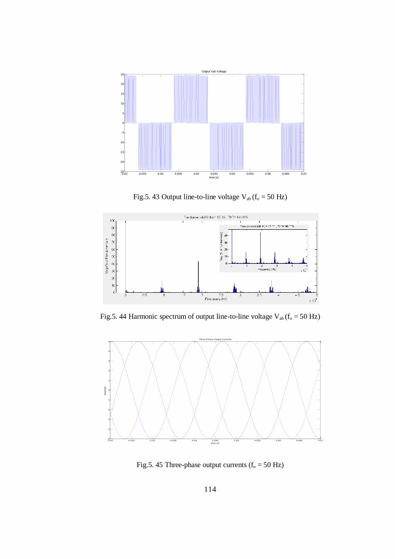
Fig.5. 43 Output line-to-line voltage Vab (fo = 50 Hz) ...................................................................... 114
Fig.5. 44 Harmonic spectrum of output line-to-line voltage Vab (fo = 50 Hz) .................................. 114
Fig.5. 45 Three-phase output currents (fo = 50 Hz) .......................................................................... 114
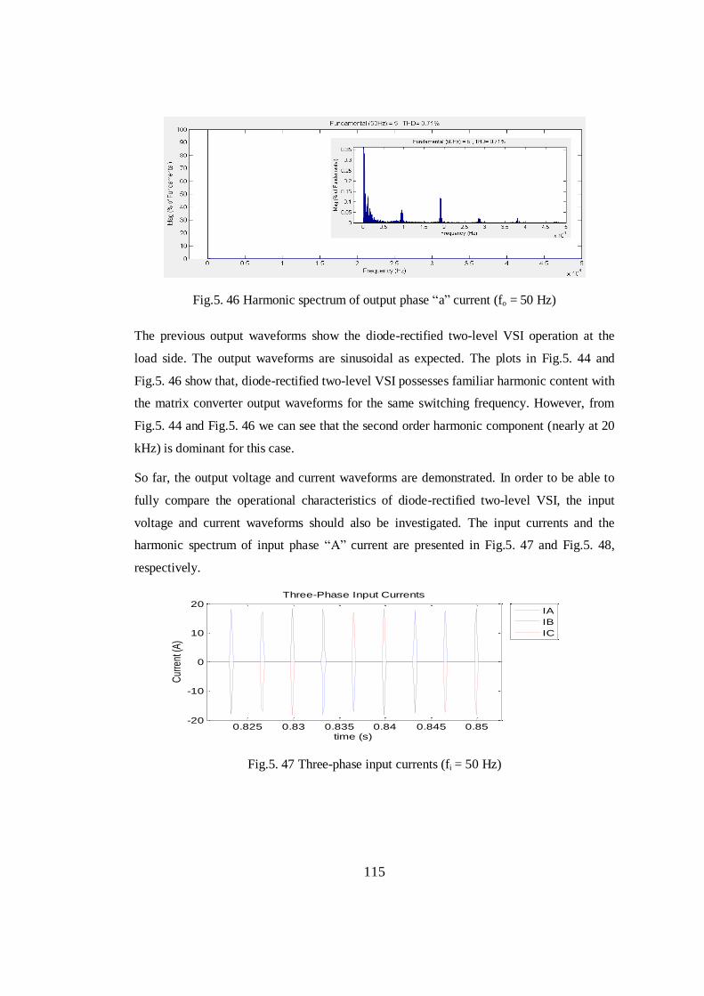
Fig.5. 46 Harmonic spectrum of output phase “a” current (fo = 50 Hz) ........................................... 115
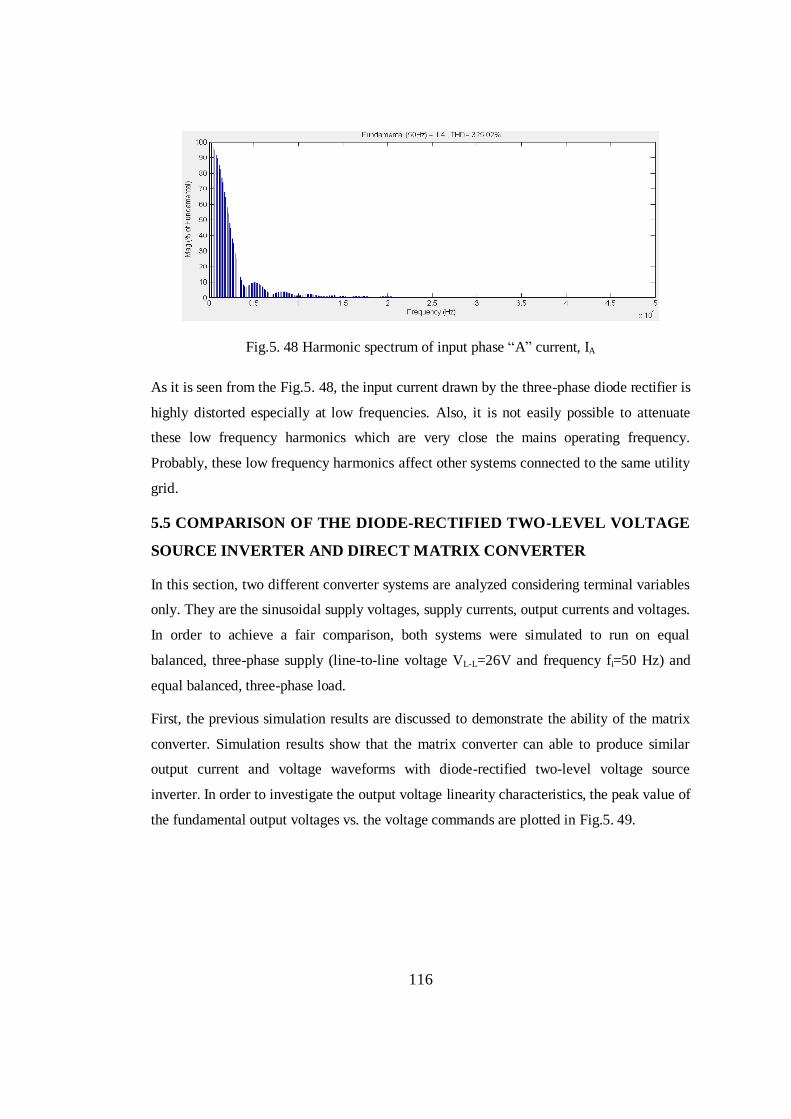
Fig.5. 47 Three-phase input currents (fi = 50 Hz) ............................................................................ 115
Fig.5. 48 Harmonic spectrum of input phase “A” current, IA ........................................................... 116
Fig.5. 49 Voltage linearity characteristics ........................................................................................ 117
Fig.5. 50 Basic scheme of FOC for permanent magnet synchronous motor .................................... 120
Fig.5. 51 Simulation model of the stator windings........................................................................... 122
Fig.5. 52 One-phase equivalent circuit model of SMPMSM ........................................................... 123
Fig.5. 53 Block diagram of closed-loop drive control system .......................................................... 124
Fig.5. 54 Dynamic responses of d-axis (id) and q-axis (iq) currents ................................................. 125
Fig.5. 55 Zoomed-in view of iq reference and iq .............................................................................. 125
Fig.5. 56 Output phase “a” to neutral voltage, Van (fo = 5.5 Hz) ...................................................... 126
Fig.5. 57 Output line-to-line voltage, Vab (fo = 5.5 Hz) .................................................................... 126
Fig.5. 58 Closed-loop three-phase output currents (fo = 5.5 Hz) ...................................................... 127
Fig.5. 59 Developed electromechanical motor torque and three-phase motor currents ................... 127
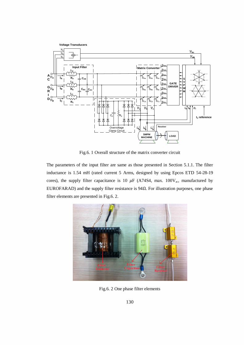
Fig.6. 1 Overall structure of the matrix converter circuit ................................................................. 130
Fig.6. 2 One phase filter elements .................................................................................................... 130
Fig.6. 3 Photograph of power circuit board ...................................................................................... 131
Fig.6. 4 Top view of gate-driver board............................................................................................. 133
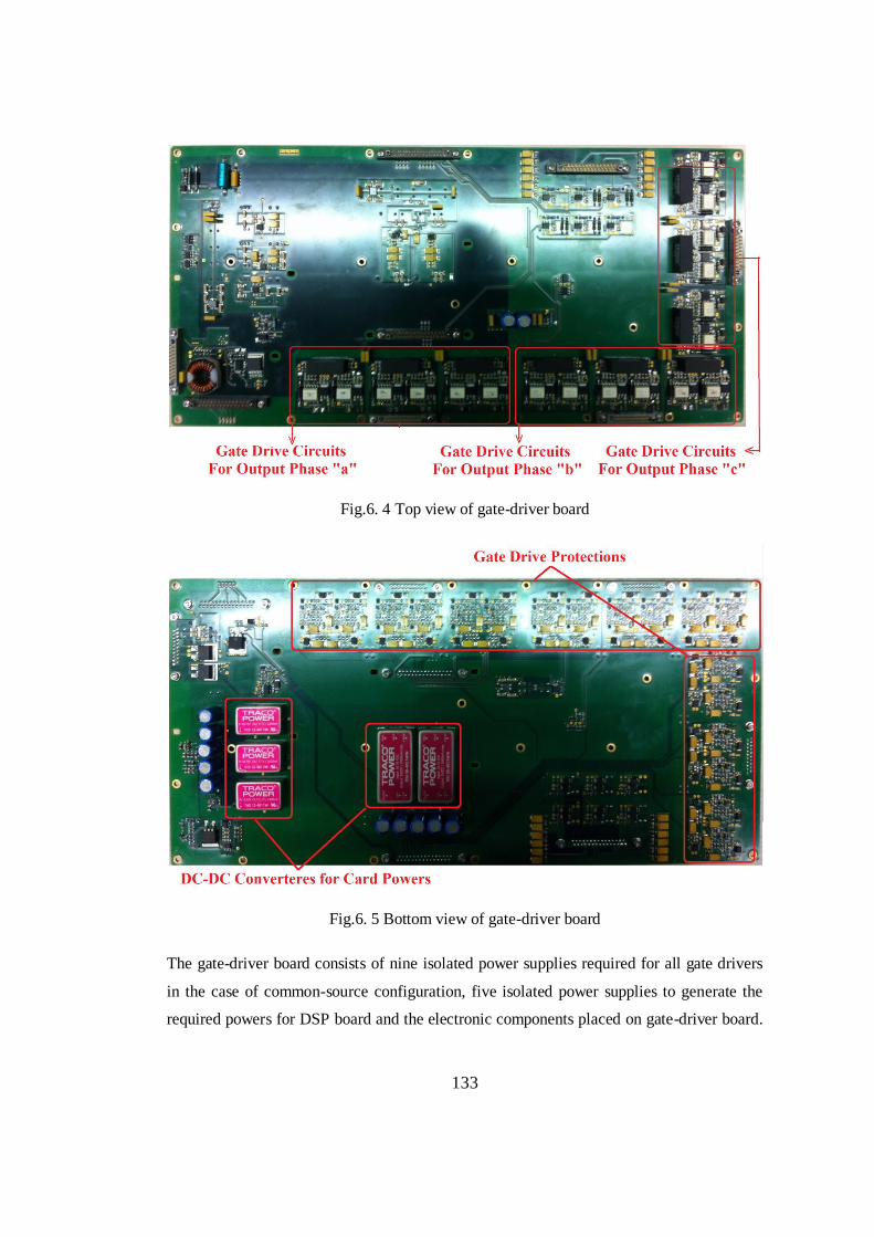
Fig.6. 5 Bottom view of gate-driver board ....................................................................................... 133
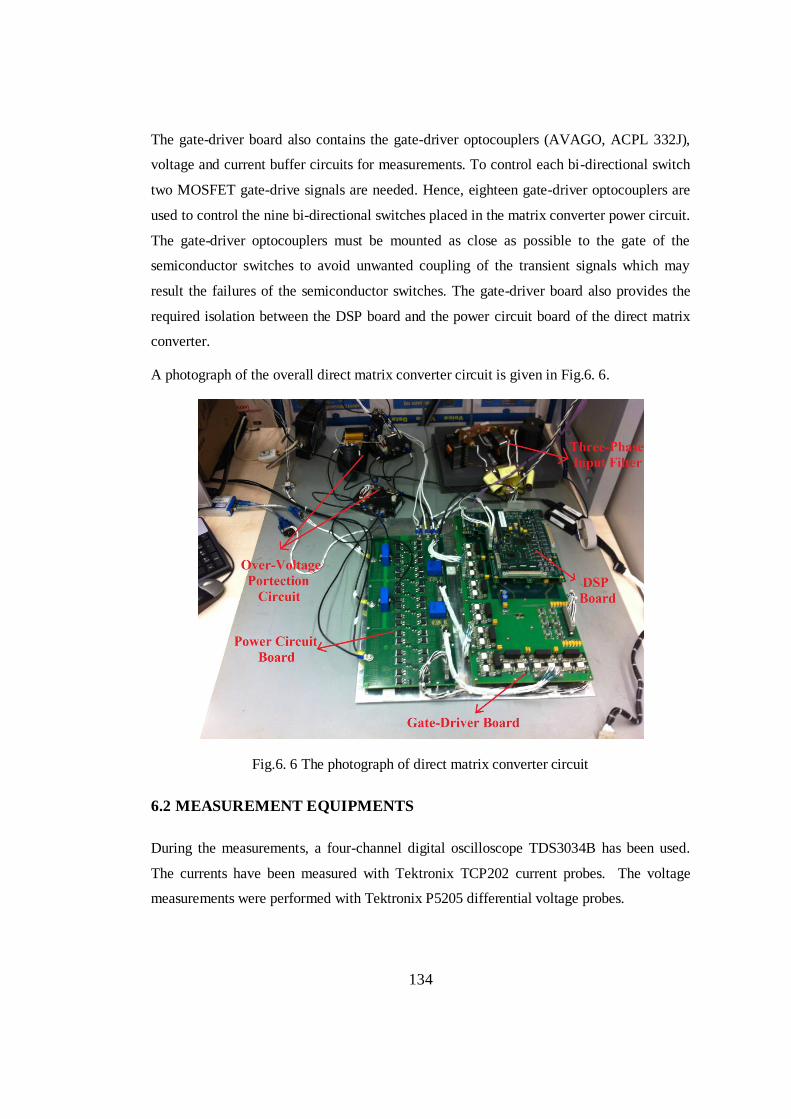
Fig.6. 6 The photograph of direct matrix converter circuit .............................................................. 134
Fig.6. 7 Output phase “a” to neutral voltage, Van (fo = 50 Hz) ......................................................... 136
Fig.6. 8 Output line-to-line voltage Vab (fo = 50 Hz) ........................................................................ 137
Page 17
xvii
Fig.6. 9 Harmonic spectrum of output line-to-line voltage Vab (fo = 50 Hz) .................................... 137
Fig.6. 10 Three-phase output currents (fo = 50 Hz) .......................................................................... 138
Fig.6. 11 Harmonic spectrum of the output phase “a” current (fo = 50 Hz) ..................................... 138
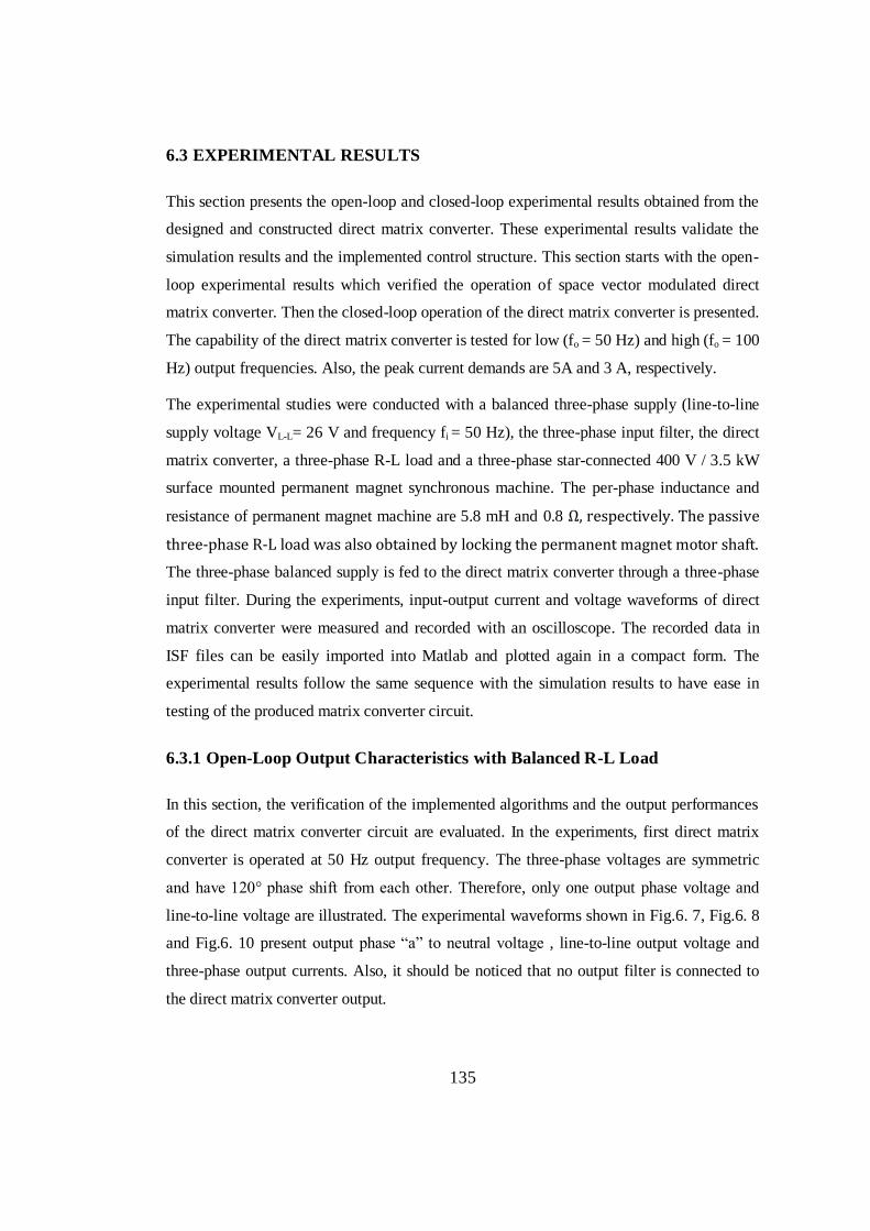
Fig.6. 12 Output phase “a” to neutral voltage, Van (fo = 100 Hz) ..................................................... 139
Fig.6. 13 Output line-to-line voltage Vab (fo = 100 Hz) .................................................................... 139
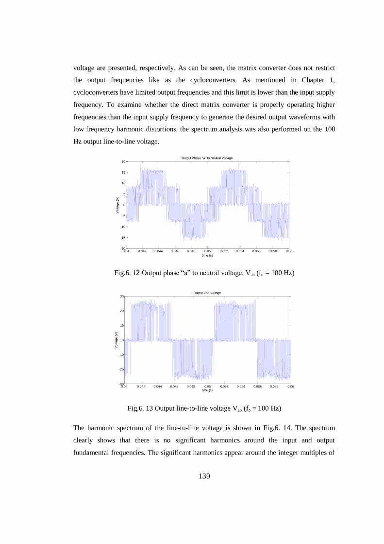
Fig.6. 14 Harmonic spectrum of output line-to-line voltage Vab (fo = 100 Hz) ................................ 140
Fig.6. 15 Three-phase output currents (fo = 100 Hz) ........................................................................ 140
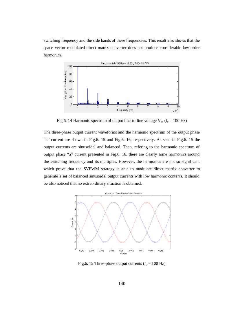
Fig.6. 16 Harmonic spectrum of the output phase “a” current (fo = 100 Hz) ................................... 141
Fig.6. 17 Dynamic responses of the matrix converter circuit ........................................................... 142
Fig.6. 18 Output phase “a” to neutral voltage, Van (fo = 50 Hz) ....................................................... 143
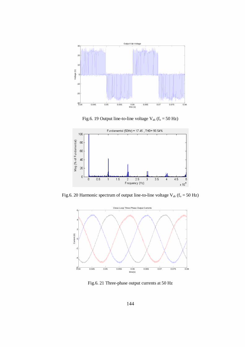
Fig.6. 19 Output line-to-line voltage Vab (fo = 50 Hz) ...................................................................... 144
Fig.6. 20 Harmonic spectrum of output line-to-line voltage Vab (fo = 50 Hz) .................................. 144
Fig.6. 21 Three-phase output currents at 50 Hz ............................................................................... 144
Fig.6. 22 Harmonic spectrum of the output phase “a” current (fo = 50 Hz) ..................................... 145
Fig.6. 23 Output phase “a” to neutral voltage, Van (fo = 100 Hz) ..................................................... 146
Fig.6. 24 Output line-to-line voltage Vab (fo = 100 Hz) .................................................................... 146
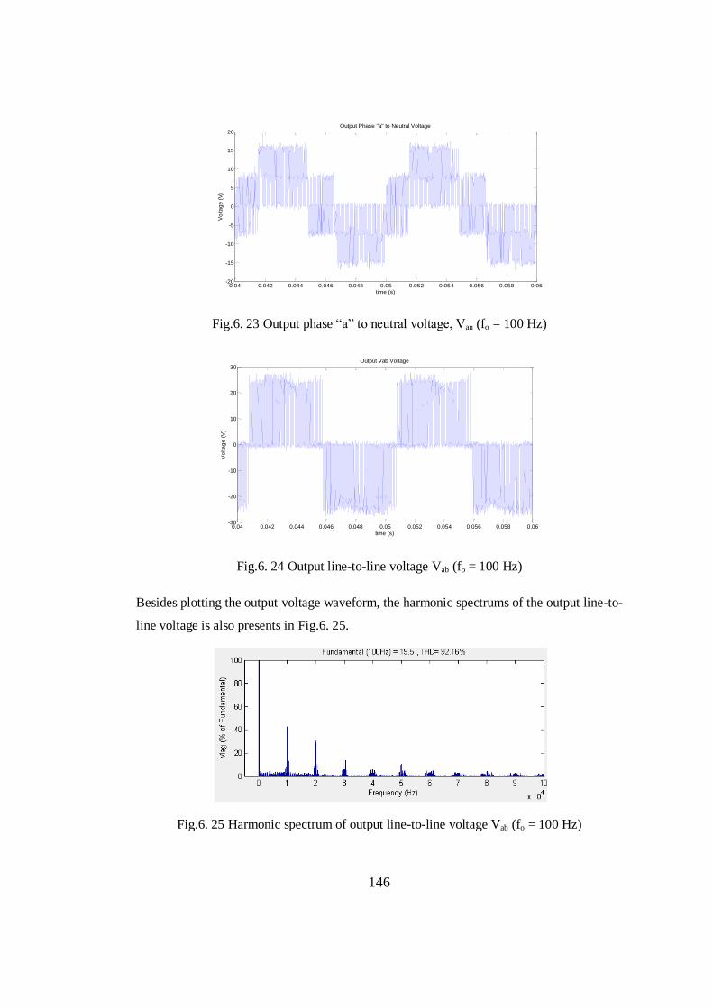
Fig.6. 25 Harmonic spectrum of output line-to-line voltage Vab (fo = 100 Hz) ................................ 146
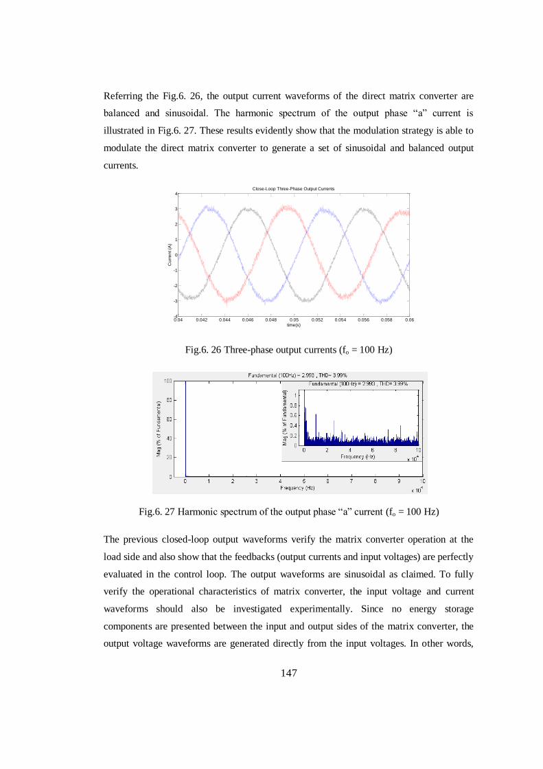
Fig.6. 26 Three-phase output currents (fo = 100 Hz) ........................................................................ 147
Fig.6. 27 Harmonic spectrum of the output phase “a” current (fo = 100 Hz) ................................... 147
Fig.6. 28 Input phase “A” to neutral voltage, VAN and unfiltered input current, IA.......................... 148
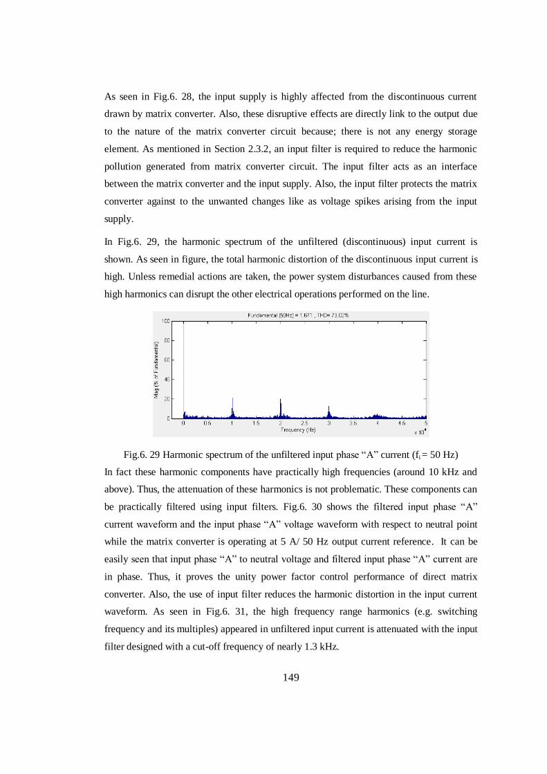
Fig.6. 29 Harmonic spectrum of the unfiltered input phase “A” current (fi = 50 Hz) ...................... 149
Fig.6. 30 Input phase “A” to neutral voltage, VAN and filtered input current, IA (fi =50 Hz) ........... 150
Fig.6. 31 Harmonic spectrum of the filtered input phase “A” current (fi = 50 Hz) .......................... 150
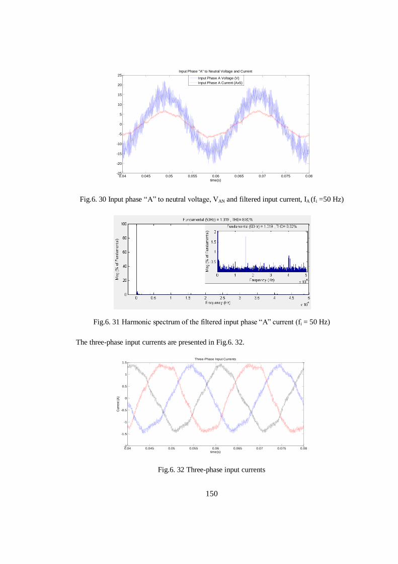
Fig.6. 32 Three-phase input currents ................................................................................................ 150
Fig.6. 33 Output phase “a” to neutral voltage, Van (fo = 5.5 Hz) ...................................................... 152
Fig.6. 34 Output line-to-line voltage Vab (fo = 5.5 Hz) ..................................................................... 152
Fig.6. 35 Three-phase output currents (fo = 5.5 Hz) ......................................................................... 153
Fig.6. 36 Developed motor torque and converter output currents .................................................... 153
Page 18
xviii
LIST OF TABLES
TABLES
Table 2. 1 The allowable current directions according to the switch state combinations................... 30
Table 2. 2 All switching combinations for current based commutation ............................................. 33
Table 4. 1 All possible safe switching configurations ........................................................................ 63
Table 4. 2 All allowed switching configurations and the corresponding DC-link voltage and input
line currents .............................................................................................................................. 68
Table 4. 3 All allowable switching configurations for the inversion stage ........................................ 72
Table 4. 4 Sector pairs and useable vectors ........................................................................................ 79
Table 5. 1 Simulation parameters ....................................................................................................... 90
Table 5. 2 Calculated theoretical gain and phase angles for R-L load ............................................. 101
Table 5. 3 Parameters of the test motor ............................................................................................ 122
Page 19
xix
LIST OF ABBREVIATIONS
AC : Alternating Current
DC : Direct Current
DMC : Direct Matrix Converter
FOC : Field Oriented Control
IGBT : Insulated Gate Bipolar Transistor
IGCT : Integrated Gate Commutated Thyristor
IMC : Indirect Matrix Converter
IPM : Interior Permanent Magnet
MC : Matrix Converter
MMF : Magneto Motive Force
MOSFET : Metal Oxide Semiconductor Field Effect Transistor
PCB : Printed Circuit Board
PI : Proportional Integral
PWM : Pulse Width Modulation
SPWM : Sinusoidal Pulse Width Modulation
SMPM : Surface Mounted Permanent Magnet
SVPWM : Space Vector Pulse Width Modulation
THD : Total Harmonic Distortion
VSI : Voltage Source Inverter
Page 20
xx
NOMENCLATURE
VA, VB, VC : Three-Phase Input Voltages
, , : Instantaneous Input Phase Voltages
VAB, VBC, VCA : Line-to-Line Input Voltages
, , : Instantaneous Line-to-Line Input Voltages
: Peak Value of Input Line-to-Line Voltages
: Peak Value of Three-Phase Input Currents
: Input Angular Frequency
: Angle between Input Phase Voltages and Currents
iA, iB, iC : Three-Phase Input Currents
, , : Instantaneous Input Line Currents
Va, Vb, Vc : Three-Phase Output Voltages
, , : Instantaneous Output Phase Voltages
Vab, Vbc, Vca : Line-to-Line Output Voltages
ia, ib, ic : Three-Phase Output Currents
, , : Instantaneous Output Phase Currents
: Peak Value of Output Phase Voltages
: Peak Value of Output Phase Currents
: Output Angular Frequency
: Angle between Output Phase Voltages and Currents
VDC : Mean Value of DC-link Voltage
IDC : Mean Value of DC-link Current
Cp : Clamp Capacitor
Rp : Clamp Resistor
CAB, CBC, CAC : Input Filter Capacitors
LA, LB, LC : Input Filter Inductors
RA, RB, RC : Input Filter Resistors
Rf : Input Filter Resistance
Lf : Input Filter Inductance
Cf : Input Filter Capacitance
S : Switch State
Page 21
xxi
: Output Power
: Input Power
: Total Copper Loss
pout : Instantaneous Value of Output Power
pin : Instantaneous Value of Input Power
Ea : Rms Value of Back-emf Voltage
: Electrical Rotor Speed
: Angular Velocity of Motor
p : Pole Number
f : Permanent Magnet Flux Linkage
q : Quadrature Axis Stator Flux Linkage
d : Direct Axis Stator Flux Linkage
m : Magnet Flux Linkage
La, Lb, Lc : Self Inductances of Stator Windings
Ra, Rb, Rc : Stator Winding Resistances
Lab, Lba, Lca, Lac, Lbc, Lcb, M : Mutual Inductances
Rs : Per-Phase Equivalent Stator Winding Resistance
Ls : Per-Phase Equivalent Stator Winding Inductance
ea, eb, ec : Phase Back-emf Voltages
: Direct Axis Inductance
: Quadrature Axis Inductance
: Quadrature Axis Voltage
: Direct Axis Voltage
: Rotating Quadrature Axis Stator Current
: Rotating Direct Axis Stator Current
: Angle between Induced Back-emf and Stator Current
: Angle between Stator Phase Voltage and Current
: Modulation Matrix
q : Input to Output Voltage Transfer Ratio
, , : Three Variables of Balanced Three-Phase System
: Input Phase Voltage Vector
: Output Phase Voltage Vector
Page 22
xxii
: Input Line Current Vector
: Output Phase Current Vector
i : Angle of Input Voltage Vector
o : Angle of Output Voltage Vector
i : Angle of Input Current Vector
o : Angle of Output Current Vector
dx, dy : Duty Ratios of Input Current Vectors
d , d : Duty Ratios of Output Voltage Vectors
: Duty Ratio of Zero Current Vectors
: Duty Ratio of Zero Voltage Vectors
, : Applied Time Durations of Active Current Vectors
: Applied Time Duration of Zero Current Vectors
, : Applied Time Durations of Active Voltage Vectors
: Applied Time Duration of Zero Voltage Vectors
d0 : Duty Ratio of Zero Vectors
RL : Per-Phase Load Resistor
LL : Per-Phase Load Inductor
fs : Switching Frequency
fo : Output Frequency
fi : Input Supply Frequency
Ts : Switching Period
Kp : Proportional Gain
Ki : Integrator Gain
pu : Per-Unit
N : Neutral Point of Input Supply
n : Neutral Point of Output
: Output Voltage to Output Current Transfer Function
: Output Current Reference to Output Current Transfer
Function
mc : Current Modulation Index
mv : Voltage Modulation Index
: Transfer Function of Direct Matrix Converter
Page 23
xxiii
: Transfer Function of Two-level Voltage Source Inverter
: Transfer Function of Voltage Source Rectifier
: Filter Cut-off Frequency
vo(t) : Instantaneous Output Voltage
io(t) : Instantaneous Output Current
Page 24
1
CHAPTER 1
INTRODUCTION
Electrical energy is widely utilized from low to high power areas in numerous modern
industrial and domestic applications in the world. However, in many applications, the AC
mains power cannot be directly utilized. For example, in variable speed drives, in order to
run AC motors at different speeds; it is necessary to have a variable frequency and
amplitude AC power supply. Also in order to run DC motor at different speeds; AC/DC
power conversion is necessary. Hence, many parts of industrial application require power
conversions. In the past, DC motors had been widely preferred since the torque of a DC
motor can be easily controlled. Today, DC motors are replaced by AC motors because of
the maintenance problems of DC motors due to the presence of commutators and brushes.
As a result, AC motor drives have gained substantial attention. In order to effectively
control the AC motors, many special devices that maintain the AC/AC power conversion
process, have been designed and produced.
1.1 AC/AC POWER CONVERSION
The variable AC electrical power should be achieved through AC/AC power conversion
from utility AC power with fixed amplitude and frequency. AC/AC converters take power
from an AC system and deliver it to another with waveforms of adjustable amplitudes and
frequencies.
Nowadays, various power converter circuits are used which improve the performance,
efficiency and reliability of the systems they take place. Fig.1. 1 displays a classification of
converter families used in electrical drive applications. The AC/AC converters are
classified into two groups such as; indirect (DC-link) converters which include DC-link
Page 25
2
components between the two AC systems and direct converters that provide direct AC/AC
power conversion.
Low-to-High Power
Drives
Direct ConvertersIndirect (DC-Link)
Converters
Cycloconverters Matrix ConvertersDiode Rectified Current
Source Inverters
Diode Rectified Voltage
Source Inverters
Two-Level Voltage
Source InvertersMultilevel InvertersTwo-Level Matrix
Converters
Multilevel Matrix
Converters
PWM Rectifier-Voltage
Source Inverters
Fig.1. 1 Classifications of converters low-to-high power drives
In all indirect power converter circuits, diode-rectified two-level voltage source inverters
(VSI) are totally widespread nowadays. VSI is a DC/AC converter that generates AC
output voltages from a DC input voltage. Three-phase two-level VSI shown in Fig.1. 2, is
one of the most widely used inverter topology for three-phase applications.
Idc
ib ic
S1
ia
S2
S3
S4
S5
S6
D1
D2
D3
D4
D5
D6
VDC
+
-
Fig.1. 2 Three-phase two-level voltage source inverter circuit topology
In direct AC/AC converters, the cycloconverter is the most commonly employed topology
in three-phase to three-phase applications, which uses semiconductor switches to connect
directly the power supply to the load, converting a three-phase AC voltage to a three-phase
AC voltage with adjustable magnitude and variable frequency. It allows power flow in
either direction. The operating output frequency of this direct converter should be less than
Page 26
3
the input frequency. In addition to the cycloconverters, matrix converters have enjoyed
increasing interest as direct converters in recent years. This interest is reflected in the
number of articles and papers written about matrix converters in the last ten years.
1.1.1 Overview of Indirect (DC-link) Two-Level Voltage Source Converters
As mentioned earlier, two-level voltage source inverter is a DC/AC converter. However,
DC voltage is not common voltage. To generate DC voltage, rectifier structures are
commonly used. A rectifier is a device that converts alternating voltage to direct voltage.
This process is also called as rectification. The most commonly used rectifier structure is
three-phase diode rectifier shown in Fig.1. 3. The circuit also contains a DC-link capacitor
to ensure ripple free DC-link voltage.
iA iB iCC
VA VB VC
VDC
+
-
D7
D8
D9
D10
D11
D12
Fig.1. 3 Diode rectifier stage
Most of the converters use diode-rectifiers (followed by a DC-link capacitor), which draw
non-sinusoidal currents (iA, iB, iC) even when fed with a balanced sinusoidal voltages
(VA,VB,VC). Only considering the load side currents (ia, ib, ic), the diode rectifier based VSI
may be is a good solution, but its supply side currents (iA, iB, iC) are highly distorted,
containing high amounts of low order harmonics which may further interfere with the other
electric systems in the network. In addition, the current flow on diodes cannot be reversed.
Thus, bi-directional power flow cannot be provided without using an auxiliary circuit. This
is another drawback of this topology. Fig.1. 4 represents the diode rectifier based VSI
structure.
Page 27
4
Idc
ib ic
S1
ia
S2
S3
S4
S5
S6
D1
D2
D3
D4
D5
D6
iA iB iCC
VA VB VC
VDC
+
-
D7
D8
D9
D10
D11
D12
Fig.1. 4 Diode rectifier based VSI
A conventional solution for the harmonics in input current waveforms and bi-directional
power flow problems is to use a controlled bridge rectifier instead of diode rectifier as
shown in Fig.1. 5. This structure is called back-to-back voltage source converter (BBVSC).
The BBVSC was introduced in the late 1970s. The BBVSC draws sinusoidal current
waveforms (iA, iB, iC) from the AC supply. It contains a DC-link capacitor between
controlled bridge rectifier and the inverter bridge and supply filter inductors.
The DC-link capacitor is a bulky component with a limited lifetime. Moreover, supply filter
inductors (Ls) placed at the input terminals of the controlled bridge rectifier are also bulkier
and heavier than the DC-link capacitor in low and medium power conversion. Therefore,
this conventional indirect converter has also big volume.
Idc
ib ic
S7
ia
S8
S9
S10
S11
S12
iA
C
VA VB VC
VDC
+
-
D7
D8
D9
D10
D11
D12
S1
S2
S3
S4
S5
S6
D1
D2
D3
D4
D5
D6
iB iC
LS1 LS2 LS3
Fig.1. 5 Back to back voltage source converter
Page 28
5
1.1.2 History of Direct AC/AC Converters
The idea of direct frequency conversion was originally presented in the 1920s [1]. In
general, direct AC/AC converters can be classified in two distinct groups. Converters in the
first group are those which can be used if the operating output frequencies are lower than
the input supply frequency. This converter was called cycloconverter. It converts AC
voltage waveforms, such as that of the main supply, to other AC voltage waveforms with
lower frequency. After the invention of thyristor, the first semiconductor based
cycloconverter were developed in the 1960s [2]. A possible typical phase-controlled
thyristor-based three-phase to three-phase cycloconverter is displayed in Fig.1. 6.
VA
VB
VC
Th
ree
Ph
ase
Ba
lan
ce
d L
oa
d
Phase a
Phase b
Phase c
i a
i b
i c
Three Phase
Power Supply
Output
Side
Input
Sidei C
i B
i A
Fig.1. 6 Phase-controlled thyristor-based three-phase to three-phase cycloconverter
They are commonly employed in three-phase applications. In most power systems, the
amplitude and the frequency of input voltage applied to a cycloconverter have fixed
magnitudes, whereas both the amplitude and the frequency of output waveforms of a
cycloconverter tend to be variable. The load voltage and input current waveforms in the
cycloconverter are heavily distorted and power factor of the input is quite poor. However,
the quality of the output waveforms can be enhanced if more switching devices are
employed [2]. Moreover, its output frequency is also usually limited to half frequency of the
Page 29
6
input supply. Because, normal loads cannot tolerate the voltage distortion produced with
higher input to output frequency ratios. Thus, the only advantages remaining are robustness
of the thyristor and low losses.
Considering all mentioned above, the cycloconverter cannot be seen as an optimal solution
for low and medium power level converters because of restricted output frequencies and
poor harmonic performance. However, for the high power levels, cycloconverter can be
seen as an optimal solution due to the low loses and robustness.
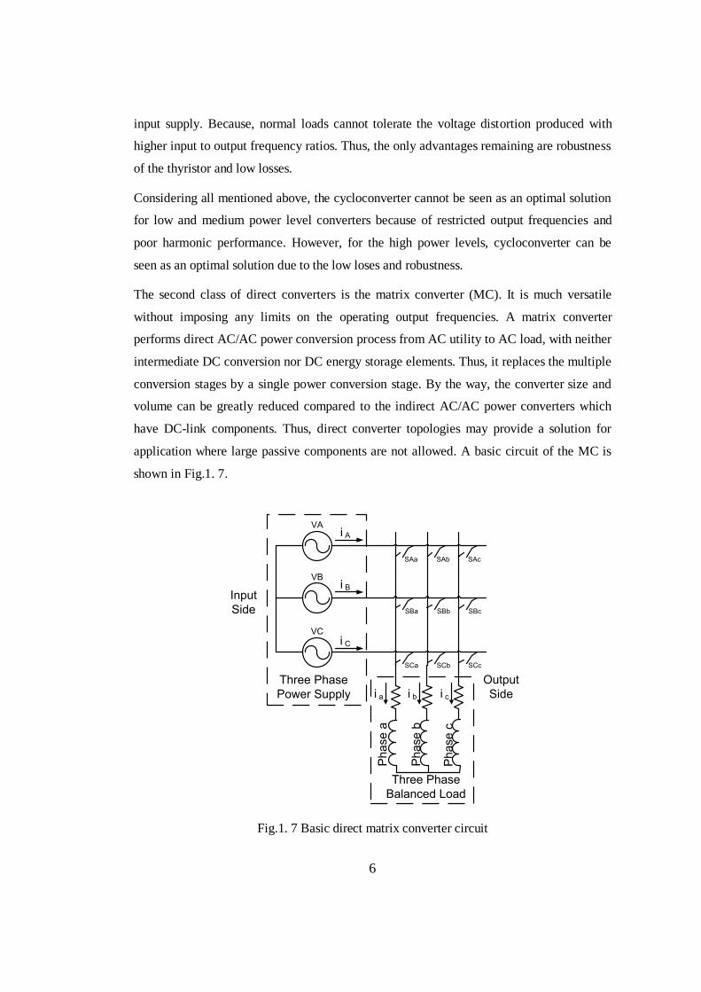
The second class of direct converters is the matrix converter (MC). It is much versatile
without imposing any limits on the operating output frequencies. A matrix converter
performs direct AC/AC power conversion process from AC utility to AC load, with neither
intermediate DC conversion nor DC energy storage elements. Thus, it replaces the multiple
conversion stages by a single power conversion stage. By the way, the converter size and
volume can be greatly reduced compared to the indirect AC/AC power converters which
have DC-link components. Thus, direct converter topologies may provide a solution for
application where large passive components are not allowed. A basic circuit of the MC is
shown in Fig.1. 7.
VA
VB
VC
SAa SAcSAb
SBa SBcSBb
SCa SCcSCb
Three Phase
Balanced Load
Ph
ase
a
Ph
ase
b
Ph
ase
c
i a i b i c
Three Phase
Power Supply
Output
Side
Input
Side
i A
i B
i C
Fig.1. 7 Basic direct matrix converter circuit
Page 30
7
1.1.3 Concept of Matrix Converter
MC is basically a switch-mode direct AC/AC power conversion device without requiring
the use of a bulky storage electrolytic capacitor. They are gaining considerable attention as
an alternative to the classical structures such as back-to-back voltage source converters and
diode-rectified two-level voltage source inverters, due to the system level advantages such
as; the possibility to increase the power density of the power conversion system; inherent
four-quadrant operation capability; allowing bi-directional power flow; producing
sinusoidal input and output current waveforms (low harmonic contents in the input
currents); controllability of the input power factor; and increasing the reliability and
compact design [3].
The matrix converter topology consists of controlled bi-directional switches which directly
connect the load to the source. Hence, in this converter input and output sides are directly
linked. The output voltage and current waveforms with adjustable magnitude and frequency
are constructed by single-stage power conversion process. The single stage power
conversion principle has given distinct structure to the matrix converter. This aspect makes
the modulation control of the matrix converter quite different and complicated. However,
the matrix converter topology can be implemented with much compact in size and volume
compared with the diode-rectifier based two-level VSI and back-to-back voltage source
converter. In addition to its compact design, it draws sinusoidal input currents with unity
power factor as well as sinusoidal output currents and the matrix converter can operate at
high temperature surroundings due to the lacking of DC-link capacitors, which is very
vulnerable in high temperature. Therefore, the converter also has longer lifetime.
Considering these advantages, the matrix converters have become increasingly attractive
for AC/AC power conversion.
In practice, an input filter is also necessary to attenuate the input currents harmonics. This
can be interpreted as a realistic advantage if the filter size is also optimized, by employing
the semiconductor devices with sufficiently high switching frequency. This means that a
consensus between the size of input filter and the semiconductor losses must be found.
Considering all factors mentioned above which are fundamental for good power supply and
electric drive applications. The main feature of this converter is to allow these
fundamentals for power supply and electric drive applications.
Page 31
8
The matrix converters were first mentioned in the early 1980’s by Alesina and Venturini [4].
They developed a rigorous mathematical description of matrix converter and presented the
concept of the duty-cycle modulation matrix. This pulse width modulation method is
known as the Venturini Modulation method. Unfortunately, this method had a serious
drawback. The initial Venturini Modulation was limited to a maximum 50% input to output
voltage transfer ratio. They later proposed an improved method to increase this limit, thus
third harmonics were successfully included in the output voltage waveforms. The
maximum input voltage to output voltage transfer ratio became 86.6%.
A different waveform synthesis approach was proposed by P. Ziogas et al. in [2]. They split
the matrix converter into a fictitious rectifier and a fictitious inverter and instead of using
the matrix converter to assemble its output voltage directly from three-phase AC input
voltage; the input voltage was first rectified to create an imaginary DC-link voltage and
later inverted at the required output frequency. This technique was referred as the indirect
function approach and it allowed the use of well-known techniques for controlling the
fictitious rectifier and inverter.
Space vector pulse width modulation technique was first employed by Huber et al. in 1989
[5] which has been well established to obtain satisfactory input/output performance to
control a matrix converter. The modulation technique which employed space vectors in
both the rectifier and inverter process allows obtaining the maximum output to input
voltage ratio (0.86), sinusoidal input current and control of the input displacement factor.
1.2 SCOPE OF THESIS AND STRUCTURE OF CHAPTERS
This study focuses on closed-loop field oriented control of a surface mounted permanent
magnet synchronous motor using space vector modulated direct AC-AC matrix converter.
In this thesis, the first objective is to analyze the matrix converter topologies. The second
objective is to investigate the modulation methods and implement the most suitable one.
The other objective is to develop a matrix converter simulation model to demonstrate the
feasibility of developed algorithm. And the last objective is to design and produce a matrix
converter circuit and verify the converter operation.
This thesis is categorized in seven chapters in the following style.
Page 32
9
Chapter 1 gives the basic information about AC/AC power converters, their advantages and
disadvantages.
Chapter 2 presents the structure of matrix converter integrated permanent magnet drive
system, fundamentals of matrix converter topologies, input-output characteristics and
structures of matrix converters.
Chapter 3 focuses on the steady-state and dynamic modeling of permanent magnet
synchronous machines.
Chapter 4 gives the state-space equations of matrix converter terminal voltages and
currents. Then, matrix converter modulation methods are presented and space vector
definition is introduced. Finally, space vector modulation methods for matrix converter are
investigated in detail.
Chapter 5 demonstrates the modeling of the matrix converter system. Then, the open-loop
and closed-loop performances of direct matrix converter are investigated by the
simulations. The comparison of the direct matrix converter and the diode-rectified two-
level voltage source inverter is studied in simulations. Finally, the operational analysis of
matrix converter integrated surface mounted permanent magnet synchronous machine drive
system is presented.
Chapter 6 presents the conducted tests on matrix converter circuit using a passive R-L load
and a surface mounted permanent magnet synchronous machine. The operation of the direct
matrix converter system is examined based on the experimental results. During the tests, the
line-to-line supply voltage is set to 26 V peak value and a 400 V/3.5 kW surface mounted
permanent magnet motor is used.
Chapter 7 summarizes the overall study conducted in the thesis and concludes the
performance of the indirect space vector modulated direct AC/AC matrix converter.
Page 33
10
CHAPTER 2
THE PERMANENT MAGNET SYNCHRONOUS MACHINE (PMSM)
DRIVE SYSTEM USING DIRECT MATRIX CONVERTER
In this chapter, the structure of permanent magnet synchronous machine (PMSM) drive
system with matrix converter is presented first. After that, fundamentals of matrix converter
topology are introduced. That is followed by a presentation of input-output characteristics
of matrix converter. At the end of this chapter, structural issues of matrix converter are
investigated.
2.1 STRUCTURE OF PERMANENT MAGNET MACHINE DRIVE
SYSTEM
A permanent magnet synchronous machine, a power converter (i.e. only power stage) and a
controller (PWM is considered in controller) are the three major components of an
electrical drive system. The structure of a permanent magnet synchronous machine drive is
given in Fig.2. 1 in block diagrams. Parts of the block diagrams are also discussed in this
chapter.
Page 34
11
Three Phase
Power Supply
Power Converter PMSM
Controller
ia,ib,ic
r, Shaft
Position
Information
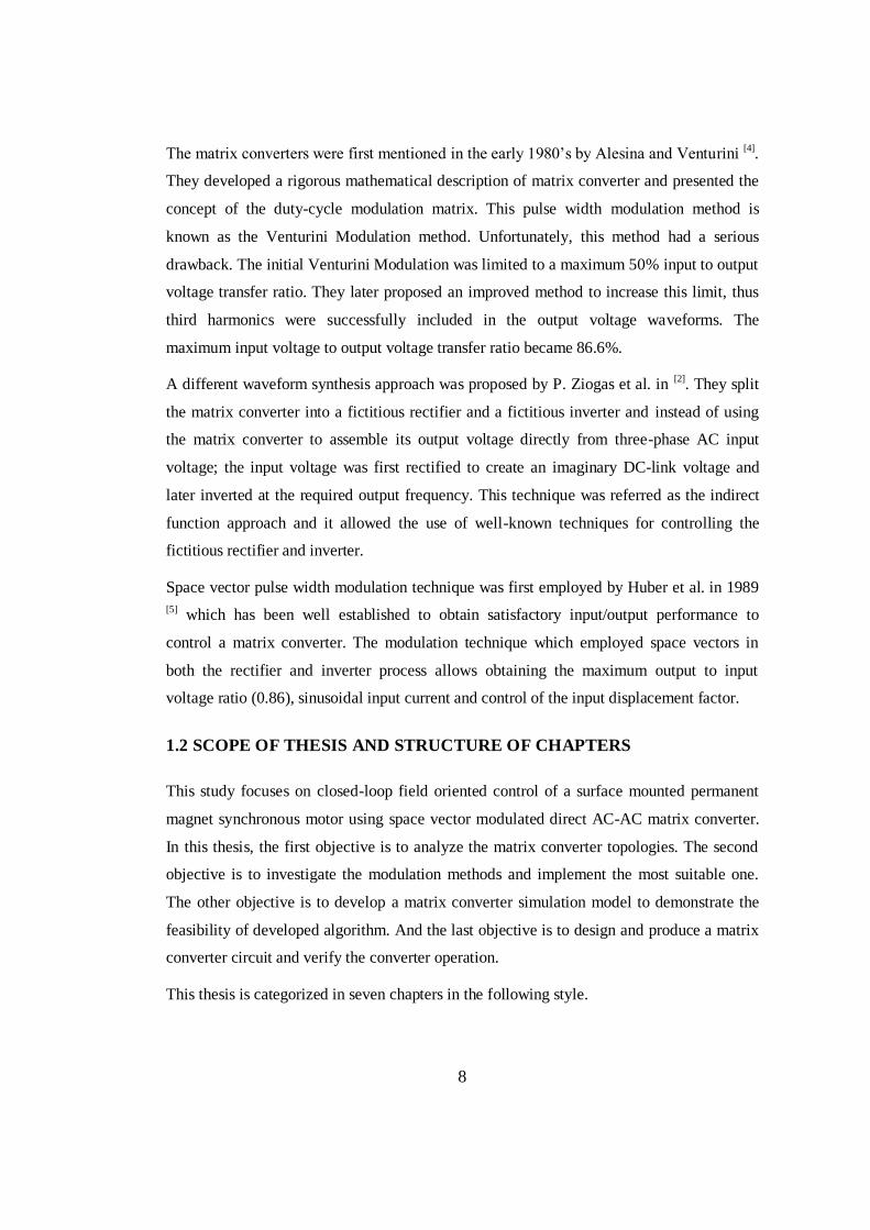
wr
User/External
Command
Fig.2. 1 PMSM drive basic architecture
The power converter typically involves a rectifier, DC-link capacitors, an inverter, gate
drivers for the power transistors placed in the inverter and current transducers.
The controller involves a microcontroller or a digital signal processor (DSP) and peripheral
interface circuits to gather the sensor data (e.g. data from current transducers and position
sensor).
In general, diode-rectified three-phase two-level PWM voltage source inverters drive the
permanent magnet synchronous machines. Besides that, matrix converters can also be used,
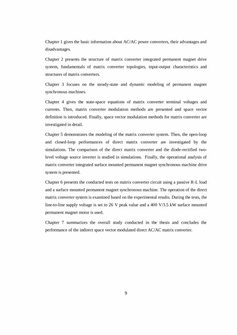
especially in high power density applications where the large electrolytic capacitors are
inappropriate. The block diagram of the permanent magnet synchronous machine drive
system with vector controlled matrix converter is presented in Fig.2. 2.
Matrix
ConverterPMSM
PWM DriverPLL Controller
ia ib r, Rotor
Position Angle
s, Input
Phase Angle
ia
ib
ic
Va
Vb
Vc
VA
VB
VC
iA
iB
iC
User/External Command
Input Filter
LC
Fig.2. 2 Block diagram of PMSM drive system
Page 35
12
2.2 FUNDAMENTALS OF MATRIX CONVERTER
The matrix converter is an alternative to the conventional AC-DC-to-DC-AC converter. It
has several advantages over them such as [6];
Matrix converter provides sinusoidal input current and output waveforms,
Matrix converter allows inherently bidirectional power flow,
Matrix converter allows inherently four-quadrant operation,
Matrix converter has compact design (e.g. small size) due to the absence of large
energy storing elements,
Matrix converter has the possibility to increase the power density of the power
conversion system,
Matrix converter has the capability of fully controlled input power factor.
The matrix converter has also disadvantages such as;
The input voltage to output voltage transfer ratio is 0.86,
Matrix converter is sensitive to the disturbances on the AC mains.
2.3 INPUT-OUTPUT CHARACTERISTICS OF MATRIX CONVERTER
This section presents a brief description of main characteristics of matrix converter.
2.3.1 Output Voltages and Currents
The matrix converter connects input lines to all three output lines for any desired time
duration. It does not need presence of any large energy storage elements between the input
and output sides as shown in Fig.2. 3.
Page 36
13
Input Filter
SAa SAcSAb
SBa SBcSBb
SCa SCcSCb
A
B
C
a b c
Matrix Converter
L
C
Fig.2. 3 Structure of matrix converter system
AC output voltage waveforms are synthesized directly from the AC input voltage
waveforms. Thus, the sampling and switching rate has to be set much higher than both of
the input and output frequencies. In Fig.2. 4, the line-to-line output voltage waveform for a
10 kHz switching frequency is shown [6]. The red colored waveform is the fundamental
component of the output line-to-line voltage.
Fig.2. 4 Line-to-line output voltage waveform generated by direct matrix converter
Due to the inductive nature of the permanent magnet synchronous motor, smooth output
currents are observed, as shown in Fig.2. 5.
0 2 4 6 8 10 12 14 16 18
x 10-3
-30
-20
-10
0
10
20
30
time(s)
Vo
lta
ge
(V
)
Line-to-Line Output Voltage
Fundamental
Component
Page 37
14
Fig.2. 5 Three-phase output currents of a direct matrix converter
2.3.2 Input Voltages and Currents
The input of a matrix converter needs to be a balanced three-phase voltage waveforms as
shown in Fig.2. 6.
Fig.2. 6 Three-phase input voltages of direct matrix converter
Likewise to the output voltage waveforms of matrix converter, the input currents are
directly synthesized from the balanced and sinusoidal output current waveforms. In Fig.2.
7, one phase discontinuous input current of a matrix converter for a 10 kHz switching
frequency (fs) and in Fig.2. 8, its harmonic spectrum is presented. As seen in Fig.2. 7, the
discontinuous input currents drawn by the matrix converter may cause the considerable
harmonic currents injected to back into the AC mains. Referring Fig.2. 8, the magnitudes of
switching harmonic components are comparable with the fundamental component. So,
0 0.002 0.004 0.006 0.008 0.01 0.012 0.014 0.016 0.018 0.02-20
-15
-10
-5
0
5
10
15
20
time(s)
Cu
rre
nt(
A)
Three Phase Output Currents
0 0.002 0.004 0.006 0.008 0.01 0.012 0.014 0.016 0.018 0.02-20
-15
-10
-5
0
5
10
15
20
time(s)
Vo
lta
ge
(V)
Three Phase Input Voltages
Page 38
15
these considerable harmonic currents flowing through line impedances distort the line
voltage and create power quality problems for the other consumers. Thus, these harmonics
have to be reduced at least.
Fig.2. 7 Unfiltered input phase “A” current
Fig.2. 8 Harmonic spectrum of unfiltered input phase A current (fs = 10 kHz)
Reduction of harmonics generated by static converters simply requires filtering which uses
storage elements [7]. The drive system also involves a small three-phase input filter. It
prevents unwanted harmonic currents flowing in to the AC mains. As a result, the input
currents drawn from three-phase AC supply are smoothed out by the input filter. The
smoothed current waveform and harmonic spectrum are presented in Fig.2. 9 and Fig.2. 10.
Fig.2. 10 shows that the considerable high order frequency harmonics were suppressed.
0.01 0.012 0.014 0.016 0.018 0.02 0.022 0.024 0.026 0.028 0.03
-20
-15
-10
-5
0
5
10
15
20
time(s)
Unfiltered Input Phase A Current (A)
Input Phase A Voltage (V)
Page 39
16
Fig.2. 9 Filtered input phase A current
Fig.2. 10 Harmonic spectrum of filtered input phase A current (fs = 10 kHz)
2.4 STRUCTURAL ISSUES OF MATRIX CONVERTER
This section is concerned with structural issues of the matrix converter. Firstly, direct
(single-stage) and indirect (two-stage) matrix converter topologies are presented. The
matrix converter involves bi-directional switches, which are frequently named as bilateral
switch, AC switch or four-quadrant switch. The switches must be able to block voltages of
either polarity and be able to conduct current in either direction. Such switches are not
available in practice and should be constructed with a combination of the available
Page 40
17
semiconductor switches and diodes [8, 9]. Possible bi-directional switch structures and
practical problems related to the implementation of them are presented here.
The section discusses also commutation problems happen in the converter. In order to
ensure the commutation even under abnormal conditions (e.g. load failure, input voltage
failure, emergency stop), some protective techniques are also introduced. Finally,
commutation strategies which are applicable for the matrix converter will be introduced as
well.
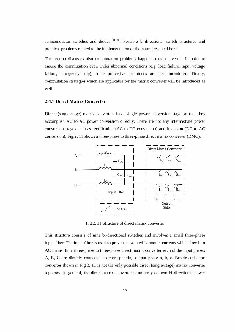
2.4.1 Direct Matrix Converter
Direct (single-stage) matrix converters have single power conversion stage so that they
accomplish AC to AC power conversion directly. There are not any intermediate power
conversion stages such as rectification (AC to DC conversion) and inversion (DC to AC
conversion). Fig.2. 11 shows a three-phase to three-phase direct matrix converter (DMC).
SAa SAcSAb
Output
Side
Input Filter
LA
LB
LC
CAB
CBC CAC
= AC Switch
A
B
C
ba c
SBa SBcSBb
SCa SCcSCb
Direct Matrix Converter
Fig.2. 11 Structure of direct matrix converter
This structure consists of nine bi-directional switches and involves a small three-phase
input filter. The input filter is used to prevent unwanted harmonic currents which flow into
AC mains. In a three-phase to three-phase direct matrix converter each of the input phases
A, B, C are directly connected to corresponding output phase a, b, c. Besides this, the
converter shown in Fig.2. 11 is not the only possible direct (single-stage) matrix converter
topology. In general, the direct matrix converter is an array of mxn bi-directional power
Page 41
18
switches to connect directly m-phases of the voltage source to n-phases of a load [10].
Several studies have been conducted on single-to-single phase and single-to-two phase
matrix converters [11-13]. In the case of direct matrix converters with more than three output
phases, a three-phase to four-phase matrix converter proposed [14] and applied as well [15].
The neutral line here is understood as the fourth output phase. Fig.2. 12 shows such a three-
phase to four-phase matrix converter.
SAa SAcSAb
Output
Side
Input Filter
LA
LB
LC
CAB
CBC CAC
= AC Switch
A
B
C
ba c
SBa SBcSBb
SCa SCcSCb
SAn
SBn
SCn
n
Direct Matrix Converter
Fig.2. 12 Structure of three-phase to four-phase direct matrix converter
A three-phase to three-phase direct matrix converter has higher practical value because it
connects a three-phase voltage supply to a three-phase load, typically a motor.
2.4.2 Indirect Matrix Converter
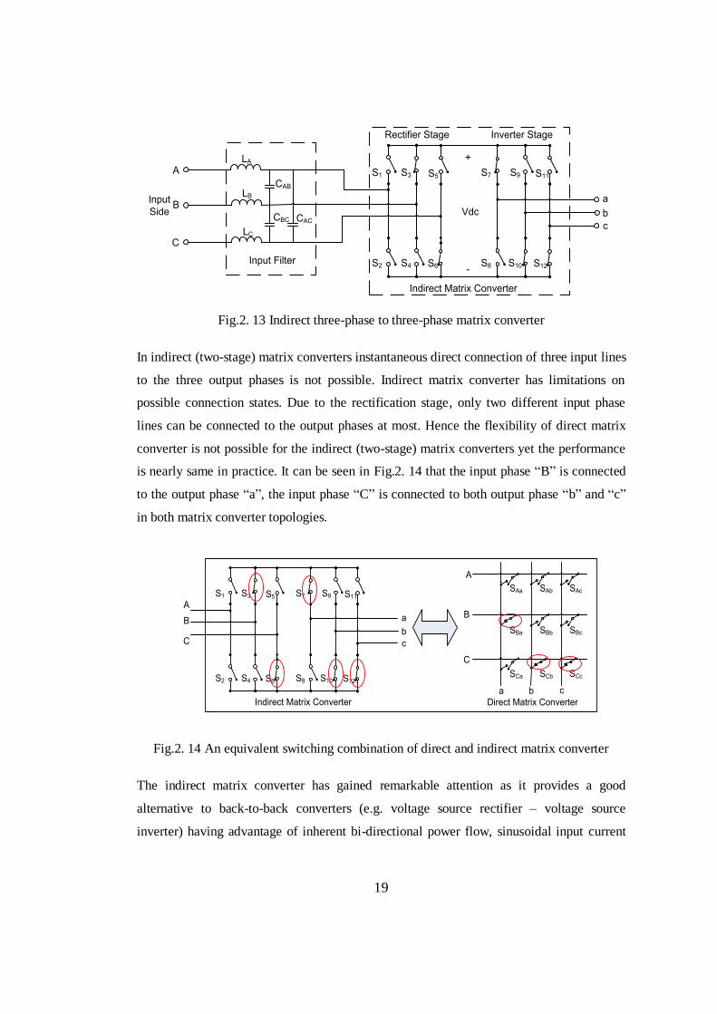
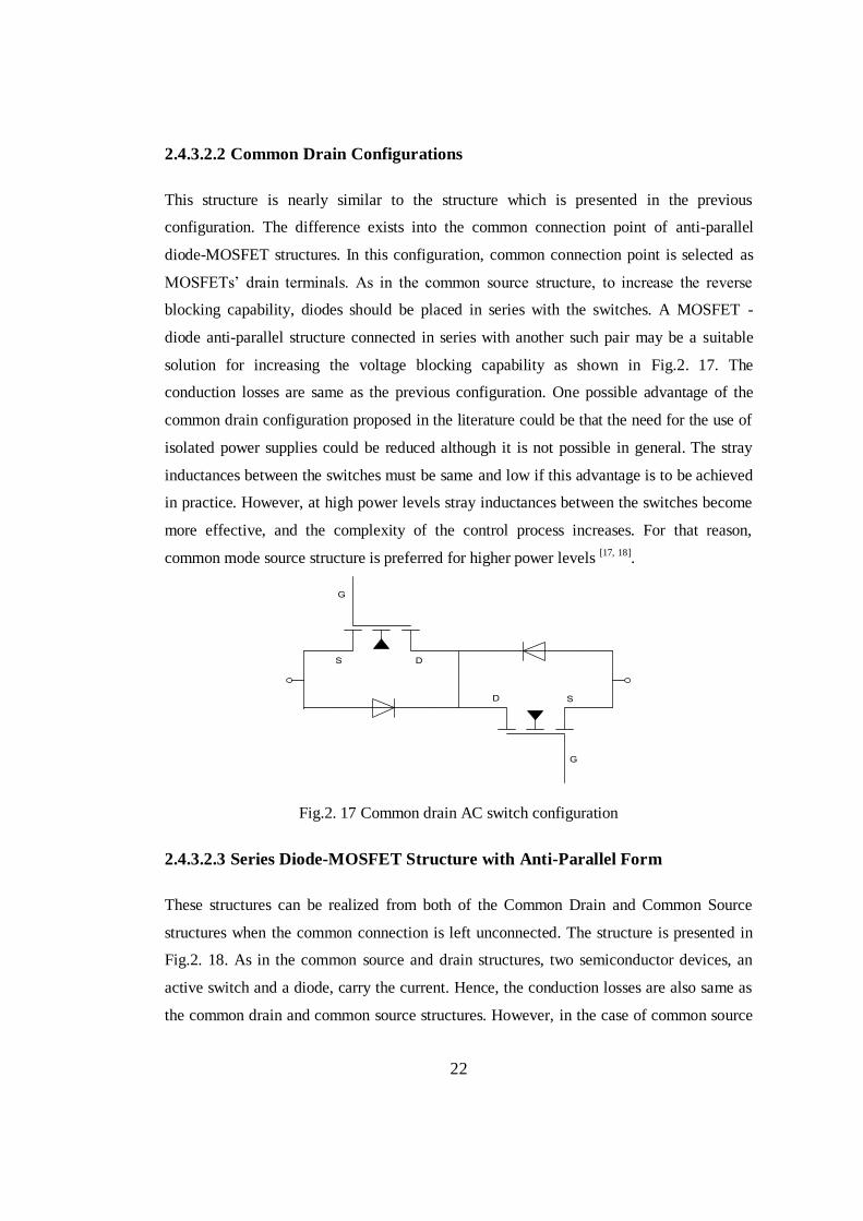
An indirect (two-stage) matrix converter is made of two back-to-back converters without a
DC-link capacitor in between as shown in Fig.2. 13. One of them is a rectifier and other is
the inverter stage.
Page 42
19
a
c
S6
S3
S4
S1
S2
S5
Indirect Matrix Converter
S12
S9
S10
S7
S8
S11
b
Rectifier Stage Inverter Stage
Input Filter
LA
LB
LC
CAB
CBC CAC
Input
Side
A
B
C
+
-
Vdc
Fig.2. 13 Indirect three-phase to three-phase matrix converter
In indirect (two-stage) matrix converters instantaneous direct connection of three input lines
to the three output phases is not possible. Indirect matrix converter has limitations on
possible connection states. Due to the rectification stage, only two different input phase
lines can be connected to the output phases at most. Hence the flexibility of direct matrix
converter is not possible for the indirect (two-stage) matrix converters yet the performance
is nearly same in practice. It can be seen in Fig.2. 14 that the input phase “B” is connected
to the output phase “a”, the input phase “C” is connected to both output phase “b” and “c”
in both matrix converter topologies.
A
B
C
a
c
S6
S3
S4
S1
S2
S5
Indirect Matrix Converter
S12
S9
S10
S7
S8
S11
b
SAa SAcSAb
ba c
SBa SBcSBb
SCa SCcSCb
Direct Matrix Converter
A
C
B
Fig.2. 14 An equivalent switching combination of direct and indirect matrix converter
The indirect matrix converter has gained remarkable attention as it provides a good
alternative to back-to-back converters (e.g. voltage source rectifier – voltage source
inverter) having advantage of inherent bi-directional power flow, sinusoidal input current
Page 43
20
waveforms with minimum harmonics and sinusoidal output waveforms, the possibility of
compact design due to the lack of DC-link reactive components and controllable input
power factor independent from the output current phase angle [16].
2.4.3 Bi-directional Switches
A bi-directional switch is used to conduct currents and block voltages in both polarities, the
energy can flow from source to the load and from load to the source depending on control
signal. However, commercially a proper switch is still not available on the market. For this
reason, an alternative AC switch is realized by a combination of conventional unidirectional
devices. That is other fully controllable semiconductor switches and diodes can be used to
construct AC switches. In general, AC switch topologies can be classified into two groups;
diode bridge topology and switching devices with anti-parallel diode topologies [8, 9]. We
can see the advantages and disadvantages of these structures at below.
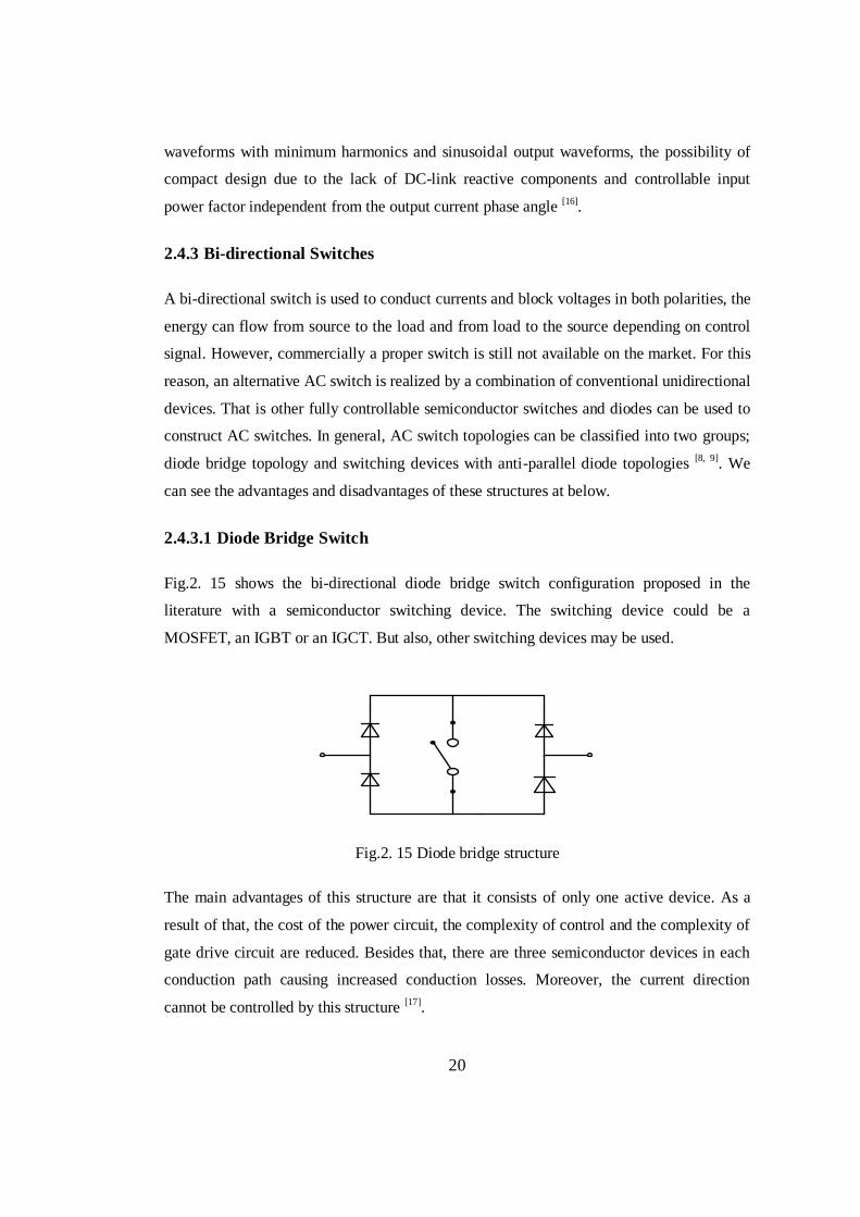
2.4.3.1 Diode Bridge Switch
Fig.2. 15 shows the bi-directional diode bridge switch configuration proposed in the
literature with a semiconductor switching device. The switching device could be a
MOSFET, an IGBT or an IGCT. But also, other switching devices may be used.
Fig.2. 15 Diode bridge structure
The main advantages of this structure are that it consists of only one active device. As a
result of that, the cost of the power circuit, the complexity of control and the complexity of
gate drive circuit are reduced. Besides that, there are three semiconductor devices in each
conduction path causing increased conduction losses. Moreover, the current direction
cannot be controlled by this structure [17].
Page 44
21
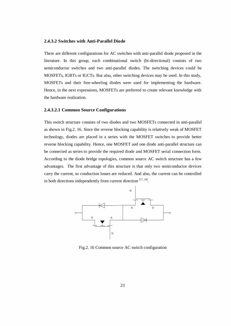
2.4.3.2 Switches with Anti-Parallel Diode
There are different configurations for AC switches with anti-parallel diode proposed in the
literature. In this group, each combinational switch (bi-directional) consists of two
semiconductor switches and two anti-parallel diodes. The switching devices could be
MOSFETs, IGBTs or IGCTs. But also, other switching devices may be used. In this study,
MOSFETs and their free-wheeling diodes were used for implementing the hardware.
Hence, in the next expressions, MOSFETs are preferred to create relevant knowledge with
the hardware realization.
2.4.3.2.1 Common Source Configurations
This switch structure consists of two diodes and two MOSFETs connected in anti-parallel
as shown in Fig.2. 16. Since the reverse blocking capability is relatively weak of MOSFET
technology, diodes are placed in a series with the MOSFET switches to provide better
reverse blocking capability. Hence, one MOSFET and one diode anti-parallel structure can
be connected as series to provide the required diode and MOSFET serial connection form.
According to the diode bridge topologies, common source AC switch structure has a few
advantages. The first advantage of this structure is that only two semiconductor devices
carry the current, so conduction losses are reduced. And also, the current can be controlled
in both directions independently from current direction [17, 18].
D S
G
G
S D
Fig.2. 16 Common source AC switch configuration
Page 45
22
2.4.3.2.2 Common Drain Configurations
This structure is nearly similar to the structure which is presented in the previous
configuration. The difference exists into the common connection point of anti-parallel
diode-MOSFET structures. In this configuration, common connection point is selected as
MOSFETs’ drain terminals. As in the common source structure, to increase the reverse
blocking capability, diodes should be placed in series with the switches. A MOSFET -
diode anti-parallel structure connected in series with another such pair may be a suitable
solution for increasing the voltage blocking capability as shown in Fig.2. 17. The
conduction losses are same as the previous configuration. One possible advantage of the
common drain configuration proposed in the literature could be that the need for the use of
isolated power supplies could be reduced although it is not possible in general. The stray
inductances between the switches must be same and low if this advantage is to be achieved
in practice. However, at high power levels stray inductances between the switches become
more effective, and the complexity of the control process increases. For that reason,
common mode source structure is preferred for higher power levels [17, 18].
D S
G
G
S D
Fig.2. 17 Common drain AC switch configuration
2.4.3.2.3 Series Diode-MOSFET Structure with Anti-Parallel Form
These structures can be realized from both of the Common Drain and Common Source
structures when the common connection is left unconnected. The structure is presented in
Fig.2. 18. As in the common source and drain structures, two semiconductor devices, an
active switch and a diode, carry the current. Hence, the conduction losses are also same as
the common drain and common source structures. However, in the case of common source
Page 46
23
connection left unconnected eighteen isolated supplies are required for the gate drive
control, whereas the common drain structure requires six isolated supplies and common
source structure requires nine isolated supplies for the gate drives of switches. For that
reason, series diode-MOSFET connected anti-parallel form is not commonly used as the
common drain and source structures [17, 18].
D S
G
G
S D
D S
G
G
S D
Fig.2. 18 Anti-parallel series diode-MOSFET configuration
2.4.4 Commutation Problem
In matrix converter topologies, the commutation problem basically caused from the lack of
static freewheeling paths. In practice, purely resistive loads do not exist and therefore the
load current path must always be provided with the active control of semiconductor
switches. Also, the matrix converter commonly works at the switching frequencies from 2
to 10 kHz. Hence, reliable and fast current commutation between AC switches in matrix
converter becomes critical, and safe commutation of the current from one bi-directional
switch to another becomes difficult. Therefore, additional care is to be paid in to the
synchronization of the switching signals [19].
2.4.5 Safe Operation
Likewise the other static converter, the protection issue is also needed for matrix converter
to protect against the overvoltage and the overcurrent due to the restricted capability of
semiconductor switches and diodes. Therefore, an effective protection circuit has an
important role for the reliable operation.
Page 47
24
2.4.5.1 Overvoltage Protection
A voltage surge from the AC mains may cause commutation failure in the converter
operation. To avoid from a possible damage requires the use of some protective schemes in
practice. There are two different protection schemes commonly proposed in the literature.
The first protection scheme uses a clamp circuit to clamp the voltage spikes, the second
uses varistor/suppressor diode protections at the input and output terminals [20].
2.4.5.1.1 Clamp Circuit
The clamp circuit includes a capacitor, two three-phase full-bridge diode rectifier structures
and a discharge resistor as shown in Fig.2. 19. The clamp circuit protects the all nine bi-
directional (18 unidirectional) switches against the surge coming from the utility and the
voltage spikes caused during the emergency shutdown of the converter or a load failure. If
the current flow through the inductive load is interrupted due to an emergency or a load
failure, the stored energy in the load inductance is going to be transferred to the clamp
capacitor. Thus, no overvoltage is going to be produced provided that the clamp capacitor
sufficiently large. Also, output voltage spikes are generated by the parasitic inductances of
power switches and by the timing inaccuracies during the switching task as well. Since the
voltage of clamp capacitor increases at each inaccurate switching operation or voltage surge
coming from the AC mains, a path is needed to discharge the clamp capacitor. Therefore,
although not an efficient solution a resistor is used to discharge the clamp capacitor. This
circuit has the advantage of being very simple. This scheme provides protection for all
operating conditions and has simple hardware requirements. However, it also increases the
number of semiconductor devices and required reactive component. These are the
drawbacks of the clamp circuit protection scheme [21].
Page 48
25
SAa SAcSAb
Output
Side
Input Filter
LA
LB
LC
CAB
CBC CAC
= AC Switch
A
B
C
ba c
SBa SBcSBb
SCa SCcSCb
Cp Rp
Clamp Circuit
Matrix Converter
Fig.2. 19 The use of clamp circuit in direct matrix converter
2.4.5.1.2 Input/Output Varistor/Suppressor Diode Protection
In this strategy, the overvoltage protection is achieved by using varistors or suppressors [22].
This protection scheme is shown in Fig.2. 20. These varistors/suppressors limit the
maximum voltage under overvoltage conditions. This strategy is suitable for low power
ratings. For high power applications, the clamp circuit should be used.
SAa SAcSAb
Output
Side
Input Filter
LA
LB
LC
CAB
CBC CAC
= AC Switch
Input
Side
A
B
C
ba c
SBa SBcSBb
SCa SCcSCb
Protection
Elements
Fig.2. 20 Input/output varistor/suppressor diode protection scheme
Page 49
26
2.4.5.2 Overcurrent Protection
Overcurrent can be a result of a short circuit existing on two (or more) input lines or two (or
more) output phases. In both cases to prevent the damage will be caused from overcurrent,
similar protection strategy can be followed up. Basically, phase currents both of input
phases and output phases are monitored and if any of the phase currents is at above a
predetermined safe value, all semiconductor switches are forced to turn-off. Since the
freewheeling paths are provided with active control of semiconductor switches, at that time
the freewheeling path is destroyed. We know that the freewheeling path is important to
prevent switches from overvoltage spike that will be caused from the inductive load current
interrupt. Therefore, the overcurrent and overvoltage protection strategies must be used
together in matrix converter [19].
2.4.6 Switch Commutation
Based on the discussions given in previous sections, safe current commutation between the
bi-directional switches is more difficult task comparing with the conventional voltage
source inverters and it requires additional attention in timing and synchronization of the
switching signals due to absence of natural freewheeling path. Therefore, active control of
semiconductor switches is always required. Since the matrix converter is supplied by an AC
utility and usually feeds an inductive load, the input lines must not be short circuited and
the output lines must not be open circuited. Considering one output phase of three-phase to
three-phase matrix converter, it is important that two bi-directional switches must not be
switched on at the same time as shown in Fig.2. 21. In this condition, the two bi-directional
switches on output phase “a” are turned - on at the same time. This would result in line-to-
line short circuit and the destruction of the semiconductor switches due to overcurrent.
Page 50
27
SAa SAcSAb
Output
Side
Input Filter
LA
LB
LC
CAB
CBC CAC
= AC Switch
Input
Side
A
B
C
ba c
SBa SBcSBb
SCa SCcSCb
Direct Matrix Converter
Fig.2. 21 Line to line short circuit condition
Moreover, all of the bi-directional switches for any output phase must never be switched -
off at the same time. Otherwise, large overvoltages will result on the switch due to the lack
of a path for inductive load current. Fig.2. 22 represents this situation. In this condition, any
current path does not exist on output phase “c”. This would result high voltage spikes and
the semiconductor switches may be destroyed due to overvoltage.
SAa SAcSAb
Output
Side
Input Filter
LA
LB
LC
CAB
CBC CAC
= AC Switch
Input
Side
A
B
C
ba c
SBa SBcSBb
SCa SCcSCb
Direct Matrix Converter
Fig.2. 22 Output current interrupt
Therefore, to provide safe commutation for matrix converter structures, logical switching
states must be selected. In the literature, many studies were conducted on safe commutation
strategies of matrix converter. Considering the reliability and efficiency, these commutation
strategies can be divided in two different groups. In early implementation of matrix
converters, dead-time and overlap techniques were used. The first group includes these two
techniques. However, these techniques produce overcurrent and voltage spikes. Hence, they
Page 51
28
are not so safe and require additional elements like as snubbers, clamping circuit and
additional line inductors. Later, multi step commutation methods were implemented in the
literature. The multi step commutation methods have been named as “Output Current
Direction Based Commutation”, “Input Voltage Polarity Based Commutation” and “Mixed
Commutation Method” which is a combination of both “Output Current Direction Based
Commutation” and “Input Voltage Polarity Based Commutation” methods. The basic idea
in these methods is to perform the required switch commutations by complying with the
basic matrix converter rules. The first commutation method is based on the output current
direction information, the second method is required to sense the input voltage polarities
and the last one needs the both information.
In the literature, two and four step commutation strategies are generally evaluated to
perform current direction based and input voltage polarity based commutation methods.
The four-step current commutation technique was proposed in the literature [9], and it did
not require any snubbing or limiting elements. Besides this, other current based
commutation methods which require two steps are proposed in [23-24] in the literature.
Moreover, another idea which uses input voltage magnitude was introduced in [25]. The
purpose of this proposed input voltage magnitude based modulation techniques is to
eliminate the complexity of control and reduce the number of steps used at the
commutation instant. This technique exactly requires two steps for the bi-directional switch
commutation. And it is also named as two-step voltage polarity based commutation
method. Also, four-step commutation based on input voltage polarity has also been
implemented [26]. However, both of the current direction based and voltage polarity based
commutation techniques rely on the accurate measurement of current polarity or voltage
polarity, otherwise these may lead to commutation failure. Therefore, new modulation
technique has been introduced [27] to increase the reliability of these commutation
techniques. In this technique, both the input voltage and the output current polarities feed
the control structure to perform the commutation process.
In this section, current direction based commutation method is explained first. Then, the
voltage polarity based commutation methods are mentioned. After the explanation of
current direction based and voltage polarity based modulation techniques, the mixed
commutation technique is introduced.
Page 52
29
2.4.6.1 Output Current Direction Based Commutation Methods
In this section output current direction based commutation strategies are introduced.
2.4.6.1.1 Four-Step Commutation Strategy Based on Current Direction
The main idea of the safe commutation is to eliminate the switch state combinations which
lead to the short circuit between input lines and open circuit at output phases. Before
explaining the principle of the current direction based four-step commutation strategy, one
output phase of three-phase to three-phase direct matrix converter is presented in the Fig.2.
23 to provide better understanding on switch commutations.
GAa2
GAa1
S
D
D
GBa2
GBa1
S
D
D
GCa2
GCa1
S
D
DAa1
Aa2
DAa2
DAa1
Ba1
Ba2
DBa2
DBa1
Ca1
Ca2
DCa2
DCa1
Output Phase a
A B C
Three Phase Inputs
Leg1
Leg2
Leg3
Fig.2. 23 One output phase structure of direct matrix converter
Each leg involves two common source connected N-channel MOSFETs and two anti-
parallel diodes. The bi-directional switches formed in common source configuration. The
switch state of these MOSFETs have very important role for safe commutation. Firstly,
consider only the Leg1 of the output phase “a” of the direct matrix converter structure to
simplify the role of switches on the commutation strategy. The allowable current flow
directions are shown in Table 2. 1 according to the switch state combinations. The
remaining legs may also be considered in the same manner.
Page 53
30
Table 2. 1 The allowable current directions according to the switch state combinations
Description Switch States Input
Phase Current
Direction Output Phase Aa1 Aa2
Current cannot flow in
both direction Open Open A
a
Current can flow in one direction
Open Close A
a
Current can flow in one direction only
Close Open A
a
Current can flow in both directions
Close Close A
a
The “Current Direction” arrows in the Table 2. 1, show directions of the current flow
between the “Input Phase, A and Output Phase, a” columns. When a commutation from a
bi-directional switch to another bi-directional switch is to take place, the current direction
plays an important role to select steps of switch commutation. The following explanation
assumes that the load current is in the direction of arrows (e.g from input phase to output
phase) shown in Fig.2. 24 and initially the switches, in the Leg1, are turned-on.
GAa2
GAa1
S
D
D
GBa2
GBa1
S
D
D
GCa2
GCa1
S
D
DAa1
Aa2
DAa2
DAa1
Ba1
Ba2
DBa2
DBa1
Ca1
Ca2
DCa2
DCa1
Output Phase a
Leg1
Leg2
Leg3
A B C
Three Phase Inputs
ia
iAa
Fig.2. 24 One output phase structure
Page 54
31
At a time instant, the commutation of the ia current from input phase “A” to input phase
“B” is required. Since the semiconductor switches have different turn - on / turn - off times
and propagation delays, simultaneous turn - off of the switches in Leg1 and turn - on of the
switches in Leg2 are not possible. Therefore, after switching-off the switches in Leg1, a
dead-time should be introduced to ensure that they are turned - off before the turning - on of
the switches in Leg2. However, this time, the inductive output current is interrupted and a
voltage spike is induced on opened switches. From the above discussions it is clear that this
basic strategy is also harmful. Since this transition cannot be made by using this strategy, a
logical switching sequence should be selected during the commutation of the output phases
between two input lines. The solution of this problem requires particular care to be paid in
the timing and synchronization of the switching signals using only appropriate switch state
combinations according to the current direction [28].
In order to prevent the voltage spike, the inductive load current which is drawn from the
output phase “a” should be able to continue without any interruption when both
unidirectional switches in Leg1 are turned-off. Therefore, the inductive current should have
a current path to flow in Leg2, as shown in Fig.2. 25.
GAa2
GAa1
S
D
D
GBa2
GBa1
S
D
D
GCa2
GCa1
S
D
DAa1
Aa2
DAa2
DAa1
Ba1
Ba2
DBa2
DBa1
Ca1
Ca2
DCa2
DCa1
A B C
Output Phase a
Leg1
Leg2
Leg3
ia
Three Phase Inputs
Fig.2. 25 Freewheeling current path in Leg2
Page 55
32
Basically, the current paths in Leg1 and Leg2 which allow current to flow in the direction
of ia current can be provided in four different combinations. However, one of these
combinations is nonhazardous. Now, consider the switch state combinations one by one.
First Combination
All switches in Leg1 and Leg2 are turned-on. Referring to Table 2. 1, the switch state
allows bi-directional power flow and a path for the current flow is established. However,
this leads to the short circuit of input phase lines.
Second Combination
All switches in Leg1 and only upper switch (Ba1) of Leg2 are turned-on. Referring to Table
2. 1, the switch state allows bi-directional power flow in Leg1 and a unidirectional power
flow in Leg2. A current flow path is again established. However, this leads to the short
circuiting of input lines if input voltage of phase “B” is greater than the input voltage of
phase “A”. The short circuit current flows from input phase “B” to the input phase “A”.
Third Combination
All switches in Leg2 and only upper switch of Leg1 (Aa1) are turned-on. Referring to
Table 2. 1, the switch state allows bidirectional power flow in Leg2 and a unidirectional
power flow in Leg1 thus establishing a path for the current flow. However, this connection
scheme also leads to be short circuiting of input phase lines if the input voltage of phase
“A” is greater than the input voltage of phase “B”.
Fourth Combination
Only upper switches in Leg1 (Aa1) and Leg2 (Aa2) are turned-on. As displayed in Table 2.
1, the switch state allows only a unidirectional power flow in both, Leg1 and Leg2. There is
no risk of short circuiting of input lines in this connection scheme.
There are two restrictions for the safe commutation of matrix converter as mentioned previous parts.
While providing a path for the current of an inductive load, input lines must not be
short circuited.
While changing the switch states, the current of the inductive load should not be
interrupted.
Page 56
33
By considering these two limitations, only the fourth combination is appropriate condition
to eliminate these dangerous situations. Similarly, all appropriate switch state (S : switch
state) combinations can be given by considering the output current directions.
Table 2. 2, displays all switching combinations for four-step current direction based
commutation strategy as a summary.
Table 2. 2 All switching combinations for current based commutation
S MOSFET Switches
Aa1 Aa2 Ba1 Ba2 Ca1 Ca2
Ia
Direction
1 close close open open open open +,-
2 open open close close open open +,-
3 open open open open close close +,-
4 close open open open open open +
5 open close open open open open -
6 open open close open open open +
7 open open open close open open -
8 open open open open close open +
9 open open open open open close -
10 close open close open open open +
11 open close open close open open -
12 open open close open close open +
13 open open open close open close -
14 close open open open close open +
15 open close open open open close -
In accordance with the above explanations, a commutation is required from S = 1 to S = 2
(Leg1 to Leg2) with the direction of inductive load current being positive. Positive current
direction means that current flows from input to output. Then, interim steps should only
cover the switch states which affect the current commutation in the Leg1 and Leg2. As a
result, fourth, sixth and tenth switch states can be used as interim steps considering the
current direction so that the switching sequence should be the following:
I. Turning-off Aa2 (S = 4)
II. Turning-on Ba1 (S = 10) III. Turning-off Aa1 (S = 6)
Page 57
34
IV. Turning-on Ba1 (S = 2).
Also, a dead-time should be introduced between interim steps. Hence, the gate control
signals should be applied according to sequence which is shown above. Fig.2. 26 presents
the timing diagram of gate control signals.
t1 t2 t3 t4 t
0
0
0
0
1
1
1
1
GAa1
GAa2
GBa1
GBa2
Dead-time
Fig.2. 26 Control signals of unidirectional switches
2.4.6.1.2 Two Step Commutation Strategy Based on the Current Direction
The main idea of this strategy is to keep the non-conducting switches turned - off during the
commutation process including the non-conducting switch on active bi-directional switch.
The two-step commutation strategy was proposed in [28]. When a commutation is required
to a different leg, only the switch which is required to generate the path for inductive load
current in the sensed direction will be turned - on. After the creation of the new current
path, first activated switch is turned - off by the second step. This method is effectively
used when the output current is absolutely higher than a small predefined positive threshold
value. If the absolute output current level drops down to a smaller level than the threshold
value, the sense of the output current direction becomes unreliable and this situation makes
that two-step method is much complicated [28].
Fig.2. 27 reflects this strategy. If the current, ia is higher than the threshold, only the upper
switch (Aa1) is turned-on.
Page 58
35
GAa2
GAa1
S
D
D
GBa2
GBa1
S
D
D
GCa2
GCa1
S
D
DAa1
Aa2
DAa2
DAa1
Ba1
Ba2
DBa2
DBa1
Ca1
Ca2
DCa2
DCa1
A B C
Output Phase a
Leg1
Leg2
Leg3
ia
Three Phase Inputs
Fig.2. 27 Inductive current path in two step commutation
However, if the current is smaller than the threshold, the use of the on switch only will
cause the current interrupt due to change of the current direction or wrong current direction
detection. Therefore, both switches on a leg should be turned-on for low current levels to
allow a change in the current direction. The commutation type occurring at the instant of
the current direction change in the same current path (in a leg) is called as “Inter Switches
Commutation”. To provide the reverse current path, both switches (Aa1 and Aa2) must be
turned-on as shown in Fig.2. 28.
Inter-Switches
Commutation
0
Negative
Treshold
Value
Positive
Treshold
Value Positive Current
Direction
Negative Current
Direction
Current in positive
direction
Aa1 = ON
Aa2 = OFF
Aa1 = OFF
Aa2 = ON
Aa1 = ON
Aa2 = ONia
iAa
Fig.2. 28 Inter-Switches Commutation
Page 59
36
When a commutation between different phases (e.g. between two input lines) is required,
the “Inter Switches Commutation” should be disabled to avoid line-to-line short-circuit.
This can be realized in two different ways. The first one is based on disabling the current
commutation between different input lines until the current level abandons the threshold
value. In other words, the last switch state will not be changed until the current reach
threshold value. After that value, the output current direction will be sensed correctly. Then
switch states can be reliably selected. This method is known as “two-steps commutation
with threshold”. However, this compulsory time interval can affect the quality of the output
current waveforms seriously because of in this time interval, the output current cannot
reverse direction. That means, if the turned-on unidirectional switch is not an appropriate
switch state, the current level rises in the opposite direction. In the second way, if the
commutation is to happen between different input lines and the current is close to the
threshold or within threshold value, a dead-time can be used between the switch
commutations. Firstly turned-on switch is opened and after the dead-time duration, the new
unidirectional switch in other leg is turned-on. During this time interval, the current
commutation is interrupted. This commutation process is known as two-step commutation
with dead-time in threshold. The switch commutation interval is half of that resulting in
four-step commutation strategies. Hence, faster commutation process can be possible.
However, the two-step method is much complicated [28] and causes the disruptive effects on
output current as mentioned above.
2.4.6.2 Input Voltage Polarity Based Commutation Methods
In the previous section output current direction based commutation methods have been
investigated. In this section, commutation techniques depending on the input voltage
polarity information have been introduced.
2.4.6.2.1 Four-Step Commutation Strategy Based On the Input Voltage
Polarity
The basic idea in this strategy is to provide the same operating conditions of a commutation
process as in a traditional DC-link inverter. In order to establish the same operating
conditions, the input phase voltages have to be known in real time. While the output phase
Page 60
37
is remaining connected to an input line, both switches which are used for constructing the
bi-directional switch are turned - on. Besides when a commutation of output phase between
different input lines is to happen, real time input line voltages must be known so that we
can decide whether upper or lower switch should be turned - on (assume commutation is to
happen between Input Phase “A” and Input Phase “B” and also > ) in the newly
current commutation required leg. After this process a freewheeling path should be
established in between the new input line and output line by turning-on MOSFET Ba2. The
remaining semiconductor switch (Ba1) prevents the short circuit between the input lines.
Then the other freewheeling path can be formed by turning - off one of the switches in
firstly current commutated leg (Leg1). Fig.2. 29 illustrates this strategy.
Freewheeling
Diode
Freewheeling
Diode
Allowed
current flow
direction
Allowed
current flow
direction
ia
Fig.2. 29 Allowed current directions ( > )
The freewheeling paths allow the current flows in both directions. The active switch in
Leg1provides a path for the current flow from input phase to output phase and the active
switch in Leg2 provides the current flow in the opposite direction. The switching sequences
with possible input voltage polarities are introduced as follow:
If the input phase A voltage level is lower than the input phase B voltage level:
I. Turning-on Ba2
II. Turning-off Aa2
Page 61
38
III. Turning-on Ba1 IV. Turning-off Aa1
If the input phase A voltage level is higher than the input phase B voltage level:
I. Turning-on Ba1
II. Turning-off Aa1
III. Turning-on Ba2
IV. Turning-off Aa2
Since the turn - on and turn - off delays of semiconductor switches are different, in order to
avoid from a probable short circuit between the input lines a blanking time should be
inserted between the steps. In this commutation strategy, any hazard of open-circuiting the
current flow path is completely removed due to freewheeling paths provided in both
directions. However, it is not true for the hazard of the short circuiting. In other words, near
the crossing points of input voltages (e.g. critical regions for voltage based strategies), the
input voltage polarity may have not been sensed correctly. As a result of this situation a
short circuit path may be established. Therefore, a reliable measurement of input line
voltages is required [26].
2.4.6.2.2 Two-Step Commutation Strategy Based On the Input Voltage Polarity
In this section, a two-step commutation strategy is investigated. The commutation strategy
is also called Metzi commutation and proposed in [29]. The basic principle of this strategy is
based on the operating condition which establishes freewheeling paths for both output
current polarities at any time. Since the switching sequences are determined using the
information of input line voltages, the Metzi strategy also requires reliable measurement of
input line voltages near the crossing points presented as in Fig.2. 30.
Page 62
39
Fig.2. 30 Critical and uncritical intervals for detecting of input voltage polarities
The area in the red dashed rectangle is demonstrated the uncritical region. The potential
difference between the input line voltages is high in this interval. Hence, the possibility of
wrong detection of input voltage polarities is really low. However, it is not true for the area
in the black dashed rectangle which demonstrates the critical region of commutation
process. There are a few ways to manage a commutation required within this interval. The
first is based on disabling (postponing the request) the commutation until the potential
difference abandons the critical region and this is called as “Prohibition”. However, the
connection time of the output phase to input phases should be recalculated considering this
fact in this time interval. Actually, in this time interval the input line voltage levels are
nearly equal. Therefore, this situation does not affect the output voltage and current
waveforms. But, it will distort the input currents. A second way called as “Replacement” is
to change the switching sequence by adding uncritical commutations. However, this
strategy increases the converter switching losses and commutation time due to the
additional commutations in this interval. These are the disadvantages of this strategy [30].
2.4.6.3 Multi-Step Commutation Strategy Based On Output Current and Input
Voltage Polarity
In the previous sections, commutation methods based on the output current direction and
the input voltage polarity have been introduced. This section introduces another
commutation strategy based on both output current direction and input voltage polarity.
Fig.2. 31 shows the principle of this hybrid commutation method.
Critical
Region
Uncritical
Region
VA VB VC
Page 63
40
VA VB VC
Output Phase
Current
Input Phase
Voltages
Critical region for
current based
commutation
Critical region for current
based commutation Critical region for
current based
commutation
Critical region for
voltage based
commutation
Fig.2. 31 Critical and uncritical intervals for output current direction and input voltage polarity based commutations
One of the former commutation methods based on the output current direction may cause
an open-circuit in the current path if the load current is around zero, and the other
commutation method based on the input voltage polarity may lead a line-to-line short
circuit for a voltage difference of around zero. The proposed method combines both
commutation methods based on current and voltage as follows [29]:
At the zero crossing point of the load current, voltage based commutation method
is used.
At the zero crossing point of the voltage difference, current based commutation
method is used.
Thus, this mixed method can decrease possibility of the commutation failure without the
need for a high accuracy detection circuit. There are two types of these hybrid commutation
methods used in practice; one that mostly uses the current based commutation method, and
the other that mostly uses the voltage based commutation method. When the output phase
current frequency is lower than the input voltage frequency, current based commutation
technique will be preferred. Because, the selection process, whether the current based
commutation method or voltage based commutation method should be used, decreases.
Page 64
41
Hence, for the lower output current frequencies current based commutation technique is
suitable. Besides that, if the output current frequency is higher than the input voltage
frequency, opposite case is suitable [27].
Page 65
42
CHAPTER 3
PERMANENT MAGNET SYNCHRONOUS MACHINES
The permanent magnet synchronous machine has permanent magnets instead of field
windings. The permanent magnet synchronous machines can be classified into two main
groups according to the installation of the permanent magnet materials on the rotor, Surface
Mounted Permanent Magnet (SMPM) machines and Interior Permanent Magnet (IPM)
machines. The magnets can be mounted on the rotor surface or they can be internal to the
rotor. The permanent magnets are located on the outer surface of the rotor core in surface
mounted permanent magnet machines, as shown in Fig.3. 1 [31].
Permanent magnet
material
Magnetic
material
d-axis
q-axis
Fig.3. 1 Permanent magnet rotor construction using surface mounted magnets
In interior permanent magnet machines, the permanent magnets are embedded inside the
rotor core. The structure of the interior permanent magnet machine is given in Fig.3. 2.
Page 66
43
Permanent magnet
material
Magnetic
material
d-axisq-axis
Flux barrier
Fig.3. 2 Permanent magnet rotor construction using embedded magnets
The rotor magnetic axis is called direct axis (d-axis) or field flux axis and the principal path
of the flux is trough the magnets. The torque axis (quadrature axis or q-axis) of rotor is
electrically orthogonal to the direct axis. Regardless of the manner of mounting the
permanent magnets on the rotor, the basic principle of operation of machines are same. An
important difference exists between the direct and quadrature axes inductances for different
types of permanent magnet synchronous machines. The SMPM machines have many small
permanent magnet materials that are placed whole surface of the rotor. Therefore, they have
symmetrical reluctance in both axes and they are non-salient pole synchronous machines. In
other words, the d and q axes reactances of SMPM machines are equal ( ). The
arrangement of the permanent magnets to the rotor surface provides the highest air gap flux
density as is directly faces the air gap without the interruption of any other medium such as
part of rotor laminations. Drawbacks of such an arrangement are; lower structural integrity
and lower mechanical robustness. Besides that, the interior construction relieves the
problem of retaining the magnets against centrifugal force. Therefore the interior
construction is suitable for high-speed applications [31].
3.1 STEADY-STATE MODELING OF SMPM SYNCHRONOUS
MACHINE
This section presents steady-state analysis of the surface mounted synchronous machines
considering the per-phase steady-state equivalent circuit shown as in Fig.3. 3 [32].
Page 67
44
Ẽa
Ra jXs
+
-
Ṽa
+
-
Ĩa
Fig.3. 3 Per-phase equivalent circuit of non-salient surface mounted permanent magnet synchronous machine
In Fig.3. 3, is the motor terminal voltage, is the back-emf voltage induced due to the
permanent magnet flux and is the motor phase current. And Ra and Xs are the per-phase
winding resistance and synchronous reactance. From the equivalent circuit, we can write
(3-1)
The average power input to the machine;
(3-2)
where is the power-factor angle between the applied voltage and the phase current. and
are the rms values of phase voltage and current.
The total copper (electrical) loss in a surface mounted permanent magnet synchronous
machine is;
(3-3)
By subtracting the total copper loss from the power input, we obtain the power developed
by a surface mounted permanent magnet synchronous machine as;
(3-4)
Eddy current and hysteresis losses are also assumed as negligible.
Steady-state phasor diagram for the SMPM machine by neglecting the winding resistor is
given in Fig.3. 4.
Page 68
45
d
Ṽa
Ẽa
jXs Ĩa
Ĩa
ɸ
Fig.3. 4 Phasor diagram of the non-salient SMPM machine
From the per-phase equivalent circuit in Fig.3. 3, the total output power can be written as
[32];
(3-5)
For the flux linkage f due the permanent magnets and the electrical speed , the back-
emf is given by;
(3-6)
If is the angular velocity (rad/s) of the motor, the electromagnetic torque developed by
the motor is then given as;
(3-7)
and we are related by;
(3-8)
where is the pole number.
Then, from (3-6) – (3-8) the electromagnetic torque equation can be obtained as;
(3-9)
Page 69
46
It is obvious that the maximum torque can be achieved by controlling the magnitude and
phase of the phase current .
3.2 DYNAMIC MODELING OF THE SMPM SYNCHRONOUS MACHINE
In the previous section, steady-state analysis of the surface mounted permanent magnet
synchronous machines was introduced. This section presents the dynamic model of
permanent magnet synchronous machine. The mathematical model of permanent magnet
synchronous machine is developed with the help of Park and Clarke transformations which
are derived in Appendix A. Actually; the model of permanent magnet synchronous machine
is nonlinear. For simplicity, the following assumptions are made in the derivation:
Saturation in machine is neglected,
The back-emf is purely sinusoidal,
Eddy currents and hysteresis losses are negligible,
Balanced three-phase voltage source is considered.
There is no external voltage supply connected to the rotor side and the permanent magnet
flux variation is negligible. Therefore, rotor voltage equations need not to be taken into
account in the SMPM synchronous machine modeling [33].
The circuit equations of the three stator windings in terms of phase variables can be written
as:
(3-10)
where Ra, Rb, and Rc are the stator resistances, La, Lb, Lc the self inductances, and Lab, Lba,
Lca, Lac, Lbc, Lcb the mutual inductances. Assume that the stator windings are balanced and
there is no change in the rotor reluctance with rotor position change for surface mounted
permanent magnet synchronous machines, then
(3-11)
Page 70
47
(3-12)
where and we have that;
(3-13)
In Fig.3. 5, a dynamic phase equivalent circuit of SMPM is presented.
ea
Rs L-M
>ia
+
-
va
+
-
Fig.3. 5 Phase equivalent circuit of a SMPM
A two-phase equivalent equations and d-q model of a permanent magnet synchronous
machine rotating at the synchronous speed is obtained by using Park and Clarke
transformations which are given in Appendix A.
(3-14)
(3-15)
(3-16)
Fig.3. 6(a) and Fig.3. 6(b) show the dynamic two-phase equivalent circuit.
Page 71
48
wef
Rs
>iq
+
-
vq
+
-
Lq
Ldweid
+ -
Lqweiq
Rs
>id
+
-
vd
+
-
Ld
(a) (b)
Fig.3. 6 Two-phase (d, q) equivalent model of SMPM synchronous machine
For three-phase permanent magnet synchronous machines, the input power (pin) can be
represented as:
(3-17)
which in terms of d, q variables is;
. (3-18)
The output power, can be obtained from the (3-18) by ignoring the copper losses.
(3-19)
where,
(3-20)
.
(3-21)
The instantaneous torque T is obtained by dividing the output power, by mechanical
speed .
(3-22)
The torque equation includes two terms. First term is called as “the mutual reaction torque”
that is produced from the interaction between the permanent magnet flux, and current
component. The second term corresponds to the “reluctance torque” due to the differences
between d-axis and q-axis reluctances. In order to produce additive reluctance torque,
Page 72
49
must be negative and must be greater than . Besides that, the reluctance variation
between the direct (d-axis) and quadrature (q-axis) axes is fairly small in non-salient
surface mounted permanent magnet synchronous machine. Therefore, the second term,
“reluctance torque”, can be neglected for this machine type [33]. The output torque (T) is
linearly dependent with the magnet flux and q-axis current;
.
(3-23)
Page 73
50
CHAPTER 4
OPERATIONAL ISSUES OF MATRIX CONVERTER
In this chapter, the modulation strategies for matrix converter are introduced. First, a state-
space model of matrix converter is presented to provide basic background on input/output
characteristics. That is followed by a review of matrix converter modulation methods
presented in the literature. Then, space vector definition is described. Finally, the
derivations of the space vector pulse width modulation (SVPWM) methods for matrix
converter topologies are presented.
4.1 STATE-SPACE MODEL OF MATRIX CONVERTER
A simplified three-phase to three-phase direct matrix converter model is shown in Fig.4. 1.
This model consists of nine ideal AC (bi-directional) semiconductor switches which allow
each of the three output lines to be connected to any of the three input lines. In this
topology, a three-phase output voltage with adjustable magnitude and frequency is directly
synthesized from three-phase AC mains.
Page 74
51
VA
VB
VC
SAa SAcSAb
SBa SBcSBb
SCa SCcSCb
Three Phase
Balanced Load
Pha
se a
Pha
se b
Pha
se c
i a i b i c
Three Phase
Power Supply
Output
Side
Input
Side
i C
i B
i A
Fig.4. 1 Simplified three-phase to three-phase matrix converter
There is another matrix converter topology with no DC-link capacitor, known as indirect
matrix converter as mentioned in Section 2.4.2. In indirect matrix converter topology, the
three-phase AC mains voltage is first converted into a fictitious DC-link voltage. Then, the
fictitious DC-link voltage is inverted in to the required AC output voltages. Besides these
differences, the input–output voltages and currents show similar characteristics. The
instantaneous input phase voltages and currents are given by the following equations;
. (4-1)
Then, the instantaneous input line-to-line voltages can be written as,
(4-2)
where is the peak value of the input line-to-line voltages and is the input angular
frequency.
Page 75
52
The input line currents are given as;
(4-3)
where is the peak value of three-phase input currents. The input currents have a phase
angle with respect to the input phase voltages. This angle can be set to zero to obtain
unity power factor control. The output phase voltages and currents are given by;
, (4-4)
. (4-5)
where is the peak value of ouput voltages, is the peak value of the output currents,
is the output angular frequency and is the phase difference between the output voltages
and currents.
Then, the instantaneous input and output voltages are related by;
(4-6)
and the instantaneous input and output currents are related as;
. (4-7)
The switching function in (4-6) – (4-7) denotes the instantaneous states of AC switches
and it is either “0” when the switch is “off” or “1” when the switch is “on”. Note that Y ϵ
{ A, B, C} and x ϵ { a, b, c}.
Page 76
53
Since in the matrix converter only one AC switch must be closed on each output phase at
any time this prevents the line-to-line short circuit of the input supply. Moreover, all AC
switches in an output phase must not be opened at the same time to avoid the open circuit at
the load sides because any natural freewheeling path exists for the inductive load current.
These constraints can be stated formally by;
(4-8)
4.2 VOLTAGE AND CURRENT WAVEFORMS GENERATION IN
MATRIX CONVERTERS
In principle, the aims of the modulation methods to synthesize the voltage and current
waveforms are identical. All modulation methods are used to create target waveforms at the
converter input and output terminals. Actually, these modulation methods show difference
in quality of the generated input and output waveforms. Considering this fact, the ideal
modulation methods to generate the input-output current and voltage waveforms of matrix
converter should provide the following specifications [34]:
Independent control of frequency and magnitude of the generated output voltages,
Sinusoidal input currents with full control of power factor,
Maximum input voltage to output voltage transfer ratio,
Minimum low order harmonics, low total harmonic distortion and minimum
switching losses,
Efficient implementation.
The matrix converter control strategies were first mentioned by Alesina and Venturini. The
first modulation method for current and voltage waveforms generated by matrix converters
were proposed in 1980, by Venturini [35]. This is the first modulation method proposed for
the generation of input-output waveforms of matrix converter. However, the first method
has the drawback of low input voltage to output voltage transfer ratio as 0.5.
In 1985 a control technique based on a different approach was proposed [2,36]. Input voltages
are first rectified to generate an imaginary DC-link voltage, later the DC-link voltage is
Page 77
54
inverted to generate desired output voltages. This approach provides higher voltage transfer
ratio of 0.86. However, it still had limitation in the input power factor control.
In 1988, Alesina and Venturini proposed a new PWM modulation method to generate
input-output waveforms of matrix converter [37]. This method also eliminates the drawback
of first modulation method of Venturini and known as Venturini’s Optimal Method. By this
method, the voltage transfer ratio is increased at a maximum value of 0.86.
In 1989 Roy and April proposed a scalar PWM method as an alternative method for matrix
converter input-output waveforms generation [38].
The space vector pulse width modulation method for matrix converter was first mentioned
in [39] in 1989. The first SVPWM method had also two distinct control stages. Those are a
rectification stage which provides a constant fictitious DC voltage and an inverter stage
which generates the three-phase target voltage waveforms. This modulation method is
named as indirect or two-stage SVPWM in the literature. By this method, control of input
power factor is not possible. An advanced space vector PWM method was proposed in
1991 which allowed to the control of the input power factor [5].
In 1993 Casadei, Grandi, Serra and Tani proposed a space vector PWM method in [40]. It
does not involve any rectification and inversion process. The power was converted directly
from an AC form to another AC form by this method.
The matrix converter PWM methods described in the literature can be classified into two
categories, the direct PWM approach and the indirect PWM approach.
The Alesina and Venturini method, single-stage or direct space vector PWM and scalar
PWM methods are examples of direct PWM approaches.
The two-stage or indirect space vector PWM methods are classified in indirect PWM
approach in the literature.
The indirect matrix converter topology can be fully matched the physical implementation of
the indirect space vector PWM method [41]. As mentioned in Section 2.4.2, the indirect
matrix converter topology consists of a rectifier stage at the input side and a conventional
voltage source inverter (VSI) at the output side. These two stages are fictitious rectification
and fictitious inversion stage. Modulation methods of rectifier and inverter stages can be
analyzed separately for simplification.
Page 78
55
4.2.1 Matrix Converter Modulation Methods of Alesina and Venturini
By the first modulation methods of Venturini, reachable maximum input to output voltage
transfer ratio is 0.5 because fundamental voltage waveform is always between the negative
and positive envelope of the input voltage waveforms [4]. The method uses a switching
frequency much higher than both frequencies at the input and at the output. The aim in
using the Alesina and Venturini PWM method is to find a modulation matrix M(t) which
satisfies [42];
, (4-9)
, (4-10)
where the modulation matrix M(t) defined above has the following matrix form;
. (4-11)
Due to the use of high switching frequency the desired output voltage waveforms can be
can be constructed from the input voltage waveforms. This also allows constructing the
desired input currents from the output currents.
By considering (4-8), a typical switching pattern for the matrix converter can be illustrated
as in the Fig.4. 2. For the following illustration, it is assumed that the switches can change
their states instantaneously at the switching instant.
Page 79
56
SAa = 1
SAb = 1
SAc = 1
SCa = 1SBa = 1
SBb = 1 SCb = 1
SBc = 1 SCc = 1
Ts
tAa tCatBa
tAb tCbtBb
tAc tCctBc
Fig.4. 2 A possible switching pattern
“Ts” represents the switching period or complete PWM cycle and represents the on
period of the corresponding switches, where
. Then, the modulation duty-ratio (i.e. duty ratio of switch ) can be
defined as
(4-12)
with , where Y ϵ { A, B, C} and x ϵ { a, b, c}.
The construction of PWM waveforms based on proposed method by Venturini and Alesina
is based on the direct calculation of the modulation matrix [35];
(4-13)
where
(4-14)
Page 80
57
(4-15)
where and are the output and input angular frequencies,
,
,
,
,
(4-16)
with the following restrictions;
.
The maximum value of input to output voltage transfer ratio, q is 0.5. This is the drawback
of this modulation technique.
In 1988 Venturini and Alesina proposed an improved PWM technique applicable to the
matrix converters which increased the maximum input voltage to output voltage transfer
ratio to 0.86. The idea was based on the injection of third order harmonic component of
input and output voltages to the output reference voltage. When the magnitudes of those
third-order components were chosen correctly, the voltage transfer ratio could be raised to
0.86. As a result of that, matrix converter output voltages can be defined as follows [6]:
(4-17)
Page 81
58
The entries in the PWM matrix, M(t) of improved solution can be described as follows [6]:
Note that the subscript 6 in (4-18) indicating that the argument in brackets is to be
computed modulo 6.
(4-18)
where k, h ϵ { 1, 2, 3} and
.
Also the entries (e.g. ) of PWM matrix, M(t) have the following relation:
4.2.2 Space Vector
Assume , and are magnitudes of three variables in a balanced three-phase system.
Vector forms of the variables are represented with , k ϵ { a, b, c}. These variables can
represent currents or voltages of balanced three-phase systems.
Page 82
59
c axis
b axis
xa
xb
xc
Fig.4. 3 Three variables of balanced three-phase system ( , , )
Now, define the space vector as follows:
(4-19)
where a and are the spatial operators and k is the transformation constant, k = 2/3.
Fig.4. 4 shows the space vector based on the variables of Fig.4. 3.
a axis
c axis
b axis
xa
xbxc
Xs/k
w0
Fig.4. 4 Space vector and its components
Assuming the three-phase variables being purely sinusoidal and symmetric with an angular
frequency of wo, then the space vector can be expressed in the form;
Page 83
60
(4-20)
where is the magnitude of the space vector ( ) and t is time. In case the three-phase
variables are not symmetric, then a zero sequence component is to be added.
Also recalling the relationships between sine, cosine and their exponential forms are useful
in the analysis with space vectors:
(4-21)
(4-22)
4.2.3 Application of Space Vector PWM Methods in the Matrix Converter
The applications of the space vector PWM methods in the matrix converter control can be
classified in two groups; applications of the direct space vector PWM (DSVPWM) method
and applications of the indirect space vector PWM (ISVPWM) method.
4.2.3.1 Direct Space Vector PWM Method
The direct space vector PWM technique for the direct matrix converter is based on the
instantaneous representation of the three-phase input currents from three-phase output
currents and the three-phase output voltages from the three-phase input voltages [44]. The
space vector algorithm for matrix converter has inherent capability to achieve the control of
both the output phase voltage vector and the instantaneous input line current displacement
angle.
Under symmetrical and balanced three-phase conditions, the input and output equations of a
matrix converter can be described by four vectors in a complex plane.
(4-23)
(4-24)
(4-25)
Page 84
61
(4-26)
Where is the input phase voltage vector, is the input line current vector, is the
output phase voltage vector and represents the output phase current vector. In the matrix
converter model, and are the respective reference voltage and current vectors to be
synthesized. By using these reference vectors and , the output voltage regulation, the
input power factor control and the regenerative energy handling (e.g. regenerative braking
for motor applications) can be achieved [45].
The space vector PWM algorithm has four major steps:
Synchronization with input phase voltages;
Selection of a set of vectors for synthesizing the reference voltage and current
vectors;
Calculation of duty ratios of selected vectors by using the reference vectors in
space;
Determination of switching patterns in each switching period.
As aforementioned the three-phase to three-phase direct matrix converter consists of nine
bi-directional switches and each output phase can be connected to the each input phase at
any time. In fact, there are 512 possible switch state combinations by nine AC switches.
However, some limitations exist on switch states combinations for the safe switching
process of matrix converter structure. The switching operation must not cause the short
circuit at the input terminals and open circuit at the output terminals as shown in Fig.4. 5(a)
and Fig.4. 5(b).
Page 85
62
SAa
SBa
SCa
a
A
B
CSAa
SBa
SCa
a
A
B
C
SAa
SBa
SCa
a
A
B
C
(a) (b)
Fig.4. 5 Switching constraints (a) possible short circuit states at input terminal (b) open circuit state at output terminals
Excluding these two constraints on the switching of bi-directional switches in a matrix
converter, there are only twenty seven different allowable states are left. The allowed states
are listed in Table 4. 1. The table also shows which input lines and output lines are
connected, as well as the resulting output line-to-line voltages and input line currents for
each allowed switching combination.
Page 86
63
Table 4. 1 All possible safe switching configurations
Group
Switching Configurations (S.C.)
Line-to-Line Output Voltages
Output Phase Voltage Vector
Input Line Currents
Input Line Current Vector
1
S.C. No.
Switches On Vab Vbc Vca Vo 0 iA iB iC Ii i
NA SAa SBb SCc VAB VBC VCA X X ia ib ic X X
NA SAa SCb SBc -VCA -VBC -VAB X X ia ic ib X X
NA SBa SAb SCc -VAB -VCA -VBC X X ib ia ic X X
NA SBa SCb SAc VBC VCA VAB X X ic ia ib X X
NA SCa SAb SBc VCA VAB VBC X X ib ic ia X X
NA SCa SBb SAc -VBC -VAB -VCA X X ic ib ia X X
2
0a SAa SAb SAc 0 0 0 0 X 0 0 0 0 X
0b SBa SBb SBc 0 0 0 0 X 0 0 0 0 X
0c SCa SCb SCc 0 0 0 0 X 0 0 0 0 X
3
+1 SAa SBb SBc VAB 0 -VAB 2/3 VAB 0 ia -ia 0 2/ a - /6
-1 SBa SAb SAc -VAB 0 VAB -2/3 VAB 0 -ia ia 0 -2/ a - /6
+2 SBa SCb SCc VBC 0 -VBC 2/3 VBC 0 0 ia -ia 2/ a /2
-2 SCa SBb SBc -VBC 0 VBC -2/3 VBC 0 0 -ia ia 2/ a /2
+3 SCa SAb SAc VCA 0 -VCA 2/3 VCA 0 -ia 0 ia 2/ a 7 /6
-3 SAa SCb SCc -VCA 0 VCA -2/3 VCA 0 ia 0 -ia -2/ a 7 /6
+4 SBa SAb SBc -VAB VAB 0 2/3 VAB 2 /3 ib -ib 0 2/ b - /6
-4 SAa SBb SAc VAB -VAB 0 -2/3 VAB 2 /3 -ib ib 0 -2/ b - /6
+5 SCa SBb SCc -VBC VBC 0 2/3 VBC 2 /3 0 ib -ib 2/ b /2
-5 SBa SCb SBc VBC -VBC 0 -2/3 VBC 2 /3 0 -ib ib 2/ b /2
+6 SAa SCb SAc -VCA VCA 0 2/3 VCA 2 /3 -ib 0 ib 2/ b 7 /6
-6 SCa SAb SCc VCA -VCA 0 -2/3 VCA 2 /3 ib 0 -ib -2/ b 7 /6
+7 SBa SBb SAc 0 -VAB VAB 2/3 VAB 4 /3 ic -ic 0 2/ c - /6
-7 SAa SAb SBc 0 VAB -VAB -2/3 VAB 4 /3 -ic ic 0 -2/ c - /6
+8 SCa SCb SBc 0 -VBC VBC 2/3 VBC 4 /3 0 ic -ic 2/ c /2
-8 SBa SBb SCc 0 VBC -VBC -2/3 VBC 4 /3 0 -ic ic 2/ c /2
+9 SAa SAb SCc 0 -VCA VCA 2/3 VCA 4 /3 -ic 0 ic 2/ c 7 /6
-9 SCa SCb SAc 0 VCA -VCA -2/3 VCA 4 /3 ic 0 -ic -2/ c 7 /6
Referring the Fig.4. 6, 0 and i are the phase angles of the reference current and voltage
vectors, respectively. Also, the symbol “X” is used for some undefined values.
Page 87
64
The switching states can be classified in three distinct groups. The first group consists of
six switching configurations where each output line is directly connected to the different
input lines. In this case, the phase angle of the output phase voltage vector is dependent to
the phase angle of the supply. Both the magnitude and the phase of the vectors, which
constructed from the first group switching combinations, are variable. There are three
switching configurations in the second group which consists of zero vectors. In this case, all
output lines are connected to the same input line. And there are eighteen switching
combinations in the last group which consists of the active vectors. In this case, the phase
angle of the output space vector is independent from the phase angle of supply. The output
space vectors can be formed at variable amplitude and frequency and the input current
space vector can be formed at variable amplitude at input voltage frequency as shown in
Fig.4. 6(a) and Fig.4. 6(b) [46]. The tips of these vectors form a regular hexagon, and the
adjacent space vectors have an angle 60° with respect to each other. Hence the space vector
diagram is divided into six sectors.
+1, +2, +3
-7, -8, -9+4, +5, +6
-1, -2, -3
+7, +8, +9 -4, -5, -6
1
2
3
4
5
6
Vo
0
+1, +4, +7
-3, -6, -9
+2, +5, +8
1
23
4
5 6
i
Ii
w0 wi
-2, -5,-8
+3, +6, +9
-1, -4, -7
(a) (b)
i
Vi
Fig.4. 6 (a) Output phase voltage vector (b) input line current vector hexagons
In principle, the direct space vector PWM algorithm depends on the selection of four switch
configurations that are applied for suitable time intervals within each period Ts to synthesize
the reference input line current and output phase voltage vectors.
Page 88
65
In order to determine the switch states, it should be decided that in which sectors the input
line current vector and output phase voltage vector stay. There are 36 possible
combinations for sector pair of output voltage and input current vectors. The sectors are
determined by using the phase angles for the current and the voltage vectors. The zero and
active switching patterns are changed periodically according to sector information and
output current requirements [45]. More discussion on the application of the space vector
PWM method for a three-phase to three-phase matrix converter is presented in next section.
4.2.3.2 Indirect Space Vector PWM Method
The indirect space vector PWM technique is used to generate the desired output line-to-line
voltage and the input line current vectors and the phase angle with respect to the input
phase voltages. Determining the phase angle in necessary for the input power factor control
[34, 36].
In the indirect space vector PWM, the required output voltages and input current
waveforms are obtained through two fictitious steps: rectification and inversion. The input
AC voltages are rectified to build up a constant virtual DC-link voltage. Then, the inversion
stage generates desired output voltages. In order to maximize the input voltage to output
voltage transfer ratio, the rectification stage continuously selects the maximum input line-
to-line voltages.
Unlike the direct space vector PWM method, twenty-one possible switch state
combinations can be suitably applied in indirect space vector PWM. Eighteen of them form
the active vectors and the remaining form the zero vectors. Actually, switch state
combinations are restricted due to the fictitious DC-link structure. This PWM technique
assumes that there is a DC-link between the rectifier and inverter. Therefore, it is
impossible to connect each output phase to three different input phases at the same time.
These six states which include rotating vectors as listed in Table 4. 1 cannot be effectively
utilized in indirect space vector PWM technique. The method uses only two input phases
during the modulation period. Despite that, the full input to output voltage transfer ratio of
and sinusoidal input currents with unity power factor control are still always achieved
[42].
Page 89
66
The difference between the direct space vector PWM technique and indirect space vector
PWM technique is that the switching combinations in group 1 stated in Table 4. 1 are not
used in indirect space vector PWM technique. Moreover, the indirect space PWM
techniques can be implemented by using both direct and indirect matrix converter structure.
However, direct PWM technique can only be implemented with direct matrix converter
structure.
4.2.3.2.1 Principle of Indirect Space Vector PWM Method
The indirect space vector PWM can be introduced better with the indirect matrix converter
circuit shown in Fig.4. 7. The indirect space vector PWM can also be implemented with
direct matrix converter topology as it is done in this study. The implementation of indirect
space vector PWM with direct matrix converter is introduced in Section 4.2.4.
a
c
S12
S9
S10
S7
S8
S11
b
Inversion Stage
VDC
+
-
IDC+
IDC-
ia
ib
ic
A
B
C
S6
S3
S4
S1
S2
S5
Rectification Stage
iA
iB
iC
Fig.4. 7 Indirect matrix converter circuit
In order to generate balanced sets of sinusoidal input-output waveforms, PWM is
incorporated into the indirect matrix converter in such a way that the rectification and
inversion stages can be individually forced to generate input-output waveforms in space
vector PWM (SVM) form. The rectification stage provides a constant fictitious DC voltage
and the inverter stage produces the three-phase PWM output voltage waveforms. Hence,
the space vector PWM is used to determine possible switching combinations and also
Page 90
67
calculate the on periods of switches by considering power flow through virtual DC-link. By
considering the matrix converter rules and the limitation arising from DC-link, there are
twenty-one permissible combinations. Eighteen of them are active vector combinations and
the remaining three are zero vector combinations. At any switching instant, the output
phase voltage vector and the instantaneous input current displacement angle with
respect to the input phase voltages are used as references. In each stage, vector
combinations are selected separately to generate input and output reference vectors.
I. Rectification stage
Referring the Fig.4. 7, the rectification stage consists of six bi-directional switches and it is
directly connected to the input supply. Thus, the bi-directional switches must never short
the input lines. Also, this fact are mathematically expressed for the rectifier stage in a
switching period with the equation (4-27). Note that “Si” (i = 1, 2, 3, 4, 5, 6) is the name of
a switch and “si” (i = 1,2,3,4,5,6) is the state of the corresponding switch.
(4-27)
Table 4. 2 displays all allowable switching combinations of the rectifier and corresponding
generated DC-link voltages and input currents. Referring the Table 4. 2, the first six
witching configurations (e.g. 1, 2, 3, 4, 5, 6) show the active vectors which produce a non-
zero DC-link voltage and the remaining three switching combinations (e.g. 7, 8, 9)
represent the zero vectors which produce zero DC-link voltage. The six active vectors ,
(j=1- 6) shown in Fig.4. 8 have fixed directions in complex plane, and each of them refers
to specific connections of the input line voltages to the fictitious DC-link.
Page 91
68
Table 4. 2 All allowed switching configurations and the corresponding DC-link voltage and input line currents
Switching Configuration
Switch States Input Line Currents Input Line
Current Vector DC-link Voltage
iA iB iC VDC
1
IDC+ IDC- 0
VAB
2
IDC+ 0 IDC-
VAC
3
0 IDC+ IDC-
VBC
4
IDC- IDC+ 0
VBA
5
IDC- 0 IDC+
VCA
6
0 IDC- IDC+
VCB
7
0 0 0 0 - 0
8
0 0 0 0 - 0
9
0 0 0 0 - 0
The rectifier has to generate both the DC-link voltage and the sinusoidal input line currents
with controllable displacement angle with respect to the input phase voltages. In order to
generate sinusoidal input line currents with controllable displacement angle ( ), the input
current reference vector has to be synchronized with the input phase voltages. By using
space vector transformation, balanced and sinusoidal three-phase input line currents can be
transformed into a reference vector.
(4-28)
where is the instantaneous magnitude for the current reference vector and is
the instantaneous angle of the reference vector in the complex plane shown in Fig.4. 8 at
time t.
Page 92
69
The active current vectors in complex plane are presented in Fig.4. 8. The time domain
relationships between the sectors (1, 2, 3, 4, 5, 6) and input line current (iA, iB, iC)
waveforms are shown in Fig.4. 9.
I1
1
23
4
5 6
Ii
wi
010
001
1
0
0
0
0
1
0
0
0
1
1
0
0
1
0
0
1
0
1
0
0
1
0
0
0
1
1
0
0
0
i
I2
I3
I4
I5
I6
Fig.4. 8 Active current vectors, related sectors, and the reference phase current vector in complex plane
IB ICIA IA IB IC
6 1 2 3 4 5 6 2 3 41
t(s)
Sectors
Inp
ut L
ine
Cu
rre
nts
Fig.4. 9 Relationships between the input line current waveforms and the sectors in time domain
Page 93
70
The reference phase current vector in a sector can be synthesized by two adjacent (active)
space vectors ( ) and a zero current vector (stated in Table 4. 2). The
angular position of the reference phase current vector, is determined by the active
vectors. The magnitude of the reference vector, is determined by both the use of zero
and the active vectors. For a switching period Ts, the reference phase current vector, can
be synthesized as described below.
IiIiy
Iix
Ix
Iy
βi
30°
60°
60°
Fig.4. 10 Reference phase current vector construction
The reference phase current vector, , is synthesized by using two adjacent active vectors,
and which are contributing to with the duty ratios and and a zero vector
with the duty ratio will be selected. To synthesize a rotating reference vector at
different magnitude and phase, it is necessary to compute duty ratio for each switching
period. The reference phase current vector can be written in basic form as follow;
(4-29)
with
Page 94
71
, .
(4-30)
Then, the duty ratios are;
,
Also,
,
,
(4-31)
where mc is the current modulation index which represents the current transfer ratio and
IDC is the average value of the DC-link current. Thus, the duty ratio of the active vectors can
be written as;
(4-32)
, and are the applied time durations of corresponding vectors in a switching
period.
For unity input current transfer ratio (e.g. mc =1) the zero current vector is not used in the
construction of . Thus,
,
for unity current modulation index [47].
II. Inversion stage
Page 95
72
A similar analysis can be carried out to explain the operating principle of inversion stage.
The inversion stage is two-level voltage source inverter as shown in Fig.4. 7. Note that “Si”,
(i = 7, 8, 9, 10, 11, 12) is the name of a switch and “si”, (i = 7, 8, 9, 10, 11, 12) is the state
of the corresponding switch.
The matrix converter rules can be stated as;
(4-33)
for a switching period of Ts.
The switches of the voltage source inverter in each leg must never be turned-off so that
possibility of an open circuit can be avoided, and likewise both switches must not be
turned-on to avoid from a possible short circuit at the output side. Table 4. 3 displays all
allowed switching combinations for the inversion stage.
Table 4. 3 All allowable switching configurations for the inversion stage
Switching Configuration
Switch States Output line-to-
line Voltages Output Phase Voltage Vector
DC-link Current
Vab Vbc Vca IDC+
1
VDC 0 -VDC
ia
2
0 VDC -VDC
-ic
3
-VDC VDC 0
ib
4
-VDC 0 VDC
-ia
5
0 -VDC VDC
ic
6
VDC -VDC 0
-ib
7
0 0 0 0 - 0
8
0 0 0 0 - 0
Page 96
73
Referring the Table 4. 3, the first six switching configurations (1, 2, 3, 4, 5, 6) explain the
active vectors which produce a non-zero output voltage and the remaining two
configurations (7, 8) represent the zero vectors which produce zero output voltage. The six
active vectors have fixed angular positions in complex plane. Each vector refers to the
connections of DC-link voltage to the output. In order to generate balanced and sinusoidal
output line currents, the output phase voltage reference vector has to be synthesized by
using voltage space vectors. The magnitude of the phase voltage vector, is also
proportional to the DC-link voltage. By using space vector transformation, balanced and
sinusoidal three-phase output phase voltages can be transformed into a reference output
phase voltage vector, as;
(4-34)
where is the instantaneous magnitude and is the instantaneous angular position
of the reference vector with respect to the at time t in complex plane as can be seen in
Fig.4. 11.
V1
1
2
3
4
5
6
Vo
0
w0
V2V3
V4
V5 V6
1
0
1
0
0
1
1
0
0
1
0
1
1
0
0
1
1
0
0
1
0
1
1
0
0
1
1
0
1
0
0
1
1
0
0
1
Fig.4. 11 Active output voltage space vectors, related sectors, and the reference output
phase voltage vector, in complex plane
The space vector diagram for the voltage source inverter is divided into six sectors. In the
same way as in the rectification stage, the reference output phase voltage vector can be
Page 97
74
synthesized by two adjacent (active) space vectors and a zero voltage vector. The angular
position of the reference phase voltage vector is determined by the active vectors. The
magnitude of the reference vector, is determined by both the zero and the active vectors.
The time domain relationships between the output phase voltage waveforms and the sectors
are shown in Fig.4. 12.
Vb VcVa Va Vb Vc
6 1 2 3 4 5 6 2 3 41
t(s)
Sectors
Ou
tpu
t P
ha
se
Vo
lta
ge
s
Fig.4. 12 Time domain relationship between the output phase voltage waveforms and
sectors
For a switching period Ts, the reference phase voltage vector can be synthesized as
below.
VoVo
Vo V
V
o 60°
60°
Fig.4. 13 Reference phase voltage vector construction
Page 98
75
Two adjacent active vectors, and which are contributing to with the duty ratios
and and a zero vector with duty ratio are used in the synthesis. To synthesize
rotating reference voltage vectors at different magnitudes and phases, it is necessary to
compute duty ratios for each switching period. The reference phase voltage vector can be
written in basic form as follows;
(4-35)
with
,
(4-36)
Then, the duty ratios are;
,
.
Also,
,
.
Hence, the duty ratios can be written as;
,
(4-37)
where mv is the voltage modulation index which represents the input to output voltage
transfer ratio and VDC is the average value of the DC-link voltage. Thus, the duty ratios of
the active vectors can be written as;
(4-38)
Page 99
76
After calculating the duty ratios and , the duty ratio of zero phase voltage vector can
be written as follow;
(4-39)
III. Synchronization Between the Rectification and Inversion Stages
In the previous two sections, applications of space vector PWM for the rectification and the
inversion stages are investigated separately. In fact, both stages are dependent with each
other due to the power flow on imaginary DC-link. Since there is no energy storage element
in the converter, the power flow from input to output can be assumed as equal by neglecting
the switching loses. The space vector PWM is applied in the rectification stage so that it
supplies maximum average DC voltage to maximize the overall input voltage to output
voltage transfer ratio. That means the modulation index of rectification stage, mc, is set to
unity. On the other hand, the rectifier stage always provides a conduction path between the
input terminals and DC-link. The magnitude of the input currents depends on DC-link
current. Besides that, the DC-link current IDC depends on the amplitude of output load
currents, voltage modulation index mv and the output load displacement angle, . Hence,
the synchronization of both stages can be achieved inherently by setting the modulation
index of rectification stage to unity for same switching period, Ts [47].
4.2.4 Application of the Indirect Space Vector PWM for Direct Matrix
Converter
As referred to Chapter 2, the functionality of the direct matrix converter and the indirect
matrix converter are very similar in most cases. Referring the Table 4. 1, the states of group
1 cannot be used in indirect space vector PWM method, because the instantaneous
connection of three input phases to three output phases is not possible. If the switching
configurations placed in group 1 are not used in direct matrix converter structure, it is also
described as an equivalent circuit combining current source rectifier and voltage source
inverter connected through imaginary DC-link as shown in Fig.4. 7. In other words, direct
matrix converter can be modeled as an indirect matrix converter.
Also, an electrically equivalent state of direct and indirect matrix converter structure is
expressed as visually in Fig.2. 14. Similarly, the other switching configurations stated in
Page 100
77
Table 4. 1, except the switching configurations in Group1, can be verified. This situation is
also providing the opportunity for implementing the indirect space vector PWM strategy to
the direct matrix converter topology. However, indirect space vector PWM strategy
described separately for rectification and inversion stages (e.g. two separate transfer
functions) in previous two sections should be merged into one transfer function for the
direct matrix converter structure. The single transfer function can be constructed by
multiplying the transfer functions of rectifier and inverter stages. Then, the transfer function
of direct matrix converter system can be modeled as a product of separate transfer
functions,
(4-40)
where is the transfer function of direct matrix converter, is the transfer function
of two-level voltage source inverter and is the transfer function of voltage source
rectifier. Then the input current/voltage, fictitious DC-link current/voltage and output
current/voltage variables can be derived as follow;
(4-41)
(4-42)
From the required simultaneous output currents, the DC-link current can be as follows;
. (4-43)
The maximum DC-link voltage can be constructed from the input voltages;
. (4-44)
Also, the input current and output voltage variables can be synthesized from the DC-link
variables.
(4-45)
Page 101
78
(4-46)
Then, the input current and output voltage variables for the direct matrix converter can be
written in the following form;
, (4-47)
. (4-48)
Both the input current reference vector and output voltage reference vector have to be
synthesized within each switching cycle. This objective will be achieved by selecting the
equivalent switch states for control of virtual inverter stage and virtual rectifier stage with
direct matrix converter structure. In order to explain the space vector PWM method,
reference vectors for the output voltage and the input current are assumed as in Fig.4. 14(a)
and Fig.4. 14(b). This assumption does not affect the general validity of the analysis.
Similarly, the other possible vector combinations can be used. Also note that the space
vectors are stated in Table 4. 1.
+1, +2, +3
-7, -8, -9+4, +5, +6
-1, -2, -3
+7, +8, +9 -4, -5, -6
1
2
3
4
5
6
Vo
0
+1, +4, +7
-3, -6, -9
+2, +5, +8
1
23
4
5 6
i
Ii
w0 wi
-2, -5,-8
+3, +6, +9
-1, -4, -7
(a) (b)
i
Vi
Fig.4. 14 (a) Voltage space vectors (b) current space vectors
Page 102
79
Both the voltage and current vector hexagons contain six sectors. Therefore, there are 36
combinations of sector pairs (1-1, 1-2, 1-3,…, 2-1, 2-2,…) as listed in Table 4. 4.
The reference vectors, and shown in Fig.4. 14 can be constructed with the following
four vectors within one switching period, to create average output voltages as close as
possible to expected output fundamental phase voltages in form of space vector and
simultaneously to keep the input line current displacement angle as close as to unity [48]. It
is noted that the definitions of the vectors are stated in Table 4. 1.
Table 4. 4 Sector pairs and useable vectors
Sector of Output Phase Voltage Vector
1 2 3 4 5 6
Sect
or
of
Inp
ut
Ph
ase
Lin
e V
ecto
r 1 -3 1 9 -7 9 -7 -6 4 -6 4 3 -1 3 -1 -9 7 -9 7 6 -4 6 -4 -3 1
2 2 -3 -8 9 -8 9 5 -6 5 -6 -2 3 -2 3 8 -9 8 -9 -5 6 -5 6 2 -3
3 -1 2 7 -8 7 -8 -4 5 -4 5 1 -2 1 -2 -7 8 -7 8 4 -5 4 -5 -1 2
4 3 -1 -9 7 -9 7 6 -4 6 -4 -3 1 -3 1 9 -7 9 -7 -6 4 -6 4 3 -1
5 -2 3 8 -9 8 -9 -5 6 -5 6 2 -3 2 -3 -8 9 -8 9 5 -6 5 -6 -2 3
6 1 -2 -7 8 -7 8 4 -5 4 -5 -1 2 -1 2 7 -8 7 -8 -4 5 -4 5 1 -2
These vectors are applied for a fraction of a period Ts. Two of the four vectors are used to
form the current reference vector. And the other two vectors are responsible for forming the
output voltage reference vector. Similarly, it is possible to determine the four switches
configurations corresponding to any possible combination of input and output reference
vectors, which are listed in Table 4. 1 according to the input and output sector areas.
I. Duty cycle calculation for each vector
In previous section, the duty ratio calculations of rectifier and inverter stage are derived
separately. In this section, the five new duty ratios of four active vector pair and a zero
vector can be derived from the product of rectifier duty ratios in equations (4-32) and
inverter duty ratios in (4-38). and are the four new duty ratios of four
Page 103
80
vectors listed in Table 4. 4, respectively. The new duty ratios for these vectors can be
written as follows;
(4-49)
(4-50)
(4-51)
(4-52)
Then the duty ratio of zero vector, can be written as;
(4-53)
Consequently, if the six switching configurations in Group 1 are not used, the direct matrix
converter can be modeled as a virtual indirect matrix converter and the indirect space vector
PWM method can be applicable for direct matrix converter structure. The implementation
of this modulation method is digitally simple and this modulation scheme is able to provide
input power factor control and maximum input to output voltage transfer ratio as 0.86. In
this study by taking these items into account, indirect space vector modulation technique is
preferred with direct matrix converter structure [48].
II. Construction of switching patterns
During the construction of vector sequences single-sided or double sided switching patterns
can be used. The ordered patterns have a high influence on the performance and the
efficiency of converter. To prefer one of these, two criteria are considered;
Harmonic performance of the converter,
Minimum switching losses.
Single-sided switching pattern is usually used to minimize total switching losses while the
double-sided switching pattern is preferred for better harmonic performance at the input
and output sides [3]. Fig.4. 15 shows a single-sided and Fig.4. 16 shows a double-sided
switching pattern. In double-sided switching, the switching period is divided into two equal
intervals and in both these intervals the four selected active vectors and a zero vector are
applied. In the last of these two intervals, the sequence order of the active vectors is
Page 104
81
reversed. The zero vectors can be applied anywhere in the switching period. In this study,
for the better harmonic performance double-sided switching pattern is preferred and the
zero vectors are applied in the center of the switching period.
SAa
SAb
SAc
SBa
SBb
SBc
SCa
SCb
SCc
dx
dx +dy
dx +dy +dy +dx
1
dx +dy +dy
Switching Configuration
-3 1 9 -7 0a
Tx Tx Ty T0Ty
Fig.4. 15 Nine switching pulses for a carrier frequency of 10 kHz with single-sided switching pattern
Page 105
82
SAa
SAb
SAc
SBa
SBb
SBc
SCa
SCb
SCc
dx
(dx +dy )
(dx +dy +dy +dx )1
(dx +dy +dy )
Switching Configuration
-3 -70a1 9 -7 9 1 -3
T0Tx /2Ty /2 Tx /2 Ty /2 Ty /2 Ty /2Tx /2Tx /2
Fig.4. 16 Nine switching pulses for a carrier frequency of 10 kHz with double-sided switching pattern
Page 106
83
CHAPTER 5
SYSTEM MODELING AND SIMULATIONS
In this chapter, detailed MATLAB/Simulink models for simulation of direct matrix
converter and permanent magnet synchronous motor drive system are developed and
simulation results are presented. The drive system model consists of a three-phase power
supply, a three-phase input filter, the direct matrix converter, control logic and a surface
mounted permanent magnet synchronous motor. The overall simulation model is
implemented by using Simpower System Tool Box.
The modeling and simulation play important role in the design, analysis and evaluation of
power systems which require complex control. In this study, simulation model of direct
matrix converter feeding a balanced three-phase passive load is constructed first. The open-
loop and closed-loop operations of direct matrix converter are investigated by using indirect
space vector modulation technique. Then, the simulation model of diode-rectified two-level
voltage source inverter is introduced and performance analysis of direct matrix converter is
carried out by comparing with diode-rectified two-level voltage source inverter. Finally, the
overall performance evaluation of direct matrix converter integrated permanent magnet
synchronous motor drive system is provided. During the closed-loop simulations, field
oriented control theory is utilized. The purpose of the simulations is to verify the
characteristics of direct matrix converter. Also, the simulation results of direct matrix
converter model and integrated drive system model are verified experimentally in next
chapter.
5.1 MODELING OF DIRECT MATRIX CONVERTER
The input filter is needed to be designed first to develop the main circuit simulation model.
Page 107
84
5.1.1 Input Filter Design
Although a matrix converter draws sinusoidal current from the input and deliver sinusoidal
current to the load with a sinusoidal voltage actually, it is a switched-mode device and
draws discontinuous currents from the AC-grid. Unfiltered (discontinuous) input phase “A”
current and its harmonic spectrum are shown in Fig.2. 7 and Fig.2. 8. The harmonic
currents flowing through the line impedances distort the line voltage and create power
quality problems for other consumers. The harmonics may also create spurious resonance
problems in the line due to distributed line inductances and capacitances, or extra passive
filters installed in the line. In order to attenuate the harmonics injected to the three-phase
AC mains, an input filter is needed. The input filter must attenuate the current harmonics at
switching frequency and its multiples. Hence, the cut-off frequency of input filter must be
much lower than the switching frequency. Also, the cut-off frequency of input filter must
be much higher than the frequency of AC-grid system [17]. Thus, the design criteria for the
input filter are:
The input filter must have a cut-off frequency lower than the switching frequency.
Let Lf and Cf be the filter inductor and the filter capacitor and be the resonance
frequency of the input filter;
The cut-off frequency of filter should be much higher than the AC mains,
The volume and the weight of the input filter should be minimum,
The input filter should cause a low phase shift between the input phase voltages
and the line currents,
The input filter should not reduce the overall system stability. That is, the input
filter should not amplify any harmonic component at any frequency,
The voltage drops on the filter inductances at the rated current should be kept in
minimum in order to let the input to output transfer ratio to the maximum. In other
words, the filter impedance at the operating frequency should be minimized.
Page 108
85
Considering all the criteria, a simple LC filter can be used to filter out these undesirable
switching frequency harmonics. The harmonic contents of the input current can be analyzed
first performing some operational tests on converter circuit without using input filter and
then filter resonance frequency may be selected by considering the harmonic contents of the
input currents. This analysis is important since each component used in the hardware
implementation has different manufacturing tolerances and these differences may cause
inevitable inaccuracies during the commutation period. As a result of this situation, the
harmonic content of the input currents may show differences from theoretically expected
harmonic contents (e.g. harmonics at switching frequency and its multiple, no subharmonic
content is expected). Therefore, this situation should also be taken into account. Moreover,
basic LC filter has high gain at its cut-off frequency. Thus, additional damping is required
for stable converter operation. If there is no damping, these unexpected current harmonics
can be amplified excessively jeopardizing the stability of the system. The reliability of the
system can be enhanced by increasing the damping present in the filter through resistors
paralleled with the filtering inductors. Different configurations of input filters have been
proposed in the literature [34, 49, 50] as shown in Fig.5. 1.
A
B
C
CAB
CBC
CAC
CAB
CBC
CAC
CAB
CBC
CAC
LA
LB
LC
LA
LB
LC
RA
RB
RC
A
B
C
A
B
C
(a) (b) (c)
Capacitors star or delta
connected
Second order LC filter. Damped LC input filter with parallel
damping resistor.
Fig.5. 1 Input filter configurations used for matrix converter input filters
The input filter configuration in Fig.5. 1(a) is not commonly used for practical applications,
because, it does not offer a good solution for converter topologies. In order to reduce
harmonic components at switching frequency (10 kHz for this study) and multiples with
this configuration, size of the capacitance becomes large. Hence, this configuration is not
feasible. The input filter configurations in Fig.5. 1(b) and Fig.5. 1(c) are used in various
applications with components of moderate sizes. Hence, a second order LC filter
Page 109
86
configuration is chosen usually. The per-phase equivalent form of Fig.5. 1(c) in frequency
domain is as shown in Fig.5. 2.
1/sCf
sLf
Rf
Vin(s) Vout(s)
+
-
+
-
Fig.5. 2 Laplace transform of per-phase equivalent circuit
The transfer function (GRLC(s)) of this filter with elements Lf and Cf with a damping
resistor, Rf is expressed by equation (5-1).
(5-1)
The transfer function (GLC(s)) of the filter without damping resistor Rf can be obtained from
(5-1) by substituting , and;
. (5-2)
Assuming that the input power factor is to be greater than 0.9 at 10% rated load or at higher
power levels then the maximum value for Cf is given by [51];
Maximum value of
. (5-3)
Considering the design specifications for the system in this thesis as 100 W, 26 V,
and the input angular frequency, 100π rad/sec, the maximum value of results as, 76
μF. is chosen therefore as 10 F.
Then the inductor size is chosen as 1.5 mH to give a resonance frequency much less than
the switching frequency but sufficiently higher than the supply frequency.
Page 110
87
Finally, the resistor, Rf should be suitable selected such that the power losses will be
minimized while the damping set to a critical level. An optimal value for damping resistor
is obtained as a suitable selection based on different transfer functions plotted against Rf.
Here it came out to be 94 Ohm. The bode plots of the LC filter configurations are presented
in the Fig.5. 3 and Fig.5. 4.
Fig.5. 3 Magnitude and phase plot of the LC filter with Rf = 94 Ohm
Fig.5. 4 Magnitude and phase plot of the LC filter without damping resistor
-60
-40
-20
0
20
Magnitu
de (
dB
)
103
104
105
106
-180
-135
-90
-45
0
Phase (
deg)
Bode Diagram
Frequency (rad/sec)
-50
0
50
100
150
Magnitu
de (
dB
)
103
104
105
-180
-135
-90
-45
0
Phase (
deg)
Bode Diagram
Frequency (rad/sec)
Page 111
88
Plots in Fig.5. 3 and Fig.5. 4 show that both filter configurations seem as a good solution to
reduce the harmonics at the AC input terminals with nearly zero dB gains and zero phase
delays around the input frequency 50 Hz (314 rad/sec). However, the second order LC filter
has great amplification at its resonance frequency without damping resistor Rf. If the input
current has harmonics at the same or near frequency to the resonance frequency (5800
rad/sec), the system will be unstable. Hence in implementing the direct matrix converter use
of a LC filter with parallel damping resistor configuration becomes much feasible to ensure
the stability of the system.
The structure of the model of the direct matrix converter being simulated model is shown in
Fig.5. 5.
SAa SAcSAb
Input FilterLA
LB
LC
CAB
CBC CAC SBa SBcSBb
SCa SCcSCb
Matrix Converter
A
C
G
R
I
D
a
b
iA
iB
iC
A
B
B
GATE
DRIVER
GSAc
GSAb
GSAa
GSBc
GSBb
GSBa
GSCc
GSCb
GSCa
Voltage Transducers
c ab
bc
a b
Io reference
+1, +2, +3
-7, -8, -9+4, +5, +6
-1, -2, -3
+7, +8, +9 -4, -5, -6
1
2
3
4
5
6
+1, +4, +7
-3, -6, -9
+2, +5, +8
1
23
4
5 6
Ii
-2, -5,-8
+3, +6, +9
-1, -4, -7
S
V
P
W
M
a b c
a b c
RC
RA
RB
Three-Phase
Balanced Load
La
Ra
Lb
Rb
Lc
Rc
Fig.5. 5 The block diagram of the direct matrix converter model for simulation
Page 112
89
5.1.2 Construction of Bi-directional Power Switch Structures
The main objects in the matrix converter power stage are the bi-directional (AC) switches.
The switches have to block voltage in either polarity and allow current flow in both
directions. Since, bi-directional switches are not commercially available, this switch
structure here has to be built up with commercially available devices. In this study, N-
channel power MOSFETs are used to build up the common source bi-directional switch
structure and model.
5.1.3 Steps for the Simulation of Indirect Space Vector PWM for the Direct
Matrix Converter
In Chapter 4, the modulation techniques of matrix converters were discussed and the
derivation of indirect space vector modulation technique for direct matrix converters was
presented. In this study, the indirect space vector PWM was simulated with direct matrix
converter.
As an overview, the modulation procedure is described as follows:
Calculate the angles of the input current reference vector and the output voltage
reference vector in order to determine the sectors respectively,
Select the suitable four active vectors and the zero vector. The two of the four
active vectors are used to synthesize the input current reference vector and the
remaining two active vectors are used for construction of output voltage reference
vector,
Calculate the duty-ratios required in constructing both the input current and the
output voltage reference vectors,
Finally, to synthesize the input current and output voltage vectors, necessary
control signals of the bi-directional switches are created.
Page 113
90
5.2 SIMULATIONS ON DIRECT MATRIX CONVERTER REGARDING TO
OUTPUT CHARACTERISTICS
Simulink is a very effective tool for modeling of complex systems. These models can
include both continuous and discrete-time components. Simpower System Tool Box of
Simulink is used to construct the simulation model of the electrical power systems (e.g.
consisting of continuous states). Besides, the standard block sets (e.g. including discrete
components) of Simulink are used to construct the control structure of matrix converter.
These two models can be easily incorporated. The separation between the control system
and the converter power stage allows the user to simulate and analyze the complex systems
easily.
During the implementation of matrix converter output current direction based four-step
commutation was used. Both the switching frequency and the sampling frequency were set
up to 10 kHz in Simulink model.
In this section, the overall simulation model of the direct matrix converter system is
presented and the simulation results are investigated. The supply, input filter and the load
parameters used in the simulations are as following;
Table 5. 1 Simulation parameters
Symbol Name Value Unit
VAB Line-to-line supply peak voltage 26 V
Lf Per-phase input filter inductor 1.54 mH
Cf Per-phase input filter capacitor 10 F
Rf Per-phase input filter resistor 94 Ohm
Rl-l Line-to-line load resistor 1.6 Ohm
Ll-l Line-to-line load inductor 11.6 mH
This section starts with the investigation of open-loop controlled direct matrix converter
system operating with a passive balanced load. The results obtained in the simulations
verified the correct use of the implemented indirect space vector PWM algorithm. Results
also show that the direct matrix converter operates correctly. Then, control performance of
the direct matrix converter output line currents using PI controller is implemented. In fact
the development of a closed-loop system is important for the control of the dynamic loads
like electric motors. The purpose of the open-loop simulations is to verify the effectiveness
Page 114
91
of matrix converter operation under passive load. In order to verify the operation of matrix
converter integrated permanent magnet motor drive system, closed-loop control is
preferred.
5.2.1 Simulations of Open-Loop System with Balanced R-L Load
At the beginning, a study has been carried out to investigate the effectiveness of the
implemented SVPWM algorithm in generating the desired input current and output voltage
waveforms. The analysis begins with the investigation of the output voltage and the output
current in terms of the magnitudes and phases. The theoretical analysis is performed with
using per-phase equivalent circuit model of three-phase balanced passive load shown in
Fig.5. 6.
Fig.5. 6 Per-phase equivalent circuit model of three-phase balanced passive load
RL and LL are the per-phase equivalent resistor and inductor respectively.
The analytical model of the one-phase circuit is stated in (5-4).
(5-4)
After taking the Laplace transforms, the output voltage, o(t) to output current, io(t) transfer
function, (i.e. the admittance at the input terminals of the circuit) can be obtained
as follows:
(5-5)
(5-6)
Defining
as the electrical time constant, the transfer function can be expressed as:
RL LL
vo(t)
+
-
io(t)>
Page 115
92
(5-7)
Let the direct matrix converter considered as the SVPWM block shown in Fig.5. 7.
Vo(s)*SVPWM
)1(
1
sR eL
Io(s)Vo(s)
R-L Load
Fig.5. 7 Block diagram of direct matrix converter in open-loop and a R-L load
The SVPWM block denotes the PWM algorithm and converter circuit together. Ideally, the
SVPWM block is expected to have unity gain and should not cause any phase lag/lead, and
therefore, SVPWM block is assumed to have unity gain and no delay. Then, the model in
Fig.5. 7 reduces to;
Vo(s)* )1(
1
sR eL
Io(s)Vo(s)
Fig.5. 8 Block diagram for the direct matrix converter with unity gain assumption and the R-L load
In order to verify this assumption, the space vector pulse width modulated direct matrix
converter was simulated and simulation results were analyzed. The output voltage to output
current transfer function gain and phase delay are observed using these simulation results.
In order to show that SVPWM algorithm and the converter circuit model do not cause any
effect on the transfer function, measured phase delay and transfer function ratio should be
equal to the calculated phase delay and ratio for the inductive-resistive load. In other words,
if SVPWM algorithm and converter circuit are ideal, direct matrix converter circuit can be
thought as an ideal three-phase voltage source and the transfer function ratio and phase
delay of the combined system (i.e. direct matrix converter and R-L load) must only depend
on load characteristic. The theoretical (e.g. ideal) transfer function ratio and phase delay
plots are shown in Fig.5. 9.
Page 116
93
Fig.5. 9 Theoretical magnitude and phase plots of load transfer function
In Fig.5. 9, data cursors are placed at 50 Hz (314 rad/s) and 100 Hz (628 rad/s) frequencies.
For the verification of SVPWM block that has unity gain and no phase delay, some
simulation results are required. Hence, the simulation results are illustrated first. The
verification of SVPWM block is postponed to the end of this section.
The open-loop steady-state simulation results for three-phase balanced passive load are
obtained for the peak value of the load current at 5A (full load) and the output frequency is
50 Hz. The output voltage waveforms of the direct matrix converter are shown in Fig.5. 10
- Fig.5. 15. First three waveforms show the output phase voltages that are measured with
respect to the neutral point and the remaining three waveforms show the output line-to-line
voltages. These waveforms are obtained when the matrix converter is connected to a
perfectly three-phase passive balanced load. Also, it should be noticed that no output filter
is connected to the matrix converter.
In DC-link converters, the output voltage waveforms have flat shaped compared to the
matrix converter output voltage waveforms because the AC voltages are first converted into
DC voltage and then reconverted back to the AC voltage waveform. Hence, the output
voltage peak values are always equal to the DC-link voltage. In the matrix converter
topologies, the AC grid is directly connected to the output phases. Thus, there is not any
energy storing elements and the input voltages are directly used for generating the output
voltages. The following figures also verify this situation. The peak voltages have variable
magnitudes because of the AC input voltage waveforms.
-30
-20
-10
0
Magnitu
de (
dB
)
System: SYS
Frequency (rad/sec): 313
Magnitude (dB): -5.94
System: SYS
Frequency (rad/sec): 628
Magnitude (dB): -11.4
100
101
102
103
-45
0
System: SYS
Frequency (rad/sec): 313
Phase (deg): -66.1
Phase (
deg)
System: SYS
Frequency (rad/sec): 628
Phase (deg): -77.5
Bode Diagram
Frequency (rad/sec)
Page 117
94
As shown in Fig.5. 10 - Fig.5. 15, the output phase and line-to-line voltage waveforms are
symmetrical. Referring the Fig.5. 10, zero voltage line divides the waveform into two
symmetrical halves. Generally for sinusoidal AC waveforms, the shape of the waveform
above the zero voltage axis is same as the shape of the waveform below it. However, it is
not possible to obtain symmetrical output phase and line-to-line voltage waveforms for all
operating frequencies in this topology. The symmetrical output voltage waveforms are
obtained at the output if the output operating frequencies are integer submultiples of input
voltage frequency (e.g. fi, fi/2, fi/3, …). For the simulations in Fig.5. 10 - Fig.5. 15, input
supply frequency and the output operating frequency are set to 50 Hz.
Fig.5. 10 Output phase “a” to neutral voltage, Van (fo = 50 Hz)
Fig.5. 11 Output phase “b” to neutral voltage, Vbn (fo = 50 Hz)
0.02 0.025 0.03 0.035 0.04 0.045 0.05 0.055 0.06 0.065 0.07-20
-15
-10
-5
0
5
10
15
20Output Phase a Voltage
time (s)
Vol
tage
(V)
0.02 0.025 0.03 0.035 0.04 0.045 0.05 0.055 0.06 0.065 0.07-20
-15
-10
-5
0
5
10
15
20Output Phase b Voltage
time (s)
Vol
tage
(V)
Page 118
95
Fig.5. 12 Output phase “c” to neutral voltage, Vcn (fo = 50 Hz)
The open-loop simulations were carried out to observe the effectiveness of the implemented
algorithms for direct matrix converter. The following three waveforms show the output
line-to-line voltages. It can be seen that the line-to-line output waveforms contain more
than two voltage levels. However, the differences between the magnitudes of line-to-line
output peak voltages are very close to each other. These output voltage waveforms mainly
contains two absolute levels, 0 V and 26 V. Therefore, this converter structure is also a
member of two-level converters.
Fig.5. 13 Output line-to-line voltage Vab (fo = 50 Hz)
0.02 0.025 0.03 0.035 0.04 0.045 0.05 0.055 0.06 0.065 0.07-20
-15
-10
-5
0
5
10
15
20Output Phase c Voltage
time (s)
Vol
tage
(V)
0.02 0.025 0.03 0.035 0.04 0.045 0.05 0.055 0.06 0.065 0.07-30
-20
-10
0
10
20
30Output Vab Voltage
time (s)
Vol
tage
(V)
Page 119
96
Fig.5. 14 Output line-to-line voltage Vbc (fo = 50 Hz)
Fig.5. 15 Output line-to-line voltage Vca (fo = 50 Hz)
As we can see in Fig.5. 13 - Fig.5. 15, the output line-to-line voltages are not exactly
sinusoidal waves. These waveforms also contain harmonic components. For the simulated
line-to-line voltage waveform Vab, the corresponding total harmonic distortion (THD) is
given as 86.41%. The harmonic spectrum of the output line-to-line voltage Vab is given in
Fig.5. 16 with considerable high-frequency harmonics especially at integer multiples of
switching frequency and at the side bands of these frequencies. The generation of
harmonics is not exclusive to this topology. Almost all power converters have similar
problem. For some applications, output filters will be needed to reduce high-frequency
harmonic components. However, for the servo drive application this is not a mandatory
situation.
0.02 0.025 0.03 0.035 0.04 0.045 0.05 0.055 0.06 0.065 0.07-30
-20
-10
0
10
20
30Output Vbc Voltage
time (s)
Volta
ge (V
)
0.02 0.025 0.03 0.035 0.04 0.045 0.05 0.055 0.06 0.065 0.07-30
-20
-10
0
10
20
30Output Vca Voltage
time (s)
Vol
tage
(V)
Page 120
97
Fig.5. 16 Harmonic spectrum of output line-to-line voltage Vab (fo = 50 Hz)
Fig.5. 17 and Fig.5. 18 show the output load currents and the harmonic spectrum of phase
“a” current. As we can see below, the total harmonic distortion on the load current is highly
reduced as expected because the resistive-inductive load acts as a filter. This current
waveform is quite adequate for smooth torque control operations. If this attenuation is
needed for harmonic content of the output voltage waveforms, an output filter should be
used before the load.
Fig.5. 17 Waveforms of the load currents (fo = 50 Hz)
0.02 0.025 0.03 0.035 0.04 0.045 0.05 0.055 0.06 0.065 0.07-6
-4
-2
0
2
4
6
time (s)
Cu
rre
nt (
A)
Three-Phase Output Currents
ia
ib
ic
Page 121
98
Fig.5. 18 Harmonic spectrum of the output phase “a” current (fo = 50 Hz)
The three-phase voltages and currents are symmetric and have 120° phase shift from each
other. For this reason, in the following illustrations only one line-to-line and one phase-to-
neutral voltage waveform will be presented for ease tracking.
As mentioned in Section 1.1.2, cycloconverter is also a type of direct AC/AC converters.
However, it has drawbacks like as the output frequency must have to be lower than the
input frequency and cycloconverters have poor harmonic performance. To fill this gap,
matrix converters have been developed. In order to show that matrix converter can operate
at higher output frequencies than the input supply frequency, a simulation is performed for
50 Hz input and 100 Hz output frequency. The output phase “a” voltage, Van with respect to
the neutral point and the output line-to-line voltage, Vab are shown in Fig.5. 19 and Fig.5.
20. These waveforms are obtained for a peak value of the load current is 3A and the output
frequency is 100 Hz.
As shown in Fig.5. 19 - Fig.5. 20, the shapes of the output voltage waveforms above the
zero voltage axes are not same as the shapes below the zero voltage axes (i.e. there is no
half-cycle symmetry exactly). As mentioned above, it is not possible to obtain symmetrical
output voltage waveforms if the output operating frequency is different from integer
submultiples of input voltage frequency (e.g. fi, fi/2, fi/3, …).
Page 122
99
Fig.5. 19 Output phase “a” to neutral voltage, Van (fo = 100 Hz)
Fig.5. 20 Output line-to-line voltage Vab (fo = 100 Hz)
Fig.5. 21 shows the frequency spectrums of the output line-to-line voltage.
Fig.5. 21 Harmonic spectrum of output line-to-line voltage Vab (fo = 100 Hz)
0.052 0.054 0.056 0.058 0.06 0.062 0.064 0.066 0.068 0.07-20
-15
-10
-5
0
5
10
15
20Output Phase a Voltage
time (s)
Vol
tage
(V)
0.052 0.054 0.056 0.058 0.06 0.062 0.064 0.066 0.068 0.07-30
-20
-10
0
10
20
30Output Vab Voltage
time (s)
Volta
ge (V
)
Page 123
100
As can be seen in Fig.5. 21, the harmonic distortion THD for fo = 100 Hz is quite similar
with the obtained waveforms for fo = 50 Hz. These results also show that there are no
significant low order harmonics in the output voltage waveforms. It should be noted that
these higher frequency harmonics can easily be filtered out.
Fig.5. 22 and Fig.5. 23 show the output load currents and the harmonic spectrum of output
phase “a” current.
Fig.5. 22 Waveforms of the load currents (fo = 100 Hz)
Fig.5. 23 Harmonic spectrum of the output phase “a” current (fo = 100 Hz)
The current frequency spectrum includes familiar harmonic components which are
switching frequency related and multiples of it. As expected, the harmonic component at
switching frequency is dominant according to the other harmonic components.
0.052 0.054 0.056 0.058 0.06 0.062 0.064 0.066 0.068 0.07-4
-3
-2
-1
0
1
2
3
4Three-Phase Output Currents
time (s)
Cur
rent
(A)
Page 124
101
At that point, we have all the required output voltage and current waveforms to verify that
SVPWM block has unity gain and does not generate additional phase delay. Thus, we will
continue with the verification of SVPWM block. The load impedance characteristics can be
seen in Fig.5. 9. The ideal output voltage to output current ratio (gain) and phase delay can
also be observed in Fig.5. 9. Those are theoretical values and stated in the Table 5. 2. These
values will be compared with observed output voltage to output current ratio and phase
magnitude values from simulation results to verify the assumption that the SVPWM block
has unity gain and no additional phase delay.
Table 5. 2 Calculated theoretical gain and phase angles for R-L load
50 Hz 100 Hz
Output Voltage to Current Gain 0.504 (-5.94 dB) 0.269 (-11.4 dB)
Phase Delay -66.1° -77.5°
Then considering Fig.5. 16 and Fig.5. 18, for the 50 Hz output frequency, peak value of the
fundamental component of the output phase “a” current is observed as 5.06A and peak
value of fundamental component of the line-to-line voltage is observed as 17.44V in the
open-loop system involving the direct matrix converter and the passive R-L load. Then the
output voltage to output current transfer gain for this open-loop system can be calculated
from these results as
. This result shows that the gain of the
open-loop system is same with the calculated gain of the R-L load only indicating that the
direct matrix converter itself has unity gain thus proving the assumption made of the
beginning of the simulations. In similar way, same calculation can be done for 100 Hz
output frequency.
Moreover, the additional phase delay generated from the SVPWM algorithm and converter
circuit can be found easily by comparing the phase delay between the reference and
observed line-to-line output voltage waveforms. The two waveforms should go through
their zero voltage points at the same time and in the same direction. As seen is Fig.5. 24 the
zero voltage crossing points are coincident. It shows that the waveforms are in phase.
Therefore, SVPWM algorithm and matrix switches does not cause any phase delay in the
simulation model. For the practical realization, this situation will be slightly different
Page 125
102
because of the additional delays caused by data acquisitioning, processing systems, and the
non-linear characteristics caused by the semiconductor switches like as turn-on/off times
and the on state voltage drops.
Fig.5. 24 Reference and observed output line-to-line voltage waveform, Vab
Fig.5. 25 demonstrates the output current and voltage waveforms, and the control signals
issued to the semiconductor switches at a commutation instant. Fig.5. 26 may be useful, in
order to understand the explanations about the waveforms given in Fig.5. 25.
0.01 0.012 0.014 0.016 0.018 0.02 0.022 0.024 0.026 0.028-30
-20
-10
0
10
20
30Line-to-line Output Voltage
time (s)
Vo
lta
ge
(V
)
Line-to-line output voltage
Reference line-to-line output voltage
Page 126
103
1.7782 1.7784 1.7786 1.7788 1.779 1.7792
x 10-3
-10
0
10
time (s)
Vo
lta
ge
(V
)
Input Phase Voltages with Respect to Neutral
1.7782 1.7784 1.7786 1.7788 1.779 1.7792
x 10-3
6
8
10
time (s)
Output Phase "a" to Neutral Voltage and Output Phase "a" Current
1.7782 1.7784 1.7786 1.7788 1.779 1.7792
x 10-3
0
0.5
1
1.5
time (s)
Gate Signals of Ouput Phase 'a' Switches
VCNVAN VBN
ia (A)Van (V)
Aa2 Ca1 Aa1 Ca2
ON
OFF
Fig.5. 25 Output current and voltage waveforms and the control signals of the semiconductor switches at a commutation instant
Considering Fig.5. 25, when the MOSFET Aa2 is turned-off (at t ≅ 77 x 10-3 sec), the
inductive load current flows through the free-wheeling diode, DAa2 and the output phase “a”
voltage, Van is reduced by the amount of diode voltage drop.
Page 127
104
GAa2
GAa1
S
D
D
GBa2
GBa1
S
D
D
GCa2
GCa1
S
D
DAa1
Aa2
DAa2
DAa1
Ba1
Ba2
DBa2
DBa1
Ca1
Ca2
DCa2
DCa1
A B C
Output Phase a
Leg1
Leg2
Leg3
ia
Three Phase Inputs
Fig.5. 26 Single phase output circuit structure
From the first plot in Fig.5. 25, we can see that VAN is greater than VCN. Therefore, we
cannot expect any change at the output waveform when the MOSFET Ca1 is turned-on at (t
≅ 77 x 10-3 sec) and is left turned-on. Because, the free-wheeling diode DCa2 on the
Leg3 is reversed biased and no electrical connection established. Later, the MOSFET Aa1 is
turned-off at (t ≅ 77 -3 sec) and any current path does not remain on Leg1
anymore. The inductive current ia flows through the diode DCa2. Now, the output phase “a”
voltage is equal to difference of input phase “C” voltage and voltage drop of free-wheeling
diode DCa2. Finally, MOSFET Ca2 is turned-on at (t ≅ 779 -3 sec) and the current
flows through the MOSFETs on Leg3. In fact, the on state resistances of the MOSFETs are
relatively low. Hence, for the low current levels the voltage drop on these MOSFETs can be
negligible comparing with the diode forward voltages.
Ideally, the current flow has to be transferred immediately to the input phase “C” when the
current commutation from input phase “A” to input phase “C” is required. However, it is
not practical due to the finite turn-on and turn-off times of semiconductor devices. In
addition to this, turn-on and turn-off times of semiconductor devices may show differences
due to the manufacturing tolerances. Hence, in order to provide safe commutation between
the semiconductor switches, when a switch is turned-off, turned-on of the other switch is
delayed by a blanking time (dead-time). The effect of dead-time on the output voltage
Page 128
105
magnitude is shown in Fig.5. 25. It can be easily seen that the voltage drops on
semiconductor devices and the dead-time duration generate nonlinearity at the output
voltage magnitude.
5.2.2 Closed-Loop Simulations with Balanced Three-Phase R-L Load
Closed-loop operation of direct matrix converter can be shown in block diagram form
shown in Fig.5. 27. The output currents are measured separately and then used as feedbacks
to the control system.
Vo(s)*SVPWM
)1(
1
sR eL Io(s)Vo(s)+
-
*Io(s)
s
KK i
p
PI Controller
Output Current
Reference
Fig.5. 27 Block diagram of the closed-loop system involving the direct matrix converter with RL load
Since the space vector pulse width modulated direct matrix converter (shown as SVPWM
block in Fig.5. 27) is a unity gain with zero phase shift block as verified in the previous
section, we can assume that the SVPWM direct matrix converter block has unity gain and
does not cause any phase lag/lead. Then the model can be reduced to the one shown in
Fig.5. 28.
s
KK i
p )1(
1
sR eL Io(s)Vo(s)+
-
*Io(s)
Fig.5. 28 Simple block diagram form of closed-loop direct matrix converter control system
Then, the closed-loop reference output current to output current transfer function
can be written as:
Page 129
106
(5-8)
The PI controller parameters are selected as
to cancel the closed-loop pole due to
the RL load. The bandwidth of the closed-loop transfer function linearly depends on the Ki.
Hence, in order to obtain an approximately 300 Hz closed-loop bandwidth, Ki is selected as
1000. Then, the proportional gain, Kp is calculated as 14.5. For a perfectly accurate current
sensor were perfectly accurate such a PI controller will function to give zero steady-state
error. Note that these gains are calculated in s-domain. They will be transformed into z-
domain using a bilinear transformation.
Applying the same conditions for the closed-loop steady-state simulations applied in the
open-loop simulations such as the peak value of the load current of 5A and the output
frequency of 50 Hz. Then, we obtain output voltages and currents shown in Fig.5. 29 -
Fig.5. 31 for the closed-loop cases.
Fig.5. 29 Output phase “a” to neutral voltage, Van (fo = 50 Hz)
0.02 0.025 0.03 0.035 0.04 0.045 0.05 0.055 0.06 0.065 0.07-20
-15
-10
-5
0
5
10
15
20Output Phase a Voltage
time (s)
Vo
lta
ge
(V
)
Page 130
107
Fig.5. 30 Output line-to-line voltage Vab (fo = 50 Hz)
Fig.5. 31 Close-loop output currents (fo = 50 Hz)
The designed PI controller works very well with d-q system model when the load is
perfectly balanced. This kind of controller may cause some problems when the load is
unbalanced. Because, the three-phase currents are transformed to two-phase equivalent
currents with the assumption that the load is perfectly balanced. Otherwise, reference
signals generated by the controller do not generate sinusoidal waveforms.
0.02 0.025 0.03 0.035 0.04 0.045 0.05 0.055 0.06 0.065 0.07-30
-20
-10
0
10
20
30Output Vab Voltage
time (s)
Vo
lta
ge
(V
)
0.02 0.025 0.03 0.035 0.04 0.045 0.05 0.055 0.06 0.065 0.07-5
-4
-3
-2
-1
0
1
2
3
4
5
Three-Phase Output Currents
time (s)
Cur
rent
(A
)
Page 131
108
Fig.5. 32 and Fig.5. 33 show the frequency spectrums of the output line-to-line voltage,
output phase current.
Fig.5. 32 Harmonic spectrum of output line-to-line voltage Vab (fo = 50 Hz)
Fig.5. 33 Harmonic spectrum of output phase “a” current (fo = 50 Hz)
At steady-state, the closed-loop current and voltage waveforms and their harmonic contents
are expected to the similar with the open-loop current and voltage waveforms for passive
load. However, the total harmonic distortion for the closed-loop simulation result at steady-
state came out higher than that for the open-loop simulation. It is an unexpected condition
for steady-state. This difference may be caused from the inaccurate tuned PI controller
parameters. Actually, a big difference may exist only at the transient instant for a passive
load due to the different dynamic responses. However, if the load is active, the distortion of
waveforms and harmonic contents will be totally different.
Page 132
109
For 100 Hz output frequency, the output phase “a” to neutral voltage, output line-to-line
voltage Vab, three-phase output currents and their harmonic contents are shown in the
following figures. The demanded peak value of load current is 3A.
Fig.5. 34 Output phase “a” to neutral voltage, Van (fo = 100 Hz)
Fig.5. 35 Output line-to-line voltage Vab (fo = 100 Hz)
0.05 0.052 0.054 0.056 0.058 0.06 0.062 0.064 0.066 0.068 0.07-20
-15
-10
-5
0
5
10
15
20Output Phase a Voltage
time (s)
Volta
ge (V
)
0.05 0.052 0.054 0.056 0.058 0.06 0.062 0.064 0.066 0.068 0.07-30
-20
-10
0
10
20
30Output Vab Voltage
time (s)
Vol
tage
(V)
Page 133
110
Fig.5. 36 Harmonic spectrum of output line-to-line voltage Vab (fo = 100 Hz)
Fig.5. 37 Closed-loop output currents (fo = 100 Hz)
Fig.5. 38 Harmonic spectrum of output phase “a” current (fo = 100 Hz)
0.05 0.052 0.054 0.056 0.058 0.06 0.062 0.064 0.066 0.068 0.07-3
-2
-1
0
1
2
3
Three-Phase Output Currents
time (s)
Cur
rent
(A)
Page 134
111
The previous output waveforms still verify the validity of the assumption made for the
direct matrix converter model. The output waveforms are sinusoidal as assumed at the
beginning. Thus the, output voltage and current waveforms verify the prior assumptions
made. To fully verify the validity of operational characteristics of direct matrix converter
model assumed at the beginning, the input voltage and current waveforms should also be
investigated.
5.3 SIMULATIONS ON DIRECT MATRIX CONVERTER REGARDING TO
INPUT CHARACTERISTICS
The matrix converters also have sinusoidal input voltage and sinusoidal current waveforms
according to the assumption made for the direct matrix converter model. Together with this,
another feature of matrix converter has to be verified for the model is the input power factor
control. Looking at Fig.5. 39, it can be verified that the control operates in order to keep the
matrix converter input current in phase with the corresponding input phase voltage. The
plots in Fig.5. 39 demonstrate the validity of the matrix converter input characteristics.
Fig.5. 39 Unfiltered and filtered input phase “A” current vs. input phase “A” voltage, VAN
0.02 0.025 0.03 0.035 0.04 0.045 0.05 0.055 0.06-20
-10
0
10
20Input Phase "A" to Neutral Voltage and Unfiltered Input Phase "A" Current
time (s)
0.02 0.025 0.03 0.035 0.04 0.045 0.05 0.055 0.06-20
-10
0
10
20Input Phase "A" to Neutral Voltage and Filtered Input Phase "A" Current
time (s)
IA (A)
VAN (V)
IAx5 (A)
VAN (V)
Page 135
112
As far as the input power quality is concerned it has to be highlighted the significant
reduction of the low order current harmonic components carried out by direct matrix
converter compared to the diode-rectified voltage source inverters. Since the matrix
converter is a switch-mode device, the harmonic components are at the switching frequency
and multiples of it. Therefore, the reduction on the harmonic contents can be easily
obtained by using an input filter. However, this is not possible for the diode-rectified
structures due to the subharmonic contents. The harmonic spectrums of unfiltered and
filtered input current waveforms are seen in Fig.5. 40 and Fig.5. 41.
Fig.5. 40 Harmonic spectrum of unfiltered input phase current, IA
Fig.5. 41 Harmonic spectrum of filtered input phase current, IA
The unfiltered input phase current has significant high frequency distortion. By using a
low-pass LC filter (the filter cut-off frequency is at nearly 1.3 kHz), the switching
frequency harmonics are filtered out so that a set of sinusoidal, balanced input currents are
obtained at the supply side.
Page 136
113
5.4 SIMULATIONS ON DIODE-RECTIFIED TWO-LEVEL VOLTAGE
SOURCE INVERTER STRUCTURE
In order to compare the performance of the direct matrix converter with a diode-rectified
voltage source inverter, the simulations were carried out for identical operational conditions
and identical PWM techniques (e.g. space vector PWM) because, the voltage quality and
the harmonic current content are highly dependent on the PWM method.
The operational conditions for the closed-loop steady-state simulations are same as those
presented in closed-loop matrix converter simulations. The output waveforms are obtained
for a peak the load current of 5A and the output frequency of 50 Hz. Fig.5. 42 - Fig.5. 46
show output phase “a” voltage, line-to-line voltage Vab, three-phase output currents and the
harmonic spectrums. The three-phase voltages and currents are symmetric and have 120°
phase shift from each other. For this reason, in the following illustrations only one-phase
output voltage and one line-to-line output voltage waveform are presented.
Fig.5. 42 Output phase “a” to neutral voltage, Van (fo = 50 Hz)
0.02 0.025 0.03 0.035 0.04 0.045 0.05 0.055 0.06 0.065 0.07-20
-15
-10
-5
0
5
10
15
20Output Phase a Voltage
time (s)
Vo
lta
ge
(V
)
Page 137
114
Fig.5. 43 Output line-to-line voltage Vab (fo = 50 Hz)
Fig.5. 44 Harmonic spectrum of output line-to-line voltage Vab (fo = 50 Hz)
Fig.5. 45 Three-phase output currents (fo = 50 Hz)
0.02 0.025 0.03 0.035 0.04 0.045 0.05 0.055 0.06 0.065 0.07-25
-20
-15
-10
-5
0
5
10
15
20
25Output Vab Voltage
time (s)
Vo
lta
ge
(V
)
0.02 0.025 0.03 0.035 0.04 0.045 0.05 0.055 0.06 0.065 0.07-5
-4
-3
-2
-1
0
1
2
3
4
5
Three-Phase Output Currents
time (s)
Cur
rent
(A)
Page 138
115
Fig.5. 46 Harmonic spectrum of output phase “a” current (fo = 50 Hz)
The previous output waveforms show the diode-rectified two-level VSI operation at the
load side. The output waveforms are sinusoidal as expected. The plots in Fig.5. 44 and
Fig.5. 46 show that, diode-rectified two-level VSI possesses familiar harmonic content with
the matrix converter output waveforms for the same switching frequency. However, from
Fig.5. 44 and Fig.5. 46 we can see that the second order harmonic component (nearly at 20
kHz) is dominant for this case.
So far, the output voltage and current waveforms are demonstrated. In order to be able to
fully compare the operational characteristics of diode-rectified two-level VSI, the input
voltage and current waveforms should also be investigated. The input currents and the
harmonic spectrum of input phase “A” current are presented in Fig.5. 47 and Fig.5. 48,
respectively.
Fig.5. 47 Three-phase input currents (fi = 50 Hz)
0.825 0.83 0.835 0.84 0.845 0.85-20
-10
0
10
20Three-Phase Input Currents
time (s)
Cur
rent
(A)
IA
IB
IC
Page 139
116
Fig.5. 48 Harmonic spectrum of input phase “A” current, IA
As it is seen from the Fig.5. 48, the input current drawn by the three-phase diode rectifier is
highly distorted especially at low frequencies. Also, it is not easily possible to attenuate
these low frequency harmonics which are very close the mains operating frequency.
Probably, these low frequency harmonics affect other systems connected to the same utility
grid.
5.5 COMPARISON OF THE DIODE-RECTIFIED TWO-LEVEL VOLTAGE
SOURCE INVERTER AND DIRECT MATRIX CONVERTER
In this section, two different converter systems are analyzed considering terminal variables
only. They are the sinusoidal supply voltages, supply currents, output currents and voltages.
In order to achieve a fair comparison, both systems were simulated to run on equal
balanced, three-phase supply (line-to-line voltage VL-L=26V and frequency fi=50 Hz) and
equal balanced, three-phase load.
First, the previous simulation results are discussed to demonstrate the ability of the matrix
converter. Simulation results show that the matrix converter can able to produce similar
output current and voltage waveforms with diode-rectified two-level voltage source
inverter. In order to investigate the output voltage linearity characteristics, the peak value of
the fundamental output voltages vs. the voltage commands are plotted in Fig.5. 49.
Page 140
117
Fig.5. 49 Voltage linearity characteristics
As it can be seen, the maximum input/output transfer ratio of matrix converter is lower than
the diode-rectified two-level VSI and is limited to a value of 0.866. For this reason, the
industrial acceptance of the matrix converter is still in the early stage of development. The
linearity characteristics of the both topologies seem similar up to their maximum input to
output voltage transfer ratios.
Then, another comparison is done to show that the direct matrix converter is able to
generate better quality input waveforms than the diode-rectified voltage source inverter. As
it can be seen in previous simulation results, the diode-rectified two-level voltage source
inverter produces highly distorted input current waveforms (THDi = 325.02%) with
uncontrollable power factor due to its uncontrolled operational characteristics. Also, the
diode-rectifier two-level voltage source inverter produces subharmonic contents and it is
not possible to highly reduce the harmonic contents. Because the subharmonics are so close
to the input supply main frequency. On the other hand, the direct matrix converter produces
harmonic content at the switching frequency and its multiples. No subharmonic content is
produced in this topology. Therefore, reduction in the harmonic content can be easily
achievable by using input filters for these topologies. For example, unfiltered input current
THDi is equal to 158.57% and it was reduced to a value 2.70% by using an input filter
which has the cut-off frequency nearly at 1.3 kHz. Therefore, irreducible harmonic contents
of the input currents drawn by the diode-rectified two-level voltage source inverter may
0 0.1 0.2 0.3 0.4 0.5 0.6 0.7 0.8 0.9 10
5
10
15
20
25
30Output Voltages vs. Voltage Commands
Voltage Command (pu)
Vo
lta
ge
(V
)
Direct Matrix Converter
Diode-Rectified Two-Level Voltage Source Inverter
Page 141
118
cause the overheating of the equipment, malfunction of the solid-state equipment and the
power quality degradation in distribution system [50, 51].
Finally, the regeneration capabilities are compared. For the diode-rectified VSI, the current
direction in a diode rectifier cannot be reversed, some auxiliary circuits should be
implemented to handle an eventual current flow reversal, as during a regenerating operation
of the motor, in order to avoid that the DC-bus voltage can reach destructive levels. Hence,
the regenerative energy cannot be given back to the utility grid without using auxiliary
circuits. On the other hand, the matrix converter topology can provide a continuous
operation for the regenerative loads due to the bi-directional power flow capability without
need of auxiliary circuits.
Consequently, the outstanding advantages of matrix converters emerge as unity power
factor control capability, sinusoidal input current waveforms with minimized harmonics, bi-
directional power flow capability, and more integrating silicon structure with reduced
passive components.
5.6 MODELING OF THE DIRECT MATRIX CONVERTER INTEGRATED
DRIVE SYSTEM AND SIMULATIONS
The drive system model consists of a three-phase supply, a three-phase input filter, the
direct matrix converter switches, a controller and a surface mounted permanent magnet
synchronous machine model. The mathematical model of the surface mounted permanent
magnet synchronous machines was investigated in Chapter 3. In this section, the matrix
converter integrated drive system with field oriented control is presented first. Then, the
model of a surface mounted permanent magnet synchronous motor is described. In this
thesis, a surface mounted permanent magnet synchronous motor is the only type of
permanent magnet motors.
5.6.1 Field Oriented Control of a Permanent Magnet Synchronous Motor
Early AC machine drives employed the constant volts-per-hertz (constant V/f) operation
principle. The performance of the constant volts-per-hertz method was sufficient for fan
and pump applications. However, it was not suitable for the applications requiring high
motion quality such as high sensitive speed and position controls. The new generation AC
Page 142
119
machine drives use modern control techniques which provide high motion quality and high
bandwidth in torque, speed, and position control. The field oriented control method is used
in most of the AC motor drives to obtain high torque bandwidth and control performance
[53].
The principle of field oriented control of electrical drives is based on the control of both the
magnitude and the phase of each phase current and voltage waveforms. In the field oriented
control (FOC), phase currents and voltages are represented by vectors. In this control
technique, some projections which transform a three-phase speed dependent system into a
two co-ordinate (d and q co-ordinates) time invariant system are used to provide great
simplification in expression of control equations. These transformations lead to a structure
similar to that of a DC machine control [54]. There is a basic set of three requirements for
vector control of the AC machines which are originating from the DC machine [55];
An independently controlled armature (stator) current to overcome the effects of
stator winding resistance, leakage inductance and induced voltage;
An independently control of field flux;
An independent control of spatial angle between the field (rotor) flux axis and the
magneto motive force (MMF) axis to avoid the interaction of the MMF and the
flux.
If all of these three requirements are met at every instant of time, the torque follows the
current that allows an immediate torque control by controlling stator currents and also
allows decoupled flux and torque regulation.
The basic concept of field orientation is based on knowing the position of rotor flux and
positioning the stator current vector at orthogonal angle to the rotor flux for optimal torque
output. Therefore, the information of the instantaneous rotor flux or rotor position is
needed. This can be provided by position sensors such as resolver, encoder etc. or advanced
estimation techniques [55]. In generally, the use of advanced estimation techniques is ideal
for cost sensitive applications. In these techniques, rotor flux position information can be
estimated from three-phase current and voltage measurements.
Field oriented controlled machines need two input references. These are the torque
component (aligned with the q-axis) and the flux component (aligned with d-axis). The aim
Page 143
120
of FOC is to perform real time control of torque and the flux components separately. As
stated above, to perform field oriented control, the control equations are projected from a
three-phase non-rotating frame into a two co-ordinate rotating frame by using mathematical
transformations. The mathematical transformations have been named as Clarke and Park
transformations (introduced in Appendix A) which simplify the expression of control
equations and removes time dependencies. The good torque response, accurate speed
control and full torque capability at zero speed are the advantages. The block diagram in
Fig.5. 50 illustrates a permanent magnet synchronous motor control scheme based on field
orientation principle.
PID
α, β
d, q
PID
SVPWMMATRIX
CONVERTER
PMSM
a, b, c
α, β
α, β
d, q
INVERSE PARK
TRANSFORMATION
PARK
TRANSFORMATIONCLARKE
TRANSFORMATION
Rotor Position,
+
-
+
-
iq
id
Rotor Position,
ia
ib
iα
iβ
id
iq
vα
vβ
3 Phase
AC Supply
(va, vb, vc)
a, b, c
α, β
CLARKE
TRANSFORMATION
vd
vq
*
*
Fig.5. 50 Basic scheme of FOC for permanent magnet synchronous motor
(flux reference) and
(torque reference) are the inputs of the system. The two of the
three-phase stator currents are measured to provide the required feedbacks for the close
loop control of the system. The unmeasured current can also be calculated from the
measured two stator currents since .
Clarke and Park transformations should be applied to the measured currents to get rid of the
time dependencies. Hence, the measured currents feed the Clarke transformation block.
Page 144
121
This transformation provides the variables and from the measured stator currents
and . and are time-varying quadrature current values as viewed from the perspective
of the stator. Then, by using the Park transformation, the two axis coordinate system is
rotated to align with the rotor flux using a transformation angle observed from a resolver.
This transformation provides and variables from and . and are the quadrature
currents transformed to the rotating coordinate system. For steady-state conditions, and
are constant (e.g. no time dependency).
Then and feedback components are compared to the inputs (references or commands)
of the control system which are and
. Then the error signals are generated to feed the PI
controllers. The controls rotor magnetizing flux and
controls the torque output of the
motor.
This control structure shows an interesting advantage. In permanent magnet synchronous
motor, the rotor flux is fixed (determined by the magnets) there is no need to create the
rotor flux. Hence, when controlling a PMSM, should be set to zero. On the other hand,
induction motors need a rotor flux creation in order to operate. Therefore, the flux reference
must not be zero in this case. The is used to provide the demanded torque value. It can
also be the output of the speed and position regulator which depends on application areas.
The outputs of the PI controllers are and which form the voltage vectors that will be
sent to the motor. The and output values are rotated back to the stationary reference
frame using inverse Park transformation. This transformation provides the quadrature
voltage values and . The and are transformed back to the three-phase , and
in SVPWM block. These voltages are used to calculate PWM duty ratios and to select
the voltage vectors which will be sent to the motor. The outputs of SVPWM block are the
control signals which are used to drive the switches of matrix converter. Note that both
Park and inverse Park transformations need the rotor flux position information.
As a consequence, FOC provides direct and separate control of the torque and flux of AC
machines. Also, field oriented controlled AC machines obtain every DC machine advantage
such as; instantaneous control of the separate quantities allowing accurate transient and
steady-state operation.
Page 145
122
5.6.2 Model of the PMSM and Simulation Results
The d-q axes circuit models and the electromechanical torque equation of surface mounted
permanent synchronous motor (SMPMSM) in terms of d-q variables are given in Chapter 3.
The SMPMSM simulation model includes both the Simpower System Tool Box
components (to form the stator windings) and standard blocks of Simulink. The test motor
has the parameters in Table 5. 3.
Table 5. 3 Parameters of the test motor
Symbol Name Value Unit
PRated Rated power 3.5 kW
P Number of poles 8
VRated Rated voltage 322 Vrms
Rs Stator phase resistance 0.8 Ohm
Ls Stator phase inductance 5.8 mH
ke Motor back-emf constant 0.73 Vp/rad/s
kt Motor torque constant 0.69 Nm/Ap
In fact, the permanent magnet motor drive model is built in two main steps. Those are
modeling of the stator windings and implementation of the motor equations. First, stator
winding is modeled as R – L with a back-emf in series. The simulation model of stator
windings is shown in Fig.5. 51.
Ra La
a(t) a(t)
>
Rb Lb b(t)>
Rc Lc c(t)>
b(t)
c(t)
ea(t)
eb(t)
ec(t)
Fig.5. 51 Simulation model of the stator windings
In the second step, electromagnetic torque equation (3-23) is implemented. Motor three-
phase currents are measured and transformed to d-q axes currents (id, iq) by using Park and
Page 146
123
Clarke transformation presented in Appendix A. Then, the output torque of the motor is
calculated using the d-q axes currents and the output torque equation of the permanent
magnet motor. From the output torque and the motor inertia, the instantaneous angular
acceleration and the angular speed of the motor shaft are calculated. Then, the motor
position is calculated from motor speed. For stabilizing the motor speed at a desired value,
the measured back-emf voltage is compared with the motor back-emf voltage calculated
using desired speed value. If the measured peak back-emf voltage reaches the calculated
peak value, the motor speed is saturated at that speed. After that point, the motor speed does
not increase any more.
For the PI controller design, following analysis is performed by using one-phase equivalent
circuit model of SMPMSM as shown in Fig.5. 52.
RL LL
vo(t)
+
-
io(t)>
ea(t)
+
-
Fig.5. 52 One-phase equivalent circuit model of SMPMSM
RL and LL are the phase equivalent resistor and inductor, respectively. is the motor
back-emf voltage.
The mesh equation for the equivalent circuit yields;
.
(5-9)
After taking the Laplace transforms, the transfer function can be obtained as follows:
(5-10)
(5-11)
After defining
as the electrical time constant, the transfer function can be expressed
as:
Page 147
124
(5-12)
The closed-loop direct matrix converter operation can be expressed as block diagram form
shown in Fig.5. 53.
s
KK i
p )1(
1
sR eL Io(s)Vo(s)+
-
*Io(s)
+
Ea(s)
-
Fig.5. 53 Block diagram of closed-loop drive control system
Then,
At the beginning, controller parameters are selected same as the calculated for close-loop
control of passive load. However, these parameters were not sufficient to control the
permanent magnet motor model and the PI controller parameters were again tuned
manually as to have a satisfactory torque response. The dynamic responses of the id and iq
currents with respect to the and
references are given in Fig.5. 54.
Page 148
125
0 0.005 0.01 0.015 0.02 0.025 0.03 0.035 0.04-2
0
2
4
6Iq Current Reference and Iq Current Response
time (s)
Cu
rre
nt (A
)
0 0.005 0.01 0.015 0.02 0.025 0.03 0.035 0.04-5
0
5
10x 10
-3 Id Current Reference and Id Current Response
time (s)
Cu
rre
nt (A
)
Iq
Iq
Id
Id
*
*
Fig.5. 54 Dynamic responses of d-axis (id) and q-axis (iq) currents
Fig.5. 55 Zoomed-in view of iq reference and iq
The simulations were carried out using PI controller and the motor operates at constant
speed. During the simulations, field oriented control technique is used and the d-axis
0.015 0.02 0.025 0.03 0.0354.95
4.96
4.97
4.98
4.99
5
5.01
5.02
5.03
5.04
Zoomed-in View of Iq Current Reference and Iq Current Response
time (s)
Cu
rre
nt (
A)
Page 149
126
current (id) is set to zero. Because, the output torque of the surface mounted permanent
magnet synchronous motor is only linearly proportional to q-axis current (iq). Fig.5. 56 -
Fig.5. 58 show the output phase “a” voltage with respect to the neutral point, output line-to-
line voltage, Vab and three-phase output currents.
Fig.5. 56 Output phase “a” to neutral voltage, Van (fo = 5.5 Hz)
Fig.5. 57 Output line-to-line voltage, Vab (fo = 5.5 Hz)
0 0.05 0.1 0.15 0.2 0.25 0.3 0.35-20
-15
-10
-5
0
5
10
15
20Output Phase "a" to Neutral Voltage
time (s)
Vo
lta
ge
(V
)
0 0.05 0.1 0.15 0.2 0.25 0.3 0.35-30
-20
-10
0
10
20
30Output Vab Voltage
time (s)
Vo
lta
ge
(V
)
Page 150
127
Fig.5. 58 Closed-loop three-phase output currents (fo = 5.5 Hz)
Fig.5. 59 shows the developed electromechanical motor torque and the stator currents when
the motor torque command was changed from a steady-state value of 0.63 Nm (e.g. 0.3pu
motor torque) to 2.1 Nm (e.g. 1pu motor torque). In fact, the peak torque can be set higher
than the 2.1Nm. However, due to the some unexpected restrictions caused by the matrix
converter hardware, the line-to-line input supply voltage could not be increased higher than
26 V. For that reason, the stator current has to be limited at 3 A maximum value. Therefore,
in order to obtain comparable figures with the experimental results, simulations were
performed with same ratings.
Fig.5. 59 Developed electromechanical motor torque and three-phase motor currents
0 0.05 0.1 0.15 0.2 0.25 0.3 0.35-3
-2
-1
0
1
2
3Closed-Loop Three-Phase Output Currents
time (s)
Cu
rre
nt (A
)
Ia
Ib
Ic
0.1 0.2 0.3 0.4 0.5 0.6 0.7 0.8 0.9 1 1.10.5
1
1.5
2
2.5Electromechanical Motor Torque
time (s)
To
rqu
e (
Nm
)
0.1 0.2 0.3 0.4 0.5 0.6 0.7 0.8 0.9 1 1.1-4
-2
0
2
4Closed-Loop Three-Phase Motor Currents
time (s)
Cu
rre
nt (
A)
Page 151
128
The plots in Fig.5. 59, we can see that the motor phase currents are sinusoidal and quite
adequate for torque control operations. So far, direct matrix converter operation is verified
by simulation results. Hereafter, the direct matrix converter operation will be verified with
the experimental results.
Page 152
129
CHAPTER 6
EXPERIMENTAL WORK
After evaluating the performance of the direct matrix converter topology using Simulink, it
is essential to experimentally validate the simulation results using a realistic power
converter circuit. This chapter presents the hardware design, software implementations and
the experimental results. First, the overall structure of the matrix converter circuit is
described and the design of each part is explained in detail. Then, the experimental results
are analyzed.
6.1 HARDWARE IMPLEMENTATION
In this study, a three-phase input filter, a direct matrix converter power circuit, an over
voltage protection circuit and gate-driver circuit have been built to verify the simulation
results. Fig.6. 1 shows the structure of the matrix converter circuit. Referring the Fig.6. 1,
real time input voltage and output phase current data are gathering to implement the reliable
commutation of bi-directional switches and to perform closed-loop control of matrix
converter. The input filter should be used to reduce the harmonic pollution at the utility
grid. The overvoltage clamp circuit is also used to prevent the matrix converter switches
from any inevitable failure condition.
Page 153
130
SAa SAcSAb
Input FilterLA
LB
LC
CAB
CBC CAC SBa SBcSBb
SCa SCcSCb
Matrix Converter
A
C
G
R
I
D
a
b
iA
iB
iC
A
B
B
GATE
DRIVER
GSAc
GSAb
GSAa
GSBc
GSBb
GSBa
GSCc
GSCb
GSCa
Voltage Transducers
c ab
bc
a b
Io reference
+1, +2, +3
-7, -8, -9+4, +5, +6
-1, -2, -3
+7, +8, +9 -4, -5, -6
1
2
3
4
5
6
+1, +4, +7
-3, -6, -9
+2, +5, +8
1
23
4
5 6
Ii
-2, -5,-8
+3, +6, +9
-1, -4, -7
S
V
P
W
M
a b c
a b c
RC
RA
RB
SMPM
MACHINELOAD
Resolver
r
Cp Rp
Overvoltage
Clamp Circuit
Fig.6. 1 Overall structure of the matrix converter circuit
The parameters of the input filter are same as those presented in Section 5.1.1. The filter
inductance is 1.54 mH (rated current 5 Arms, designed by using Epcos ETD 54-28-19
cores), the supply filter capacitance is 10 F (A74S4, max. 100Vac, manufactured by
EUROFARAD) and the supply filter resistance is 94Ω. For illustration purposes, one phase
filter elements are presented in Fig.6. 2.
Fig.6. 2 One phase filter elements
Page 154
131
In order to construct the power stage of three-phase to three-phase direct matrix converter,
common-source connected MOSFETs (FAIRCHILD, FCB20N60F) are preferred because
of their low losses. One MOSFET pairs forms the bi-directional switch structure as
presented in Section 2.4.3. The voltage and the current ratings of the MOSFETs are 600 V
and 20 A respectively. The current and voltage ratings are selected higher than the rated
current and voltage of the system. The MOSFETs were soldered on a custom-designed
twelve-layer printed circuit board (PCB) called as power circuit board and a photograph is
shown in Fig.6. 3. Also, the current-voltage sensors and gate-source protection components
(e.g. zener diodes) were placed on this PCB. The top and bottom layers of this PCB are the
signal planes that consist of the sensors and gate-driver signals.
Fig.6. 3 Photograph of power circuit board
The values of output currents (two of three phase currents are enough) are required for
open-loop and closed-loop control of the drive system and implementing the output current
direction based four-step commutation technique. The current measurements are performed
with LA 55-TP/SP1 closed-loop current sensors manufactured by LEM.
Also, measurements of the supply voltages are required to calculate the input current vector
reference angle. The voltage measurements are performed with LV 25-P closed-loop
voltage sensors manufactured by LEM.
Page 155
132
To connect the MOSFETs to the input and output terminals, nine inner layers are used for
power planes. The MOSFETs have no heat-sink connection. So, the cooling of the
MOSFETs is considered during the layout process of this PCB. The power planes were
taken as wide as possible to provide the cooling of MOSFETs. Also, the three-phase power
planes are retired by overlapping to minimize the radiated noises.
The control algorithm is implemented on TMS28346 DSP board which had been provided
from my workplace. This board also contains a FPGA (Xilinx XCS3S2000) and analog-to-
digital (A/D) converters to perform the signal processing process. The FPGA is used to
implement four-step commutation technique, read the A/D converter data, synchronize with
the input voltages (e.g. phase angles) and generate the individual MOSFET gate control
signals. The mathematical calculations are performed on DSP. The steps of the
implemented algorithm are presented at below:
Synchronize with the three-phase input supply,
Update the registers,
Calculate the angles of input current and output voltage reference vectors,
Determine the sectors of input and output reference vectors,
Calculate the magnitudes of the reference vectors,
Define the usable active vectors and duty ratios,
Construct the switching patterns to synthesize the output voltage and input current
waveforms.
In order to generate the control signals of bi-directional switches and provide the isolated
interface between the DSP board and the power circuit board, another custom-designed ten-
layer printed circuit board was built and called as gate-driver board. Gate-driver board also
consists of the all isolated power supplies to generate the required powers for card
electronics and gate-drivers. The photographs of the gate-driver board are presented in
Fig.6. 4 and Fig.6. 5.
Page 156
133
Fig.6. 4 Top view of gate-driver board
Fig.6. 5 Bottom view of gate-driver board
The gate-driver board consists of nine isolated power supplies required for all gate drivers
in the case of common-source configuration, five isolated power supplies to generate the
required powers for DSP board and the electronic components placed on gate-driver board.
Page 157
134
The gate-driver board also contains the gate-driver optocouplers (AVAGO, ACPL 332J),
voltage and current buffer circuits for measurements. To control each bi-directional switch
two MOSFET gate-drive signals are needed. Hence, eighteen gate-driver optocouplers are
used to control the nine bi-directional switches placed in the matrix converter power circuit.
The gate-driver optocouplers must be mounted as close as possible to the gate of the
semiconductor switches to avoid unwanted coupling of the transient signals which may
result the failures of the semiconductor switches. The gate-driver board also provides the
required isolation between the DSP board and the power circuit board of the direct matrix
converter.
A photograph of the overall direct matrix converter circuit is given in Fig.6. 6.
Fig.6. 6 The photograph of direct matrix converter circuit
6.2 MEASUREMENT EQUIPMENTS
During the measurements, a four-channel digital oscilloscope TDS3034B has been used.
The currents have been measured with Tektronix TCP202 current probes. The voltage
measurements were performed with Tektronix P5205 differential voltage probes.
Page 158
135
6.3 EXPERIMENTAL RESULTS
This section presents the open-loop and closed-loop experimental results obtained from the
designed and constructed direct matrix converter. These experimental results validate the
simulation results and the implemented control structure. This section starts with the open-
loop experimental results which verified the operation of space vector modulated direct
matrix converter. Then the closed-loop operation of the direct matrix converter is presented.
The capability of the direct matrix converter is tested for low (fo = 50 Hz) and high (fo = 100
Hz) output frequencies. Also, the peak current demands are 5A and 3 A, respectively.
The experimental studies were conducted with a balanced three-phase supply (line-to-line
supply voltage VL-L= 26 V and frequency fi = 50 Hz), the three-phase input filter, the direct
matrix converter, a three-phase R-L load and a three-phase star-connected 400 V / 3.5 kW
surface mounted permanent magnet synchronous machine. The per-phase inductance and
resistance of permanent magnet machine are 5.8 mH and 0.8 Ω, respectively. The passive
three-phase R-L load was also obtained by locking the permanent magnet motor shaft.
The three-phase balanced supply is fed to the direct matrix converter through a three-phase
input filter. During the experiments, input-output current and voltage waveforms of direct
matrix converter were measured and recorded with an oscilloscope. The recorded data in
ISF files can be easily imported into Matlab and plotted again in a compact form. The
experimental results follow the same sequence with the simulation results to have ease in
testing of the produced matrix converter circuit.
6.3.1 Open-Loop Output Characteristics with Balanced R-L Load
In this section, the verification of the implemented algorithms and the output performances
of the direct matrix converter circuit are evaluated. In the experiments, first direct matrix
converter is operated at 50 Hz output frequency. The three-phase voltages are symmetric
and have 120° phase shift from each other. Therefore, only one output phase voltage and
line-to-line voltage are illustrated. The experimental waveforms shown in Fig.6. 7, Fig.6. 8
and Fig.6. 10 present output phase “a” to neutral voltage , line-to-line output voltage and
three-phase output currents. Also, it should be noticed that no output filter is connected to
the direct matrix converter output.
Page 159
136
Waveforms displayed in Fig.6. 7, Fig.6. 8 and Fig.6. 10 comply with the simulation results
shown in Fig.5. 10, Fig.5. 13 and Fig.5. 17. Thus, we may conclude that similar results are
obtained with the simulation results. However, the experimental output phase voltage
waveform is not clear as the simulation results. From the simulation results, the direct link
between the sinusoidal input supply and the output are easily understood. However, the
same situation cannot be said for the experimental results, especially low output operating
frequencies (fo < 50 Hz). The voltage waveforms are not seen clearly because of the voltage
spikes due to the inevitable timing inaccuracies, dead-time durations used at bi-directional
switch commutation instants and the parasitic inductances of the commutation paths
carrying discontinuous currents (
) at the switching instants.
For each gate driver, the dead-time duration is adjusted by FPGA (Field Programmable
Gate Array). Same dead-time durations are used for all the semiconductor switches.
However, each gate-driver and also the semiconductor switches have different
manufacturing tolerances. In other words, the delays for turn-on and turn-off durations may
be different. For this reason, the dead-time durations are set with margin of safety. Hence,
the use of single dead-time duration for all semiconductor switches may also cause
additional distortions.
Fig.6. 7 Output phase “a” to neutral voltage, Van (fo = 50 Hz)
In Fig.6. 8, the direct link between the sinusoidal input supply and the load side is seen
from the peak values of the line-to-line output voltage waveform. As mentioned above,
0.04 0.045 0.05 0.055 0.06 0.065 0.07 0.075 0.08-20
-15
-10
-5
0
5
10
15
20Output Phase "a" to Neutral Voltage
time (s)
Vo
lta
ge
(V
)
Page 160
137
small distortion also appears as narrow spikes on this waveform. Except for these, the line-
to-line output voltage waveforms have no important noticeable distortion. The output
voltage waveform mainly contains two absolute levels, 0 V and 26 V. Hence, this converter
structure is a member of two-level direct converters.
Fig.6. 8 Output line-to-line voltage Vab (fo = 50 Hz)
The corresponding total harmonic distortion (THD) of line-to-line voltage Vab is shown in
Fig.6. 9. There are considerable high-frequency harmonics especially at integer multiples of
switching frequency and at the side bands of these frequencies. The results of experimental
tests show very similar characteristics with the simulation results. However, although the
magnitudes of low order frequency harmonics are still very small, the magnitudes are very
slightly greater than the simulation result in Fig.5. 16.
Fig.6. 9 Harmonic spectrum of output line-to-line voltage Vab (fo = 50 Hz)
0.04 0.045 0.05 0.055 0.06 0.065 0.07 0.075 0.08-30
-20
-10
0
10
20
30Output Vab Voltage
time (s)
Vo
lta
ge
(V
)
Page 161
138
Next, the three-phase output current waveforms are seen in Fig.6. 10. The load currents are
nearly sinusoidal, balanced and the peak values of the currents are equal to demanded
current reference. These current waveforms are quite adequate for smooth torque control
operation.
Fig.6. 10 Three-phase output currents (fo = 50 Hz)
Fig.6. 11 shows the harmonic spectrum of output phase “a” current. As we can see below,
the total harmonic distortion on load current is highly reduced comparing with the harmonic
distortion of line-to-line output voltage Vab. Since the harmonic components have high
frequencies (e.g. switching frequency and its multiples), these components are naturally
damped by the R-L load because the resistive-inductive load acts as a filter.
Fig.6. 11 Harmonic spectrum of the output phase “a” current (fo = 50 Hz)
Finally, the voltage and current waveforms are taken at 100 Hz output frequency are
illustrated. In Fig.6. 12 and Fig.6. 13 output phase “a” voltage and the output line-to-line
0.045 0.05 0.055 0.06 0.065 0.07 0.075 0.08-6
-4
-2
0
2
4
6Open-Loop Three-Phase Output Currents
time (s)
Cu
rre
nt (A
)
ia
ib
ic
Page 162
139
voltage are presented, respectively. As can be seen, the matrix converter does not restrict
the output frequencies like as the cycloconverters. As mentioned in Chapter 1,
cycloconverters have limited output frequencies and this limit is lower than the input supply
frequency. To examine whether the direct matrix converter is properly operating higher
frequencies than the input supply frequency to generate the desired output waveforms with
low frequency harmonic distortions, the spectrum analysis was also performed on the 100
Hz output line-to-line voltage.
Fig.6. 12 Output phase “a” to neutral voltage, Van (fo = 100 Hz)
Fig.6. 13 Output line-to-line voltage Vab (fo = 100 Hz)
The harmonic spectrum of the line-to-line voltage is shown in Fig.6. 14. The spectrum
clearly shows that there is no significant harmonics around the input and output
fundamental frequencies. The significant harmonics appear around the integer multiples of
0.04 0.042 0.044 0.046 0.048 0.05 0.052 0.054 0.056 0.058 0.06-20
-15
-10
-5
0
5
10
15
20Output Phase "a" to Neutral Voltage
time (s)
Vo
lta
ge
(V
)
0.04 0.042 0.044 0.046 0.048 0.05 0.052 0.054 0.056 0.058 0.06-30
-20
-10
0
10
20
30Output Vab Voltage
time (s)
Vo
lta
ge
(V
)
Page 163
140
switching frequency and the side bands of these frequencies. This result also shows that the
space vector modulated direct matrix converter does not produce considerable low order
harmonics.
Fig.6. 14 Harmonic spectrum of output line-to-line voltage Vab (fo = 100 Hz)
The three-phase output current waveforms and the harmonic spectrum of the output phase
“a” current are shown in Fig.6. 15 and Fig.6. 16, respectively. As seen in Fig.6. 15 the
output currents are sinusoidal and balanced. Then, refering to the harmonic spectrum of
output phase “a” current presented in Fig.6. 16, there are clearly some harmonics around
the switching frequency and its multiples. However, the harmonics are not so significant
which prove that the SVPWM strategy is able to modulate direct matrix converter to
generate a set of balanced sinusoidal output currents with low harmonic contents. It should
be also noticed that no extraordinary situation is obtained.
Fig.6. 15 Three-phase output currents (fo = 100 Hz)
0.042 0.044 0.046 0.048 0.05 0.052 0.054 0.056 0.058-4
-3
-2
-1
0
1
2
3
4Open-Loop Three-Phase Output Currents
time(s)
Curr
ent
(A)
Page 164
141
Fig.6. 16 Harmonic spectrum of the output phase “a” current (fo = 100 Hz)
As it can be seen in Fig.6. 10 and Fig.6. 15 , the stator currents seems quite close to a pure
sinusoidal waveform which is enough for smooth torque control operations. The open-loop
experimental results also show that the matrix converter hardware implementation and
control including communication and transfer of information between the power circuit
board, the gate driver board and the DSP board were working perfectly. However, the open-
loop implementation of the control results in high sensitivity to both inevitable timing
inaccuracies in the control circuit as well as to distortions in the input/output waveforms.
Therefore, the open-loop control is not recommended for the control of dynamic loads like
as electric motors.
6.3.2 Closed-Loop Output Characteristics with Balanced R-L Load
This section presents the experimental R-L load results with closed-loop control. First, the
PI controller parameters were tuned to give a satisfactory output response. In order to
provide fast transient response by the control system, for example a response to a step
change in the output reference, the bandwidth of the closed-loop should be high. The
parameters tuning of the PI controller were examined in detailed in Section 5.2.2. Fig.6. 17
shows the response of the matrix converter circuit to a step command change for the output
current. As seen in Fig.6. 17, the settling time of the iq current is sufficiently fast. However,
although the command value of the iq current is only changed, id current is also effected
from this situation. This situation is called as cross-coupling effect and it is caused from the
synchronous frame transformations (Clarke and Park) expressed in Appendix A. These
coupling effects can be removed by adding feed-forward compensation terms for them.
Page 165
142
Fig.6. 17 Dynamic responses of the matrix converter circuit
In the past, the converters had to be operated in the square wave operation mode because of
the long turn-on and off times of semiconductor switches. The line-to-line and phase output
voltages of those converters have square shaped waveforms. That operation mode has a
major drawback such that the output voltage has low order harmonics. Therefore, the
filtering of these components is not practically possible and these components directly act
the output currents. Today, the semiconductor switches have low turn-on and off times and
this makes possible to utilize the pulse width modulation methods. In pulse width
modulated converter outputs voltages results in pulsating voltage waveforms between some
voltage levels. For example, in diode-rectified two-level VSI, these levels are absolutely
equal to the DC-link voltage and the zero voltage. Also, the PWM converter output
voltages can be decomposed into the fundamental frequency and the ripple voltages. The
ripple voltages consist of the components at switching frequency and its multiples. In fact,
these ripple voltages are also known as harmonic voltages and cause additional losses. In
this case, since the switching frequencies are practically high (around a few kHz); it is
possible to filter these harmonic components. In the light of mentioned above, the harmonic
components of the output voltage and current waveforms depend on the modulation
strategy. In this study, SVPWM technique is considered. To show the output characteristics
of space vector pulse width modulated direct matrix converter, some experimental
0.06 0.08 0.1 0.12 0.14 0.16 0.18 0.2 0.22 0.24-2
0
2
4
6Iq Current Command and Iq Current Response
time (s)
Curr
ent
(A)
0.06 0.08 0.1 0.12 0.14 0.16 0.18 0.2 0.22 0.24-0.2
0
0.2
0.4Id Current Command and Id Current Response
time (s)
Curr
ent
(A)
Iq Current Command
Iq Current Response
Id Current Command
Id Current Response
Page 166
143
waveforms are recorded. Also, it should be noticed that no output filter is connected to the
matrix converter.
First, the output waveform results which are taken at fo = 50 Hz, are illustrated. The three-
phase voltages are symmetric and have 120° phase shift from each other. Therefore, only
one output phase voltage and line-to-line voltage are illustrated. The output phase voltage
shown in Fig.6. 18 is measured with respect to the neutral point. While the converter is
operating at 50 Hz output frequency, very small gaps are generated in the output phase
voltage waveform. At these points, the controller generated the duty ratios of switches very
small. In other words, the generated time durations for turn–on signals of the switches is so
small and the switch cannot be fully opened in these time intervals.
Fig.6. 18 Output phase “a” to neutral voltage, Van (fo = 50 Hz)
In Fig.6. 19, line-to-line output voltages Vab, is presented. Also, it is easily seen that the
trace of the sinusoidal input voltages appear at the output line-to-line voltage. To examine
whether the voltage levels are properly applied to generate the desired outputs, the
harmonic spectrum of the line-to-line voltage and the three-phase currents of the direct
matrix converter are shown in Fig.6. 20 and Fig.6. 21, respectively. The three-phase
currents are obviously balanced and sinusoidal. These results also clearly show that the
direct matrix converter properly produces the desired output waveforms.
0.04 0.045 0.05 0.055 0.06 0.065 0.07 0.075 0.08-20
-15
-10
-5
0
5
10
15
20Output Phase "a" to Neutral Voltage
time (s)
Vo
lta
ge
(V
)
Page 167
144
Fig.6. 19 Output line-to-line voltage Vab (fo = 50 Hz)
Fig.6. 20 Harmonic spectrum of output line-to-line voltage Vab (fo = 50 Hz)
Fig.6. 21 Three-phase output currents at 50 Hz
0.04 0.045 0.05 0.055 0.06 0.065 0.07 0.075 0.08-30
-20
-10
0
10
20
30Output Vab Voltage
time (s)
Vo
lta
ge
(V
)
0.04 0.045 0.05 0.055 0.06 0.065 0.07 0.075 0.08-6
-4
-2
0
2
4
6Close-Loop Three-Phase Output Currents
time(s)
Cu
rre
nt (A
)
Page 168
145
After proving the direct matrix converter that generates the desired output voltages and the
three-phase sinusoidal output currents, the harmonic analysis of the output phase current is
also performed. The harmonic spectrum of the output phase “a” current is illustrated in
Fig.6. 22. There is no considerable low order and high order frequency components.
Fig.6. 22 Harmonic spectrum of the output phase “a” current (fo = 50 Hz)
Second, to show the ability of direct matrix converter topologies to generate higher
frequency output voltages than the input frequency, the closed-loop experimental results of
the direct matrix converter at 100 Hz output frequency are presented in Fig.6. 23, Fig.6. 24
and Fig.6. 26. The three-phase voltages and currents are symmetric and have 120° phase
shift from each other. Therefore, only one output phase voltage and line-to-line voltage are
illustrated in Fig.6. 23 and Fig.6. 24. The output phase voltage is measured with the
reference to the neutral point. As shown in Fig.6. 23 and Fig.6. 24, there are more voltage
spikes (distortions) in the output voltage waveforms when compared with the simulation
results due to the non-ideal switching characteristics (turn-on and turn-off times) of the
switching devices.
Page 169
146
Fig.6. 23 Output phase “a” to neutral voltage, Van (fo = 100 Hz)
Fig.6. 24 Output line-to-line voltage Vab (fo = 100 Hz)
Besides plotting the output voltage waveform, the harmonic spectrums of the output line-to-
line voltage is also presents in Fig.6. 25.
Fig.6. 25 Harmonic spectrum of output line-to-line voltage Vab (fo = 100 Hz)
0.04 0.042 0.044 0.046 0.048 0.05 0.052 0.054 0.056 0.058 0.06-20
-15
-10
-5
0
5
10
15
20Output Phase "a" to Neutral Voltage
time (s)
Vo
ltag
e (
V)
0.04 0.042 0.044 0.046 0.048 0.05 0.052 0.054 0.056 0.058 0.06-30
-20
-10
0
10
20
30Output Vab Voltage
time (s)
Vo
lta
ge
(V
)
Page 170
147
Referring the Fig.6. 26, the output current waveforms of the direct matrix converter are
balanced and sinusoidal. The harmonic spectrum of the output phase “a” current is
illustrated in Fig.6. 27. These results evidently show that the modulation strategy is able to
modulate the direct matrix converter to generate a set of sinusoidal and balanced output
currents.
Fig.6. 26 Three-phase output currents (fo = 100 Hz)
Fig.6. 27 Harmonic spectrum of the output phase “a” current (fo = 100 Hz)
The previous closed-loop output waveforms verify the matrix converter operation at the
load side and also show that the feedbacks (output currents and input voltages) are perfectly
evaluated in the control loop. The output waveforms are sinusoidal as claimed. To fully
verify the operational characteristics of matrix converter, the input voltage and current
waveforms should also be investigated experimentally. Since no energy storage
components are presented between the input and output sides of the matrix converter, the
output voltage waveforms are generated directly from the input voltages. In other words,
0.04 0.042 0.044 0.046 0.048 0.05 0.052 0.054 0.056 0.058 0.06-4
-3
-2
-1
0
1
2
3
4Close-Loop Three-Phase Output Currents
time(s)
Cu
rre
nt (A
)
Page 171
148
each output voltage waveform is directly synthesized from AC input voltage waveforms.
Therefore, the sampling rate had to be set much higher than frequencies of input and output
waveforms. In fact, the input supply and load side waveform qualities are affected from the
discontinuous conduction of the semiconductor switches. As mentioned before, inevitable
timing inaccuracies and dead-time used at bi-directional switch commutation instants and
the parasitic inductances of the commutation paths carrying discontinuous currents (
) at
the switching instants results the distortion at the output waveforms. However, these are not
the only reason of the distortions seen at output waveforms. Also, the output regulation of
the input supply is effected from the discontinuous switching and it is directly linked to the
output voltage waveforms since no energy storage components are used. The visual
examples are illustrated in the next section.
6.3.3 Unity Power Factor Control
The controllable input power factor is the another feature of the matrix converter. The
control algorithm only needs phase information of the input voltages for unity power factor
control. It does not require the knowledge of the output phase angles. Fig.6. 28 and Fig.6.
30 show the input current and voltage waveforms in both filtered and unfiltered forms. As
shown in Fig.6. 28, the unfiltered input current is discontinuous and has also nearly unity
power factor distribution.
Fig.6. 28 Input phase “A” to neutral voltage, VAN and unfiltered input current, IA
0.04 0.045 0.05 0.055 0.06 0.065 0.07 0.075 0.08-25
-20
-15
-10
-5
0
5
10
15
20
25Input Phase "A" to Neutral Voltage and Unfiltered Phase A Current
time(s)
Input Phase A Voltage (V)
Unfiltered Input Phase A Current (A)
Page 172
149
As seen in Fig.6. 28, the input supply is highly affected from the discontinuous current
drawn by matrix converter. Also, these disruptive effects are directly link to the output due
to the nature of the matrix converter circuit because; there is not any energy storage
element. As mentioned in Section 2.3.2, an input filter is required to reduce the harmonic
pollution generated from matrix converter circuit. The input filter acts as an interface
between the matrix converter and the input supply. Also, the input filter protects the matrix
converter against to the unwanted changes like as voltage spikes arising from the input
supply.
In Fig.6. 29, the harmonic spectrum of the unfiltered (discontinuous) input current is
shown. As seen in figure, the total harmonic distortion of the discontinuous input current is
high. Unless remedial actions are taken, the power system disturbances caused from these
high harmonics can disrupt the other electrical operations performed on the line.
Fig.6. 29 Harmonic spectrum of the unfiltered input phase “A” current (fi = 50 Hz)
In fact these harmonic components have practically high frequencies (around 10 kHz and
above). Thus, the attenuation of these harmonics is not problematic. These components can
be practically filtered using input filters. Fig.6. 30 shows the filtered input phase “A”
current waveform and the input phase “A” voltage waveform with respect to neutral point
while the matrix converter is operating at 5 A/ 50 Hz output current reference. It can be
easily seen that input phase “A” to neutral voltage and filtered input phase “A” current are
in phase. Thus, it proves the unity power factor control performance of direct matrix
converter. Also, the use of input filter reduces the harmonic distortion in the input current
waveform. As seen in Fig.6. 31, the high frequency range harmonics (e.g. switching
frequency and its multiples) appeared in unfiltered input current is attenuated with the input
filter designed with a cut-off frequency of nearly 1.3 kHz.
Page 173
150
Fig.6. 30 Input phase “A” to neutral voltage, VAN and filtered input current, IA (fi =50 Hz)
Fig.6. 31 Harmonic spectrum of the filtered input phase “A” current (fi = 50 Hz)
The three-phase input currents are presented in Fig.6. 32.
Fig.6. 32 Three-phase input currents
0.04 0.045 0.05 0.055 0.06 0.065 0.07 0.075 0.08-25
-20
-15
-10
-5
0
5
10
15
20
25Input Phase "A" to Neutral Voltage and Current
time(s)
Input Phase A Voltage (V)
Input Phase A Current (Ax5)
0.04 0.045 0.05 0.055 0.06 0.065 0.07 0.075 0.08-2
-1.5
-1
-0.5
0
0.5
1
1.5Three-Phase Input Currents
time(s)
Cu
rre
nt (A
)
Page 174
151
As it is seen, the three-phase input currents are nearly balanced and sinusoidal. This result
also confirms that the matrix converter input currents are sinusoidal. However, some
disturbances still exist in current waveforms. The disturbances in current waveforms may
be caused from the overvoltage protection circuit. Fig.6. 30 shows that the input voltages
are highly distorted despite the use of input filter. In fact, the input filter is a low pass filter
(cut-off frequency is nearly 1.3 kHz) and matrix converter is operated at 10 kHz switching
frequency. Therefore, the distortions which will be caused from the higher frequencies are
filtered. However, the direct matrix converter structure also consists of a clamp circuit to
protect the semiconductor switches for any high voltage spike caused from any inevitable
timing inaccuracies at the switching instant or any reasons that require emergency stop. The
clamp circuitry, presented in Section 2.4.5, is a basic three-phase diode rectifier. As
presented in Section 5.4, the diode rectifier produces highly distorted input currents
waveform especially in low frequency range. Therefore, the disturbances in input voltages
are mostly caused from this problem and this problem may also affect the three-phase input
currents.
6.3.4 Experiments with Surface Mounted Permanent Magnet Machine Load
In this section, the tests were performed with a surface mounted permanent magnet
machine load described in Table 5. 3. Following figures show the closed-loop output phase
voltage, line-to-line voltage and current waveforms of the matrix converter when the
demanded peak current value is 3A. Fig.6. 33 and Fig.6. 34 corroborate the output voltage
waveforms. The absolute peak value of the pulses in the output phase voltage is nearly 15V.
Note that the voltage levels have some higher values than 15 V due to the inevitable timing
inaccuracies at the bi-directional switch commutation instants and the parasitic inductances
of the commutation paths carrying discontinuous currents (
) at the switching instants.
Page 175
152
Fig.6. 33 Output phase “a” to neutral voltage, Van (fo = 5.5 Hz)
Fig.6. 34 Output line-to-line voltage Vab (fo = 5.5 Hz)
Fig.6. 35 shows the three-phase stator currents. The current waveforms are sinusoidal with
a switching ripple at 10 kHz. The peak-to-peak ripples in three-phase motor currents were
higher than the peak-to-peak ripples measured on passive load currents because while the
motor is running it generates back-emf voltage and the generated back-emf also resists the
supply voltage. Thus, the usable voltage capacity to regulate the output currents gets
smaller.
0.2 0.25 0.3 0.35 0.4 0.45 0.5 0.55 0.6-20
-15
-10
-5
0
5
10
15
20Output Phase "a" to Neutral Voltage
time (s)
Vo
lta
ge
(V
)
0.2 0.25 0.3 0.35 0.4 0.45 0.5 0.55 0.6-30
-20
-10
0
10
20
30Output Vab Voltage
time (s)
Vo
lta
ge
(V
)
Page 176
153
Fig.6. 35 Three-phase output currents (fo = 5.5 Hz)
Fig.6. 36 shows the developed motor torque and the stator currents when the motor torque
command was changed from a steady-state value of 0.63 Nm (e.g. 0.3pu motor torque) to
2.1 Nm (e.g. 1pu motor torque). Also, it should be noticed that the motor speed is kept
constant using another dynamic load. In fact, the peak torques of the test motor and the
dynamic load are higher than the 2.1Nm. However, due to the some unexpected restrictions
caused from the matrix converter circuit, the input supply voltage is not increased higher
than 26 VL-L. For that reason, the stator current has to be limited to a maximum value of 3
A. The maximum current value is set to 5 A for passive R-L load due to the lack of back-
emf effect. As mentioned in Chapter 3, for surface mounted permanent magnet
synchronous machines, the output torque is linearly controlled with the q-axis current
demand. D-axis current does not directly affect the output torque. Hence, the only q-axis
current demand (torque demand) is adjusted.
Fig.6. 36 Developed motor torque and converter output currents
0.4 0.45 0.5 0.55 0.6 0.65 0.7 0.75 0.8-4
-3
-2
-1
0
1
2
3
4Close-Loop Three-Phase Output Currents
time(s)
Cu
rre
nt (A
)
0.4 0.5 0.6 0.7 0.8 0.9 1 1.1 1.2 1.3 1.40
0.5
1
1.5
2
2.5Motor Torque
time(s)
To
rqu
e (
Nm
)
0.4 0.5 0.6 0.7 0.8 0.9 1 1.1 1.2 1.3 1.4-4
-2
0
2
4Close-Loop Three-Phase Output Currents
time(s)
Cu
rre
nt (A
)
Page 177
154
Comparing the experimental results with the simulation results it can be stated that there is
a good accordance. This proves the validity of the produced circuits and implemented
models. And also, the input and output current waveforms of the direct matrix converter
prove the ability of SWM to perform sine-wave-in/sine-wave-out operation.
As discussed in many times, the matrix converter circuit consists of an array of bi-
directional semiconductor switches and the input voltage source is directly connected to the
output load without any intermediate energy storage elements. It means that the matrix
converters are more sensitive to input power disturbances than conventional diode-rectified
voltage source inverters due to the absence of dc-link. Therefore, under power disturbances
such as transients and short term power interruption has become more important issue for
matrix converters.
Page 178
155
CHAPTER 7
CONCLUSIONS AND FUTURE WORKS
This study has comprehensively addressed the direct matrix converter control for a three-
phase balanced load and a surface mounted permanent magnet synchronous machine.
Actually, matrix converter is a switch-mode device and generates harmonic components
especially at switching frequencies. Thus, we need to understand the spectrum of the input
and output waveforms. In this thesis, the harmonic spectrums of the currents and voltages
are analyzed. It is seen that an unfiltered matrix converter highly pollutes the utility grid. As
a result, a practical filter was designed and simulated with the integrated matrix converter
model. The total harmonic distortions (THDs) for the unfiltered and filtered input phase
current are obtained as 158.57 % and 2.70 %, respectively. It observed that the dominant
frequency harmonics especially at switching frequency and its multiples were suppressed.
Moreover, THD values for the output voltage and current are obtained less than 100 % and
1 %, respectively. The observed THD of voltage waveforms are quite high and the
considerable harmonic components are at integer multiples of switching frequency and side
bands of these frequencies. Also, the high harmonic contents are not seen in the output
currents waveforms because the R-L load attenuates these high frequency harmonics. Thus,
the effect of these harmonics on the electromagnetic torque is negligible. However, these
high harmonic components on the output voltage waveforms cause additional power losses.
In light of simulation results presented in Chapter 5, the developed and implemented
algorithms for controlling the direct matrix converter in order to generate three-phase
output voltages/currents as well as maintain a set of balanced, sinusoidal input currents with
unity power factor are quite satisfactory. Moreover, the current control loop is also verified
under step and constant loading cases. For the high current control bandwidths, the settling
time should be small. In fact, the settling time depends on the electrical time constant of the
Page 179
156
load. For a typical permanent magnet synchronous machine, the electrical time constant is
less than 10 ms. The closed-loop simulation results show that the settling time bringing the
output peak currents to 5 A (1pu) is 2.5 ms which is quite enough for the motor control
applications.
During the simulations, any unexpected situation, related with the operational
characteristics of direct matrix converter, was not encountered except the theoretical
difficulties because the matrix converter topologies have unfamiliar power conversion stage
and power switch structures than customary (DC-link) converters. In direct matrix
converter topology, the AC input power phase lines are directly connected to the converter
outputs. Moreover, bi-directional switch structures are used to block voltages in either
polarities and allow current flow in either direction. Actually, these switches have
important role in the realization of the direct matrix converter. Besides, these positive
characteristics, the bi-directional switches also bring some challenges such as the lacking of
the free-wheeling paths for inductive load currents. Therefore, the output current direction
based four-step commutation technique has also been utilized to resolve this difficulty
during the commutation instants.
In addition, in order to assess the performance of the direct matrix converter, the converter
was compared with the diode-rectified two-level voltage source inverter. Compared to the
diode-rectified two-level VSIs, the direct matrix converter topologies obviously generate
similar output voltage and current waveforms and better quality input waveforms in terms
of the harmonic contents and power factor. Also, considering the power flow direction, we
can say that the direct matrix converter can work inherently in four quadrant operation
regions as well. However, by referring Fig.5. 49, we can say that the diode-rectifier two-
level voltage source inverter has superior input voltage to output voltage transfer ratio than
the direct matrix converter in the linear operating regions of both converters.
After the validation of direct matrix converter operation by simulation results, the designed
matrix converter is verified by experimentally. The experimental results clearly correspond
well to the simulation results, proving the abilities of the direct matrix converter to generate
three-phase output voltages/currents and a set of balanced, sinusoidal input currents with
unity power factor. The harmonic spectrums of the input current, output voltage and output
current obtained experimentally comply with the simulation results. The output voltage and
Page 180
157
current THDs are less than 93 % and 4 %, respectively. Moreover, the total harmonic
distortions (THDs) for the unfiltered and filtered input phase current are obtained as 73.02
% and 8.82 %, respectively. The dominant frequency harmonics in the input current
waveform especially at switching frequency and its multiples are suppressed. Although a
second order LC filter (cut-off frequency is nearly 1.3 kHz) was also used for experimental
studies to reduce the impact of the harmonic currents on power supply, the harmonic
contents of the input current waveforms could not be reduced as in the simulation results.
Because, the simulation results of the direct matrix converter topology discussed in this
study based on the assumption that the AC mains feeding the direct matrix converter is
distortion-free. In practice, this may be true for the large power utility grids. However, in
this thesis another switch mode AC power supply is used during the experimental works
and this assumption is not true for this case. In fact, there are two critical factors which can
heavily distort the quality of the input current. Those are the effect of the overvoltage
protection circuit and the regulation capability of the AC source.
Moreover, the current control loop is also verified experimentally under step loading case.
The closed-loop experimental results show that the settling time to bring the output peak
currents to 5 A (1pu) is 20 ms. Although this time duration was enough during the
experimental studies, the settling time reached by simulations could not be obtained by
experimentally. This difference may be caused from the delays occurred during the data
acquisitioning, processing and PWM generation. Moreover, three-phase motor current
ripples obtained experimentally are much higher than the obtained results by simulations. I
think that this difference is also related to the low settling time and the harmonics on the
input voltage.
Consequently, the following advantages can be stated for a direct matrix converter system:
It has been shown that the size of the reactive components can be reduced
significantly,
It has been demonstrated that the unity power factor control at the input side can be
obtained although the load is inductive,
It is shown that the better quality input waveforms can be obtained in terms of the
harmonic contents,
Page 181
158
Finally, the direct matrix converter system can inherently provide bi-directional
power flow for the adjustable speed drive applications.
This work has practically investigated the operational principles of the direct matrix
converter under balanced input voltage and output load conditions. However, further
studies are absolutely necessary and some of the possible studies are identified below;
The further investigation of the semiconductor devices to construct the optimum bi-
directional switches for matrix converter,
The investigation of multilevel matrix converter topologies in order to decrease the
harmonic components in the output waveforms,
The derivation of alternative modulation strategies that can increase the input
voltage to output voltage transfer ratio,
Implementation of the direct matrix converter with unbalanced voltage supply and
load to check on the performance and reliability.
Page 182
159
REFERENCES
[1] L. Gyugyi, “Generalized theory of static power frequency changers”, UK, Salford
University Press, 1970.
[2] P. D. Ziogas, S. I. Khan, and M. H. Rashid, “Some improved forced commutated
cycloconverter structures”, IEEE Trans. On Industry Applications, vol. 21, no:5, pp. 1242–
1253, 1985.
[3] L. Helle, K. B. Larsen, A. H. Jorgensen, and S. M. Nielsen, “Evaluation of Modulation
Schemes for Three-Phase to Three-Phase Matrix Converter”, IEEE Trans. On Industrial
Electronics, vol. 51, no:1, Feb. 2004.
[4] A. Alesina and M. G. B. Venturini, “Solid-state conversion: A fourier analysis approach
to generalized transformer synthesis", IEEE Trans. On Circuits and Systems, vol. CAS-28,
no:4, pp. 319-330 , April 1981.
[5] L. Huber and D. Borojevic, “Space vector modulation with unity input power factor for
forced commutated cycloconverters”, in Conference Record of the 1991, IEEE Industry
Applications Society Annual Meeting, vol. 1, pp. 1032–41, 1991.
[6] A. Alesina, M. Venturini, “Analysis and Design of Optimum-Amplitude Nine-Switch
Direct AC-AC Converters”, IEEE Trans. on Power Electronics, vol. 4, no:1, pp. 101-112,
Jan. 1989.
[7] P.W. Wheeler and D.A. Grant, “Optimised Input Filter Design and Low-loss Switching
Techniques for A Practical Matrix Converter” ,IEE Proc. of Electric Power Applications,
vol. 144, no:1, pp. 53-60, Jan. 1997.
[8] N. Mohan, T. M. Undeland, W. P. Robbins, “Power Electronics”, 3rd Edition, John
Wiley & Sons, 2003.
[9] N. Burany, “Safe Control of Four-Quadrant Switches”, Conference Records of IEEE-
IAS Annual Meeting, vol:1, pp. 1190-1194, 1-5 Oct. 1989.
Page 183
160
[10] P. Tenti, L. Malesani and L. Rossetto, “Optimum Control of N-Input K-Output Matrix
Converters”, IEEE Trans. On Power Electronics, vol. 7, no:4, pp. 707-713, Oct. 1992.
[11] A. Zuckerberger, D. Weinstck and A. Alexandrovitz, “Single-Phase Matrix
Converter”, IEE Proc. of Electric Power Applications, vol 144, no:4, pp. 235-240, July
1997.
[12] A. Khoei and S. Yuvarajan, “Single-Phase AC-AC Converters Using Power
MOSFETs”, IEEE Trans. On Industrial Electronics, vol. 35, no:3, pp. 442-443, Aug. 1988.
[13] Z. Idris, M.K. Hamzah and M. F. Saidon, “Implementation of Single-Phase Matrix
Converter as a Direct AC-AC Converter with Commutation Strategies”, Proc. of IEEE
Power Electronics Specialists Conference, PESC’06, pp. 1-7, Jeju, Korea, June 18-22
2006.
[14] P. W. Wheeler, J. C. Clare and N. Mason, “Space Vector Modulation for a 4-Leg
Matrix Converter”, Proc. of IEEE Power Electronics Specialists Conference, PESC’05, pp.
31-38, Recife, Brazil, June 12-16 2005.
[15] D. Katsis, P. W. Wheeler, J. C. Clare and L. Empringham, “A Utility Power Supply
Based on a Four-Output Leg Matrix Converter”, Proc. of IEEE Industry Applications
Society Annual Meeting, IAS 2005, vol. 4, pp. 2355-2359, Hong Kong, China, October 2-
6, 2005.
[16] C. Klumpner and F. Blaabjerg, “Modulation method for multiple drive system based
on a two-stage direct power conversion topology with reduced input current ripple”, IEEE
Trans. On Power Electronics, vol. 20, no:4, pp. 922-929, July 2005.
[17] S. L. Arevalo, “Matrix Converter for Frequency Changing Power Supply
Applications”, Ph.D. Thesis, University of Nottingham, Jan. 2008.
[18] M. Jussila, H. Tuusa,“Comparison of Direct and Indirect Matrix Converters in
Induction Motor Drive”, Proc. of IEEE-IECON’06, pp.1621-1626, 2006.
[19] R.R. Beasant, W.C. Beattie, A. Refsum, “An Approach to the Realisation of a High
Power Venturini Converter”, Proc. of IEEE/PESC’90, pp. 291-297, 1990.
[20] J. Mahlein, M. Braun, “A Matrix Converter without Diode clamped Over-Voltage
Protection”, Proc. of IEEE-IPEMC 2000, vol. 2, pp. 817-822, 2000.
[21] P. Nielsen, F. Blaabjerg, J.K. Pedersen, ”New Protection Issues of a Matrix Converter:
Design Considerations for Adjustable-Speed Drives”, IEEE Trans. on Industry
Applications, vol. 35, no:5, pp. 1150-1161, Sept./Oct. 1999.
Page 184
161
[22] J. Mahlein, M. Bruckmann and M. Braun, “Passive Protection Strategy for a Drive
System With a Matrix Converter and an Induction Machine”, IEEE Trans. On Industrial
Electronics, vol. 49, no:2, April 2002.
[23] T. Svensson, M. Alaküla, ”The Modulation and Control of a Matrix Converter
Synchronous Machine Drive”, Proc.of EPE’91, vol. 4, pp. 469-476, 1991.
[24] L. Empringham, P.W. Wheeler, J.C. Clare, “A Matrix Converter Induction Motor
Drive Using Intelligent Gate Drive Level Current Commutation Techniques”, Proc of
IEEE/IAS Conference 2000, vol. 3, pp. 1936-1941, 2000.
[25] M. Ziegler, and W. Hofmann, “Implementation of a Two Steps Commutated Matrix
Converter”, in Proc. IEEE PESC’99, vol. 1, pp. 175 – 180. 1999.
[26] Hongwu She, Student Member, IEEE, Hua Lin, Member, IEEE, Bi He, Xingwei
Wang, Limin Yue, and Xing An, “Implementation of Voltage-Based Commutation in
Space-Vector-Modulated Matrix Converter”, IEEE Trans. on Industrial Electronics, vol. 59,
no:1, Jan. 2012.
[27] K. Kato, J. Itoh, “Improvement of Input Current Waveforms for a Matrix Converter
Using a Novel Hybrid Commutation Method”, Proc. of IEEE-PCCON’07 , Nagoya , 2-5
Apr. 2007.
[28] L.C. Herrero, S. de Pablo, F. Martin, J.M. Ruiz, J.M. Gonzalez and B. Rey Alexis
“Comparative Analysis of the Techniques of Current Commutation in Matrix Converters” ,
IEEE International Symposium on Industrial Electronics, pp. 521-526, 4-7 June 2007.
[29] M. Ziegler, W. Hoffman, “Semi Natural Two Steps Commutation Strategy for Matrix
Converters” , Proceedings of IEEE/PESC’98, vol. 1, pp. 727-731, 22 May 1998.
[30] J. Mahlein, J. Igney, M. Braun, O. Simon, “Robust Matrix Converter Commutation
without explicit Sign Measurement”, IEEE Trans. On Industrial Electronics, vol. 49, no:2,
pp. 407-414, 2002.
[31] R. Krishnan, “Permanent Magnet Synchronous and Brushless DC Motor Drives”,
London New York, CRC Press, 2010.
[32] B. S. Guru and H. R. Hızıroğlu, “Electric Machinery and Transformers”, 3rd Edition,
New York, Oxford University Press, 2001.
[33] R. Krishnan, “Electric Motor Drives (Modeling, Analysis, and Control)”, Prentice-
Hall, 2003.
Page 185
162
[34] M. Matteini, “Control Techniques For Matrix Converter Adjustable Speed Drives”,
Ph.D. Thesis, University of Bologna, 2001.
[35] M. Venturini, “A new sine wave in, sine wave out conversion technique which
eliminates reactive elements", Proc. of Powercon’07, pp. 310-315, 1980.
[36] P.D. Ziogas, S.I. Khan, and M.H. Rashid, “Analysis and Design of Forced
Commutated Cycloconverter Structures with Improved Transfer Characteristics,” IEEE
Trans. on Industry Applications, vol. IE-33, no:3, pp. 271-280, Aug. 1986.
[37] A. Alesina and M. Venturini, “Intrinsic Amplitude Limits and Optimum Design of 9-
Switches Direct PWM AC-AC Converters,” Proceedings of IEEE/PESC’88, vol. 2, pp.
1284-1291,1988.
[38] G. Roy, and G-E. April, “Cycloconverter Operation Under a New Scalar Control
Algorithm”, Conference Records of IEEE PESC 1989, Milwaukee, WI, pp. 368-375, June
26-29, 1989.
[39] L. Huber, D. Borojevic, “Space Vector Modulator for Forced Commutated
Cycloconverters” Proceedings of IEEE/PESC’89, pp. 871-876, 1989.
[40] D. Casadei, G. Grandi, G. Serra, A. Tani, “Space Vector Control of Matrix Converters
with Unity Input Power Factor and Sinusoidal Input/Output Waveforms,” Proceedings of
IEEE PE'93, Vol. 7, pp. 170-175, 1993.
[41] J.W. Kolar, M. Baumann, F. Schafmeister and H. Ertl, “Novel Three-Phase AC-DC-
AC Sparse Matrix Converter”, Proceedings of Applied Power Electronics Conference and
Exposition, vol. 2, pp. 777 – 791, March 2002
[42] L. Huber, D. Borojevic, “Space Vector Modulated Three-Phase to Three-Phase Matrix
Converter with Input Power Factor Correction”, IEEE Trans. on Industry Applications, vol.
31, no:6, pp. 1234-1246, 1995.
[43] D. O. Neacsu, “Space Vector Modulation”, The 27th Annual Conference of the IEEE
Industrial Electronics Society, 2001
[44] Y. Tadano, S. Urushibata, M. Nomura, Y. Sato, and M. Ishida,”Direct Space Vector
PWM Strategies for Three-Phase to Three-Phase Matrix Converter”, Power Conversion
Conference- Nagoya, 2007. PCC’07, pp. 1064-1071, 2-5 April 2007.
[45] Y. Lu, “An Optimization-Based Space Vector Modulation Method for the Three-Phase
to Three-Phase Matrix Converter”, Ph.D. Thesis, University of Idaho, 2007.
Page 186
163
[46] D. Casadei, G. Serra, A. Tani, and L. Zarri, “Matrix Converter Modulation Strategies:
A New General Approach Based on Space-Vector Representation of the Switch State”,
IEEE Trans. on Industrial Electronics, vol. 49, no:2, pp. 370-381, 2002.
[47] C. Klumpner and F. Blaabjerg, “Two Stage direct Power converter: An alternative to
Matrix converter”, IEE seminar on matrix converters, pp. 7/1 – 7/9, Aalborg University,
Denmark, April 2003.
[48] K. You and M. F. Rahman, “Modulations for Voltage Source Rectification and
Voltage Source Inversion Based on General Direct Space Vector Modulation Approach of
AC-AC Matrix Converter Theory”, Industrial Electronics, IEEE International Symposium,
vol. 2, pp. 943-948, July 2006.
[49] P.W. Wheeler, H. Zhang and D.A. Grant, “A Theoretical and Practical Investigation of
Switching Frequency Harmonics in a Matrix Converter”. Proceedings of UPEC’93, pp.
502–505, 1993.
[50] R.D. Middlebrook, “Input Filter Considerations in Design and Application of
Switching Regulators”, Conference Records of IEEE/IAS Society Annual Meeting, pp. 91-
107, Chicago, 1976.
[51] M. Y. Lee, “Tree-level Neutral-point-clamped Matrix Converter Topology”, Ph.D..
Thesis, University of Nottingham, March 2009
[52] R. A. Petrocelli, “New Modulation Method for Matrix Converters”, Ph.D. Thesis,
University of Manchester, May 2002.
[53] Bimal K. Bose, “Modern Power Electronics and AC Drivers”. Penitence Hall PTR,
October 2001.
[54] R. D. Doncker, D. W.J. Pulle and A. Veltman, “Advanced Electrical Drives”, London
New York, Springer, 2011.
[55] D. W. Novotny and T. A. Lipo. “Vector Control And Dynamics Of AC Drives,”
Oxford University Press, 1996.
Page 187
164
APPENDIX A
PARK AND CLARKE TRANSFORMATIONS
A.1. CLARKE TRANSFORMATION
The purpose of this transformation is that the stator current space vector is expressed in
another reference frame with two orthogonal axes. Assuming that the axis “a” and the axis
“α” are in the same direction then we have the following vector diagram.
a axis, α axis
c axis
b axis
is
β axis
iβ
iα
Ɵ
Fig. A. 1 Stator current representation in two co-ordinate stationary frame
The stator current space vector can be projected into two orthogonal axes. The real part of
the stator current space vector is equal to the value of the direct-axis stator current
component ( ) and the imaginary part is equal to the quadrature-axis stator current
component represented as ( ) which are shown in Fig. A. 1. Then, the stator current space
vector can be expressed in the reference frame as:
Page 188
165
(A-1)
The projection of the stator current space vector on the orthogonal α, β axes can be derived
as the following:
(A-2)
(A-3)
(A-4)
where
(A-5)
k is the transformation constant, chosen as k = 2/3 to select
Similarly, can be derived and found as the following:
(A-6)
(A-7)
Then the matrix form of the stator current transformation can be written as:
(A-8)
(A-9)
Page 189
166
is the transformation matrix.
Zero sequence component stated in the equation (A-8) is equal to zero for balanced three
phase loads. The each phase of three phase balanced stator windings is displaced with
radians phase shifts in space shown in Fig. A. 2(a). And its two axes equivalent has two
orthogonal windings as shown in Fig. A. 2(b). Orthogonal windings guarantee that there is
no interaction between perpendicular windings.
Phase A
Phase C
Phase B
iaib
icα axis
β axis
iα
iβ
(a) (b)
Fig. A. 2 (a) Three-phase balanced windings and (b) its two axes equivalent
After this transformation the torque equation is still dependent on the position of the rotor
flux. In order to remove the dependency, second transformation called as Park
Transformation must be applied.
A.2. PARK TRANSFORMATION
This transformation modifies the stationary two-phase orthogonal system α, β in the d, q
rotating reference frame where d-axis is aligned with the rotor flux. In this frame, the torque
expression is independent from the position of the rotor flux. Hence, working on this
rotating reference frame makes the control easy. The next figure shows the relationship
between the two reference frames.
Page 190
167
is
β axis
iβ
iα
α axis
d axis
q axis
id
iq
Fig. A. 3 D, q rotating reference frame
is the instantaneous angle between the d axis and α axis.
The projection of the direct-axis stator current component ( ) and the quadrature-axis
stator current component ( ) on the rotating d, q axes can be derived as the following:
(A-10)
(A-11)
The matrix form of the Park Transformation can be written as:
(A-12)
Also and are obtained directly from , and .
(A-13)
(A-14)
And inverse park transformation has the following equations: