1
EECE-4740 Advanced VHDL and FPGA Design
Lecture 1
Field Programmable Gate Arrays (FPGAs)
Cristinel Ababei
Dept. of Electrical and Computer Engr.
Marquette University
Overview
▪ FPGA Devices
• ASIC vs. FPGA
• FPGA architecture
▪ FPGA Design Flow
• Synthesis
• Place
• Route
1
2
2
Traditional CMOS Circuits (think of application specific integrated circuits, ASICs)
Once fabricated
cannot be changed!3
Once fabricated:
• Does not implement a specific
circuit functionality!
• Can be (re)programmed or
configured to implement any
desired circuit!
Regularity = predictability
Field Programmable Gate Array (FPGA)
4
3
4
3
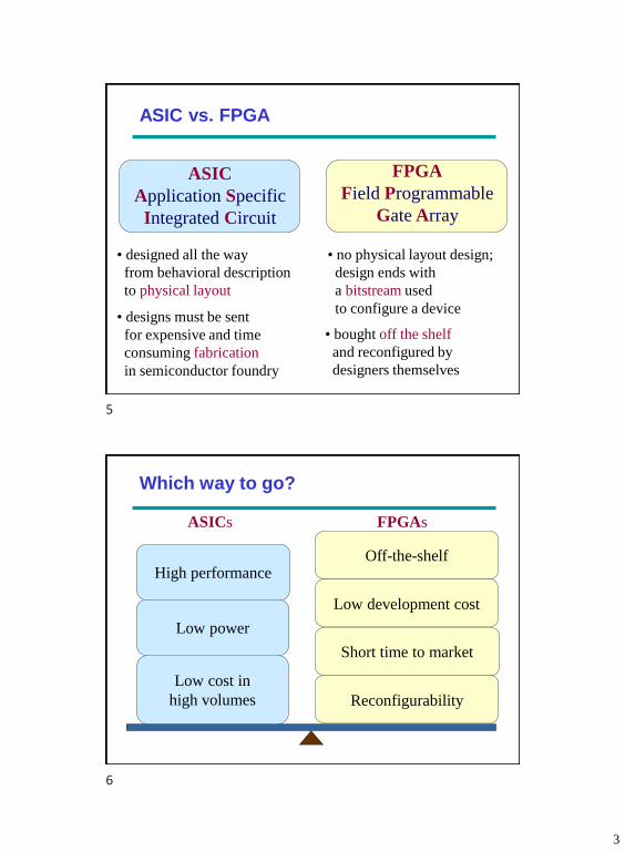
ASIC vs. FPGA
• designs must be sent
for expensive and time
consuming fabrication
in semiconductor foundry
• bought off the shelf
and reconfigured by
designers themselves
ASIC
Application Specific
Integrated Circuit
FPGA
Field Programmable
Gate Array
• designed all the way
from behavioral description
to physical layout
• no physical layout design;
design ends with
a bitstream used
to configure a device
Which way to go?
Off-the-shelf
Low development cost
Short time to market
Reconfigurability
High performance
ASICs FPGAs
Low power
Low cost in
high volumes
5
6
4
• Custom ICs are very expensive to develop, and delay introduction of
product to market (time to market) because of increased design time.
• Note: need to worry about two kinds of costs:
• 1. cost of development, called non-recurring engineering (NRE)
• 2. cost of manufacture
• A tradeoff usually exists between NRE cost and manufacturing costs
totalcosts
number of units manufactured (volume)
NRE
A
B
Why FPGAs?
ASICs
FPGAs
Applications of FPGAs
▪ Implementation of random logic• easier changes at system-level (one device is modified)
• can eliminate need for full-custom chips
▪ Prototyping• ensemble of gate arrays used to emulate a circuit to be
manufactured
• get more/better/faster debugging done than possible with simulation
▪ Reconfigurable hardware• one hardware block used to implement more than one function
• functions must be mutually-exclusive in time
• can greatly reduce cost while enhancing flexibility
▪ Special-purpose computation engines• hardware dedicated to solving one problem (or class of problems)
• accelerators attached to general-purpose computers
7
8
5
Applications of FPGAs
• Early on, used to serve as “glue logic” and for prototyping. Now? Everywhere!– Communications, software-defined radio, digital signal processing,
ASIC prototyping, computer hardware emulation, medical imaging, computer vision, automotive, speech recognition, cryptography, bioinformatics, financial, bitcoin, …
– https://www.altera.com/products/fpga/arria-series/arria-10/applications.html
– https://www.xilinx.com/applications.html
– https://www.xilinx.com/about/customer-innovation/aerospace-and-defense/mars-exploration-rovers.html
– HW accelerators in datacenter servers (Intel purchased Altera for $16 billion).
9
Major FPGA Vendors
SRAM-based FPGAs
▪ Xilinx Inc.
▪ Altera Corp. ($16B Intel 2015)
▪ Atmel ($3.6B Microchip 2016)
▪ Lattice Semiconductor
Flash & antifuse FPGAs
▪ Actel Corp.
▪ Quick Logic Corp.
Share about 90% of the
market
9
10
6
Xilinx FPGA Families
▪ Old families
• XC3000, XC4000, XC5200
• Old 0.5µm, 0.35µm and 0.25µm technology. Not recommended for modern designs.
▪ High-performance families
• Virtex (220 nm)
• Virtex-E, Virtex-EM (180 nm)
• Virtex-II, Virtex-II PRO (130 nm)
• Virtex-4 (90 nm)
• Virtex-5 (65 nm)
• Virtex-6
▪ Low Cost Family
• Spartan/XL – derived from XC4000
• Spartan-II – derived from Virtex
• Spartan-IIE – derived from Virtex-E
• Spartan-3 (90 nm)
• Spartan-3E (90 nm) – logic optimized
• Spartan-3A (90 nm) – I/O optimized
• Spartan-3AN (90 nm) – non-volatile
• Spartan-3A DSP (90 nm) – DSP optimized
• Spartan-6
Zynq-7000
▪ Based on the Xilinx All programmable SoC architecture; 28nm
technology node
▪ ARM dual-core Cortex-A9 MPCore processors
▪ Fixed processing system that can operate independently from the
programmable logic
▪ Processor boots on reset like any processor-based device or ASSP
▪ Processor acts as “system master” and controls the configuration of
the programmable logic enabling full or partial reconfiguration of the
programmable logic during operation
▪ Standard development flows providing a familiar programming
environment for software developers
▪ Additional documentation and resources:
• http://www.xilinx.com/products/silicon-devices/soc/zynq-7000.html
11
12
7
Zynq-7000 Device Family
Z-7010 Z-7015 Z-7020 Z-7030 Z-7045 Z-7100
Processor Core Dual ARM® Cortex™-A9 MPCore™ with CoreSight™
Processor
Extensions
NEON™ & Single / Double Precision Floating Point for each processor
L1 Cache 512 KB
L2 Cache 256 KB
Memory
Interfaces
DDR3, DDR3L, DDR2, LPDDR2, 2x Quad-SPI, NAND, NOR
Peripherals 2x USB 2.0 (OTG), 2x Tri-mode Gigabit Ethernet, 2x SD/SDIO
Logic Cells 28K Logic
Cells
74K Logic
Cells
85K Logic
Cells
125K Logic
Cells
350K Logic
Cells
444K Logic
Cells
BlockRAM
(Mb)
240 KB 380 KB 560 KB 1,060 KB 2,180 KB 3,020 KB
DSP Slices 80 160 220 400 900 2,020
Transceiver
Count
4 (6.25 Gb/s) up to 8 (12.5
Gb/s)
up to 16 (12.5
Gb/s)
up to
16 (10.3125
Gb/s)
Zynq-7000
Diagram
13
14
8
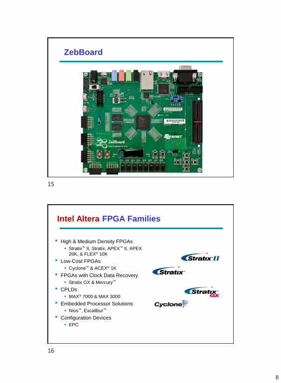
ZebBoard
Intel Altera FPGA Families
• High & Medium Density FPGAs
▪ Stratix™ II, Stratix, APEX™ II, APEX
20K, & FLEX® 10K
• Low-Cost FPGAs
▪ Cyclone™ & ACEX® 1K
• FPGAs with Clock Data Recovery
▪ Stratix GX & Mercury™
• CPLDs
▪ MAX® 7000 & MAX 3000
• Embedded Processor Solutions
▪ Nios™, Excalibur™
• Configuration Devices
▪ EPC
15
16
9
Altera: Cyclone V
▪ Extends the Cyclone FPGA series
▪ Wide spectrum of general logic
applications
▪ Up to 300,000 logic elements (LEs)
▪ Additional documentation and resources:
• https://www.altera.com/products/fpga/cyclone-
series/cyclone-v/features.html
Cyclone V Key Architectural Features
17
18
10
Cyclone V Devices
19
20
11
21
Logic Element (LE)
▪ The smallest unit of logic located in a LAB of all Altera devices supported by the Quartus software.
▪ Logic element (LE) is also generally known as a logic cell.
▪ In supported device (Arria series, Cyclone series, and Stratix series) family devices, a logic element consists of:
• a four-input LUT
• a programmable register
• a carry chain
https://www.edn.com/Home/PrintView?contentItemId=4015097
Adaptive Logic Module (ALM)
▪ Basic building block of supported device (Arria series,
Cyclone V, Stratix IV, and Stratix V) families
▪ Contains among others:
• two or four register logic cells
• two combinational logic cells
• two dedicated full adders
• a carry chain
• a register chain
▪ http://quartushelp.altera.com/15.0/mergedProjects/refer
ence/glossary/def_alm.htm
▪ http://quartushelp.altera.com/15.0/master.htm#merged
Projects/quartus/gl_quartus_welcome.htm
21
22
12
8-input Adaptive Logic Module (ALM)
23
24
13
DE1-SoC Board
▪ $175 USD (academic)
▪ FPGA Device
• Cyclone V SoC 5CSEMA5F31C6 Device
• Dual-core ARM Cortex-A9 (HPS)
• 85K Programmable Logic Elements
• 4,450 Kbits embedded memory
• 6 Fractional PLLs
• 2 Hard Memory Controllers
▪ Built-in USB Blaster for FPGA programming
▪ http://www.terasic.com.tw/cgi-bin/page/archive.pl?Language=English&CategoryNo=205&No=836&PartNo=2
Overview
▪ FPGA Devices
• ASIC vs. FPGA
• FPGA architecture
▪ FPGA Design Flow
• Synthesis
• Place
• Route
25
26
14
FPGA Architecture – General
27
FPGA Architecture – Detail
28
27
28
15
1) Configurable Logic Block (CLB)
▪ 4-input look-up table (LUT)
• Implements combinational logic functions (essentially store truth table of the function)
• How do we implement LUT’s?
▪ Register
• Optionally stores output of LUT
4-LUT FF1
0
latchLogic Block set by configuration
bit-stream
4-input "look up table"
OUTPUTINPUTS
> Think of LUT as of memory
that stores truth table of any
Boolean function of 4 inputs!
> The four inputs represent the
“address” from where to read from
this memory!
29
How could you build a generic Boolean
logic circuit? Memories as LUTs
▪ 1-bit memory to
hold boolean
value
▪ Address is vector
of boolean input
values
▪ Contents encode
a boolean function
▪ Read out logical
value (col) for
associated row
memory
N-bit
address
word
2N words
29
30
16
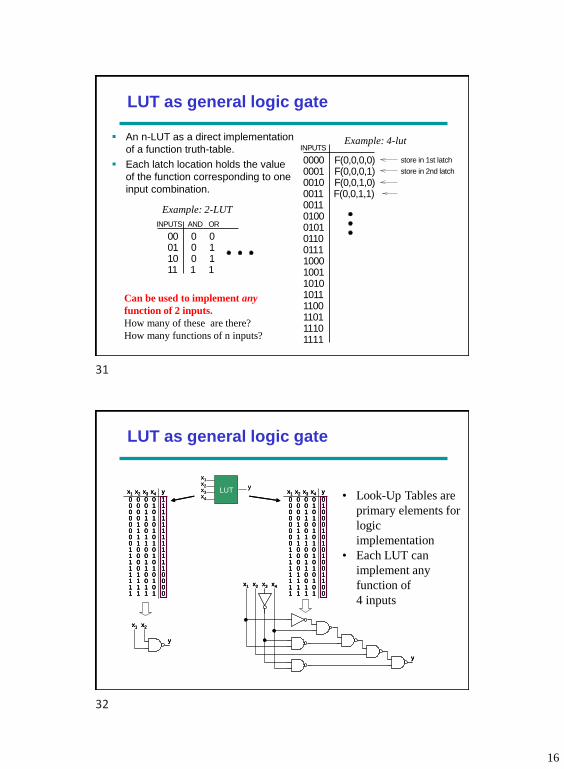
LUT as general logic gate
▪ An n-LUT as a direct implementation
of a function truth-table.
▪ Each latch location holds the value
of the function corresponding to one
input combination.
0000 F(0,0,0,0)0001 F(0,0,0,1)0010 F(0,0,1,0)0011 F(0,0,1,1)0011010001010110011110001001101010111100110111101111
INPUTS
store in 1st latch
store in 2nd latch
Example: 4-lut
Example: 2-LUT
ORANDINPUTS
11 1 110 0 101 0 100 0 0
Can be used to implement any
function of 2 inputs.
How many of these are there?
How many functions of n inputs?
x1 x2 x3 x4
y
x1 x2
y
LUT
x1x2x3x4
y
0
x1
0
x2 x3 x4
0 00 0 0 10 0 1 00 0 1 10 1 0 00 1 0 10 1 1 00 1 1 11 0 0 01 0 0 11 0 1 01 0 1 11 1 0 01 1 0 11 1 1 01 1 1 1
y
0100010101001100
0
x1
0
x2 x3 x4
0 00 0 0 10 0 1 00 0 1 10 1 0 00 1 0 10 1 1 00 1 1 11 0 0 01 0 0 11 0 1 01 0 1 11 1 0 01 1 0 11 1 1 01 1 1 1
y
1111111111110000
x1 x2 x3 x4
y
x1 x2 x3 x4
y
x1 x2
y
x1 x2
y
LUT
x1x2x3x4
y
0
x1
0
x2 x3 x4
0 00 0 0 10 0 1 00 0 1 10 1 0 00 1 0 10 1 1 00 1 1 11 0 0 01 0 0 11 0 1 01 0 1 11 1 0 01 1 0 11 1 1 01 1 1 1
y
0100010101001100
0
x1
0
x2 x3 x4
0 00 0 0 10 0 1 00 0 1 10 1 0 00 1 0 10 1 1 00 1 1 11 0 0 01 0 0 11 0 1 01 0 1 11 1 0 01 1 0 11 1 1 01 1 1 1
y
0100010101001100
0
x1
0
x2 x3 x4
0 00 0 0 10 0 1 00 0 1 10 1 0 00 1 0 10 1 1 00 1 1 11 0 0 01 0 0 11 0 1 01 0 1 11 1 0 01 1 0 11 1 1 01 1 1 1
y
1111111111110000
0
x1
0
x2 x3 x4
0 00 0 0 10 0 1 00 0 1 10 1 0 00 1 0 10 1 1 00 1 1 11 0 0 01 0 0 11 0 1 01 0 1 11 1 0 01 1 0 11 1 1 01 1 1 1
y
1111111111110000
LUT as general logic gate
• Look-Up Tables are
primary elements for
logic
implementation
• Each LUT can
implement any
function of
4 inputs
31
32
17
LUTLUT
X5 X4 X3 X2 X1 Y
0 0 0 0 0 0
0 0 0 0 1 1
0 0 0 1 0 0
0 0 0 1 1 0
0 0 1 0 0 1
0 0 1 0 1 1
0 0 1 1 0 0
0 0 1 1 1 0
0 1 0 0 0 1
0 1 0 0 1 0
0 1 0 1 0 0
0 1 0 1 1 1
0 1 1 0 0 1
0 1 1 0 1 1
0 1 1 1 0 1
0 1 1 1 1 1
1 0 0 0 0 0
1 0 0 0 1 0
1 0 0 1 0 0
1 0 0 1 1 0
1 0 1 0 0 0
1 0 1 0 1 0
1 0 1 1 0 0
1 0 1 1 1 1
1 1 0 0 0 0
1 1 0 0 1 1
1 1 0 1 0 0
1 1 0 1 1 1
1 1 1 0 0 0
1 1 1 0 1 1
1 1 1 1 0 0
1 1 1 1 1 0
LUTLUT
OUT
5-Input functions implemented using two LUTs
multiplexer demultiplexer 4x4 switch
control control
Recall: Multiplexer/Demultiplexer
▪ Multiplexer: route one of many inputs to a single
output
▪ Demultiplexer: route single input to one of many
outputs
33
34
18
▪ 2:1 mux: Z = A' I0 + A I1
▪ 4:1 mux: Z = A' B' I0 + A' B I1 + A B' I2 + A B I3
▪ 8:1 mux: Z = A'B'C'I0 + A'B'CI1 + A'BC'I2 + A'BCI3 +
AB'C'I4 + AB'CI5 + ABC'I6 + ABCI7
I0I1I2I3I4I5I6I7
A B C
8:1mux
ZI0I1I2I3
A B
4:1mux
ZI0I1
A
2:1mux Z
Multiplexers/Selectors: to implement logic
CA B
0
1
2
3
4
5
6
7
1
0
1
0
0
0
1
1
S2
8:1 MUX
S1 S0
F
Multiplexers as LUTs
▪ 2n:1 multiplexer implements any function of n variables
• With the variables used as control inputs and
• Data inputs tied to 0 or 1
• In essence, a look-up table
▪ Example:
• F(A,B,C) = m0 + m2 + m6 + m7
= A'B'C' + A'BC' + ABC' + ABC
= A'B'(C') + A'B(C') + AB'(0) + AB(1)
35
36
19
control signals B and C simultaneously choose one of I0, I1, I2, I3 and one of I4, I5, I6, I7
control signal A chooses which of theupper or lower mux's output to gate to Z
alternativeimplementation
C
Z
A B
4:1mux
2:1mux
2:1mux
2:1mux
2:1mux
I4I5
I2I3
I0I1
I6I7
8:1mux
Cascading Multiplexers
▪ Large multiplexers implemented by cascading smaller
ones
Z
I0I1I2I3
A
I4I5I6I7
B C
4:1mux
4:1mux
2:1mux
8:1mux
latch
latch
latch
latch
16 x 1
mux16
INPUTS
OUTPUT
Latches programmed as partof configuration bit-stream
I0
I1
I2
I3
A B
4:1
muxZ
▪ n-bit LUT is implemented as a 2n x 1 memory:• Inputs choose one of 2n memory locations.
• Memory locations (latches) are normally loaded with values from user’s configuration bit stream.
• Inputs to mux control are the CLB inputs.
▪ Result is a general purpose “logic gate” • n-LUT can implement any function of n
inputs!
• Example:
38
4-LUT Implementation
37
38
20
Example: Xilinx Virtex-E Floorplan
Block RAM
• 4096 bits each
• every 12 CLB columns
Input/Output Blocks
• combinational,
latch, and flipflop
output
• sampled inputs
Configurable Logic Blocks
• 4-input function gens
• buffers
• flipflop
Virtex-E Configurable Logic Block (CLB)
CLB = 4 logic cells (LC) in two slices
LC: 4-input function generator, carry logic, storage element
80 x 120 CLB array on 2000E
16x1 synchronous RAM FF or latch
39
40
21
Details of Virtex-E Slice – implements any two 4-input
functions
4-input
function
3-input
function;
registered
2) Basic I/O Block (IOB) Structure
D
EC
Q
SR
D
EC
Q
SR
D
EC
Q
SR
Three-StateControl
Output Path
Input Path
Three-State
Output
Clock
Set/Reset
Direct Input
Registered Input
FF Enable
FF Enable
FF Enable
41
42
22
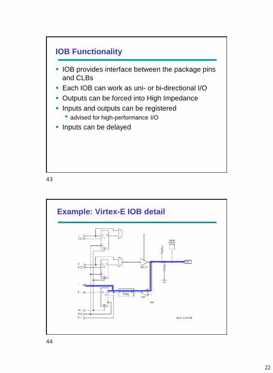
IOB Functionality
▪ IOB provides interface between the package pins
and CLBs
▪ Each IOB can work as uni- or bi-directional I/O
▪ Outputs can be forced into High Impedance
▪ Inputs and outputs can be registered
• advised for high-performance I/O
▪ Inputs can be delayed
Example: Virtex-E IOB detail
43
44
23
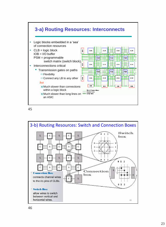
3-a) Routing Resources: Interconnects
▪ Logic blocks embedded in a ‘sea’
of connection resources
▪ CLB = logic block
IOB = I/O buffer
PSM = programmable
switch matrix (switch block)
▪ Interconnections critical
• Transmission gates on paths
Flexibility
Connect any LB to any other
but
Much slower than connections
within a logic block
Much slower than long lines on
an ASIC
3-b) Routing Resources: Switch and Connection Boxes
46
45
46
24
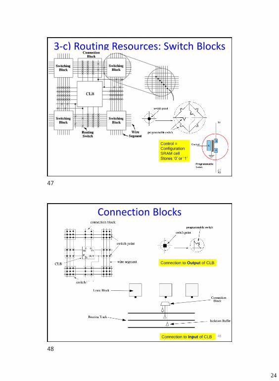
3-c) Routing Resources: Switch Blocks
Control =
Configuration
SRAM cell
Stores ‘0’ or ‘1’
47
Connection Blocks
Connection to Output of CLB
Connection to Input of CLB 48
47
48
25
Example: SRAM-type FPGA Interconnection
SB
Configuring an FPGA
▪ Millions of SRAM cells holding LUTs and Interconnect Routing info
▪ Volatile Memory. Loses configuration when board power is turned off
▪ Keep Bit Pattern describing the SRAM cells in non-Volatile Memory
▪ Configuration takes ~ secs
Configuration data in
Configuration data out
= I/O pin/pad
= SRAM cell
SRAM
JTAG Testing
JTAG Port
Programming
Bit File
49
50
26
Overview
▪ FPGA Devices
• ASIC vs. FPGA
• FPGA architecture
▪ FPGA Design Flow
• Synthesis
• Place
• Route
Typical Digital IC Design Flow Vs.
FPGA Design Flow
51
52
27
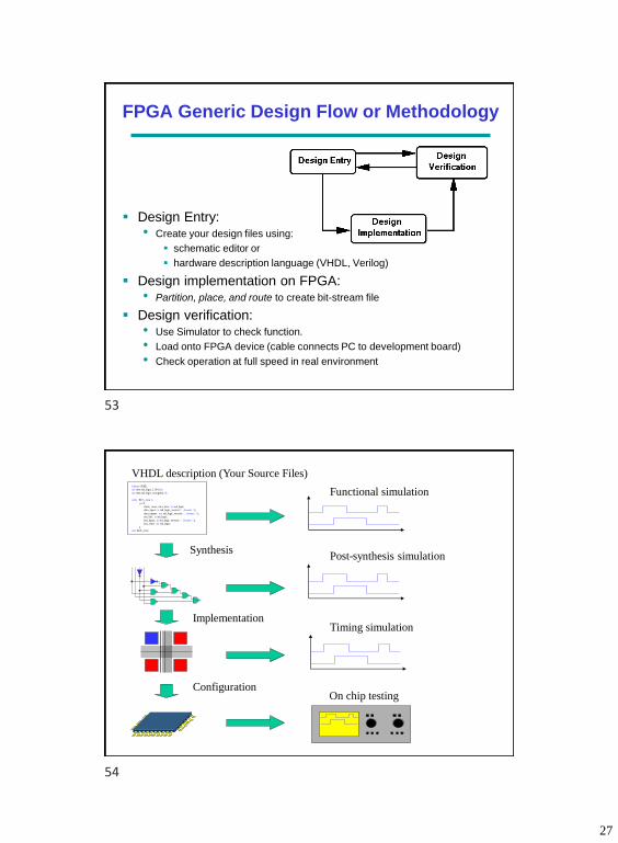
FPGA Generic Design Flow or Methodology
▪ Design Entry:• Create your design files using:
▪ schematic editor or
▪ hardware description language (VHDL, Verilog)
▪ Design implementation on FPGA:• Partition, place, and route to create bit-stream file
▪ Design verification:• Use Simulator to check function.
• Load onto FPGA device (cable connects PC to development board)
• Check operation at full speed in real environment
Library IEEE;
use ieee.std_logic_1164.all;
use ieee.std_logic_unsigned.all;
entity RC5_core is
port(
clock, reset, encr_decr: in std_logic;
data_input: in std_logic_vector(31 downto 0);
data_output: out std_logic_vector(31 downto 0);
out_full: in std_logic;
key_input: in std_logic_vector(31 downto 0);
key_read: out std_logic;
);
end AES_core;
VHDL description (Your Source Files)
Functional simulation
Post-synthesis simulationSynthesis
Implementation
Configuration
Timing simulation
On chip testing
53
54
28
architecture MLU_DATAFLOW of MLU is
signal A1:STD_LOGIC;
signal B1:STD_LOGIC;
signal Y1:STD_LOGIC;
signal MUX_0, MUX_1, MUX_2, MUX_3: STD_LOGIC;
begin
A1<=A when (NEG_A='0') else
not A;
B1<=B when (NEG_B='0') else
not B;
Y<=Y1 when (NEG_Y='0') else
not Y1;
MUX_0<=A1 and B1;
MUX_1<=A1 or B1;
MUX_2<=A1 xor B1;
MUX_3<=A1 xnor B1;
with (L1 & L0) select
Y1<=MUX_0 when "00",
MUX_1 when "01",
MUX_2 when "10",
MUX_3 when others;
end MLU_DATAFLOW;
VHDL description Circuit netlist
Logic Synthesis
Implementation
▪ After synthesis the entire implementation process is
performed by FPGA vendor tools
55
56
29
Translation
Translation
UCF
NGD
EDIF NCF
Native Generic Database file
Constraint Editor
User Constraint File
Native
Constraint
File
Electronic Design
Interchange Format
Circuit netlist Timing Constraints
Synthesis
Pin Assignment
top_level_design
CLOCK
CONTROL(0)
CONTROL(2)
CONTROL(1)
RESET
SEGMENTS(0)
SEGMENTS(1)
SEGMENTS(2)
SEGMENTS(3)
SEGMENTS(4)
SEGMENTS(5)
SEGMENTS(6)
H3
K2G5
K3H1K4
G4
H5
H6
H2
P10
B10FPGA
57
58
30
Circuit Netlist
Mapping
LUT2
LUT3
LUT4
LUT5
LUT1FF1
FF2
LUT0
59
60
31
PlacementCLB SLICES
FPGA
Example placement (VPR tool)
61
62
32
Example placement (ISE tool)
Routing
Programmable Connections
FPGA
63
64
33
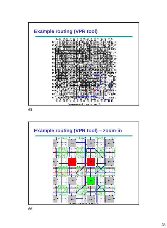
Example routing (VPR tool)
Example routing (VPR tool) – zoom-in
65
66
34
Xilinx FPGA Editor
Configuration
▪ Once a design is implemented, you must create a
file that the FPGA can understand
• This file is called a bitstream: a BIT file (.bit extension)
▪ The BIT file can be downloaded directly to the
FPGA, or can be converted into a PROM file
which stores the programming information
67
68
35
Map report
Design Summary
--------------
Number of errors: 0
Number of warnings: 0
Logic Utilization:
Number of Slice Flip Flops: 30 out of 26,624 1%
Number of 4 input LUTs: 38 out of 26,624 1%
Logic Distribution:
Number of occupied Slices: 33 out of 13,312 1%
Number of Slices containing only related logic: 33 out of 33 100%
Number of Slices containing unrelated logic: 0 out of 33 0%
*See NOTES below for an explanation of the effects of unrelated logic
Total Number 4 input LUTs: 62 out of 26,624 1%
Number used as logic: 38
Number used as a route-thru: 24
Number of bonded IOBs: 10 out of 221 4%
IOB Flip Flops: 7
Number of GCLKs: 1 out of 8 12%
Place & route report
Asterisk (*) preceding a constraint indicates it was not met.
This may be due to a setup or hold violation.
------------------------------------------------------------------------------------------------------
Constraint | Requested | Actual | Logic | Absolute |Number of
| | | Levels | Slack |errors
------------------------------------------------------------------------------------------------------
* TS_CLOCK = PERIOD TIMEGRP "CLOCK" 5 ns | 5.000ns | 5.140ns | 4 | -0.140ns | 5
HIGH 50% | | | | |
------------------------------------------------------------------------------------------------------
TS_gen1Hz_Clock1Hz = PERIOD TIMEGRP "gen1 | 5.000ns | 4.137ns | 2 | 0.863ns | 0
"gen1Hz_Clock1Hz" 5 ns HIGH 50% | | | | |
------------------------------------------------------------------------------------------------------
69
70
36
Post layout timing report
Clock to Setup on destination clock CLOCK
---------------+---------+---------+---------+---------+
| Src:Rise| Src:Fall| Src:Rise| Src:Fall|
Source Clock |Dest:Rise|Dest:Rise|Dest:Fall|Dest:Fall|
---------------+---------+---------+---------+---------+
CLOCK | 5.140| | | |
---------------+---------+---------+---------+---------+
Timing summary:
---------------
Timing errors: 9 Score: 543
Constraints cover 574 paths, 0 nets, and 187 connections
Design statistics:
Minimum period: 5.140ns (Maximum frequency: 194.553MHz)
Summary
▪ FPGAs are more and more prevalent!
▪ They are here to stay!
▪ They offer a flexible platform for increasingly
complex systems
▪ Design automation tools (i.e., CAD tools) take
care of the entire design process from VHDL →
configuration bitstream file
71
72