20
| Date post: | 21-Dec-2015 |
| Category: |
Documents |
| View: | 215 times |
| Download: | 0 times |
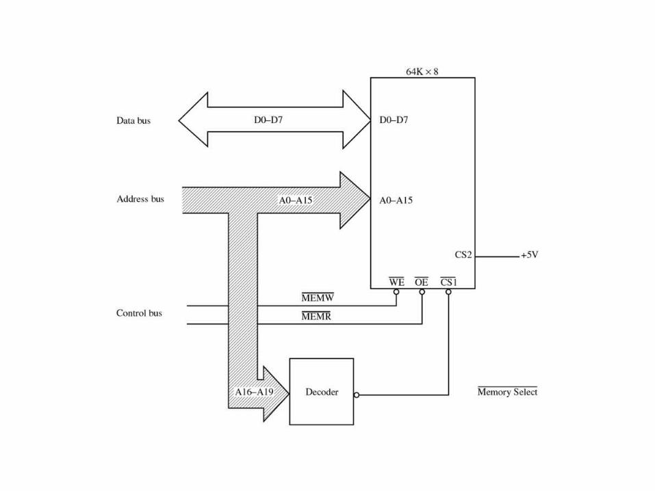
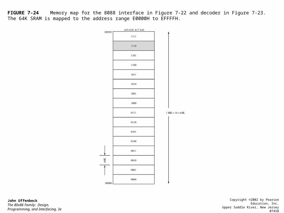
FIGURE 7-24 Memory map for the 8088 interface in Figure 7-22 and decoder in Figure 7-23. The 64K SRAM is mapped to the address range E0000H to EFFFFH.
John UffenbeckThe 80x86 Family: Design, Programming, and Interfacing, 3e
Copyright ©2002 by Pearson Education, Inc.Upper Saddle River, New Jersey 07458
All rights reserved.
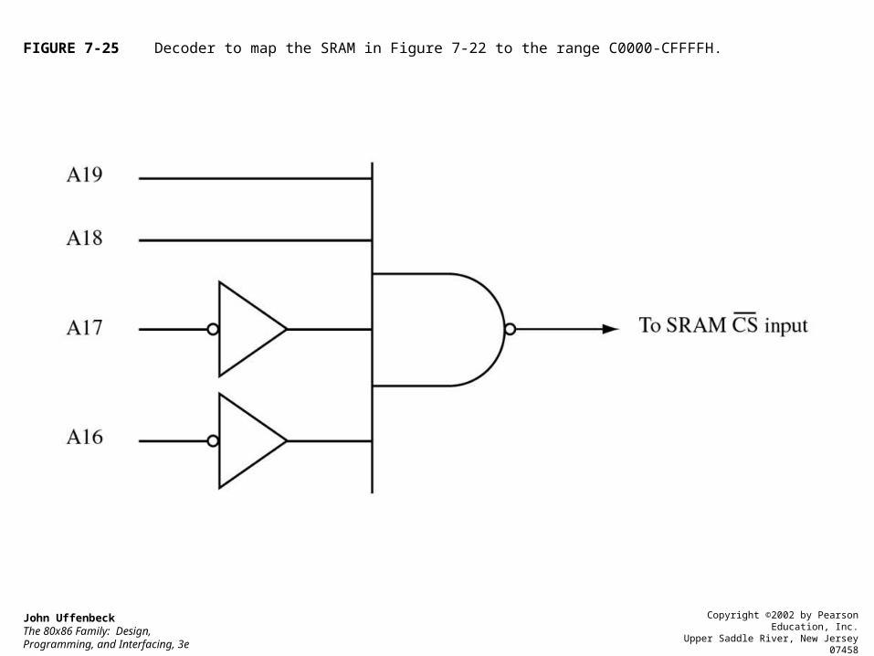
FIGURE 7-25 Decoder to map the SRAM in Figure 7-22 to the range C0000-CFFFFH.
John UffenbeckThe 80x86 Family: Design, Programming, and Interfacing, 3e
Copyright ©2002 by Pearson Education, Inc.Upper Saddle River, New Jersey 07458
All rights reserved.
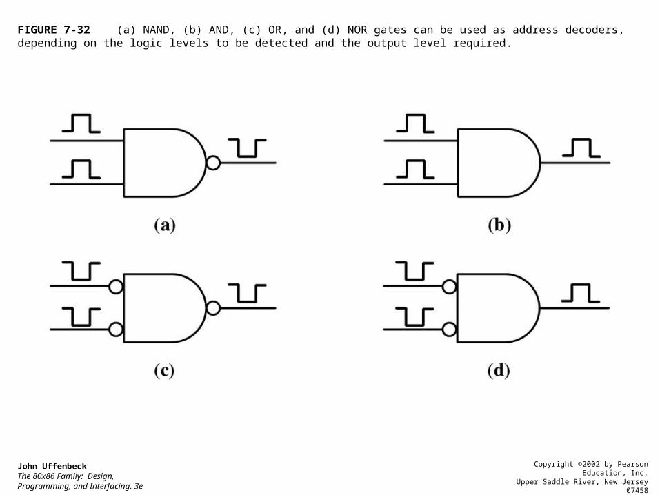
FIGURE 7-32 (a) NAND, (b) AND, (c) OR, and (d) NOR gates can be used as address decoders, depending on the logic levels to be detected and the output level required.
John UffenbeckThe 80x86 Family: Design, Programming, and Interfacing, 3e
Copyright ©2002 by Pearson Education, Inc.Upper Saddle River, New Jersey 07458
All rights reserved.
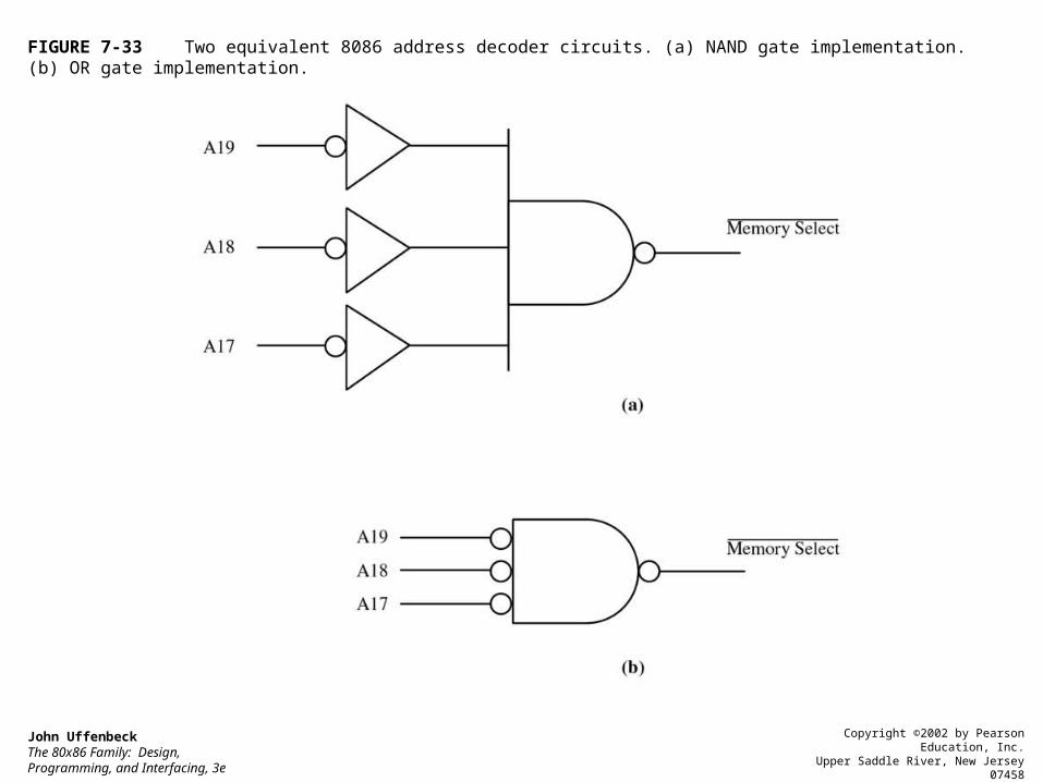
FIGURE 7-33 Two equivalent 8086 address decoder circuits. (a) NAND gate implementation. (b) OR gate implementation.
John UffenbeckThe 80x86 Family: Design, Programming, and Interfacing, 3e
Copyright ©2002 by Pearson Education, Inc.Upper Saddle River, New Jersey 07458
All rights reserved.
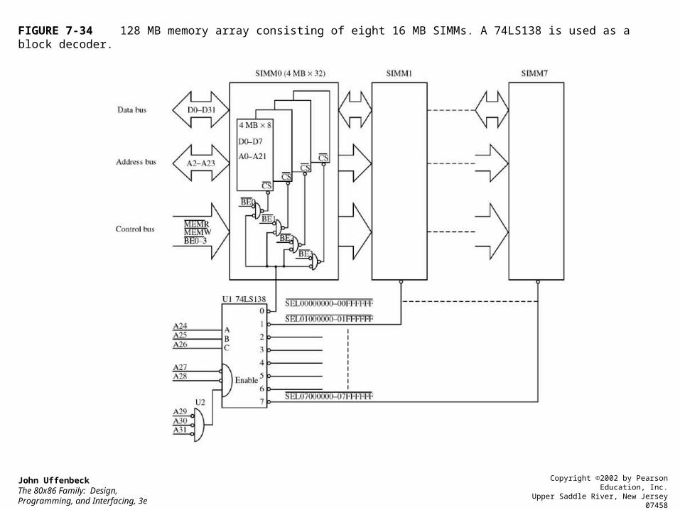
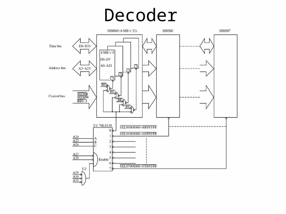
FIGURE 7-34 128 MB memory array consisting of eight 16 MB SIMMs. A 74LS138 is used as a block decoder.
John UffenbeckThe 80x86 Family: Design, Programming, and Interfacing, 3e
Copyright ©2002 by Pearson Education, Inc.Upper Saddle River, New Jersey 07458
All rights reserved.
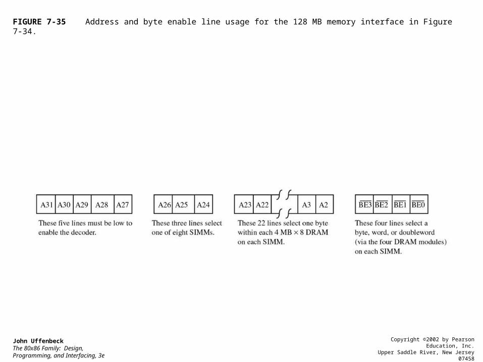
FIGURE 7-35 Address and byte enable line usage for the 128 MB memory interface in Figure 7-34.
John UffenbeckThe 80x86 Family: Design, Programming, and Interfacing, 3e
Copyright ©2002 by Pearson Education, Inc.Upper Saddle River, New Jersey 07458
All rights reserved.
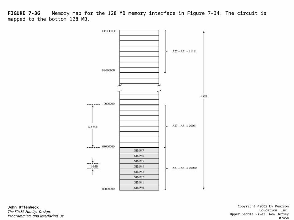
FIGURE 7-36 Memory map for the 128 MB memory interface in Figure 7-34. The circuit is mapped to the bottom 128 MB.
John UffenbeckThe 80x86 Family: Design, Programming, and Interfacing, 3e
Copyright ©2002 by Pearson Education, Inc.Upper Saddle River, New Jersey 07458
All rights reserved.
Decoder
Decoder
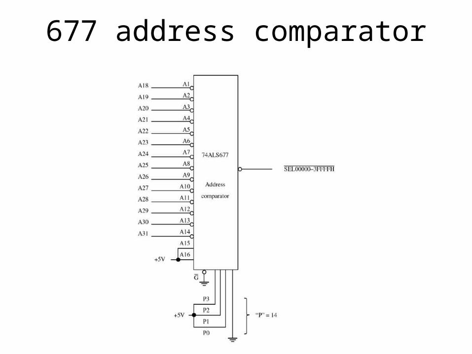
677 address comparator
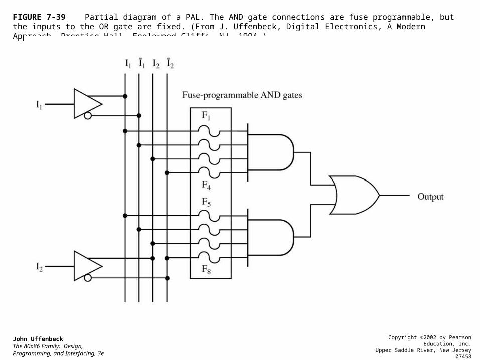
FIGURE 7-39 Partial diagram of a PAL. The AND gate connections are fuse programmable, but the inputs to the OR gate are fixed. (From J. Uffenbeck, Digital Electronics, A Modern Approach, Prentice Hall, Englewood Cliffs, NJ, 1994.)
John UffenbeckThe 80x86 Family: Design, Programming, and Interfacing, 3e
Copyright ©2002 by Pearson Education, Inc.Upper Saddle River, New Jersey 07458
All rights reserved.
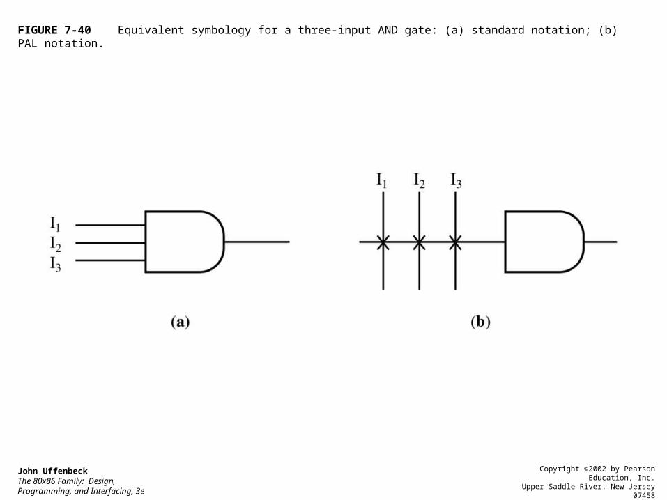
FIGURE 7-40 Equivalent symbology for a three-input AND gate: (a) standard notation; (b) PAL notation.
John UffenbeckThe 80x86 Family: Design, Programming, and Interfacing, 3e
Copyright ©2002 by Pearson Education, Inc.Upper Saddle River, New Jersey 07458
All rights reserved.
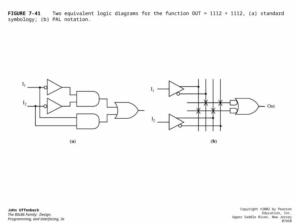
FIGURE 7-41 Two equivalent logic diagrams for the function OUT = 1112 + 1112, (a) standard symbology; (b) PAL notation.
John UffenbeckThe 80x86 Family: Design, Programming, and Interfacing, 3e
Copyright ©2002 by Pearson Education, Inc.Upper Saddle River, New Jersey 07458
All rights reserved.
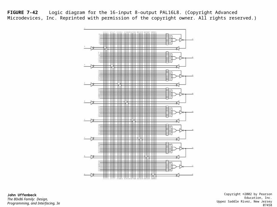
FIGURE 7-42 Logic diagram for the 16-input 8-output PAL16L8. (Copyright Advanced Microdevices, Inc. Reprinted with permission of the copyright owner. All rights reserved.)
John UffenbeckThe 80x86 Family: Design, Programming, and Interfacing, 3e
Copyright ©2002 by Pearson Education, Inc.Upper Saddle River, New Jersey 07458
All rights reserved.
PLA & GLA
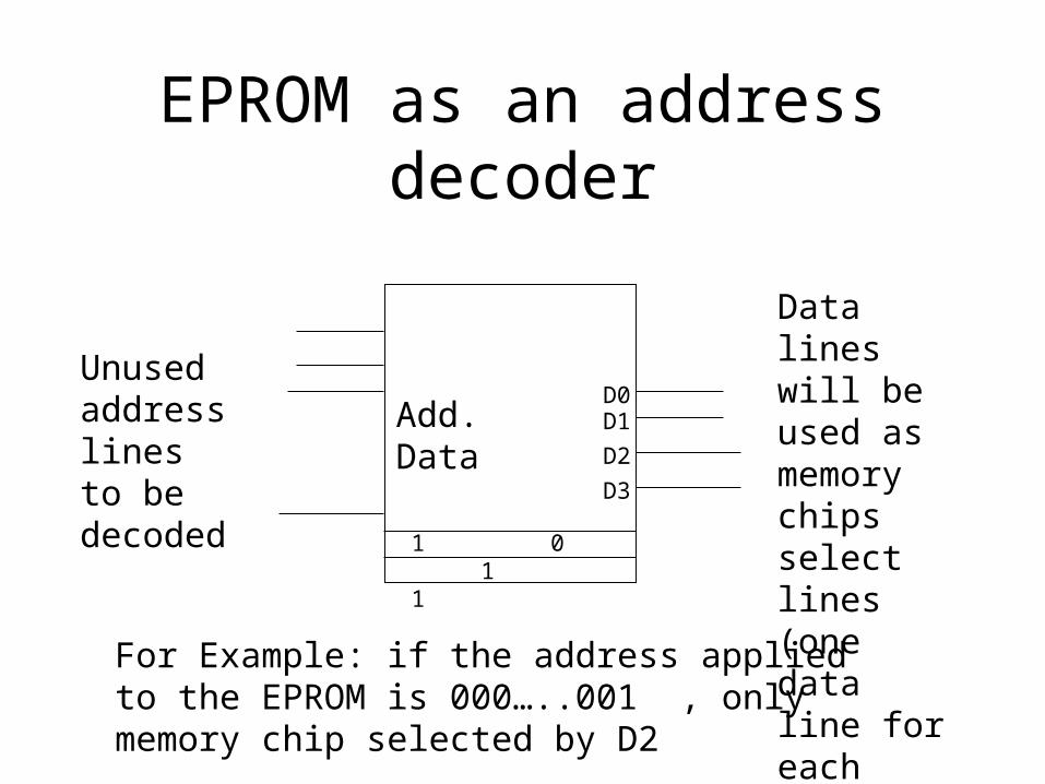
EPROM as an address decoder
Add. Data
Unused address lines to be decoded
Data lines will be used as memory chips select lines (one data line for each chip)1 0 1 1
D3
D0D1
D2
For Example: if the address applied to the EPROM is 000…..001 , only memory chip selected by D2


