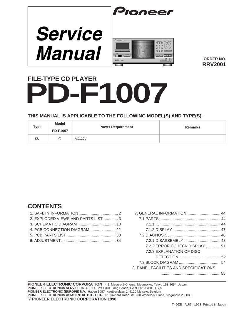
ORDER NO. PIONEER ELECTRONIC CORPORATION 4-1, Meguro 1-Chome, Meguro-ku, Tokyo 153-8654, Japan PIONEER ELECTRONICS SERVICE, INC. P.O. Box 1760, Long Beach, CA 90801-1760, U.S.A. PIONEER ELECTRONIC (EUROPE) N.V. Haven 1087, Keetberglaan 1, 9120 Melsele, Belgium PIONEER ELECTRONICS ASIACENTRE PTE. LTD. 501 Orchard Road, #10-00 Wheelock Place, Singapore 238880 PIONEER ELECTRONIC CORPORATION 1998 FILE-TYPE CD PLAYER RRV2001 T–DZE AUG. 1998 Printed in Japan PD-F1007 1. SAFETY INFORMATION .................................... 2 2. EXPLODED VIEWS AND PARTS LIST ............. 3 3. SCHEMATIC DIAGRAM ................................... 10 4. PCB CONNECTION DIAGRAM ....................... 22 5. PCB PARTS LIST ............................................. 30 6. ADJUSTMENT .................................................. 34 CONTENTS 7. GENERAL INFORMATION .............................. 44 7.1 PARTS ....................................................... 44 7.1.1 IC ....................................................... 44 7.1.2 DISPLAY ........................................... 47 7.2 DIAGNOSIS ................................................ 48 7.2.1 DISASSEMBLY ................................. 48 7.2.2 ERROR CCHECK DISPLAY ............. 51 7.2.3 EXPLANATION OF DISC DETECTION ...................................... 52 7.3 BLOCK DIAGRAM ...................................... 54 8. PANEL FACILITIES AND SPECIFICATIONS ....................................................... 55 THIS MANUAL IS APPLICABLE TO THE FOLLOWING MODEL(S) AND TYPE(S). Type Model PD-F1007 Power Requirement Remarks KU AC120V
Transcript
ORDER NO.
PIONEER ELECTRONIC CORPORATION 4-1, Meguro 1-Chome, Meguro-ku, Tokyo 153-8654, JapanPIONEER ELECTRONICS SERVICE, INC. P.O. Box 1760, Long Beach, CA 90801-1760, U.S.A.PIONEER ELECTRONIC (EUROPE) N.V. Haven 1087, Keetberglaan 1, 9120 Melsele, BelgiumPIONEER ELECTRONICS ASIACENTRE PTE. LTD. 501 Orchard Road, #10-00 Wheelock Place, Singapore 238880 PIONEER ELECTRONIC CORPORATION 1998
FILE-TYPE CD PLAYER
RRV2001
T–DZE AUG. 1998 Printed in Japan
PD-F1007
1. SAFETY INFORMATION.................................... 22. EXPLODED VIEWS AND PARTS LIST ............. 33. SCHEMATIC DIAGRAM ................................... 104. PCB CONNECTION DIAGRAM ....................... 225. PCB PARTS LIST ............................................. 306. ADJUSTMENT .................................................. 34
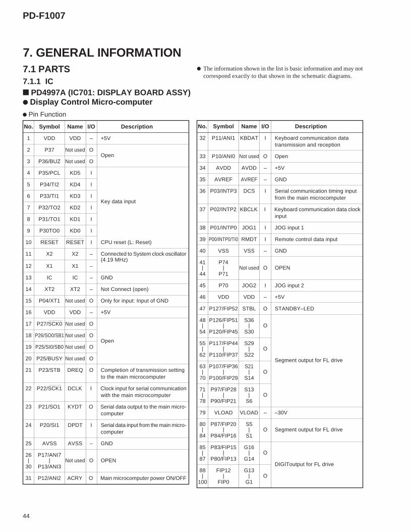
CONTENTS7. GENERAL INFORMATION .............................. 44
7.1 PARTS ....................................................... 447.1.1 IC ....................................................... 447.1.2 DISPLAY ........................................... 47
THIS MANUAL IS APPLICABLE TO THE FOLLOWING MODEL(S) AND TYPE(S).
TypeModel
PD-F1007Power Requirement Remarks
KU AC120V
PD-F1007
2
1. SAFETY INFORMATION
1. SAFETY PRECAUTIONS The following check should be performed for thecont inued protect ion of the customer and servicetechnician.
ANY MEASUREMENTS NOT WITHIN THE LIMITSOUTLINED ABOVE ARE INDICATIVE OF A PO-TENTIAL SHOCK HAZARD AND MUST BE COR-RECTED BEFORE RETURNING THE APPLIANCETO THE CUSTOMER.
2. PRODUCT SAFETY NOTICE Many electrical and mechanical parts in the appli-ance have special safety related characteristics. Theseare often not evident from visual inspection nor theprotection afforded by them necessarily can be ob-tained by using replacement components rated forvoltage, wattage , etc. Replacement parts which havethese special safety characteristics are identified inthis Service Manual. Electrical components having such features areidentified by marking with a on the schematics andon the parts list in this Service Manual.The use of a substitute replacement component whichdoes not have the same safety characteristics as thePIONEER recommended replacement one, shown inthe parts list in this Service Manual, may create shock,fire, or other hazards. Product Safety is continuously under review andnew instructions are issued from time to time. Forthe latest information, always consult the currentPIONEER Service Manual. A subscription to, or ad-ditional copies of, PIONEER Service Manual may beobtained at a nominal charge from PIONEER.
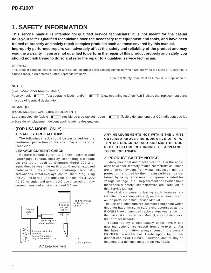
LEAKAGE CURRENT CHECK Measure leakage current to a known earth ground(water pipe, conduit, etc.) by connecting a leakagecur ren t tes ter such as S impson Mode l 229-2 orequivalent between the earth ground and all exposedmetal parts of the appliance (input/output terminals,screwheads, metal overlays, control shaft, etc.). Plugthe AC line cord of the appliance directly into a 120VAC 60 Hz outlet and turn the AC power switch on. Anycurrent measured must not exceed 0.5 mA.
(FOR USA MODEL ONLY)
Also test with plugreversed(Using AC adapterplug as required)
Deviceundertest
Test all exposedmetal surfaces
Earth ground
Leakagecurrenttester
Reading shouldnot be above0.5 mA
AC Leakage Test
REMARQUE
(POUR MODÈLE CANADIEN SEULEMENT)
Les symboles de fusible (fusible de type rapide) et/ou (fusible de type lent) sur CCI indiquent que les
pièces de remplacement doivent avoir la même désignation.
NOTICE
(FOR CANADIAN MODEL ONLY)
Fuse symbols (fast operating fuse) and/or (slow operating fuse) on PCB indicate that replacement parts
must be of identical designation.
This service manual is intended for qualified service technicians; it is not meant for the casualdo-it-yourselfer. Qualified technicians have the necessary test equipment and tools, and have beentrained to properly and safely repair complex products such as those covered by this manual.Improperly performed repairs can adversely affect the safety and reliability of the product and mayvoid the warranty. If you are not qualified to perform the repair of this product properly and safely, youshould not risk trying to do so and refer the repair to a qualified service technician.
WARNING
This product contains lead in solder and certain electrical parts contain chemicals which are known to the state of California to
cause cancer, birth defects or other reproductive harm.
Health & Safety Code Section 25249.6 – Proposition 65
PD-F1007
3
1
6
7
8
9
10
11
12
4
5
3
2
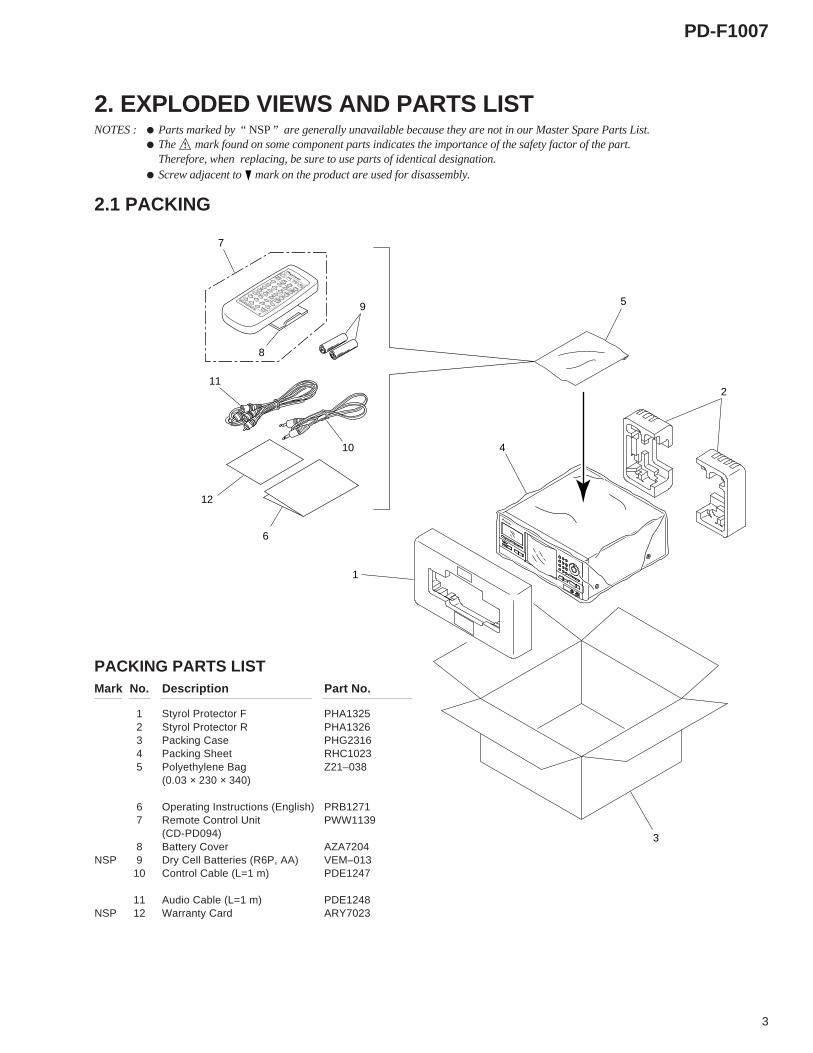
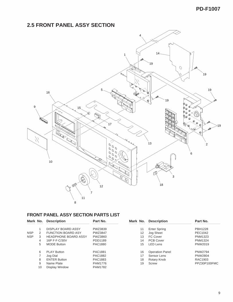
2. EXPLODED VIEWS AND PARTS LIST
2.1 PACKING
PACKING PARTS LIST
1 Styrol Protector F PHA13252 Styrol Protector R PHA13263 Packing Case PHG23164 Packing Sheet RHC10235 Polyethylene Bag Z21–038
(0.03 × 230 × 340)
6 Operating Instructions (English) PRB12717 Remote Control Unit PWW1139
(CD-PD094)8 Battery Cover AZA7204
NSP 9 Dry Cell Batteries (R6P, AA) VEM–01310 Control Cable (L=1 m) PDE1247
11 Audio Cable (L=1 m) PDE1248NSP 12 Warranty Card ARY7023
NOTES : Parts marked by “ NSP ” are generally unavailable because they are not in our Master Spare Parts List.The mark found on some component parts indicates the importance of the safety factor of the part.Therefore, when replacing, be sure to use parts of identical designation.Screw adjacent to mark on the product are used for disassembly.
Mark No. Description Part No.
PD-F1007
4
B
B
A
AI
I
H
C
C
D
D
E
EF G
G
F
H
19
8
21
21
20
18
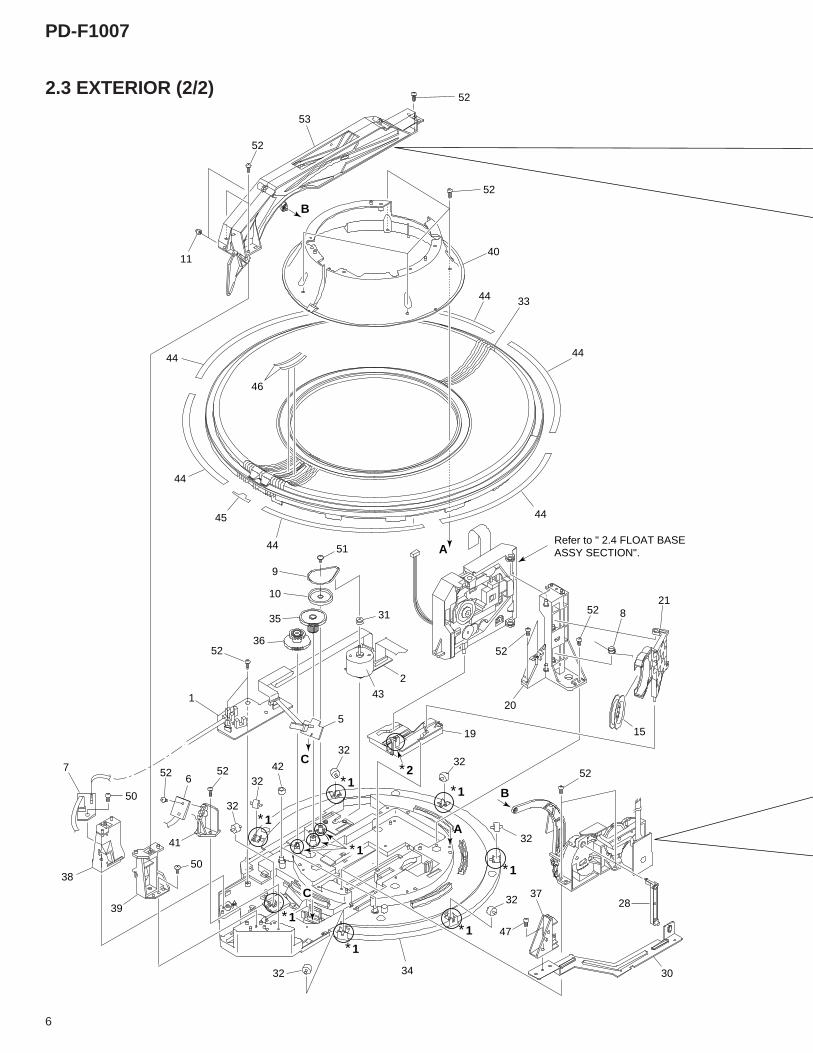
Refer to " 2.3 EXTERIOR (2/2)".
3
6
17
6
15
22
14(1/2)
6
12
16
20
20
20
20
10
20
20
10
23
23
7
4
11 (2/2)
20
20
20
11 (1/2)
2
20
2020
20
22
22
22
13
1
14(2/2)
2020
5
20
Refer to " 2.5 FRONT PANEL ASSY SECTION".
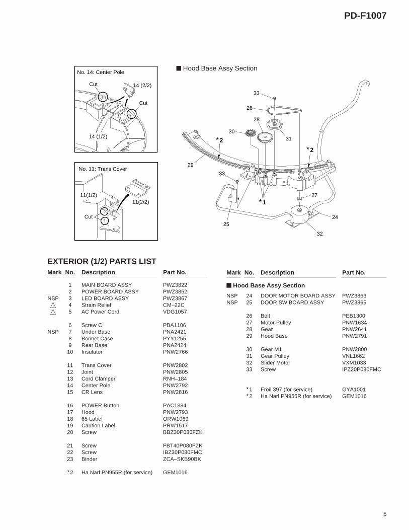
Hood Base Assy
9
∗2
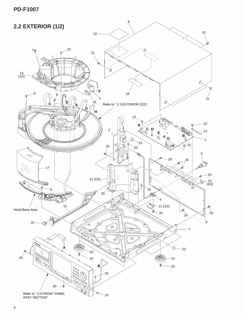
2.2 EXTERIOR (1/2)
PD-F1007
5
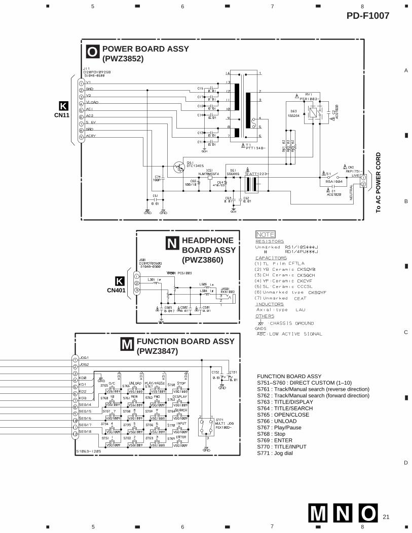
1 MAIN BOARD ASSY PWZ38222 POWER BOARD ASSY PWZ3852
NSP 3 LED BOARD ASSY PWZ38674 Strain Relief CM–22C5 AC Power Cord VDG1057
6 Screw C PBA1106NSP 7 Under Base PNA2421
8 Bonnet Case PYY12559 Rear Base PNA2424
10 Insulator PNW2766
11 Trans Cover PNW280212 Joint PNW280513 Cord Clamper RNH–18414 Center Pole PNW279215 CR Lens PNW2816
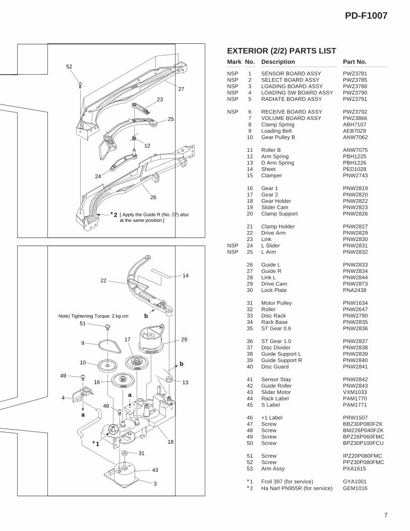
EXTERIOR (2/2) PARTS LISTMark No. Description Part No.
a
a
b
bNote) Tightening Torque: 2 kg·cm
52
23
25
12
24
26
2214
29
51
9
10
4916
17
13
18
3
43
31
48
4
27
∗1
∗2 [ Apply the Guide R (No. 27) also at the same position.]
PD-F1007
8
18
20
23
12
6
11
7
1
8
9
22
21
4
16
3
2
510
17
14
15
24
2519
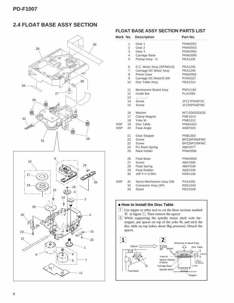
SpacerSpacer
(Pressure of about 9 kg)
Disc Table
1.2mm
6.9mm
0.9mm±0.05mm
Yoke M
Spindle Motor
Carriage Base
Stopper
Spacer SettingPosition
21
1 Use nipper or other tool to cut the three sections marked A in figure 1. Then remove the spacer
2 While supporting the spindle motor shaft with the stopper, put spacer on top of the yoke M, and stick the disc table on top (takes about 9kg pressure). Detach the spacer.
¶ How to Install the Disc Table
AA
Float Base
29
29
28
3026
33
27
31
32
1 Gear 1 PNW20522 Gear 2 PNW20533 Gear 3 PNW20544 Carriage Base PNW26995 Pickup Assy - S PEA1335
6 D.C. Motor Assy (SPINDLE) PEA12357 Carriage DC Motor Assy PEA12468 Pinion Gear PNW20559 Carriage DC Motor/0.3W PXM102710 Disc Table Assy PEA1314
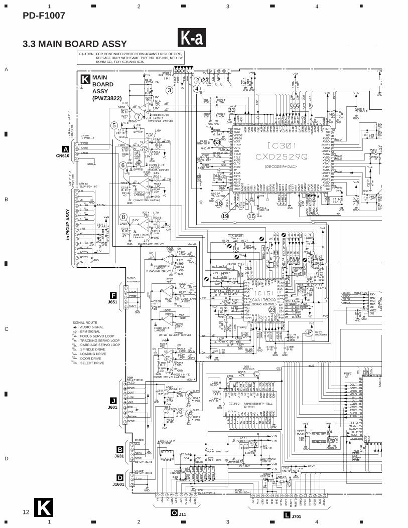
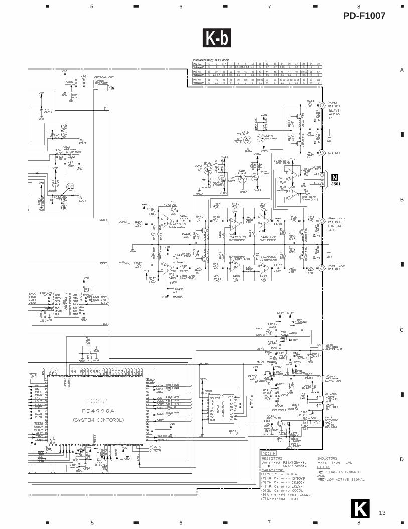
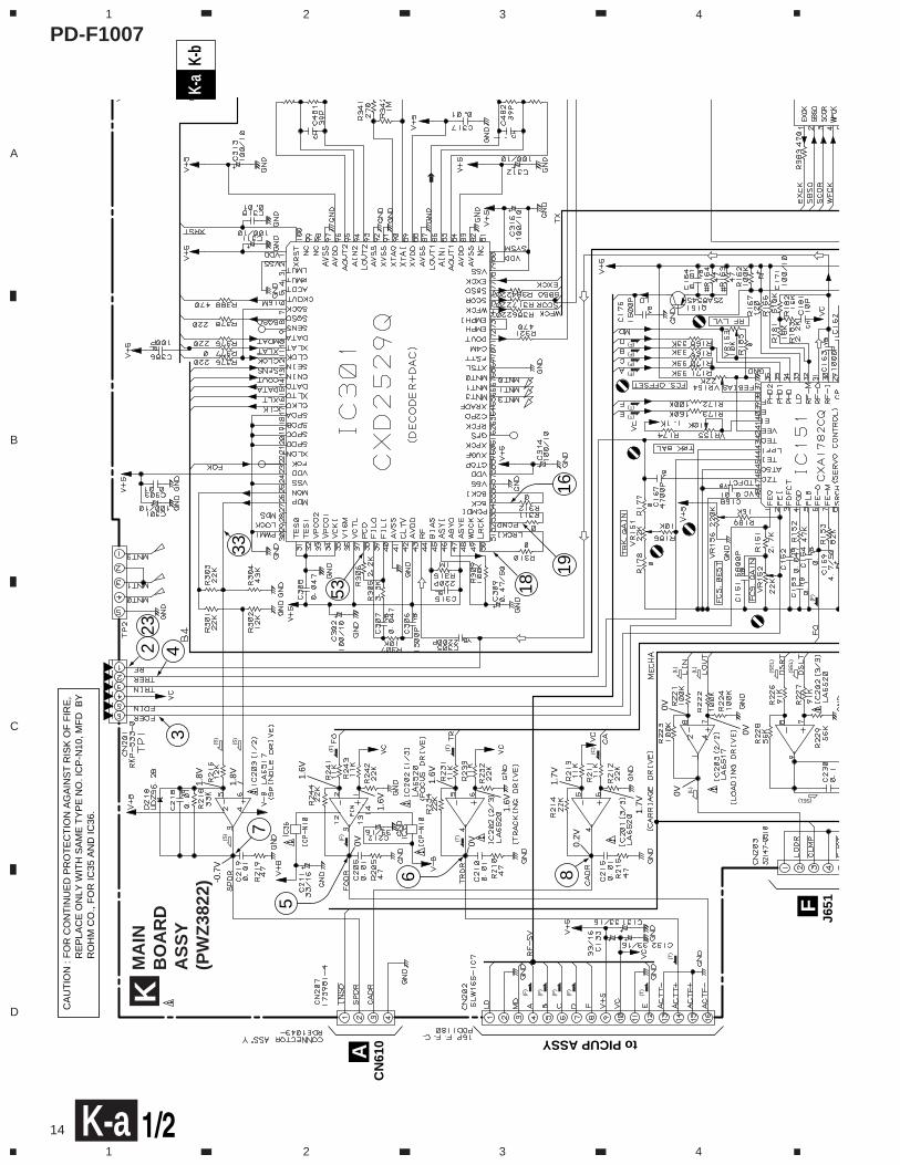
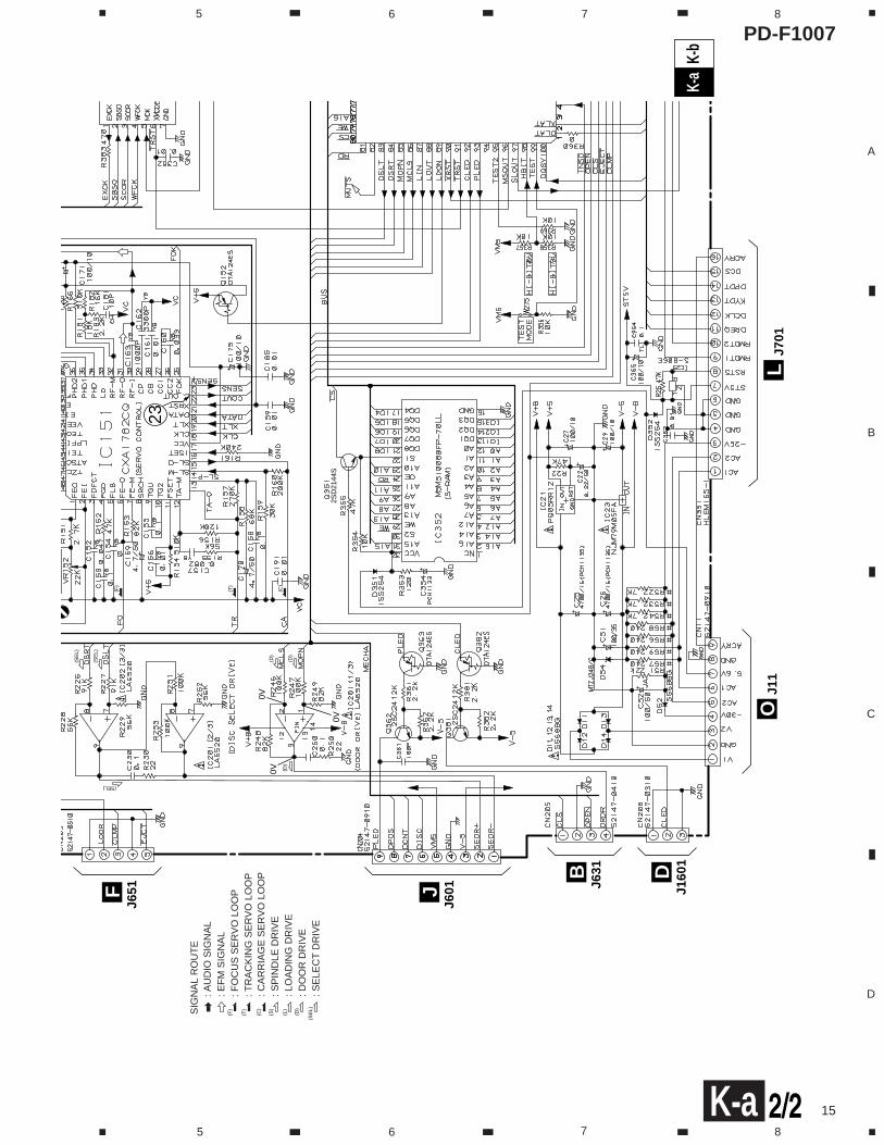
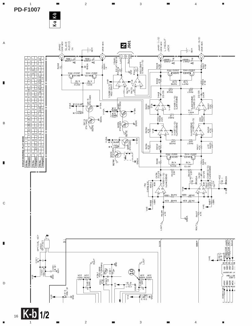
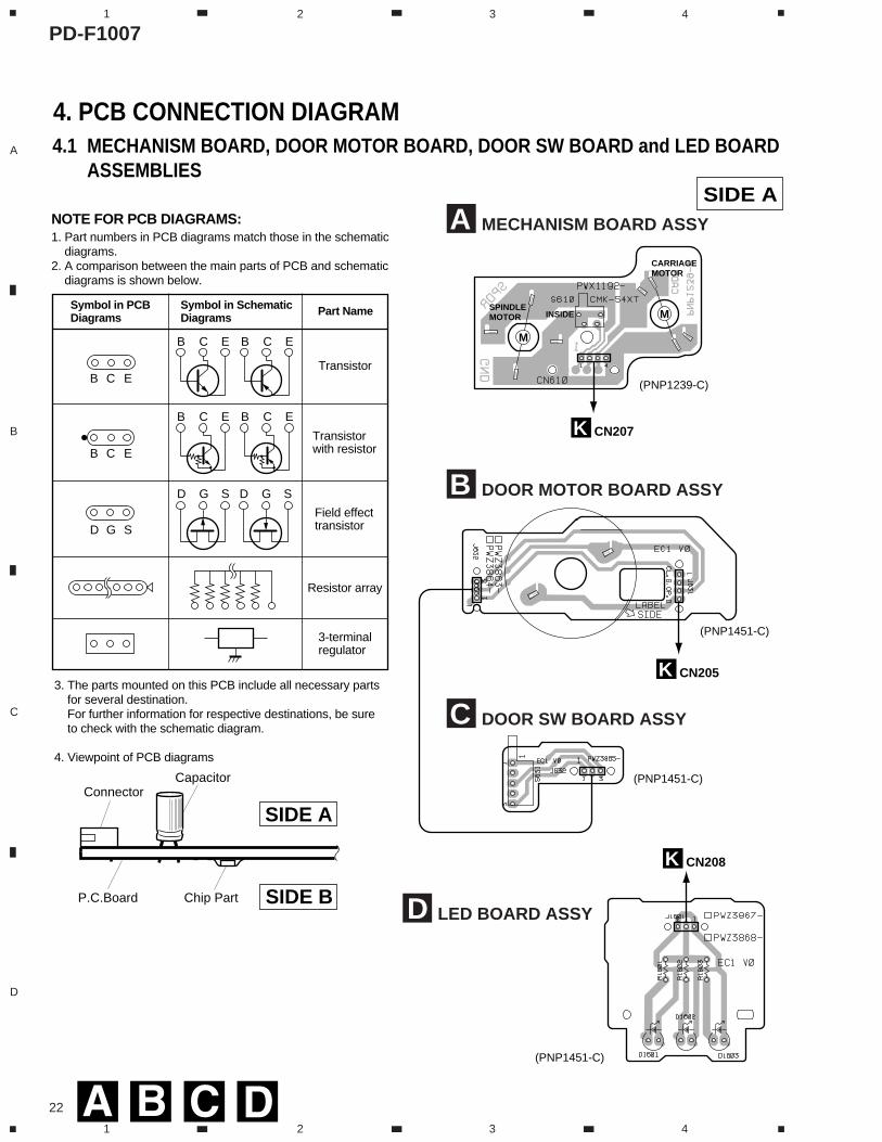
NOTE FOR PCB DIAGRAMS:1. Part numbers in PCB diagrams match those in the schematic diagrams.2. A comparison between the main parts of PCB and schematic diagrams is shown below.
3. The parts mounted on this PCB include all necessary parts for several destination. For further information for respective destinations, be sure to check with the schematic diagram.
4. Viewpoint of PCB diagrams
Symbol in PCBDiagrams
Symbol in SchematicDiagrams Part Name
Transistor
Transistorwith resistor
Field effecttransistor
Resistor array
3-terminalregulator
B C E
B C E
B C E
D G S
B C E
B C E B C E
D G S D G S
CapacitorConnector
P.C.Board Chip Part
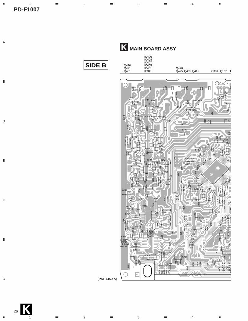
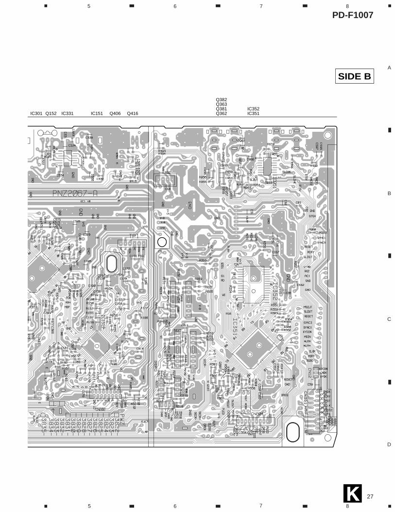
SIDE A
SIDE B
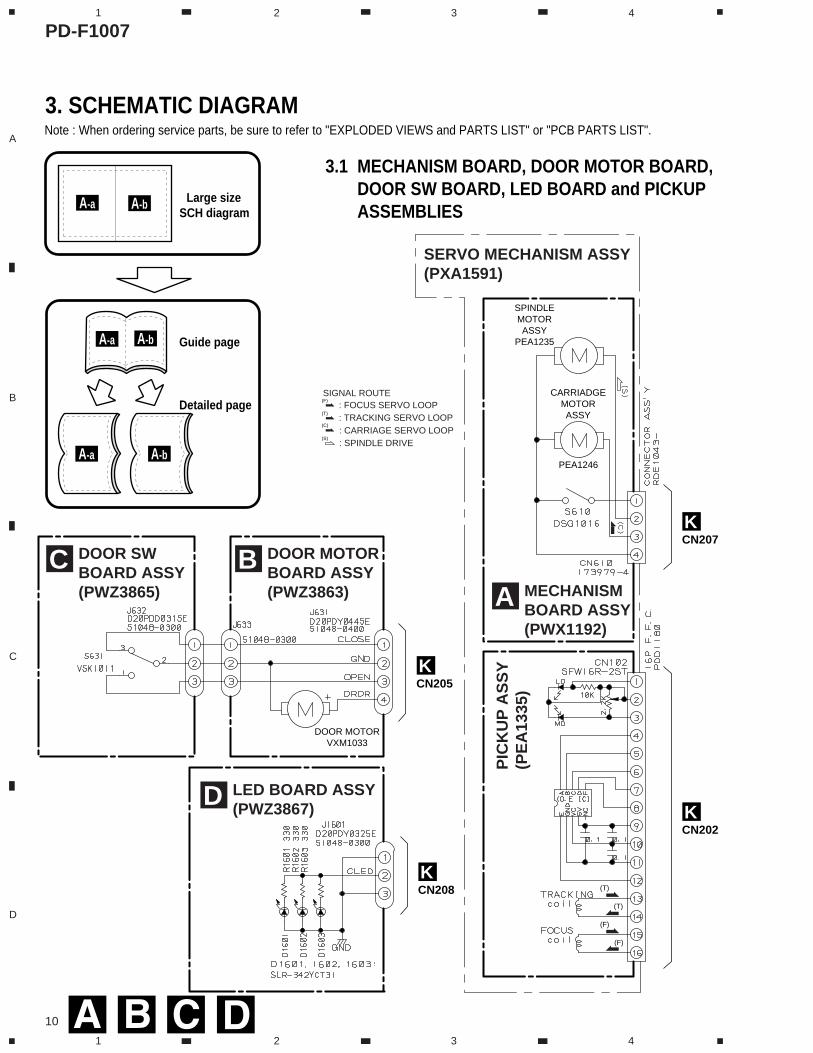
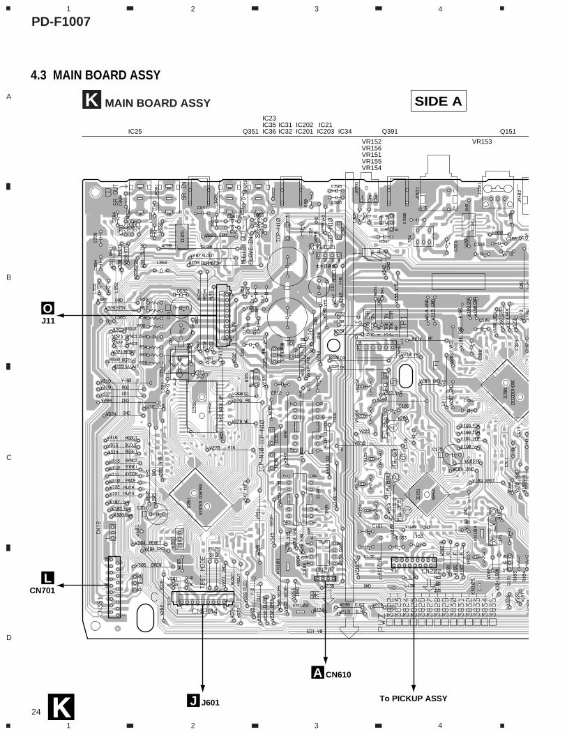
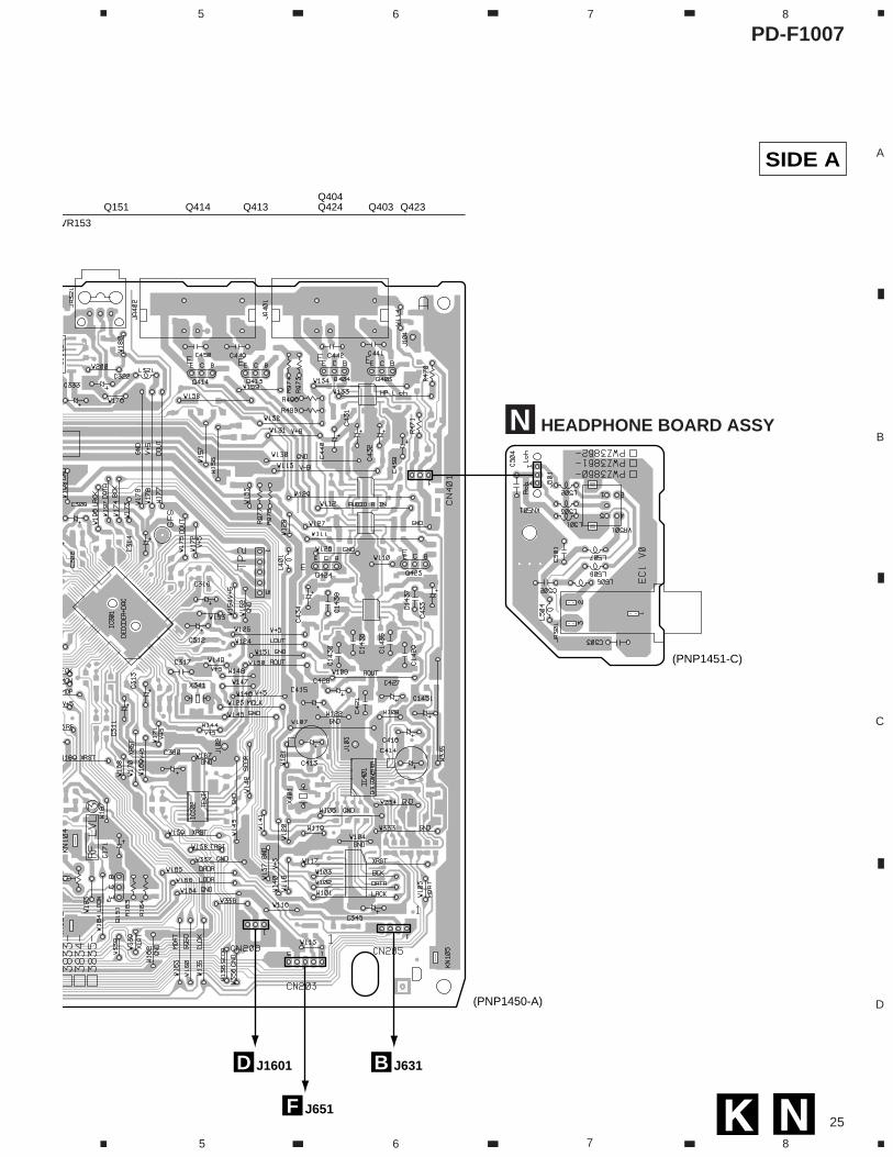
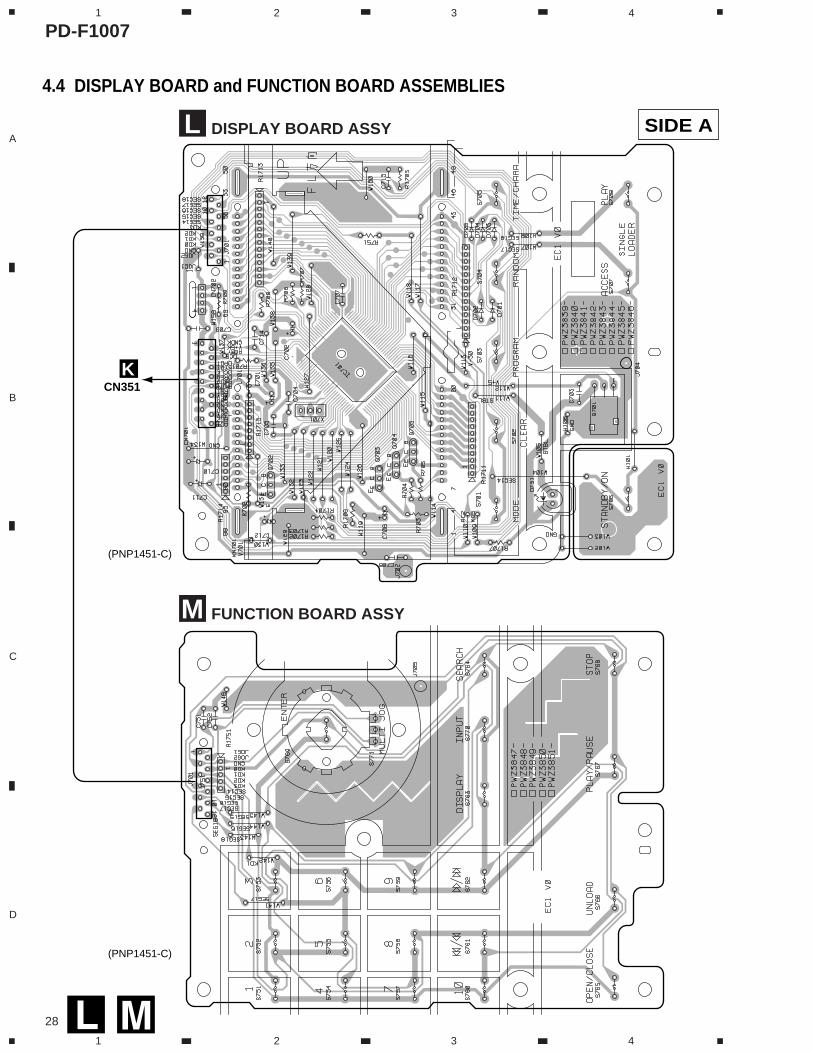
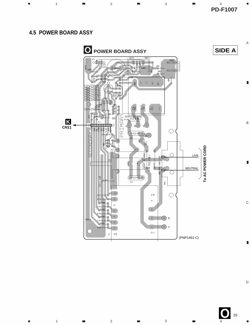
4. PCB CONNECTION DIAGRAM
MECHANISM BOARD ASSYA
DOOR MOTOR BOARD ASSYB
DOOR SW BOARD ASSYC
LED BOARD ASSYD
CARRIAGEMOTOR
MSPINDLEMOTOR
M
INSIDE
K CN207
K CN205
K CN208
(PNP1239-C)
(PNP1451-C)
(PNP1451-C)
(PNP1451-C)
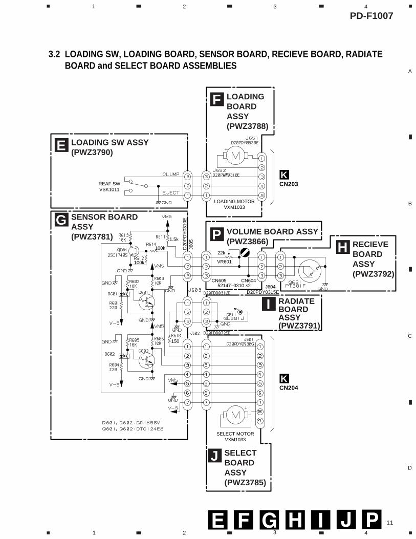
4.1 MECHANISM BOARD, DOOR MOTOR BOARD, DOOR SW BOARD and LED BOARD ASSEMBLIES
Mark No. Description Part No. Mark No. Description Part No.
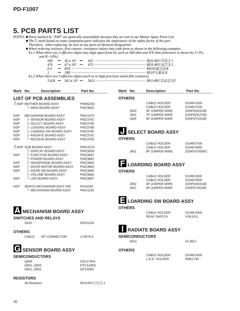
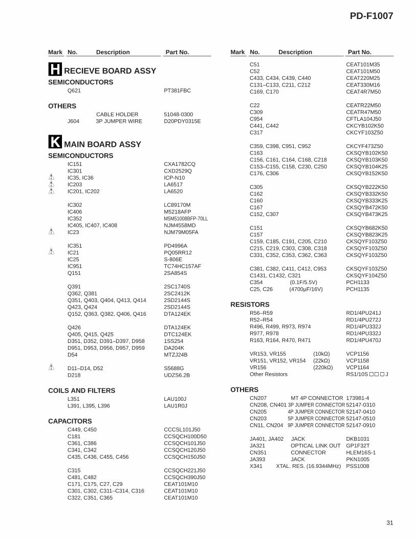
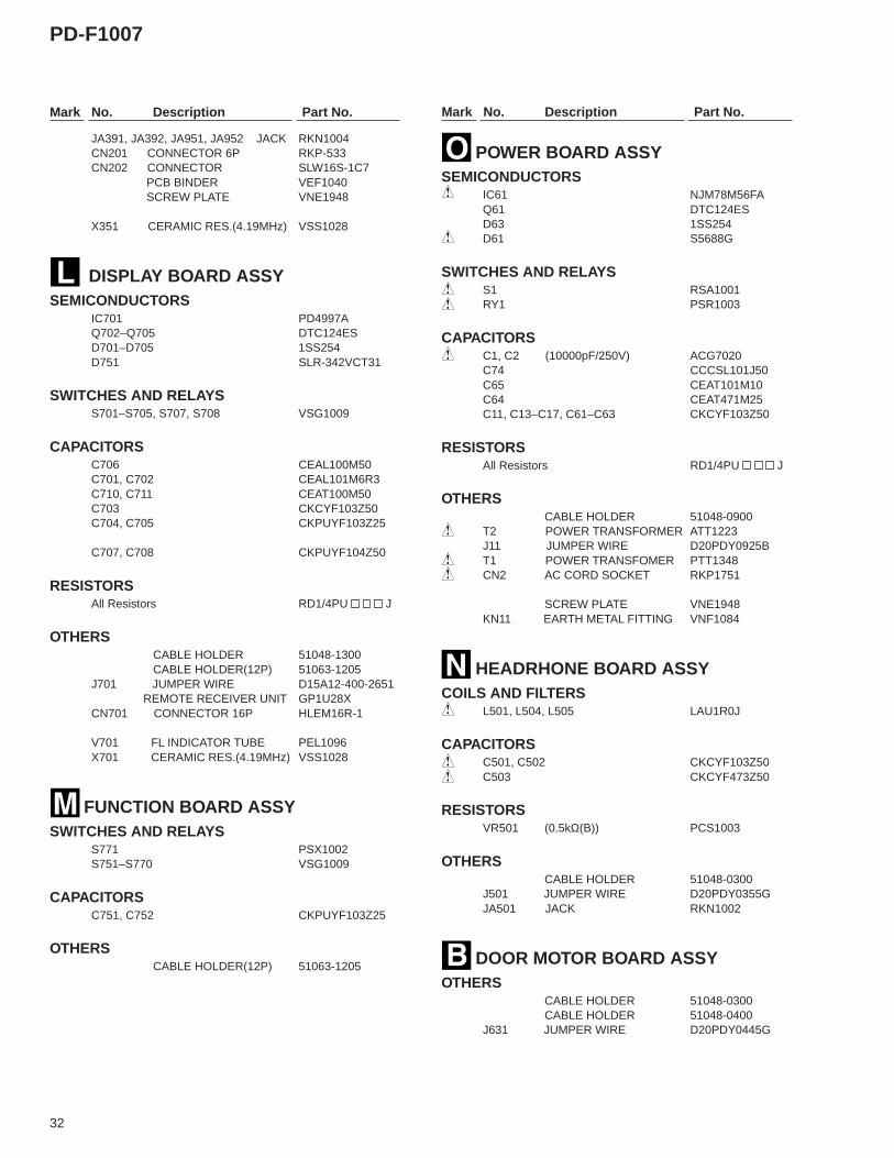
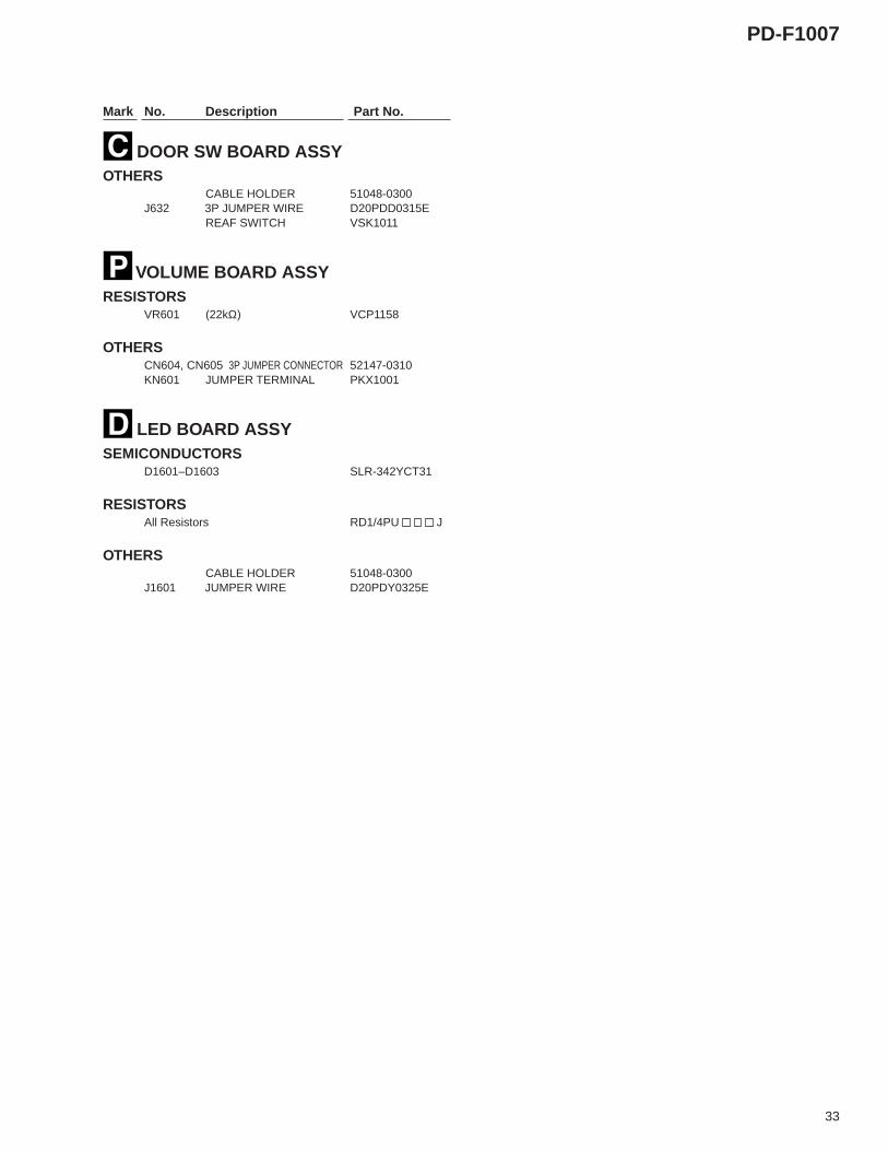
5. PCB PARTS LISTParts marked by "NSP" are generally unavailable because they are not in our Master Spare Parts List.The mark found on some component parts indicates the importance of the safety factor of the part.Therefore, when replacing, be sure to use parts of identical designation.When ordering resistors, first convert resistance values into code form as shown in the following examples.Ex.1 When there are 2 effective digits (any digit apart from 0), such as 560 ohm and 47k ohm (tolerance is shown by J=5%, and K=10%).
Ex.2 When there are 3 effective digits (such as in high precision metal film resistors).
5 6 14 7 3
R 5 01 R 0
5 6 2 1
NOTES:
56047k 0.51
RD1/4PU JRD1/4PU JRN2H KRS1P K
56 x 101
47 x 103 R501R0
561473
5.62k RN1/4PC F562 x 101 5621
LIST OF PCB ASSEMBLIESNSP MOTHER BOARD ASSY PWM2252
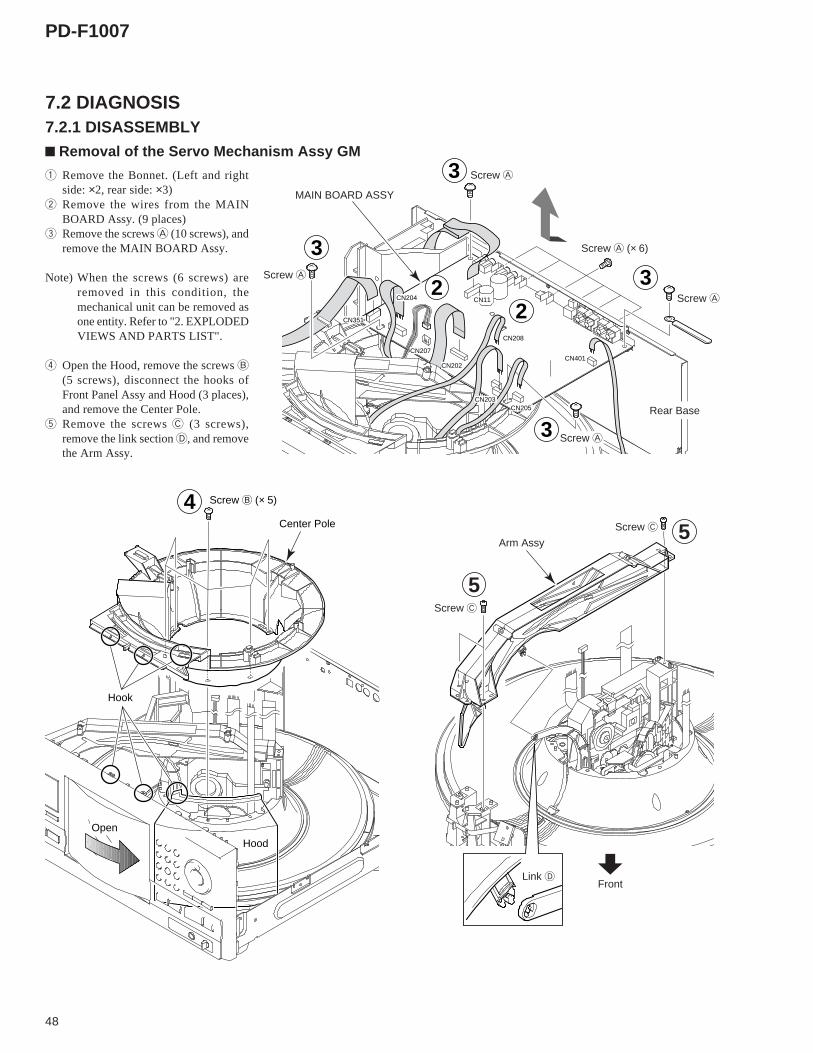
1 Remove the Bonnet. (Left and rightside: ×2, rear side: ×3)
2 Remove the wires from the MAINBOARD Assy. (9 places)
3 Remove the screws A (10 screws), andremove the MAIN BOARD Assy.
Note) When the screws (6 screws) areremoved in this condition, themechanical unit can be removed asone entity. Refer to "2. EXPLODEDVIEWS AND PARTS LIST".
4 Open the Hood, remove the screws B
(5 screws), disconnect the hooks ofFront Panel Assy and Hood (3 places),and remove the Center Pole.
5 Remove the screws C (3 screws),remove the link section D, and removethe Arm Assy.
PD-F1007
49
6
Front
Disc Guard Screw E(× 4)
Connector Assy (4P)
Flexible Flat Cable
Screw G
Float Spring
Float Base AssyFloat Base
Float Rubber
Servo MechanismAssy GM
10 8
89
11
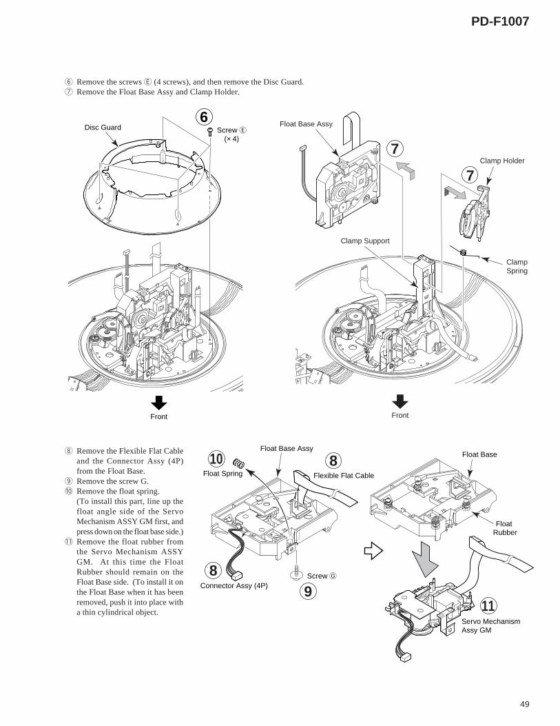
6 Remove the screws E (4 screws), and then remove the Disc Guard.7 Remove the Float Base Assy and Clamp Holder.
8 Remove the Flexible Flat Cableand the Connector Assy (4P)from the Float Base.
9 Remove the screw G.0 Remove the float spring.
(To install this part, line up thefloat angle side of the ServoMechanism ASSY GM first, andpress down on the float base side.)
- Remove the float rubber fromthe Servo Mechanism ASSYGM. At this time the FloatRubber should remain on theFloat Base side. (To install it onthe Float Base when it has beenremoved, push it into place witha thin cylindrical object.
7
7
Front
Clamp Support
Clamp Holder
ClampSpring
Float Base Assy
PD-F1007
50
Disc Rack
Screw A (× 2)
Gear Holder Assy
2
3
Front Panel Assy
Hood
Disconnectthe Hook
Hood Base Assy
Screw B
3
2
Screw B
2
Screw B
2
Disconnect the Hook
Disconnectthe Hooks
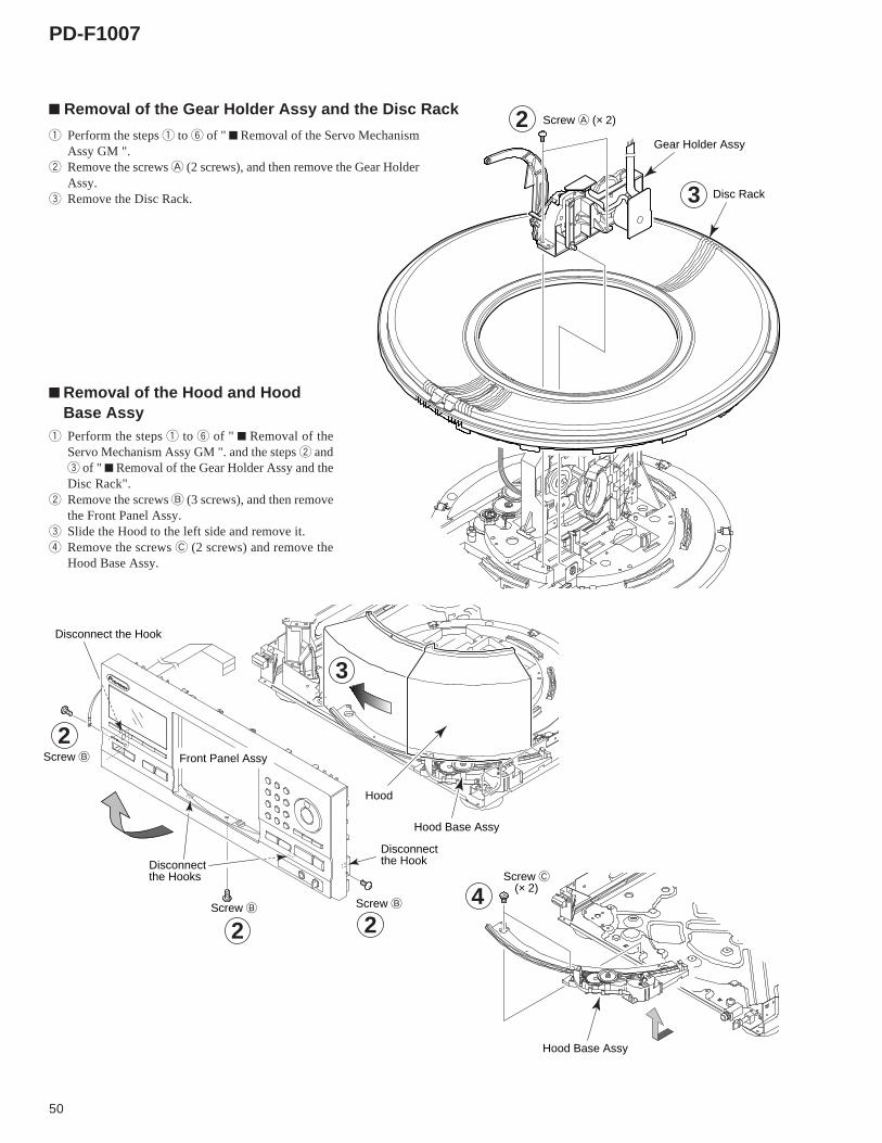
1 Perform the steps 1 to 6 of " Removal of the Servo MechanismAssy GM ".
2 Remove the screws A (2 screws), and then remove the Gear HolderAssy.
3 Remove the Disc Rack.
Removal of the Gear Holder Assy and the Disc Rack
1 Perform the steps 1 to 6 of " Removal of theServo Mechanism Assy GM ". and the steps 2 and3 of " Removal of the Gear Holder Assy and theDisc Rack".
2 Remove the screws B (3 screws), and then removethe Front Panel Assy.
3 Slide the Hood to the left side and remove it.4 Remove the screws C (2 screws) and remove the
Hood Base Assy.
Removal of the Hood and HoodBase Assy
Hood Base Assy
4Screw C
(× 2)
PD-F1007
51
UserDisplay Display Contents
None • Disc playing was tried after loading, butthe disc could not be detected becausethere was no disc,the disc was upside down,the disc was dirty, disc loading had notbeen completed, etc.
• Focus was lost during disc playingbecause of disc scratches, dirt, etc.
None • At the time of track selection during play,or when trying to play, the servomechanism could not move to the positionof the intended track within a fixed time.
• Disc loading was tried, but loading wasnot possible within a fixed time. (The discwas not brought from the rack.)
• It was tried to return the disc to the rack,but the disc could not be returned withina fixed time.
• At the time of disc selection during play,or at the start of play from stoppedcondition, the selection mechanism couldnot move to the position of the intendeddisc within a fixed time.
• After initialization of the selectionmechanism, after selection mechanismNG, etc., forced rack section positiondetection is performed for the selectionmechanism, but detection was notpossible within a fixed time.
None • Playing was tried after disc loading, butnormal disc rotation was not possiblebecausethe disc was upside down,the disc was dirty,disc loading had not been completed, etc.
• During play normal rotation was notpossible because of disc scratches, dirt,etc.
Display Contents
During spindle stop operation
During disc return
During disc selection (during clamping operationat the time of 26)
During setup
During CDR setup operation
During TOC reading
During search operation on the disc
During play operation
During pause operation
During manual search
7.2.2 ERROR CHECK DISPLAY
Error Code
Error History
Error Occurrence Mode
Error check mode (display of the error history for the last 16 times)is entered when the "TIME/CHARA" button is pressed in testmode. By looking at this display, it can be seen in which status themicrocomputer has stopped.
(1) Explanation of the displayDisc No. = Error codeTrack No. = Error historyMin : sec = Error occurrence mode
Press the "TIME/CHARA" button again to check past error codes.This switches the display. The contents of each display are asfollows.
1 Track No.: Error HistoryDisplay is possible from 1 to 16. The smaller numbers haveoccurred more recently. Accordingly, the error No. 1 is the errorwhich has occurred most recently.
2 Min : sec: Error Occurrence ModeThe internal mode at the time of occurrence of the displayed erroris displayed. With Min : sec, the meaning is provided by the firstdigit.
Minutes digits
Display Contents
During hood closing operation and closed condition
During hood opening operation and open condition
Seconds digits
3 Disc No.: Error Code DetailsNote: A used display is displayed only when return to normal
operation after error occurrence is not possible even whenfailsafe operation is performed.
<<< Rack Section >>>
PD-F1007
52
UserDisplay Display Contents
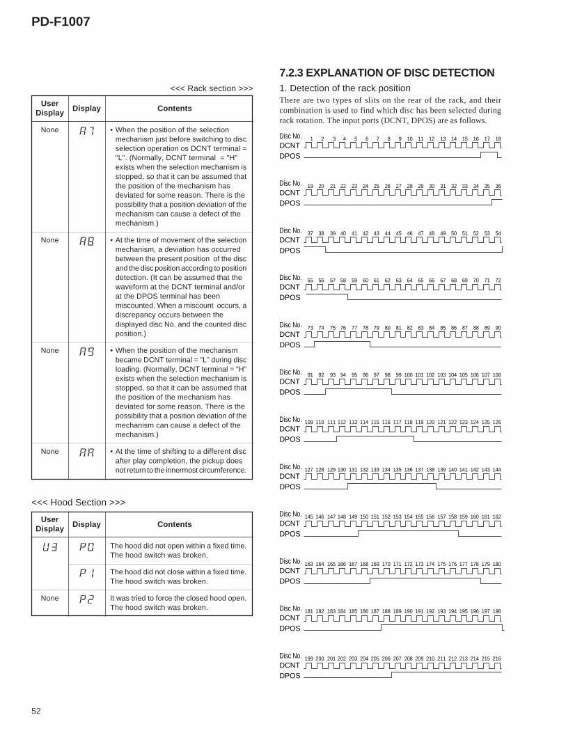
None • When the position of the selectionmechanism just before switching to discselection operation os DCNT terminal ="L". (Normally, DCNT terminal = "H"exists when the selection mechanism isstopped, so that it can be assumed thatthe position of the mechanism hasdeviated for some reason. There is thepossibility that a position deviation of themechanism can cause a defect of themechanism.)
None • At the time of movement of the selectionmechanism, a deviation has occurredbetween the present position of the discand the disc position according to positiondetection. (It can be assumed that thewaveform at the DCNT terminal and/orat the DPOS terminal has beenmiscounted. When a miscount occurs, adiscrepancy occurs between thedisplayed disc No. and the counted discposition.)
None • When the position of the mechanismbecame DCNT terminal = "L" during discloading. (Normally, DCNT terminal = "H"exists when the selection mechanism isstopped, so that it can be assumed thatthe position of the mechanism hasdeviated for some reason. There is thepossibility that a position deviation of themechanism can cause a defect of themechanism.)
None • At the time of shifting to a different discafter play completion, the pickup doesnot return to the innermost circumference.
<<< Rack section >>>
UserDisplay Display Contents
The hood did not open within a fixed time.The hood switch was broken.
The hood did not close within a fixed time.The hood switch was broken.
None It was tried to force the closed hood open.The hood switch was broken.
<<< Hood Section >>>
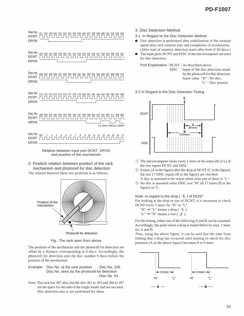
7.2.3 EXPLANATION OF DISC DETECTION1. Detection of the rack positionThere are two types of slits on the rear of the rack, and theircombination is used to find which disc has been selected duringrack rotation. The input ports (DCNT, DPOS) are as follows.
1 The microcomputer looks every 1 msec at the status (H or L) ofthe two inputs DCNT and DISC.
2 8 msec (A in the figure) after the drop of DCNT (C in the figure),the last 17 DISC inputs (B in the figure) are checked.A disc is assumed to be resent when even one of them is "L".
3 No disc is assumed when DISC was "H" all 17 times (B in thefigure) in 2.
Note: In regard to the drop ( ) of DCNTFor looking at the drop or rise of DCNT, it is necessary to checkDCNT every 1 msec for "H" or "L".
"H" = "L" means a drop ( )."L" = "H" means a rise ( ).
For the timing, either one of the following A and B can be assumed.Accordingly, the point where a drop is found differs by max. 1 msecfor A and B.Thus, using the above figure, it can be said that the time fromfinding that a drop has occurred until starting to check for discpresence (A in the above figure) becomes 8 to 9 msec.
Relation between input port DCNT, DPOSand position of the mechanism
2. Position relation between position of the rackmechanism and photocell for disc detection
The relation between these two positions is as follows.
Fig.: The rack seen from above
The position of the mechanism and the photocell for detection areoffset by a distance corresponding to 9 discs. Accordingly, thephotocell for detection sees the disc number 9 discs before theposition of the mechanism.
Example: Disc No. at the rack position : Disc No. 100Disc No. seen by the photocell for detection
: Disc No. 91
Note: The rack has 307 slits, but the slits 301 to 303 and 304 to 307are the space for the side of the single loader and are not used.Disc detection also is not performed for them.
3. Disc Detection Method3-1 In Regard to the Disc Detection Method
Disc detection is performed after stabilization of the rotationspeed after rack rotation start and completion of acceleration.(After start of rotation, detection starts after feed of 20 discs.)The input ports DCNT and DISC of the microcomputer are usedfor disc detection.
Port Explanation : DCNT : As described above.DISC : Input of the disc detection result
by the photocell for disc detection.Input value "H" : No disc,
"L" : Disc present
3-2 In Regard to the Disc Detection Timing
C
DCNT
DISC
A(8msec)
B(16msec)
A B
"H" "L" "H" "L"
1msec 1msec
Photocell for detection
Position of themechanism
PD-F1007
54
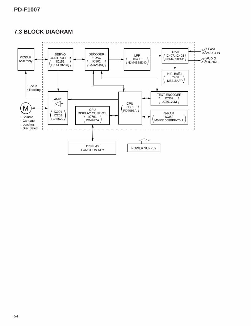
7.3 BLOCK DIAGRAM
PICKUPAssembly
SERVOCONTROLLER
IC151CXA1782CQ
DECODER+ DACIC301
CXD2519Q
S-RAMIC352
M5M51008BPF-70LL
LPFIC405
NJM4558D-DAUDIOSIGNAL
CPUIC351
PD4996A
AMP
IC201IC202
LA6520SpindleCarriageLoadingDisc Select
FocusTracking
M
DISPLAYFUNCTION KEY POWER SUPPLY
.
.
.
.
.
.TEXT ENCODER
IC302LC89170M
CPUDISPLAY CONTROL
IC701PD4997A
BufferIC407, IC408NJM4558D-D
H.P. BufferIC406
M5218AFP
SLAVEAUDIO IN
PD-F1007
55
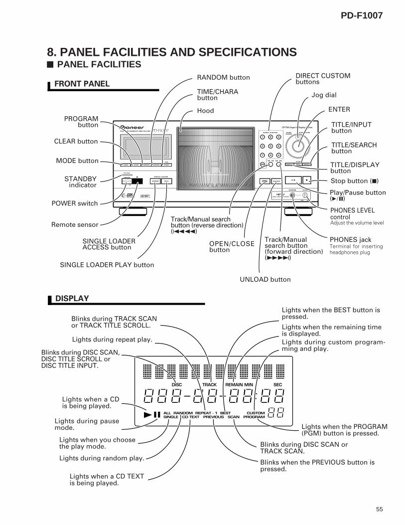
8. PANEL FACILITIES AND SPECIFICATIONS PANEL FACILITIES
FRONT PANEL
Lights when the BEST button ispressed.
Lights when the remaining timeis displayed.
Lights during random play.
Lights during repeat play.
Lights when the PROGRAM(PGM) button is pressed.
Lights when a CDis being played.
Lights during pausemode.
Blinks when the PREVIOUS button ispressed.
Blinks during DISC SCAN,DISC TITLE SCROLL orDISC TITLE INPUT.
Lights during custom program-ming and play.
Lights when you choosethe play mode.
DISPLAY
POWER switch
SINGLE LOADERACCESS button
Hood
Remote sensor
PROGRAMbutton
PHONES jackTerminal for insertingheadphones plug
PHONES LEVELcontrolAdjust the volume level
Track/Manualsearch button(forward direction)(¡¢)
RANDOM button
OPEN/CLOSEbutton
UNLOAD button
MODE button
CLEAR button
SINGLE LOADER PLAY button
STANDBYindicator
Stop button (7)
Play/Pause button(6)
Track/Manual searchbutton (reverse direction)(41)
TITLE/DISPLAYbutton
TITLE/SEARCHbutton
TITLE/INPUTbutton
TIME/CHARAbutton Jog dial
DIRECT CUSTOMbuttons
Blinks during TRACK SCANor TRACK TITLE SCROLL.
Blinks during DISC SCAN orTRACK SCAN.
Lights when a CD TEXTis being played.
ENTER
PD-F1007
56
SPECIFICATIONS4. INPUT Output terminalAudio line outputControl input/output jacksCD-DECK SYNCHRO jackOptical digital output jackHeadphone jack with volume controlMASTER/SLAVE Control input/output jackSLAVE Audio input
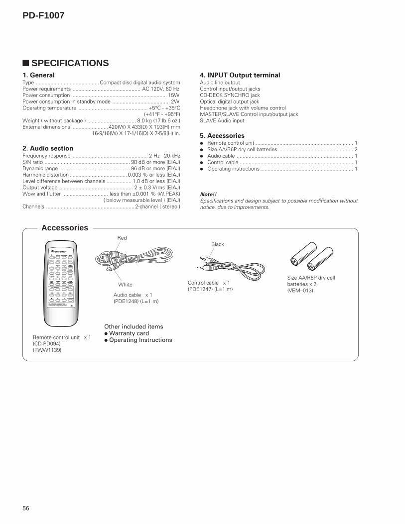
5. Accessories÷ Remote control unit .................................................................. 1÷ Size AA/R6P dry cell batteries ................................................... 2÷ Audio cable ............................................................................... 1÷ Control cable ............................................................................. 1÷ Operating instructions ............................................................... 1
Note!!
Specifications and design subject to possible modification withoutnotice, due to improvements.
1. GeneralType ...........................................Compact disc digital audio systemPower requirements .............................................. AC 120V, 60 HzPower consumption ................................................................. 15WPower consumption in standby mode ....................................... 2WOperating temperature ............................................... +5°C - +35°C
(+41°F - +95°F)Weight ( without package ) ................................. 8.0 kg (17 lb 6 oz.)External dimensions ......................... 420(W) X 433(D) X 193(H) mm
16-9/16(W) X 17-1/16(D) X 7-5/8(H) in.
2. Audio sectionFrequency response ................................................... 2 Hz - 20 kHzS/N ratio .......................................................... 98 dB or more (EIAJ)Dynamic range ................................................ 96 dB or more (EIAJ)Harmonic distortion ....................................... 0.003 % or less (EIAJ)Level difference between channels ................. 1.0 dB or less (EIAJ)Output voltage .................................................. 2 ± 0.3 Vrms (EIAJ)Wow and flutter ............................... less than ±0.001 % (W.PEAK)