14
Filed Effect Transistors (FETs) Chapter 7
| Date post: | 19-Dec-2015 |
| Category: |
Documents |
| View: | 225 times |
| Download: | 0 times |

Filed Effect Transistors (FETs)
Chapter 7

JFET

VGS Effect
G-S junction is reverse-biased with negative voltage (VG) depletion region
VG less than zero VG controls the drain current, ID
Higher VG narrows the channel Larger depleted region
– Larger barrier voltage larger resistance less current through ID
Less VG wider channel larger ID
Note: In this case VGG = VGS

N and P-type JFETs
N-type – VDD>= 0– VGS<=0– VGS(cutoff) < 0; ID=0
P-type– VDD<= 0– VGS>=0– VGS(cutoff) > 0; ID=0

Drain Characteristic: VDS-ID Curve
VGS is shorted VGS=0 IDSS is the maximum drain
current allowed at the Vp (Pinch-off voltage)
ID is proportional to VDD Constant chan. Resistance
(ohmic area)ID is almost
constant(constant current-
area)
VGD – reverse biased voltage causes large
depletion area Very narrow
channel Fast change of ID due
to VDS - breakdown

Drain Characteristic Curves
VGS = [0 to -5] VGS = -5 cutoff voltage ID is almost zero
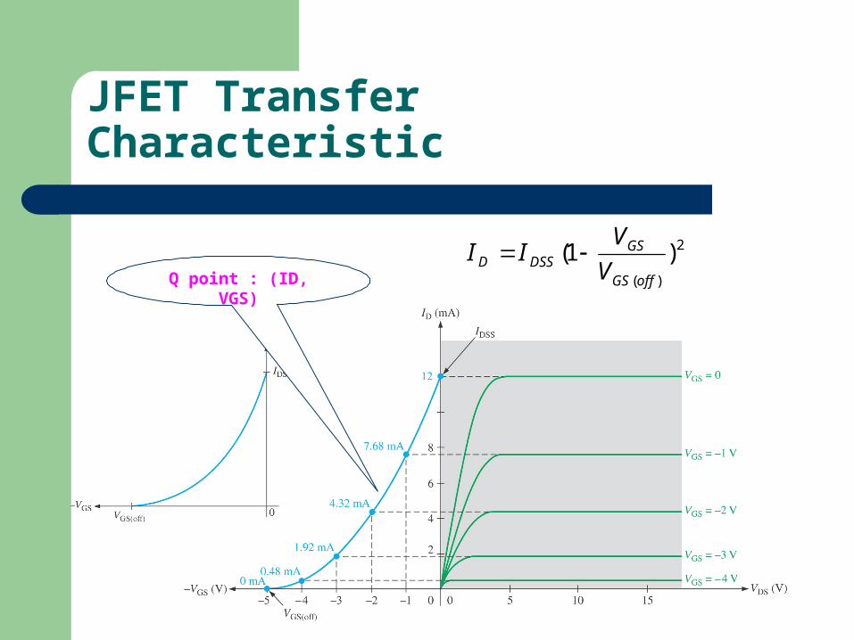
JFET Transfer Characteristic
Q point : (ID, VGS)
2
)(
)1(offGS
GSDSSD V
VII

JFET Transfer Characteristic
Self-biased DC Load Line
VGS is zero; Remember: For self-biased dc
load line VGS=ID x RS
Self-Biased---------------VGS=-ID x RS
2
)(
)1(offGS
GSDSSD V
VII
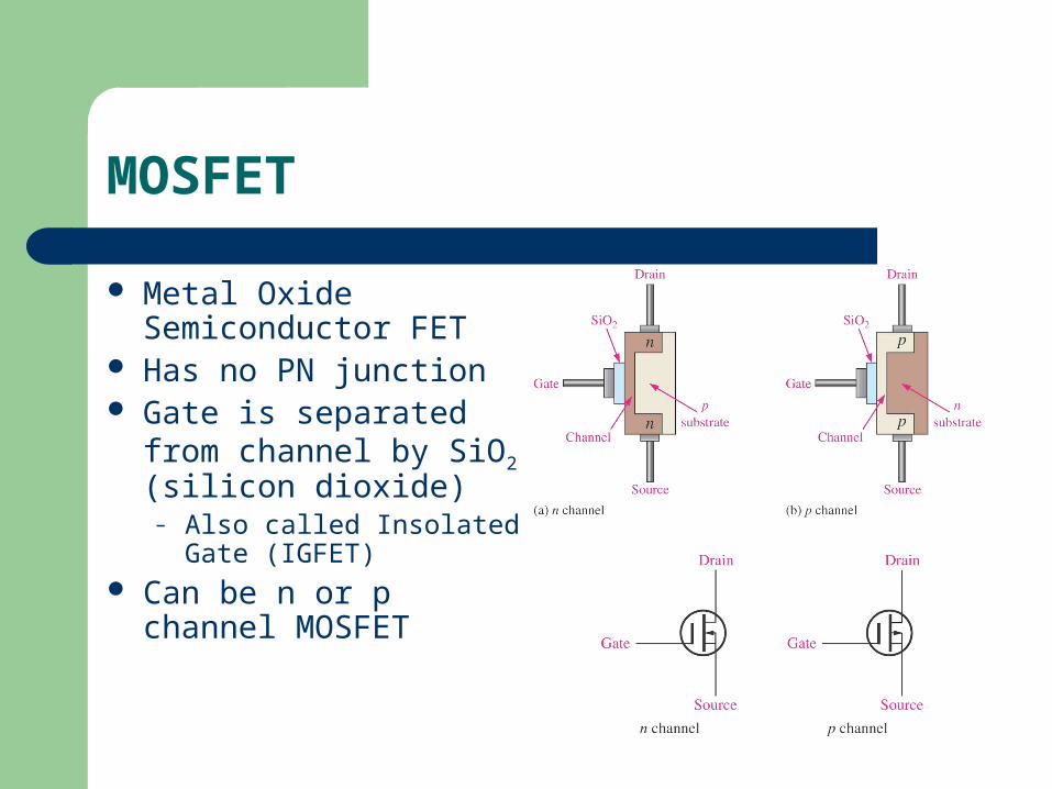
MOSFET
Metal Oxide Semiconductor FET
Has no PN junction Gate is separated from
channel by SiO2 (silicon dioxide)
– Also called Insolated Gate (IGFET)
Can be n or p channel MOSFET

D-MOSFET
P-type and n-type have different voltage polarities
The gate voltage can be positive or negative Two modes of operations:
– Depletion (VGS<0)– Enhancement (VGS>0)

E-MOSFET
P-type and n-type have different voltage polarities
Operates only in Enhancement Mode– If n-type VGS >0 – If p-type VGS <0
NOTE: The channel is closed until voltage is applied to the gate:
VGS>VGS(TH)

Transfer Characteristic Curves
D-MOSFETE-MOSFET
Parabolic Curve
2)( )( THGSGSD VVKI
2
)(
)1(offGS
GSDSSD V
VII
2)(
)(
)( THGSGS
OND
Vv
IK
VGS(TH) and ID(ON) can be found from the data sheet
VSG
ID

For more information click on each topic:
Transistor, bipolar, NPN
Transistor, bipolar, PNP
Transistor, Junction FET, N-channel
Transistor, Junction FET, P-channel
Transistor, MOSFET, N-channel, depletion mode
Transistor, MOSFET, N-channel, enhancement mode
Transistor, MOSFET, P-channel, depletion mode
Transistor, MOSFET, P-channel, enhancement mode
Know the symbols!

JFET Transfer Characteristic
ID = IDSS (1 – VGS/VGF(off) ) 2
Load Line
VGS is15; Remember: Voltage
divider-biased; slot is VG/Rs
Voltage-Divider- Biased---------------VS=ID x RSVG=VDD(R2/RT)VGS=VG-VS


