Page 1
Fin and Island Isolation of AlGaN/GaN HFETs and
Temperature-dependent Modeling of Drain Current
Characteristics of AlGaN/GaN HFETs
Bandar AlOtaibi
A Thesis
in
The Department
of
Electrical and Computer Engineering
Presented in Partial Fulfillment of the Requirements
for the Degree of Master of Applied Science (Electrical Engineering) at
Concordia University
Montreal, Quebec, Canada
June 2011
© Bandar AlOtaibi, 2011
Page 2
CONCORDIA UNIVERSITY
SCHOOL OF GRADUATE STUDIES
This is to certify that the thesis prepared
By: Bandar Al-Otaibi
Entitled: ―Fin and Island Isolation of AlGaN/GaN HFETs and Temperature-
dependent Modeling of Drain Current Characteristics of AlGaN/GaN
HFETs‖
and submitted in partial fulfillment of the requirements for the degree of
Master of Applied Science
Complies with the regulations of this University and meets the accepted standards with
respect to originality and quality.
Signed by the final examining committee:
________________________________________________ Chair
Dr. R. Raut
________________________________________________ Examiner, External
Dr. M. Packirisamy (MIE) To the Program
________________________________________________ Examiner
Dr. M. Z. Kabir
________________________________________________ Supervisor
Dr. P. Valizadeh
Approved by: ___________________________________________
Dr. W. E. Lynch, Chair
Department of Electrical and Computer Engineering
____________20_____ ___________________________________
Dr. Robin A. L. Drew
Dean, Faculty of Engineering and
Computer Science
Page 3
iii
ABSTRACT
Fin and Island Isolation of AlGaN/GaN HFETs and Temperature-dependent
Modeling of Drain Current Characteristics of AlGaN/GaN HFETs
Bandar AlOtaibi
Over the past two decades AlGaN/GaN Heterostructure Field Effect Transistors (HFETs)
have been the target of many studies on their suitability for high-power and high-
temperature applications. Due to the sizable inherent polarization effects, present in these
heterostructure-based devices, the built-in sheet charge density at the AlGaN/GaN
heterointerface is remarkably high, which makes these devices fall into the category of
the depletion-mode field effect transistors. Despite the suitability of this wide-bandgap
material system for switching power applications, the depletion-mode character of these
HFETs has been acting as an obstacle against the adoption of AlGaN/GaN HFETs to
these applications. As a result, a vibrant research on the development of techniques
capable of reliably changing the depletion-mode character of AlGaN/GaN HFETs into an
enhancement-mode character is currently being pursued by many investigators. Towards
this end, the proposed approach of this thesis has been based on modifying the
piezoelectric component of the polarization sheet charge density through studying its
correlation with the size of the isolation mesa.
The impact of the size of the isolation-mesa on the sweeping- and pulsed-mode drain
current-voltage characteristics of AlGaN/GaN HFETs has been studied. Investigations
reveal that while by implementing AlGaN/GaN HFETs on array of islands or mesas of
smaller dimensions, rather than one continuous-mesa, same values for the maximum
drain current level can be maintained, pinch-off voltage can be made less negative. Also,
Page 4
iv
it is shown that the maximum gate transconductance is improved by island-type isolation.
In addition, it is shown that the proportionally larger surface area available for power
dissipation in fin- and island-isolated HFETs can reduce the impact of self-heating on
AlGaN/GaN HFETs.
Modeling the drain current of AlGaN/GaN HFETs at high-temperature ambient
was also another objective of this thesis. A Monte Carlo-based temperature-dependent
mobility model, with incorporation of steady-state velocity overshoot, is employed in
modeling the drain current-voltage characteristics of AlGaN/GaN HFETs at 300, 400,
and 500K. One of the major merits of this model is that it employs a very small set of
fitting parameters. The model takes into account the temperature-dependence of the
electron transport through the gated-channel of an AlGaN/GaN HFET and also its access
regions. This model is validated with regards to the experimentally measured drain
current characteristics. Results confirm that the temperature dependency of the drift
electron velocity is the cause of the degradation of drain current at elevated temperatures.
Page 5
v
AKNOWLEDGEMENTS
I would like to thank, first of all, Professor Pouya Valizadeh to whom I owe a great debt.
It is certainly a great privilege for me to have worked under his supervision. His share of
knowledge, his wisdom, and supportive character are the assets on which this work has
been framed. During these years, he guided me through the field of III-Nitride
electronics. I will regret missing his inspiring talks.
I would like to thank Professor Mojtaba Kahrizi for making his laboratory and
characterizing instruments accessible. Also, I would like to show my gratitude to
Professor M. Zahangir Kabir for his lectures and impressive mathematical reasoning,
which encouraged me to learn more about quantum mechanics and Nano-devices. I thank
also Professor Sheldon Williamson for his previous supervision of an interesting power-
electronic project, his kindness, and also for greeting me in Arabic. Also, I take this
opportunity to thank Dr. Imed Zine-El-Abidine from Canadian Microelectronics
Corporation (CMC) for his useful discussions.
Special thanks go to my father and my mother, from whom I get endless
encouragement and passion. Their support and their devotion to me kept me going. I
thank my brothers and sisters for their care and support.
I would like to thank also my colleagues and group mates: Mr. Farzin
Manouchehri, Mr. Hassan Algharni, Mr. Maziar Moradi, and Mr. Alireza Loghmany.
They made of such stressful work area an enjoyable and delightful atmosphere.
I give my special gratitude to my wife and to my two beloved angels: Zaid and
Auroob. Their compromises and sacrifices are the key factors to my accomplishments.
Page 6
vi
I gratefully acknowledge the support of King Abdullah Foreign Scholarship
Program.
I acknowledge also the Canadian Microelectronics Corporation (CMC) for the
microfabrication of the devices and also the Discovery Grant Program of the Natural
Sciences and Engineering Research Council of Canada (NSERC) for supporting this
work through a grant to my supervisor Professor Pouya Valizadeh.
Page 7
vii
Table of Contents
List of Figures ................................................................................................................... ix
List of Tables .................................................................................................................... xi
1 Introduction ..................................................................................................................1
1.1 Material properties of III-Nitride .............................................................. 1
1.2 Spontaneous polarization in GaN ...........................................................................3
1.3 AlGaN/GaN Heterostructure Field-Effect Transistor ............................................4
1.3.1 Polarization engineering in AlGaN/GaN HFETs ..........................................7
1.3.2 Performance of AlGaN/GaN HFETs in high-temperature ambient ..............9
1.4 Overview of thesis ................................................................................................10
2 Fin and Island Isolation of AlGaN/GaN HFETs ....................................................11 2.1 Abstract ...............................................................................................................11
2.2 Introduction .........................................................................................................12
2.3 Fabrication techniques for enhancement-mode AlGaN/GaN HFETs ..................13
2.4 Experimental results and discussion ....................................................................16
2.4.1 Device structure and characterization ........................................................16
2.4.2 Discussion ..................................................................................................21
2.5 Conclusion ...........................................................................................................24
3 Investigation of the Impact of Temperature Dependency of Drift Transport
Characteristics on the Drain Current of AlGaN/GaN HEFTs .............................25 3.1 Abstract.................................................................................................................25
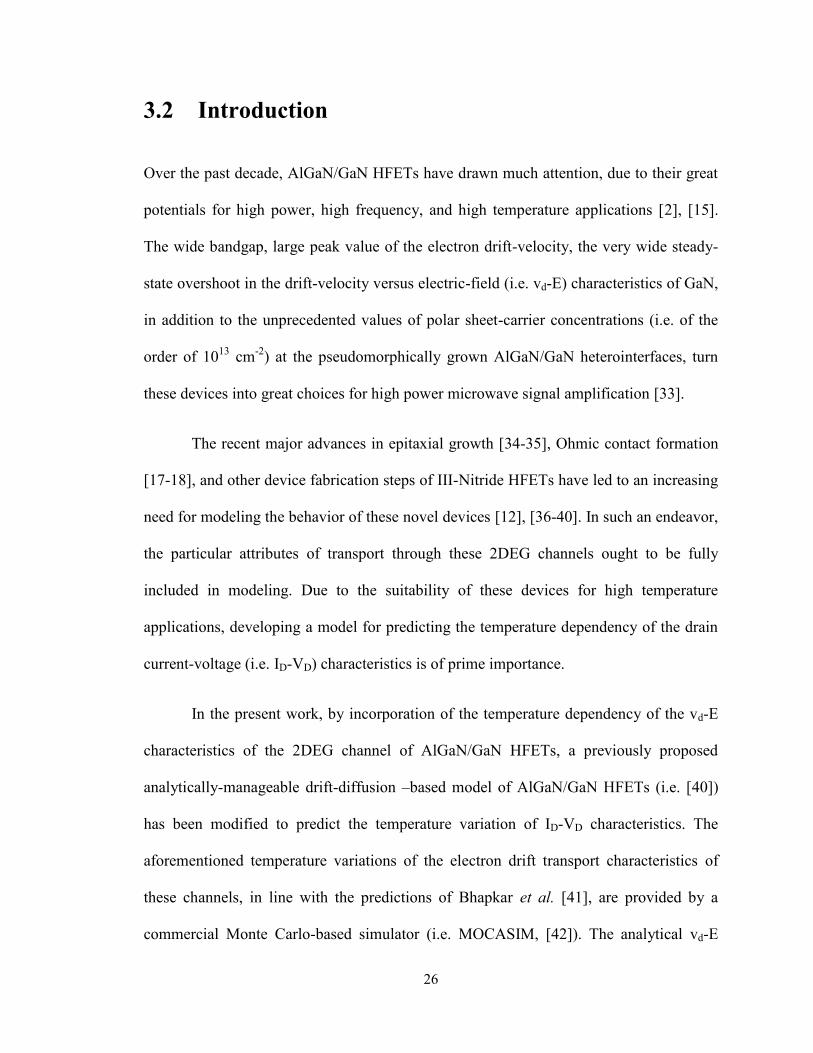
3.2 Introduction ..........................................................................................................26
3.3 Temperature Dependency of vd-E Characteristics ...............................................27
3.4 Drain-current modeling of AlGaN/GaN HFETs ..................................................31
3.4.1 Linear Regime ...............................................................................................32
3.4.2 Saturation Regime .........................................................................................33
3.4.3 Temperature variations of the channel potential ..........................................36
3.5 Experimental Background and Discussions.......................................................37
3.5.1 Assessment of the temperature-dependent device model ............................40
3.5.2 Role of the accurate modeling of high-field drift- velocity in high-
temperature device modeling .................................................................................44
3.6 Conclusion ........................................................................................................51
Page 8
viii
4 Conclusion and Future Works .................................................................................52
Bibliography .....................................................................................................................55
Page 9
ix
LIST OF FIGURES
Figure 1.1: Electron drift transport characteristics of Si, SiC, GaAs, and GaN [6]. ............2
Figure 1.2: A stick-and-ball diagram of hexagonal crystalline structure of GaN in Ga-
face and N-face [4]. ............................................................................................3
Figure 1.3: Schematic drawing of the conduction band structure of AlGaN/GaN
HFET..................................................................................................................6
Figure 1.4: Spontaneous and piezoelectric polarization in AlGaN/GaN HFET [11] ..........7
Figure 1.5: Schematic drawing of the basic structure of an AlGaN/GaN HFET ................7
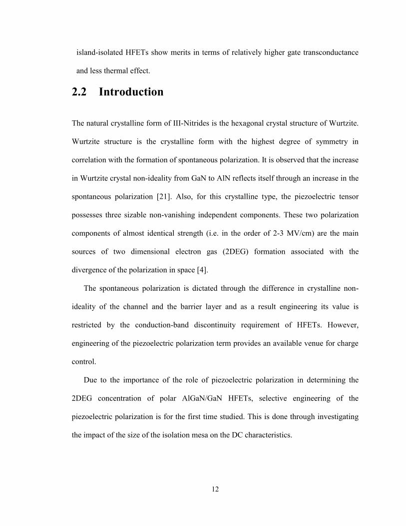
Figure 2.1: Formation of peel forces at the edges of a tensile strained thin film...............15
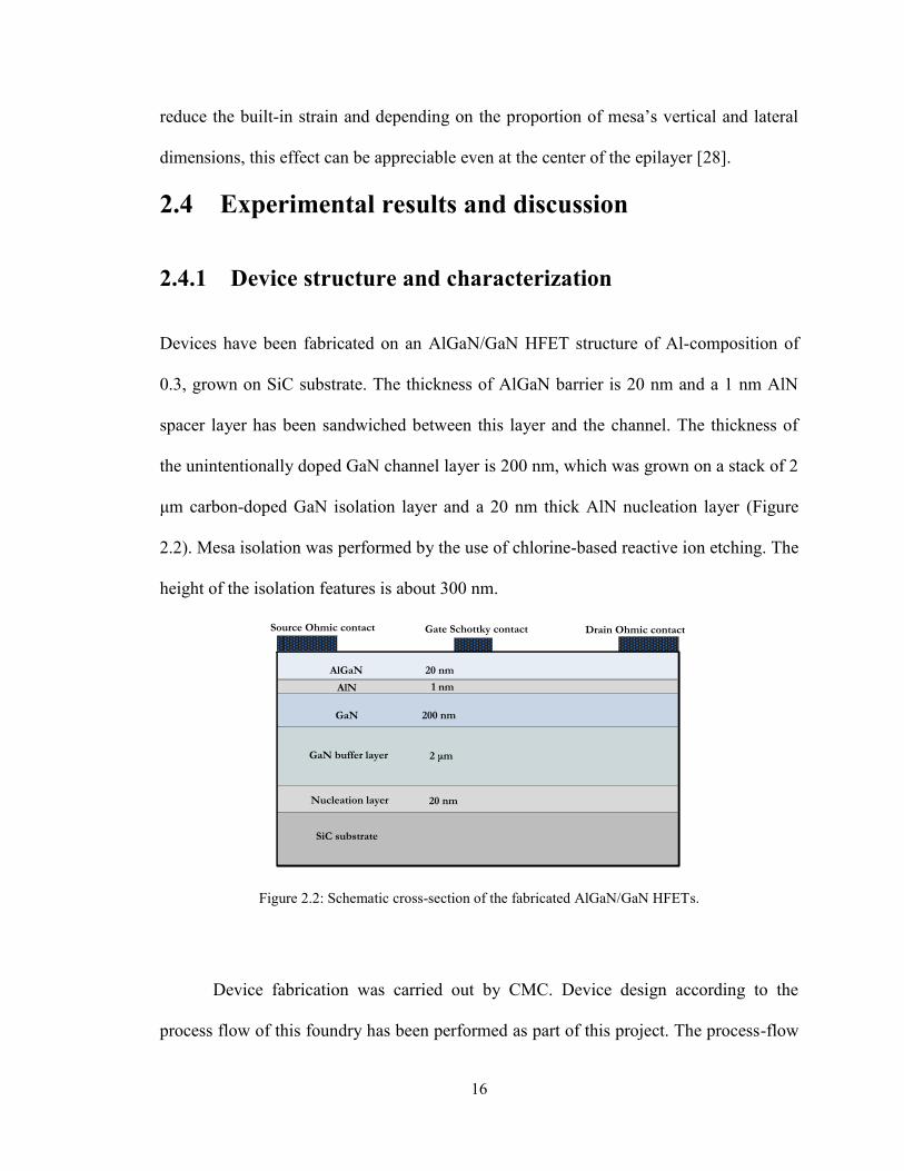
Figure 2.2: Schematic cross-section of the fabricated AlGaN/GaN HFETs... ..................16
Figure 2.3: Device layout of a two-finger fin-isolated AlGaN/GaN HFET with micro-
strip interconnects ............................................................................................18
Figure 2.4: Device layout of a two-finger island-isolated AlGaN/GaN HFET with
micro-strip interconnects .................................................................................19
Figure 2.5: Micrographs of the fin-isolated HFET (a), and the island-isolated HFET
(b) .....................................................................................................................20
Figure 2.6: Scaled extrinsic gate transconductance versus gate-source voltage for
mesa- (continuous), fin- (dashed), and island-isolated (dotted) devices.
VDS is equal to 5V. ...........................................................................................21
Figure 2.7: Scatter plot of the variation of the pinch-off voltage among the three
categories of devices ........................................................................................22
Figure 2.8: Scaled drain- and gate-current versus drain-source voltage, for a typical
mesa-isolated HFET (a), fin-isolated HFET (b), and island-isolated HFET
(c). On all these figures pulsed drain current values are indicated in dashed
lines. VGS is changed from -5 to 0 V, in steps of 0.5 V... ................................23
Figure 3.1: Electron drift transport characteristics of GaN at 300, 400, and 500K from
MOCASIM ......................................................................................................28
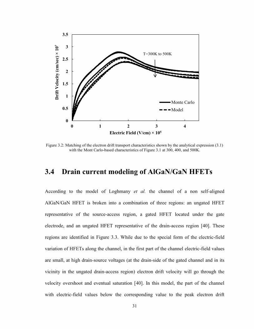
Figure 3.2: Matching of the electron drift transport characteristics shown by the
analytical expression (3.1) with the Mont Carlo-based characteristics of
Figure 3.1 at 300, 400, and 500K.....................................................................31
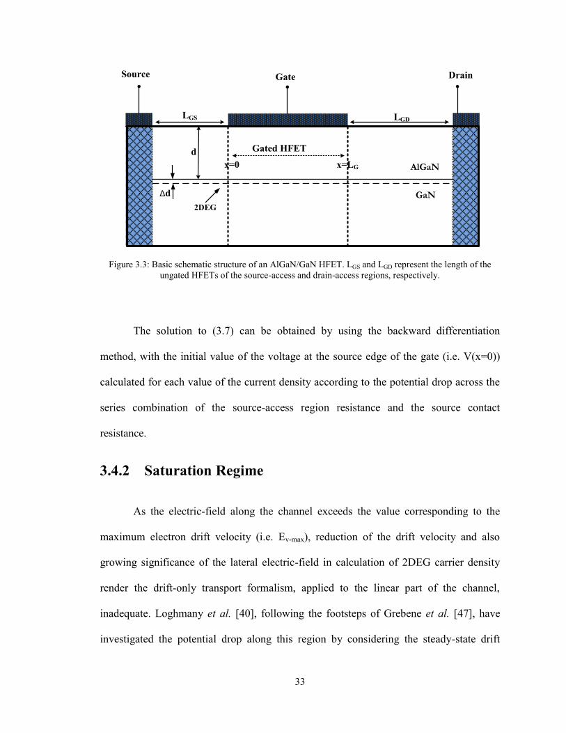
Figure 3.3: Basic schematic structure of an AlGaN/GaN HFET. LGS and LGD
represent the length of the ungated HFETs of the source-access and drain-
access regions, respectively .............................................................................33
Page 10
x
Figure 3.4: Schematic illustration of the boundaries of the Gaussian box formed in the
saturation region. The conduction band edge of AlGaN/GaN
heterointerface is shown in the inset ................................................................35
Figure 3.5: ID-VG characteristics when VD=1V at T=300 through 500K, in step of
50K ...................................................................................................................37
Figure 3.6: Device layout of a two-finger AlGaN/GaN HFET with micro-strip
interconnects.. ..................................................................................................39
Figure 3.7: ID-VD characteristics based on model (solid line) and experimental results
(dashed line) at T=300K for VG=-3 to -1V, in step of 0.5V.. ..........................41
Figure 3.8: Convergence of electric-field (a), channel-potential distribution (b),
effective threshold-voltage (c), linear electron mobility (d), electron drift
velocity (e), sheet charge density distribution (f), diffusion current density
(g), and drift current density (h) at VG=-3 V and current density equal to
1.378 A/cm at T=300K where final results are shown in solid line, initial
guesses for electric-field, channel potential, and effective threshold
voltage in dashed lines, and iterations are shown in dotted line.. ...................42
Figure 3.9: ID-VD characteristics based on model (solid line) and experimental results
(dashed line) at T=400 (a), and 500K (b), for VG=-3 to -1V in step of
0.5V. The temperature variation of the sheet resistance in the access
region is fully considered.. ...............................................................................43
Figure 3.10: ID-VD characteristics based on model (solid line) and experimental
results (dashed line) at T=400 (a), and 500K (b), for VG=-3 to -1V in step
of 0.5V. The temperature variation of the sheet resistance in the access
region is not considered.. .................................................................................44
Figure 3.11: Matching of the electron drift transport characteristics shown by the
analytical expression (3.1) with the Mont Carlo-based characteristics of
Figure 3.1 at 300, 400, and 500K, according to the transport model (1) and
(2), respectively shown in (a) and (b) .............................................................47
Figure 3.12: ID-VD characteristics based on the transport model (1) (solid line) and
experimental results (dashed line) at T=400 (a), and 500K (b), for VG=-3
to -1V in step of 0.5V ......................................................................................48
Figure 3.13: ID-VD characteristics based on the transport model (2) (solid line) and
experimental results (dashed line) at T=400 (a), and 500K (b), for VG=-3
to -1V in step of 0.5V ......................................................................................49
Page 11
xi
LIST OF TABLES
Table 1.1: Comparison of material properties between GaN, Si, GaAs, and SiC at 300K
[7] .....................................................................................................................2
Table 3.1: Model parameters of (3.1) at 300K................................................................29
Table 3.2: Device parameters and parameters used in the model ..................................39
Table 3.3: Current density at the onset of saturation and saturation current density at
300K ...............................................................................................................50
Table 3.4: Current density at the onset of saturation and saturation current density at
400K ..............................................................................................................50
Table 3.5: Current density at the onset of saturation and saturation current density at
500K ..............................................................................................................50
Page 12
1
Chapter 1
Introduction
1.1 Material properties of III-Nitride
III-Nitride semiconductors (i.e. InN, GaN, AlN, and their ternary alloys) are promising
candidates for many high-power, high-frequency, and high-temperature electronic
applications [1-2]. This is a consequence of their wide bandgap, large peak value of the
electron drift-velocity, the very wide steady-state overshoot in the drift-velocity versus
electric-field (i.e. vd-E) characteristics, and high breakdown electric-field. Additionally,
the widely tuneable bandgap of ternary III-Nitride alloys can cover a very broad range of
absorption and emission characteristic wave-lengths from infrared to the ultraviolet,
which make them superb choices for electronic and optoelectronic devices (e.g. light
emitting diodes, laser diodes, and photo detectors) [3].
Due to the polar nature of III-Nitride heterostructures, two-dimensional channels
of extremely high carrier concentrations (i.e. of the order of 1013
cm-2
) are formed at the
III-Nitride heterointerfaces, without the need for any intentional doping [4]. The drift-
velocity versus electric-field characteristics of GaN, not unlike other III-V
semiconductors, is shown to possess an overshoot at moderate values of electric-field and
a saturating characteristic at higher electric-fields. However, this overshoot pattern is
remarkably wider and taller than that of the other III-V semiconductors of interest. The
large peak electron velocity, wide velocity overshoot, and thermal stability of GaN have
Page 13
2
favoured GaN over GaAs, especially at lower microwave frequency and higher power
applications [4-5]. Figure 1.1 shows a comparison of electron drift-velocity versus
electric-field characteristics of GaN with three other major semiconductors (i.e. Si, GaAs,
and SiC) [6].
Figure 1.1: Electron drift transport characteristics of Si, SiC, GaAs, and GaN [6].
Among the major semiconductors presented in Figure 1.1, GaN has the widest
energy bandgap and the highest breakdown electric-field. This makes this semiconductor
very suitable for the channel of high voltage FETs. Table 1.1 compares the bandgap
energy, electron mobility (μn), breakdown field (Eb), and electron saturation velocity (vsat)
of GaN to these other major semiconductors. Although GaN has a considerably lower
electron mobility than GaAs, its higher and wider steady-state velocity overshoot and
higher saturation velocity serve as compensating factors towards providing competitive
current density and power gain at moderate frequencies.
Table 1.1: Comparison of material properties between GaN, Si, GaAs, and SiC at 300K [7].
Material Si GaAs 4H-SiC GaN
Eg (eV) 1.1 1.42 3.26 3.39
µn (cm2/Vs) 1350 8500 700 900
Eb (106 V/cm) 0.3 0.4 3 3.3
vsat (107 cm/s) 1.0 2.0 2.0 2.5
Page 14
3
1.2 Spontaneous polarization in GaN
III-Nitride semiconductors can be grown in two different crystalline forms: Zinc blende
(Zb) and Wurtzite (Wz) [5]. The Wurtzite structure, which has a hexagonal unit cell, is
the most studied form of III-Nitrides. This is due to the extraordinary polar properties of
III-Nitrides in this crystalline form. Due to the non-centrosymmetric nature of these
Wurtzite crystals, a very large spontaneous polarization is built into the as grown crystal.
The value of the spontaneous polarization of GaN is in the order of 3MV/cm [8].
Improvement of such a large component of the spontaneous polarization in the
Wurtzite crystals of III-Nitrides is observed along the material order of GaN to InN, and
to AlN [8].
Figure 1.2: A stick-and-ball diagram of hexagonal crystalline structure of GaN in Ga-face and N-
face [4].
The growth technique of GaN has been found to bear the possibly of determining
the direction of the aforementioned spontaneous polarization vector [4]. This direction is
dependent on the face of the grown crystal. Due to the lack of lattice-matched substrates,
Page 15
4
III-Nitrides are often grown on c-plane Sapphire or SiC substrates. The crystal can either
be grown in metallic-face (which is also known as Ga-face) or N-face. As shown in
Figure 1.2, the face of the crystal is determined by the type of the atoms of which the
topmost layer of the grown crystal is composed. Using the MOVPE (Metal Organic
Vapor Phase Epitaxy) growth technique, the Ga-face is observed to be the dominant face
[4]. The direction of the spontaneous polarization vector of Ga-face III-Nitride crystals
points toward the substrate, while perpendicular to it. In the N-face crystals, spontaneous
polarization vector points toward the surface [4].
1.3 AlGaN/GaN Heterostructure Field Effect
Transistor (HFET)
In HFETs, the barrier layer, which separates the gate electrode from the channel, is often
composed of a wide-bandgap semiconductor (i.e. AlGaN in the case of AlGaN/GaN
HFET). The conduction band bending at the heterointerface between the wide-bandgap
barrier layer, and the smaller bandgap channel layer results in the formation of a two
dimensional electron gas (i.e. 2DEG) at the triangular quantum well, created at the
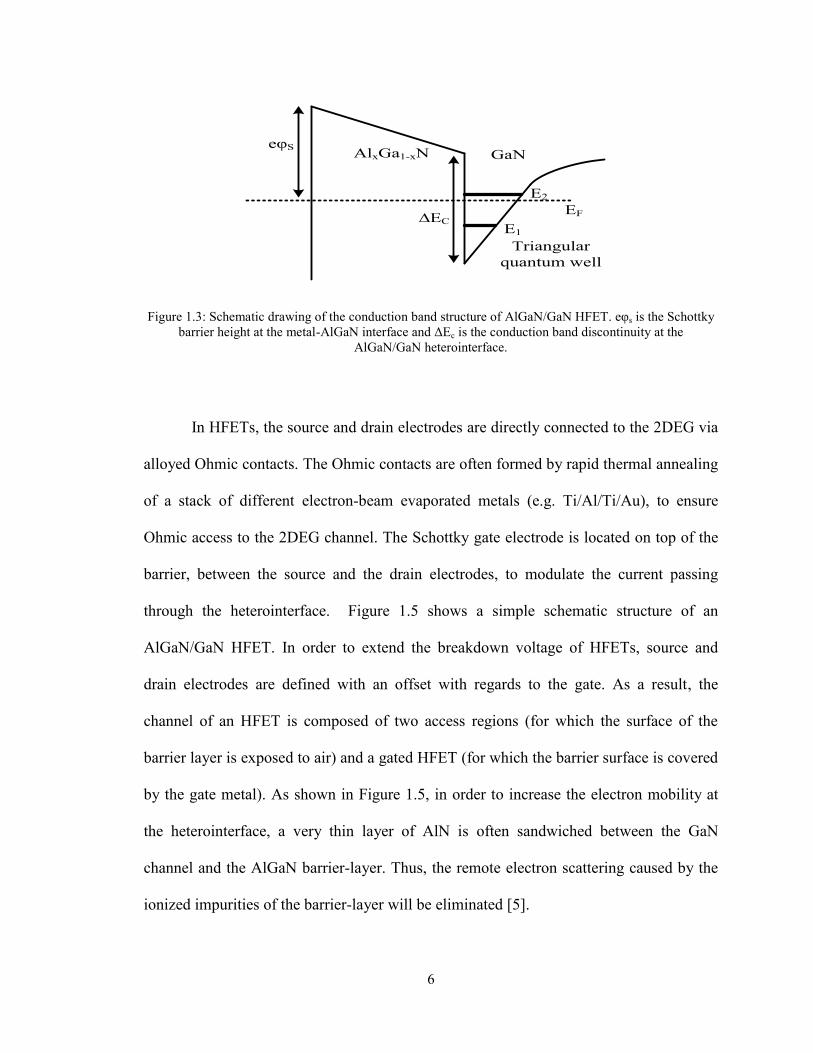
channel-side of the interface (i.e. GaN-side). This is illustrated in Figure 1.3. In this
figure, E1 and E2 represent the first and second subbands of the triangular quantum well.
The flow-path of the drain current of a properly designed HFET is restricted to this
quantum well.
In non-polar HFETs, the 2DEG is formed by the transfer of electrons from the
intentionally doped barrier to the triangular quantum well. In contrast, the 2DEG of polar
Page 16
5
III-Nitride HFETs is formed dominantly due to the polar nature of the AlGaN/GaN
heterointerface. The induction of the polarization charge at this heterointerface is partly
the result of the mismatch of the spontaneous polarization of the barrier and the channel
layer. These two layers despite the uniqueness of the direction of their polarization
vectors have different values of polarization. As a result of the polarization imbalance at
the heterointerface, formation of the 2DEG at the GaN-side of the heterointerface will
become necessary [9-10]. This polar 2DEG is observed to form even in the absence of
intentional doping of the barrier.
In addition to the polarization induced at the heterointerface by the discontinuity
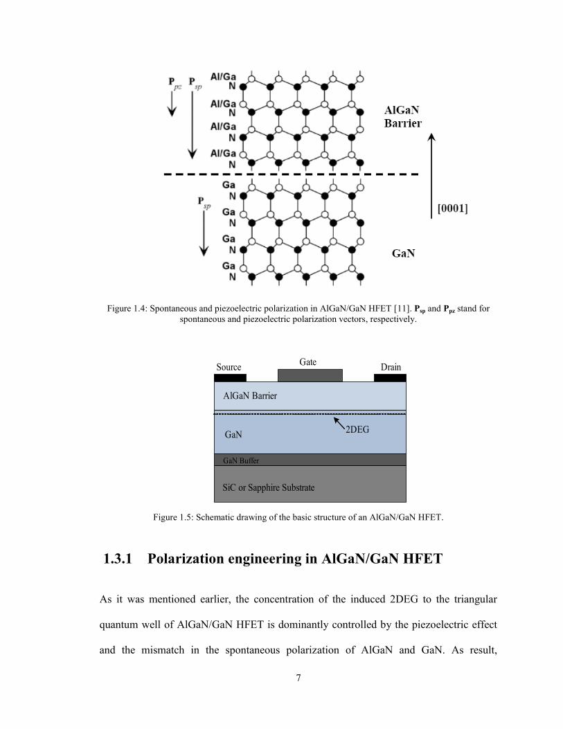
of the spontaneous polarization of GaN and AlGaN, the lattice mismatch of the barrier
and the channel layer is the cause of another polarization component. Due to the smaller
value of the lateral lattice constant of AlGaN in comparison to GaN, pseudomorphic
growth of AlGaN on top of GaN results in induction of tensile strain at the AlGaN/GaN
heterointerface. As a result of this induced strain and existence of large off-diagonal
elements in the strain tensor of III-Nitrides, piezoelectric polarization to the extent
comparable to the spontaneous polarization, and of the same direction, will be formed at
the AlGaN/GaN heterointerface [4]. This is shown in Figure 1.4. The combined impact of
the piezoelectric effect and the spontaneous polarization results in formation of 2DEG
with densities exceeding 1013
cm-2
.
Page 17
6
EF
E1
E2
Triangular
quantum well
AlxGa1-xN GaNeφS
∆EC
Figure 1.3: Schematic drawing of the conduction band structure of AlGaN/GaN HFET. eφs is the Schottky
barrier height at the metal-AlGaN interface and ΔEc is the conduction band discontinuity at the
AlGaN/GaN heterointerface.
In HFETs, the source and drain electrodes are directly connected to the 2DEG via
alloyed Ohmic contacts. The Ohmic contacts are often formed by rapid thermal annealing
of a stack of different electron-beam evaporated metals (e.g. Ti/Al/Ti/Au), to ensure
Ohmic access to the 2DEG channel. The Schottky gate electrode is located on top of the
barrier, between the source and the drain electrodes, to modulate the current passing
through the heterointerface. Figure 1.5 shows a simple schematic structure of an
AlGaN/GaN HFET. In order to extend the breakdown voltage of HFETs, source and
drain electrodes are defined with an offset with regards to the gate. As a result, the
channel of an HFET is composed of two access regions (for which the surface of the
barrier layer is exposed to air) and a gated HFET (for which the barrier surface is covered
by the gate metal). As shown in Figure 1.5, in order to increase the electron mobility at
the heterointerface, a very thin layer of AlN is often sandwiched between the GaN
channel and the AlGaN barrier-layer. Thus, the remote electron scattering caused by the
ionized impurities of the barrier-layer will be eliminated [5].
Page 18
7
Figure 1.4: Spontaneous and piezoelectric polarization in AlGaN/GaN HFET [11]. Psp and Ppz stand for
spontaneous and piezoelectric polarization vectors, respectively.
SourceGate
Drain
AlGaN Barrier
GaN
SiC or Sapphire Substrate
GaN Buffer
2DEG
Figure 1.5: Schematic drawing of the basic structure of an AlGaN/GaN HFET.
1.3.1 Polarization engineering in AlGaN/GaN HFET
As it was mentioned earlier, the concentration of the induced 2DEG to the triangular
quantum well of AlGaN/GaN HFET is dominantly controlled by the piezoelectric effect
and the mismatch in the spontaneous polarization of AlGaN and GaN. As result,
Page 19
8
engineering these components of inherent polarization are the dominant factors in
controlling the 2DEG concentration and current-drive of AlGaN/GaN HFETs. These
factors are also invaluable in exerting control over the threshold voltage of AlGaN/GaN
HFETs.
Due to the large values of 2DEG densities induced to the polar AlGaN/GaN
heterointerfaces, the threshold-voltage of these devices is often negative, resulting in
realization of depletion-mode (or, normally-on) FETs. However, in many applications the
presence of normally-on devices results in insupportable energy expenditure in the
standby mode. As a result, an ongoing research is being pursued in terms of producing
Enhancement-mode (or, normally-off) AlGaN/GaN HFETs with positive values of
threshold voltage, or even devices of less-negative values of threshold-voltage.
As a result of the dominance of the polarization fields in defining the 2DEG
concentration of AlGaN/GaN HFETs, the required level of control exerted towards
positive-shifting of the threshold-voltage is expected to be realizable by means of
engineering the polarization. While both spontaneous and piezoelectric polarizations can
be reduced by reducing the Al-composition of the AlGaN barrier (and essentially
bringing the material properties of the channel and the barrier layer more towards one
another), such an HFET design will heavily suffer in terms of the gate leakage current
through the low Al-composition AlxGa1-xN barrier layer. As a result, other avenues of
engineering the polarization are pursued in Chapter 2 of this thesis.
Page 20
9
1.3.2 Performance of AlGaN/GaN HFETs in high-
temperature ambient
The low generation rate of thermally-induced carriers and the high thermal conductivity
of GaN and AlGaN, turn AlGaN/GaN HFETs to suitable transistors for high-temperature
applications (e.g. in automotive, aircraft, and aerospace applications) [12-15]. It should
also be mentioned that AlGaN/GaN HFETs have shown considerable thermal stability. In
addition, it is known that the steady-state velocity overshoot and the saturation electron
drift velocity of GaN are less affected by the temperature increase in comparison with
GaAs [16]. Adding to these suitable material characteristics, the recent developments of
techniques of Ohmic contact formation and surface treatments of AlGaN/GaN HFETs
have also led to substantial improvements in the high-temperature reliability of these
contacts [17-18].
AlGaN/GaN HFETs fabricated on SiC substrates show greater potential in terms
of thermal stability, due to the high thermal conductivity of SiC [19]. It is shown that
low-field electron mobility of the 2DEG is enhanced by the higher thermal conductivity
of the Si substrate in comparison to Sapphire (which is the other widely used substrate in
AlGaN/GaN technology) [20].
The aforementioned factors lead to the popularity of AlGaN/GaN HFETs for
high-temperature applications. In addition, AlGaN/GaN HFETs fabricated on SiC
substrates can be integrated on-chip with the other high-temperature integrated systems.
As a result, developing a model for predicting the temperature dependency of the drain
Page 21
10
current-voltage (i.e. ID-VD) characteristics of these devices is of prime importance in
improvising better device design strategies. This is done in Chapter 3.
1.4 Overview of thesis
In Chapter 2 of the thesis a novel design strategy based on engineering the piezoelectric
polarization at the AlGaN/GaN heterointerface is proposed and experimentally
investigated. Preliminary results of this investigation show that the proposed strain
engineering technique, which is based on the application of small size isolation mesas to
the fabrication of AlGaN/GaN HFETs, bears the possibility of positive shifting the value
of the threshold-voltage.
In Chapter 3, a manageable analytical model for modeling the drain current-
voltage characteristics of AlGaN/GN HFETs at elevated temperatures is proposed and
validated with regards to the experimentally measured characteristics.
Chapter 4 includes the conclusions of this work and draws a few suggested
directions for the future work in this area.
Page 22
11
Chapter 2
Fin and Island Isolation of AlGaN/GaN
HFETs
2.1 Abstract
Traditionally AlGaN/GaN HFETs are fabricated on mesas, etched well into the
heterojunctions, to avoid the crosstalk between neighboring devices fabricated on the
same chip. In here, for the first time, effect of the size-variation of the isolation mesas of
AlGaN/GaN HFETs on their drain current characteristics is studied. In this study, the
isolation mesas of the fabricated devices include three varieties: narrow mesas (i.e.
16x40 μm2 fins), array of very small size mesas (i.e. 16x7 μm
2 islands), and
traditionally-sized mesas (i.e. 100x100 μm2). AlGaN/GaN HFETs of the
aforementioned isolation-mesa sizes are investigated in terms of their DC and pulsed
measurement characteristics. Results show a correlation between the pinch-off voltage
and the size of the isolation mesa. The pinch-off voltage is observed to become less
negative by the reduction of the size of the individual mesas. All of the fabricated
devices have peak extrinsic gate transconductance values greater than 220 mS/mm. The
Based on a paper published in May 2011 issue of the IEEE Transaction on Electron Devices.
Page 23
12
island-isolated HFETs show merits in terms of relatively higher gate transconductance
and less thermal effect.
2.2 Introduction
The natural crystalline form of III-Nitrides is the hexagonal crystal structure of Wurtzite.
Wurtzite structure is the crystalline form with the highest degree of symmetry in
correlation with the formation of spontaneous polarization. It is observed that the increase
in Wurtzite crystal non-ideality from GaN to AlN reflects itself through an increase in the
spontaneous polarization [21]. Also, for this crystalline type, the piezoelectric tensor
possesses three sizable non-vanishing independent components. These two polarization
components of almost identical strength (i.e. in the order of 2-3 MV/cm) are the main
sources of two dimensional electron gas (2DEG) formation associated with the
divergence of the polarization in space [4].
The spontaneous polarization is dictated through the difference in crystalline non-
ideality of the channel and the barrier layer and as a result engineering its value is
restricted by the conduction-band discontinuity requirement of HFETs. However,
engineering of the piezoelectric polarization term provides an available venue for charge
control.
Due to the importance of the role of piezoelectric polarization in determining the
2DEG concentration of polar AlGaN/GaN HFETs, selective engineering of the
piezoelectric polarization is for the first time studied. This is done through investigating
the impact of the size of the isolation mesa on the DC characteristics.
Page 24
13
2.3 Fabrication techniques for enhancement-mode
AlGaN/GaN HFETs
In the depletion-mode n-type FETs, the drain-current has a finite value when the gate-
source voltage is zero. As a result, for turning these devices off a negative voltage should
be applied between the gate and source electrodes. On the contrary, for an n-type
enhancement-mode FET, the flow of current occurs only when a positive gate-source
voltage is applied. In order to avoid any unnecessary power consumption in the standby
mode, enhancement-mode devices are often preferred in switching circuits. Since
AlGaN/GaN HFETs are good candidates for high-voltage applications, developing
normally-off AlGaN/GaN HFETs for high-voltage switching applications is extremely
appealing.
However, as it was discussed in Chapter 1, AlGaN/GaN HFETs due to their
extremely high values of sheet charge density fall into the depletion-mode category. Over
the years a few techniques have been proposed for the conversion of this depletion-mode
characteristic into an enhancement-mode characteristic. A few of these techniques
including ―gate-recess‖ and ―fluorine-ion bombardment‖ are briefly reviewed in this
section.
The ―gate-recess‖ technique of realization of enhancement-mode AlGaN/GaN
HFETs relies on the partial removal of the thickness of the barrier under the gate
electrode. This thinning of the barrier essentially results in depletion of the 2DEG
concentration due to the charge depleting effect of the Schottky gate. A few of the
Page 25
14
important unwanted side-effects of this process are the damage of the dry etching to the
surface of the mesa and also the increase in the gate-leakage through the thinned barrier
[22-23].
Employing fluorine-based reactive ion etching (RIE) for ―implanting fluorine
ions‖ into the barrier is the other major technique for the fabrication of enhancement-
mode AlGaN/GaN HFETs [24]. The implanted negatively charged fluorine ion
concentration in the AlGaN barrier serves to deplete the channel from the polar 2DEG
and as a result causes a positive shift in the pinch-off voltage. However, the resulting
surface damage of this bombardment process and also the chance for redistribution of
these ions under high electric-field and high-temperature operation conditions indicate
reliability concerns for this fabrication technique.
Also a less popular solution for realization of enhancement-mode AlGaN/GaN
HFETs relies on the incorporation of a p-type GaN cap layer, sandwiched between the
gate electrode and the AlGaN barrier [25]. In this technique, the positive shift achieved in
pinch-off voltage of AlGaN/GaN HFETs is the result of the formation of the depletion
region of the pn-junction under the gate electrode. The difficulty of achieving p-type
doping of GaN is one of the major hassles of this fabrication technique. These
AlGaN/GaN HFETs are also indicating large values of gate leakage current.
In this study and for the first time, a different avenue has been taken to obtain a
positive shift in the pinch-off voltage of AlGaN/GaN HFETs by the means of strain-
engineering. This technique seems to have the capacity of offering normally-on and
Page 26
15
normally-off AlGaN/GaN HFETs on the same chip without exposing the active area of
the sample to any type of reactive ion etching.
Figure 2.1: Formation of peel forces at the edges of a tensile strained thin film.
It is typically established that the pseudomorphic growth of a crystalline thin film on
a thick substrate of a different lattice constant and/or a different thermal expansion
coefficient introduces some in-plane strain. In regions apart from the edge by a distance
in the order of three times the film thickness almost all the stress lies in-plane, while a
smaller in-plane stress is developed at the edge regions [26]. The edge regions possess a
complex distribution of shear stress, which is due to transition from the free side to the
side with in-plane stress. The discontinuity of the stress at the heterojunction around the
edge region, through a phenomenon known as ―stress concentration‖, leads to an extra
force component called ―peel force‖ (Figure 2.1) [26]. The existence of the peel forces
and the reduced in-plane strain at the edge regions are expected to reduce the
piezoelectric polarization at these parts. This effect has already been investigated in other
technologies including SiGe [27-32]. In those material systems, experimental results and
theoretical calculations demonstrate that the reduction in mesa size can substantially
Substrate
Thin film (Mesa)
t
Edge region
3 x tEdge region
3 x t
Plane stress region Shear stress
Extra peel force
F=0F≠0
Substrate
Thin film (Mesa)
t
Edge region
3 x tEdge region
3 x t
Plane stress region Shear stress
Extra peel force
F=0F≠0
Page 27
16
reduce the built-in strain and depending on the proportion of mesa’s vertical and lateral
dimensions, this effect can be appreciable even at the center of the epilayer [28].
2.4 Experimental results and discussion
2.4.1 Device structure and characterization
Devices have been fabricated on an AlGaN/GaN HFET structure of Al-composition of
0.3, grown on SiC substrate. The thickness of AlGaN barrier is 20 nm and a 1 nm AlN
spacer layer has been sandwiched between this layer and the channel. The thickness of
the unintentionally doped GaN channel layer is 200 nm, which was grown on a stack of 2
μm carbon-doped GaN isolation layer and a 20 nm thick AlN nucleation layer (Figure
2.2). Mesa isolation was performed by the use of chlorine-based reactive ion etching. The
height of the isolation features is about 300 nm.
GaN
AlGaN
AlN
GaN buffer layer
Nucleation layer
SiC substrate
20 nm
1 nm
200 nm
2 μm
20 nm
Drain Ohmic contactSource Ohmic contact Gate Schottky contact
Figure 2.2: Schematic cross-section of the fabricated AlGaN/GaN HFETs.
Device fabrication was carried out by CMC. Device design according to the
process flow of this foundry has been performed as part of this project. The process-flow
Page 28
17
of the device fabrication starts with mesa isolation of 300 nm height, Ohmic contact
deposition, and rapid thermal annealing. Following these steps, interconnect deposition,
and gate-electrode deposition are carried out in this order. After this step, devices have
been passivated by a SiN film. Finally, openings through this dielectric layer have been
created for electrical access to the drain-, source-, and gate-pads.
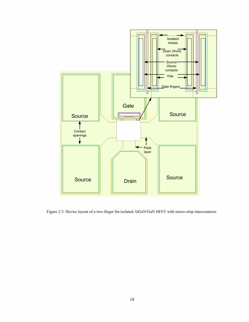
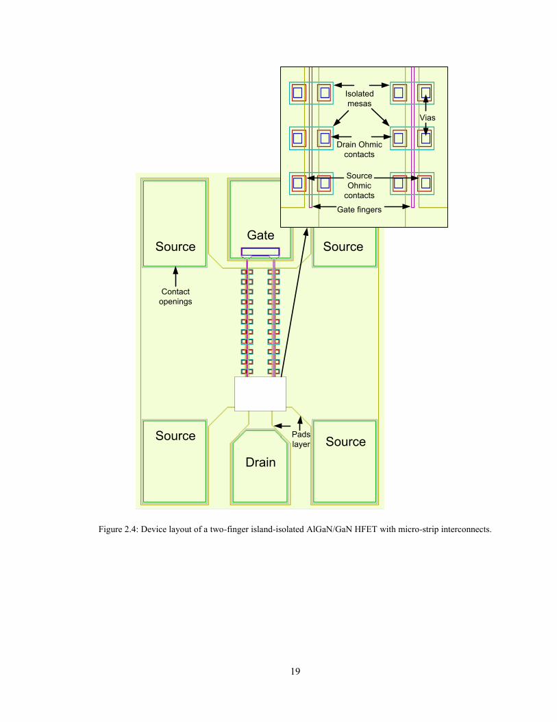
Three types of two-finger HFETs, with different sizes of isolation mesa, have
been fabricated side by side one another. The first category of devices were fabricated on
mesas of size 100x100 μm2, the second group of devices were fabricated on long small
size mesas of size 16x40 μm2, referred to as fin (Figure 2.3), and the third category of
devices were fabricated on islands of size 16x7 μm2
(Figure 2.4). As for the island type
devices, in order to maintain same value of current-drive an array of islands have been
connected together. Figure 2.5 shows micrographs of fin- and island-isolated HFETs. All
the explored devices have a gate length of 1 μm, gate-drain spacing of 2 μm, and gate-
source spacing of 1.1 μm. The Hall electron mobility of this sample was reported to be
about 1000 cm2/V.s and the 2DEG electron concentration is about 1.7x10
13 cm
-2.
Page 29
18
Source
Source
Source
SourceDrain
Gate
Isolated
mesas
Drain Ohmic
contacts
Source
Ohmic
contacts
Vias
Gate fingers
Contact
openings
Pads
layer
Figure 2.3: Device layout of a two-finger fin-isolated AlGaN/GaN HFET with micro-strip interconnects.
Page 30
19
Source
Source Source
SourceGate
Drain
Isolated
mesas
Gate fingers
Drain Ohmic
contacts
Source
Ohmic
contacts
Vias
Pads
layer
Contact
openings
Figure 2.4: Device layout of a two-finger island-isolated AlGaN/GaN HFET with micro-strip interconnects.
Page 31
20
(a)
(b)
Figure 2.5: Micrographs of the fin-isolated HFET (a), and the island-isolated HFET (b).
Page 32
21
2.4.2 Discussion
A Keithley semiconductor parameter analyzer was used for the measurements reported in
this section. Measurement results of Figure 2.6 illustrate that the pinch-off voltage
becomes less negative as the size of the mesa is reduced from 100x100 μm2
to 16x40
μm2, and to 16x7 μm
2. The maximum value of extrinsic gate-transconductance per unit-
width of the transistors remains almost the same for mesa- and fin-isolated device types.
However, wrapping the gate electrode on two sides of the islands is observed to have
increased the gate-transconductance of the island-isolated devices with respect to the
other two device types.
Figure 2.6: Scaled extrinsic gate transconductance versus gate-source voltage for mesa- (continuous), fin-
(dashed), and island-isolated (dotted) devices. VDS is equal to 5V.
Page 33
22
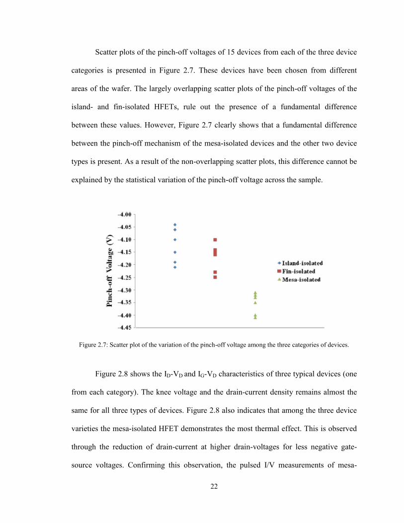
Scatter plots of the pinch-off voltages of 15 devices from each of the three device
categories is presented in Figure 2.7. These devices have been chosen from different
areas of the wafer. The largely overlapping scatter plots of the pinch-off voltages of the
island- and fin-isolated HFETs, rule out the presence of a fundamental difference
between these values. However, Figure 2.7 clearly shows that a fundamental difference
between the pinch-off mechanism of the mesa-isolated devices and the other two device
types is present. As a result of the non-overlapping scatter plots, this difference cannot be
explained by the statistical variation of the pinch-off voltage across the sample.
Figure 2.7: Scatter plot of the variation of the pinch-off voltage among the three categories of devices.
Figure 2.8 shows the ID-VD and IG-VD characteristics of three typical devices (one
from each category). The knee voltage and the drain-current density remains almost the
same for all three types of devices. Figure 2.8 also indicates that among the three device
varieties the mesa-isolated HFET demonstrates the most thermal effect. This is observed
through the reduction of drain-current at higher drain-voltages for less negative gate-
source voltages. Confirming this observation, the pulsed I/V measurements of mesa-
Page 34
23
isolated HFETs show a higher output resistance in the saturation operation regime of
these devices in the aforementioned bias range. This is due to the presence of
proportionally larger surface area for power dissipation in fin- and island-isolated
devices, in comparison to the mesa-isolated HFETs of the same gate-width.
(a) (b)
(c)
Figure 2.8: Scaled drain- and gate-current versus drain-source voltage, for a typical mesa-isolated HFET
(a), fin-isolated HFET (b), and island-isolated HFET (c). On all these figures pulsed drain current values
are indicated in dashed lines. VGS is changed from -5 to 0 V, in steps of 0.5 V.
With further reduction of the size of the isolation mesa and the use of compliant
substrate schemes in heterostructure growth, it is believed that the observed trends can be
further enhanced. The compliant substrate is predicted to act as a decoupling mechanism
between the induced strain on the channel GaN layer by the substrate and the barrier
Page 35
24
layer. This has been theoretically shown to be able to further enhance the relaxation of
strain through lateral definition of mesa [28]. This type of polarization engineering is
expected to be able to considerably shift the pinch-off voltage of AlGaN/GaN HFETs as
the size of isolation mesa reduces to the order of six-times the mesa height [27-32]. To
maintain the same current-drive, these devices can be fabricated through employing a
large number of islands rather than one single mesa. The minimum size of the islands
reported in here has been defined by the constraints of the foundry.
2.5 Conclusion
Two new types of isolation structures for AlGaN/GaN HFETs were introduced: fin- and
island-isolation. A correlation between the size of the isolation feature and the pinch-off
voltage of AlGaN/GaN HFETs was observed. These results indicate a positive shift in the
pinch-off voltage with the reduction of the size of the isolation feature. For the island-
isolated AlGaN/GaN HFETs, the gate transconductance is observed to be relatively
higher. Also, it is observed that island-isolation results in better thermal behavior of the
HFET.
Page 36
25
Chapter 3
Investigation of the Impact of
Temperature Dependency of Drift
Transport Characteristics on the Drain
Current of AlGaN/GaN HEFTs
3.1 Abstract
A Monte Carlo-based temperature dependent mobility model, with incorporation of
steady-state velocity overshoot, is employed in modeling the drain current-voltage
characteristics of AlGaN/GaN HFETs at 300, 400, and 500K. One of the major merits of
this model is that it employs a very small set of fitting parameters. The modeled drain
current-voltage characteristics have been successfully matched to the experimental
characteristics at the aforementioned temperatures. While a brief measurement at these
temperatures is believed to be of no meaningful consequence on the quality of the metal-
semiconductor contacts, this matching confirms that the temperature dependency of the
drift electron velocity is the culprit of degradation of drain current at elevated
temperatures.
Page 37
26
3.2 Introduction
Over the past decade, AlGaN/GaN HFETs have drawn much attention, due to their great
potentials for high power, high frequency, and high temperature applications [2], [15].
The wide bandgap, large peak value of the electron drift-velocity, the very wide steady-
state overshoot in the drift-velocity versus electric-field (i.e. vd-E) characteristics of GaN,
in addition to the unprecedented values of polar sheet-carrier concentrations (i.e. of the
order of 1013
cm-2
) at the pseudomorphically grown AlGaN/GaN heterointerfaces, turn
these devices into great choices for high power microwave signal amplification [33].
The recent major advances in epitaxial growth [34-35], Ohmic contact formation
[17-18], and other device fabrication steps of III-Nitride HFETs have led to an increasing
need for modeling the behavior of these novel devices [12], [36-40]. In such an endeavor,
the particular attributes of transport through these 2DEG channels ought to be fully
included in modeling. Due to the suitability of these devices for high temperature
applications, developing a model for predicting the temperature dependency of the drain
current-voltage (i.e. ID-VD) characteristics is of prime importance.
In the present work, by incorporation of the temperature dependency of the vd-E
characteristics of the 2DEG channel of AlGaN/GaN HFETs, a previously proposed
analytically-manageable drift-diffusion –based model of AlGaN/GaN HFETs (i.e. [40])
has been modified to predict the temperature variation of ID-VD characteristics. The
aforementioned temperature variations of the electron drift transport characteristics of
these channels, in line with the predictions of Bhapkar et al. [41], are provided by a
commercial Monte Carlo-based simulator (i.e. MOCASIM, [42]). The analytical vd-E
Page 38
27
expression, required in the device model, has been constrained for yielding the maximum
similarity to the Monte Carlo–based predictions, at each temperature. Even though the
model has a few fitting parameters, the physical significance of each parameter has been
reserved and studied. In addition, in this revision of the work of Loghmany et al. [40], the
potential drop along the source-access and drain-access regions of the 2DEG channel are
more accurately incorporated. These distinctions are indicated in section 3.4.3.
3.3 Temperature dependency of vd-E characteristics
In obtaining the temperature dependent vd-E characteristics from MOCASIM, only two
of the material parameters of GaN are corrected to match the values referred to in the
work of Bhapkar et al. [41] and O’Leary et al. [16]. These two parameters are the
acoustic deformation potential and polar optical phonon energy, for which values of 8.3
eV and 91.2 meV are introduced to MOCASIM (from [41] and [16]), respectively. All of
the important scattering mechanisms governing the high-temperature drift transport
characteristics through the polar 2DEG channel of the AlGaN/GaN HFETs, including
phonon scattering, polar optical phonon scattering, acoustic phonon scattering, ionized
impurity scattering, intervalley scattering, and piezoelectric scattering are taken into
account by the simulator.
The resulting vd-E characteristics at 300, 400, and 500K are illustrated in Figure
3.1. In order to substantiate the validity of the predictions of this simulator, these
characteristics are compared to a variety of Monte Carlo-based simulations reviewed in
the recently published work of Yang et al. [43]. Over the same temperature range, this
compilation presents identical drift transport characteristics.
Page 39
28
The drain current of AlGaN/GaN HFET is the result of electron transport through
the 2DEG channel. The two-dimensional confinement nature and the degeneracy of
electron population at the heterointerface make the two-dimensional transport of
electrons distinguishable from the three-dimensional electron transport through the bulk
GaN. However, in support of the application of Monte Carlo-based simulations of vd-E
characteristics, obtained for electron transport in bulk GaN, it should be mentioned that
while a meaningful difference is only observed at low electric-fields such an
improvement in low-field electron mobility of 2DEG channel is usually compensated for
by the degrading effect of interface scattering [44-45]. While such a scattering
mechanism impact the electron transport through the 2DEG channels, such an effect is
not considered in the simulator. As a result, the adoption of the vd-E characteristics is
sufficiently accurate.
Figure 3.1: Electron drift transport characteristics of GaN at 300, 400, and 500K from MOCASIM.
0
0.5
1
1.5
2
2.5
3
0 1 2 3 4
T=300K
T=400K
T=500K
Electric Field (V/cm) × 105
Ele
ctro
n D
rift
Vel
oci
ty (
cm/s
ec) ×
10
7
Page 40
29
In order to be able to feed these temperature variable characteristics into the
HFET model of Loghmany et al. [40] parameters of the analytical mobility model used
in that work are tuned for producing the best matched vd-E characteristics to the Monte
Carlo-based drift transport characteristics of Figure 3.1. The aforementioned analytical
mobility model is presented as:
( )
(
)
(
)
(
)
(
)
( )
For best matching to the room-temperature data presented in Figure 3.1, the
values of the parameters of (3.1) are extracted using the least mean-square fitting
technique. The room-temperature values of these parameters are tabulated in Table 3.1.
Table 3.1: Model parameters of (3.1) at 300K.
Parameter Description Value
µ0 Low-field mobility 1113 cm2/(V.s)
µ1 High field mobility 128 cm2/(V.s)
E0 Low electric-field 2.06 × 10⁴ V/cm
E1 High electric-field 12.79 × 10⁴ V/cm
Saturation velocity 1.94 × 107 cm/s
Power index 1.33
Power index 7.10
The temperature-variations of the first five entries of Table (3.1) were found to
follow a power law, as the temperature increases. These variations with reference to
parameter values at room-temperature are given by:
Page 41
30
( ) (
)
( ) ( )
( ) (
)
( ) ( )
( ) (
) ( ) ( )
( ) (
) ( ) ( )
( ) (
) ( ) ( )
The least-mean-square –obtained values of , , , , and are -1.63, -0.06,
0.26, 0.4, and 0.18, respectively. Values of the power indices of (3.1) have been assumed
to be temperature independent. It is physically illustrative that among these values
explicitly agrees with the trend of the temperature-variation of low-field electron mobility
at high temperatures [20], [46]. Figure 3.2 illustrates the matching of these analytical
expressions with the Monte Carlo-based trends (previously shown in Figure 3.1).
Page 42
31
Figure 3.2: Matching of the electron drift transport characteristics shown by the analytical expression (3.1)
with the Mont Carlo-based characteristics of Figure 3.1 at 300, 400, and 500K.
3.4 Drain current modeling of AlGaN/GaN HFETs
According to the model of Loghmany et al. the channel of a non self-aligned
AlGaN/GaN HFET is broken into a combination of three regions: an ungated HFET
representative of the source-access region, a gated HFET located under the gate
electrode, and an ungated HFET representative of the drain-access region [40]. These
regions are identified in Figure 3.3. While due to the special form of the electric-field
variation of HFETs along the channel, in the first part of the channel electric-field values
are small, at high drain-source voltages (at the drain-side of the gated channel and in its
vicinity in the ungated drain-access region) electron drift velocity will go through the
velocity overshoot and eventual saturation [40]. In this model, the part of the channel
with electric-field values below the corresponding value to the peak electron drift
0
0.5
1
1.5
2
2.5
3
3.5
0 1 2 3 4
Monte Carlo
Model
Electric Field (V/cm) × 105
Dri
ft V
elo
city
(cm
/sec)
× 1
07
T=300K to 500K
Page 43
32
velocity is referred to as linear, while the regime of operation in the rest of the channel is
referred to as saturation.
3.4.1 Linear Regime
Assuming the mobility model expressed by (3.1), under the linear regime of
operation Loghmany et al. have presented the variation of channel-potential (i.e. V(x))
according to the following differential equation [40]:
( ( ))( ( )
(
( )
)
(
( )
)
( )
)
((
( )
)
(
( )
)
) ( )
In this equation VT is the threshold voltage, VGT is defined by VG-VT, J is the
current density per unit-width of the transistor, and CCH is the gate capacitance calculated
in terms of dielectric constant of AlGaN (i.e. εAlGaN), AlGaN thickness (i.e. d), and
effective thickness of the 2DEG (i.e. Δd):
( )
Page 44
33
AlGaN
GaN
Source Gate Drain
x=0 x=LG
2DEG
Gated HFET
LGDLGS
d
Δd
Figure 3.3: Basic schematic structure of an AlGaN/GaN HFET. LGS and LGD represent the length of the
ungated HFETs of the source-access and drain-access regions, respectively.
The solution to (3.7) can be obtained by using the backward differentiation
method, with the initial value of the voltage at the source edge of the gate (i.e. V(x=0))
calculated for each value of the current density according to the potential drop across the
series combination of the source-access region resistance and the source contact
resistance.
3.4.2 Saturation Regime
As the electric-field along the channel exceeds the value corresponding to the
maximum electron drift velocity (i.e. Ev-max), reduction of the drift velocity and also
growing significance of the lateral electric-field in calculation of 2DEG carrier density
render the drift-only transport formalism, applied to the linear part of the channel,
inadequate. Loghmany et al. [40], following the footsteps of Grebene et al. [47], have
investigated the potential drop along this region by considering the steady-state drift
Page 45
34
velocity overshoot of the electrons in the AlGaN/GaN HFET channel (Figure 3.1) in
conjunction with the application of the Gauss’ law. The Gaussian box extended
throughout this region is indicated in Figure 3.4. This model indicates the development of
a non-zero gradient in the electron concentration of this part of the channel. As a result,
in applying the current-continuity and continuity of the electric-field along the channel,
for each point along this part of the channel the diffusion current density (i.e. JDiff) should
be calculated and deducted from the total current density to achieve the drift current
component [40].
The resulting expressions for the calculation of the effective threshold voltage
(i.e. VT(x’)) and the component of the electric-field along the length of the channel under
saturation, are given by [40]:
( ) ( )
( )
( ) ( )
( )
( (
)) ( )
where is the drift current density, which is the difference between the total current
density (i.e. J) and the diffusion current density. The effective threshold voltage and its
gradient are in turn used in calculation of the diffusion current. It has been shown that the
assumption of a slightly varying channel-potential along this part of the channel (i.e.
V(x’)) can easily lead these recursive equations to convergence.
Page 46
35
AlGaN
GaN
Gate
d
Y j
Ev-max
x'=0
~Y
j
x
y
z
y
x'
E┴
Ex'(x')
Saturation
Region
x'’E
F
EC
E
Figure 3.4: Schematic illustration of the boundaries of the Gaussian box formed in the saturation region.
The conduction band edge of AlGaN/GaN heterointerface is shown in the inset.
According to this model, for each value of the current density the potential drop
along the length of the channel is calculated by adding up the potential drop along the
channels of the two ungated HFETs of source- and drain-access regions and the channel
of the gated HFET (Figure 3.3). While, the moderate electric-field of the source access-
region deems the consideration of a 2DEG sheet resistance sufficient for studying this
part of the channel, in the drain access-region the ungated HFET should be investigated
as a channel prone to saturation. As a result, the model explained in sections 3.4.1 and
3.4.2, with a few modifications, is applied to this part of the channel. These modifications
include the mathematical consideration of a uniform surface potential, calculated through
establishing the current-continuity and continuity of electric-field at the boundary of the
gated and the ungated HFET [40].
Page 47
36
Considering the absence of a blocking Schottky contact at the surface of the
AlGaN barrier of an ungated HFET, it is evident that the channel will preserve its linear
characteristics up to relatively higher drain-source voltages [48-49]. This fact contributes
to lowering the potential drop along the drain-access region. This is caused by the
mandate of the current-continuity that under the linear regime of operation the electrons
in the more populated 2DEG channel of the ungated HFET should drift more slowly than
in the neighbouring gated HFET. As a result, the electric-field of this part of the channel
is forced to maintain a lower strength (Figure 3.1). Supporting this observation of the
deferred saturation, in this implementation of the model presented in [40], choosing an
appropriate threshold voltage for the channel of the drain-access region under the linear
regime of operation has resulted in a more accurate prediction of the device knee voltage.
This very important improvement in the prediction power of the model is presented in
section 3.5 with regards to the experimental ID-VD characteristics.
3.4.3 Temperature variations of the channel potential
In modeling the temperature variations of the ID-VD characteristics of
AlGaN/GaN HFETs, the temperature-dependent drift transport model presented in
section 3.3 has been applied to the device model of sections 3.4.1 and 3.4.2. In this
implementation, attention has been paid to the thermal characteristics of sheet resistance
in the access regions. This has been observed to be able to improve the predicting power
of the model in comparison to the other temperature-dependent models of AlGaN/GaN
HFETs [50-54]. For the source-access region this variation is quite accurately predicted
in terms of the power-law variation of the low-field electron mobility (i.e. (3.2)) [20].
Page 48
37
For the temperature range of interest of this study (i.e. 300-500K) a change in the
quality of Ohmic and Schottky contacts to the AlGaN/GaN HFET has not been predicted.
As a result these effects are not considered. This assumption is substantiated by the
experimental observations provided in section 3.5. These include the absence of a
temperature-dependent variation of the threshold voltage of the device and also optical
evaluation of the contacts before and after the high-temperature tests (Figure 3.5). It has
also been observed that the high-temperature tests leave no considerable permanent
degradation in the ID-VD characteristics.
Figure 3.5: ID-VG characteristics when VD=1V at T=300 through 500K, in step of 50K.
3.5 Experimental background and discussions
The temperature dependent model, presented in section 3.4, has been assessed versus the
experimentally measured ID-VD characteristics of a number of AlGaN/GaN HFET,
0.0E+00
5.0E-03
1.0E-02
1.5E-02
2.0E-02
2.5E-02
3.0E-02
3.5E-02
4.0E-02
-5 -4 -3 -2 -1 0
Gate-Source Voltage (V)
Dra
in C
urr
ent
(A)
T=300 to 500K
in step of 50K
Page 49
38
measured at temperatures of 300, 400, and 500K. The device characteristics used in these
evaluations have been typical characteristics of the device behaviors observed across the
wafer.
The HFET epitaxial layers of the devices explored in this study have been grown
on a SiC substrate. Details of the layer structure are shown in Figure 2.2. To review these
details it should be mentioned that this structure is composed of a 20 nm -thick AlGaN
barrier of thirty percent Al-composition, a 1 nm -thick AlN spacer layer sandwiched
between the AlGaN barrier and GaN channel, and a GaN channel layer. The thickness of
the unintentionally-doped GaN channel layer is 200 nm. Device fabrication was carried
out by CMC. Device design has been performed according to the process flow of this
foundry, which has been explained in Chapter 2.
Absence of frequency dispersion in the drain current and gate-transconductance of
the measured devices and high values of gate-transconductance (i.e. of the order of 250
mS/mm), and drain current density (i.e. of the order of 1 A/mm) of these devices are
indicative of good quality of surface passivation and processing [55]. A strong saturating
characteristic of the drain current is also observed. As a result, conclusions drawn from
the modeling of the ID-VD characteristics of these devices fairly assess the high-
temperature transport problem of AlGaN/GaN HFETs.
The device layout is shown in Figure 3.6, whereas the vertical and horizontal
device dimensions are tabulated in Table 3.2. Also in this table, the parameters adopted in
the application of the model, presented in section 3.4, to these devices are summarized.
Page 50
39
Source
Source
Source
Source
Gate
Drain
Gate
electrode
Source
Ohmic
contact
Via1 Mesa
boundry
Contact
openings
Drain
Ohmic
contact
Figure 3.6: Device layout of a two-finger AlGaN/GaN HFET with micro-strip interconnects.
Table 3.2: Device parameters and parameters used in the model.
Symbol Description Value
LG Gate Length 1 μm
LGD Drain-access region length 2 μm
LGS Source-access region length 1.1 μm
W Channel width 100 μm
RCS and RCD Source and drain contact resistivity 0.73 Ohm.mm
(provided by the
foundry)
Rsh Channel sheet resistance 262 Ohm/sq
d Barrier thickness 21 nm
Δd 2DEG thickness 2 nm
VT Threshold voltage -4.1 V
Page 51
40
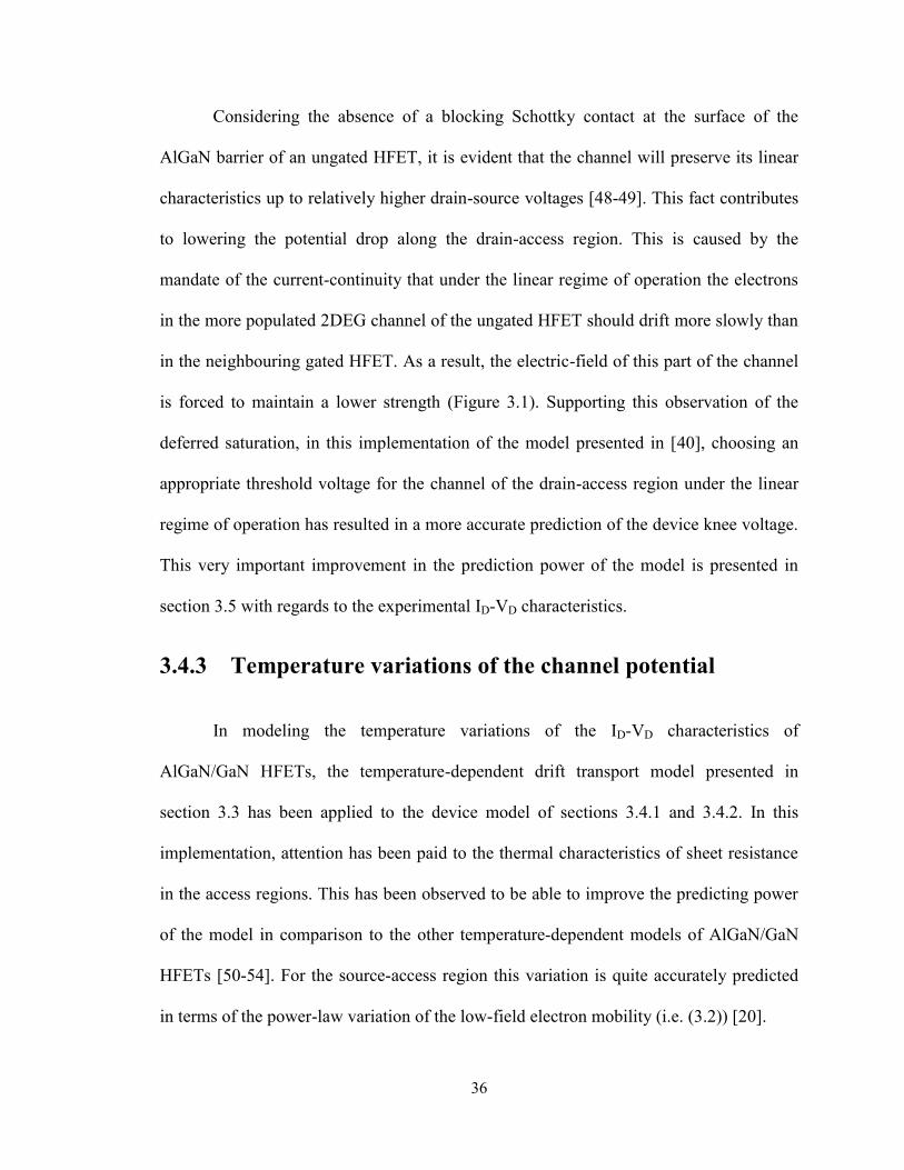
3.5.1 Assessment of the temperature-dependent device model
In all the measurements reported in here, a Keithley semiconductor parameter
analyzer was used. Measurements were done in the pulsed-mode with short pulses of
small duty-cycle to avoid self-heating. Figure 3.7 illustrates the agreement between the
experimentally-measured and modeled room-temperature ID-VD characteristics of the
AlGaN/GaN HFET reported earlier in this section. The superb match between these two
characteristics is indicative of the importance of the correct assessment of the deferred
saturation of the ungated drain-access region (indicated in section 3.4.2). The model
explained in section 3.4 has been implemented numerically with the use of the finite
difference technique. Modeling has been performed for the gate voltages not too close to
the threshold voltage. The reason for that is that the model presented in section 3.4
assumes zero leakage through the substrate and as a result it is not capable of correctly
reproducing the ID-VD characteristics close to the threshold voltage [40].
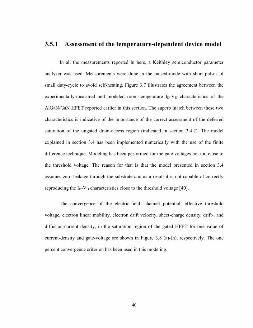
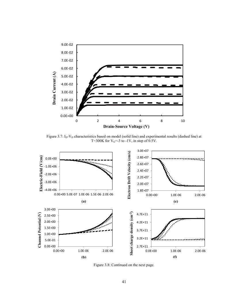
The convergence of the electric-field, channel potential, effective threshold
voltage, electron linear mobility, electron drift velocity, sheet-charge density, drift-, and
diffusion-current density, in the saturation region of the gated HFET for one value of
current-density and gate-voltage are shown in Figure 3.8 (a)-(h), respectively. The one
percent convergence criterion has been used in this modeling.
Page 52
41
Figure 3.7: ID-VD characteristics based on model (solid line) and experimental results (dashed line) at
T=300K for VG=-3 to -1V, in step of 0.5V.
Figure 3.8: Continued on the next page.
0.0E+00
1.0E-02
2.0E-02
3.0E-02
4.0E-02
5.0E-02
6.0E-02
7.0E-02
8.0E-02
9.0E-02
0 2 4 6 8 10
Drain-Source Voltage (V)
Dra
in C
urr
ent
(A)
-4.0E+06
-3.0E+06
-2.0E+06
-1.0E+06
0.0E+00
0.0E+00 5.0E-07 1.0E-06 1.5E-06 2.0E-06
Ele
ctri
c-F
ield
(V
/cm
)
(a)
1.8E+07
2.0E+07
2.2E+07
2.4E+07
2.6E+07
2.8E+07
3.0E+07
0.0E+00 1.0E-06 2.0E-06
Ele
ctr
on
Drif
t V
elo
cit
y (
cm
/s)
(e)
0.0E+00
5.0E-01
1.0E+00
1.5E+00
2.0E+00
2.5E+00
3.0E+00
0.0E+00 1.0E-06 2.0E-06
Ch
an
nel
Po
ten
tia
l (V
)
(b)
2.7E+11
3.2E+11
3.7E+11
4.2E+11
4.7E+11
0.0E+00 1.0E-06 2.0E-06
Sh
eet
cha
rge d
ensi
ty (
cm-2
)
(f)
Page 53
42
Figure 3.8: Convergence of electric-field (a), channel-potential distribution (b), effective threshold-voltage
(c), linear electron mobility (d), electron drift velocity (e), sheet charge density distribution (f), diffusion
current density (g), and drift current density (h) at VG=-3 V and current density equal to 1.378 A/cm at
T=300K, where final results are shown in solid line, initial guesses for electric-field, channel potential, and
effective threshold-voltage is shown in dashed lines, and iterations are shown in dotted lines.
Figures 3.9(a) and (b) illustrate the superb match between the modeled and the
experimentally measured ID-VD characteristics at 400 and 500K, respectively. The on-
chip high temperature measurements have been performed using the enclosed chamber of
an MMR probe station. Samples were kept at the measurement temperature long-enough
to reach the steady-state condition. In obtaining the modeled characteristics, the
temperature variation of the transport in all three regions of gated-channel, source-, and
drain-access are considered, as outlined in section 3.4.
-7.0E+00
-6.0E+00
-5.0E+00
-4.0E+00
-3.0E+00
-2.0E+00
-1.0E+00
0.0E+00
0.0E+00 1.0E-06 2.0E-06
Eff
ecti
ve
Th
resh
old
-Vo
ltg
e (
V)
(c)
-1.4E-01
-1.2E-01
-1.0E-01
-8.0E-02
-6.0E-02
-4.0E-02
-2.0E-02
0.0E+00
2.0E-02
0.0E+00 1.0E-06 2.0E-06
Dif
fusi
on
Cu
rren
t D
ensi
ty (
A/c
m)
(g)
0.0E+00
2.0E+01
4.0E+01
6.0E+01
8.0E+01
1.0E+02
1.2E+02
1.4E+02
1.6E+02
1.8E+02
0.0E+00 1.0E-06 2.0E-06
Ele
ctro
n D
rift
mo
bil
ity
(cm
2/V
.s)
(d)
Position along region II (cm)
1.36
1.38
1.40
1.42
1.44
1.46
1.48
1.50
1.52
0.0E+00 1.0E-06 2.0E-06Dri
ft C
urr
en
t D
ensi
ty (
A/c
m)
(h)
Position along region II (cm)
Page 54
43
In order to demonstrate the importance of considering the temperature-
dependency of transport in the access regions, Figure 3.10 depicts the modeled drain
characteristics versus the experimental data with only considering the temperature-
dependency of transport in the gated-channel. The degradation in prediction of the knee-
voltage and the saturation characteristics are clearly indicative of the importance of
studying the temperature variation of the sheet resistance in the access region.
Figure 3.9: ID-VD characteristics based on model (solid line) and experimental results (dashed line) at
T=400 (a), and 500K (b), for VG=-3 to -1V in step of 0.5V. The temperature variation of the sheet
resistance in the access region is fully considered.
0.0E+00
1.0E-02
2.0E-02
3.0E-02
4.0E-02
5.0E-02
6.0E-02
0 2 4 6 8 10
Drain-Source Voltage (V)
(a)
Dra
in C
urr
ent
(A)
0.0E+00
1.0E-02
2.0E-02
3.0E-02
4.0E-02
5.0E-02
6.0E-02
0 2 4 6 8 10Drain-Source Voltage (V)
(b)
Dra
in C
urr
ent
(A)
Page 55
44
Figure 3.10: ID-VD characteristics based on model (solid line) and experimental results (dashed line) at
T=400 (a), and 500K (b), for VG=-3 to -1V in step of 0.5V. The temperature variation of the sheet
resistance in the access region is not considered.
3.5.2 Role of the accurate modeling of high-field drift-
velocity in high-temperature device modeling
Many of the existing device models, while paying attention to the low-field
electron mobility of the AlGaN/GaN channel, approximate the high-field electron drift
0.0E+00
1.0E-02
2.0E-02
3.0E-02
4.0E-02
5.0E-02
6.0E-02
0 2 4 6 8 10Drain-Source Voltage (V)
Dra
in C
urr
ent
(A)
0.0E+00
1.0E-02
2.0E-02
3.0E-02
4.0E-02
5.0E-02
0 2 4 6 8 10Drain-Source Voltage (V)
Dra
in C
urr
ent
(A)
Page 56
45
velocity in terms of a purely-saturating vd-E characteristic [36]. In order to assess the
degree of accuracy of this assumption at higher temperatures, in this part two different
mobility models with different degrees of accuracy in following the temperature-
dependent vd-E characteristics resulted from MOCASIM simulations are investigated:
Transport model (1): In this model the low-field electron mobility (i.e. µ0) is
assumed to be temperature independent, while the temperature dependency of the other
parameters of (3.1) are assessed for yield maximum similarity to the Monte Carlo-based
transport characteristics at high electric-fields.
Transport model (2): In this model, only the temperature variation of the low-field
mobility (i.e. µ0) is considered in order to yield maximum similarity to the Monte Carlo-
based transport characteristics at low to moderate electric-fields, while other parameters
of (3.1) are assumed temperature independent.
Figures 3.11(a) and (b) depict the predictions of the first and the second model in
comparison to the MOCASIM-calculated characteristics, which were also shown in
Figure 3.1, respectively.
The adoption of the transport models (1) and (2), to the device model of section
3.4, result in the ID-VD characteristics shown in Figures 3.12 and 3.13, respectively. As
shown in these figures, for temperatures of 400 and 500K, the inaccuracy inherent to the
transport model (1) leaves a much more pronounced impact on the predicting power of
the analytical device model. The inherent inaccuracy of the transport model (2) in
following the high electric-field transport is observed to merely result in the slightly
erroneous calculation of the knee voltage.
Page 57
46
These observations confirm that maintaining the accuracy in modelling of low-
field electron mobility and steady-state overshoot of drift velocity are much more
important in producing an accurate model, than the accuracy in correctly following the
saturation velocity. In order to study the degree of this approximation as the temperature
is raised, the difference in the value of current density at the onset of deviation of drift
velocity from μ0E (referred to in here as onset of saturation) with the value of saturated
current density is studied. These values at temperatures of 300, 400, and 500K for a few
gate-voltages are tabulated in Tables 3.3, 3.4, and 3.5, respectively. As shown in these
tables, with the elevation in temperature especially at gate voltages farther away from
threshold, the current density at the onset of saturation region becomes proportionally
less important in calculation of the current-drive in saturation. As a result, for these
conditions purely maintaining the accuracy of the value of the low-filed electron
mobility, which is the dominant factor under the linear regime of operation, would be less
acceptable.
Page 58
47
(a)
(b)
Figure 3.11: Matching of the electron drift transport characteristics shown by the analytical expression (3.1)
with the Mont Carlo-based characteristics of Figure 3.1 at 300, 400, and 500K, according to the transport
model (1) and (2), respectively shown in (a) and (b).
0
0.5
1
1.5
2
2.5
3
3.5
0 1 2 3 4
Monte Carlo
Model
Electrical Field (V/cm) × 105
Dri
ft V
eloci
ty (
cm/s
ec) ×
10
7
T=300K to 500K
T=500K
0
0.5
1
1.5
2
2.5
3
3.5
0 1 2 3 4
Monte Carlo
Model
Electrical Field (V/cm) × 105
Dri
ft V
eloci
ty (
cm/s
ec) ×
10
7
T=300K to 500K
Page 59
48
Figure 3.12: ID-VD characteristics based on the transport model (1) (solid line) and experimental results
(dashed line) at T=400 (a), and 500K (b), for VG=-3 to -1V in step of 0.5V.
0.0E+00
1.0E-02
2.0E-02
3.0E-02
4.0E-02
5.0E-02
6.0E-02
7.0E-02
8.0E-02
0 2 4 6 8 10
Drain-Source Voltage (V)
(a)
Dra
in C
urr
en
t (A
)
0.0E+00
1.0E-02
2.0E-02
3.0E-02
4.0E-02
5.0E-02
6.0E-02
7.0E-02
8.0E-02
0 2 4 6 8 10
Drain-Source Voltage (V)
(b)
Dra
in C
urr
ent
(A)
Page 60
49
Figure 3.13: ID-VD characteristics based on the transport model (2) (solid line) and experimental results
(dashed line) at T=400 (a), and 500K (b), for VG=-3 to -1V in step of 0.5V.
0.0E+00
1.0E-02
2.0E-02
3.0E-02
4.0E-02
5.0E-02
0 2 4 6 8 10
Drain-Source Voltage (V)
(a)
Dra
in C
urr
ent
(A)
0.0E+00
1.0E-02
2.0E-02
3.0E-02
4.0E-02
5.0E-02
0 2 4 6 8 10
Drain-Source Voltage (V)
(b)
Dra
in C
urr
ent
(A)
Page 61
50
Table 3.3: Current density at the onset of saturation and saturation current density at 300K.
VG (V) Current density at
the onset of
saturation (A/cm)
Saturation
current density
(A/cm)
Percentage of the
saturation current
density at the
onset saturation
-3 1.317 1.361 96.7
-2.5 2.323 2.441 95.1
-2 3.435 3.663 93.7
-1.5 4.615 4.987 92.5
-1 5.840 6.389 91.4
Table 3.4: Current density at the onset of saturation and saturation current density at 400K.
VG
(V)
Current density at
the onset of
saturation (A/cm)
Saturation
current density
(A/cm)
Percentage of the
saturation current
density at the onset
saturation
-3 0.9 0.939 95.8
-
2.5
1.615 1.725 93.6
-2 2.412 2.634 91.5
-
1.5
3.264 3.634 89.8
-1 4.150 4.71 88.1
Table 3.5: Current density at the onset of saturation and saturation current density at 500K.
VG (V) Current density at
the onset of
saturation (A/cm)
Saturation
current
density (A/cm)
Percentage of the
saturation
current density
at the onset
saturation
-3 0.664 0.698 95.1
-2.5 1.206 1.305 92.4
-2 1.815 2.020 89.8
-1.5 2.467 2.820 87.5
-1 3.149 3.688 85.3
Page 62
51
3.6 Conclusions
A capable analytical framework with manageable degree of computational difficulty is
proposed for modeling the high-temperature drain current-voltage characteristics of
AlGaN/GaN HFETs. The model takes into account the temperature-dependence of
transport through the gated-channel of an AlGaN/GaN HFET and also its access regions.
This model is validated with regards to the experimentally measured drain current
characteristics. In light of this work, it is shown that maintaining a high degree of
accuracy in the incorporated transport model into the analytical models developed for
modeling the drain-current behavior of AlGaN/GaN HFETs becomes more important
with the increase of device operation temperature. In this work, self-heating and non
steady-state transport and thermal effects have not been considered. This is a condition
suitable for relatively -long-channel devices operating under the low duty-cycle pulsed
operation mode.
Page 63
52
Chapter 4
Conclusion and Future Work
One goal of this thesis was to pursue on a different approach (through strain-relief) to
open a new avenue for fabrication and design of enhancement-mode AlGaN/GaN
HFETs, side by side the high current-density depletion-mode AlGaN/GaN HFETs. This
is beneficial to applications such as direct connected transistor logic (DCTL).
Experimental results, although unsuccessful in achieving enhancement-mode operation,
are encouraging in terms of positive shifting of the threshold voltage. This achievement
is the first indication of the possibility of exerting control over the threshold voltage of
AlGaN/GaN HFETs through the definition of mesa geometry.
In chapter 2, the impact of the size of the isolation-mesa on the sweeping- and pulsed-
mode drain current-voltage characteristics of AlGaN/GaN HFETs has been studied.
Investigations reveal that while by implementing AlGaN/GaN HFETs on array of islands
or mesas of smaller dimensions, rather than one continuous-mesa, same values for the
maximum drain current level can be maintained, pinch-off voltage can be made less
negative. Also, the maximum gate transconductance will be improved by island-type
isolation. It is also observed that the proportionally larger surface area for power
dissipation in fin- and island-isolated HFETs can reduce the impact of heating on
AlGaN/GaN HFETs.
Page 64
53
Due to the fabrication constraints of the foundry, the minimum size of the isolated
mesas reported in this work was limited. Further driving-down the size of the isolation-
mesas of AlGaN/GaN HFETs is extremely important in further studying the correlation
between the positive shift in pinch-off voltage and the mesa geometry.
Modeling the drain current of AlGaN/GaN HFETs at high temperature ambient was
the other objective of this thesis, since high temperature ambient is a probable
environment for these high-power devices, such a model is extremely beneficial in
providing guidelines for device design in this technology.
In chapter 3, an adequate analytical framework is proposed for modeling the high-
temperature drain current-voltage characteristics of AlGaN/GaN HFETs. The model
takes into account the temperature-dependence of transport through the gated-channel of
an AlGaN/GaN HFET and also its access regions. This model is validated with regards to
the experimentally measured drain current characteristics. In light of this work, it is
shown that maintaining a high degree of accuracy in the incorporated transport model
(into the analytical models developed for modeling the drain-current behavior of
AlGaN/GaN HFETs) becomes more important with the increase of device operation
temperature.
As future works in these two areas the following are suggested:
- Experimental strain analysis and characterization of the small isolated mesas of
AlGaN/GaN epilayer.
- Experimentation of strain-relief on epilayers grown on compliant diaphragms.
- Theoretical study of the proposed strain-relief strategy.
Page 65
54
- Incorporation of self-heating, gate- and substrate leakage, and non steady-state
transport in the presented analytical model.
Page 66
55
Bibliography
[1] M. Khan, Q. Chen, J. Yang, M. Anwar, M. Blasinggame, M. Shur, J. Burm, and
L. Eastman, ―Recent advances in III-V nitride electron devices,‖ IEDM Tech.
Dig., pp. 27-30, Dec. 1996.
[2] S. Wood, R. Pengelly, D. Farrell, C. Platis, and J. Crescenzi ―High-power, high-
efficiency GaN HEMT power amplifiers for 4G applications,‖ High Freq. Elec.,
pp. 36-47, May 2009.
[3] Y. Arakawa, ―Progress in GaN-based quantum dots for optoelectronics
applications,‖ IEEE journal of selected topics in quantum electronics, vol. 8, no.
4, pp. 823-833, July/Aug. 2002.
[4] O. Ambacher, J. Smart, J. Shealy, N. Weimann, K. Chu, M. Murphy, W. Schaff,
L. Eastman, R. Dimitrov, L. Wittmer, M. Stutzmann, W. Rieger, and J.
Hilsenbeck, ―Two-dimensional electron gases induced by spontaneous and
piezoelectric polarization charges in N- and Ga-face AlGaN/GaN
heterostructures,‖ J. Appl. Phys., vol. 85, no. 6, pp. 3222-3233, Mar. 1999.
[5] U. Mishra and J. Singh, Semiconductor Device Physics and Design, Springer,
2008.
[6] K. Takahashi, A. Yoshikawa, and A. Sandhu, Wide bandgap semiconductors:
fundamental properties and modern photonic and electronic devices, Springer,
2007.
[7] S. Adachi, Properties of Group-IV, III-V and II-VI Semiconductors, John Wiley
and Sons, 2005.
[8] F. Bernardini, V. Fiorentini, and D. Vanderbilt, ―Spontaneous polarization and
piezoelectric constants of III–V nitrides,‖ Phys. Rev. B, vol. 56, no. 16, pp. R10-
024–R10-027, Oct. 1997.
[9] M. Khan, A. Bhattarai, J. Kuznia, and D. Olson, ―High electron mobility
transistor based on a GaN AlxGa1-xN heterojunction,‖ Appl. Phys. Lett., vol. 63,
no. 9, pp. 1214-1215, Aug. 1993.
[10] M. Khan, J. Kuznia, D. Olson, W. Schaff, J. Burm, and M. Shur, ―Microwave
performance of a 0.25μm gate AlGaN/GaN heterostructure field effect transistor,‖
Appl. Phys. Lett., vol. 65, no. 9, pp. 1121-1123, Aug. 1994.
[11] E. Yu and E. Manasreh, ―Spontaneous and piezoelectric polarization in nitride
heterostructures,‖ in III-V Nitride Semiconductors: Applications and Devices
Page 67
56
(Optoelectronic Properties of Semiconductors and Superlattices), pp. 161-193,
Taylor & Francis, 2003.
[12] J. Albrecht, R. Wang, P. Ruden, M. Farahmand, K. Brennan, ―Electron transport
characteristics of GaN for high temperature device modeling,‖ J. Appl. Phys D.,
vol. 83, no. 9, pp. 4777-4781, May 1998.
[13] D. Florescu, V. Asnin, F. Pollak, A. Jones, J. Ramer, M. Schurman, and I.
Ferguson, ―Thermal conductivity of fully and partially coalesced lateral epitaxial
overgrown GaN/sapphire (0001) by scanning thermal microscopy,‖ Appl. Phys.
Lett., vol. 77, no. 10, pp. 1464-1466, Sep. 2000.
[14] Y. Guhel, B. Boudart, V. Hoel, M. Werquin, C. Gaquiere, J. De Jaeger, M.
Poisson, I. Daumiller, and E. Kohn, ―Effects of high temperature on the electrical
behavior of AlGaN/GaN HEMTs,‖ Microwave and Optic. Tech. Lett., vol. 34, no.
1, July 2002.
[15] R. Menozzi, G. Umana-Membreno, B. Nener, G. Parish, G. Sozzi, L. Faraone,
and U. K. Mishra, ―Temperature-dependent characterization of AlGaN/GaN
HEMTs: thermal and source/drain resistances,‖ IEEE Trans Dev. Mat. Reli., vol.
8, no. 2, pp. 255-264, June 2008.
[16] S. O’Leary, B. Foutz, M. S. Shur, and L. Eastman, ―Steady-state and transient
electron transport within the III-V nitride semiconductors, GaN, AlN, and InN: A
review,‖ J. Mater. Sci: Mater. Electronics, vol. 17, no. 2, pp. 87–126, Feb. 2006.
[17] F. Mohammed, L. Wang, H. Koo, and I. Adesida, ―Anatomy-performance
correlation in Ti-based contact metallizations on AlGaN/GaN heterostructures,‖ J.
Appl. Phys., vol. 101, no. 3, pp. 033708-1-15, Feb. 2007.
[18] L. Wang, F. Mohammed, and I. Adesida, ―Difference in the reaction kinetics
formation mechanisms of annealed Ti/Al/Mo/Au Ohmic contacts on n-GaN and
AlGaN/GaN epilayers,‖ J. Appl. Phys., vol. 101, no. 1, pp. 013702-11, Jan. 2007.
[19] M. Khan, X. Hu, A. Tarakji, G. Simin, G. Simin, J. Yang, R. Gaska, and M. Shur,
―AlGaN/GaN metal–oxide–semiconductor heterostructure field-effect transistors
on SiC substrates,‖ Appl. Phys. Lett., vol. 77, no. 9, pp. 1339 - 1341, Aug. 2000.
[20] Z. Liu, S. Arulkumaran, and G. Ng, ―Temperature dependence of Ohmic contact
characteristics in AlGaN/GaN high electron mobility transistors from −50 to
200°C,‖ Appl. Phys. Lett., vol. 94, no. 14, pp. 142105-3, Apr. 2009.
[21] V. Fiorentini, F. Bernardini, and O. Ambacher, ―Evidence for nonlinear
macroscopic polarization in III-V nitride alloy heterostructures,‖ Appl. Phys. Lett.,
vol. 80, pp. 1204-1206, Feb. 2002
Page 68
57
[22] W. Lanford, T. Tanaka, Y. Otoki, and I. Adesida, ―Recessed-gate enhancement-
mode GaN HEMT with high threshold voltage,‖ Elec. Lett., vol. 41, pp. 449-450,
Mar. 2005.
[23] T. Palacios, C. Suh, A. Chakraborty, S. Keller, S. DenBaars, and U. Mishra,
―High-Performance E-Mode AlGaN/GaN HEMTs,‖ IEEE Elec. Dev. Lett., vol.
27, no. 6, pp. 428-430, June 2006.
[24] Y. Cai, Y. Zhou, K. Lau, and K. Chen, ―High performance enhancement-mode
AlGaN/GaN HEMTs using fluoride-based plasma treatment,‖ IEEE Elec. Dev.
Lett., vol. 26, pp. 435-437, 2005.
[25] Y. Uemoto, M. Hikita, H. Ueno, H. Matsuo, H. Ishida, M. Yanagihara, T. Ueda,
T. Tanaka, and D. Ueda, ―Gate Injection Transistor (GIT)—A Normally-Off
AlGaN/GaN Power Transistor Using Conductivity Modulation,‖ IEEE Trans.
Elec. Dev., vol. 54, no. 12, pp. 3393–3399, Dec. 2007.
[26] S. Senturia, Microsystem Design, Springer, 2000.
[27] F. Huang, ―Theory of strain relaxation for epitaxial layers grown on substrate of a
finite dimension,‖ Phys. Rev. Lett., vol. 85, pp. 784-787, July 2000.
[28] A. Fischer, H. Kühne, B. Roos, and H. Richter, ―Elastic strain relaxation in
patterned heteroepitaxial structures,‖ Semicond. Sci. Tech., vol. 9, pp. 2195-2198,
1994.
[29] G. Kästner and U. Gösele, ―Reduced critical thickness for relaxing heteroepitaxial
films on compliant substrates,‖ Appl. Phys. Lett., vol. 82, pp. 3209-3211, May
2003.
[30] S. Jain, K. Pinardi, H. Maes, R. van Overstraeten, and M. Willander ―Effects of
elastic constants on the stresses in stripes and substrates: a 2D FE calculation,‖
Semicond. Sci. Tech., vol. 13, pp. 864-870, 1998.
[31] P. Nikolov, Y. Bolkhovityanov, O. Pchelyakov, S. Romanov, and L. Sokolov
―Specific behavior of stress relaxation in GexSi1-x films grown on porous silicon
based mesa substrates: computer calculations,‖ Semicond. Sci. Tech., vol. 18, pp.
39-44, 2003.
[32] K. Usuda, T. Irisawa, T. Numata, N. Hirashita, and S. Takagi ―Characterization of
in-plane strain relaxation in strained layers using a newly developed plane nano-
beam electron diffraction (plane-NBD) method,‖ Semicond. Sci. Tech., vol. 22,
pp. 227-230, 2007.
[33] O. Ambacher, B. Foutz, J. Smart, J. Shealy, N. Weimann, K. Chu, M. Murphy, A.
Sierakowski, W. Schaff, L. Eastman, R. Dimitrov, A. Mitchell, and M.
Stutzmann, ―Two dimensional electron gases induced by spontaneous and
Page 69
58
piezoelectric polarization in undoped and doped AlGaN/GaN heterostructures,‖ J.
Appl. Phys., vol. 87, no. 1, pp. 234-244, Jan. 2000.
[34] T. Palacios, A. Chakraborty, S. Heikman, S. Keller, S. P. DenBaars, and U. K.
Mishra, ―AlGaN/GaN High electron mobility transistors with InGaN back-
barriers,‖ IEEE Elec. Dev. Lett., vol. 27, no. 1, pp.13-15, Jan. 2006.
[35] A. Denis, G. Goglio, and G. Demazeau,‖ Gallium nitride bulk crystal growth
processes: A review,‖ Mat. Sci. and Eng. R, vol. 50, no. 6, pp. 167-194, Jan. 2006.
[36] A. Koudymov, M. S. Shur, G. Simin, K. Chu, P. Chao, C. Lee, J. Jimenez, and A.
Balistreri, ―Analytical HFET I-V model in presence of current collapse,‖ IEEE
Trans. Elec. Dev., vol. 55, no. 3, pp. 712-720, Mar. 2008.
[37] M. Moradi and P. Valizadeh, ―Analytical Modeling of Current Collapse in
AlGaN/GaN HFETs According to the Virtual Gate Concept,‖ IEEE Trans. on
Dev. and Mat. Reli., vol. 10, no. 2, pp. 287-294, June 2010.
[38] M. Moradi and P. Valizadeh, ―Influence of transferred-electron effect on drain-
current characteristics of AlGaN/GaN heterostructure field-effect transistors,‖ J.
Appl. Phys., vol. 109, no. 2, pp. 024509-8, Jan. 2011.
[39] X. Cheng and Y. Wang, ―A Surface-Potential-Based Compact Model for
AlGaN/GaN MODFETs,‖ IEEE Trans. Elec. Dev., vol. 58, no. 2, pp. 448-454,
Feb. 2011.
[40] A. Loghmany and P. Valizadeh, ―Analytical modeling of drain-current
characteristics of AlGaN/GaN HFETs with full incorporation of steady-state
velocity overshoot,‖ J. Appl. Phys D., vol. 44, no. 12, pp. 125102-8, Mar. 2011.
[41] U. Bhapkara and M. Shur, ―Monte Carlo calculation of velocity-field
characteristics of wurtzite GaN,‖ J. Appl. Phys., vol. 82, no. 4, pp. 1649-1655,
Aug. 1997.
[42] http://www.silvaco.com/ (SILVACO Inc.)
[43] L. Yang, Y. Hao, Q. Yao, and J. Zhang, ―Improved Negative Differential
Mobility Model of GaN and AlGaN for a Terahertz Gunn Diode,‖ IEEE Trans.
Elec. Dev., vol. 58, no. 4, pp. 1076-1083, Apr. 2011.
[44] M. Ramonas, A. Matulionis, and L. Rota, ―Monte Carlo simulation of hot-phonon
and degeneracy effects in the AlGaN/GaN two-dimensional electron gas
channel,‖ Semicond. Sci. Tech., vol. 18, no. 2, pp. 118-132, Jan. 2003.
[45] T. Yu and K. Brennan, ―Monte Carlo calculation of two-dimensional electron
dynamics in GaN–AlGaN heterostructures,‖ J. Appl. Phys., vol. 91, no. 6, pp.
3730-3735, Mar. 2002.
Page 70
59
[46] http://www.ioffe.rssi.ru/SVA/NSM/Semicond/GaN/electric.html
[47] A. Grebene and S. Ghandhi, ―General theory for pinched operation of the
junction-gate FET,‖ Solid-State Electronics, vol. 12, no. 7, pp. 573-589, July
1969.
[48] J. Albrechtt, P. Ruden, S. Binari, К. Ikossi-Anastasiou, M. Ancona, R. Henry, D.
Koleske, and A. Wickenden, ―Current-voltage characteristics of ungated
AlGaN/GaN heterostructures,‖ Proc. Mat. Res. Soc. Symp., vol. 572, 1999.
[49] L. Ardaravičius, A. Matulionis, J. Liberis, O. Kiprijanovic, M. Ramonas, L.
Eastman, J. Shealy, and A. Vertiatchikh, ―Electron drift velocity in AlGaN/GaN
channel at high electric fields,‖ Appl. Phys. Lett., vol. 83, no. 19, pp. 4038-4040,
Nov. 2003.
[50] Y. Chang, K. Y. Tong, and C. Surya, ―Numerical simulation of current–voltage
characteristics of AlGaN/GaN HEMTs at high temperatures,‖ Semicond. Sci.
Tech., vol. 20, no. 2, pp. 188-192, Jan. 2005.
[51] Y. Chang, Y. Zhang, Y. Zhang, and K. Tong, ―A thermal model for static current
characteristics of AlGaN/GaN high electron mobility transistors including self-
heating effect,‖ J. Appl. Phys D., vol. 99, no. 4, pp. 044501-5, Feb. 2006.
[52] M. Huque, S. Eliza, T. Rahman, H. Huq, and S. Islam, ―Temperature dependent
analytical model for current–voltage characteristics of AlGaN/GaN power
HEMT,‖ Sol. Stat. Elec., vol. 53, no. 3, pp.341-348, Mar. 2009.
[53] X. Cheng, M. Li, and Y. Wang, ―An analytical model for current–voltage
characteristics of AlGaN/GaN HEMTs in presence of self-heating effect,‖ Sol.
Stat. Elec., vol. 54, no. 13, pp.42-46, Jan. 2010.
[54] S. Vitanov, V. Palankovski, S. Maroldt, and R. Quay, ―High-temperature
modeling of AlGaN/GaN HEMTs,‖ Sol. Stat. Elec., vol. 54, no. 10, pp. 1105-
1112, Oct. 2010.
[55] M. Higashiwaki, N. Onojima, T. Matsui, and T. Mimura, ―Effects of SiN
passivation by catalytic chemical vapour deposition on electrical properties of
AlGaN/GaN heterostructure field-effect transistors,‖ J. Appl. Phys., vol. 100, no.
3, pp. 0337141-0337146, Aug. 2006.