73
© 2011 TSMC, Ltd TSMC Property DAC 2014 Tutorial 8 Sang Dhong and Jean-Pierre Colinge TSMC June 2, 2014 FinFET to NanoWire Transistor: Extending Moore’s Law to Sub 10 nm TUTORIAL 8

© 2011 TSMC, Ltd
TSMC Property
DAC 2014 Tutorial 8
Sang Dhong and Jean-Pierre Colinge TSMC
June 2, 2014
FinFET to NanoWire Transistor: Extending Moore’s Law to Sub 10 nm
TUTORIAL 8

© 2011 TSMC, Ltd
TSMC Property
1
DAC 2014 Tutorial 8
ABSTRACT
FinFETs and tri-gate FETs have extended Moore's law down to a gate length of 20-15nm. A Silicon Nanowire Transistor (NWT) is one of the most promising devices which could give further gate length scaling to 10-5 nm, potentially to 3 nm. At these dimensions, quantum confinement and effects should be understood for proper development of functional CMOS circuits and robust design methodology. The tutorial will cover briefly the transition needed from a conventional planar transistor to a FinFET in device physics, circuit and methodology, followed by a detailed description of enhancing channel control by a gate through higher-dimensional multi-gate structures, Gate-All-Around Nanowire FETs. It can have vertical or horizontal transistor architectures, each with its own advantages and possible drawbacks. Discussion of circuit prospects of NWT in the fields of CMOS logic, volatile and non-volatile memory, and integrated sensors will be concluded by expected changes in circuits and methodology for transition from FinFET to NWT, including quantum effects.

© 2011 TSMC, Ltd
TSMC Property
2
DAC 2014 Tutorial 8
Outline
A bit of history….. How did we get here?
Short-channel effects and multigate FETs
Nanowire transistor architectures
FinFET to NWT: Logic and SRAM applications
Modeling FinFET to NWT
Programmable devices and sensors in NWT
New Physics…Quantum Effects … New materials…
Conclusion
© 2011 TSMC, Ltd
TSMC Property
3
DAC 2014 Tutorial 8
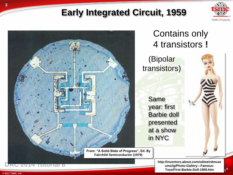
Early Integrated Circuit, 1959
Contains only
4 transistors !
(Bipolar
transistors)
From: “A Solid-State of Progress”, Ed. By
Fairchild Semiconductor (1979)
Same
year: first
Barbie doll
presented
at a show
in NYC
http://inventors.about.com/od/weirdmuse
ums/ig/Photo-Gallery---Famous-
Toys/First-Barbie-Doll-1959.htm

© 2011 TSMC, Ltd
TSMC Property
4
DAC 2014 Tutorial 8
Early Integrated Circuit, 1969
(200 MOS transistors)
From: “A Solid-State of Progress”, Ed. By
Fairchild Semiconductor (1979)
Same year:
First man
on the
Moon
Woodstock
festival
http://tribune.com.pk/story/426282/first-man-on-
moon-neil-armstrong-dead-at-82-us-media/
http://www.inthestudio.net/online-on-demand/woodstock-pt-2/

© 2011 TSMC, Ltd
TSMC Property
5
DAC 2014 Tutorial 8
NVIDIA’s Kepler GK110, 2013
(7,080,000,000 transistors)
http://www.nvidia.com/content/PDF/kepler/NVIDIA-Kepler-GK110-Architecture-Whitepaper.pdf
Same year:
Higgs Boson
Nobel Prize
http://physicsworld.com/cws/article/news/2012/jul/04/cern-discovers-higgs-like-boson
5

© 2011 TSMC, Ltd
TSMC Property
6
DAC 2014 Tutorial 8
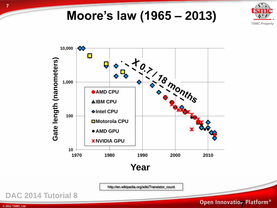
Moore’s law (1965 – 2013)
6
© 2011 TSMC, Ltd
TSMC Property
7
DAC 2014 Tutorial 8
Moore’s law (1965 – 2013)
http://en.wikipedia.org/wiki/Transistor_count
7
10
100
1,000
10,000
1970 1980 1990 2000 2010
Gate
len
gth
(n
an
om
ete
rs)
AMD CPU
IBM CPU
Intel CPU
Motorola CPU
AMD GPU
NVIDIA GPU
Year

© 2011 TSMC, Ltd
TSMC Property
DAC 2014 Tutorial 8
© 2011 TSMC, Ltd
TSMC Property
9
DAC 2014 Tutorial 8
Outline
A bit of history….. How did we get here?
Short-channel effects and multigate FETs
Nanowire transistor architectures
FinFET to NWT: Logic and SRAM applications
Modeling FinFET to NWT
Programmable devices and sensors in NWT
New Physics…Quantum Effects … New materials…
Conclusion
© 2011 TSMC, Ltd
TSMC Property
10
DAC 2014 Tutorial 8
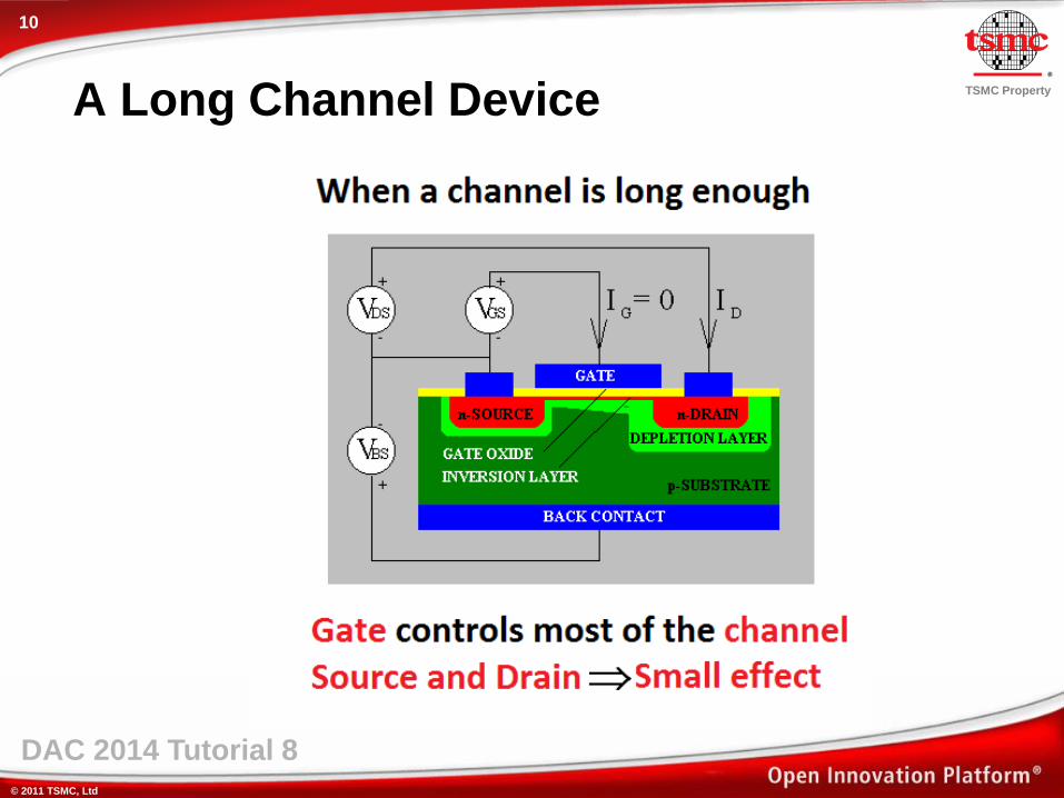
A Long Channel Device
© 2011 TSMC, Ltd
TSMC Property
11
DAC 2014 Tutorial 8
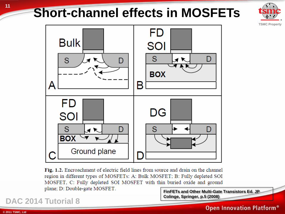
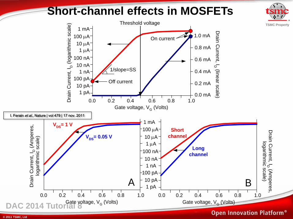
Short-channel effects in MOSFETs
FinFETs and Other Multi-Gate Transistors Ed. JP
Colinge, Springer, p.5 (2008)
© 2011 TSMC, Ltd
TSMC Property
DAC 2014 Tutorial 8
1 pA
10 pA
100 pA
1 nA
10 nA
100 nA
1 A
10 A
100 A
1 mA
0.0 0.2 0.4 0.6 0.8 1.0
Dra
in C
urr
en
t, I
D (
Am
pe
res,
log
arith
mic
sca
le)
Gate voltage, VG (Volts)
0.0 0.2 0.4 0.6 0.8 1.0
Gate voltage, VG (Volts)
VDS
= 0.05 V
VDS
= 1 V
Long
channel
Short
channel
Dra
in C
urre
nt, ID
(Am
pe
res,
log
arith
mic
sca
le)
A B
1 pA
10 pA
100 pA
1 nA
10 nA
100 nA
1 A
10 A
100 A
1 mA
1.0 mA
0.8 mA
0.6 mA
0.4 mA
0.2 mA
0.0 mA0.0 0.2 0.4 0.6 0.8 1.0
1/slope=SSD
rain
Cu
rre
nt, I
D (
log
arith
mic
sca
le)
Dra
in C
urre
nt, ID
(line
ar s
ca
le)
Off current
On current
Threshold voltage
Gate voltage, VG (Volts)
I. Ferain et al., Nature | vol 479 | 17 nov. 2011
Short-channel effects in MOSFETs
© 2011 TSMC, Ltd
TSMC Property
13
DAC 2014 Tutorial 8
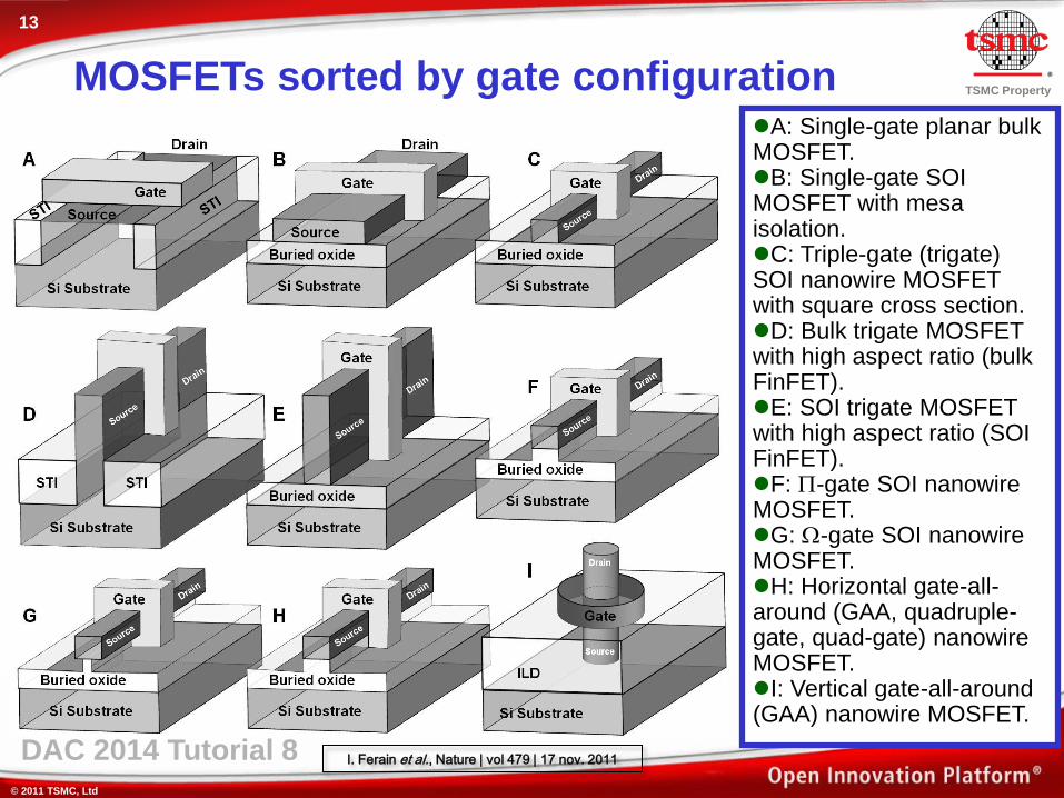
A: Single-gate planar bulk MOSFET. B: Single-gate SOI MOSFET with mesa isolation. C: Triple-gate (trigate) SOI nanowire MOSFET with square cross section. D: Bulk trigate MOSFET with high aspect ratio (bulk FinFET). E: SOI trigate MOSFET with high aspect ratio (SOI FinFET). F: P-gate SOI nanowire MOSFET. G: W-gate SOI nanowire MOSFET. H: Horizontal gate-all-around (GAA, quadruple-gate, quad-gate) nanowire MOSFET. I: Vertical gate-all-around (GAA) nanowire MOSFET.
MOSFETs sorted by gate configuration
I. Ferain et al., Nature | vol 479 | 17 nov. 2011
© 2011 TSMC, Ltd
TSMC Property
14
DAC 2014 Tutorial 8
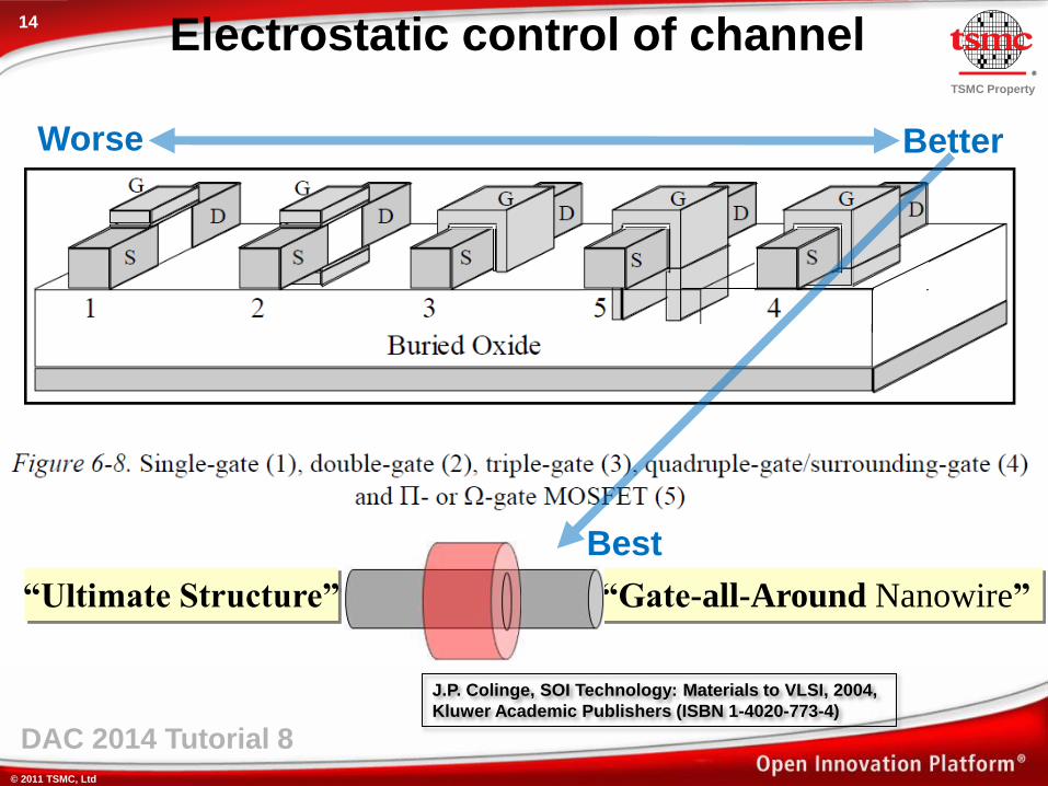
Electrostatic control of channel
“Gate-all-Around Nanowire”
J.P. Colinge, SOI Technology: Materials to VLSI, 2004,
Kluwer Academic Publishers (ISBN 1-4020-773-4)
Worse Better
“Ultimate Structure”
Best

© 2011 TSMC, Ltd
TSMC Property
15
DAC 2014 Tutorial 8
Electrostatic control of channel:
Poisson’s equation
2
2
2
2
2
2 ),,(),,(),,(
dz
zyxd
dy
zyxd
dx
zyxd
I. Ferain et al., Nature | vol 479 | 17 nov. 2011
© 2011 TSMC, Ltd
TSMC Property
16
DAC 2014 Tutorial 8
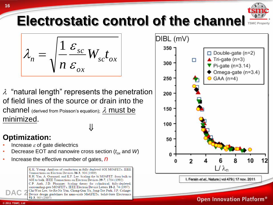
l “natural length” represents the penetration
of field lines of the source or drain into the
channel (derived from Poisson’s equation); l must be
minimized.
Optimization: • Increase of gate dielectrics
• Decrease EOT and nanowire cross section (tox and W)
• Increase the effective number of gates, n
oxsc
ox
scn tW
n
l
1
(“n”=effective number of gates,
W is the nanowire cross section)
I. Ferain et al., Nature | vol 479 | 17 nov. 2011
Electrostatic control of the channel
© 2011 TSMC, Ltd
TSMC Property
17
DAC 2014 Tutorial 8
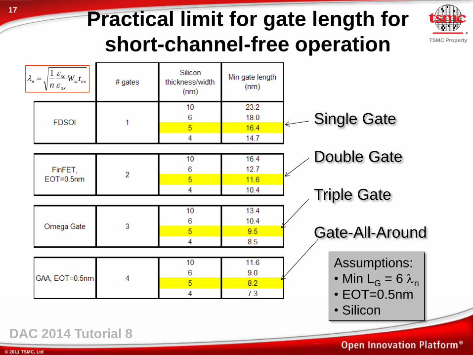
Assumptions:
• Min LG = 6 ln
• EOT=0.5nm
• Silicon
Practical limit for gate length for
short-channel-free operation
oxsc
ox
scn tW
n
l
1
Single Gate
Double Gate
Triple Gate
Gate-All-Around
© 2011 TSMC, Ltd
TSMC Property
18
DAC 2014 Tutorial 8
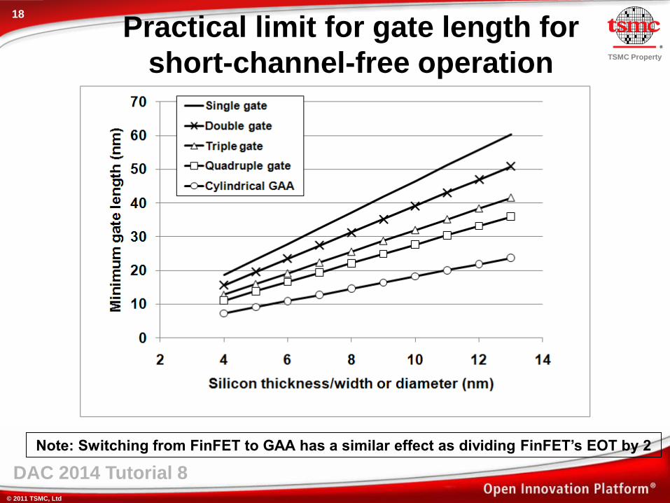
Note: Switching from FinFET to GAA has a similar effect as dividing FinFET’s EOT by 2
Practical limit for gate length for
short-channel-free operation
© 2011 TSMC, Ltd
TSMC Property
19
DAC 2014 Tutorial 8
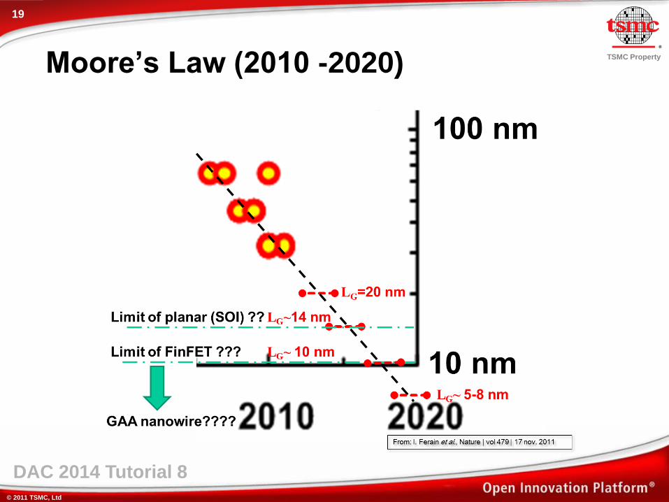
Moore’s Law (2010 -2020)

© 2011 TSMC, Ltd
TSMC Property
20
DAC 2014 Tutorial 8
Outline
A bit of history….. How did we get here?
Short-channel effects and multigate FETs
Nanowire transistor architectures
FinFET to NWT: Logic and SRAM applications
Modeling FinFET to NWT
Programmable devices and sensors in NWT
New Physics…Quantum Effects … New materials…
Conclusion

© 2011 TSMC, Ltd
TSMC Property
21
DAC 2014 Tutorial 8
How small can you go?
© 2011 TSMC, Ltd
TSMC Property
DAC 2014 Tutorial 8
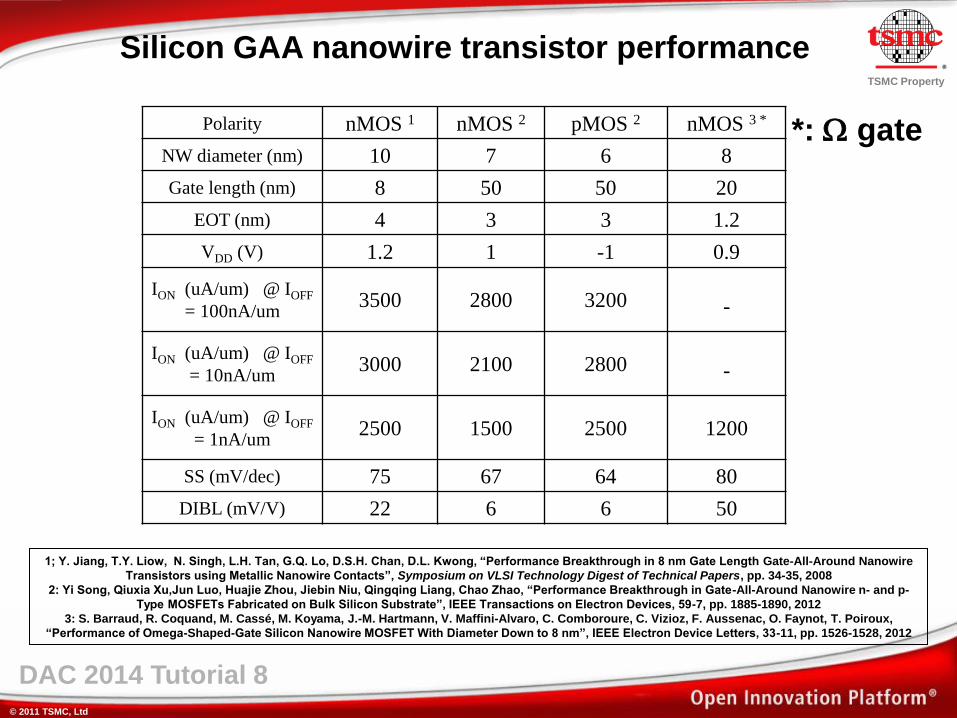
Polarity nMOS 1 nMOS 2 pMOS 2 nMOS 3 *
NW diameter (nm) 10 7 6 8
Gate length (nm) 8 50 50 20
EOT (nm) 4 3 3 1.2
VDD (V) 1.2 1 -1 0.9
ION (uA/um) @ IOFF
= 100nA/um 3500 2800 3200
-
ION (uA/um) @ IOFF
= 10nA/um 3000 2100 2800
-
ION (uA/um) @ IOFF
= 1nA/um 2500 1500 2500 1200
SS (mV/dec) 75 67 64 80
DIBL (mV/V) 22 6 6 50
1; Y. Jiang, T.Y. Liow, N. Singh, L.H. Tan, G.Q. Lo, D.S.H. Chan, D.L. Kwong, “Performance Breakthrough in 8 nm Gate Length Gate-All-Around Nanowire
Transistors using Metallic Nanowire Contacts”, Symposium on VLSI Technology Digest of Technical Papers, pp. 34-35, 2008
2: Yi Song, Qiuxia Xu,Jun Luo, Huajie Zhou, Jiebin Niu, Qingqing Liang, Chao Zhao, “Performance Breakthrough in Gate-All-Around Nanowire n- and p-
Type MOSFETs Fabricated on Bulk Silicon Substrate”, IEEE Transactions on Electron Devices, 59-7, pp. 1885-1890, 2012
3: S. Barraud, R. Coquand, M. Cassé, M. Koyama, J.-M. Hartmann, V. Maffini-Alvaro, C. Comboroure, C. Vizioz, F. Aussenac, O. Faynot, T. Poiroux,
“Performance of Omega-Shaped-Gate Silicon Nanowire MOSFET With Diameter Down to 8 nm”, IEEE Electron Device Letters, 33-11, pp. 1526-1528, 2012
Silicon GAA nanowire transistor performance
*: W gate

© 2011 TSMC, Ltd
TSMC Property
DAC 2014 Tutorial 8
IEDM 2011
Stacked gates in vertical nanowires
for compact NAND operation
Source
Drain
Gat
e
Source
Drain

© 2011 TSMC, Ltd
TSMC Property
24
DAC 2014 Tutorial 8
Vertical GAA transistors
G. Larrieu and X.-L. Han, “Vertical nanowire array-based
field effect transistors for ultimate scaling”, Nanoscale,
Vol. 5, p. 2437 (2013)

© 2011 TSMC, Ltd
TSMC Property
25
DAC 2014 Tutorial 8
Do you need PN junctions to make a FET?
Junctionless Transistor ↔ Water Hose
Gate Control ↔ Squeeze
For a thicker
Water pipe,
No Difference
in water flow
Water flows
Water stops For a garden hose

© 2011 TSMC, Ltd
TSMC Property
26
DAC 2014 Tutorial 8
Short-channel effects can be further
improved using junctionless NW FETs
Short-channel characteristics improved by Electrostatic
Squeezing effect (depletion in S&D) LG_OFF > LG_physical
LG_physical
LG_OFF
© 2011 TSMC, Ltd
TSMC Property
27
DAC 2014 Tutorial 8
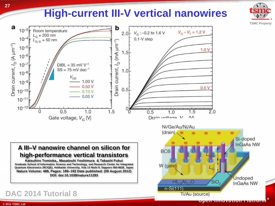
A III–V nanowire channel on silicon for
high-performance vertical transistors Katsuhiro Tomioka,, Masatoshi Yoshimura & Takashi Fukui
Graduate School of Information Science and Technology, and Research Center for Integrated
Quantum Electronics (RCIQE), Hokkaido University, Kita 13 Nishi 8, Sapporo 060-8628, Japan
Nature Volume: 488, Pages: 189–192 Date published: (09 August 2012)
DOI: doi:10.1038/nature11293
High-current III-V vertical nanowires

© 2011 TSMC, Ltd
TSMC Property
DAC 2014 Tutorial 8
G. Ramanathan, Z. X. Chen, N. Singh, K. Banerjee, S. J. Lee, “CMOS Compatible
Vertical Silicon Nanowire Gate-All-Around p-type Tunneling FETs with ≤ 50 mV/decade
Subthreshold Swing”, IEEE Electron Device Letters, 32-11, pp. 1504-1506, 2011)
Silicon GAA Nanowire Tunnel FETs
Tunnel FETs also benefit from
electrostatic control improvements
brought about by GAA architecture
and nanowire diameter reduction

© 2011 TSMC, Ltd
TSMC Property
29
DAC 2014 Tutorial 8
Heterojunction nanowires
A.W. Dey, J. Svensson, M. Ek, E. Lind, C. Thelander, L.E. Wernersson, “Combining Axial and Radial Nanowire Heterostructures: Radial Esaki Diodes and Tunnel Field-Effect Transistors”, Nano Letters, Vol. 13, no. 12, pp. 5919−5924 (2013)
A: Axial heterojunction.
B: Multiple axial heterojunctions.
C: Radial heterojunction (core-shell nanowire).
D: Combination of radial and axial heterojunctions
© 2011 TSMC, Ltd
TSMC Property
30
DAC 2014 Tutorial 8
Outline
A bit of history….. How did we get here?
Short-channel effects and multigate FETs
Nanowire transistor architectures
FinFET to NWT: Logic and SRAM applications
Modeling FinFET to NWT
Programmable devices and sensors in NWT
New Physics…Quantum Effects … New materials…
Conclusion

© 2011 TSMC, Ltd
TSMC Property
31
DAC 2014 Tutorial 8
FinFET Cross-Section
© 2011 TSMC, Ltd
TSMC Property
32
DAC 2014 Tutorial 8
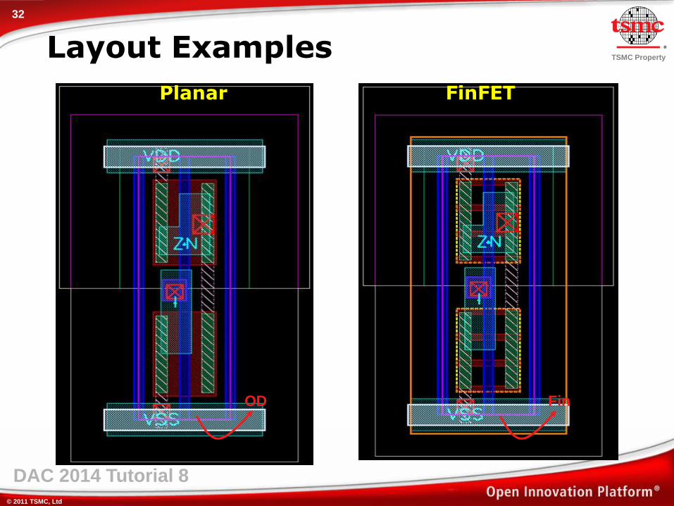
Layout Examples
Planar FinFET
OD Fin

© 2011 TSMC, Ltd
TSMC Property
33
DAC 2014 Tutorial 8
Challenges in Scaling CMOS SRAM
The most challenge is SCE (Short Channel Effect) control
Requires heavy channel doping (>1018 cm-3) and heavy super-halo implants to control surface leakage
Side effects of the heavy doping
Carrier mobility is severely degraded due to impurities scattering
High transverse electric field in the device “ON” state
The increased depletion charge density results in a larger depletion capacitance hence a larger sub-threshold slope.
Off-state leakage current increase due to band-to-band tunneling between the body and drain.
Vt variation caused by Random Dopant Fluctuation (RDF) is another concern for planar CMOS
© 2011 TSMC, Ltd
TSMC Property
34
DAC 2014 Tutorial 8
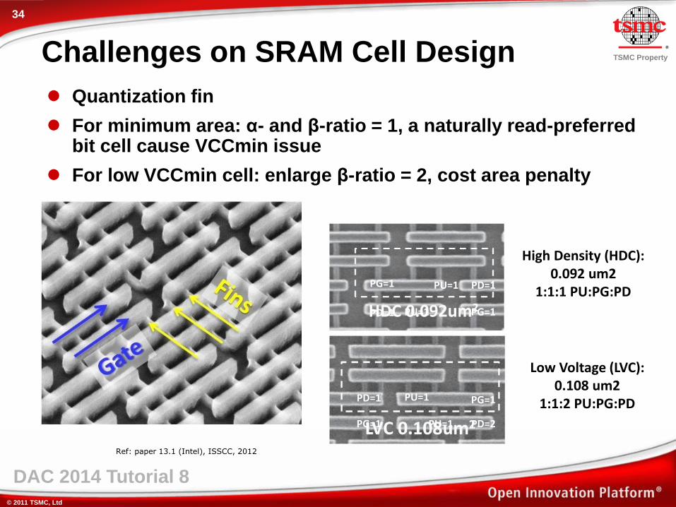
Challenges on SRAM Cell Design
Quantization fin
For minimum area: α- and β-ratio = 1, a naturally read-preferred bit cell cause VCCmin issue
For low VCCmin cell: enlarge β-ratio = 2, cost area penalty
High Density (HDC): 0.092 um2
1:1:1 PU:PG:PD
Low Voltage (LVC): 0.108 um2
1:1:2 PU:PG:PD
Ref: paper 13.1 (Intel), ISSCC, 2012
PU=1
PU=1 PD=1
PD=1
PG=1
PG=1
PU=1
PU=1 PG=1
PG=1
PD=1
PD=2
© 2011 TSMC, Ltd
TSMC Property
35
DAC 2014 Tutorial 8
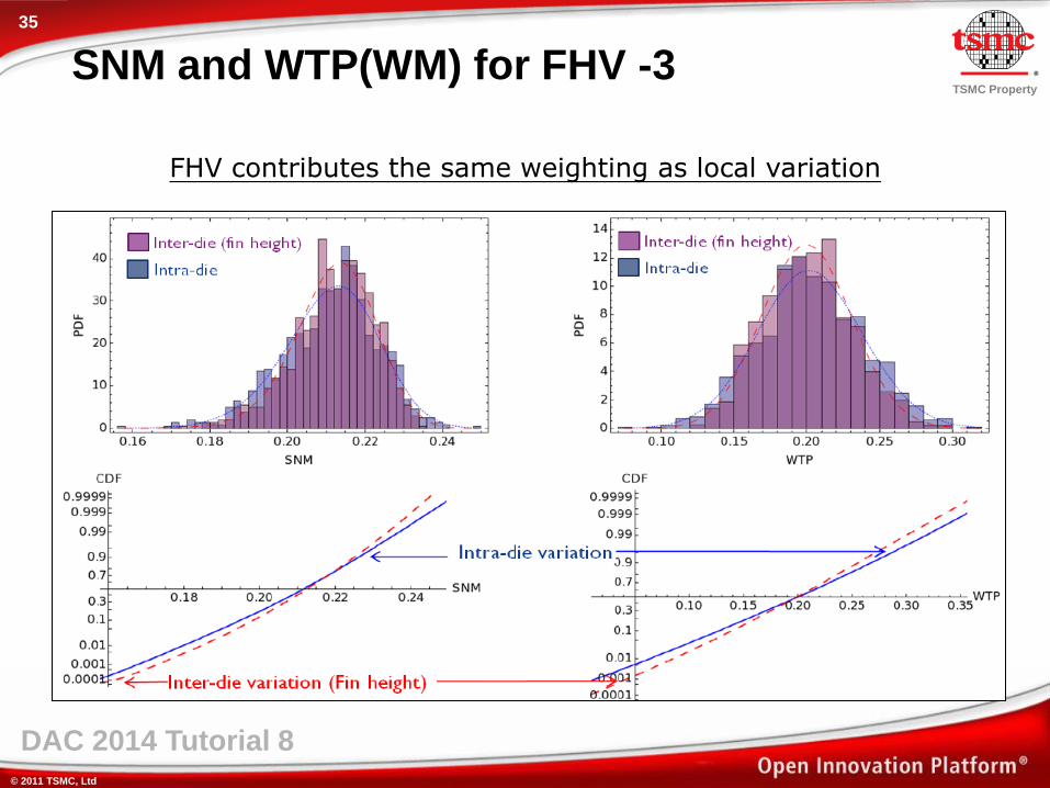
SNM and WTP(WM) for FHV -3
FHV contributes the same weighting as local variation
© 2011 TSMC, Ltd
TSMC Property
DAC 2014 Tutorial 8
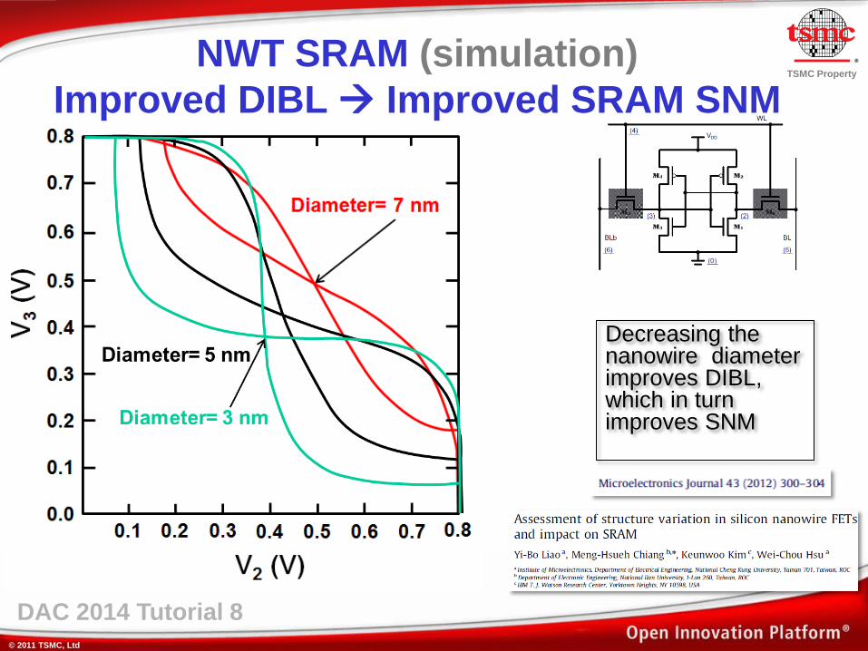
Decreasing the nanowire diameter improves DIBL, which in turn improves SNM
NWT SRAM (simulation)
Improved DIBL Improved SRAM SNM

© 2011 TSMC, Ltd
TSMC Property
DAC 2014 Tutorial 8
Improved DIBL Improved SRAM SNM
(simulation)
Yiming Li, Chien-Sung Lu, “Characteristic Comparison of SRAM Cells with 20 nm Planar MOSFET,
Omega FinFET and Nanowire FinFET”, Proceedings of the 6th IEEE Conference on
Nanotechnology (IEEE-NANO), pp. 339-342 (2006)
Increasing the effective number of gates (Single gate Omega – GAA) improves DIBL, which in turn improves SNM
SN
M (
mV
)

© 2011 TSMC, Ltd
TSMC Property
DAC 2014 Tutorial 8
S. D. Suk, Y. Y. Yeoh, M. Li, K. H. Yeo, S.-H. Kim, D.-W. Kim,
D. Park, W.-S. Lee, “TSNWFET for SRAM cell application:
Performance Variation and Process Dependency”, Proceedings
Symposium on VLSI Technology, pp. 38–39 (2008)
Measured read SNM versus supply voltage VDD for 6T SRAM cells made of either planar MOSFETs or GAA nanowire FETs. Gate length is 40 nm. The nanowire RAM cells achieve a read SNM of 325 mV at a supply voltage of 1 V, while the corresponding cell made with planar transistors achieves an SNM of only 160 mV
NWT SRAM (Experimental)
Improved DIBL Improved SRAM SNM
© 2011 TSMC, Ltd
TSMC Property
39
DAC 2014 Tutorial 8
Outline
A bit of history….. How did we get here?
Short-channel effects and multigate FETs
Nanowire transistor architectures
FinFET to NWT: Logic and SRAM applications
Modeling FinFET to NWT
Programmable devices and sensors in NWT
New Physics…Quantum Effects … New materials…
Conclusion
© 2011 TSMC, Ltd
TSMC Property
40
DAC 2014 Tutorial 8
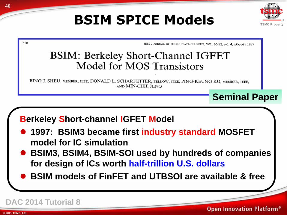
Berkeley Short-channel IGFET Model
1997: BSIM3 became first industry standard MOSFET
model for IC simulation
BSIM3, BSIM4, BSIM-SOI used by hundreds of companies
for design of ICs worth half-trillion U.S. dollars
BSIM models of FinFET and UTBSOI are available & free
BSIM SPICE Models
Seminal Paper
© 2011 TSMC, Ltd
TSMC Property
41
DAC 2014 Tutorial 8
BSIM-CMG for FinFET
Core Model
Surface Potential Equation
Drain Current
Capacitance Model
Real Device Effects
Symmetry / Continuity Tests
Model Availability
A versatile model for double-gate, triple-gate, even cylindrical gate FET.
Passed Industry FinFET Standard balloting in Jan. 2012. Available now.
BSIM-IMG
A related model for Ultra-Thin-Body SOI
Available now (used by ST Microelectronics).
This slide is provided by UC Berkeley Prof. Chenming Hu

© 2011 TSMC, Ltd
TSMC Property
42
DAC 2014 Tutorial 8
Common-Multi-Gate Modeling
Common Multi-gate (BSIM-CMG):
All gates tied together
Surface-potential-based core I-V and C-V model
Supports double-gate, triple-gate, quadruple-gate, cylindrical-gate; Bulk and SOI substrates
This slide is provided by UC Berkeley Prof. Chenming Hu

© 2011 TSMC, Ltd
TSMC Property
43
DAC 2014 Tutorial 8
NANA
Surface Potential Core (FinFET)
Surface potential is obtained from solution
of Poisson’s equation & Gauss’ Law.
Poisson’s equation inside the body can be
written as (Vch is channel potential)
Body doping complicates the solution of the Poisson’s equation.
Perturbation approach is used to solve this problem.
Ref. M. Dunga et al., IEEE TED, No. 9, 2006; M. Dunga, et al., VLSI 2007; Mohan Dunga, PhD Dissertation, UC Berkeley. Slide provided by Prof. C. Hu
Net Surface Potential Inversion Carriers only Perturbation due to finite doping
inv pertψ ψ ψ
© 2011 TSMC, Ltd
TSMC Property
44
DAC 2014 Tutorial 8
Fin/PO/OD Local Density Impact (FinFET)
With HKMG, device uniformity shows higher variation in traditional layout style
MG (metal gate) Hi-Resistor array with center effect
Affected by STI dishing due to low OD density
MOS array with edge effect
Edge devices of MOS array with higher variation due to poly gradient between array and surrounding patterns
Interference among analog blocks due to each with different and wide spreading density on poly and OD
Fin density is likely new factor to impact device uniformity
New layout style and flow needed to minimize this effect
Gradient control on density from array to surrounding patterns

© 2011 TSMC, Ltd
TSMC Property
45
DAC 2014 Tutorial 8
FinFET Design Flow Impact -1
Quantized Fin Limit the flexibility of IP porting
Due to discrete width
Fin on track limits the flexibility on analog block floor plan
Need CAD tool to optimize the quantized width and off-grid issue
Minimum 2-Fin transistor will limit the flexibility of low power design
Single-Fin transistor is desirable to have.
* If Fin Width=Fw (nm), Fin space Fs (nm), Fin Must be in
OD edge.
OD Width=Fw+ (Fw+Fs)*n
© 2011 TSMC, Ltd
TSMC Property
46
DAC 2014 Tutorial 8
FinFET Design Flow Impact -2
Fin/PO/OD density control flow to minimize the device variation
Calculate sensitive analog
block’s density
Surround the sensitive blocks
with a ring of dummy patterns
conventional
Dummy pattern
Insertion related
Prioritize blocks by its
sensitive level and mark cad
layer (ANARRAY_H/M)
Place the non-sensitive
analog blocks
Place Fin/OD/PO patterns
within small density
difference in the
surrounding region
Fill the outside with
conventional dummy utility
and keep IP DRC clean
Place together the sensitive
blocks which have similar
densities

© 2011 TSMC, Ltd
TSMC Property
47
DAC 2014 Tutorial 8
Nanowire transistor modeling (I) As long as the diameter is large enough (approx. 6-8nm for Si), classical drift-
diffusion simulations can be used
In smaller devices, quantum confinement effects must be considered, including the formation of energy sub-bands and inter-band/intra-band scattering mechanisms. This necessitates to solve both Poisson and Schrodinger’s equations self-consistently.
0 1 2 3 4 5
x 1020
-0.56
-0.5598
-0.5596
-0.5594
-0.5592
-0.559
-0.5588
-0.5586
-0.5584
-0.5582
-0.558
Density of States * Fermi distribution (cm-3
eV-1
)
En
erg
y a
bo
ve E
c (
eV
)E
ne
rgy a
bo
ve E
co (e
V)
Density of states (cm-3 eV-1)
150 eV
Color-coded electron density in the different subbands of an n-channel nanowire transistor vs. position along the channel (x-axix) and energy above conduction band (y-axis)

© 2011 TSMC, Ltd
TSMC Property
48
DAC 2014 Tutorial 8
Nanowire transistor modeling (II)
As gate length is reduced, more and more ballistic transport is used (less phonon scattering). This has the potential to boost current drive.
© 2011 TSMC, Ltd
TSMC Property
49
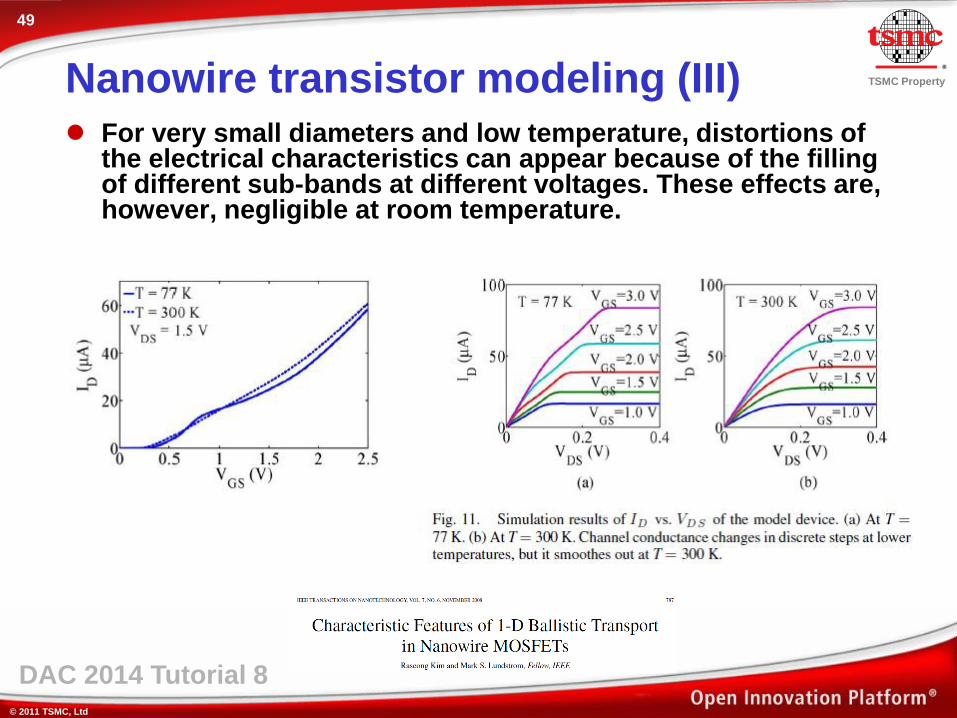
DAC 2014 Tutorial 8
Nanowire transistor modeling (III) For very small diameters and low temperature, distortions of
the electrical characteristics can appear because of the filling of different sub-bands at different voltages. These effects are, however, negligible at room temperature.
© 2011 TSMC, Ltd
TSMC Property
50
DAC 2014 Tutorial 8
Outline
A bit of history….. How did we get here?
Short-channel effects and multigate FETs
Nanowire transistor architectures
FinFET to NWT: Logic and SRAM applications
Modeling FinFET to NWT
Programmable devices and sensors in NWT
New Physics…Quantum Effects … New materials…
Conclusion

© 2011 TSMC, Ltd
TSMC Property
51
DAC 2014 Tutorial 8
Source
Drain
NAND stacked gates
Stacked GAA Vertical NW NAND Flash Memory
© 2011 TSMC, Ltd
TSMC Property
52
DAC 2014 Tutorial 8
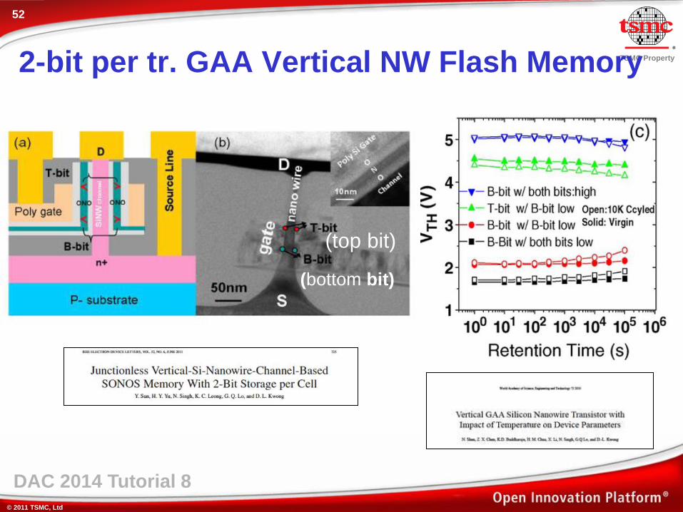
(top bit)
(bottom bit)
2-bit per tr. GAA Vertical NW Flash Memory

© 2011 TSMC, Ltd
TSMC Property
53
DAC 2014 Tutorial 8
VLSI-TSA 2011
GAA Vertical Nanowire Flash Memory Concept
© 2011 TSMC, Ltd
TSMC Property
DAC 2014 Tutorial 8
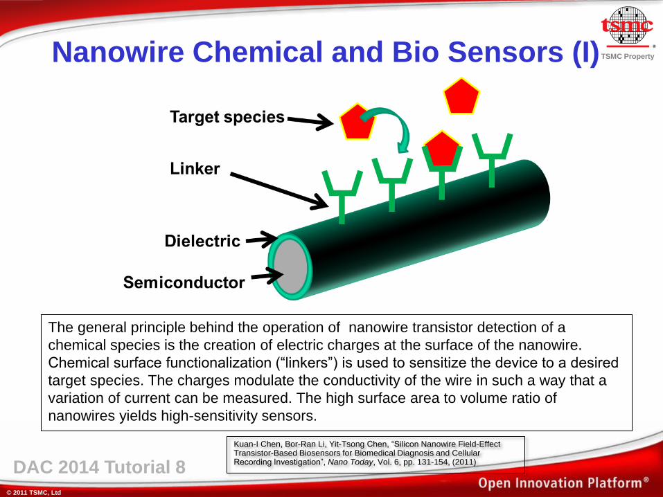
Kuan-I Chen, Bor-Ran Li, Yit-Tsong Chen, “Silicon Nanowire Field-Effect Transistor-Based Biosensors for Biomedical Diagnosis and Cellular Recording Investigation”, Nano Today, Vol. 6, pp. 131-154, (2011)
The general principle behind the operation of nanowire transistor detection of a
chemical species is the creation of electric charges at the surface of the nanowire.
Chemical surface functionalization (“linkers”) is used to sensitize the device to a desired
target species. The charges modulate the conductivity of the wire in such a way that a
variation of current can be measured. The high surface area to volume ratio of
nanowires yields high-sensitivity sensors.
Nanowire Chemical and Bio Sensors (I)

© 2011 TSMC, Ltd
TSMC Property
DAC 2014 Tutorial 8
Ran Yu et al., “Si Junctionless Transistor for Sensing Application: Subthreshold Region Sensor”, Proceedings EUROSOI Conference (2013)
Drain current in a back-gated Si
nanowire pH detector with a diameter
of 20nm and a length of 1 um.
Since the detection takes place in the channel region, the nanowire cannot be fully surrounded by a gate stack, in order to expose a portion of the sensitive channel region to the ambient. This is usually done using one of the following methods:
Back gating technique: One can use a back gate (such as the silicon substrate underneath the buried oxide in the case of an SOI nanowire) to modulate the current in the device while most of the channel surface area is exposed to the ambient. Liquid gating technique: Gating can be achieved by a liquid electrolyte containing the species to detect. Vacuum-gap gate technique: In this case the gate can be all-around, but there is no solid-state gate dielectric (the dielectric is vacuum or air gap between the nanowire and the gate electrode). Floating gate technique: One can use a functionalized floating gate electrode located next to a control electrode.
Nanowire Chemical and Bio Sensors (II)

© 2011 TSMC, Ltd
TSMC Property
56
DAC 2014 Tutorial 8
Outline
A bit of history….. How did we get here?
Short-channel effects and multigate FETs
Nanowire transistor architectures
FinFET to NWT: Logic and SRAM applications
Modeling FinFET to NWT
Programmable devices and sensors in NWT
New Physics…Quantum Effects … New materials…
Conclusion

© 2011 TSMC, Ltd
TSMC Property
57
DAC 2014 Tutorial 8
Moore’s Law …. Introducing quantum effects
Slope= x0.7/generation

© 2011 TSMC, Ltd
TSMC Property
58
DAC 2014 Tutorial 8
3D Simulation: Classical vs.Quantum
Drain
“Ultra Scaled MultiGate SOI MOSFETs: Accumulation-Mode vs. Inversion-
Mode“, A. Afzalian, D. Lederer, Chi-Woo Lee, Ran Yan, J.P. Colinge,
Proceedings 4th EuroSOI Workshop, pp.47-48 (2008)
Electron concentration
(Poisson+Schrödinger
(NEGF) )
Electron concentration (Poisson)
Quantum confinement effect

© 2011 TSMC, Ltd
TSMC Property
59
DAC 2014 Tutorial 8
Behavior of Electrons (in Quantum
Mechanical Wave Model)
Electron A wave packet
Only inside of a solid Wave magnitude “0” at the boundaries
“0” magnitude Tied at both ends Standing wave with many oscillation modes
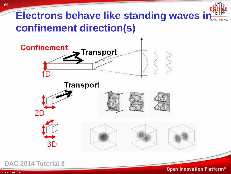
© 2011 TSMC, Ltd
TSMC Property
60
DAC 2014 Tutorial 8
Electrons behave like standing waves in
confinement direction(s)
© 2011 TSMC, Ltd
TSMC Property
61
DAC 2014 Tutorial 8
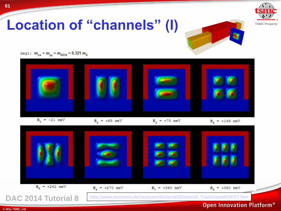
Location of “channels” (I)
http://www.nextnano.de/nextnano3/tutorial/2Dtutorial_TripleGateMOSFET.htm

© 2011 TSMC, Ltd
TSMC Property
62
DAC 2014 Tutorial 8
Small cross section
larger cross section
Location of “channels” (II) http://www.nextnano.de/nextnano3/tutorial/2Dtutorial_TripleGateMOSFET.htm

© 2011 TSMC, Ltd
TSMC Property
63
DAC 2014 Tutorial 8
Channel electron distribution vs. size
JP Colinge, “Quantum-wire effects in trigate
SOI MOSFETs”, Solid-State Electronics, Vol. 51,
pp. 1153–1160 (2007)
20nm x 20nm
10nm x 10nm
3nm x 3nm
5nm x 5nm
© 2011 TSMC, Ltd
TSMC Property
64
DAC 2014 Tutorial 8
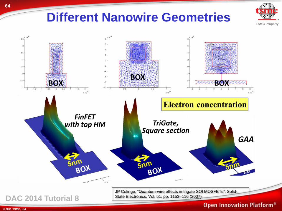
Different Nanowire Geometries
JP Colinge, “Quantum-wire effects in trigate SOI MOSFETs”, Solid-
State Electronics, Vol. 51, pp. 1153–116 (2007)

© 2011 TSMC, Ltd
TSMC Property
65
DAC 2014 Tutorial 8
ESSDERC 2012
Transition of Nanowire to Single-electron Transistor

© 2011 TSMC, Ltd
TSMC Property
66
DAC 2014 Tutorial 8
Can’t you really teach an old dog new tricks?
Old materials …. New properties?

© 2011 TSMC, Ltd
TSMC Property
67
DAC 2014 Tutorial 8
Nolan M, O'Callaghan S, Fagas G, Greer JC, Frauenheim T., “Silicon nanowire band gap modification”, Nano Lett. 2007 Jan;7(1):34-8.
Silicon
Band gap increases at small diameters

© 2011 TSMC, Ltd
TSMC Property
68
DAC 2014 Tutorial 8
Al
Sn
Cu Ag W
Tin is only twice as resistive as
tungsten!
From: http://www.webelements.com/
68

© 2011 TSMC, Ltd
TSMC Property
69
DAC 2014 Tutorial 8
Bulk Tin: metal
Nanowire Tin: semiconductor
Tin Band structure
L. Ansari, G. Fagas , J.P. Colinge , J.C. Greer , “A
Proposed Confinement Modulated Gap Nanowire
Transistor Based on a Metal (Tin), Nano Letters, Vol.
12 (5), pp 2222–2227 (2012)
© 2011 TSMC, Ltd
TSMC Property
70
DAC 2014 Tutorial 8
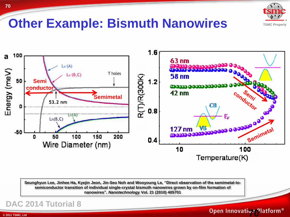
Seunghyun Lee, Jinhee Ha, Kyejin Jeon, Jin-Seo Noh and Wooyoung Le, “Direct observation of the semimetal-to-
semiconductor transition of individual single-crystal bismuth nanowires grown by on-film formation of
nanowires”, Nanotechnology Vol. 21 (2010) 405701
70
Semimetal
Semi
conductor
Other Example: Bismuth Nanowires
© 2011 TSMC, Ltd
TSMC Property
71
DAC 2014 Tutorial 8
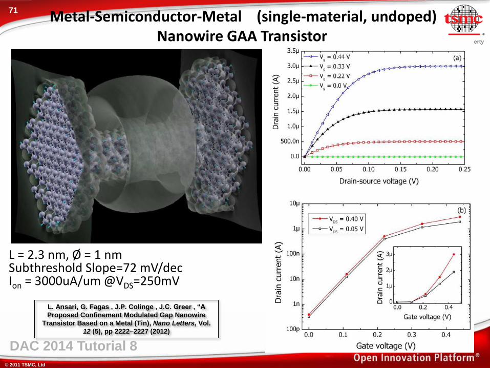
L = 2.3 nm, Ø = 1 nm Subthreshold Slope=72 mV/dec Ion = 3000uA/um @VDS=250mV
Metal-Semiconductor-Metal (single-material, undoped) Nanowire GAA Transistor
L. Ansari, G. Fagas , J.P. Colinge , J.C. Greer , “A
Proposed Confinement Modulated Gap Nanowire
Transistor Based on a Metal (Tin), Nano Letters, Vol.
12 (5), pp 2222–2227 (2012)

© 2011 TSMC, Ltd
TSMC Property
72
DAC 2014 Tutorial 8
Conclusions
A bit of history….. How did we get here?
Short-channel effects and multigate FETs
Nanowire transistor architectures
FinFET to NWT: Logic and SRAM applications
Modeling FinFET to NWT
Programmable devices and sensors in NWT
New Physics…Quantum Effects … New materials…
…Moore’s Law isn’t dead yet…


