63
RTL Hardware Design by P. Chu Chapter 10 1 Finite State Machines
RTL Hardware Design
by P. Chu
Chapter 10 1
Finite State Machines

RTL Hardware Design
by P. Chu
Chapter 10 2
Outline
1. Overview
2. FSM representation
3. Timing and performance of an FSM
4. Moore machine versus Mealy machine
5. VHDL description of FSMs
6. State assignment
7. Moore output buffering
8. FSM design examples

RTL Hardware Design
by P. Chu
Chapter 10 3
1. Overview on FSM
• Contain “random” logic in next-state logic
• Used mainly used as a controller in a large system
• Mealy vs Moore output

RTL Hardware Design
by P. Chu
Chapter 10 4
2. Representation of FSM
• State diagram

RTL Hardware Design
by P. Chu
Chapter 10 5
• E.g.
a memory
controller
• Signal not
asserted =
default
value

RTL Hardware Design
by P. Chu
Chapter 10 6
• ASM (algorithmic state machine) chart
– Flowchart-like diagram
– Provide the same info as an FSM
– More descriptive, better for complex
description
– ASM block
• One state box
• One ore more optional decision boxes: with T or F
exit path
• One or more conditional output boxes: for Mealy
output

RTL Hardware Design
by P. Chu
Chapter 10 7
RTL Hardware Design
by P. Chu
Chapter 10 8
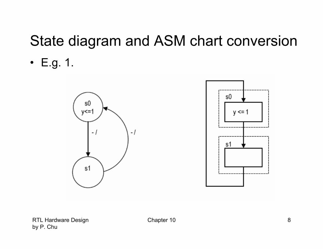
State diagram and ASM chart conversion
• E.g. 1.

RTL Hardware Design
by P. Chu
Chapter 10 9
• E.g. 2.

RTL Hardware Design
by P. Chu
Chapter 10 10
• E.g. 3.
RTL Hardware Design
by P. Chu
Chapter 10 11
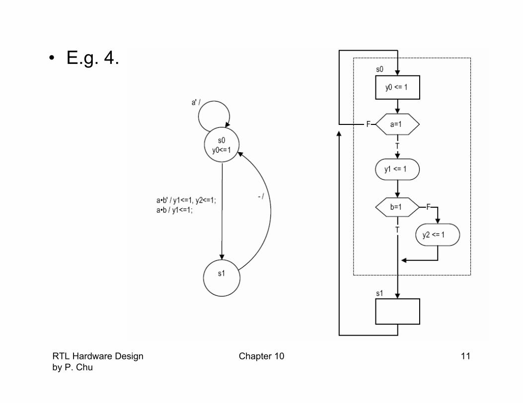
• E.g. 4.

RTL Hardware Design
by P. Chu
Chapter 10 12
• E.g. 6.

RTL Hardware Design
by P. Chu
Chapter 10 13
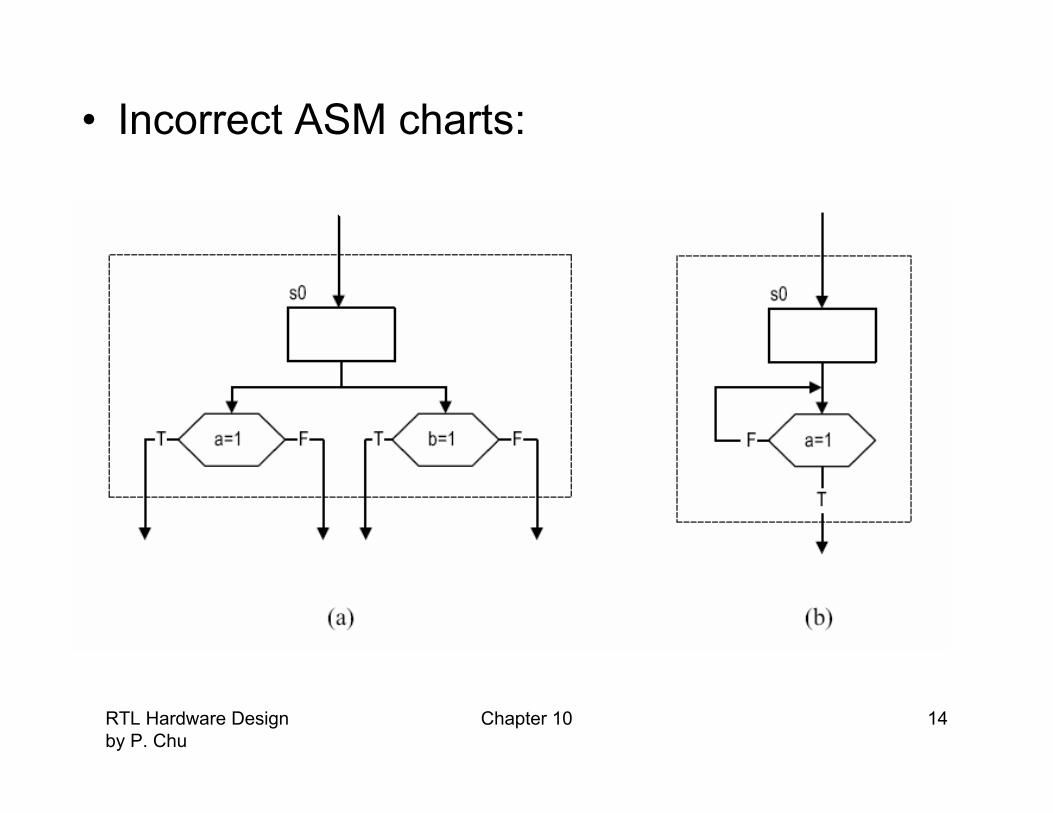
• Difference between a regular flowchart
and ASM chart:
– Transition governed by clock
– Transition done between ASM blocks
• Basic rules:
– For a given input combination, there is one
unique exit path from the current ASM block
– The exit path of an ASM block must always
lead to a state box. The state box can be the
state box of the current ASM block or a state
box of another ASM block.
RTL Hardware Design
by P. Chu
Chapter 10 14
• Incorrect ASM charts:

RTL Hardware Design
by P. Chu
Chapter 10 15

RTL Hardware Design
by P. Chu
Chapter 10 16
3. Performance of FSM
• Similar to regular sequential circuit
RTL Hardware Design
by P. Chu
Chapter 10 17
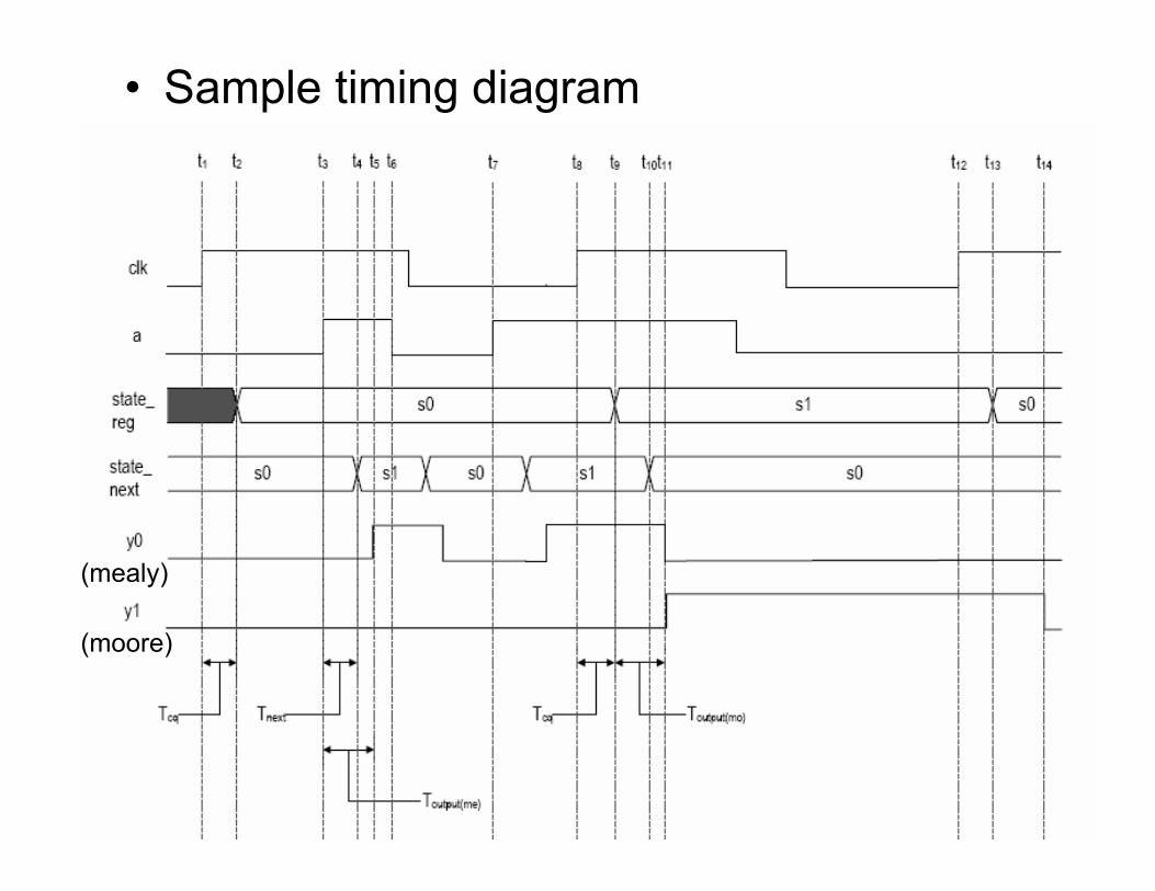
• Sample timing diagram
(mealy)
(moore)
RTL Hardware Design
by P. Chu
Chapter 10 18
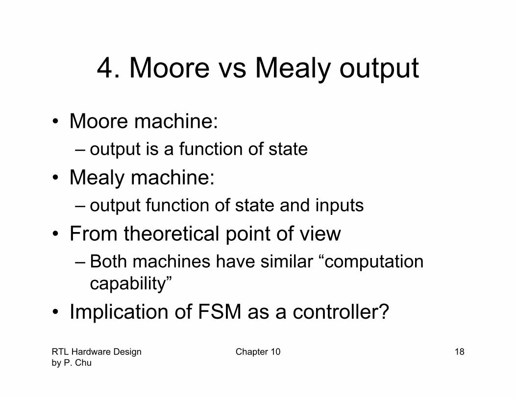
4. Moore vs Mealy output
• Moore machine:
– output is a function of state
• Mealy machine:
– output function of state and inputs
• From theoretical point of view
– Both machines have similar “computation
capability”
• Implication of FSM as a controller?

RTL Hardware Design
by P. Chu
Chapter 10 19
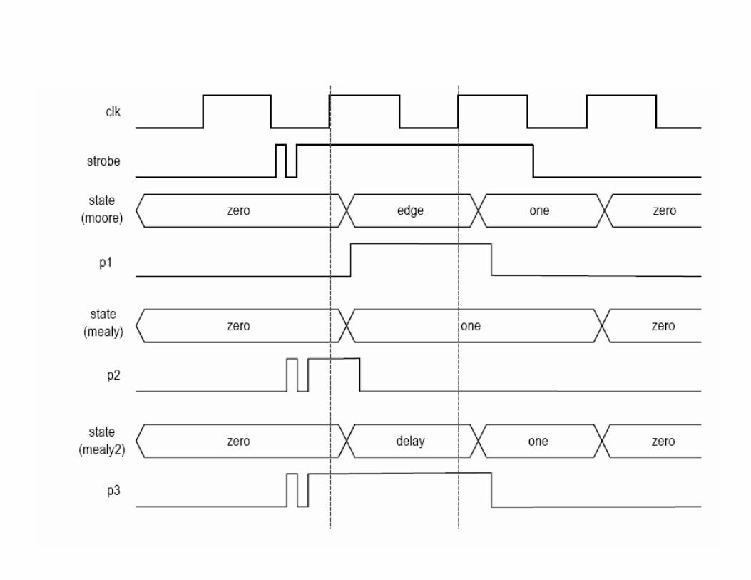
• E.g., edge detection circuit
– A circuit to detect the rising edge of a slow
“strobe” input and generate a “short”
(about 1-clock period) output pulse.

RTL Hardware Design
by P. Chu
Chapter 10 20
• Three designs:
RTL Hardware Design
by P. Chu
Chapter 10 21

RTL Hardware Design
by P. Chu
Chapter 10 22
• Comparison
– Mealy machine uses fewer states
– Mealy machine responds faster
– Mealy machine may be transparent to glitches
• Which one is better?
• Types of control signal
– Edge sensitive
• E.g., enable signal of counter
• Both can be used but Mealy is faster
– Level sensitive
• E.g., write enable signal of SRAM
• Moore is preferred
RTL Hardware Design
by P. Chu
Chapter 10 23
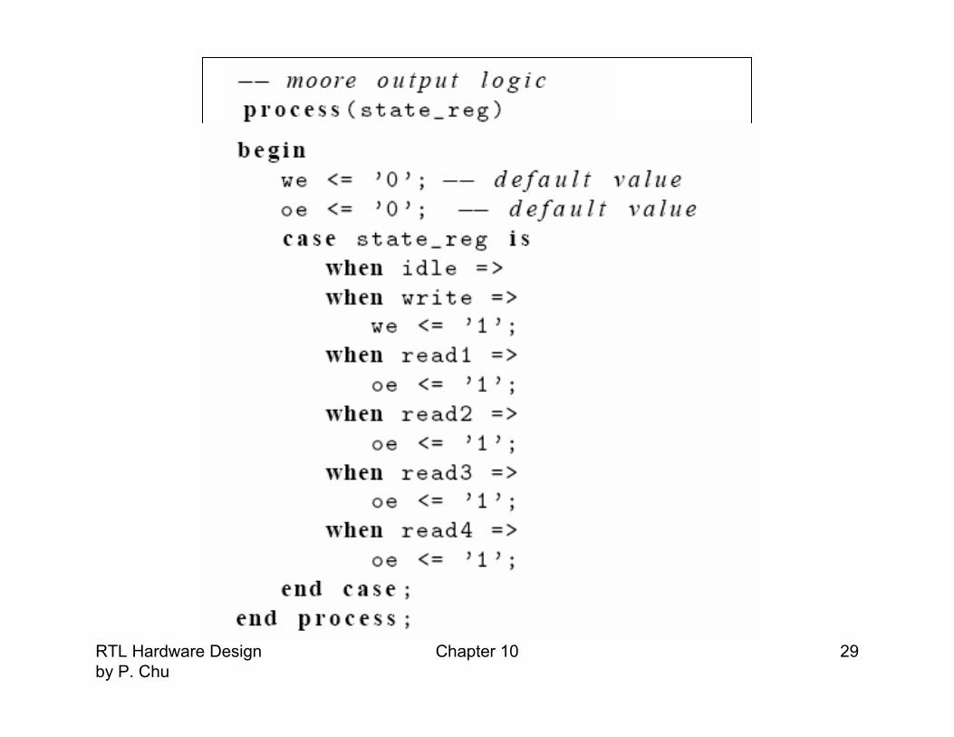
VHDL Description of FSM
• Follow the basic block diagram
• Code the next-state/output logic according
to the state diagram/ASM chart
• Use enumerate data type for states

RTL Hardware Design
by P. Chu
Chapter 10 24
• E.g. 6.

RTL Hardware Design
by P. Chu
Chapter 10 25

RTL Hardware Design
by P. Chu
Chapter 10 26

RTL Hardware Design
by P. Chu
Chapter 10 27

RTL Hardware Design
by P. Chu
Chapter 10 28
RTL Hardware Design
by P. Chu
Chapter 10 29
RTL Hardware Design
by P. Chu
Chapter 10 30

RTL Hardware Design
by P. Chu
Chapter 10 31
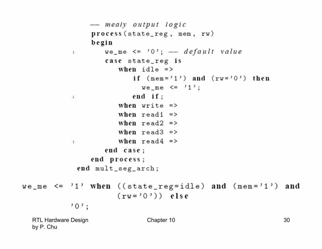
• Combine next-state/output logic together

RTL Hardware Design
by P. Chu
Chapter 10 32
RTL Hardware Design
by P. Chu
Chapter 10 33
RTL Hardware Design
by P. Chu
Chapter 10 34
6. State assignment
• State assignment: assign binary
representations to symbolic states
• In a synchronous FSM
– All assignments work
– Good assignment reduce the complexity of
next-state/output logic
• Typical assignment
– Binary, Gray, one-hot, almost one-hot

RTL Hardware Design
by P. Chu
Chapter 10 35
RTL Hardware Design
by P. Chu
Chapter 10 36
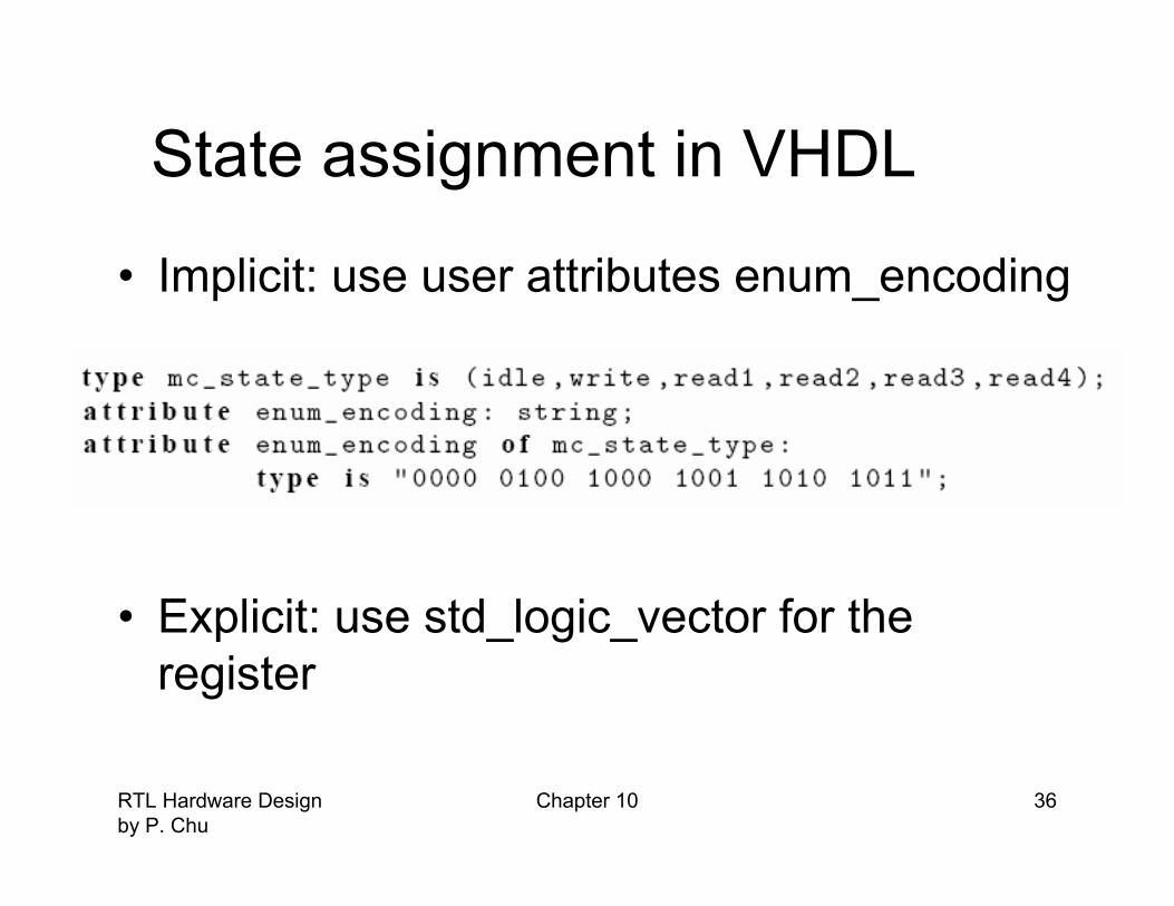
State assignment in VHDL
• Implicit: use user attributes enum_encoding
• Explicit: use std_logic_vector for the
register

RTL Hardware Design
by P. Chu
Chapter 10 37

RTL Hardware Design
by P. Chu
Chapter 10 38

RTL Hardware Design
by P. Chu
Chapter 10 39
Handling the unused state
• Many binary representations are not used
• What happens if the FSM enters an unused state?
– Ignore the condition
– Safe (Fault-tolerant) FSM: go to an error state or return to the initial state.
• Easy for the explicit state assignment
• No portable code for the enumerated data type

RTL Hardware Design
by P. Chu
Chapter 10 40
6. Moore output buffering
• FSM as control circuit
– Sometimes fast, glitch-free signal is needed
– An extra output buffer can be added, but
introduce one-clock delay
• Special schemes can be used for Moore
output
– Clever state assignment
– Look-ahead output circuit

RTL Hardware Design
by P. Chu
Chapter 10 41
• Potential problems of the Moore output
logic:
– Potential hazards introduce glitches
– Increase the Tco delay (Tco = Tcq + Toutput)
• Can we get control signals directly from
the register?

RTL Hardware Design
by P. Chu
Chapter 10 42
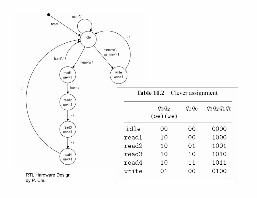
Clever state assignment
• Assigning state according to output signal
patterns
• Output can be obtained from register directly
• Extra register bits may be needed
• Must use explicit state assignment in VHDL
code to access individual register bit
• Difficult to revise and maintain
RTL Hardware Design
by P. Chu
Chapter 10 43

RTL Hardware Design
by P. Chu
Chapter 10 44
• VHDL code
RTL Hardware Design
by P. Chu
Chapter 10 45
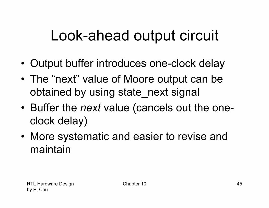
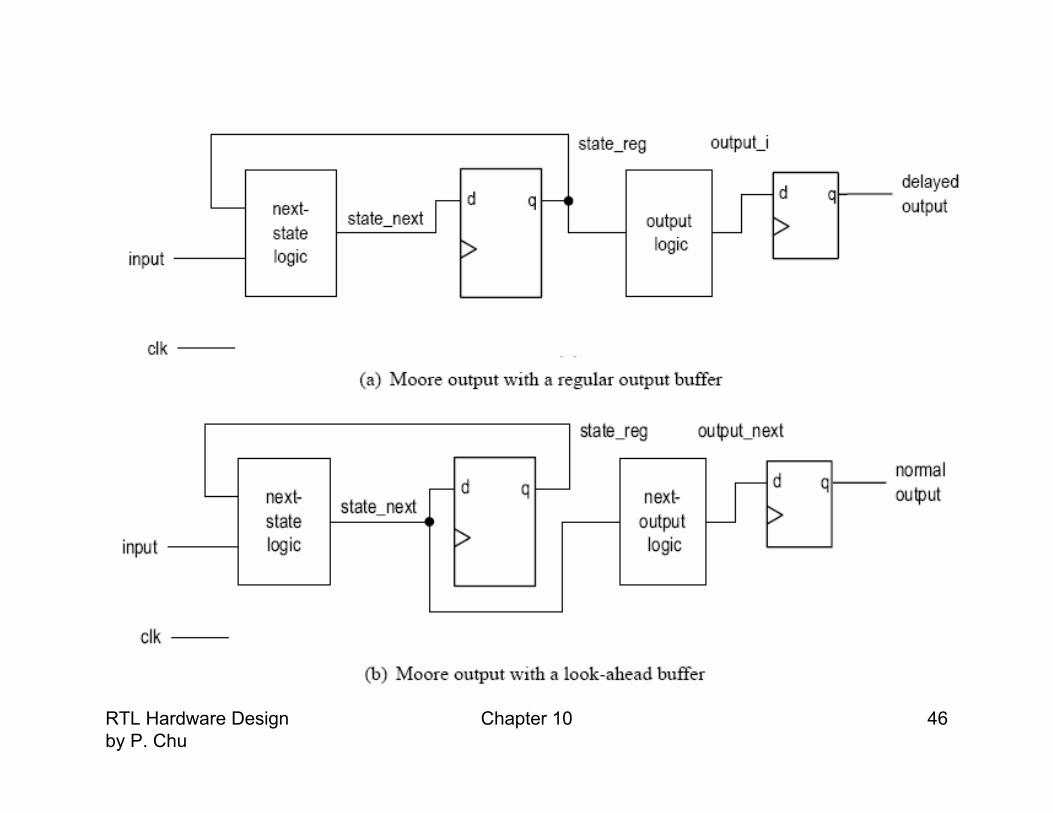
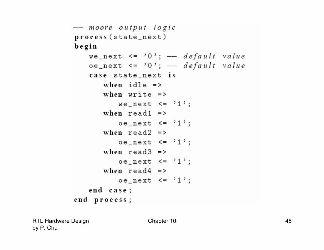
Look-ahead output circuit
• Output buffer introduces one-clock delay
• The “next” value of Moore output can be
obtained by using state_next signal
• Buffer the next value (cancels out the one-
clock delay)
• More systematic and easier to revise and
maintain
RTL Hardware Design
by P. Chu
Chapter 10 46
RTL Hardware Design
by P. Chu
Chapter 10 47
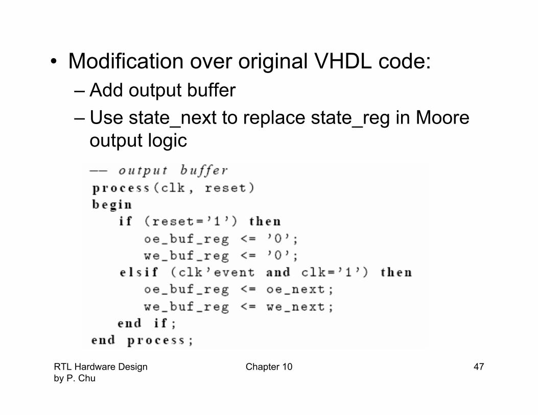
• Modification over original VHDL code:
– Add output buffer
– Use state_next to replace state_reg in Moore
output logic
RTL Hardware Design
by P. Chu
Chapter 10 48

RTL Hardware Design
by P. Chu
Chapter 10 49
7. FSM design examples
• Edge detector circuit
• Arbitrator (read)
• DRAM strobe signal generation
• Manchester encoding/decoding (read)
• FSM base binary counter

RTL Hardware Design
by P. Chu
Chapter 10 50
Edge detecting circuit (Moore)

RTL Hardware Design
by P. Chu
Chapter 10 51

RTL Hardware Design
by P. Chu
Chapter 10 52
Use clever state assignment
RTL Hardware Design
by P. Chu
Chapter 10 53
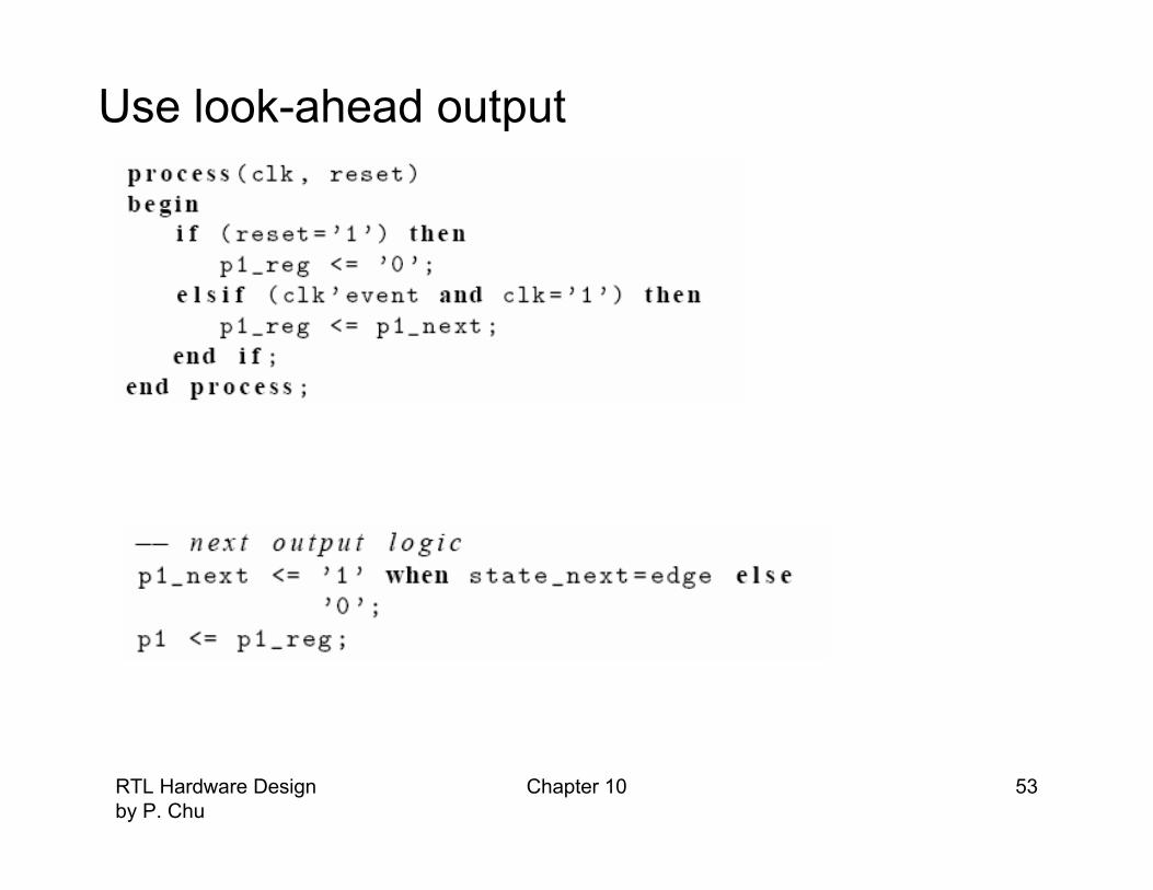
Use look-ahead output

RTL Hardware Design
by P. Chu
Chapter 10 54
Edge detecting circuit (Mealy)

RTL Hardware Design
by P. Chu
Chapter 10 55

RTL Hardware Design
by P. Chu
Chapter 10 56
• Edge detecting circuit (direct implementation):
– edge occurs when previous value is 0 and new
value is 1
– Same as Mealy design with state assignment:
zero => 0, one => 1

RTL Hardware Design
by P. Chu
Chapter 10 57
RTL Hardware Design
by P. Chu
Chapter 10 58
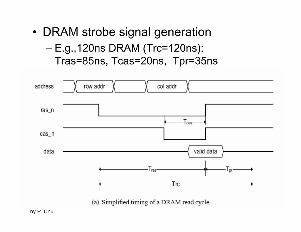
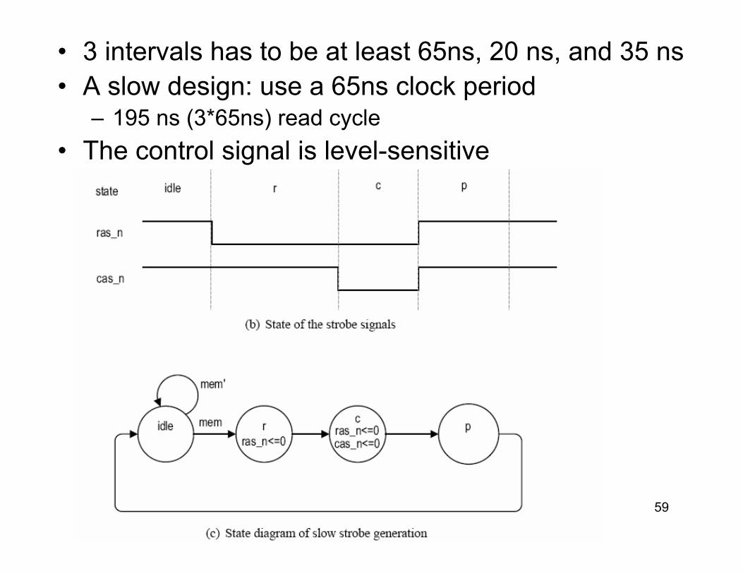
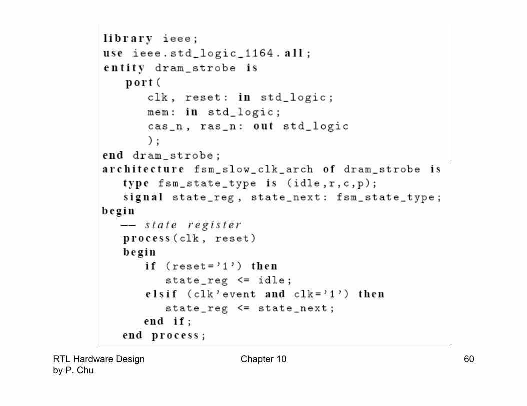
• DRAM strobe signal generation
– E.g.,120ns DRAM (Trc=120ns):
Tras=85ns, Tcas=20ns, Tpr=35ns
RTL Hardware Design
by P. Chu
Chapter 10 59
• 3 intervals has to be at least 65ns, 20 ns, and 35 ns
• A slow design: use a 65ns clock period – 195 ns (3*65ns) read cycle
• The control signal is level-sensitive
RTL Hardware Design
by P. Chu
Chapter 10 60

RTL Hardware Design
by P. Chu
Chapter 10 61
• Should revise the code to obtain glitch-free output

RTL Hardware Design
by P. Chu
Chapter 10 62
• A faster design: use a 20ns clock period
– 140 ns (7*20ns) read cycle
idle mem r1
ras_n<=0
p1cras_n<=0cas_n<=0
r2
ras_n<=0
r3
ras_n<=0
p2
mem'
r4
ras_n<=0
RTL Hardware Design
by P. Chu
Chapter 10 63
SummaryRepresenting FSMs
State Diagrams / ASM Charts
Timing and Performance
Moore/Mealy Outputs
Coding FSMs for Synthesis
Follow the block diagram: memory, ns/o logic
State assignment
Glitch-free Outputs: Clever, Buffering
FSM design examples


