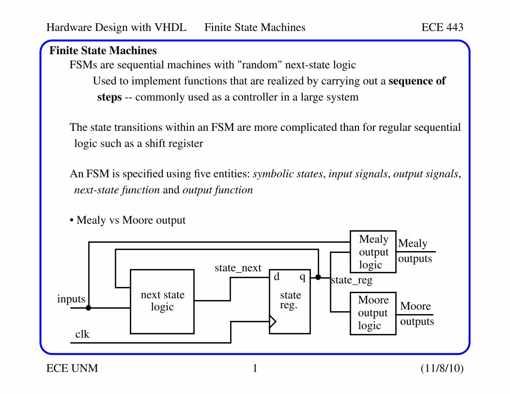
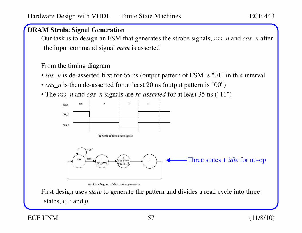
Hardware Design with VHDL Finite State Machines ECE 443 ECE UNM 1 (11/8/10) Finite State Machines FSMs are sequential machines with "random" next-state logic Used to implement functions that are realized by carrying out a sequence of steps -- commonly used as a controller in a large system The state transitions within an FSM are more complicated than for regular sequential logic such as a shift register An FSM is specified using five entities: symbolic states, input signals, output signals, next-state function and output function • Mealy vs Moore output next state state_next d q state clk Mealy inputs output Moore output logic logic Mealy outputs Moore outputs reg. logic state_reg
Transcript
Hardware Design with VHDL Finite State Machines ECE 443
ECE UNM 1 (11/8/10)
Finite State Machines
FSMs are sequential machines with "random" next-state logic
Used to implement functions that are realized by carrying out a sequence of
steps -- commonly used as a controller in a large system
The state transitions within an FSM are more complicated than for regular sequential
logic such as a shift register
An FSM is specified using five entities: symbolic states, input signals, output signals,
next-state function and output function
• Mealy vs Moore output
next state
state_nextd q
state
clk
Mealy
inputs
output
Mooreoutputlogic
logic
Mealy
outputs
Moore
outputs
reg.logic
state_reg
Hardware Design with VHDL Finite State Machines ECE 443
ECE UNM 2 (11/8/10)
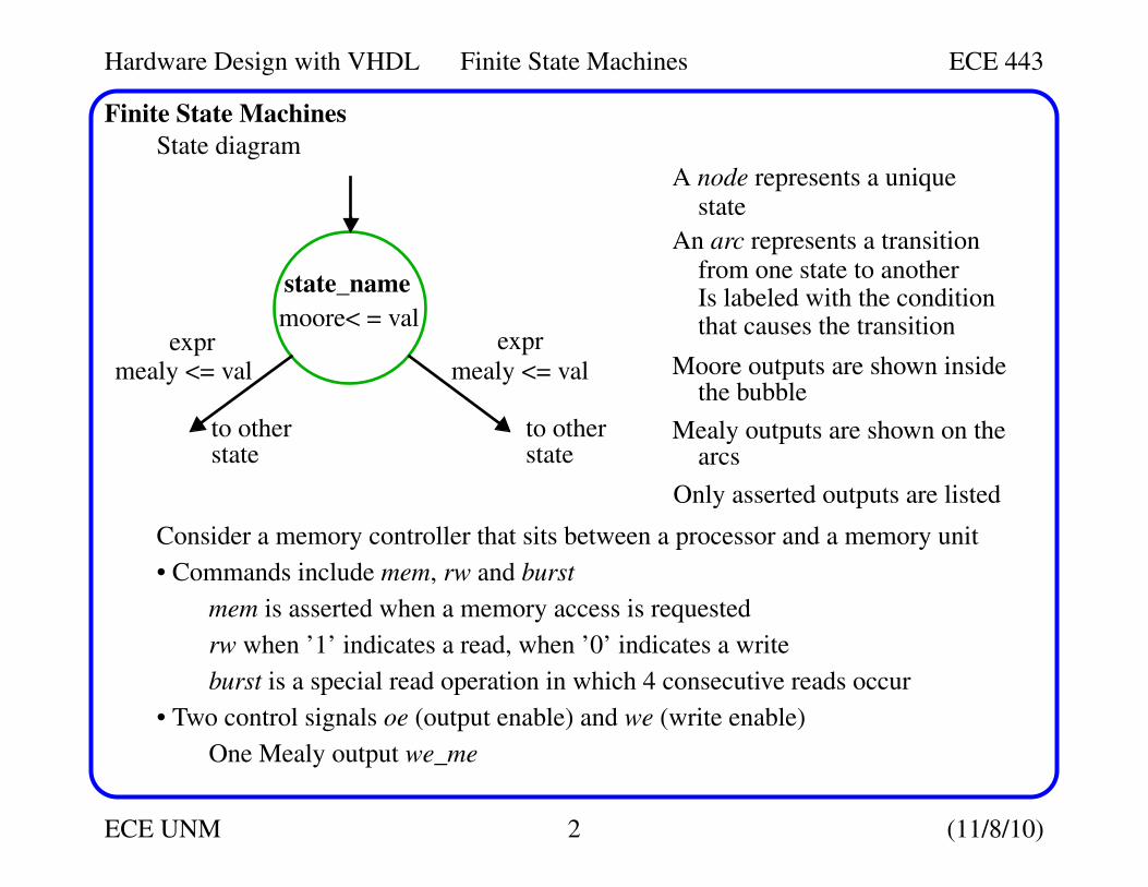
Finite State Machines
State diagram
Consider a memory controller that sits between a processor and a memory unit
• Commands include mem, rw and burst
mem is asserted when a memory access is requested
rw when ’1’ indicates a read, when ’0’ indicates a write
burst is a special read operation in which 4 consecutive reads occur
• Two control signals oe (output enable) and we (write enable)
One Mealy output we_me
A node represents a uniquestate
An arc represents a transitionfrom one state to anotherIs labeled with the conditionthat causes the transition
Moore outputs are shown insidethe bubble
Mealy outputs are shown on thearcs
Only asserted outputs are listed
state_name
moore< = valexpr
mealy <= val
expr
mealy <= val
to other to otherstatestate
Hardware Design with VHDL Finite State Machines ECE 443
ECE UNM 3 (11/8/10)
Finite State Machines
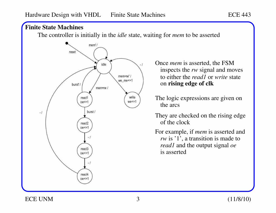
The controller is initially in the idle state, waiting for mem to be asserted
Once mem is asserted, the FSMinspects the rw signal and moves
to either the read1 or write state
The logic expressions are given onthe arcs
They are checked on the rising edgeof the clock
For example, if mem is asserted andrw is ’1’, a transition is made toread1 and the output signal oeis asserted
on rising edge of clk
Hardware Design with VHDL Finite State Machines ECE 443
ECE UNM 4 (11/8/10)
Finite State Machines
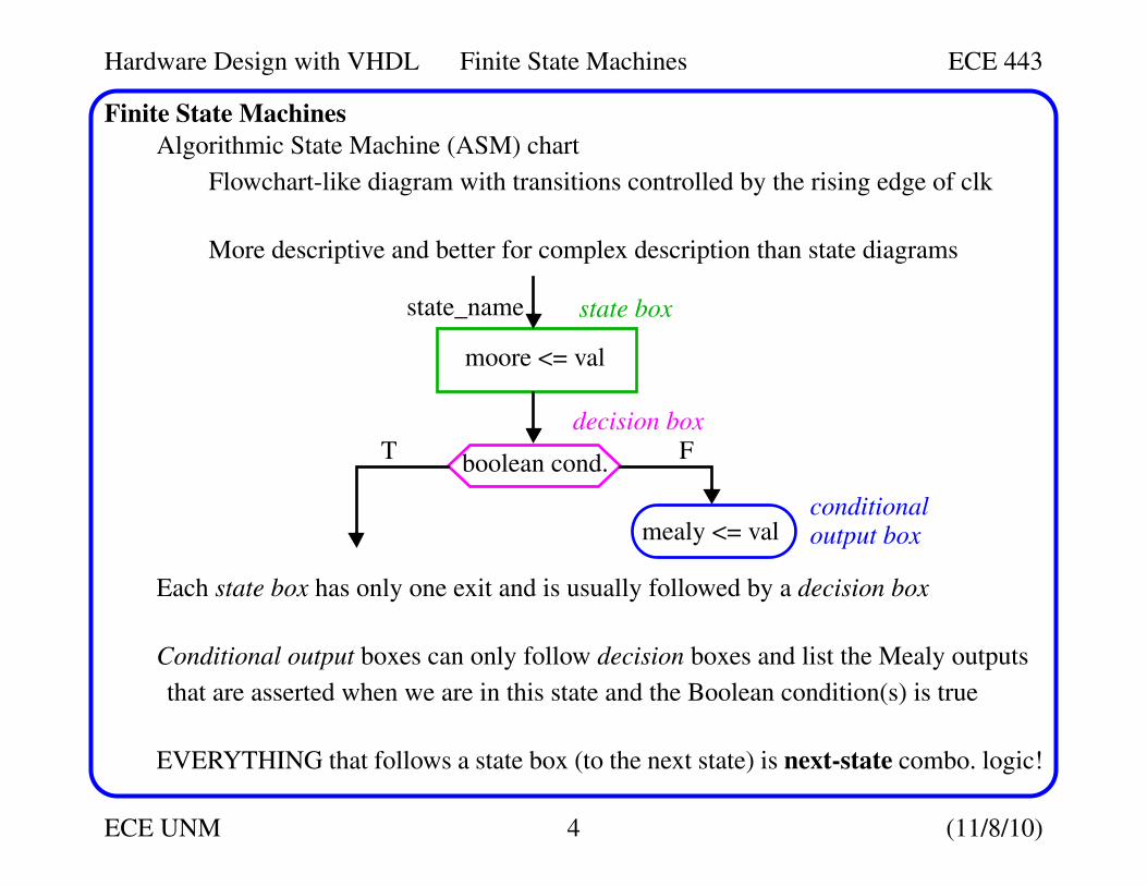
Algorithmic State Machine (ASM) chart
Flowchart-like diagram with transitions controlled by the rising edge of clk
More descriptive and better for complex description than state diagrams
Each state box has only one exit and is usually followed by a decision box
Conditional output boxes can only follow decision boxes and list the Mealy outputs
that are asserted when we are in this state and the Boolean condition(s) is true
EVERYTHING that follows a state box (to the next state) is next-state combo. logic!
moore <= val
state_name
boolean cond.T F
mealy <= valconditionaloutput box
decision box
state box
Hardware Design with VHDL Finite State Machines ECE 443
ECE UNM 5 (11/8/10)
Finite State Machines
Conversion between state diagrams and ASMs
Conversion process is trivial for the left example
For right example, a decision box is added to accommodate the conditional transition
to state s1 when a is true.
A conditional output box is added to handle the Mealy output that depends on both
state_reg=s0 and a=’1’
Hardware Design with VHDL Finite State Machines ECE 443
ECE UNM 6 (11/8/10)
Finite State Machines
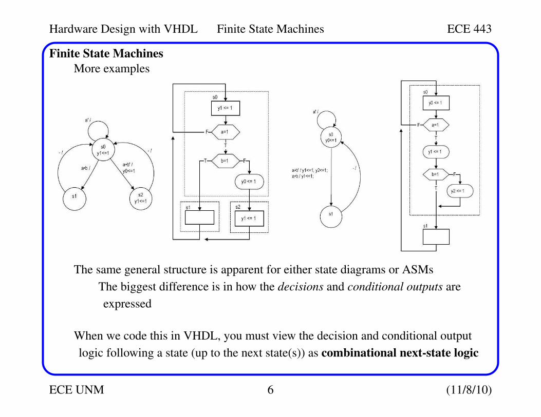
More examples
The same general structure is apparent for either state diagrams or ASMs
The biggest difference is in how the decisions and conditional outputs are
expressed
When we code this in VHDL, you must view the decision and conditional output
logic following a state (up to the next state(s)) as combinational next-state logic
Hardware Design with VHDL Finite State Machines ECE 443
ECE UNM 7 (11/8/10)
Finite State Machines
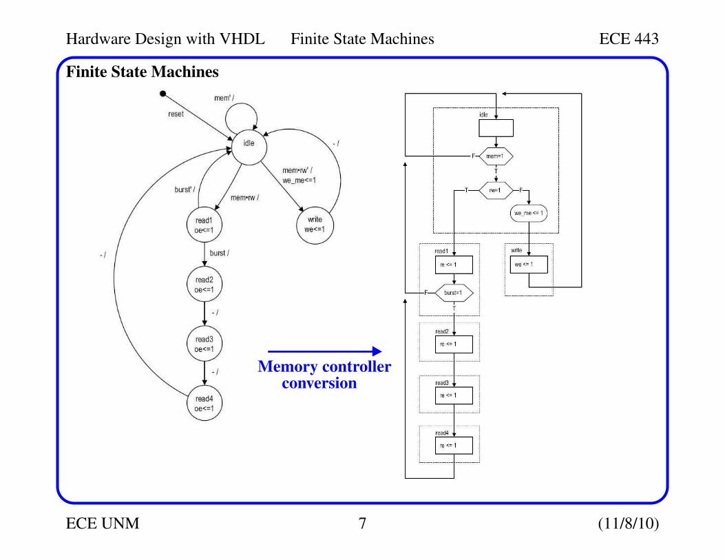
Memory controllerconversion
Hardware Design with VHDL Finite State Machines ECE 443
ECE UNM 8 (11/8/10)
Finite State Machines
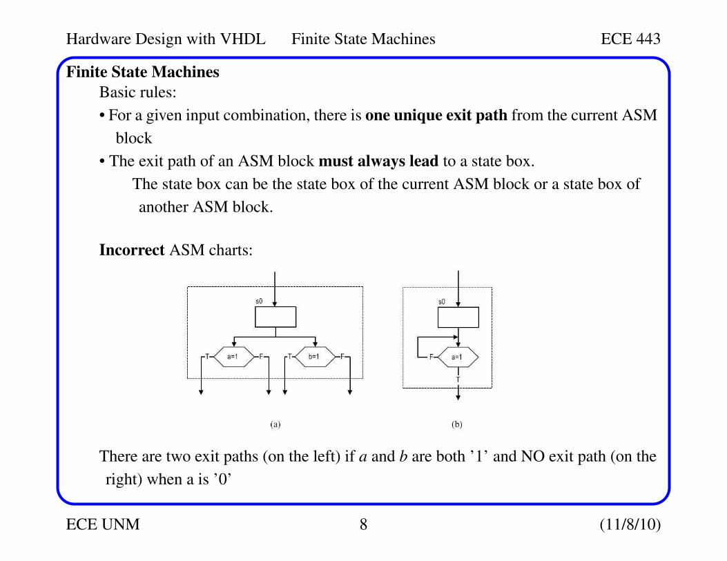
Basic rules:
• For a given input combination, there is one unique exit path from the current ASM
block
• The exit path of an ASM block must always lead to a state box.
The state box can be the state box of the current ASM block or a state box of
another ASM block.
Incorrect ASM charts:
There are two exit paths (on the left) if a and b are both ’1’ and NO exit path (on the
right) when a is ’0’
Hardware Design with VHDL Finite State Machines ECE 443
ECE UNM 9 (11/8/10)
Finite State Machines
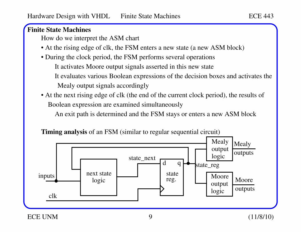
How do we interpret the ASM chart
• At the rising edge of clk, the FSM enters a new state (a new ASM block)
• During the clock period, the FSM performs several operations
It activates Moore output signals asserted in this new state
It evaluates various Boolean expressions of the decision boxes and activates the
Mealy output signals accordingly
• At the next rising edge of clk (the end of the current clock period), the results of
Boolean expression are examined simultaneously
An exit path is determined and the FSM stays or enters a new ASM block
Timing analysis of an FSM (similar to regular sequential circuit)
next state
state_nextd q
state
clk
Mealy
inputs
output
Mooreoutputlogic
logic
Mealy
outputs
Moore
outputs
reg.logic
state_reg
Hardware Design with VHDL Finite State Machines ECE 443
ECE UNM 10 (11/8/10)
Timing Analysis of FSMs
Consider a circuit with both a Moore and Mealy output
The timing parameters are
• Tcq, Tsetup, Thold, Tnext(max)
• Toutput(mo) (Moore logic) and Toutput(me) (Mealy logic)
Similar to the analysis of a regular sequential circuit, the minimum clock period (max
clk freq) of a FSM is given by
Tc = Tcq + Tnext(max) + Tsetup
Hardware Design with VHDL Finite State Machines ECE 443
ECE UNM 11 (11/8/10)
Timing Analysis of FSMs
Sample timing diagram
Hardware Design with VHDL Finite State Machines ECE 443
ECE UNM 12 (11/8/10)
Timing Analysis of FSMs
Since the FSM is frequently used in a controller application, the delay of the output
signals are important
For Moore
Tco(mo) = Tcq + Toutput(mo)
For Mealy (when change is due to a change in state)
Tco(me) = Tcq + Toutput(me)
For Mealy (when change is due to a change in input signal(s))
Tco(me) = Toutput(me)
Although the difference between a Moore and Mealy output seem subtle, as you can
see from the timing diagram, there behaviors can be very different
And, in general, it takes fewer states to realize a given function using a Mealy
machine (note that both are equivalent in ’power’)
But greater care must be exercised
Hardware Design with VHDL Finite State Machines ECE 443
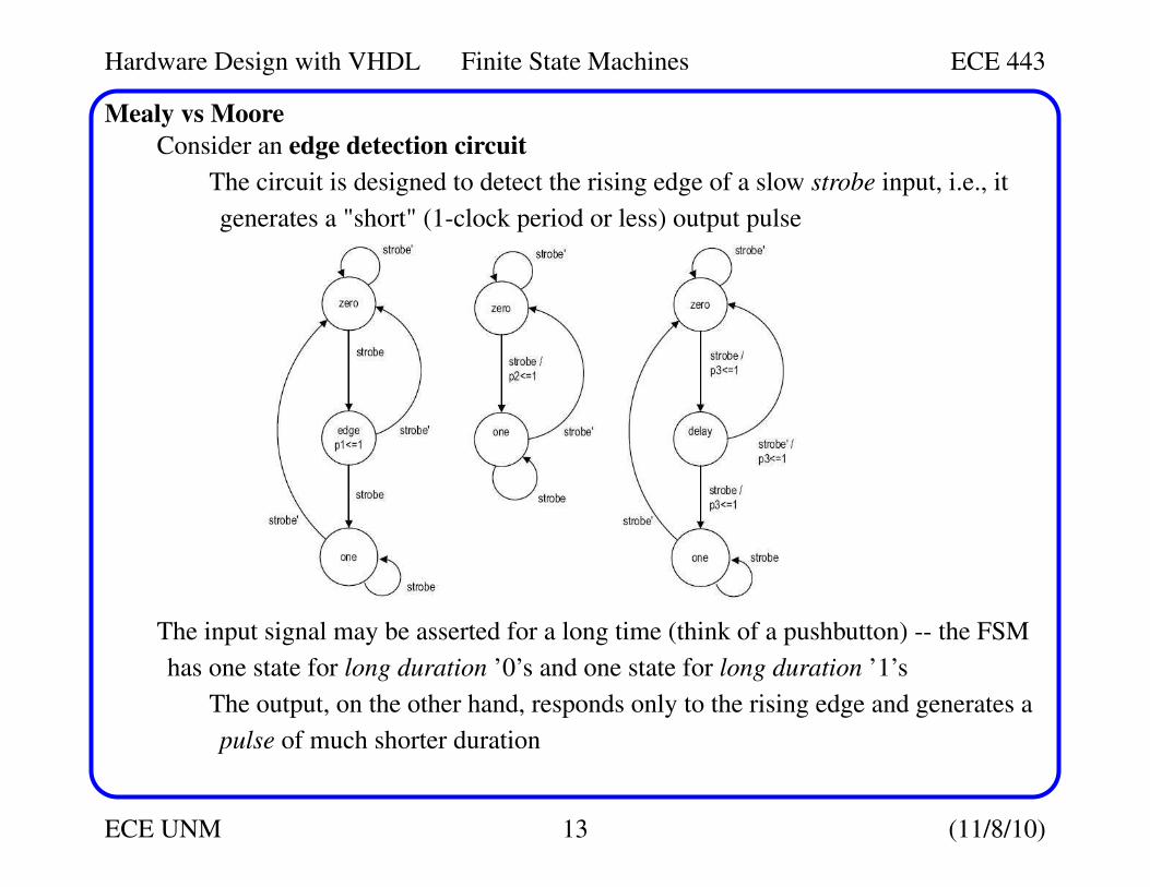
ECE UNM 13 (11/8/10)
Mealy vs Moore
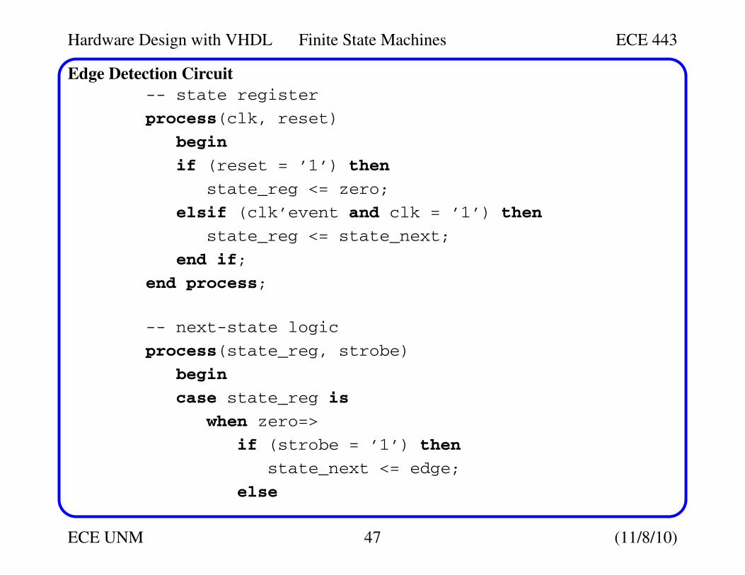
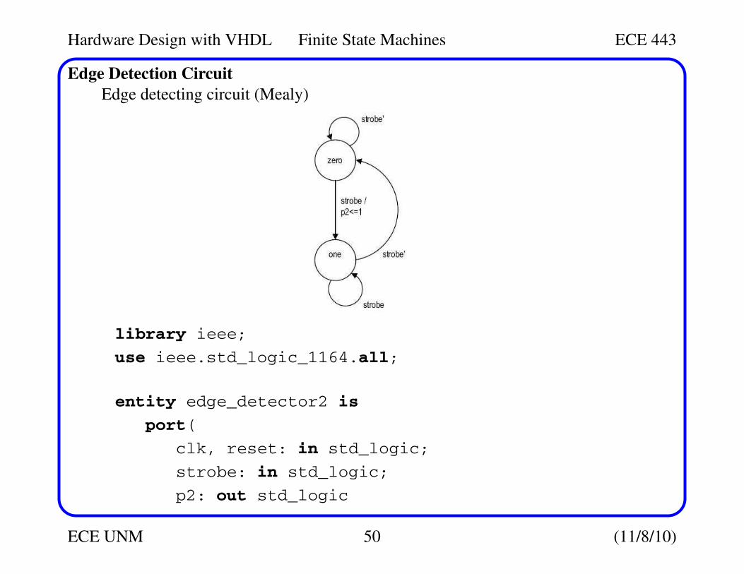
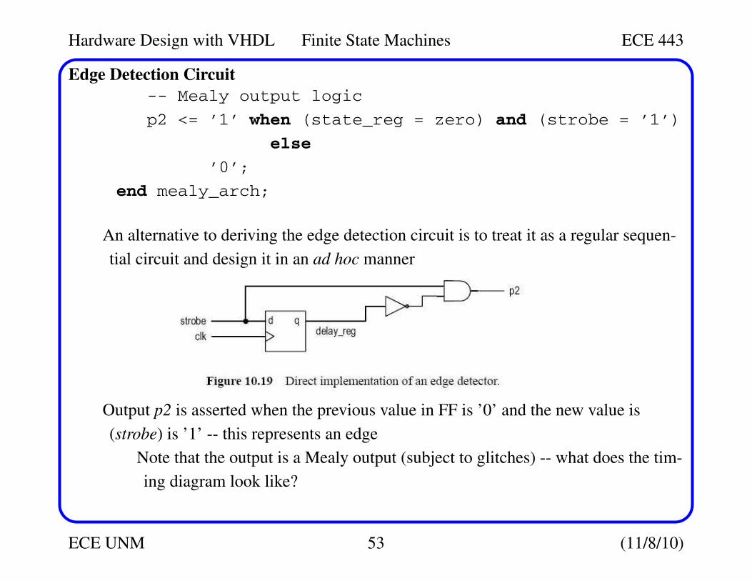
Consider an edge detection circuit
The circuit is designed to detect the rising edge of a slow strobe input, i.e., it
generates a "short" (1-clock period or less) output pulse
The input signal may be asserted for a long time (think of a pushbutton) -- the FSM
has one state for long duration ’0’s and one state for long duration ’1’s
The output, on the other hand, responds only to the rising edge and generates a
pulse of much shorter duration
Hardware Design with VHDL Finite State Machines ECE 443
ECE UNM 14 (11/8/10)
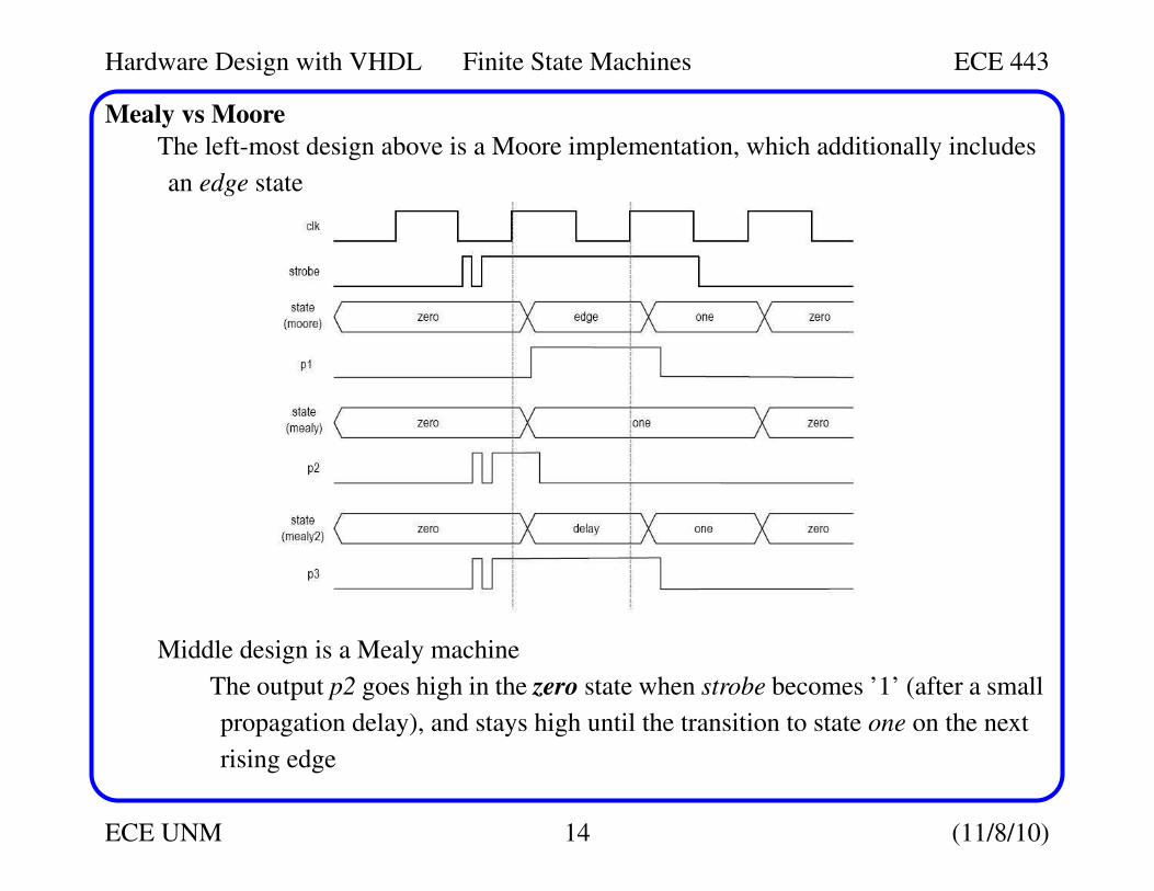
Mealy vs Moore
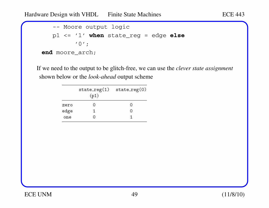
The left-most design above is a Moore implementation, which additionally includes
an edge state
Middle design is a Mealy machine
The output p2 goes high in the zero state when strobe becomes ’1’ (after a small
propagation delay), and stays high until the transition to state one on the next
rising edge
Hardware Design with VHDL Finite State Machines ECE 443
ECE UNM 15 (11/8/10)
Mealy vs Moore
The right-most design includes both types of outputs and adds a third state delay
The state diagram asserts p3 in the zero state (as in second version) when strobe
goes high and transitions to delay state
But since both transitions out of the delay state keep p2 asserted, this has the
effect of adding a clock cycle to p2’s high state (as in the first version)
Since the assertion is on all outgoing arcs, it is high independent of the input
conditions (and can be added inside the bubble as a Moore output)
All three designs generate a ’shot pulse’ but with subtle differences -- understanding
these differences is key to deriving a correct and efficient FSM
There are three main differences between Mealy and Moore:
• Mealy machine uses fewer states -- the input dependency allows several output val-
ues to be specified in the same state
• Mealy machine responds faster -- one clock cycle earlier in systems that use output
• Mealy machine may be transparent to glitches, i.e., passing them to the output
Hardware Design with VHDL Finite State Machines ECE 443
ECE UNM 16 (11/8/10)
Mealy vs Moore
So which one is better?
For control system applications, we can divide control signals into two categories,
edge sensitive and level sensitive
An edge sensitive signal (e.g., the enable signal on a counter) is sampled only on the
rising edge of clock
Therefore, glitches do NOT matter -- only the setup and hold times must be
obeyed
Both Mealy and Moore machines can generate output signals that meet this require-
ment
However, Mealy machines are preferred because it responds one clk cycle faster
and uses fewer states
For a level sensitive control signal, the signal must be asserted for a certain interval
of time (e.g., the write enable signal of an SRAM chip) and Moore is preferred
While asserted, it MUST remain stable and free of glitches
Hardware Design with VHDL Finite State Machines ECE 443
ECE UNM 17 (11/8/10)
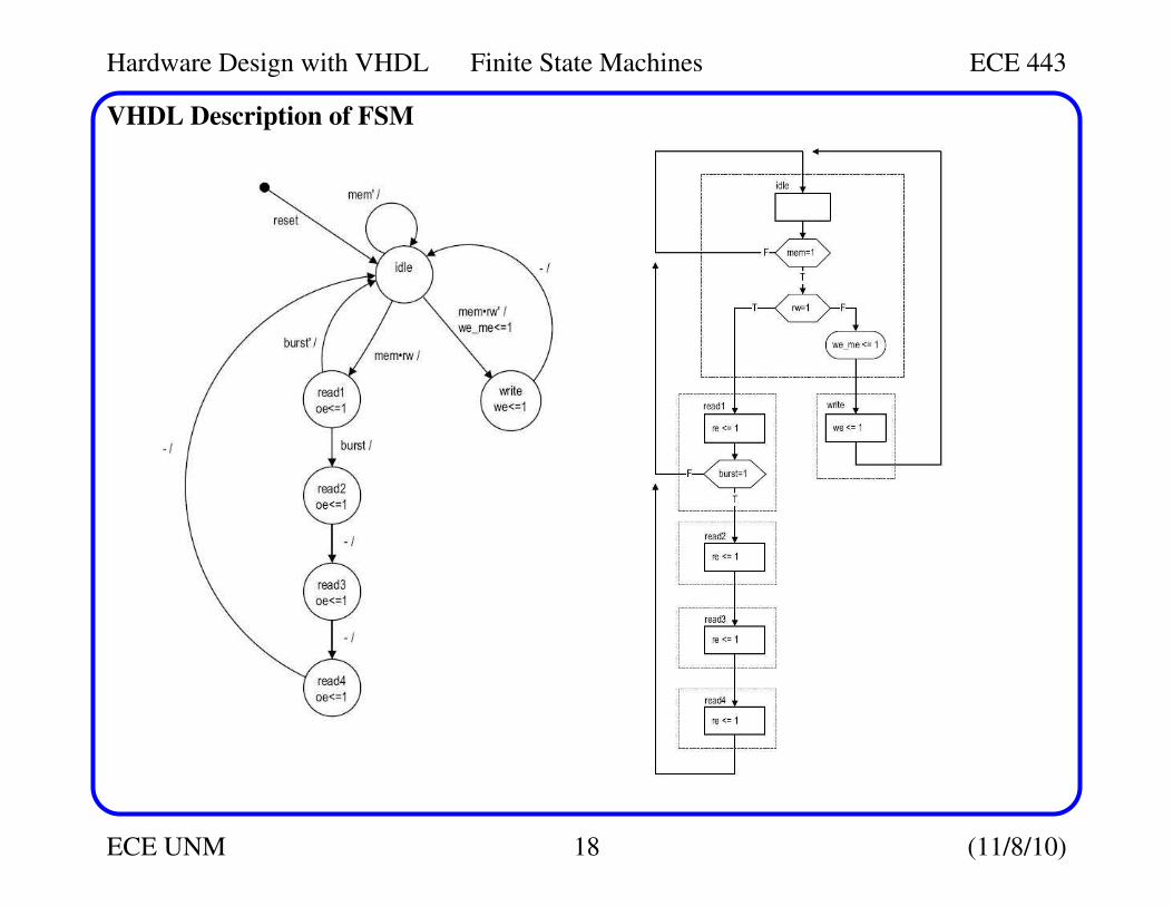
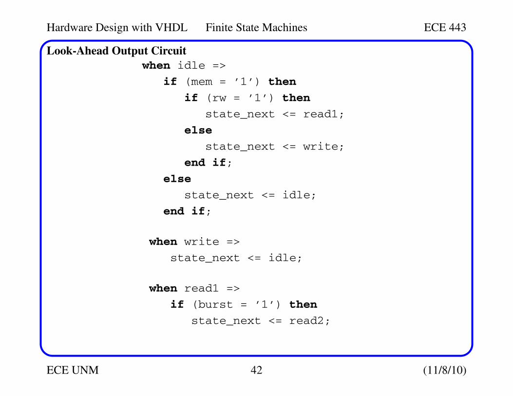
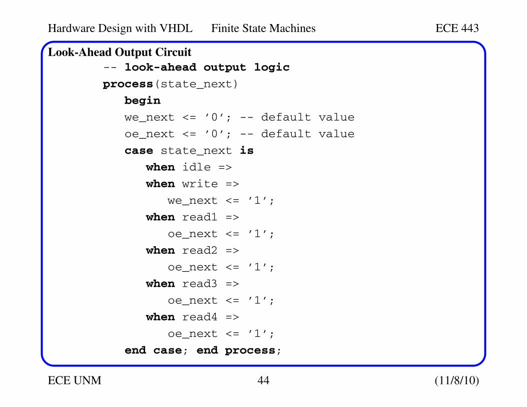
VHDL Description of FSM
Coding FSMs is similar to regular sequential logic, e.g., separate the memory ele-
ments out and derive the next-state/output logic
There are two differences
• Symbolic states are used in an FSM description -- we use the enumeration VHDL
data type for the state registers
• The next-state logic needs to be constructed according to a state diagram or ASM,
as opposed to using regular combinational logic such as a incrementer or shifter
There are several coding styles
• Multi-Segment: Create a VHDL code segment for each block in the block diagram
Memorycontrollerexample
Hardware Design with VHDL Finite State Machines ECE 443
ECE UNM 18 (11/8/10)
VHDL Description of FSM
Hardware Design with VHDL Finite State Machines ECE 443
ECE UNM 19 (11/8/10)
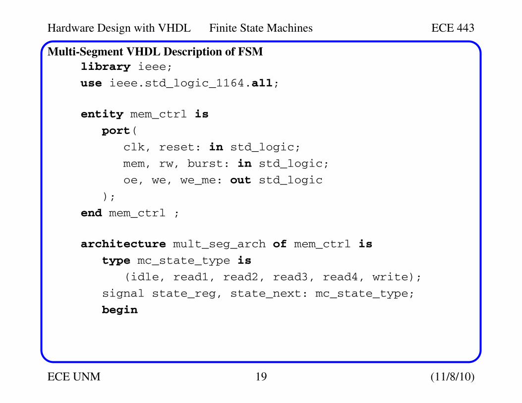
Multi-Segment VHDL Description of FSM
library ieee;
use ieee.std_logic_1164.all;
entity mem_ctrl is
port(
clk, reset: in std_logic;
mem, rw, burst: in std_logic;
oe, we, we_me: out std_logic
);
end mem_ctrl ;
architecture mult_seg_arch of mem_ctrl is
type mc_state_type is
(idle, read1, read2, read3, read4, write);
signal state_reg, state_next: mc_state_type;
begin
Hardware Design with VHDL Finite State Machines ECE 443
ECE UNM 20 (11/8/10)
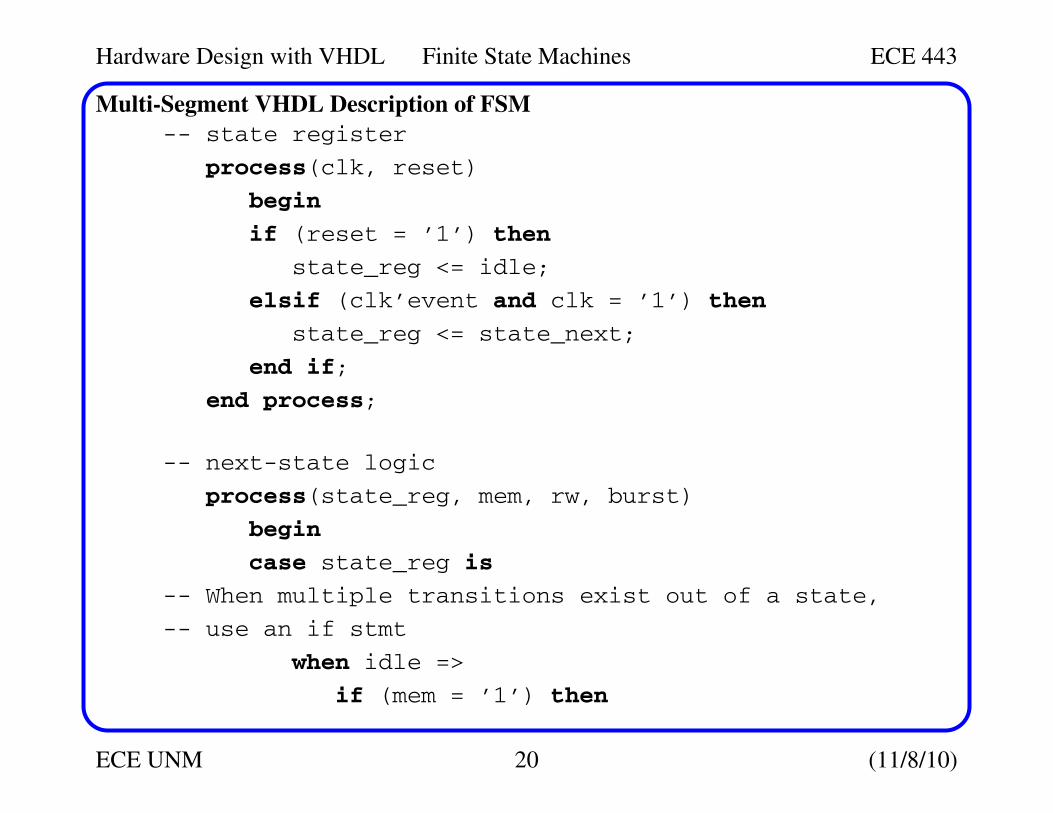
Multi-Segment VHDL Description of FSM
-- state register
process(clk, reset)
begin
if (reset = ’1’) then
state_reg <= idle;
elsif (clk’event and clk = ’1’) then
state_reg <= state_next;
end if;
end process;
-- next-state logic
process(state_reg, mem, rw, burst)
begin
case state_reg is
-- When multiple transitions exist out of a state,
-- use an if stmt
when idle =>
if (mem = ’1’) then
Hardware Design with VHDL Finite State Machines ECE 443
ECE UNM 21 (11/8/10)
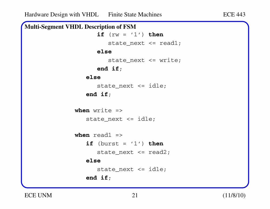
Multi-Segment VHDL Description of FSM
if (rw = ’1’) then
state_next <= read1;
else
state_next <= write;
end if;
else
state_next <= idle;
end if;
when write =>
state_next <= idle;
when read1 =>
if (burst = ’1’) then
state_next <= read2;
else
state_next <= idle;
end if;
Hardware Design with VHDL Finite State Machines ECE 443
ECE UNM 22 (11/8/10)
Multi-Segment VHDL Description of FSM
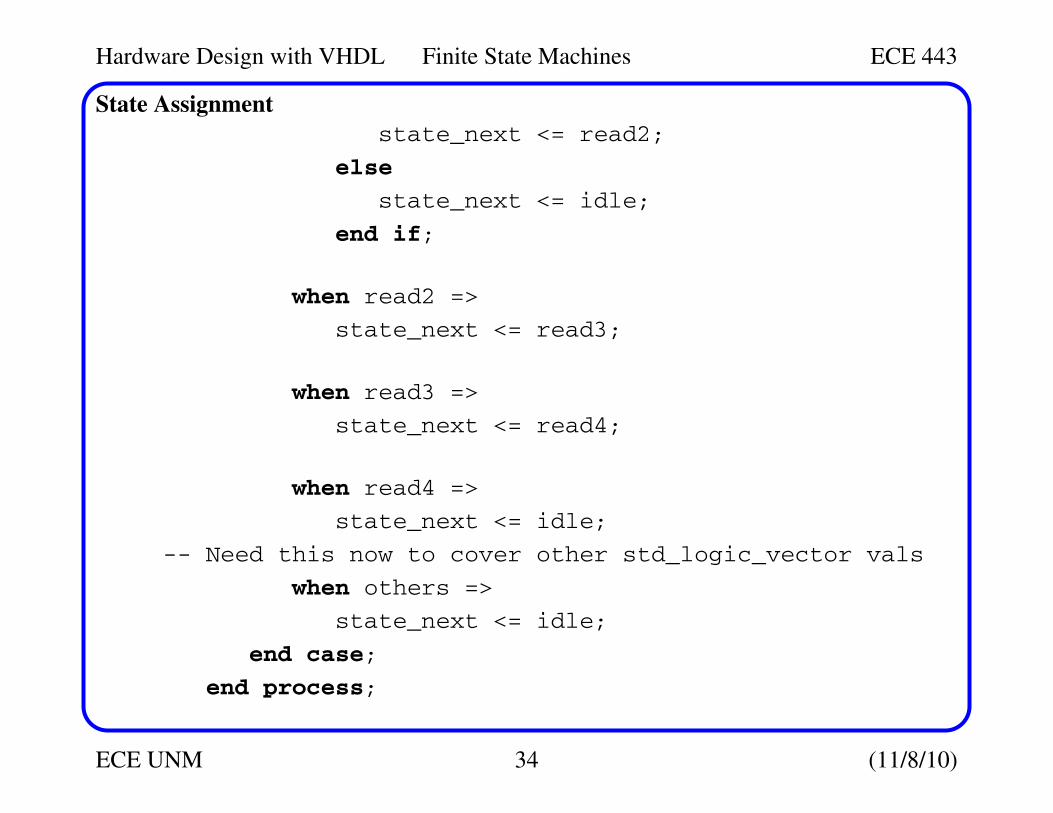
when read2 =>
state_next <= read3;
when read3 =>
state_next <= read4;
when read4 =>
state_next <= idle;
end case;
end process;
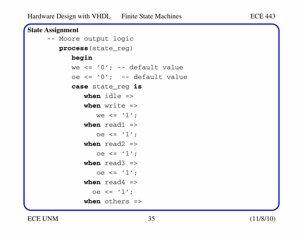
-- Moore output logic
process(state_reg)
begin
we <= ’0’; -- default value
oe <= ’0’; -- default value
Hardware Design with VHDL Finite State Machines ECE 443
ECE UNM 23 (11/8/10)
Multi-Segment VHDL Description of FSM
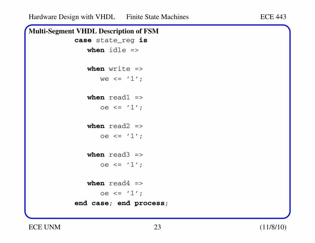
case state_reg is
when idle =>
when write =>
we <= ’1’;
when read1 =>
oe <= ’1’;
when read2 =>
oe <= ’1’;
when read3 =>
oe <= ’1’;
when read4 =>
oe <= ’1’;
end case; end process;
Hardware Design with VHDL Finite State Machines ECE 443
ECE UNM 24 (11/8/10)
Multi-Segment VHDL Description of FSM
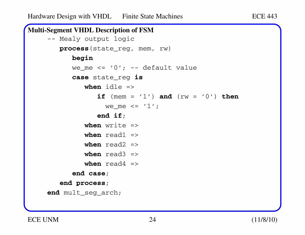
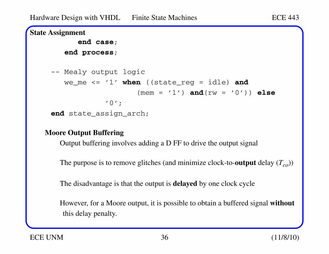
-- Mealy output logic
process(state_reg, mem, rw)
begin
we_me <= ’0’; -- default value
case state_reg is
when idle =>
if (mem = ’1’) and (rw = ’0’) then
we_me <= ’1’;
end if;
when write =>
when read1 =>
when read2 =>
when read3 =>
when read4 =>
end case;
end process;
end mult_seg_arch;
Hardware Design with VHDL Finite State Machines ECE 443
ECE UNM 25 (11/8/10)
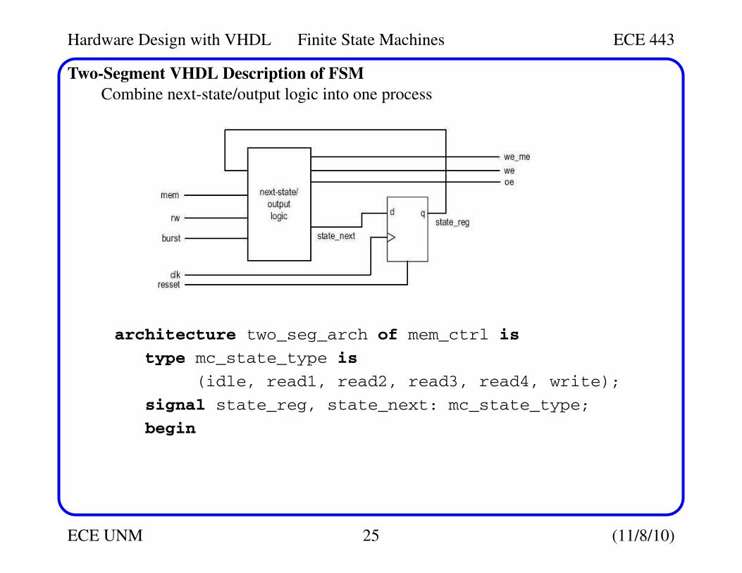
Two-Segment VHDL Description of FSM
Combine next-state/output logic into one process
architecture two_seg_arch of mem_ctrl is
type mc_state_type is
(idle, read1, read2, read3, read4, write);
signal state_reg, state_next: mc_state_type;
begin
Hardware Design with VHDL Finite State Machines ECE 443
ECE UNM 26 (11/8/10)
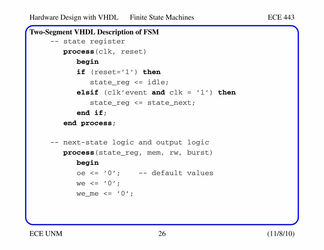
Two-Segment VHDL Description of FSM
-- state register
process(clk, reset)
begin
if (reset=’1’) then
state_reg <= idle;
elsif (clk’event and clk = ’1’) then
state_reg <= state_next;
end if;
end process;
-- next-state logic and output logic
process(state_reg, mem, rw, burst)
begin
oe <= ’0’; -- default values
we <= ’0’;
we_me <= ’0’;
Hardware Design with VHDL Finite State Machines ECE 443
ECE UNM 27 (11/8/10)
Two-Segment VHDL Description of FSM
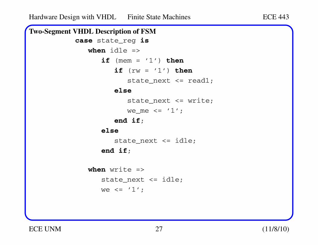
case state_reg is
when idle =>
if (mem = ’1’) then
if (rw = ’1’) then
state_next <= read1;
else
state_next <= write;
we_me <= ’1’;
end if;
else
state_next <= idle;
end if;
when write =>
state_next <= idle;
we <= ’1’;
Hardware Design with VHDL Finite State Machines ECE 443
ECE UNM 28 (11/8/10)
Two-Segment VHDL Description of FSM
when read1 =>
if (burst=’1’) then
state_next <= read2;
else
state_next <= idle;
end if;
oe <= ’1’;
when read2 =>
state_next <= read3;
oe <= ’1’;
when read3 =>
state_next <= read4;
oe <= ’1’;
Hardware Design with VHDL Finite State Machines ECE 443
ECE UNM 29 (11/8/10)
Two-Segment VHDL Description of FSM
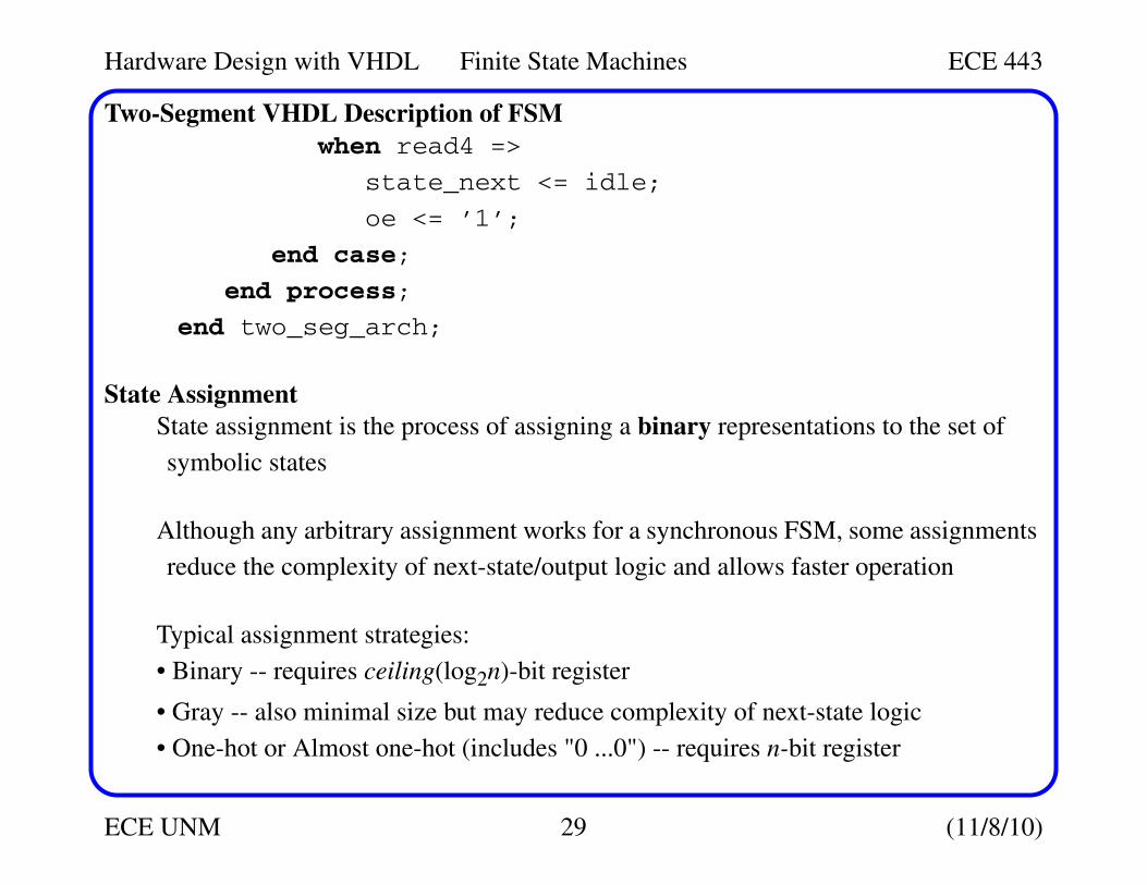
when read4 =>
state_next <= idle;
oe <= ’1’;
end case;
end process;
end two_seg_arch;
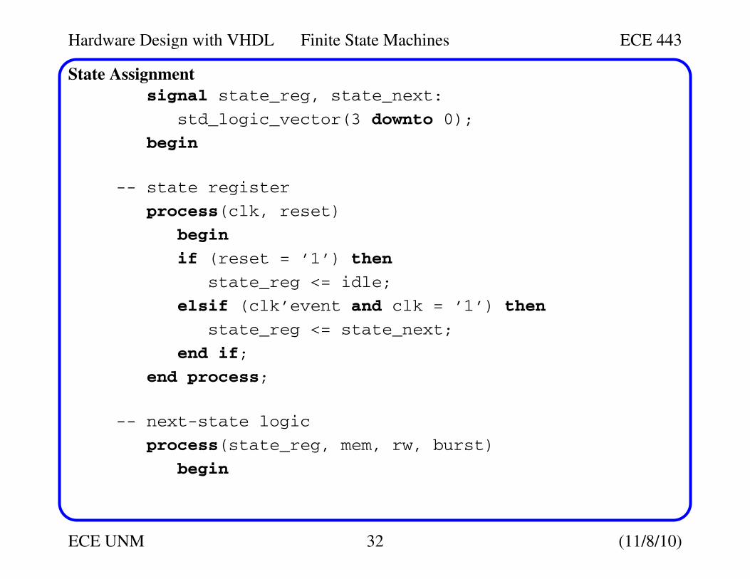
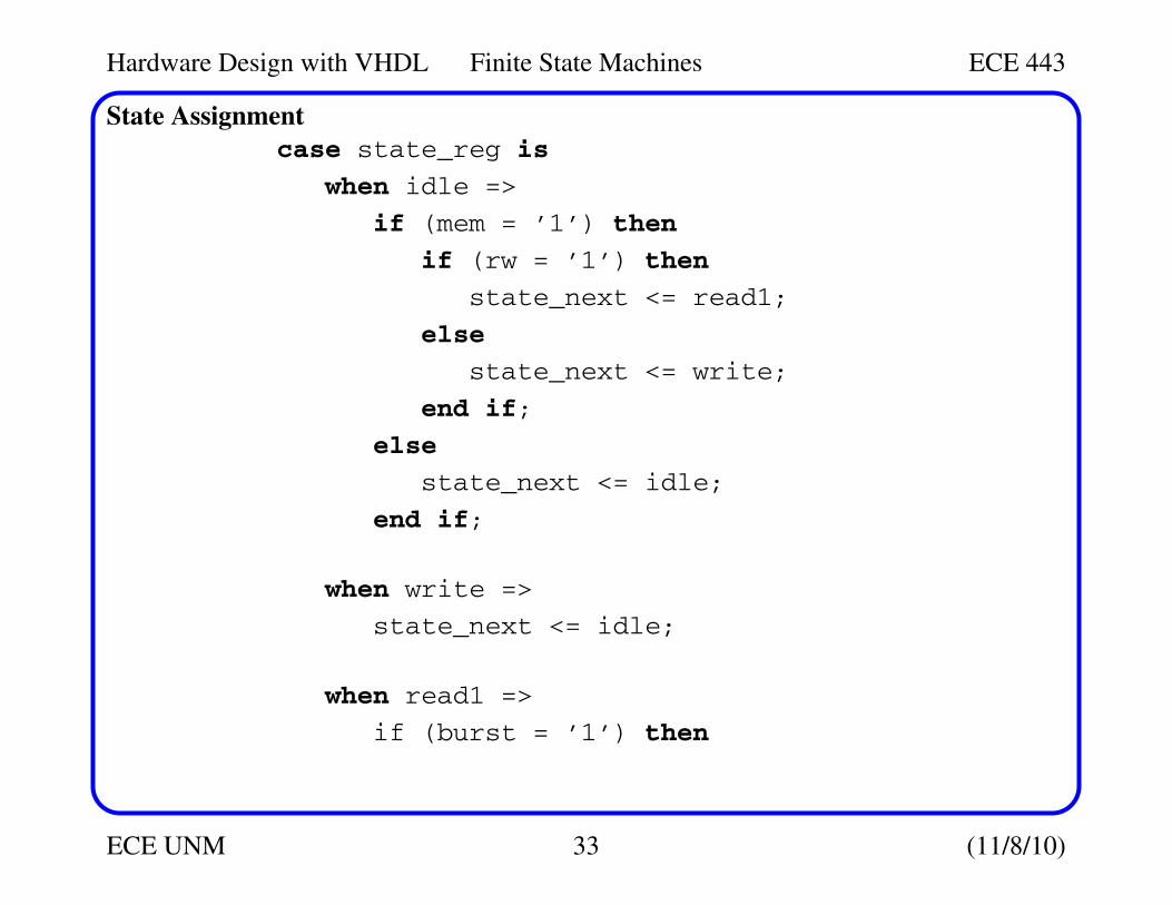
State Assignment
State assignment is the process of assigning a binary representations to the set of
symbolic states
Although any arbitrary assignment works for a synchronous FSM, some assignments
reduce the complexity of next-state/output logic and allows faster operation
Typical assignment strategies:
• Binary -- requires ceiling(log2n)-bit register
• Gray -- also minimal size but may reduce complexity of next-state logic
• One-hot or Almost one-hot (includes "0 ...0") -- requires n-bit register
Hardware Design with VHDL Finite State Machines ECE 443
ECE UNM 30 (11/8/10)
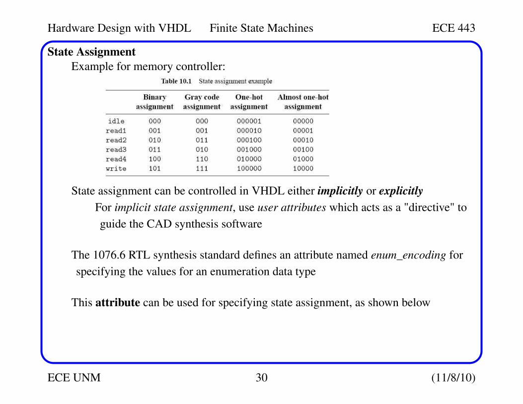
State Assignment
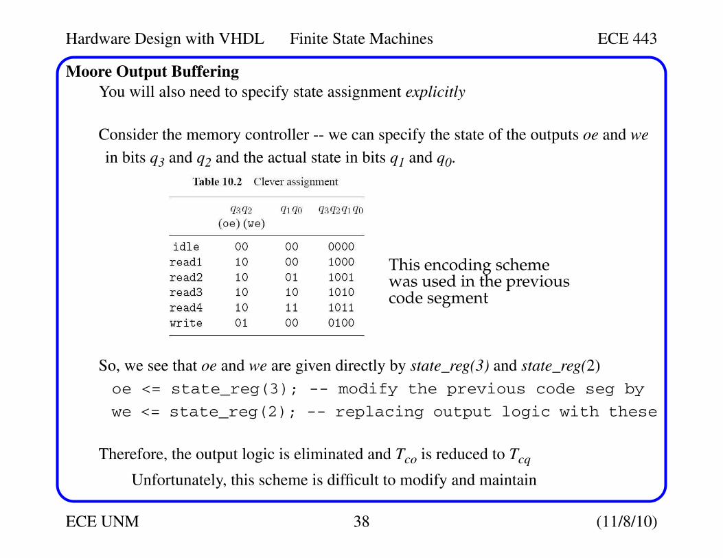
Example for memory controller:
State assignment can be controlled in VHDL either implicitly or explicitly
For implicit state assignment, use user attributes which acts as a "directive" to
guide the CAD synthesis software
The 1076.6 RTL synthesis standard defines an attribute named enum_encoding for
specifying the values for an enumeration data type
This attribute can be used for specifying state assignment, as shown below
Hardware Design with VHDL Finite State Machines ECE 443
ECE UNM 31 (11/8/10)
State Assignment
type mc_state_type is (idle, write, read1, read2,
read3, read4);
attribute enum_encoding: string;
attribute enum_encoding of mc_state_type:
type is "0000 0100 1000 1001 1010 1011";
This user attribute is very common is should be accepted by most synthesis software
Explicit state assignment is accomplished by replacing the symbolic values with