33
Claudio Talarico, Gonzaga University Spring 2015 First and Second Order Circuits

Claudio Talarico, Gonzaga University Spring 2015
First and Second Order Circuits
EE406 – Introduction to IC Design 2
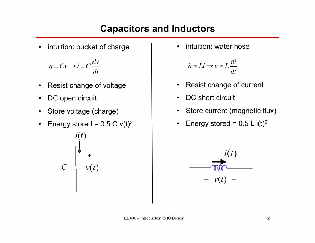
Capacitors and Inductors
• intuition: bucket of charge
• Resist change of voltage
• DC open circuit
• Store voltage (charge)
• Energy stored = 0.5 C v(t)2
q =Cv→ i =C dvdt
C
+"
–")(tv
i(t)
• intuition: water hose
• Resist change of current
• DC short circuit
• Store current (magnetic flux)
• Energy stored = 0.5 L i(t)2
λ = Li→ v = L didt
)(ti
+ v(t) −
EE406 – Introduction to IC Design 3
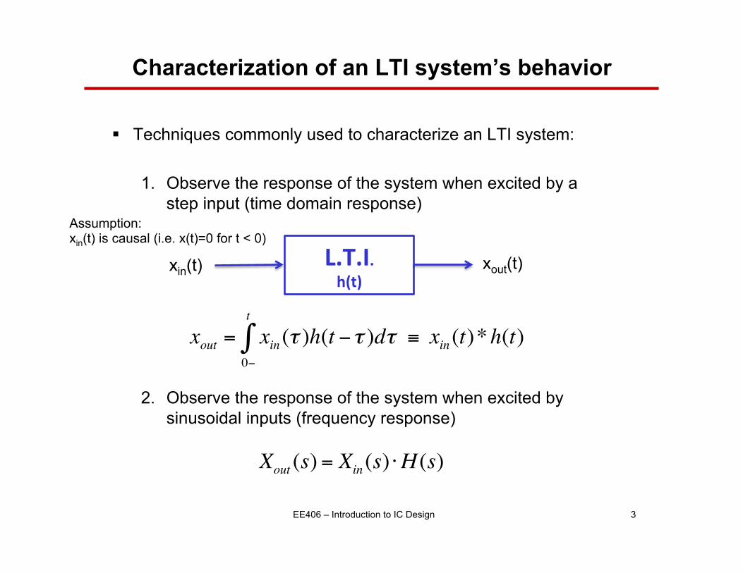
Characterization of an LTI system’s behavior
§ Techniques commonly used to characterize an LTI system:
1. Observe the response of the system when excited by a step input (time domain response)
2. Observe the response of the system when excited by sinusoidal inputs (frequency response)
L.T.I. h(t)
xin(t) xout(t)
xout = xin0−
t
∫ (τ )h(t −τ )dτ ≡ xin (t)*h(t)
Xout (s) = Xin (s) ⋅H (s)
Assumption: xin(t) is causal (i.e. x(t)=0 for t < 0)
EE406 – Introduction to IC Design 4
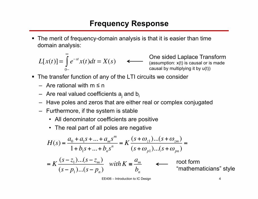
Frequency Response
§ The merit of frequency-domain analysis is that it is easier than time domain analysis:
§ The transfer function of any of the LTI circuits we consider – Are rational with m ≤ n – Are real valued coefficients aj and bi
– Have poles and zeros that are either real or complex conjugated – Furthermore, if the system is stable
• All denominator coefficients are positive • The real part of all poles are negative
L[x(t)]= e− st0−
∞
∫ x(t)dt = X(s) One sided Laplace Transform (assumption: x(t) is causal or is made causal by multiplying it by u(t))
H (s) = a0 + a1s+...+ amsm
1+ b1s+...+ bnsn = K (s+ωz1)...(s+ωzm )
(s+ω p1)...(s+ω pn )=
= K (s− z1)...(s− zm )(s− p1)...(s− pn )
withK ≡ambn
root form “mathematicians” style
EE406 – Introduction to IC Design 5
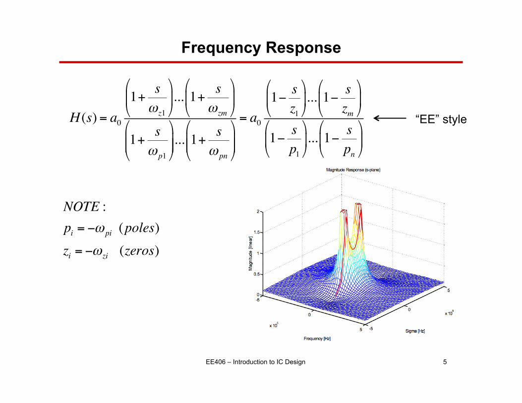
Frequency Response
H (s) = a0
1+ sωz1
!
"#
$
%&... 1+ s
ωzm
!
"#
$
%&
1+ sω p1
!
"##
$
%&&... 1+
sω pn
!
"##
$
%&&
= a0
1− sz1
!
"#
$
%&... 1−
szm
!
"#
$
%&
1− sp1
!
"#
$
%&... 1−
spn
!
"#
$
%&
“EE” style
NOTE :pi = −ω pi (poles)zi = −ωzi (zeros)

EE406 – Introduction to IC Design 6
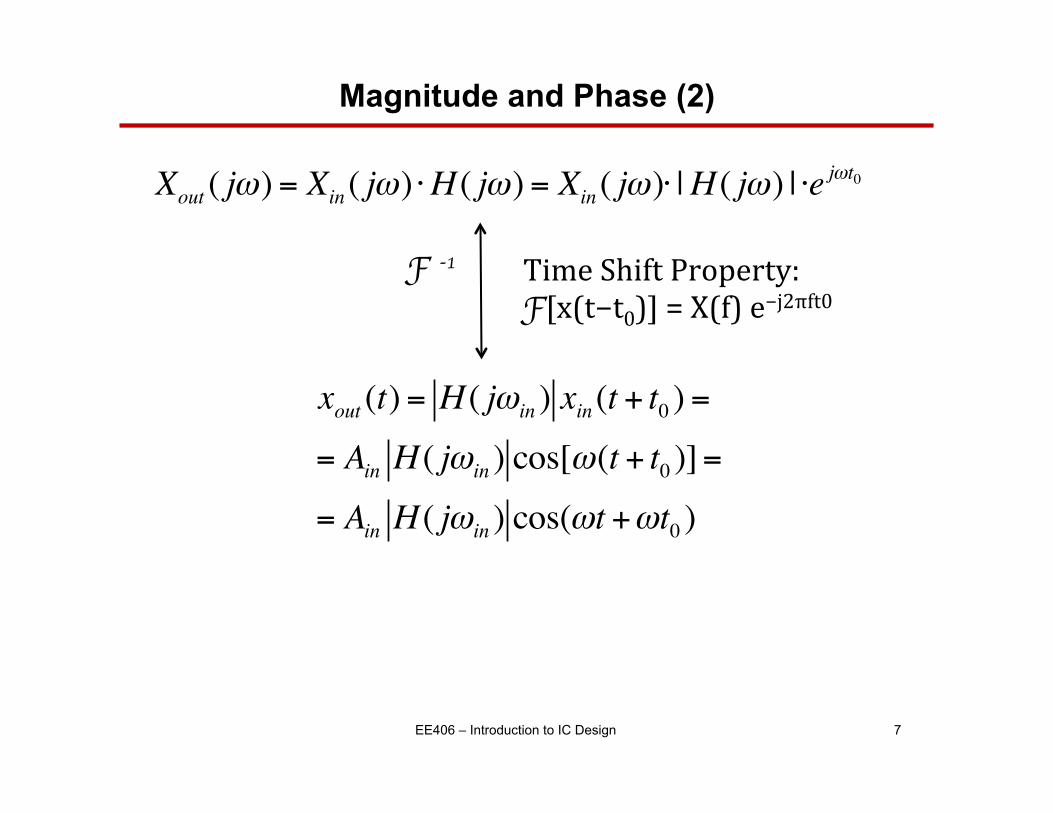
Magnitude and Phase (1)
§ When an LTI system is exited with a sinusoid the output is a sinusoid of the same frequency. The magnitude of the output is equal to the input magnitude multiplied by the magnitude response (|H(jωin)|). The phase difference between the output and input sinusoid is equal to the phase response (ϕ=phase[H(jωin)])
xin (t) = Ain cos(ωt) = Aine jω t + e− jω t
2
RE axis
IM axis
unit circle
1ejθ = cosθ +jsinθ θ
Xin ( jω) = F[xin (t)]
H ( jω) = H ( jω) e jωt0cosθ = e
jθ + e− jθ
2Euler’s formula
F
Xout ( jω) = Xin ( jω) ⋅H ( jω)
EE406 – Introduction to IC Design 7
Magnitude and Phase (2)
xout (t) = H ( jωin ) xin (t + t0 ) =
= Ain H ( jωin ) cos[ω(t + t0 )]=
= Ain H ( jωin ) cos(ωt +ωt0 )
Xout ( jω) = Xin ( jω) ⋅H ( jω) = Xin ( jω)⋅ |H ( jω) | ⋅ejωt0
F -1 Time Shift Property: F[x(t−t0)] = X(f) e−j2πft0

EE406 – Introduction to IC Design 8
First order circuits
§ A first order transfer function has a first order denominator
H (s) = A01+ s
ω p
H (s) = A01+ s
ωz
1+ sω p
First order low pass transfer function. This is the most commonly encountered transfer function in electronic circuits
General first order transfer function.

EE406 – Introduction to IC Design 9
Step Response of first order circuits (1)
§ Case 1: First order low pass transfer function
xin (t) = Ain ⋅u(t) ↔ Xin (s) =Ains
Xout (s) =Ains
A01+ s
ω p
= AinA01s−
1s+ω p
"
#$$
%
&''
!
xout (t) = AinA0u(t) 1− e−t/τ"# %& with τ =1/ω p
H (s) = A01+ s
ω p

EE406 – Introduction to IC Design 10
Step Response of first order circuits (2)
§ Case 2: General first order transfer function
xin (t) = Ain ⋅u(t) ↔ Xin (s) =Ains
Xout (s) =AinA0s
1+ sωz
1+ sω p
!
xout (t) = AinA0u(t) 1− 1−ω p
ωz
"
#$
%
&'e−t/τ
(
)**
+
,--
where τ =1/ω p
H (s) = A01+ s
ωz
1+ sω p

EE406 – Introduction to IC Design 11
Step Response of first order circuits (3)
§ Notice xout(t) “short term” and “long term” behavior
§ The short term and long term behavior can also be verified using the Laplace transform
xout (0+) = AinA0ω p
ωz
xout (∞) = AinA0
xout (0+) = lims→∞ s ⋅Xout (s) = lims→∞ sAins⋅H (s) = AinA0
ω p
ωz
xout (∞) = lims→0 s ⋅Xout (s) = lims→0 sAins⋅H (s) = AinA0
EE406 – Introduction to IC Design 12
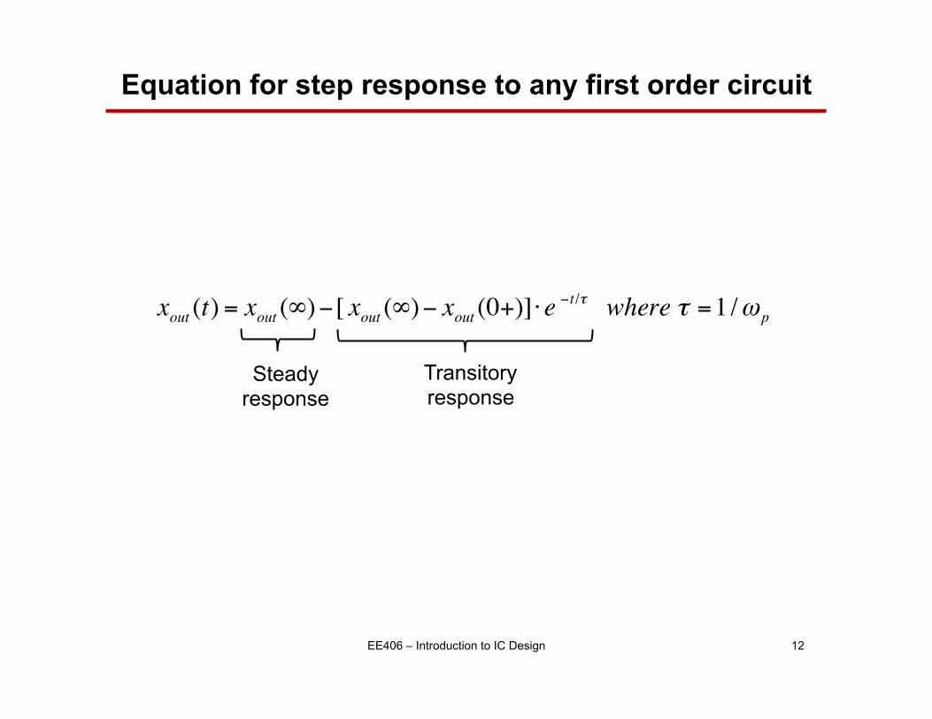
Equation for step response to any first order circuit
xout (t) = xout (∞)−[ xout (∞)− xout (0+)]⋅e−t/τ where τ =1/ω p
Steady response
Transitory response
EE406 – Introduction to IC Design 13
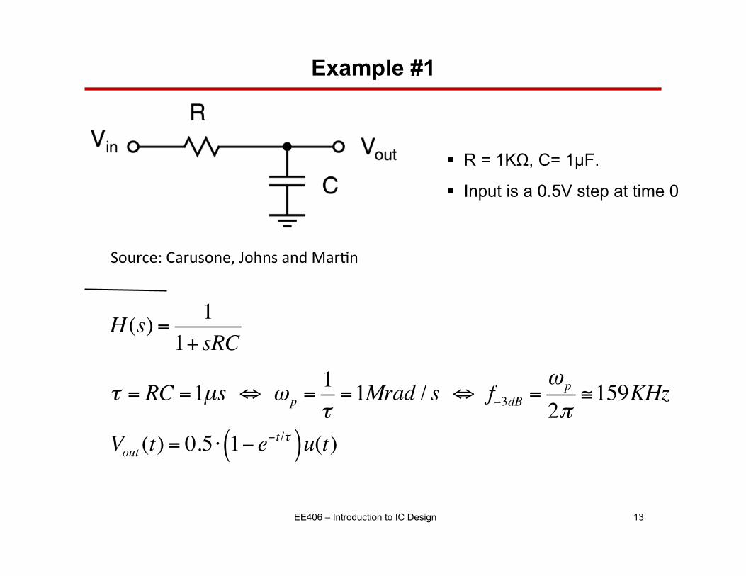
Example #1
§ R = 1KΩ, C= 1µF.
§ Input is a 0.5V step at time 0
Source: Carusone, Johns and Mar2n
H (s) = 11+ sRC
τ = RC =1µs ⇔ ω p =1τ=1Mrad / s ⇔ f−3dB =
ω p
2π≅159KHz
Vout (t) = 0.5 ⋅ 1− e−t/τ( )u(t)

EE406 – Introduction to IC Design 14
Example #2 (1)
Source: Carusone, Johns and Mar2n
§ R1 = 2KΩ, R2=10KΩ
§ C1= 5pF. C2=10pF
§ Input is a 2V step at time 0
H (s) = R2R1 + R2
⋅1+ sR1C1
1+ s R1R2R1 + R2
(C1 +C2 )
"
#
$$$$
%
&
''''
By inspection
H (s→ 0) = R2R1 + R2
≡ A0; H (s→∞) = C1C1 +C2
≡ A∞
τ p = (R1 || R2 ) ⋅ (C1 ||C2 ) =R1R2R1 + R2
(C1 +C2 )
τ z = R1C1

EE406 – Introduction to IC Design 15
Example #2 (2)
= AinR2
R1 + R2
AinC1
C1 +C2=
Vout(t)
Vout(0+)
Vout(∞)
Vout (0+)+ Vout (∞)−Vout (0+) ⋅ 1− e−t/τ p( )$
%&' for t > 0
Vout (t) =0 for t ≤ 0

EE406 – Introduction to IC Design 16
Example #3
§ Consider an amplifier having a small signal transfer function approximately given by
§ Find approx. unity gain BW and phase shift at the unity gain frequency
since A0 >> 1:
A(s) = A01+ s
ω p
§ A0 = 1 x 10⁵
§ ωp = 1 x 10³ rad/s
A(s) ≈ A0sω p
=A0ω p
s
A0ω p
jωu
=1 ⇒ ωu ≅ A0ω p
A( jω) ≈A0ω p
jω
Phase[A( jωu )] ≈ PhaseA0ω p
jωu
"
#$
%
&'= −90!

EE406 – Introduction to IC Design 17
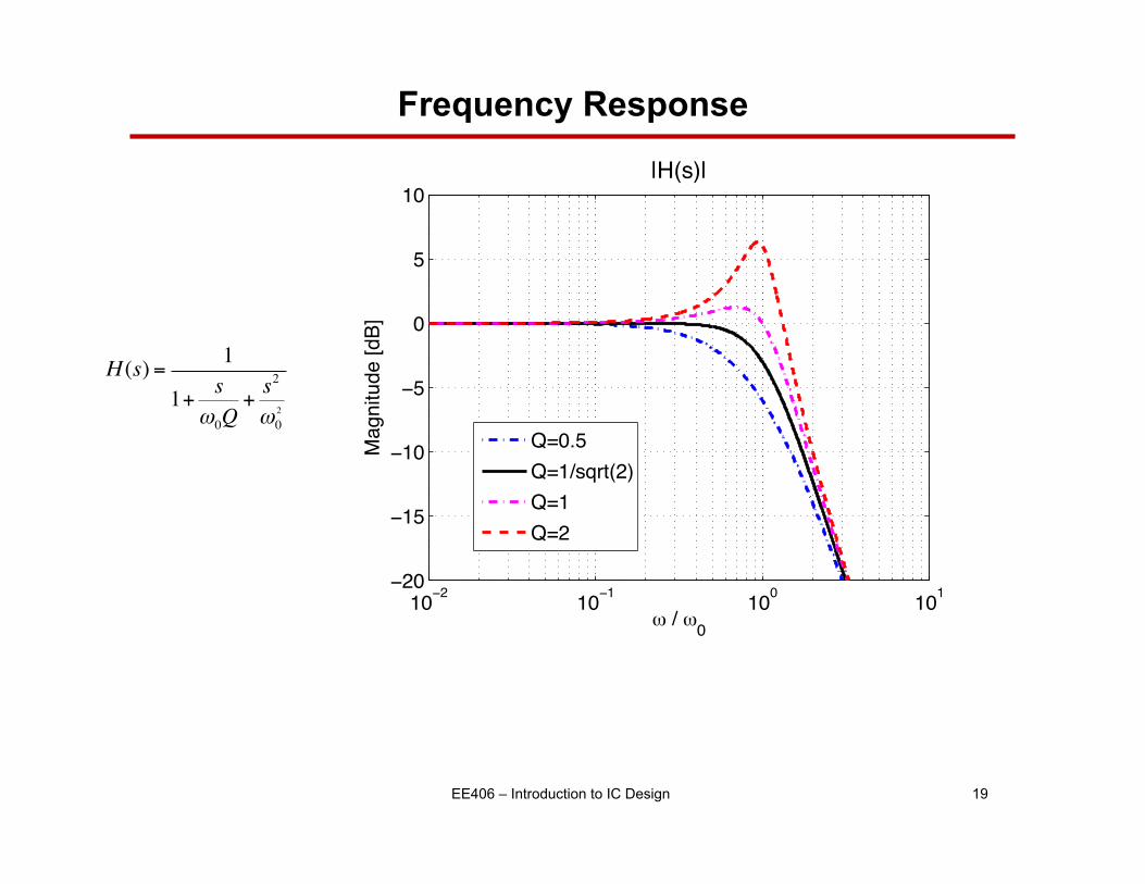
Second-order low pass Transfer Function
§ Interesting cases: - Poles are real
- one of the poles is dominant - Poles are complex
ω3dB ≅1b1 b1 = τ j∑( )
H (s) = a01+ b1s+ b2s
2=
a0
1+ sω0Q
+s2
ω02
b1 ≡1
ω0Q; b2 ≡
1ω02

EE406 – Introduction to IC Design 18
Poles Location
1+ sω0Q
+s2
ω02= 0§ Roots of the denominator of the transfer function:
§ Complex Conjugate poles (overshooting in step response)
- For Q = 0.707 (Φ=45°), the -3dB frequency is ω0 (Maximally Flat Magnitude or Butterworth Response)
- For Q > 0.707 the frequency response has peaking
§ Real poles (no overshoot in the step response)
for Q > 0.5 ⇒ p1,2 = −ω0
2Q 1∓ j 4Q2 −1( ) = −ωR ∓ jω I
for Q ≤ 0.5 ⇒ p1,2 = −ω0
2Q 1∓ 1− 4Q2( )
Poles location with Q> 0.5
jω
σ Φ =
Source: Carusone
EE406 – Introduction to IC Design 19
Frequency Response
10−2 10−1 100 101−20
−15
−10
−5
0
5
10
t / t0
Mag
nitu
de [d
B]
|H(s)|
Q=0.5Q=1/sqrt(2)Q=1Q=2
H (s) = 1
1+ sω0Q
+s2
ω02
EE406 – Introduction to IC Design 20
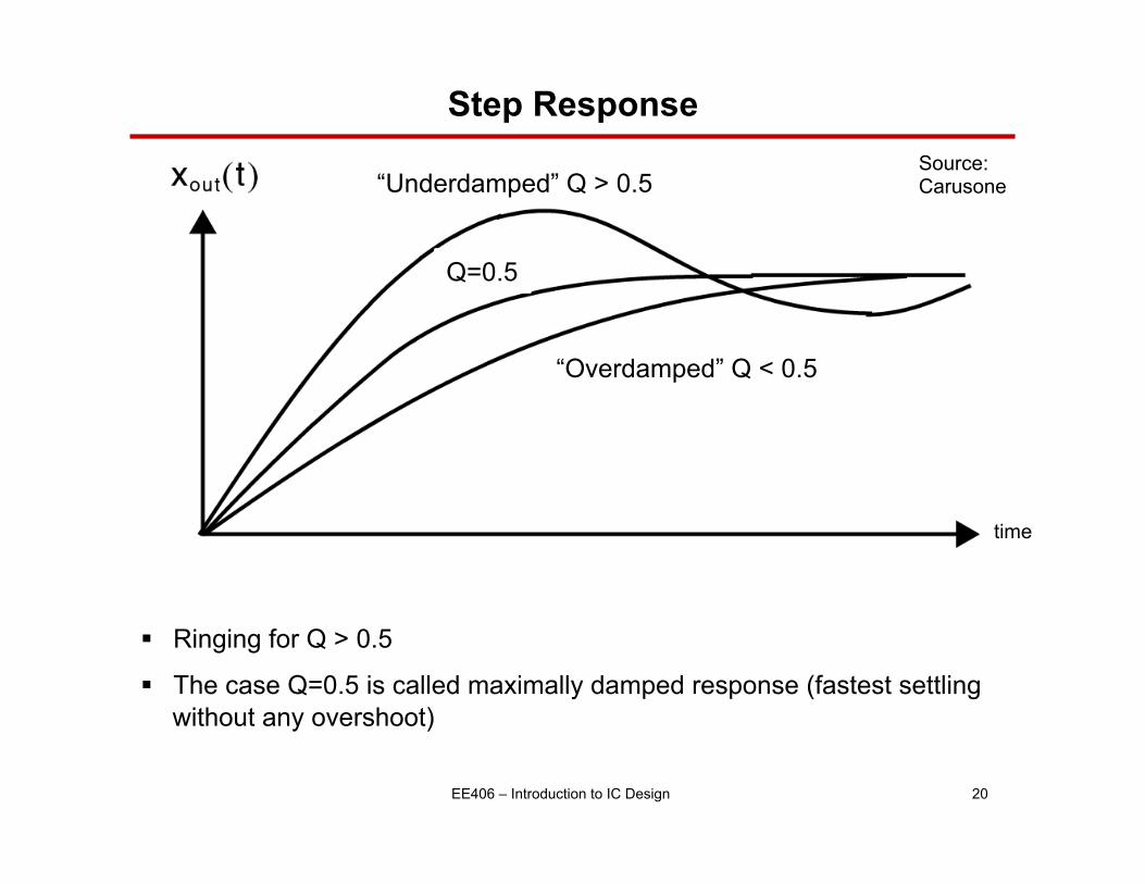
Step Response
§ Ringing for Q > 0.5
§ The case Q=0.5 is called maximally damped response (fastest settling without any overshoot)
“Underdamped” Q > 0.5
“Overdamped” Q < 0.5
Q=0.5
Source: Carusone
time

EE406 – Introduction to IC Design 21
Widely- Spaced Real Poles
Real poles occurs when Q ≤ 0.5:
Real poles widely-spaced (that is one of the poles is dominant) implies:
for Q ≤ 0.5 ⇒ p1,2 = −ω0
2Q 1∓ 1− 4Q2( )
H (s) = a01+ b1s+ b2s
2=
a0
1+ sω0Q
+s2
ω02
b1 ≡1
ω0Q; b2 ≡
1ω02
p1 ≡ −ω0
2Q −ω0
2Q1− 4Q2 << p2 ≡ −
ω0
2Q +ω0
2Q1− 4Q2
!
0 << 2 1− 4Q2 ⇔ 0 << 1− 4Q2 ⇔ 0 <<1− 4Q2 ⇔Q2 <<14⇔
b2b12 <<
14

EE406 – Introduction to IC Design 22
Widely-Spaced Real Poles
This means that in order to estimate the -3dB bandwidth of the circuit, all we need to know is b1 !
ZVTC method:
H (s) = a01+ b1s+ b2s
2 =a0
1− sp1
"
#$
%
&'⋅ 1−
sp2
"
#$
%
&'
=a0
1− sp1−sp2+
s2
p1p2
≅a0
1− sp1+
s2
p1p2
⇒ p1 ≅ −1b1
p2 ≅1p1b2
= −b1
b2
H (s) ≅ a0
1− sp1
⇒ω-3dB ≅ p1 ≅1b1
b1 = τ j∑ ⇒ω−3dB ≅1b1
=1τ j∑
EE406 – Introduction to IC Design 23
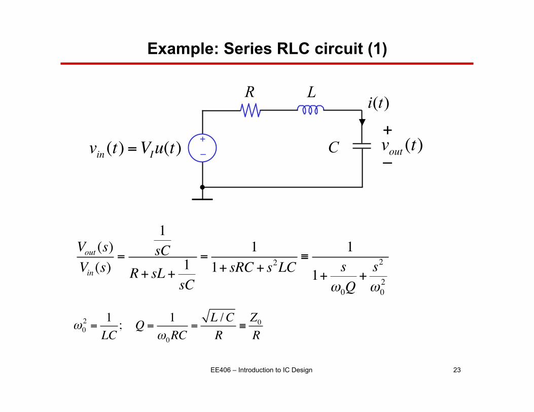
Example: Series RLC circuit (1)
vin (t) =VIu(t)+"–" C
R L
+"
–"vout (t)
)(ti
Vout (s)Vin (s)
=
1sC
R+ sL + 1sC
=1
1+ sRC + s2LC≡
1
1+ sω0Q
+s2
ω02
ω02 =
1LC; Q =
1ω0RC
=L /CR
≡Z0R
EE406 – Introduction to IC Design 24
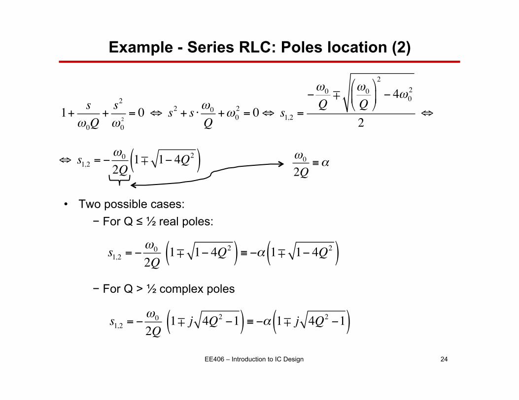
• Two possible cases: − For Q ≤ ½ real poles: − For Q > ½ complex poles
1+ sω0Q
+s2
ω02= 0 ⇔ s2 + s ⋅ω0
Q+ω0
2 = 0⇔ s1,2 =−ω0
Q∓ ω0
Q$
%&
'
()
2
− 4ω02
2⇔
⇔ s1,2 = −ω0
2Q1∓ 1− 4Q2( )
s1,2 = −ω0
2Q 1∓ j 4Q2 −1( ) ≡ −α 1∓ j 4Q2 −1( )
s1,2 = −ω0
2Q 1∓ 1− 4Q2( ) ≡ −α 1∓ 1− 4Q2( )
Example - Series RLC: Poles location (2)
ω0
2Q≡α

EE406 – Introduction to IC Design 25
Example – series RLC
Vout (s)Vin (s)
=
1sC
R+ sL + 1sC
=1
1+ sRC + s2LC≡
1
1+ s Qω0
+s2
ω02
ω02 =
1LC; Q =
1ω0RC
=L /CR
≡Z0R; ω0
2Q≡α
C = 1L ⋅ω0
2 ; L =1
C ⋅ω02
Q =1
RCω0
=LR⋅1ω0
α =ω0
2Q=R2L
EE406 – Introduction to IC Design 26
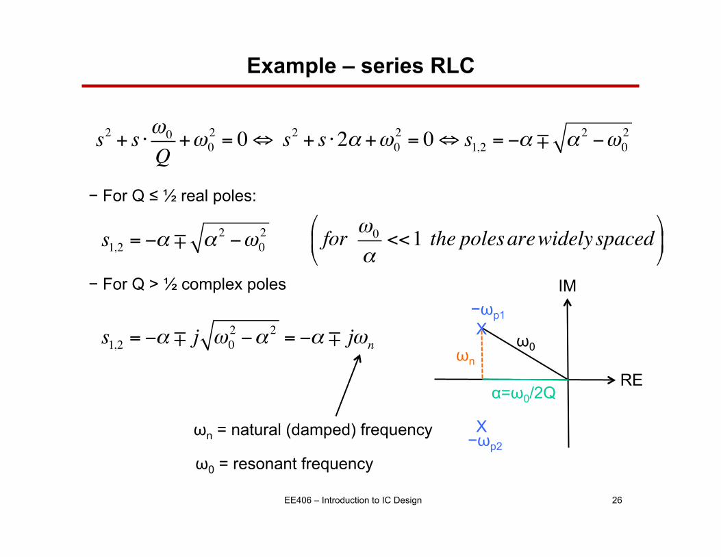
Example – series RLC
− For Q ≤ ½ real poles:
− For Q > ½ complex poles
s2 + s ⋅ω0
Q+ω0
2 = 0⇔ s2 + s ⋅2α +ω02 = 0⇔ s1,2 = −α ∓ α 2 −ω0
2
s1,2 = −α ∓ α 2 −ω02 for ω0
α<<1 the polesarewidely spaced
!
"#
$
%&
s1,2 = −α ∓ j ω02 −α 2 = −α ∓ jωn
X X
ωn
α=ω0/2Q
ω0
−ωp1
RE
IM
ωn = natural (damped) frequency −ωp2
ω0 = resonant frequency

EE406 – Introduction to IC Design 27
Example – series RLC: Step response
(a) Overdamped Q < 0.5 (α > ω0 )
(b) Critically damped Q=0.5 (α = ω0 )
(c) Underdamped Q > 0.5 (α < ω0 )
vout(t)
time
⇔ζ ≡α /ω0 >1
⇔ζ ≡α /ω0 =1⇔ζ ≡α /ω0 <1
α = damping factor (rate of decay) ω0 = resonance frequency ζ = Damping ratio
ωn = ringing frequency
EE406 – Introduction to IC Design 28
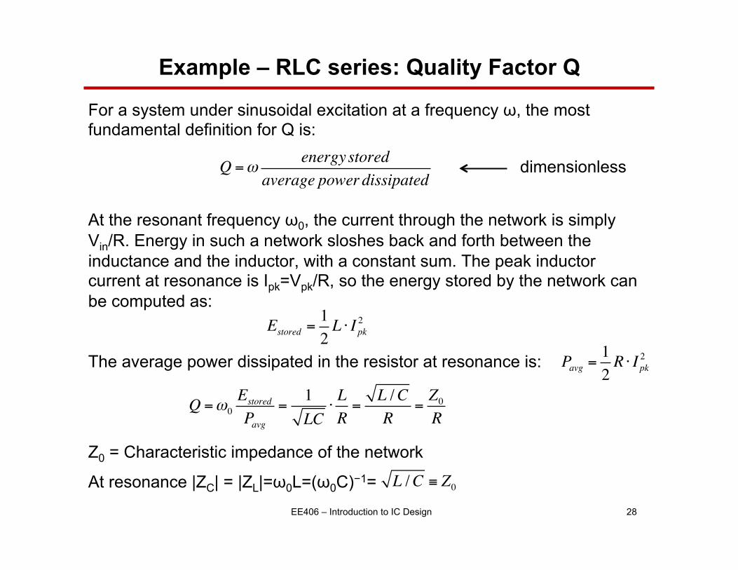
Example – RLC series: Quality Factor Q
For a system under sinusoidal excitation at a frequency ω, the most fundamental definition for Q is:
At the resonant frequency ω0, the current through the network is simply Vin/R. Energy in such a network sloshes back and forth between the inductance and the inductor, with a constant sum. The peak inductor current at resonance is Ipk=Vpk/R, so the energy stored by the network can be computed as:
The average power dissipated in the resistor at resonance is:
Z0 = Characteristic impedance of the network
At resonance |ZC| = |ZL|=ω0L=(ω0C)−1=
Q =ωenergystored
average power dissipated
Estored =12L ⋅ I pk
2
Pavg =12R ⋅ I pk
2
Q =ω0Estored
Pavg=
1LC
⋅LR=
L /CR
=Z0R
dimensionless
L /C ≡ Z0
EE406 – Introduction to IC Design 29
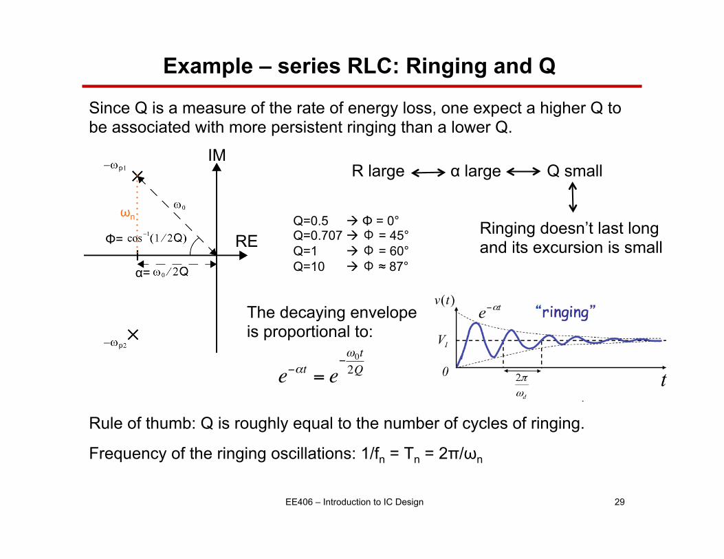
Example – series RLC: Ringing and Q
Since Q is a measure of the rate of energy loss, one expect a higher Q to be associated with more persistent ringing than a lower Q.
Rule of thumb: Q is roughly equal to the number of cycles of ringing.
Frequency of the ringing oscillations: 1/fn = Tn = 2π/ωn
IM
RE
R large α large Q small
The decaying envelope is proportional to:
Ringing doesn’t last long and its excursion is small
ωn
α=
e−αt = e−ω0t2Q
Φ= Q=0.5 à Φ = 0° Q=0.707 à Φ = 45° Q=1 à Φ = 60° Q=10 à Φ ≈ 87°
EE406 – Introduction to IC Design 30
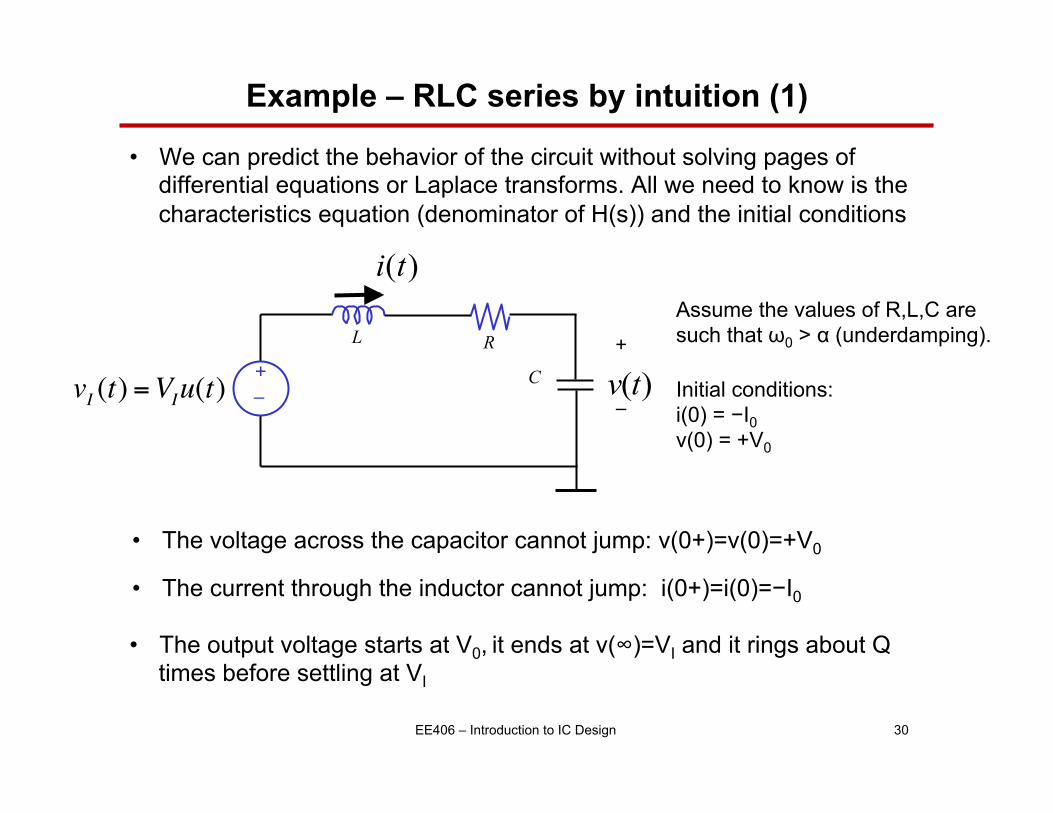
Example – RLC series by intuition (1)
• We can predict the behavior of the circuit without solving pages of differential equations or Laplace transforms. All we need to know is the characteristics equation (denominator of H(s)) and the initial conditions
• The output voltage starts at V0, it ends at v(∞)=VI and it rings about Q times before settling at VI
Assume the values of R,L,C are such that ω0 > α (underdamping). Initial conditions: i(0) = −I0 v(0) = +V0
+"–"
C
L +"
–")(tvvI (t) =VIu(t)
)(ti
R
• The voltage across the capacitor cannot jump: v(0+)=v(0)=+V0 • The current through the inductor cannot jump: i(0+)=i(0)=−I0
EE406 – Introduction to IC Design 31
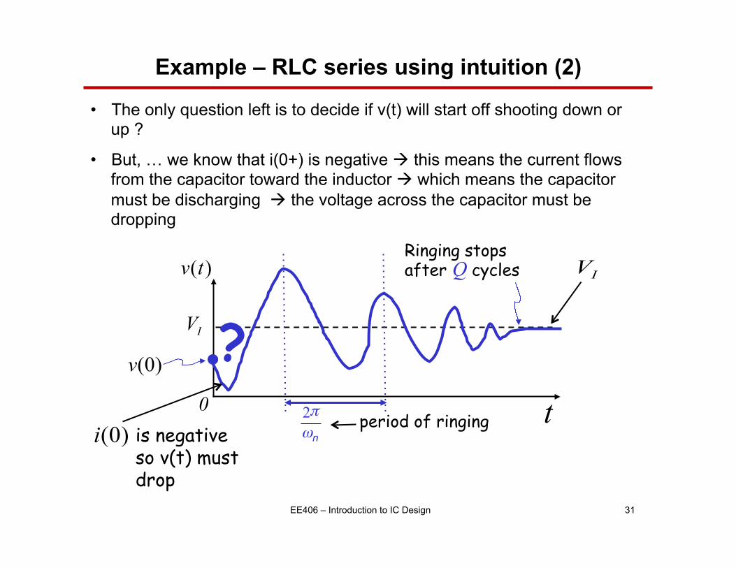
Example – RLC series using intuition (2)
• The only question left is to decide if v(t) will start off shooting down or up ?
• But, … we know that i(0+) is negative à this means the current flows from the capacitor toward the inductor à which means the capacitor must be discharging à the voltage across the capacitor must be dropping
)(tv
t
IV
0
IV
ωn
π!2! period of ringing
Q !
Ringing stops after cycles
)0(v ?)0(i is negative
so v(t) must drop

EE406 – Introduction to IC Design 32
Example – RLC series using intuition (3)
• In practice for the under damped case it useful to compute two parameters
• Overshoot • Settling time
OS = exp −πωn
α"
#$
%
&' Normalized overshoot =
% overshoot w.r.t. final value
ts ≅ −1αln ε
ωn
ω0
#
$%
&
'( ε is the % error that we are willing
to tolerate w.r.t. the ideal final value
EE406 – Introduction to IC Design 33
First order vs. Second order circuits Behavior
• First order circuits introduce exponential behavior
• Second order circuits introduce sinusoidal and exponential behavior combined
• Fortunately we will not need to go on analyzing 3rd, 4th, 5th and so on circuits because they are not going to introduce fundamentally new behavior


