e. Strong coupling regime. e. Molecule. First Lecture. Chemical structure. Functions: macroscopic electronic properties . Molecular Wires. Diodes. Negative Differential Resistance (NDR) elements. Switches and storage elements. - PowerPoint PPT Presentation
66
M. F. Goffman First Lecture Functions: macroscopic electronic properties Molecular Wires Diodes Switches and storage elements Negative Differential Resistance (NDR) elements Chemical structure • Transport mechanisms are determined by Metal-molecule coupling Weak coupling regime e e Molecule Strong coupling regime Molecule
Transcript
M. F. Goffman
First Lecture
• Functions: macroscopic electronic properties
Molecular Wires
Diodes
Switches and storage elements
Negative Differential Resistance (NDR) elements
Chemical structure
• Transport mechanisms are determined by Metal-molecule coupling
Weak coupling regime
ee
Molecule
Strong coupling regime
Molecule
M. F. Goffman
Second Lecture
• Functions: macroscopic electronic properties
Molecular Wires
Diodes
Switches and storage elements
Negative Differential Resistance (NDR) elements
Chemical structure
• Transport mechanisms are determined by Metal-molecule coupling
Weak coupling regime
ee
Molecule
Strong coupling regime
Molecule
1
2
Qualitative Picture
3 Final Remarks
M. F. Goffman
Molecular Conduction: Qualitative Picture
Energy Diagram showing the molecular levels relative to the electrochemical potential of electrodes
Potential Profile across the molecule due to the applied bias.
Two Basic Ingredients:
M. F. Goffman
M0
Strong Coupling to Metallic Electrodes ()
Isolated Molecule
E
HOMO
LUMO
Discrete Energy Levels Broadening of the energy levels ()
M0 Mn Fractional charge transfer
Which is the location µF with respect to HOMO-LUMO levels?
E
Local Density of States
Fermi level µF
Mn
Chemically bonded
M. F. Goffman
Location of the Fermi Energy
UPS Experiments (UV Photo Electron Spectroscopy )
h e-
S S e h
E
Local Density of States
Mn
h
e-
e-
µF
h
EµF# e
per
seco
nd
EµF
HOMO
Vacuum Level
Vacuum Level
e-
EH
OM
O
UPS spectrum
# e
per
seco
nd
M. F. Goffman
1.5 1.0 0.5 0.0 -0.50.0
0.2
0.4
0.6
0.8
1.0
1.2
Inte
nsity
(10
4 coun
ts p
er s
econ
d)
Binding energy-µF (eV)
UPS Experiment on Self-assembled Monolayer on Au
SeCOCH3CH3COSeS
S
S
Se3
h e-
he-
HOMO FE E µ
M. F. Goffman
Energy Diagram
µ L=µR
-V/2 V/2L R L R
µ L
µR
eV
At equilibrium (V=0)
But how are µL and µR disposed with respect to the molecular levels?
Potential profile inside the molecule
M. F. Goffman
Potential Profile
To the lowest approximation Molecular Levels shift "rigidly" by
(r) / 2V V with 0 1 molV
e (r)molV
Let us denote this average potential as:
Taking the molecular levels as our reference, the electrochemical potential of electrodes are shifted by
L F Vµ µ e R F eVµ µ 1
This voltage division factor has a profound effect on Current-Voltage Characteristics
-V/2 V/2L R
Potential Profile
-V/2
V/2
(r)molVrV
M. F. Goffman
Energy Level Diagram (=0)
=0 Molecular levels remain fixed to µ L
V>0 HOMO Conduction V<0 LUMO Conduction
I-V Characteristics can look asymetric Positive branch (V>0) and Negative branch (V<0) involve different Molecular levels
µ L
µR
eV
LUMO
HOMO
µ L
µR
eV
LUMO
HOMO
M. F. Goffman
Energy Level Diagram (=1/2)
=1/2 Molecular levels shift with respect to µ L by half the applied bias
µ L
µR
eV/2
LUMO
HOMO
µ L µR
eV/2
LUMO
HOMO
Conduction takes place through the nearest molecular level (HOMO in this case) for either bias polarity.
M. F. Goffman
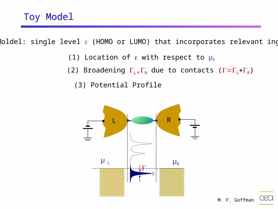
Toy Model
(1) Location of with respect to µF
(2) Broadening L,R due to contacts (LR)
Toy Moldel: single level (HOMO or LUMO) that incorporates relevant ingredients:
(3) Potential Profile
L R
µ L µR
M. F. Goffman
Discrete One-Level Model
-V/2 V/2L R
µ L
LR
L
-0.2
-0.1
0.0
0.1
0.2
0.0 0.5 1.0
f
E-µ
F (
eV)
µR
R
0.0 0.5 1.0-0.2
-0.1
0.0
0.1
0.2
E-µ
F (
eV)
f
B/ k T
1f Fermi function
1 e
Current as a "balancing act" L Rf µ N f µ
M. F. Goffman
Discrete One-Level Model
-V/2 V/2L R
µ L
LR
-0.2
-0.1
0.0
0.1
0.2
0.0 0.5 1.0
f
E-µ
F (
eV)
L L
available state
L
s
Outflow N 1 f µ
L L
available states
LInflow f µ 1 N
L L L LLI e Inflow Outflow e N f µ
The net flux across left junction will be
L
M. F. Goffman
Discrete One-Level Model
-V/2 V/2L R
LR
The net flux across right junction will be
RR RI e N f µ
µR
R
0.0 0.5 1.0-0.2
-0.1
0.0
0.1
0.2
E-µ
F (
eV)
f
M. F. Goffman
Discrete One-Level Model
At the steady state IL+IR=0 (no charge accumulation in the molecule)
L RL
R
R
L
f µ f µN
L RL
RL R
RL
eI I f µ f µI
R LR L R RI I e N f µ e N f µ 0
The current through the metal-molecule-metal structure will be
M. F. Goffman
-1.2 -0.8 -0.4 0.0 0.4 0.8 1.2-40
-30
-20
-10
0
10
20
30
40
I (µ
A)
V (Volts)
µ L µR
µ L
µR
µ L
µR
One-level Model: Current (I) vs. Voltage (V)
L
R
L R
F
F
F
V
V
µ µ e / 2
µ µ e / 2
µ 0.4eV
0.1eV 0.2eV
L R
L RL RI
ef µ f µ
Let us take into account Broadening of the level
F2 µ
M. F. Goffman
Broadening
We replace the discrete level by a Lorentzian density of states:
µ L
µR
L
R
2 2
1D E
2 E / 2
L
LL
R
RR
eD E f E µ fI E µ dE
Expression of the current will be modified
We could write in the Landauer-Büttiker form
L RL R
L R
eT E f E µ f E µ dE where T E 2I D E
2
I let for you the demostration that the maximum value of 2
V2
Ie
G /
M. F. Goffman
-1.2 -0.8 -0.4 0.0 0.4 0.8 1.2-20
0
20
40
60
80
100
120
140
G (
µS)
V (Volts)
One-level Model: Current (I) vs. Voltage (V)
Next: Potential Profile
L
R
L R
F
F
F
V
V
µ µ e / 2
µ µ e / 2
µ 0.4eV
0.2eV 0.1eV
-1.2 -0.8 -0.4 0.0 0.4 0.8 1.2-40
-30
-20
-10
0
10
20
30
40
Broadened Discrete
I
(µA)
V (Volts)
Conductance Quantum
M. F. Goffman
Potential Profile
The potential profile VMOL(r) will be obtained by solving
r 0r e n/ Poisson's Equation
MOLV
A solution can be visualized in terms of a capacitance circuit model:
-V/2 V/2L R -V/2 V/2
CL CR
L Re n C / 2 CV V/ 2
2R Le C C
U e n eVC C
Charging Energy Eadd rSolution of r 0
MOLV
Fn N f µ : change in the number of electrons @ equilibrium
The potential U that raises the position of the level is
r MOLV
M. F. Goffman
Self Consistent Solution
Fadd0 0 0
U(N)
N VE f µ D E D E U N
L
L R
RRLf E µ f E µN D E U N dE
Iterative Procedure for calculating N and U self-consistently
L R
LL R
R
eD E U N f µ f dI E E µ E
M. F. Goffman
µ L
µR
V>0
One-level Model: Current (I) vs. Voltage (V)
-1.2 -0.8 -0.4 0.0 0.4 0.8 1.20
20
40
G (
µS)
V (Volts)
IV asymetric
Coupling asymetry + charging
-1.2 -0.8 -0.4 0.0 0.4 0.8 1.2-30
-20
-10
0
10
20
30
Eadd
=0.0 eV E
add=0.3 eV
I
(µA)
V (Volts)
µ L
µR
V<0
Positively charges the molecule
shift down
L R0.2eV 0.1eV
M. F. Goffman
Summary
addWhen transport can be described using a "self-consistent field" meE thod
Asymetric IVs asymetric coupling + charging effect (Eadd) even if transport is associated with a single level (symetric molecule)
HOMO conduction I is lower for positive bias on the stronger contact
LUMO conduction I is higher for positive bias on the stronger contact
-1.2 -0.8 -0.4 0.0 0.4 0.8 1.2-30
-20
-10
0
10
20
30
Eadd
=0.0 eV E
add=0.3 eV
I (µ
A)
V (Volts)
• I increases when is crossed at V~2(µF-)
• I increases over a voltage width +kBT
• I dragged out by charging Eadd
M. F. Goffman
Realistic Models
Non-Equilibrium Green's Function (NEGF) Formalism
Let us rewritte the previous eq. in terms of a Green Function G(E)
1G E
E i / 2
Then the density of states will be proportional to the so called Spectral function defined as
† A EA E i G E G E D E
2
The mean number of excess electrons N and the current can be written as
2 2
1 2
1
1 2
2
12 2
2N dE G E f E µ G E f E µ
2
2eI dE G E f E µ f E µ
M. F. Goffman
NEGF Formalism
For a multilevel Molecule (n levels) all quantities are replaced by a corresponding matrix (n x n )
Hamiltonian Matrix
Broadenning Matrix
D E A E / 2 Spectral Function
N Density Matrix
U U Self consistent
Potential
H
1G E
E i / 2
†1G E i
E S H
A pedagogical tutorial: S. Datta, Nanotechnology 15, S433 (2004).
H : Molecule + surface atoms
: Coupling to bulk contacts
U : appropriate functional
M. F. Goffman
Experiments on Molecular Wires
Well coupled to electrodes (at least one of them)
M. F. Goffman
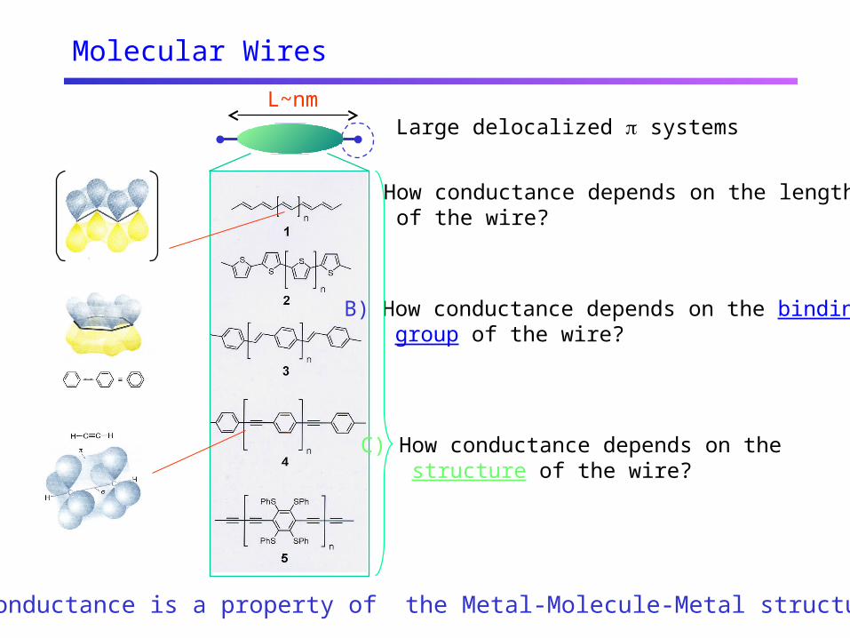
Molecular Wires
A) How conductance depends on the length L of the wire?
L~nmLarge delocalized systems
Conductance is a property of the Metal-Molecule-Metal structure
B) How conductance depends on the binding group of the wire?
C) How conductance depends on the structure of the wire?
M. F. Goffman
How one can measure transport properties of molecular wires?
1) STM: Scanning Tunneling Microscope
2) Break-junctions
Electronmigration-induced
Mechanically controlled
3) Shadow evaporation on Self-assembled Monolayers (SAMs)
M. F. Goffman
Adsorption
MBE: Molecular "Beaker" Epitaxy
Organization
SolutionThiol-endedMolecules
Au (111)
STM Image
s s s s s s s s sAu (111)
Tip
M. F. Goffman
A) How conductance depends on L?
M. F. Goffman
Conductive AFM on Self-Assembled Monolayers
Sakaguchi et al., APL 2001
=0.41Å-1 for oligothiophene=1.08 Å-1 for alkanethiol
Measured
Theory
=0.33Å-1 for oligothiophene=1.0 Å-1 for alkanethiol
M. F. Goffman
Langlais et al., PRL 1999
t m v
m v
I G ( )exp( ) since
G ( ) exp( ) wi
x x
x
z z
x th
Conductance depends exponentially on L
STM on specially designed molecular wire
M. F. Goffman
Explanation
-V/2V/2
L R
µ L
µR
eV
At low voltages µF is far from HOMO and/or LUMO Tunneling Transmission
M. P. Samanta et al., PRB 53, R7626 (1996).
M. F. Goffman
B) How conductance depends on the binding group of the molecular wire?
M. F. Goffman
Experiments are needed
Conductance of molecular wires: Influence of molecule-electrode binding. S.N. Yaliraki, M.
Kemp, and M.A. Ratner, J. Am. Chem. Soc. 121(14), 3428 (1999)
Se > S
Theoretical studies
Molecular alligator clips for single molecule electronics. Studies of group 16 and isonitriles
interfaced with Au contacts. J.M. Seminario, A.G. Zacarias, and J.M. Tour
J. Am. Chem. Soc. 121(2), 411 (1999)
S > Se
X=S T3
X=Se Se3XCH3COX
S S
S
Influence of the binding group of electroactive molecules
X = S or Se
M. F. Goffman
Influence of the binding group: Se vs S
Investigation of T3 and Se3S
SCOCH3CH3COSS
S
SeCOCH3CH3COSeS
S
S
T3
Se3
T3
Se3
“Identical” HOMOs quite similar IPs
6.50 eV
6.52 eV
M. F. Goffman
Sample Preparation
Adsorption
Organization
Solution
ConductingMolecules
Au (111)
SolutionThiol-endedInsulating Molecules
Insertion
M. F. Goffman
STM tip
28 nm T3,Vt = +0.78V, It = 10.7pA
L. Patrone et al, Chem. Phys.281(2002)325PRL 91(03) 096802
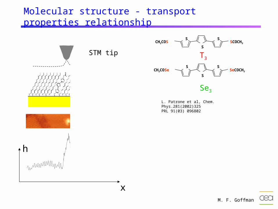
Molecular structure - transport properties relationship
h
x
SSCOCH3CH3COS
S
S
SeCOCH3CH3COSeS
S
S
T3
Se3
M. F. Goffman
STM tip
28 nm T3,Vt = +0.78V, It = 10.7pA
L. Patrone et al, Chem. Phys.281(2002)325PRL 91(03) 096802
Molecular structure - transport properties relationship
h
x
SSCOCH3CH3COS
S
S
SeCOCH3CH3COSeS
S
S
T3
Se3
M. F. Goffman
STM tip
28 nm T3,Vt = +0.78V, It = 10.7pA
L. Patrone et al, Chem. Phys.281(2002)325PRL 91(03) 096802
Molecular structure - transport properties relationship
The apparent height is a (relative) measure of the conductance of the molecular junction
h
x
SSCOCH3CH3COS
S
S
SeCOCH3CH3COSeS
S
S
T3
Se3
M. F. Goffman
S vs Se: Experimental comparison
It It
STM tip
28 nm T3,Vt = +0.78V, It = 10.7pA
L. Patrone et al, Chem. Phys. 281(2002)325
T3
Se3
Topography: 1.0 nm
Topography: 1.0 nm
STM on T3 and Se3 Molecules inserted in a dodecanethiol Matrix
M. F. Goffman
Se give rise to a more efficient transport than S
0 1 2 3 4 5 6 7 8 9 1011
Se3
Vt=+0.78VIt=3.5pA
Nu
mb
er
of
mo
lecu
les
(a.u
.)
Apparent height (Å)
T3
-1 0 10
1
2
3
4
5
6
Ap
pa
ren
t h
eig
ht
(Å)
Tunneling bias (V)
T3 (S)
Se3 (Se)
Se3 > T3
S vs Se: Experimental comparison
M. F. Goffman
Current-Voltage characteristic
IV
eV
I
2(EF-EHOMO)
Se3
T3
EF
HOMOLUMO
Position of the HOMO level/ Fermi level
(EF-EHOMO) : T3 > (EF-EHOMO) : Se3
EF-EHOMO
eV
M. F. Goffman
UPS (UV Photoelectron Spectroscopy)
1 monolayer adsorbed onto gold
Position of the HOMO / Fermi level
20 15 10 5 00.0
0.5
1.0
1.5
Inte
nsity
(1
04 co
un
ts p
er
se
co
nd
)
Excitation: He II, hexc
= 40.8 eV
Binding energy-µF (eV)
Au/Se3 Au/T3 Au
T3 : EF -EHOMO > Se3: EF -EHOMO
1.5 1.0 0.5 0.0 -0.5 -1.0 -1.50.0
0.2
0.4
0.6
0.8
1.0
1.2
Inte
nsity
(10
4 cou
nts
per
seco
nd)
Binding energy-µF (eV)
Au/Se3 Au/T3 Au
M. F. Goffman
C) How conductance depends on the structure of the wire?
M. F. Goffman
C) Comparaison of backbone conductance
Kushmeric, Ratner et al JACS 2003
OPV > OPE OPV vs Othiophene?
M. F. Goffman
0 1 2 3 4 5 6 7 8 9 10 11
OPV2Vt = +0.78 VIt = 1.9 pA
Num
ber
of m
olec
ules
(a.
u.)
Apparent height (Å)
0 1 2 3 4 5 6 7 8 9 10 11
T3Vt = +0.78 VIt = 1.9 pA
Num
ber
of m
olec
ules
(a.
u.)
Apparent height (Å)
CH3COSSCOCH3
OPV2 (12.67 Å)
CH3COS SCOCH3
S S
ST3 (15.6 Å)
2.0 Å
4.2 Å
OPV2 : HOMO - EF 0.7 eVOPV3: HOMO - EF 0.35-0.7 eV
OPV3 (19.04 Å) CH3COS
SCOCH3
7.3 Å
C) Influence of the conjugated body: T3 vs OPVn
OPVs are more conducting than Othiophene
M. F. Goffman
Which is the IV characteristic of a Metal-single molecule-Metal device?
M. F. Goffman
Single Molecule Measurement
Conducting AFM on Alkanedithiol on a alkanethiol matrixX.D. Cui et al., Science 2001.
Metallic substrate
Tip
M. F. Goffman
Single Molecule Measurement
N. J. Tao, Science 2003.Conductance histograms with STM
M. F. Goffman
Contacting Single Molecules
Mechanically Controlled break-junctions
Advantages
High stabilityaccuracy l/z~10-5
Freshly exposed metal surfaces
Drawbacks
No image of contacted moleculesNo gating
l
z
J. M. van Ruitenbeek et al Rev. Sci. Instrum. 67 (1995) 108
M. F. Goffman
Mechanically Controlled break-junctions (MCBJs)
Experimental procedure
M. F. Goffman
MCBJs Results on Different Molecules (@300K)
-1 0 1-1.0
-0.5
0.0
0.5
1.0
Cur
rent
(µ
A)
Bias (V)
0.0
0.4
0.8
1.2
1.6
Con
duct
ance
(µ
S)
SS S
SS
Single Molecule IV characteristics ?
M. A. Reed et al, Science 278 (1997) 252
Kergueris et al PRB 59(1999)12505
Reichert et al PRL 88(2002)176804
M. F. Goffman
Probably Yes!
• "Lock-in" behavior• Similar molecules (length, binding groups) with different spatial symmetry gives corresponding behaviour on IVs• modeling consistent with a single moleculeNEGF Formalism calculation
J. Heurich et al., PRL 88, 256803 (2002).
M. F. Goffman
Conclusions for Molecular Wires
B) The role of the binding group has been decoupled from that of the rest of the molecule:
Se yields a better molecule-metal coupling efficiency than S since the Fermi level is nearer to the HOMO level.
At low Voltage Bias
A) Exponential dependence on L is confirmed.
C)
ContactV 0
LGG I / V e
IVs
Phenylene-Vinylene (OPV) is more efficient than thiophene as backbone.
Single Molecule IV characteristics can be measured. Qualitative agreement between experiments and theory
M. F. Goffman
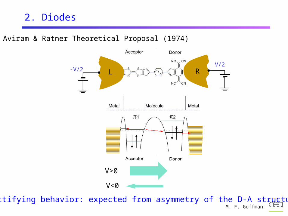
2. Diodes
Aviram & Ratner Theoretical Proposal (1974)
V>0
V<0
Rectifying behavior: expected from asymmetry of the D-A structure
-V/2 LV/2
R
M. F. Goffman
The Langmuir-Blodgett technique
Solution
eau
moléculesa
b
Single Molecular Film formation
Hydrophobic part
Transfer to a solid substrate
Special design of the molecule
M. F. Goffman
2. Diodes
Metzger et al.,JACS 119, 10455 (1997).
Al
Al
Experimental Realization
Spacer: -conjugated
Some differencesAviram & Ratner Metzeger et al
Spacer: -saturated
aliphatic chain (donor side)
Is Rectification due to the Aviram & Ratner mechanism ?
Answer: No!
M. F. Goffman
Which is the Rectification Mechanism
Aviram & Ratner
Spacer: -saturated Spacer: -conjugated
Metzeger et al
Donor and Acceptor molecular orbitals remain localized
LUMO
HOMO
DFT calcultion: HOMO and LUMO delocalized
M. F. Goffman
Rectification Mechanism: Asymmetric Coupling
Metzger et al.,JACS 119, 10455 (1997).
aliphatic chain (donor side) D A
10.1
l2 1
l
As a first approximation
Al
Al
D
A
Potential Profile
-V/2
V/2
r
V
-V/2
V/2
l
l
Asymetric Coupling can be used for fabricating Diodes.
M. F. Goffman
Using asymmetric coupling for Diode function
N. Lenfant et al., Nanoletters 3, 741 (2003).
-1.0 -0.5 0.0 0.5 1.0
-30
-20
-10
0
10
VT
Cur
rent
den
sity
(µA
.cm
-2)
Voltage (V)
-40
-20
0
20
40
-1 0 1
I (n
A)
COO
S
Thiophene
Si
O
OO
Substrate
(CH12)15
Si
O
OO
Substrate
(CH12)15
COO
Phenyl
Two step fabrication:Self-assembly of alkyl chains-conjugated groups
Control measurement on Alkyl chains
n-doped Silicon
Al Al
n-doped Silicon
M. F. Goffman
2. Diodes and NDR
N. P. Guisinger et al, Nanoletters 4, 55 (2004)
NDR behavior: due to resonance conditionsThe NDR bias varies by as much as 1 V from experiment to
experiment
M. F. Goffman
3. Switches
At least two different stable states different conductance (high /low)
Collier at al., Science 285, 391 (1999)Collier at al., Science 289, 11721 (2000)D. R. Stewart at al., NanoLett. 4, 133 (2004)
M. F. Goffman
Light-triggered Switches
0
0.5
1
1.5
2
2.5
3
250 350 450 550 650 750 850
open
closed
Switches in Toluene
Ab
sorp
tion
(nm)
Closed
Open
TypicallyCourtesy of D. Dulić and S.J. van der Molen
Does it work in a solid state device ?
M. F. Goffman
Breakjunction experiment
=546 nm
=313 nm
One way Photochromism
No switching back !?
Why closing is quenched?
OPEN QUESTION
D. Dulić et al, PRL 91,207402 (2003).
M. F. Goffman
Final Remarks
• Conductance properties of single molecules can be probed. However reproducibility and stability remains a challenge.
• More experiments are needed in order to refine theory and more theoretical calculation are needed to design interesting experiments (feedback!).
• Molecular Diodes can be obtained using asymetric coupling.
• Molecular Electronics on silicon can be a way of fabricating hybrid devices taking profit of the powerful infrastructure of the silicon-based IC industry Resonant tunneling devices.
• Light Triggered switches are promising molecules. Tuning of the coupling between the active part and the electrodes are needed to get reversible operation.
M. F. Goffman
MCBJs Results on Different Molecules (@4K)
-1500 -1000 -500 0 500 1000 1500
-200
0
200
400
OPV3 @ 4 K
I (nA
)
V (mV)-200 -100 0 100 200
-1.0
0.0
1.0
Experiment (10 sweeps) DFT Calc
Rin
g
Rin
g
C=
C
C=
C
C-H
op
C-H
op
d 2I/d
V 2 (
µA
.V -
2 )
V (mV)
High stability (>10 hs) at 4K
d2I/dV2 spectrum Fingerprint of the molecule ?
A. Isambert, D. Dulić, JP Bourgoin, M. F. Goffman, unpublished