First-principles study of boron sheets and nanotubes
Hui Tang and Sohrab Ismail-BeigiDepartment of Applied Physics, Yale University, New Haven, Connecticut 06520, USA
�Received 30 April 2010; published 8 September 2010�
Based on first-principles calculations, we present various properties of single- and double-layered boronsheets, along with single- and double-walled boron nanotubes. Single-layered boron sheets, made of hexagonsand triangles, have buckled ground-state geometries if the ratio of triangles to hexagons is large and stay flatotherwise. We demonstrate that this asymmetric behavior of buckling cannot be explained by a simple chemi-cal picture based on �-� mixing. Instead, reduction in the electronic kinetic energy is the driving force forbuckling. In addition, we show that double-layered boron sheets can form strong interlayer bonds between twolayers only if the precursor single-layered sheet itself prefers a buckled ground-state structure. The optimaldouble-layered boron sheet in our library is semiconducting and is more stable than any single-layered sheet.Next, we discuss the curvature energies, buckling behavior and soliton structural fluctuations for single-walledboron nanotubes and the implications for the electronic properties of these nanotubes: our main finding is thatthe semiconducting nature of small-diameter single-walled nanotubes is robust under various perturbations andfluctuations. We end by showing that due to strong bonds forming between walls, the optimal double-walledboron nanotubes have different wall structures from single-walled ones. Such double-walled nanotubes arealways more stable than any single-walled nanotube and are furthermore metallic for the likely experimentallyrelevant diameter range. We conclude with the implications of these results for fabricated nanotube systems.
The fifth element on the periodic table, boron, occupies aninteresting transitional position between nonmetallic andmetal elements. Boron compounds exist in the variety ofintriguing and peculiar geometric configurations. All the var-ied phases of pure boron crystals are composed of B12 icosa-hedra but can have complex structures linking these icosahe-dra to yield primitive unit cells with many atoms.1–6 Whilethe simplest phase, � rhombohedral boron, has 12 atoms perprimitive cell,1–3 there are approximately 106.67 atoms perprimitive cell in the � rhombohedral boron structure.3,4 Onepossible rationalization of this complex bonding behavior isthat boron is electron deficient so that boron crystals arestabilized by the mixing of two-center and three-centerbondings.1,4
Similar to boron crystals, nanostructures of boron alsoexhibit versatile morphology. Small boron clusters tend toform buckled two-dimensional �2D� quasiplanar disklikestructures made of triangular motifs7–15 and are aromatic inthe same manner as carbon molecules.12,16 Large boron clus-ters with more than 20 atoms prefer to roll up and form ringstructures with surfaces composed of triangularmotifs.15,17–19 Based on theoretical and experimental studieson such boron clusters with triangular structural motifs, re-searchers have predicted the existence of long one-dimensional boron nanotubes.20–24 In 2004, the first boronnanotubes were fabricated in experiments.25 Since then,single-walled boron nanotubes have been investigated inmany theoretical works using the buckled triangular sheet asthe precursor.26–30 These works predicted that single-walledboron nanotubes are always metallic with large densities ofstates around their Fermi energies and that the stability ofsuch boron nanotubes depends on both diameter and chiral-ity. Researchers have further shown that double-walled boron
nanotubes based on the buckled triangular sheet are morestable than their single-walled counterpart with bonds form-ing between inner and outer walls.31
In 2007, stable boron clusters in the form of boronfullerenes were theoretically predicted.32 These hollowspherical structures have surfaces composed of mixtures ofpentagons, hexagons, and triangles. Structures of these boronfullerenes are closely related to those of carbon fullerenes.For instance, the B80 fullerene can be constructed from theC60 structure by filling all 20 hexagon faces with extra at-oms. Separately, a large class of stable 2D boron sheets werefound.33,34 These boron sheets are made of hexagonal andtriangular motifs and are more stable than the buckled trian-gular sheet. The stability of these boron sheets is explainedthrough a balance between two-center bonding and three-center bonding.33 These discoveries have spurred further re-search work: various boron fullerenes have been studied andgeneral design rules to construct stable boron fullerenes andsheets have been proposed;35–38 small-diameter single-walledboron nanotubes haven been shown to be semiconductingdue to surface buckling;34,39 metal-doped boron fullerenesand nanotubes are proposed to be good candidates for hydro-gen storage;40,41 a route to construct stable metal boridenanostructures has been presented based on a self-dopingpicture for 2D boron sheets.38
In all these works, researchers have found out that surfacebuckling is a common phenomenon for boron nanostruc-tures. 2D quasiplanar boron clusters are always buckled.7–15
For 2D boron sheets, some are flat while others tend to haveground-state structures with buckled surfaces, e.g., the buck-led triangular sheet.26,28 Furthermore, although the moststable single-layered boron sheet is metallic, small-diametersingle-walled boron nanotubes made from it are semicon-ducting because of surface buckling.34,39 Finally, as we de-scribe below in Sec. IV, surface buckling is a critical deter-mining factor for stabilizing double-layered boron sheets. We
believe that clarifying the origin of this universal tendencytoward buckling is an important part of understanding thebehavior and stability of boron nanostructures. Therefore,our goals are to elucidate this particular issue.
Another important topic not yet thoroughly addressed inthe literature is the stability of double-walled boron nano-tubes: to date, most studies that we are aware of have fo-cused on single-walled nanotubes. It is an interesting andimportant question to see whether double-walled �or multi-walled� boron nanotubes are more stable than single-walledones. As we discuss in Sec. VI, stable double-walled boronnanotubes are possible with properties distinct from single-walled varieties.
The broad aims of this work are to use first-principlestheory to address the following: �a� to provide a detaileddiscussion of the stability of 2D single-layered boron sheetsand their buckling behavior, �b� to explain the physicalmechanism driving the buckling, �c� to explain the stabilityand buckling behavior of double-layered boron sheets, �d� toexamine the stability and buckling behavior of single-walledboron nanotubes, and �e� to describe the construction, stabil-ity, and physical properties of double-walled boron nano-tubes.
The paper is organized as follows. In Sec. II we describeour theoretical and computational approach. In Sec. III wepresent our results on atomically thin boron sheets, describethe asymmetric buckling behavior in this class of boronsheets, and explain the driving force for the buckling. In Sec.IV, we use the knowledge gained from the buckling behaviorof single-layered boron sheets to study the structure and sta-bility of double-layered boron sheets which leads us to aparticularly stable and semiconducting double-layered boronsheet. In Sec. V, we discuss the properties of single-walledboron nanotubes: their curvature energies, their buckling be-havior, the relation of their buckling to their electronic struc-tures and stability, and the role of structural fluctuations ontheir properties. In Sec. VI, we consider double-walled boronnanotubes constructed in three different ways and comparetheir relative and absolute stability and their electronic prop-erties to their single-walled cousins. We summarize and con-clude in Sec. VII.
II. METHODOLOGY
We calculate the electronic ground-state properties usingdensity-functional theory42,43 with the ab initio pseudopoten-tial total energy approach.44 Our results are obtained with thelocal density approximation �LDA� �Refs. 43 and 45� for theexchange and correlation interactions while the generalizedgradient approximation �GGA� �Ref. 46� is employed tocheck key results. Overall, our LDA and GGA results arevery similar with some minor quantitative differences. Weuse norm-conserving pseudopotentials generated by theTroullier-Martins scheme.47 The pseudopotential for boron isgenerated with the 2s22p13d0 reference configuration, withradial cutoffs �rc
s ,rcp ,rc
d�= �1.7,2.1,1.7�a0, and the d potentialis the local channel. To study boron sheets, supercells are setup to make sheets extended along x-y directions while peri-odic images along z direction have an distance of 10.6 Å
which is sufficient for studying isolated boron sheets. Forboron nanotubes, the tubes are extended with periodicboundary conditions along z while the lattice is square in thex-y plane where the distance between the outer walls of ad-jacent periodic copies of the tubes is at least 10.6 Å to en-sure that we study the limit of isolated nanotubes.
We use two different basis sets to deal with systems ofdifferent sizes. Two plane wave codes, PARATEC48 andPWSCF,49,50 are used for small systems with tens of atoms�mainly boron sheets�. A plane-wave-basis set with an energycutoff of 32 Ry is used to expand the electronic wave func-tions. For large systems with hundreds of atoms �mainly bo-ron nanotubes�, we calculate the ground-state properties withthe SIESTA code,51,52 for which numerical atomic orbitalswith double-� polarization are used to expand the single-particle wave functions, an equivalent plane-wave cut-off en-ergy 80 Ry is used to construct the real space mesh, and anenergy shift of 0.02 Ry is chosen to define the confined lo-calized orbitals. For either approach, K-point sampling forevery system converges total energies to better than 1 meV/atom and we use a Gaussian smearing width of 0.05 eV toperform all the K-space integrals. All systems are relaxeduntil atomic forces are smaller than 0.01 eV /Å and stressesare below 50 MPa. We have checked the results calculatedwith SIESTA versus PARATEC and PWSCF for small boronsheets and nanotubes. Compared to PARATEC and PWSCF, SI-
ESTA results show the same energetic trend and similar en-ergy differences for various structures in spite of differentabsolute binding energies. Structures are visualized with theXCRYSDEN code.53
III. SINGLE-LAYERED BORON SHEETS
A. Atomically thin single-layered boron sheets
Boron, the neighbor of carbon, displays versatile chemicalbonding when compared to carbon. As shown in our previ-ous work,33 boron sheets, the possible 2D precursors of bo-ron nanotubes, are composed of mixtures of triangular andhexagonal motifs. These sheet structures are stabilizedthrough the balance between two-center bonding in the hex-agonal regions and three-center bonding in the triangularregions.33 Therefore, the stability of boron sheets dependsstrongly on the ratio of hexagons to triangles, which is de-scribed by a “hexagon hole density” �.33 � changes from 0to 1/3 as boron sheets alter from the triangular sheet T�0��see Fig. 3�a�� to the hexagonal sheet H�1/3� �see Fig. 1�b��.The most stable boron sheet structure, sheet � or A�1/9� �seeFig. 3�c��, occurs at �=1 /9 due to the fact that electrons fillall the in-plane bonding states and leave all the in-plane an-tibonding states empty, which results from a prefect balanceof two-center bonding and three-center bonding.
In this work, the naming system for boron sheets involvesusing a letter followed by the � value to designate a single-layered sheet: T�0� is the flat triangular sheet, H�1/3� is thehexagonal sheet and A�1/9� is the most stable � sheet. Fordouble-layered boron sheets discussed mainly in Sec. IV, wename a sheet using the word “double” followed by the nameof the corresponding precursor single-layered sheet. For in-stance, double-B�1/7� refers to a double-layered boron
HUI TANG AND SOHRAB ISMAIL-BEIGI PHYSICAL REVIEW B 82, 115412 �2010�
115412-2
sheet made from stacking two identical B�1/7� sheets �seeFig. 5�b��.
Besides �, the stability of boron sheets also depends onthe distribution of hexagons. Full exploration of this degreeof freedom obviously leads to an infeasible and combinato-rially large search. However, to achieve an understanding ofthe basic effects, we study the two extremes: either the hexa-gons are as evenly distributed as possible �e.g., sheet A�1/9��or the hexagons are packed linearly to form lines �e.g., Fig.1�c��. For any sheet, we define the binding energy per atomas
Eb = Eat − Esheet, �1�
where Eat is the energy of an isolated spin-polarized boronatom and Esheet is the energy per atom of a sheet. By definingthe binding energy this way, larger binding energies corre-spond to more stable structures.
Figure 1 shows the LDA Eb of flat sheets versus � forboth extremes. For even distribution, Eb reaches maximum at�=1 /9 which corresponds to sheet A�1/9�. For the linearlyaligned hexagons, the most stable structure occurs at �=1 /7, which is 0.03 eV/atom less stable than sheet A�1/9�.Although sheets with hexagon lines are more stable for ��1 /5, boron sheets with evenly distributed hexagons aremore favorable for � close to 1/9. In this work, since weconcentrate primarily on the most stable boron nanostruc-tures, we will be primarily interested in studying the proper-ties of boron sheets with evenly distributed hexagons. In fol-lowing sections, all boron sheets have hexagons evenlydistributed unless noted specifically.
B. Asymmetry of buckling in boron sheets
Unlike graphene, not all 2D atomically thin boron sheetsare completely flat. Instead, for many boron sheets, the at-oms prefer to move out of the nominal sheet plane and formcorrugated surfaces. This phenomenon is generally named“buckling” in the literature. Buckling is quite common inboron nanostructures. All quasiplanar boron clusters studiedin both theory and experiments have buckled surfaces.7–15
For 2D boron sheets made of triangles and hexagons, theground-state configurations may be either buckled or flat de-pending on the hexagon-to-triangle ratio �see below�. In ad-dition, small-diameter nanotubes have buckled surfaces34,39
although their precursor, sheet A�1/9�, prefers to stay flat.Finally, buckling is closely related to the formation of inter-layer bonds in double-layered boron sheets as we discuss inSec. IV. For these reasons, investigating the buckling of bo-ron sheets is helpful for understanding the basic properties ofboron nanostructures.
We have performed a large number of calculations on 2Dsingle-layered boron sheets where we start with flat configu-rations, create perturbations in the form of buckling of thesurfaces, and allow for full relaxations. We summarize thekey results here. First, for sheets with �1 /5, which in theirflat form are already highly unstable compared to the optimalsheets with ��1 /9 �see Fig. 1�, we find large vertical buck-ling amplitudes along the out-of-plane �z� direction and com-plex resulting final structures. However, even after relax-ation, these structures are still quite unstable energetically sowe ignore them in what follows. Second, for sheets with �1 /5, some sheets buckle vertically along the out-of-plane zdirection while some do not and remain flat. More precisely,among boron sheets with evenly distributed hexagons andfor 0�1 /5, we find that whether the ground state isbuckled or flat depends only on the hexagon hole density �.The buckling behavior is asymmetric with respect to �:sheets with �1 /9 prefer to buckle while those with ��1 /9 remain flat. The energetic changes due to buckling areshown in Fig. 2. The increase in stability due to buckling isat most 0.16 eV/atom for the triangular T�0� sheet and de-creases to zero as �=1 /9 is approached. The separationpoint occurs at �=1 /9, which coincides with the optimalsheet structure A�1/9�. Therefore, when we account for thebuckling effect, the left side ��1 /9� of the binding energycurve becomes somewhat flatter as shown in Fig. 2.
It has been known that the triangular sheet T�0� �see Fig.3�a�� can buckle in many different ways and get trapped invarious local minima but the two-atom-cell buckling patternleads to the most stable structure of the buckled triangularsheet.26–30,33 However, for other sheets with 0�1 /9, wefind that they generally prefer to become buckled in somespecific manner. These buckling patterns are determined bythe eigenvectors of the unstable phonon modes with imagi-nary frequencies of the corresponding flat sheets. For in-stance, the �=1 /12 sheet Z�1/12� shown in Fig. 3�b� has twodifferent buckling patterns determined by its two imaginaryphonon modes. One of these patterns is shown in Fig. 3�b� asindicated by coloring. The stabilization of the buckled Z�1/12� sheet is actually quite small and is only 0.01 eV/atom.
On the other hand, the optimal A�1/9� and other sheetswith 1 /9�1 /5 �e.g., sheets B�1/7� and C�1/6� in Fig. 3�
FIG. 1. �Color online� �a� Binding energy Eb �from LDA� versushexagon hole density � for flat single-layered boron sheets in twoextreme cases. The blue “�” are the calculated binding energies forthe case where hexagons are evenly distributed. The red “�” are thecalculated binding energies for the case where hexagons form lines.The solid curves are polynomial fits to guide the eye. �b� Top viewof the hexagonal sheet H�1/3�. �c� An example of boron sheets withlines of hexagons. For �b� and �c�, the red solid lines show theprimitive unit cells. Gray balls are boron atoms and sticks connectnearest-neighbor atoms.
FIRST-PRINCIPLES STUDY OF BORON SHEETS AND… PHYSICAL REVIEW B 82, 115412 �2010�
115412-3
have only stable positive phonon frequencies and thus stayflat. In order to see whether these sheets prefer to bucklewhen compressed, which is typical when they are bent orcurved to form part of a nanotube, we studied these flatsheets under isotropic compression in the x-y plane andchecked to see if any phonon became unstable. Not surpris-ingly, we found that under sufficient compression, everysheet will develop one or more imaginary phonon frequen-cies and will buckle. For example, sheet B�1/7� has an imagi-nary phonon frequency once compressed by 5%. The buck-ling patterns of compressed sheets A�1/9�, B�1/7�, and E�1/6�are shown in Fig. 3 by coloring.
C. Origin of buckling: �-� mixing?
What is the origin of this common tendency for 2D boronstructures to buckle? An obvious first guess is that perhapsthe buckling is driven by mixing of in-plane � and out-of-plane � states. For a flat 2D structure, all electronic stateshave either even or odd parity with respect to the reflectionin the plane which corresponds to in-plane ��� and out-of-plane ��� states, respectively. Once a 2D structure becomesbuckled, the original reflection symmetry is lost, and in aperturbative picture the resulting electronic states are mix-tures of the original in-plane and out-of-plane states. If im-portant mixing happens around the Fermi level, bondingcombinations of � and � states could be pushed below theFermi level leading to increased stability. �This picture isanalogous in many ways to the stabilization coming from aPeierls distortion.� In other words, in this scenario the bandenergy would decrease sufficiently to overcome the increasein elastic energy and thus make buckling preferable.
Following this idea, the fact that sheet A�1/9� is flat can berationalized via a simple argument: no mixing between in-plane and out-of-plane states exists around the Fermi energybecause the Fermi level lies in an energy gap for the in-planestates.33 Thus there is no energy gain to compensate the in-crease of elastic energy. However, this explanation is already
problematic because it does not provide a reason for the clearasymmetry in buckling behavior around �=1 /9. All sheetswith � above and below 1/9 have in-plane and out-of-planestates coexisting at the Fermi energies so that we would haveexpected that sheets on both sides of �=1 /9 would buckle indisagreement with the ab initio results.
A more careful examination shows that in fact the entirepicture is quantitatively incorrect. �A better explanation isprovided in the next section.� To examine whether the behav-ior of the band energy can explain the buckling, we dividethe total energy Etot into two parts, the band energy Eband andthe remainder as a “repulsive” term Erep
Etot = Eband + Erep, �2�
where
0 0.1 0.2 0.3Hexagon hole density η
5.8
6
6.2
6.4
6.6
6.8
Bin
ding
ener
gy(e
V/a
tom
)
1/3
η=1/9
Buckled Flat
Complexunstablestructrues
FIG. 2. �Color online� Binding energy Eb �from LDA� versushexagon hole density � for single-layered boron sheets with evenlydistributed hexagons. The blue “�” are the binding energies of flatsheets and the solid blue curve is a polynomial fit. The green “�”are the binding energies for buckled sheets �that are stabilized bybuckling�. Maximal Eb occurs for sheet � ��=1 /9� or A�1/9�,which is the most stable structure. The vertical dashed red line at�=1 /9 indicates the separation point of naturally flat and buckledsingle-layered boron sheets.
FIG. 3. �Color online� Structures of five boron sheets: �a� T�0�,�b� Z�1/12�, �c� A�1/9�, �d� B�1/7�, and �e� C�1/6�. The red solidlines show the unit cells. The preferred buckling patterns are indi-cated by coloring: z coordinates increase as color changes fromgreen to gray to purple so that green means negative z coordinates,gray shows z coordinates close to 0, and blue means positive z.Since the sheets A�1/9�, B�1/7�, and C�1/6� do not buckle at equi-librium, the buckling patterns shown here are obtained by applyingan isotropic compressive strain of 5% in the x-y plane.
HUI TANG AND SOHRAB ISMAIL-BEIGI PHYSICAL REVIEW B 82, 115412 �2010�
115412-4
Eband = �−�
EF
D�E�EdE , �3�
where D�E� is the electronic density of states and EF is theFermi energy, and we compute this energy directly from thefirst-principles results. The repulsive energy, Erep=Etot−Eband, is defined and computed exactly as this differencefrom ab initio calculations. �To make Erep always positive,we have defined the repulsive energy of an isolated boronatom to be zero, then Erep and Etot for all boron sheets arescaled accordingly.� As expected from simple tight-bindingtheory, Erep is generically positive and in a tight-binding pic-ture would be given by a sum over repulsive pairinteractions54
Erep � �Ri,Rj
V��Ri − Rj�� , �4�
where V��Ri−Rj�� is a short-range repulsive interaction be-tween two nuclei at Ri and Rj. �However, we emphasize thatwe do not use this approximate form but instead computeEtot, Eband, and Erep directly from the first-principles results.�
When computing the band energy, it is clear that anyshifts in EF will modify the computed value. It is well knownthat standard periodic supercell calculations have an arbi-trary, and difficult to compute, energy shift stemming fromthe long-range Coulomb interaction. Therefore, to get reli-able Eband energies, we must measure EF with respect to thevacuum level. This is accomplished by performing a series ofcalculations with differing supercell sizes L along the z di-rection; the behavior of EF versus L for large L is essentiallylinear in L−1. In this way, we can extrapolate to L=� and findabsolute EF and thus Eband energies.
In the �-� mixing picture described above, the band en-ergy Eband should decrease upon buckling as hybridizationaround EF pushes states below EF. In Table I, we show thecalculated band energies and repulsive energies of five sheetsspanning a range of � values when they are flat and slightlybuckled �according to their preferred buckling patterns�, re-spectively. We can see that all sheets except sheet C�1/6�have their band energies increase and repulsive energies de-crease due to buckling, while sheet C�1/6�, which naturallydoes not prefer to buckle, has the opposite behavior. These
results are clearly opposite to the expectations from the �-�mixing picture. In other words, splitting the total energy intoband and repulsive energies has not helped us understand theorigin of the buckling.
D. Kinetic energy: The driving force for buckling
As the chemical bonding picture based on �-� hybridiza-tion fails to explain the buckling, we turn to a differentphysical picture. We instead view these 2D metallic boronsheets as a realization of �a possibly nonstandard� 2D elec-tron gas. Namely, we should consider breaking up the totalenergy into terms that are most natural for an electron gasanalysis: the kinetic energy, the �classical� electrostatic en-ergy of interaction among all charges, and the exchange-correlation energy due to the quantum behavior of the elec-trons. Interestingly, even though 2D boron sheets showsignificant covalent bonding character, this picture turns outto work well: the kinetic term is dominant, as expected for amedium-to-high-density electron gas, and its variationslargely dictate the buckling. Therefore, we write the totalenergy Etot as
Etot = Ekin + Exc + Ees, �5�
where Ekin is the total electronic Kohn-Sham kinetic energy,Exc is the exchange-correlation energy �here evaluated withinthe LDA or GGA�, and Ees is the sum of all remaining ener-gies. Ees physically represents the sum of all classical elec-trostatic interactions among charges: electron-electron,electron-ion, and ion-ion. �The nonlocal electron-ion interac-tion from the pseudopotential is thus included in Ees as thisterm is designed to reproduce the interactions of the valenceelectrons with the nucleus in an all-electron framework.�
Separately, it is helpful to have a measure of the averageelectron density in the system in order to correlate with usualnotions of electron gas behavior. Unfortunately, there isno obvious unique a priori way to define an average electrondensity for an arbitrary material system with a spatiallyvarying electron density. Therefore, we resort to a verysimple definition which uses the density itself as the weigh-ing function
TABLE I. Band energies �Eband�, repulsive energies �Erep�, and total energies �Etot� of five boron sheetsT�0�, Z�1/12�, A�1/9�, B�1/7�, and C�1/6�, respectively, for flat and buckled cases �from LDA�. For the flatsheets, the energies are in eV/atom. For the buckled sheets, the percentage change from the flat energy isreported to highlight the direction of the energy change �“+” for increase and “−” for decrease�. The bucklingheight is fixed at 0.16 Å in all cases.
Sheet
Flat Buckled
Eband Erep Etot �Eband �Erep �Etot
T�0� −37.82 8.50 −29.32 +0.89 −4.31 −0.10
Z�1/12� −37.21 7.68 −29.54 +1.19 −5.81 −0.01
A�1/9� −36.21 6.61 −29.59 +0.59 −3.18 +0.01
B�1/7� −35.07 5.52 −29.55 +0.92 −5.00 +0.02
C�1/6� −33.89 4.38 −29.51 −0.02 +0.68 +0.01
FIRST-PRINCIPLES STUDY OF BORON SHEETS AND… PHYSICAL REVIEW B 82, 115412 �2010�
115412-5
n̄ =� �n�r��2dr
� n�r�dr
. �6�
This simple measure averages the density in the spatial re-gions where the electrons spend the most time. Therefore, itis biased to large values by the relatively large values of theelectron density close to each boron atom and does not onlymeasure the electron density of the delocalized mobile elec-trons. However, for our purposes, it is a reasonable definitionin which it shows monotonic behavior versus � �see below�.
We first investigate how Ekin, Exc, and Ees behave for flatsheets. Figure 4 shows Ekin, Exc, and Ees versus � for a largeset of flat 2D boron sheets. We can see that Ekin, Exc, and Eesall change smoothly and monotonically with � or equiva-lently with 1-�. Because the nearest neighbor distances inthe different boron sheets are almost identical,33 for these flatsheets 1-� also changes monotonically with the averageelectron density n̄ as shown in Table II. Hence, Ekin, Exc, andEes all change monotonically with n̄ as one would expect foran electron gas.
We now turn to the buckling effect for these sheets. TableII shows how Ekin, Exc, and Ees change when each sheetbuckles. For the five sheets investigated, Ekin always de-creases and Exc and Ees always increase due to buckling. Forthose sheets that prefer to buckle, sheets T�0� and Z�1/12� inTable II, the decrease in Ekin dominates over the other twoenergy increases. Therefore, the buckling is driven by kineticenergy lowering and that kinetic energy lowering wins overthe increase of Ees+Exc for �1 /9. In addition, we see thatn̄ is decreased by buckling, and lowering of density is con-sistent with lowering of kinetic energy �a smaller Fermi mo-mentum or Fermi energy� and higher Ees and Exc �largeraverage charge separation�. Intuitively, if we view the sheetas a continuous film, then surface buckling can be expectedto increase the surface area which then rationalizes the de-crease in electron density: the same number of electrons arespread over a sheet with increased surface area due to thecorrugation. However, since there is no rigorous definition ofsurface area at the discrete atomic scale, this picture servesprimarily as an aide to understanding and visualization.
What we have found is that buckling reduces the electrondensity which in turn lowers the kinetic energy and thusdrives the buckling. The kinetic energy is larger and moredominant for higher electron densities �smaller �� so thatthose sheets will have a stronger tendency to buckle. Mostimportantly, this picture naturally explains the asymmetry inthe buckling behavior about �=1 /9. Since buckling reducesn̄, and n̄ and 1−� are in monotonic relation, decreasing n̄effectively increases �. Because the binding energy versus ��see Fig. 1� has a maximum at �=1 /9, sheets with �1 /9can increase their stability by buckling while those with �1 /9 would decrease their stability if they buckled.
The above results clearly show that it is the lowering ofthe kinetic energy that drives the initial stages of buckling inboron sheets. We may wonder if this finding is more general.After all, for the small buckling amplitudes used above, itcan be argued that the geometry and chemical bondingmodes barely change but in the final fully buckled structurethis may not be the case. For example, the fully buckledtriangular sheet has strong two-center-type bonding and thebond length along that direction are significantly reduced26,27
pointing to basic changes in bonding topology and possibly adecrease in surface area in the intuitive picture above. How-
0 0.1 0.2 0.3Hexagon hole density η
-8
-4
0
4
8
∆E(e
V/a
tom
)
Ekin
Ees
Exc
1/3
FIG. 4. �Color online� Kinetic �Ekin�, electrostatic �Ees�, andexchange-correlation �Exc� energies versus � for flat 2D boronsheets. Energies are in the units of eV/atom. All three energies areplotted with respect to their respective values at �=0 �the zero ofenergy�. The squares, circles, and diamonds are the calculated re-sults while the solid curves are guides to the eye.
TABLE II. Kinetic energy �Ekin�, electrostatic energy �Ees�, exchange-correlation energy �Exc�, total energy �Etot�, and the averageelectron density n̄ of five boron sheets T�0�, Z�1/12�, A�1/9�, B�1/7�, and C�1/6�, respectively, for flat, artificially buckled and fully relaxedcases �from LDA�. For flat sheets, energies are in eV/atom and n̄ is in units of 10−2 e /Bohr3. For buckled and fully relaxed sheets, we showpercentage changes of the energies and n̄ compared to the flat values �+ for increase, − for decrease�. The buckling height is fixed at 0.16 Åin all artificially buckled sheets.
Sheet
Flat Buckled Fully relaxed
Ekin Ees Exc Etot n̄ �Ekin �Ees �Exc �Etot �n̄ �Ekin �Ees �Exc �Etot �n̄
HUI TANG AND SOHRAB ISMAIL-BEIGI PHYSICAL REVIEW B 82, 115412 �2010�
115412-6
ever, our results show that even in fully relaxed buckledsheets, the kinetic energy is still the energetic driving force:Table II shows that for the triangular T�0� and the Z�1/12�sheets, the kinetic energy and average electron density arealways lowered compared to their flat counterparts—and thisholds for other sheets we have investigated. Furthermore, aswe will show in Sec.V B, the same kinetic energy reductionholds for buckled single-walled boron nanotubes as well.Therefore, we believe that kinetic energy reduction is mostprobably the key driving force for the buckling of boronsheets and nanotubes.
IV. DOUBLE-LAYERED BORON SHEETS
For boron nanostructures, strong interlayer bonds can beformed between two planar or quasiplanar parts stacking per-pendicular to the nominal structure plane.31,55 Due to theseinterlayer bonds, multilayered boron sheets can be more en-ergetically favorable than the most stable single-layered bo-ron sheet A�1/9� �see below�. When creating boron nano-structures such as nanotubes by folding, wrapping, or cuttingboron sheets, it is possible that multilayered boron sheetswill be the parent structures under certain growth conditions.Therefore, studying multilayered boron sheets, where thesimplest cases are those of double-layered sheets, can berelevant to understanding experimentally grown structures aswell as to helping us understand the general properties forboron nanostructures.
Below, we find that the knowledge we have gained�above� concerning the buckling of single-layered boronsheets is invaluable in clarifying and rationalizing the ten-dencies for buckling and formation of interlayer bonds indouble-layered systems. In this work, we limit ourselves todouble-layered sheets which already create a large class ofsystems to study and analyze. Our primary aim is to obtain abasic understanding of the buckling and bonding behavior ofboron sheets when they are in close proximity. An extensionof these results to multilayered structures is beyond the scopeof the present work.
To study double-layered boron sheets, we proceed in thefollowing manner: we take two �primitive cell� copies of aparticular 2D boron sheet and place the two copies someinitial distance apart ��3 Å�. We then create some randomperturbations of all atomic positions and perform a full re-laxation. After following this procedure for a large number ofsuch double-layered structures, we discover that a pair ofsheets with �1 /9 tend to make strong interlayer bonds. Onthe other hand, two sheets with � 1 /9 do not: the twosingle-layered sheets stay quite flat, are weakly bound, andstay apart at a relatively large distance of typically3.5–3.6 Å. �This separation likely correlates with weak vander Waals interactions which are not correctly captured byLDA or GGA calculations; however, our main point is thatthe interactions are quite weak and no interlayer bonds areformed which we believe is a robust result even if van derWaals interactions were included correctly.� Two typical ex-amples are shown in Fig. 5. When interlayer bonds form, theinterlayer bond length is about 1.7 Å which is quite typicalof the lengths in 2D boron structures.
The above behavior is simply explained from bucklingbehavior of single-layered boron sheets: a pair of sheets willform interlayer bonds only when each sheet alone prefers tobuckle in the first place �i.e., both sheets have �1 /9�. Themain requirement is to properly align the sheets so that thegeometry allows the buckling atoms to make interlayerbonds with each other. As a simple further test of the relationbetween buckling and formation of interlayer bonds, weknow that the optimally stable A�1/9� sheet does not nor-mally buckle but can be forced to buckle when under com-pression. Therefore, we put 1% of isotropic compression inthe xy plane on a pair of A�1/9� sheets in close proximity andfind that the sheets buckle, that they form interlayer bonds ofabout 1.7 Å in length, and that the bonding pattern is the onedictated by the buckling pattern of the single-layered sheetunder compression �see Fig. 3�.
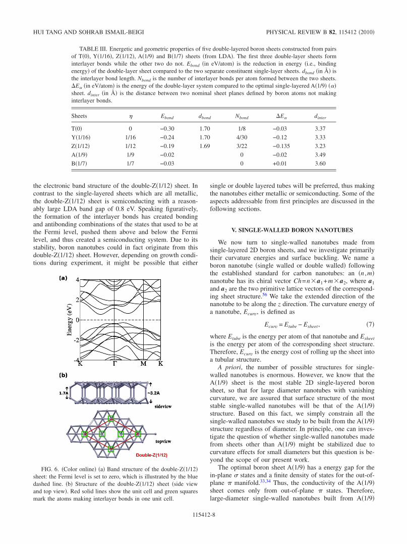
Table III shows a subset of our ab initio results fordouble-layered boron sheets built from pairs of T�0�, Y�1/16�, Z�1/12�, A�1/9�, and B�1/7� sheets. The first threedouble-layered sheets, made from T�0�, Y�1/16�, and Z�1/12�, form interlayer bonds with the bond lengths close to1.7 Å and thus strongly stabilize �i.e., bind� the double-layersystem. The energy reduction due to the interlayer bonding,Ebond in the Table, is significant and gets larger for smaller �since more interlayer bonds form. As a result, we find thatthe most stable double-layered sheet in our library occurs at�=1 /12 for the double-Z�1/12� case. This double-layeredsystem is 0.135 eV/atom more stable than the optimal single-layered A�1/9� sheet and is the most stable sheet structure wehave found to date. Figure 6 shows the atomic structure and
FIG. 5. �Color online� Illustration of structures of double-layered boron sheets �top and side views� for both �a� the �1 /9double-Y�1/16� sheet and �b� the �1 /9 double B�1/7� sheet. Thered solid lines in the top views show the 2D primitive unit cells.The green squares in the top view of �a� mark the atoms that forminterlayer bonds in a primitive cell.
FIRST-PRINCIPLES STUDY OF BORON SHEETS AND… PHYSICAL REVIEW B 82, 115412 �2010�
115412-7
the electronic band structure of the double-Z�1/12� sheet. Incontrast to the single-layered sheets which are all metallic,the double-Z�1/12� sheet is semiconducting with a reason-ably large LDA band gap of 0.8 eV. Speaking figuratively,the formation of the interlayer bonds has created bondingand antibonding combinations of the states that used to be atthe Fermi level, pushed them above and below the Fermilevel, and thus created a semiconducting system. Due to itsstability, boron nanotubes could in fact originate from thisdouble-Z�1/12� sheet. However, depending on growth condi-tions during experiment, it might be possible that either
single or double layered tubes will be preferred, thus makingthe nanotubes either metallic or semiconducting. Some of theaspects addressable from first principles are discussed in thefollowing sections.
V. SINGLE-WALLED BORON NANOTUBES
We now turn to single-walled nanotubes made fromsingle-layered 2D boron sheets, and we investigate primarilytheir curvature energies and surface buckling. We name aboron nanotube �single walled or double walled� followingthe established standard for carbon nanotubes: an �n ,m�nanotube has its chiral vector Ch=n�a1+m�a2, where a1and a2 are the two primitive lattice vectors of the correspond-ing sheet structure.56 We take the extended direction of thenanotube to be along the z direction. The curvature energy ofa nanotube, Ecurv, is defined as
Ecurv = Etube − Esheet, �7�
where Etube is the energy per atom of that nanotube and Esheetis the energy per atom of the corresponding sheet structure.Therefore, Ecurv is the energy cost of rolling up the sheet intoa tubular structure.
A priori, the number of possible structures for single-walled nanotubes is enormous. However, we know that theA�1/9� sheet is the most stable 2D single-layered boronsheet, so that for large diameter nanotubes with vanishingcurvature, we are assured that surface structure of the moststable single-walled nanotubes will be that of the A�1/9�structure. Based on this fact, we simply constrain all thesingle-walled nanotubes we study to be built from the A�1/9�structure regardless of diameter. In principle, one can inves-tigate the question of whether single-walled nanotubes madefrom sheets other than A�1/9� might be stabilized due tocurvature effects for small diameters but this question is be-yond the scope of our present work.
The optimal boron sheet A�1/9� has a energy gap for thein-plane � states and a finite density of states for the out-of-plane � manifold.33,34 Thus, the conductivity of the A�1/9�sheet comes only from out-of-plane � states. Therefore,large-diameter single-walled nanotubes built from A�1/9�
TABLE III. Energetic and geometric properties of five double-layered boron sheets constructed from pairsof T�0�, Y�1/16�, Z�1/12�, A�1/9� and B�1/7� sheets �from LDA�. The first three double-layer sheets forminterlayer bonds while the other two do not. Ebond �in eV/atom� is the reduction in energy �i.e., bindingenergy� of the double-layer sheet compared to the two separate constituent single-layer sheets. dbond �in � isthe interlayer bond length. Nbond is the number of interlayer bonds per atom formed between the two sheets.�E� �in eV/atom� is the energy of the double-layer system compared to the optimal single-layered A�1/9� ���sheet. dinter �in � is the distance between two nominal sheet planes defined by boron atoms not makinginterlayer bonds.
Sheets � Ebond dbond Nbond �E� dinter
T�0� 0 −0.30 1.70 1/8 −0.03 3.37
Y�1/16� 1/16 −0.24 1.70 4/30 −0.12 3.33
Z�1/12� 1/12 −0.19 1.69 3/22 −0.135 3.23
A�1/9� 1/9 −0.02 0 −0.02 3.49
B�1/7� 1/7 −0.03 0 +0.01 3.60
FIG. 6. �Color online� �a� Band structure of the double-Z�1/12�sheet: the Fermi level is set to zero, which is illustrated by the bluedashed line. �b� Structure of the double-Z�1/12� sheet �side viewand top view�. Red solid lines show the unit cell and green squaresmark the atoms making interlayer bonds in one unit cell.
HUI TANG AND SOHRAB ISMAIL-BEIGI PHYSICAL REVIEW B 82, 115412 �2010�
115412-8
will always be metallic since the electronic structures aredetermined by the zone-folding technique.56,57 However, ithas been found that small-diameter boron nanotubes builtfrom the A�1/9� sheet are semiconducting, with energy gapsaround a few tenth of eVs, due to curvature and surfacebuckling.34,39 Below, we investigate in detail these curvatureeffects on the energetics and electronic structures of thesingle-walled nanotubes.
A. Curvature energy
Figure 7 shows how the curvature energy Ecurv changeswith tube diameter D for a wide range of such achiral single-walled nanotubes �i.e., �n ,0� and �n ,n� nanotubes� createdfrom wrapping the A�1/9� sheet. The data from these twodifferent classes of nanotubes lie almost exactly on the samesmooth curve, suggesting that the curvature energy of thistype of single-walled nanotubes does not depend strongly onchirality. Namely, Ecurv is determined by the nanotube diam-eter D, a result that is consistent with previous works on thisproblem.34,39
As is the case for carbon nanotubes,58,59 we expect fromelastic theory that Ecurv should have the following simpledependence on D for large D:
Ecurv =C
D2 , �8�
where C is a constant. By fitting all the data in Fig. 7, weobtain C=4.28 eV Å2 /atom, slightly larger than the valueC=3.64 eV Å2 /atom in previous work,39 which we believeis due to the fact that the LDA we use usually results instronger bonding than GGA-PBE �Ref. 46�. For comparison,carbon nanotubes have C=8.56 eV Å2 /atom.58,59 Therefore,for a given diameter, it is easier to curve the A�1/9� sheetthan to curve graphene to create single-walled nanotubes.
B. Surface buckling under large curvature
Since sheet A�1/9� is metallic with a large density ofstates at its Fermi energy coming from the out-of-plane �manifold, simple zone folding leads us to expect that all
boron nanotubes made of sheet A�1/9� are metallic. How-ever, boron nanotubes with small radii are actually semicon-ducting due to the fact that tube surfaces become buckledunder the large curvature necessitated by the small diameter.This buckling has been attributed to rehybridization in the�-� manifold.34,39
As we explained in Sec. III B, sheet A�1/9� prefers to stayflat when it is stress free but will buckle under compression.When it buckles, the two boron atoms in each unit cell thatare in the triangular regions will move out of the sheet planewith one going up and the other going down �see Fig. 3�. Wefind that when the A�1/9� sheet is curved to form nanotubes,the same buckling pattern is observed: the two atoms in thetriangular regions become inequivalent with one moving ra-dially inward and the other moving radially outward. Due tothis surface buckling, small-diameter single-walled boronnanotubes become semiconducting. Figure 8 shows thesingle-walled nanotube �3,0� as an example. This bucklingand semiconducting behavior is only relevant for small di-ameter nanotubes: as Fig. 9 shows, the band gap vanishes fordiameters larger than 20 Å.34,39 We also see that for afixed diameter, the band gaps for �n ,0� and �n ,n� nanotubescan be significantly different.
As our results in Fig. 9 show, the LDA and GGA result insystematically different band gaps for these single-walledboron nanotubes with results that differ by 0.1–0.2 eV forthe same nanotube index. However, since LDA and GGAgive very similar band-gap predictions for bulk materials, thedifference is most likely not due to the treatment of exchangecorrelation but instead coming from a structural difference.In fact, the GGA generally predicts a larger surface bucklingfor single-walled nanotubes than LDA �see Table V�. There-fore, we plot the same data versus the buckling amplitude
0 5 10 15 20 25 30D(Å)
0
0.05
0.1
0.15
0.2
Ecu
rve(e
V/a
tom
)(n,0) type(n,n) type
E = 4.28D-2
FIG. 7. �Color online� Curvature energies Ecurv in eV/atom ofsingle-walled boron nanotubes made of the A�1/9� sheet versus di-ameter D in Å �from LDA�. Green “�” are for �n ,0� nanotubeswith n ranging from 3 to 14. Magenta � are for �n ,n� nanotubeswith n ranging from 3 to 9. The indigo solid line is a single-parameter 1 /D2 fit to the combined data set.
FIG. 8. �Color online� Structures �side view and top view� andband structures of the single-walled boron nanotube �3,0� with flat�left� and buckled �right� surfaces �from LDA�. Red dashed linesshow the Fermi energies.
FIRST-PRINCIPLES STUDY OF BORON SHEETS AND… PHYSICAL REVIEW B 82, 115412 �2010�
115412-9
instead of diameter in Fig. 9—the buckling amplitude is thedifference in radial distance of the two types of buckled tri-angular atoms. We see an approximate collapse of the dataon a single curve for both �n ,0� and �n ,n� nanotubes. There-fore, we believe that to leading order, the band gap for asingle-walled nanotube is determined by its buckling ampli-tude, while the relation of the buckling amplitude to the di-ameter is more complex but secondary.
To understand the surface buckling in more detail, wehave compared the properties of the buckled ground state of
a single-walled nanotube to the same nanotube but with a flatsurface. The flat structure is constructed as follows: we knowthat the atoms that buckle are those corresponding to theatoms of the parent A�1/9� sheet that are in a triangular re-gion. The symmetry breaking leading to the ground state hasone of these atoms move inward and the other move out-ward. To generate the flat structure, we simply force thesetwo atoms to remain equivalent by doing a constrainedatomic relaxation whereby we constrain these two atoms tohave the same radius measured from the nanotube axis. Asexpected, for flat surfaces, the single-walled boron nanotubesare all metallic regardless of diameter �e.g., see �3,0� nano-tube in Fig. 8�. Table IV shows the changes in different com-ponents of the total energy of buckled single-walled boronnanotubes compared to flat ones. For all nanotubes, bucklingis always accompanied by a decrease in kinetic energy Ekinand increases in Exc and Ees, the same as for 2D boronsheets. This strongly suggests that surface buckling in single-walled boron nanotubes is also driven by lowering of kineticenergy.
The total energy differences between flat and bucklednanotubes are found in Tables IV and V. The energy differ-ences per atom are extremely small and decrease to zerorapidly with increasing nanotube diameter: they are at most15 meV/atom for the smallest diameters. We note that theGGA systematically favors buckled surfaces compared to theLDA and predicts larger energy gains from buckling. Giventhe extremely small magnitude of these energy differences, itis not clear whether the LDA or GGA is accurate enough tocapture them correctly. In fact, a recent work60 has investi-gated the geometry of a finite �5,0� single-walled boronnanotube segment using the presumably more accurate MP2method61 and concluded that no buckling exists on the sur-face of this finite nanotube because the buckled configurationhas a higher energy. This is in contrast to our results here andprevious LDA- and GGA-based findings.34,39 Hence, we be-lieve that more caution is required regarding the LDA/GGA
FIG. 9. �Color online� Band gap Eg �in eV� versus tube diameter�top, in � and buckling amount �bottom, in � for �n ,0�- and�n ,n�-type A�1/9�-derived single-walled boron nanotubes calculatedwith both LDA and GGA.
TABLE IV. Kinetic energy �Ekin�, exchange-correlation energy �Exc�, electrostatic energy �Ees�, totalenergy �Etot� for flat- and buckled-surfaced single-walled boron nanotubes made of sheet A�1/9� based onLDA calculations using SIESTA. For flat cases, energies are in eV/atom. For buckled ones, we show percent-age changes of the energies compared to the corresponding flat values �+ for increase, − for decrease�.
HUI TANG AND SOHRAB ISMAIL-BEIGI PHYSICAL REVIEW B 82, 115412 �2010�
115412-10
predictions for such small energy differences and that furtherstudies are required to determine the correct ground-state ge-ometries and electronic properties of single-walled boronnanotubes made from the A�1/9� sheet. However, if surfacebuckling does in fact take place, the generic monotonic trendof decreasing buckling and decreasing gap with increasingdiameter is most likely a robust result. In the next section, wediscuss fluctuations in surface buckling assuming that theLDA/GGA predictions for the buckling are valid.
C. Fluctuations in buckling
The fact that small diameter nanotubes constructed fromthe A�1/9� sheet are semiconducting is a symmetry breakingphenomenon: the surface of the nanotube buckles in a waythat two originally equivalent atoms �per surface unit cell�become inequivalent whereby one moves radially inwardsand the other outward. The existence of two distinct butsymmetry-related minima, i.e., a degenerate ground state, al-lows for the possibility of topological soliton fluctuations atfinite temperatures that connect one minimum to the other. Atopological soliton represents a stable, nonuniform distribu-tion of an order parameter �surface buckling here� that occursin a system with several degenerate ground-state configura-tions: the soliton connects two regions of the system whichlie in distinct minima; topological solitons are stable andcannot easily decay because no continuous transformationcan map the system back to a trivial uniform distribution in asingle minimum.62 Because the region of the soliton joiningthe two minima will have a relatively flat nanotube surface, itwill be metallic and thus the nanotubes will have semicon-ducting regions separated by metallic islands. We examinethe likelihood of this possibility below: the main motivationis that the energy difference between flat and buckled con-figurations is quite small so thermal fluctuations might playan important role.
Figures 10 and 11 show typical results for the energy andband gap of �3,0� and �5,0� nanotubes as a function of buck-ling amplitude. Figure 12 shows the structure of the buckled�5,0� nanotube and also identifies the atoms undergoing thebuckling motion. For intermediate buckling amplitudes, theground-state buckled configuration and the flat configurationare used as end points, and the intermediate configurationsare linearly interpolated between them. The reflection sym-metry of the plots in Fig. 10 and 11 is a consequence of thesymmetry breaking in the system. The band gap versus buck-
TABLE V. Energetic, structural, and electronic data for �n ,0�- and �n ,n�-type single-walled boron nano-tubes derived from sheet A�1/9� based on LDA and GGA calculations. The table shows total energy differ-ences �E �in meV/atom� between flat- and buckled-surfaced cases of a nanotube, �average� nanotube diam-eter D �in �, buckling amplitude Abuckle �in �, and the nanotube band gap Egap �in eV�.
Tube
LDA GGA
�E D Abuckle Egap �E D Abuckle Egap
�3,3� 2.71 8.20 0.43 0.10 6.57 8.3 0.53 0.18
�4,4� 1.30 10.9 0.29 0 4.19 11.1 0.46 0.20
�5,5� 0.68 13.7 0.24 0 2.73 13.8 0.39 0.09
�6,6� 0.35 16.4 0.21 0 1.95 16.5 0.37 0.10
�8,8� 0.32 21.8 0.01 0 1.39 21.9 0.01 0
�3,0� 9.81 4.40 0.58 0.70 14.85 4.73 0.64 0.70
�4,0� 7.16 6.06 0.51 0.62 11.38 6.31 0.57 0.75
�5,0� 5.12 7.70 0.44 0.51 8.86 7.89 0.52 0.62
�6,0� 3.13 9.33 0.37 0.35 6.32 9.47 0.47 0.47
�8,0� 0.50 12.2 0.30 0.16 3.88 12.6 0.42 0.34
�10,0� 0.03 15.7 0.02 0 2.29 15.8 0.03 0
-1.2 -0.8 -0.4 0 0.4 0.8 1.2Buckling ( Å)
-3691
-3690
-3689
-3688
-3687
-3686
E(e
V)
-1.2 -0.8 -0.4 0 0.4 0.8 1.2Buckling ( Å)
0
0.2
0.4
0.6
0.8
Eg(e
V)
FIG. 10. �Color online� Total energy per nanotube primitive cell�top, in eV� and band gap �bottom, in eV� versus buckling ampli-tude �in � for the 48-atom primitive cell of the single-walled boronnanotubes �3,0� �from LDA�. Red squares and green circles are thecalculated data. Black solid curves are guides to the eye.
FIRST-PRINCIPLES STUDY OF BORON SHEETS AND… PHYSICAL REVIEW B 82, 115412 �2010�
115412-11
ing is strongly nonlinear and becomes zero for finite smallbuckling amplitude: therefore, merely having some bucklingdoes not guarantee semiconducting behavior; instead somefinite threshold value must be crossed.
For convenience, we will focus on �n ,0� nanotubes. AsFig. 12 demonstrates for the example of the �5,0� nanotube,all buckling atoms in a �n ,0� nanotube lie on rings about thecircumference on the nanotube. Any given ring can be clas-sified by one of three labels: �i� the ring contains inwardbuckling atoms, �o� the ring contains outward buckling at-oms, or �-� the ring does not contain buckling atoms. For thetwo ground states, the sequence is either the repeated “io-”pattern or the repeated “oi-” pattern. An abrupt soliton goingfrom one to the other minimum is denoted by “…io-io-oi-oi-….” Of course, the transition region joining the io- and oi-minima will generally have some width in order to lower theenergy as we detail below.
We extract soliton energies from first principles calcula-tions as follows. For the �3,0� and �5,0� nanotubes, we choseunit cells that were two or three times the respective primi-tive cell. Starting from the repeated io- ground state, we cre-ated abrupt solitons of the “io-oi” and “oi-io” variety byfixing the buckling atoms into the appropriate positions andrelaxing all other atomic coordinates. Due to periodic bound-ary conditions, two equivalent solitons are created in theunit, one io-oi and the other oi-io. To allow for wider soli-tons, we allowed some of the buckling atoms to relax: forexample, for a triple-long nanotube, starting from the abrupt“io-io-io-oi-oi-oi” state, we relaxed to the “io-io-xx-oi-oi-xx”configuration where all the atoms in the rings denoted by “x”are allowed to fully relax. An even wider soliton would beio-xx-xx-oi-xx-xx. Table VI contains our first principles
LDA results for the energies of the various soliton configu-rations. Widening the solitons does reduce the energy but thereduction is most significant when the first pair of buckledrings is allowed to relax. This data suggests that the solitonswould be at most four buckling rings wide.
To help us model longer unit cells and other �n ,0� nano-tubes, we fit our results to a simple model. First, we note thatthe buckling configuration is specified by the amplitude of aunit of three neighboring rings. For example, io- has optimalpositive buckling, oi- has optimal negative buckling, and xx-has an intermediate value. Let j index each such three ringunit and Aj be its buckling amplitude. The LDA calculationson a primitive cell of a nanotube provide us with the energyEcoh�A� of coherently buckling the entire length of the nano-tube by amplitude A: this is what is shown in Fig. 10 and 11.When there are fluctuations in buckling, in addition to energychanges due to the fact that Ecoh�A� depends on A, there willalso be energy costs due to the nonuniformity of Aj along thenanotube, which we model by a nearest-neighbor springmodel. Thus our model is
Etot = �j
Ecoh�Aj� +K
2�Aj+1 − Aj�2, �9�
where K is the spring constant for Aj variations along thelength. Using this model together with the ab initio data ofTable VI and the actual Aj values from the associated struc-
-0.9 -0.6 -0.3 0 0.3 0.6 0.9Buckling ( Å)
-6160
-6159
-6158
-6157
-6156
E(e
V)
-0.9 -0.6 -0.3 0 0.3 0.6 0.9Buckling ( Å)
0
0.2
0.4
0.6
0.8
Eg(e
V)
FIG. 11. �Color online� Total energy per nanotube primitive cell�top, in eV� and band gap �bottom, in eV� versus buckling ampli-tude �in � for the 80-atom primitive cell of the single-walled boronnanotubes �5,0� �from LDA�. Red squares and green circles are thecalculated data. Black solid curves are guides to the eye.
FIG. 12. �Color online� Structure of the �5,0� single-walled bo-ron nanotube: �a� top view, �b� side view, and �c� angled view. Bigblue �dark� balls are the boron atoms moving outward, big yellow�light� balls show the atoms moving inward, and small gray ballsshow the rest atoms that do not buckle.
HUI TANG AND SOHRAB ISMAIL-BEIGI PHYSICAL REVIEW B 82, 115412 �2010�
115412-12
tures, we back out K for each case and list them in Table VI.Despite the simplicity of the model, there is a general agree-ment for the extracted K: K�1.8 eV /Å2 for the �3,0� nano-tube and K�2.3 eV /Å2 for the �5,0� nanotube. Based onthis, we assume that K�2 eV /Å2 is a reasonable value of Kfor all �n ,0� nanotubes. To extend this model to all �n ,0�nanotubes, we observe that the function Ecoh�A� for the �3,0�and �5,0� nanotubes is fit quite accurately by a fourth-orderpolynomial Ecoh�A�=Ecoh�0�+gA2+hA4; we extract the twoconstants g and h by reproducing the two important data foreach �n ,0� nanotube in Table V: that the minima occur atA= �Abuckle and that the buckled configurations at �Abuckleare �E lower in energy than the flat one at A=0.
Solving for solitons of the energy function of Eq. �9� isstraightforward. We consider a 100 long chain of rings, con-strain the left 30 to be in the io- configuration, the right 30 tobe in the oi- configuration, and relax the interior 40 rings tominimize Etot. The resulting solitons turn out to be quitenarrow, typically 2–4 buckling rings at most. The resultingenergies per soliton from this model for a range of �n ,0�nanotubes is shown in Table VII. We note that the LDA-based soliton energies are smaller than the GGA-based onessimply because, as Table V shows, the LDA predicts asmaller energy difference between the flat and buckled con-figuration and a smaller buckling amplitude.
The results in Table VII show that even at room tempera-ture, the average spacing between solitons—given byexp�Esol /kBT� lattice spacings—is quite large even for thesemiconducting �8,0� nanotube within LDA: for the �8,0�, theaverage soliton-soliton spacing is some 200 unit cells. Al-though solitons are much more closely spaced for the �10,0�or larger tubes, these are already metallic nanotubes �seeTable V�. Therefore, the soliton fluctuations are sparseenough that, for the nanotubes with semiconducting groundstates, most of the nanotube length in practice will be com-
posed of semiconducting regions separated by rare and nar-row metallic segments.
The model of Eq. �9� also allows us to estimate the effectof thermal fluctuations about each buckled configuration onthe band gap of the nanotube: Figs. 10 and 11 show that asthe buckling amplitude fluctuates about its minimum value,the band gap values for the nanotube generally decreasesince they are close to maximal at the optimal buckling con-figuration. However, classical Monte Carlo sampling usingEq. �9� reveals that the fluctuations for the semiconductingnanotubes—even up to �8,0�—only create a modest reduc-tion in the average band gap value during the sampling.
Summarizing this section, we find that although thermalor soliton fluctuations are possible, the energetics of thesemiconducting single-walled nanotubes prevent them frommodifying the nanotube electronic properties significantlyfrom those of the predicted ground-state structures. Namely,even including thermal fluctuations at room temperature, thesingle-walled nanotubes that are predicted to have a semi-conducting ground state should in fact be semiconductingover most of their lengths.
VI. DOUBLE-WALLED BORON NANOTUBES
Although single-walled boron nanotubes show very inter-esting properties such as a metal-insulator transition versustube diameter, given that double-layered boron sheets aremore stable than single-layered ones, we should consider thequestion of whether single- or double-walled nanotubes arethe proper ground state for boron nanotubes of small to me-dium diameter. As per Sec. IV, the double-Z�1/12� sheet is0.135 eV/atom more stable than the most stable single-layered A�1/9� sheet. Thus, large-diameter double-wallednanotubes made of double-Z�1/12� are guaranteed to be morefavorable than single-walled ones. However, smaller diam-eter double-walled nanotubes have large curvatures whichmake it harder to predict the structure and properties aheadof time.
The aim of this section is to study the structures, energet-ics and electronic properties of double-walled boron nano-tubes and to compare them to single-walled ones as a func-tion of diameter. Here, we will consider three classes ofdouble-walled nanotubes: �a� the most obvious structures are
TABLE VI. LDA energy costs for soliton configurations of �3,0�and �5,0� single-walled A�1/9�-derived nanotubes. The “Configura-tion” column describes the unit cell used and its geometry �see textfor the “i,” “o,” “-,” and “x” nomenclature�. Esol is the energy persoliton in eV above the ground-state for that configuration. K is theextracted spring constant for the simplified model of Eq. �9� ineV /Å2.
Nanotube Configuration Esol K
�3,0� io-io-io-io 0
�3,0� io-io-oi-oi 1.25 1.89
�3,0� io-xx-oi-xx 0.86 1.79
�3,0� io-io-io-io-io-io 0
�3,0� io-io-io-oi-oi-oi 1.39 2.04
�5,0� io-io-io-io 0
�5,0� io-io-oi-oi 0.92 2.28
�5,0� io-xx-oi-xx 0.60 1.98
�5,0� io-io-io-io-io-io 0
�5,0� io-io-io-oi-oi-oi 0.96 2.58
�5,0� io-io-xx-oi-oi-xx 0.64 2.34
�5,0� io-xx-xx-oi-xx-xx 0.57 2.39
TABLE VII. Soliton energies for the �n ,0� nanotubes in eV/soliton based on the model of Eq. �9� with K=2 eV /Å2. The pre-dictions based on LDA and GGA are presented separately.
Nanotube
LDA GGA
Esol Esol
�3,0� 0.73 0.97
�4,0� 0.62 0.85
�5,0� 0.50 0.75
�6,0� 0.36 0.62
�8,0� 0.14 0.50
�10,0� 0.001 0.003
FIRST-PRINCIPLES STUDY OF BORON SHEETS AND… PHYSICAL REVIEW B 82, 115412 �2010�
115412-13
obtained by creating double-walled nanotubes by rolling upthe highly stable double-Z�1/12� sheet as it is; �b� double-walled nanotubes made from two coaxial single-walled A�1/9�-derived nanotubes of different diameters; and �c� double-walled nanotubes constructed from coaxial single-walledZ�1/12�-derived nanotubes of different diameters. Clearly,these three do not exhaust all the possibilities for doublewalled nanotubes but we believe that they form a reasonableset of structures to study for an initial orientation and inves-tigation and have a high chance of including the actualground-state structure for double-walled boron nanotubes.
A. Double-walled nanotubes from the double-Z(1/12)sheet
We first consider double-walled boron nanotubes con-structed by rolling up the most stable double-layered Z�1/12�sheet. Although this sheet is the most stable in our library,the nanotube is expected to be quite stiff under curvaturecompared to any single-layered case because its inner andouter walls have the same number of atoms but are geometri-cally forced to have different diameters �radii of curvature�which stretches the outer surface, compresses the inner sur-face, and strains the interlayer bonds. Figure 14 shows twoexamples of such nanotubes.
First-principles results support this expectation. Figure 13shows the curvature energy versus outer nanotube diameterfor such double-walled nanotubes. The curvature energiesare about an order of magnitude larger than those of carbonnanotubes and single-walled boron nanotubes of the samediameter. It turns out that due to the very high curvatures,some of the bonds on the outer surfaces of the smallest-diameter double-walled nanotubes of this class break to re-lease tension. As shown in Fig. 14, many boron-boron bondsin the outer surface of the �12,0� nanotube are broken form-ing “holes” on that surface, while for the �20,0� nanotube, the
outer surface has the same geometry as the Z�1/12� sheetwith no broken bonds. For the smallest diameter nanotubeswe have considered of this class, namely, �11,0� and �12,0�,this strain release mechanism tends to reduce the curvatureenergies below the expected elastic trend of a 1 /Dout
2 behav-ior �see Fig. 13�. Electronically, all the double-walled nano-tubes without broken bonds on the outer walls are semicon-ducting, as expected from the semiconducting nature of theparent double-Z�1/12� sheet.
After excluding the anomalous �11,0� and �12,0� cases, wecan fit the remaining data in Fig. 13 corresponding to Dout25 Å very well with the standard elastic formula of Eq.�8�. We obtain C=220 eV Å2 /atom. This is about 50 timeslarger than the corresponding value for single-walled A�1/9�-derived nanotubes. By accounting for the 0.135 eV/atom dif-ference in energy between the A�1/9� sheet and the double-Z�1/12� sheet, we find a crossover in stability from single-walled to double-walled at a diameter of Dout�40 Å.Hence, if we only compare these two classes of nanotubes,
20 30 40 50D
out
0.1
0.2
0.3
0.4
Ecu
rv(e
V/a
tom
)Double-walledSingle-walled
E=220.4/D2
(14,14)(12,12)
(10,10)
(9,9)
(8,8)
(7,7)
(20,0)
(15,0)
(14,0)(12,0)(11,0)
FIG. 13. �Color online� Red squares are the curvature energiesEcurv �in eV/atom� versus outer wall diameter Dout �in � fordouble-walled nanotubes made from rolling the double-Z�1/12�sheet. The blue solid line is the result of a 1 /Dout
2 fit to all the dataexcluding the anomalous �11,0� and �12,0� cases �those two showstructural collapse due to high curvature as per Fig. 14�. The greendashed line shows the curvature energies for single-walled A�1/9�-derived nanotubes with an added constant energy of 0.135 eV/atomto account for the energy difference between the A�1/9� and double-Z�1/12� sheets. The two curves cross at Dout�40 Å. All data arecalculated using SIESTA with the LDA approximations.
FIG. 14. �Color online� Structures of nanotubes �a� �12,0� and�b� �20,0� made of the double-Z�1/12� sheet. The top row shows thestructure of each nanotube viewed down its axis. In the next fourrows, we show the geometry of the inner and outer walls �surfaces�separately: the second and third row show a side and angled view ofthe inner surface, and the fourth and fifth rows show the side andangled view of the outer surface. To help the reader, inner surfaceatoms are shown in gray �darker� while outer surface atoms areshown in yellow �lighter�. In the fifth row, red solid lines mark anexample of a structural “hole” that is formed for the �12,0� nanotubeon its outer surface due to broken boron-boron bonds.
HUI TANG AND SOHRAB ISMAIL-BEIGI PHYSICAL REVIEW B 82, 115412 �2010�
115412-14
we would have the following progression: the ground-state isdouble-walled and semiconducting for D40 Å and single-walled for D40 Å; as per the previous section, for 20D40 Å, the single-walled tubes are metallic and for D20 Å they are semiconducting.
B. Double-walled nanotubes from two A(1/9) sheets
As we saw above, although double-Z�1/12� is the moststable sheet, its large curvature energy makes it unfavorablefor small diameter nanotubes. The large curvature cost is dueto the fact that we are constructing double-walled nanotubesby using two identical sheet segments to construct the innerand outer walls. This in turn causes a great deal of strain asneither surface can be optimized.
Obviously, one can reduce the strain greatly by construct-ing double-walled nanotubes with inner and outer surfaces ofdiffering diameters. Although one can attempt to choose in-ner and outer surfaces �i.e., single-walled nanotubes� that areeach optimal separately, when putting them together to makea double-walled structure, one will sacrifice the optimalbonding between the two that was guaranteed in the sheetstructure when both were the same sheet. Therefore, a prioriit is not obvious in which diameter regimes such a programwill be successful and we must rely on first principles resultsto provide guidance. This situation is directly analogous tomultiwalled carbon nanotubes63 but with the added compli-cation that for boron strong interwall chemical bonds canform. This section and the next investigate the properties of
double-walled nanotubes constructed from different-sized in-ner and outer single-walled nanotubes.
To begin, we will focus on double-walled nanotubes madefrom two single-walled A�1/9�-derived nanotubes. The ratio-nale is that the A�1/9� sheets normally do not form stronginterlayer bonds so that we may avoid or at least minimizethe complication due to interlayer bonding. Our approach tofinding optimal double-walled structures is the following: fora fixed chosen outer single-walled nanotube, we choose anumber of inner nanotubes, perform full relaxations of theresulting double-walled structures, and locate the lowest-energy resulting combination. We then tabulate our results asa function of the outer tube. Although other schemes areimaginable, we choose the outer diameter as the independentvariable primarily because current methods for fabrication ofboron nanotubes25 �as well as some nonboron nanotubegrowth methods� use a hollow cylindrical physical templateinside of which the nanotube is constrained to grow. Thus theexterior diameter is the variable most obviously constrainedby the experimental setup.
We label these double-walled nanotubes in the followingmanner: we provide the name of the sheet used to create thenanotubes followed by a pair of �n ,m� labels specifying theouter and then inner nanotube. Therefore, A�1/9�-�8,0�-�4,0�refers to a double-walled nanotube constructed from the �8,0�and �4,0� single-walled A�1/9�-derived nanotubes. For com-putational convenience, we only consider double-walledtubes where inner and outer nanotubes are both �n ,0� or both�n ,n�: this means both single-walled nanotubes are commen-
TABLE VIII. Binding energy in eV/atom of double-walled boron nanotubes made from two distinctcoaxial single-walled A�1/9� nanotubes �calculated by SIESTA with the LDA approximation�. We only con-sider cases where both inner and outer tubes are both of �n ,0� �up panel� or �n ,n� �bottom panel� variety.Larger binding energies correspond to more stable structures.
Outer �n ,0�
12 11 10 9 8 7 6
Inner �m ,0� 10 7.37
9 7.42 7.36
8 7.40 7.42 7.33
7 7.39 7.40 7.42 7.32
6 7.37 7.39 7.39 7.42 7.37
5 7.36 7.36 7.38 7.40 7.41 7.37
4 7.35 7.35 7.35 7.37 7.40 7.40 7.33
3 7.34 7.33 7.33 7.33 7.35 7.35 7.38
Outer �n ,n�
8 7 6 5 4
Inner �m ,m� 7 7.41
6 7.43 7.40
5 7.40 7.43 7.39
4 7.37 7.39 7.45 7.39
3 7.36 7.38 7.43 7.39
2 7.35 7.36 7.43
FIRST-PRINCIPLES STUDY OF BORON SHEETS AND… PHYSICAL REVIEW B 82, 115412 �2010�
115412-15
surate and thus we can model the double-walled tubes usingperiodic boundary conditions with relatively small periodicunit cells along the nanotube axis.
Table VIII presents the binding energy as a function ofvarious inner-outer pairings for A�1 /9�-�n ,0�-�m ,0� andA�1 /9�-�n ,n�-�m ,m� double-walled nanotubes. For bothgroups, the tabulated data shows that the optimal combina-tions are A�1 /9�-�n ,0�-�n-3 ,0� and A�1 /9�-�n ,n�-�n-2 ,n-2�.Geometrically, we find that bonds form between the innerand outer walls in all the cases studied here. Figure 15 showstwo such examples. The interwall bond lengths are in therange of 1.7–1.9 Å. The distances between the walls ofinner and outer nanotubes are 2.8–3.2 Å forA�1 /9�-�n ,0�-�m ,0�-type and 3.2–3.6 Å forA�1 /9�-�n ,n�-�m ,m�-type double-walled nanotubes, whichare close to the interlayer distance of 3.49 Å in the double-A�1/19� sheet �see Table III�. Electronically, the formation ofthe interwall bonds changes the buckling pattern on bothinner and outer surfaces and renders all the double-wallednanotubes investigated here metallic. For example, Fig. 15shows the relevant band structures in the case of A�1/9�-�6,0�-�3,0�: the double-walled nanotube has multiple bandscrossing the Fermi energy even though the individual con-stituent �3,0� and �6,0� nanotubes are semiconducting sepa-rately.
We note that our results are restricted to relatively smalldiameter double-walled nanotubes which have relativelylarge curvatures: the largest nanotube in our library is A�1/9�-�18,0�-�15,0�, which has an outer diameter of 28.9 Å andstill has interwalled bonds formed between inner and outernanotubes. Although we are presently unable to directlyverify the properties of larger diameter double-walled nano-tubes through explicit calculations, we can make some gen-
eral arguments. For very large diameters, we expect weakcurvature which means each nanotube is quite close to beinga flat A�1/9� sheet. As described in Sec. IV, two A�1/9� sheetsstay flat and apart at a distance of 3.49 Å and do not formchemical bonds. Therefore, such large diameter double-walled boron nanotubes will be similar to double-walled car-bon nanotubes in that there will be weak van der Walls in-teractions between the walls. We would expect the interwalldistance to be quite close to 3.49 Å. This fixed distance �i.e.,fixed diameter difference� allows us to estimate that the op-timal combinations for large diameters will beA�1 /9�-�n ,0�-�n-4 ,0� and A�1 /9�-�n ,n�-�n-2 ,n-2� for�n ,n�. Notice that the optimal combination for large-diameter �n ,0� type nanotubes is different from small-diameter ones. Electronically, we expect such double-wallednanotubes to be metallic since each individual constituentsingle-walled nanotube is metallic by itself.
We now compare the stability of these double-walledboron nanotubes to the A�1/9�-derived single-walled ones.Figure 16 shows the total energy per atom versus outer di-ameter for these two classes of nanotubes. In all cases stud-ied here, the double walled are more stable than the single-walled variety, typically by 0.05 eV/atom. As the Figureshows, the energies in both cases have essentially asymp-toted to the respective sheet energies so we expect this rela-tive stability to also hold for larger diameters. We note thatthe energy of large diameter double-walled nanotubes as-ymptotes to the energy of the double-A�1/9� sheet which issome 0.03 eV/atom more stable than the single-walledA�1/9� sheet due to weak intersheet interactions. Thereappears to be some chirality dependence to the data as theA�1 /9�-�n ,n�-�n-2 ,n-2� are lower in energy than theA�1 /9�-�n ,0�-�n-3 ,0� but at present we do not have adetailed understanding of this difference. In brief, this sec-tion shows that for all diameters envisioned, double-walledA�1/9�-derived nanotubes will be more stable than theirsingle-walled varieties. Furthermore, we expect all theA�1/9�-derived double-walled nanotubes to be metallic.
C. Double-walled nanotubes from two Z(1/12) sheets
We just have shown that double-walled nanotubes con-structed from the A�1/9� sheet are always more stable than
FIG. 15. �Color online� �a� Atomic geometries of the double-walled boron nanotubes A�1/9�-�6,0�-�3,0� and A�1/9�-�12,0�-�9,0�viewed down the nanotube �z� axis. See text for nomenclature. �b�LDA band structure of the double-walled A�1/9�-�6,0�-�3,0� nano-tube compared to the constituent single-walled �3,0� and �6,0� cases.In all cases, the energies are shifted so that the Fermi energies are atzero.
FIG. 16. �Color online� Total energies �from LDA� per atomversus outer diameter Dout for single-walled A�1/9�-derived nano-tubes �solid indigo curve�, double-walled A�1 /9�-�n ,0�-�n-3 ,0�for n=6–12 �green circles�, and double-walledA�1 /9�-�n ,n�-�n-2 ,n-2� for n=4–8 �magenta triangles�. The reddashed line is the energy of a single flat A�1/9� sheet. The bluedot-dash straight line shows the energy of the double-A�1/9� sheet.
HUI TANG AND SOHRAB ISMAIL-BEIGI PHYSICAL REVIEW B 82, 115412 �2010�
115412-16
single-walled ones for all diameters. Since the double-Z�1/12� sheet is more stable than the double-A�1/9� sheet �seeTable III�, we might further stabilize double-walled nano-tubes by pairing two coaxial single-walled Z�1/12� nanotubesof different diameters.
We follow the same program as in the previous section forthe A�1/9�-derived double-walled nanotubes when construct-ing double-walled structures. Again, for simplicity, we con-sider only the cases where both inner and outer nanotubes areboth �n ,0� or both �n ,n�. We employ the same nomenclatureas the previous section so that Z�1 /12�-�n ,m�-�p ,q� is adouble-walled nanotube with outer single-walled tube �n ,m�and inner single-walled tube �p ,q� and where both single-walled nanotubes are made from curving a Z�1/12� sheet.
Table IX presents the binding energy for different combi-nations of inner and outer nanotubes. The optimal combina-tions are �n ,0�-�n-3 ,0� and �n ,n�-�n-2 ,n-2�. Figure 17shows the structures of Z�1/12�-�9,0�-�6,0� and Z�1/12�-�8,8�-�6,6�. In all cases we have studied in this work, as exempli-fied by Fig. 17, we find that interlayer bonds form betweenthe inner and outer surfaces with a bond length close to1.7 Å. The fact that such bonds form is of no surprise sincethe double-Z�1/12� sheet has interlayer bonds of the samelength. However, the number of bonds formed is harder topredict: since the inner and outer tubes have different num-ber of atoms, no all the bonds that form in the sheet geom-etry are possible in the tube geometry. More careful exami-nation shows that the two classes of double-wallednanotubes solve this frustration in opposite manners: moreintertube bonds than expected form for theZ�1 /12�-�n ,0�-�n-3 ,0� cases while too few bonds areformed in the Z�1 /12�-�n ,n�-�n-2 ,n-2� cases. Put another
way, the Z�1 /12�-�n ,0�-�n-3 ,0� structures have the rightnumber of bonds for the outer tube but too many for theinner tube, and the Z�1 /12�-�n ,n�-�n-2 ,n-2� have the oppo-
TABLE IX. Binding energy in eV/atom of double-walled boron nanotubes made from two coaxial single-walled Z�1/12� nanotubes �calculated by SIESTA with the LDA approximation�. We only consider cases whereboth inner and outer tubes are �n ,0� �left� or �n ,n� �right� type. Larger binding energies correspond to morestable structures.
Outer �n ,0�
10 9 8 7 6
Inner �m ,0� 8 7.44
7 7.49 7.45
6 7.43 7.47 7.43 7.27
5 7.41 7.47 7.42 7.28
4 7.40 7.49 7.43
3 7.32 7.41 7.47
Outer �n ,n�
8 7 6 5
Inner �m ,m� 7 7.41
6 7.51 7.40
5 7.35 7.49 7.40
4 7.33 7.34 7.48 7.43
3 7.33 7.33 7.47
2 7.31 7.32
FIG. 17. �Color online� Atomic geometries viewed down thenanotube axis and LDA band structures for the �a� Z�1/12�-�9,0�-�6,0� and �b� Z�1/12�-�8,8�-�6,6� double-walled nanotubes. Fermilevels are at zero �energies are shifted accordingly� and denoted bythe red horizontal dashed lines.
FIRST-PRINCIPLES STUDY OF BORON SHEETS AND… PHYSICAL REVIEW B 82, 115412 �2010�
115412-17
site behavior. This is visible in Fig. 17: for Z�1/12�-�9,0�-�6,0� we see a regular alternating buckling pattern on theouter wall whereas for Z�1/12�-�8,8�-�6,6� the inner wall fea-tures the alternative regular buckling.
The consequence of this “defective” interlayer bondingpattern on the electronic structure is that all such double-walled nanotubes we have studied are metallic. Figure 17shows two examples of the band structures. This is differentfrom the semiconducting nature of the double-Z�1/12� sheetor the double-walled nanotubes made directly from thedouble-Z�1/12� sheet of Sec. VI A. An analysis of the localdensities of states of these small-diameter double-wallednanotubes shows that the states at the Fermi level are ex-tended to the whole structure rather then being localizedaround the structural defects.
Due to computational limitations, the sample of double-walled nanotubes we present here from first principles is lim-ited to small diameters. Although we are not yet able todirectly simulate larger diameter nanotubes, we can presentgeneral arguments to deduce their likely properties. Clearly,for very large diameters, in order to minimize the total en-ergy, the local structure of such double-walled nanotubeswill converge to the structure of the double-Z�1/12� sheetand the distance between the inner and outer walls will beclose to 3.23 Å as appropriate to the double-layered sheet.This means that the optimal combinations will be�n ,0�-�n-3 ,0� and �n ,n�-�n-2 ,n-2� which are the same asfound for the small diameter cases. Furthermore, since theinner walls have fewer atoms than the outer walls, the struc-tural defects related to frustrated interlayer bonding persistfor all large diameter double-walled nanotubes, and we thusexpect them to be metallic as well. Quantitatively, the num-ber of structural defects per unit nanotube length is constantfor either �n ,0�-�n-3 ,0� or �n ,n�-�n-2 ,n-2� classes becausethe number of the defects is proportional to the constantdifference in the number of atoms between inner and outerwalls: the linear density of defects per unit length will notdepend on diameter but only possibly on chirality.
We now turn to the comparative energetics for this classof double-walled nanotubes. Figure 18 shows the total en-ergy per atom versus outer wall diameter for this class incomparison to those of the single-walled A�1/9�-derivednanotubes and the double-walled A�1/9�-derived nanotubes.For the range of diameters examined, double-walled nano-tubes made from two coaxial Z�1/12� single-walled nano-tubes are always the most stable. As discussed in Sec. VI A,single-walled A�1/9�-derived nanotubes are more stable thandouble-walled nanotubes rolled up directly from the double-Z�1/12� sheet for Dout40 Å. Therefore, at least for Dout40 Å, metallic double-walled nanotubes constructed fromtwo different concentric Z�1/12� single-walled nanotubes areour best candidate for the ground-state structure.
To predict the ground state for Dout40 Å, we comparethe metallic double-walled nanotubes made from two differ-ent concentric Z�1/12� single-walled nanotubes with thesemiconducting ones based on the double-Z�1/12� sheet.From Sec. VI A, the latter group has an energy per atomgiven by
E = E�double-Z�1/12�� + �220.4 eV Å2�/Dout2 , �10�
where E�double-Z�1 /12�� is the energy per atom for thedouble-Z�1/12� sheet. For the former group, when tube di-ameter becomes very large, they are essentially gentlycurved double-Z�1/12� sheets with a fixed number of struc-tural defects per unit length. So the total energy has twoimportant contributions: the total energy per atom of thedouble-Z�1/12� sheet and the energy increase due to thestructural defects—the curvature energy is minimized bychoosing optimal choice of inner and outer walls and weassume it can be neglected �if it were to be included it wouldbe a small subleading term of order 1 /Dout
2 �. Since the num-ber of defects per unit length is constant regardless of tubediameter, we assume that each defect increases the total en-ergy by a constant amount, which when divided by the num-ber of atoms, gives a contribution proportional to 1 /Dout. Sowe expect the total energy for large diameters to be givenapproximately by
E = E�double-Z�1/12�� + S/Dout �11�
for some constant S. We fit the available data in Fig. 18 for15 ÅDout25 Å and find S=1.59 eV Å. Comparing theabove two formula gives a crossing at Dout=139 Å. There-fore, we can safely state that for the experimentally fabri-cated range of nanotubes with Dout100 Å,25 our best can-didates for the ground state are double-walled boronnanotubes constructed from two different concentric Z�1/12�single-walled nanotubes. All such nanotubes are computed tobe or are expected to be metallic.
VII. SUMMARY AND OUTLOOK
In summary, we have presented work on the structures,energetics, and electronic properties of single- and double-layered boron sheets and single- and double-walled boronnanotubes. For the single-layered sheets, we have studied thevery common buckling behavior seen in clusters, sheets, and
FIG. 18. �Color online� Total energies �from LDA� per atomversus outer diameter Dout for single-walled boron nanotubes �in-digo dot-dash line�, double-walled boron nanotubes made of A�1/9�single-walled nanotubes �green circles and magenta triangles�, anddouble-walled boron nanotubes from two Z�1/12� single-wallednanotubes �blue squares and yellow plus�. The red dashed lineshows the energy of the double-Z�1/12� sheet. The black solid curveis a fitting to squares and plus in the range of 15 ÅDout
25 Å.
HUI TANG AND SOHRAB ISMAIL-BEIGI PHYSICAL REVIEW B 82, 115412 �2010�
115412-18
nanotubes. We have demonstrated that the buckling is drivenprimarily by kinetic energy reduction and that buckling has asimilar effect to reducing the average electron density. Fordouble-layered sheets, their stability and structures areclosely related to the buckling behavior of the parent single-layered sheets: creating double-layered sheets from single-layered sheets that prefer to buckle will lead to the formationof stabilizing bonds between the two sheets. The most stableboron sheet we have found is made of two �=1 /12 single-layered sheets �double-Z�1/12��, is more stable than anysingle-layered sheet, and is semiconducting. We note that �=1 /12 is smaller than that of the most stable single-layeredsheet A�1/9� with �=1 /9.
For nanotubes, we have begun with single-walled nano-tubes made from the most stable single-layered A�1/9� sheet.We show that the energy lowering due to surface bucklingthat makes them semiconducting turns out to be very smalland we caution in quantitative use of small energy differ-ences that may not be very accurate within LDA or GGA.However, we believe the trend to be correct: that the surfacebuckling and the gap decrease with increasing nanotube di-ameter and vanish beyond diameters of 20 Å. Further-more, we show that the semiconducting gap is robust: thenanotubes predicted to be semiconducting in the ground stateshould actually be semiconducting over most of their lengthswhen finite temperature fluctuations are considered.
For multiwalled nanotubes, we have focused only ondouble-walled varieties in this work. We have investigated avariety of double-walled nanotubes made from various pair-ings of single-walled inner and outer nanotubes. Generally,unlike double- or multiwalled carbon nanotubes, double-walled boron nanotubes can be strongly stabilized by theformation of chemical bonds between the inner and outerwalls. The most stable structure we have found is made from
two singled-walled Z�1/12� sheets of different sizes, wherethe sizes are chosen mainly to minimize the strain due tocurvature. These double-walled nanotubes are predicted to bemetallic up to diameters of 100 Å which covers the experi-mentally relevant size range at present.25 �Beyond that, nano-tubes made directly from rolling the double-Z�1/12� sheet aremore stable and are semiconducting.� Again, we note that themost stable double-walled nanotubes have walls �surfaces�with � smaller than the stable single-walled varieties.
Although we have not investigated multiwalled nanotubeswith three or more layers, we may speculate that with properchoices of constituent sheets making up the walls, interwallbonds will form to stabilize the overall structure. In prin-ciple, one can imagine this process continuing leading tohighly stable boron nanotubes with very many walls. How-ever, the available experimental transmission-electron-microscopy images25 show that the actual fabricated nano-tubes are hollow in the center. If the ground-state structuresof boron nanotubes have many walls, this raises the complexquestion of at what point kinetic limitations during thegrowth limit the available structures sampled during the fab-rication. Therefore, we believe that better understanding ofthe experimental growth kinetics and their implications onthe fabricated structures are necessary for a proper modelingand understanding of the properties of boron nanotubes.
ACKNOWLEDGMENTS
This work was primarily supported by the National Sci-ence Foundation under Contract No. DMR-0808665 and par-tially through TeraGrid resources provided by NCSA-Abeunder Grant No. TG-MCA08X007. We thank the Bulldogparallel computer clusters of the Yale High PerformanceComputing center for providing the remaining computationalresources.
1 M. Fujimori, T. Nakata, T. Nakayama, E. Nishibori, K. Kimura,M. Takata, and M. Sakata, Phys. Rev. Lett. 82, 4452 �1999�.
2 N. Vast, S. Baroni, G. Zerah, J. M. Besson, A. Polian, M. Grims-ditch, and J. C. Chervin, Phys. Rev. Lett. 78, 693 �1997�.
3 S. Shang, Y. Wang, R. Arroyave, and Z.-K. Liu, Phys. Rev. B75, 092101 �2007�.
4 T. Ogitsu, F. Gygi, J. Reed, Y. Motome, E. Schwegler, andG. Galli, J. Am. Chem. Soc. 131, 1903 �2009�.
5 A. R. Oganov, J. Chen, C. Gatti, Y. Ma, C. W. Glass, Z. Liu,T. Yu, O. O. Kurakevych, and V. L. Solozhenko, Nature �Lon-don� 457, 863 �2009�.
6 E. Y. Zarechnaya, L. Dubrovinsky, N. Dubrovinskaia, Y. Filin-chuk, D. Chernyshov, V. Dmitriev, N. Miyajima, A. El Goresy,H. F. Braun, S. Van Smaalen, I. Kantor, A. Kantor, V. Prakap-enka, M. Hanfland, A. S. Mikhaylushkin, I. A. Abrikosov, andS. I. Simak, Phys. Rev. Lett. 102, 185501 �2009�.
7 I. Boustani, Chem. Phys. Lett. 233, 273 �1995�.8 I. Boustani, Chem. Phys. Lett. 240, 135 �1995�.9 I. Boustani, Surf. Sci. 370, 355 �1997�.
10 I. Boustani, Phys. Rev. B 55, 16426 �1997�.11 H. J. Zhai, L. S. Wang, A. N. Alexandrova, and A. I. Boldyrev, J.
Chem. Phys. 117, 7917 �2002�.12 H. J. Zhai, B. Kiran, J. L. Li, and L. S. Wang, Nature Mater. 2,
827 �2003�.13 H.-J. Zhai, A. N. Alexandrova, K. A. Birch, A. I. Boldyrev, and
L.-S. Wang, Angew. Chem. Int. Ed. 42, 6004 �2003�.14 A. N. Alexandrova, A. I. Boldyrev, H. J. Zhai, and L. S. Wang,
J. Phys. Chem. A 108, 3509 �2004�.15 B. Kiran, S. Bulusu, H. J. Zhai, S. Yoo, X. C. Zeng, and L. S.
Wang, Proc. Natl. Acad. Sci. U.S.A. 102, 961 �2005�.16 J.-I. Aihara, H. Kanno, and T. Ishida, J. Am. Chem. Soc. 127,
13324 �2005�.17 I. Boustani, A. Quandt, and A. Rubio, J. Solid State Chem. 154,
269 �2000�.18 S. Chacko, D. G. Kanhere, and I. Boustani, Phys. Rev. B 68,
035414 �2003�.19 F.-Y. Tian and Y.-X. Wang, J. Chem. Phys. 129, 024903 �2008�.20 I. Boustani and A. Quandt, Europhys. Lett. 39, 527 �1997�.21 A. Gindulytė, W. N. Lipscomb, and L. Massa, Inorg. Chem. 37,
6544 �1998�.22 I. Boustani, A. Quandt, E. Hernandez, and A. Rubio, J. Chem.
Phys. 110, 3176 �1999�.
FIRST-PRINCIPLES STUDY OF BORON SHEETS AND… PHYSICAL REVIEW B 82, 115412 �2010�
23 I. Boustani and A. Quandt, Comput. Mater. Sci. 11, 132 �1998�.24 A. Quandt and I. Boustani, ChemPhysChem 6, 2001 �2005�.25 D. Ciuparu, R. F. Klie, Y. Zhu, and L. Pfefferle, J. Phys. Chem.
B 108, 3967 �2004�.26 M. H. Evans, J. D. Joannopoulos, and S. T. Pantelides, Phys.
Rev. B 72, 045434 �2005�.27 J. Kunstmann and A. Quandt, Chem. Phys. Lett. 402, 21 �2005�.28 J. Kunstmann and A. Quandt, Phys. Rev. B 74, 035413 �2006�.29 K. C. Lau and R. Pandey, J. Phys. Chem. C 111, 2906 �2007�.30 I. Cabria, M. J. Lopez, and J. A. Alonso, Nanotechnology 17,
778 �2006�.31 A. Sebetci, E. Mete, and I. Boustani, J. Phys. Chem. Solids 69,
2004 �2008�.32 N. Gonzalez Szwacki, A. Sadrzadeh, and B. I. Yakobson, Phys.
Rev. Lett. 98, 166804 �2007�.33 H. Tang and S. Ismail-Beigi, Phys. Rev. Lett. 99, 115501 �2007�.34 X. Yang, Y. Ding, and J. Ni, Phys. Rev. B 77, 041402�R� �2008�.35 Q.-B. Yan, X.-L. Sheng, Q.-R. Zheng, L.-Z. Zhang, and G. Su,
Phys. Rev. B 78, 201401�R� �2008�.36 R. R. Zope, EPL 85, 68005 �2009�.37 R. R. Zope, T. Baruah, K. C. Lau, A. Y. Liu, M. R. Pederson, and
B. I. Dunlap, Phys. Rev. B 79, 161403�R� �2009�.38 H. Tang and S. Ismail-Beigi, Phys. Rev. B 80, 134113 �2009�.39 A. K. Singh, A. Sadrzadeh, and B. I. Yakobson, Nano Lett. 8,
1314 �2008�.40 M. Li, Y. Li, Z. Zhou, P. Shen, and Z. Chen, Nano Lett. 9, 1944
�2009�.41 Y. Li, G. Zhou, J. Li, B.-L. Gu, and W. Duan, J. Phys. Chem. C
112, 19268 �2008�.42 P. Hohenberg and W. Kohn, Phys. Rev. 136, B864 �1964�.43 W. Kohn and L. J. Sham, Phys. Rev. 140, A1133 �1965�.44 M. C. Payne, M. P. Teter, D. C. Allan, T. A. Arias, and J. D.
Joannopoulos, Rev. Mod. Phys. 64, 1045 �1992�.45 J. P. Perdew and A. Zunger, Phys. Rev. B 23, 5048 �1981�.46 J. P. Perdew, K. Burke, and M. Ernzerhof, Phys. Rev. Lett. 77,
3865 �1996�.47 N. Troullier and J. L. Martins, Phys. Rev. B 43, 1993 �1991�.48 PARATEC, �parallel total energy code� is a plane-wave pseudopo-
tential program for parallel computations. http://www.nersc.gov/projects/paratec/
49 PWSCF �plane-wave self-consistent field� is a computer code forelectronic-structure calculations using pseudopotentials. http://www.pwscf.org/
50 P. Giannozzi, S. Baroni, N. Bonini, M. Calandra, R. Car,C. Cavazzoni, D. Ceresoli, G. L. Chiarotti, M. Cococcioni,I. Dabo, A. D. Corso, S. de Gironcoli, S. Fabris, G. Fratesi,R. Gebauer, U. Gerstmann, C. Gougoussis, A. Kokalj,M. Lazzeri, L. Martin-Samos, N. Marzari, F. Mauri, R. Mazza-rello, S. Paolini, A. Pasquarello, L. Paulatto, C. Sbraccia,S. Scandolo, G. Sclauzero, A. P. Seitsonen, A. Smogunov,P. Umari, and R. M. Wentzcovitch, J. Phys.: Condens. Matter21, 395502 �2009�.
51 P. Ordejón, E. Artacho, and J. M. Soler, Phys. Rev. B 53,R10441 �1996�.
52 J. M. Soler, E. Artacho, J. D. Gale, A. Garcia, J. Junquera,P. Ordejon, and D. Sanchez-Portal, J. Phys.: Condens. Matter14, 2745 �2002�.
53 A. Kokalj, J. Mol. Graph. Model. 17, 176 �1999�.54 D. Porezag, T. Frauenheim, T. Köhler, G. Seifert, and
R. Kaschner, Phys. Rev. B 51, 12947 �1995�.55 I. Boustani, A. Rubio, and J. A. Alonso, Chem. Phys. Lett. 311,
21 �1999�.56 R. Saito, G. Dresselhaus, and M. S. Dresselhaus, Physical Prop-
erties of Carbon Nanotubes �Imperial College Press, London,1998�.
57 N. Hamada, S. I. Sawada, and A. Oshiyama, Phys. Rev. Lett. 68,1579 �1992�.
58 D. H. Robertson, D. W. Brenner, and J. W. Mintmire, Phys. Rev.B 45, 12592 �1992�.
59 O. Gülseren, T. Yildirim, and S. Ciraci, Phys. Rev. B 65, 153405�2002�.
60 N. Gonzalez Szwacki and C. J. Tymczak, Chem. Phys. Lett. 494,80 �2010�.
61 C. Møller and M. S. Plesset, Phys. Rev. 46, 618 �1934�.62 T. Dauxois and M. Peyrard, Physics of Solitons �Cambridge Uni-
versity Press, Cambridge, 2006�.63 S. Okada and A. Oshiyama, Phys. Rev. Lett. 91, 216801 �2003�.
HUI TANG AND SOHRAB ISMAIL-BEIGI PHYSICAL REVIEW B 82, 115412 �2010�