NJW2307 Ver.2017-12-05 - 1 - FM Modulation/Demodulation with PLL GENERAL DESCRIPTION PACKAGE OUTLINE NJW2307 is a FM modulation / demodulation IC for audio signal in full duplex communication that operates from 3.8V. In addition to audio signal, it can also be used in data pulse. By the parallel interface, set the carrier frequency (2.3MHz / 2.8MHz), and allows independently power-down control the Modulation / Demodulation circuit. The NJW2307 includes FM Modulation / Demodulation, VCO, PLL and AFC, will contribute to the adjustment-free. APPLICATIONS Interphone, Voice for Hot water supply system , Wireless and Wired Communication Systems FEATURES Operating Voltage 3.8 to 5.5V Low operating Current Mod : 9mA typ. Demod : 9.5mA typ. Power-Down : 1uA Max Deviation (AF_IN = 0.5Vpp) ±15kHz (standard) FM Modulation output 1Vpp(standard) AF Demodulation output 0.5Vpp(standard) BiCMOS Package SSOP20-C3 Block Diagram GND1 FIL1 AF_OUT LD2 V + LD1 OSC FREF LDCAP2 AF_IN LDCAP1 FM_DEC FM_IN DEM_SW MOD_SW CH_SEL BIAS GND2 FM_OUT FIL2 2 1 3 4 5 6 7 8 9 10 19 20 18 17 16 15 14 13 12 11 Divider MOD/DEM Control Lock Detector VCO Divider VCO Sine Converter PFD + CP Lock Detector Calibration CHANNEL Control +6dB Amp. RF Amp. Driver Amp. PFD + CP -6dB Amp. Limit Amp. NJW2307VC3
Transcript
NJW2307
Ver.2017-12-05 - 1 -
FM Modulation/Demodulation with PLL GENERAL DESCRIPTION PACKAGE OUTLINE
NJW2307 is a FM modulation / demodulation IC for audio signal in full duplex communication that operates from 3.8V. In addition to audio signal, it can also be used in data pulse. By the parallel interface, set the carrier frequency (2.3MHz / 2.8MHz), and allows independently power-down control the Modulation / Demodulation circuit. The NJW2307 includes FM Modulation / Demodulation, VCO, PLL and AFC, will contribute to the adjustment-free.
APPLICATIONS
Interphone, Voice for Hot water supply system , Wireless and Wired Communication Systems
FEATURES Operating Voltage 3.8 to 5.5V Low operating Current Mod : 9mA typ.
Demod : 9.5mA typ. Power-Down : 1uA Max
Deviation (AF_IN = 0.5Vpp) ±15kHz (standard) FM Modulation output 1Vpp(standard) AF Demodulation output 0.5Vpp(standard)
BiCMOS Package SSOP20-C3
Block Diagram
GND1
FIL1
AF_OUT
LD2
V+
LD1
OSC
FREF
LDCAP2
AF_IN
LDCAP1
FM_DEC
FM_IN
DEM_SW
MOD_SW
CH_SEL
BIAS
GND2
FM_OUT
FIL2
2
1
3
4
5
6
7
8
9
10
19
20
18
17
16
15
14
13
12
11
Divider
MOD/DEMControl
LockDetector
VCO
Divider
VCO
SineConverter
PFD+
CP
LockDetector
Calibration
CHANNEL Control
+6dBAmp.
RFAmp.
DriverAmp.
PFD+
CP
-6dBAmp.
LimitAmp.
NJW2307VC3
NJW2307
Ver.2017-12-05 - 2 -
Truth Table
Carrier frequency selection BIAS CH_SEL Modulation Demodulation
H L 2.8MHz 2.3MHz H H 2.3MHz 2.8MHz
※ H = VSW1 or VBIAS、L = VSW2 ※ Set the CH_SEL state while Inactive ( power-down )
FM modulation / demodulation circuit operation control Measurement Circuit 1 MOD_SW DEM_SW Modulation Demodulation FREF
L L OFF OFF OFF L H OFF ON ON H L ON OFF ON H H ON ON ON
※ ON: circuit is active (power-on), OFF: circuit is inactive (power-down) ※ Set the DEM_SW and MOD_SW after V+ become recommended operating voltage range
Status of each pin of the stop / operation Measurement Circuit 1
※ Hi-Z means more than 3MΩ,but omly AF_OUT terminal is 34kΩ(standard).
*NOTE : The first Lock-up Time after power on is affected by the parts (time constant) connected to FIL1 and FIL2 terminals. Reference Signal Oscillator Circuit Characteristic (Test Circuit 3)
PARAMETER SYMBOL TEST CONDITIONS MIN. TYP. MAX. UNIT
Oscillatory Frequency Range F O S C OSC-GND = 47pF FREF-GND = 47pF OSC-FREF = 510kΩ
Oscillator Startup Time T O S C S 1 OSC-GND = 47pF FREF-GND = 47pF OSC-FREF = 510kΩ
- 0.1 1.6 msec
Oscillation Detection Time T O S C S 2 OSC-GND = 47pF FREF-GND = 47pF OSC-FREF = 510kΩ
- 50 - usec
NJW2307
Ver.2017-12-05 - 6 -
TEST CIRCUIT These test circuits allow the measurement of all parameters described in “ELECTRICAL CHARACTERISTICS”. Test Circuit 1:External reference signal input
Test Circuit 2:Oscillation device input (Crystal oscillator or Ceramic oscillator)
10kLoop Filter
47u
1u
200
50
1000p
0.1u
0.1u
0.1u
H
L
H
L
HL
FM_OUT
FM_IN
V+
Loop Filter
300k
300k
680p
68n1k
10n
1uAF_IN
V+
AF_OUT
LD2
LD1
FREF (4MHz)
10k10u
2
1
3
4
5
6
7
8
9
10
19
20
18
17
16
15
14
13
12
11
Divider
MOD/DEMControl
LockDetector
VCO
Divider
VCO
SineConverter
PFD+
CP
LockDetector
Calibration
CHANNEL Control
+6dBAmp.
RFAmp.
DriverAmp.
PFD+
CP
-6dBAmp.
LimitAmp.
Rc11k
Rb110k
Ra33k
Cc10n
Cb680p
Ca4.7n
NJM2741
47n
6.8k
Audio AnalyzerAgilent 8903B
Input impedance=100kΩLPF=30kHz
fc= Hz 2 π 3 RaRbRcCaCbCc
1
10kLoop Filter
47u
1u
200
50
1000p
0.1u
0.1u
0.1u
H
L
HL
HL
FM_OUT
FM_IN
V+
Loop Filter
300k
300k
680p
68n1k
10n
1uAF_IN
V+
AF_OUT
LD2
LD1
FREF (4MHz)
2
1
3
4
5
6
7
8
9
10
19
20
18
17
16
15
14
13
12
11
Divider
MOD/DEMControl
LockDetector
VCO
Divider
VCO
SineConverter
PFD+
CP
LockDetector
Calibration
CHANNEL Control
+6dBAmp.
RFAmp.
DriverAmp.
PFD+
CP
-6dBAmp.
LimitAmp.
NJW2307
Ver.2017-12-05 - 7 -
Test Circuit3
FREF(4MHz)
10kLoop Filter
47u
1u
200
50
1000p
0.1u
0.1u
0.1u
H
L
HL
H
L
FM_OUT
FM_IN
V+
Loop Filter
300k
300k
680p
68n1k
10n
1uAF_IN
V+
AF_OUT
LD2
LD1
10k10u
2
1
3
4
5
6
7
8
9
10
19
20
18
17
16
15
14
13
12
11
Divider
MOD/DEMControl
LockDetector
VCO
Divider
VCO
SineConverter
PFD+
CP
LockDetector
Calibration
CHANNEL Control
+6dBAmp.
RFAmp.
DriverAmp.
PFD+
CP
-6dBAmp.
LimitAmp.
NJW2307
Ver.2017-12-05 - 8 -
TERMINAL FUNCTION (Ta = 25°C, V+ = 5V, No signal )
Pin No. SYMBOL EQUIVARENT CIRCUIT VOLTAGE FUNCTION
1 GND1
--
--
Ground This is the ground terminal of the internal demodulator.
2 FIL1
--
Demodulator PLL Filter An external PLL loop filter for demodulator is connected to fix the upper limited demodulation frequency established by a cutoff frequency of a connected filter.
3 AF_OUT
--
Demodulated Signal Output The swing of signal level is double of pin 2 (FIL1).
4 LD2
Unlock:V+ Lock:GND
Demodulator Lock Detector An output signal of the lock detection of the internal demodulator. Since this port is the open drain, a pull-up resister (is) may be required.
5 V+
V+ Supply Voltage
6 LD1
Unlock:V+ Lock:GND
Modulator Lock Detector An output signal of the lock detection of the internal modulator. Since the port is the open drain, a pull-up resister (is) may be required.
13
1
5
300
1
3
5
1
2
5
100
1
4
100
13
6
NJW2307
Ver.2017-12-05 - 9 -
Pin No. SYMBOL EQUIVARENT CIRCUIT VOLTAGE FUNCTION
7 OSC
--
Oscillator An oscillation device is placed between pin 7 and 8 for reference frequency.
8 FREF
--
Reference Frequency An external reference frequency is input, or an oscillation device is placed between pin 7 and 8.
9 LDCAP2
--
Modulator Lock Detect Capacitor An external decoupling capacitor for the lock detector of PLL of modulator is connected to enhance stability the output signal of pin 6.
10 AF_IN
Lock:1.8V Unlock: Hi-Z
Audio Input for modulation
11 FIL2
--
Modulator PLL Filter An external PLL loop filter for modulator is connected to fix the lower limited modulation frequency established by a cutoff frequency of a connected filter.
600
13
9
5
13
11
5
300
13
7
5
300
13
8
5
10k 5k
13
10
5
NJW2307
Ver.2017-12-05 - 10 -
Pin No. SYMBOL EQUIVARENT CIRCUIT VOLTAGE FUNCTION
12 FM_OUT
V+ - 1.2V
FM Modulation Output An input signal of pin 10 modulates to FM signal which carrier frequency is 2.3 or 2.8MHz.
13 GND2
--
--
Ground This is the ground terminal of the internal modulator.
14 BIAS
-- Bias Always keep a logical high level.
15 16 17
CH_SEL MOD_SW DEM_SW
--
Pin 15: Selection of Carrier Frequency The carrier frequency can be selected 2.3 or 2.8MHz. Pin 16: Modulation Enable Pin 17: Demodulation Enable Logical L sets inactive. Logical H sets active.
18 19
FM_IN FM_DEC
V+ - 1.0V
Pin 18: Modulation Input Since the terminal is biased, input signal must pass through a capacitor. Pin 19: Decoupling of Modulator Input
20 LDCAP1
--
Demodulator Lock Detect Capacitor An external decoupling capacitor for the lock detector of PLL of demodulator is connected to enhance stability the output signal of pin 4.
1
30020
5
100
13
12
5
300
13
14
5
300
13
15
5
16
17
10k
10k
1
18
5
19
NJW2307
Ver.2017-12-05 - 11 -
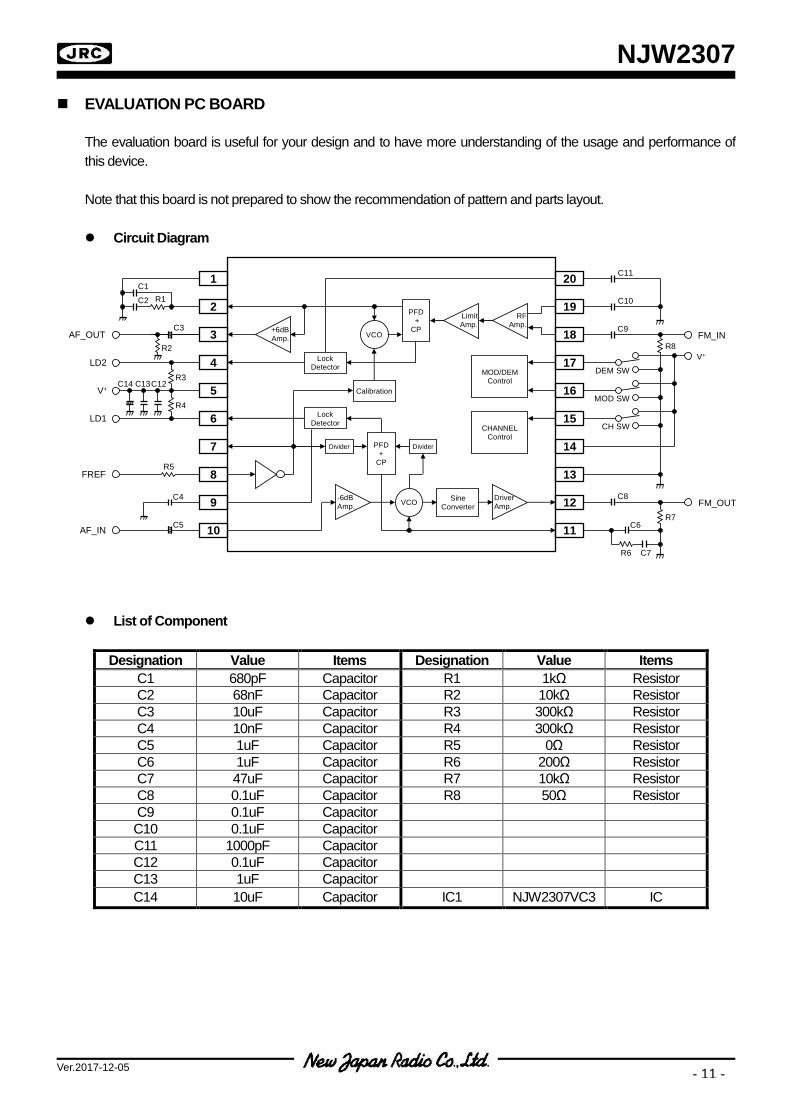
EVALUATION PC BOARD The evaluation board is useful for your design and to have more understanding of the usage and performance of this device. Note that this board is not prepared to show the recommendation of pattern and parts layout. Circuit Diagram
TYPICAL CHARACTERISTICS (Ta = 25°C, V+ = 5.0V, fref = 4.0MHz, FM IN = 1Vpp, fdev = ±15kHz, fmod = 1kHz, AF IN = 0.5Vpp, AFfreq = 1kHz, FMOUT = 10kΩ, AFOUT = 10kΩ, unless otherwise noted.)
0.0
0.2
0.4
0.6
0.8
1.0
3 4 5 6Pow
er D
own
Ope
ratin
g C
urre
ntI P
D (
uA )
Supply Voltage V+ (V)
Power Down Operating Currentvs. Supply Voltage
( Temperature Characteristic )
Ta= 85°C
-40°C 25°C
0.0
0.2
0.4
0.6
0.8
1.0
-50 0 50 100Pow
er D
own
Ope
ratin
g C
urre
ntI P
D (
uA )
Temperature Ta ( °C )
Power Down Operating Currentvs. Temperature
( Supply Voltage Characteristic )
V+= 5.5V
5.0V
3.8V
0
2
4
6
3 4 5 6B
IAS
Ter
min
al V
olta
geV
BIA
S ( V
)Supply Voltage V+ ( V )
BIAS Terminal Voltagevs. Supply Voltage ( H-Level )
Logical H area
0
2
4
6
3 4 5 6
Con
trol T
erm
inal
Vol
tage
VS
W 1
/2( V
)
Supply Voltage V+ ( V )
Control Terminal Voltagevs. Supply Voltage ( H / L -Level)
Logical L area
Logical H area
NJW2307
Ver.2017-12-05 - 14 -
10
12
14
16
18
20
22
3 4 5 6
Mod
-Dem
od O
pera
ting
Cur
rent
I MO
DE
M( m
A )
Supply Voltage V+ ( V )
Mod-Demod Operating Current vs. Supply Voltage
( Temperature Characteristic )
Ta= 25°C
-40°C 85°C
10
12
14
16
18
20
22
-50 0 50 100
Mod
-Dem
od O
pera
ting
Cur
rent
I MO
DE
M( m
A )
Temperature Ta ( °C )
Mod-Demod Operating Current vs. Temperature
( Supply Voltage Characteristic )
V+= 5.5V
5.0V
3.8V
6
8
10
12
3 4 5 6
Dem
odul
atio
n O
pera
ting
Cur
rent
I DE
MO
D( m
A )
Supply Voltage V+ ( V )
Demodulation Operating Current vs. Supply Voltage
( Temperature Characteristic )
Ta = 25°C
-40°C 85°C
6
8
10
12
-50 0 50 100
Dem
odul
atio
n O
pera
ting
Cur
rent
I DE
MO
D( m
A )
Temperature Ta ( °C )
Demodulation Operating Current vs. Temperature
( Supply Voltage Characteristic )
V+= 5.5V
5.0V
3.8V
6
8
10
12
3 4 5 6
Mod
ulat
ion
Ope
ratin
g C
urre
ntI M
OD
( mA
)
Supply Voltage V+ ( V )
Modulation Operating Current vs. Supply Voltage
( Temperature Characteristic )
-40°C 25°C
Ta= 85°C
6
8
10
12
-50 0 50 100
Mod
ulat
ion
Ope
ratin
g C
urre
ntI M
OD
( mA
)
Temperature Ta ( °C )
Modulation Operating Current vs. Temperature
( Supply Voltage Characteristic )
V+= 5.5V
5.0V
3.8V
NJW2307
Ver.2017-12-05 - 15 -
0.6
0.8
1.0
1.2
1.4
3 4 5 6
Car
rier O
utpu
t Lev
elV
FMO
UT
( V )
Supply Voltage V+ ( V )
Carrier Output Level vs. Supply Voltage
( Temperature Characteristic )
Ta= 85°C
25°C
-40°C
0
25
50
75
100
3 4 5 6
Car
rier O
utpu
tH
arm
onic
s Le
vel
PH
W1
( mV
)
Supply Voltage V+ ( V )
Carrier Output Harmonics Level vs. Supply Voltage
( Temperature Characteristic )
Ta= 85°C
-40°C 25°C
10
13
15
18
20
3 4 5 6
Mod
ulat
ion
dept
hF D
EV( ±
kHz
)
Supply Voltage V+ ( V )
Modulation depth vs. Supply Voltage
( Temperature Characteristic )
Ta= 85°C
-40°C 25°C
0.6
0.8
1.0
1.2
1.4
-50 0 50 100
Car
rier O
utpu
t Lev
elV
FMO
UT
( V )
Temperature Ta ( °C )
Carrier Output Level vs. Temperature
( Supply Voltage Characteristic )
V+= 3.8V 5.0V 5.5V
0
25
50
75
100
-50 0 50 100
Car
rier O
utpu
tH
arm
onic
s Le
vel
PH
W1
( mV
)
Temperature Ta ( °C )
Carrier Output Harmonics Level vs. Temperature
( Supply Voltage Characteristic )
V+= 3.8V 5.0V 5.5V
10
13
15
18
20
-50 0 50 100
Mod
ulat
ion
dept
hF D
EV
( ±kH
z )
Temperature Ta ( °C )
Modulation depth vs. Temperature
( Supply Voltage Characteristic )
V+= 5.5V 5.0V
3.8V
NJW2307
Ver.2017-12-05 - 16 -
0.3
0.5
0.7
0.9
-50 0 50 100
Dem
odul
atio
n Le
velV
AFO
UT
( Vpp
)
Temperature Ta ( °C )
Demodulation Level vs. Temperature
( Supply Voltage Characteristic )
V+= 3.8V
5.0V 5.5V
-15
-10
-5
0
5
0.1 1 10 100
Car
rier O
utpu
t Lev
el,D
emod
ulat
ion
Leve
l ( d
B )
Load Resistor ( kΩ )
Carrier Output Level and Demodulation Level
vs. Load Resistor
V AF OUT
V FM OUT
-2
-1
0
1
2
20 30 40 50 60 70 80
Car
rier O
utpu
t Lev
el,D
emod
ulat
ion
Leve
l ( d
B )
FREF Duty Ratio ( % )
Carrier Output Level and Demodulation Level
vs. FREF Duty Ratio
V AF OUT
F DEV
0
10
20
30
40
50
60
-50
-40
-30
-20
-10
0
10
20 40 60 80 100 120
THD
( %
)
S+N
,N (
dB )
FM Input Level ( dBuV )
Demodulation S+N,N,THDvs. FM Input Level
N
THD
S+N
0.3
0.5
0.7
0.9
3 4 5 6
Dem
odul
atio
n Le
velV
AFO
UT
( Vpp
)
Supply Voltage V+ ( V )
Demodulation Level vs. Supply Voltage
( Temperature Characteristic )
Ta= 85°C 25°C
-40°C
NJW2307
Ver.2017-12-05 - 17 -
0
5
10
15
20
100 1000 10000Mod
ulat
ion
dept
hF D
EV( ±
kHz
)
AF Input Frequency ( Hz )
Modulation depth vs. AF Input Frequency
0.0
0.2
0.4
0.6
0.8
1.0
100 1000 10000Dem
odul
atio
n Le
velV
AFO
UT
( Vpp
)Modulation Frequency fmod ( Hz )
Demodulation Level vs. Modulation Frequency
NJW2307
Ver.2017-12-05 - 18 -
Product Outline NJW2307 consists from some blocks such as a FM modulator, a FM demodulator, a reference oscillator and a parallel
logic control interface. It's possible by a logical interface that the power of the FM modulator and demodulator can be controlled independently, and setting of a carrier frequency.
1. FM Modulation Block The speech signal gets into the AF_IN terminal (pin 10) and becomes FM modulated signal at VCO of FM modulation
through a buffer amplifier (-6dB Amp). The FM modulated signal becomes a sine wave at the Sine Converter, and it is output through a driver amplifier. The FM modulator is using PLL, and consists of PFD (Phase/Frequency detector), a CP (Charge Pump), Divider and VCO. The loop filter connected to FIL2 terminal (pin 11) can establish modulation bandwidth. 2. FM Demodulation Block The FM signal fed into the FM_IN terminal (pin 18) is demodulated in the PFD (Phase/Frequency detector), passing
through the internal RF amplifier and the limiter amplifier. The FM demodulated signal outputs from a driver amplifier (+6dB Amp). The FM demodulator is using PLL, and consists of PFD (Phase/Frequency detector), a CP (Charge Pump), Divider and VCO. The loop filter connected to FIL1 terminal (pin 2) can establish demodulation bandwidth. 3. Reference Frequency Oscillator There is an internal inverter amplifier between the OSC (pin 7) and the FREF (pin 8), a resonator connection between
2 pins makes the reference oscillator of PLL. In case of using an external PLL reference frequency signal, please input it to the FREF terminal (8pin), and leave the OSC terminal (7pin) open (no connection). 4. Parallel logic control Interface The input of an interface circuit is 3 terminals such as CH_SEL terminal (pin 15), MOD_SW terminal (pin 16) and
DEM_SW terminal (pin 17). The carrier frequency of FM modulation and demodulation can be set to 2.3MHz or 2.8MHz by the CH_SEL terminal (15pin). Further, please always set the BIAS terminal (pin 14) to a logical high level. Setting of MOD_SW terminal (pin 16) can control the power-down function in the FM modulation block. Setting of DEM_SW terminal (pin 17) can control the power-down function in the FM demodulation block.
NJW2307
Ver.2017-12-05 - 19 -
Example and explanation in the FM modulation block
When MOD_SW terminal (pin 16) is set to a logical high level, the FM modulation block will be the power-on state, and a PLL works for FM modulation, and the desired carrier signal is out from FM_OUT terminal (pin 12). LD1 terminal (pin 6) will indicate the lock status of the PLL for FM modulation, and it becomes a logical low level
when the carrier frequency becomes the set frequency. The input signal of AF_IN terminal (pin 10) becomes FM modulated signal after LD1 terminal (pin 6) becomes a logical low level. The input signal of AF_IN terminal (pin 10) doesn't become FM modulated signal while LD1 terminal (pin 6) is a logical high level. Therefore it recommends inputting a signal to AF_IN terminal after LD1 terminal (6pin) will be a logical low level. But, there is no problem with inputting a signal to AF_IN terminal (pin 10), even if LD1 terminal (pin 6) is a logical high level (PLL is unlocked status) or MOD_SW terminal (pin 16) is a logical low level (in power-down state).
Power ONPLL UnLock state
Power ONPLL Lock state( FM Modulation operation )
Control waveform of MOD_SW
Input waveform of AF_IN
Output waveform of LD1
Output waveform of FM_OUT
Power Down
L
H
L
H
NJW2307
Ver.2017-12-05 - 20 -
Example and explanation in the FM demodulation block
When DEM_SW terminal (pin 17) is set to a logical high level, an FM demodulator block is the power-on state, and a PLL works for FM demodulation, and a demodulated signal is output from AF_OUT terminal (pin 3). LD2 terminal (pin 4) will indicate the lock status of the PLL for FM demodulation, and it becomes a logical low level
when the carrier frequency into the FM_IN terminal (pin 18) becomes the same frequency of the internal VCO. The input signal of FM_IN terminal (pin 18) becomes FM demodulated signal after LD2 terminal (pin 4) becomes a logical low level. If the LD2 terminal (pin 4) is a logical high level (PLL is unlocked status), a correct demodulation signal doesn't come out because of the influence of the calibration which controls VCO for demodulation, and there is a possibility that a noise of speech bandwidth is output. Therefore when an improper FM input signal (*1) keeps being input to FM_IN terminal, it is undergoing influence of the calibration which controls VCO for demodulation, so please pay attention to this matter. (*1): An improper FM input signal
(1) Different frequency from the set frequency by CH_SEL terminal (2) In case of low input level or low SN ratio
The above AF_OUT output waveform is a reference diagram, an amplitude level and a frequency will change
caused by signal condition into the FM_IN terminal (pin 18) and environment noise.
Power ONPLL Lock state( FM Demodulation operation )
Control waveform of DEM_SW
Input waveform of FM_IN
Output waveform of LD2
Output waveform of AF_OUT
L
H
L
H
Power Down
Power ONPLL UnLock state
NJW2307
Ver.2017-12-05 - 21 -
About loop filter The loop filter which is connected to FIL1 (pin 2) or FIL2 (pin 11) terminal is needed to let PLL work stably. And it's
possible to change the frequency response of the modulation factor or demodulation level respectively by constant components of the loop filter. PLL works stably with phase margin which is generally setting of the constant component of the loop filter as more than 45 deg. When it's lacking in phase margin, the unusual situations occur, such as the PLL doesn't lock, PLL takes time to lock, or the output signal is unstable. Therefore please design the loop filter constant component to get the desired characteristics with having reserved enough phase margins. The following is the loop filter design method connected to FIL1 (pin 2) or FIL2 (pin 11) terminal of the NJW2307.
And we have an excel sheet to easily calculate the following formula, so please contact us. Design method of loop filter
The following is the way to calculate the loop filter constant component value from the condition of the cutoff
frequency cf (the frequency by which open-loop gain will be 0dB) and the phase margin c . And it shows that how
to confirm the frequency characteristic with calculated component value.
RTTC 2
11
RTC 2
2
3121
22
TTTTT
R
Time constant of a filter such as 1T , 2T and 3T are computable by the following formula under condition of
pv KKK and cc f 2 .
32
21 1
1Tj
TjNKT
cc
c
290
tan12
c
c
T
2231T
Tc
Each parameter is the following table. cf and c are given, the above calculation is performed and the loop filter
1T , 2T and 3T are regarded as the following formulas with component parameters obtained of loop filter.
211 CCT
22 RCT
21
213 CC
CRCT
About each transfer function, their frequency characteristics are computable under condition of js .
Open loop transfer function sGopen
1
231
32
NTsTNTsKsKTsGopen
Phase shift characteristic
The imaginal part of sGopen is defined as sGopenIm , and the real part of sGopen is defined as sGopenRe .
sGsG
open
open
ReIm
tan180 1
Modulation transfer function sGmod
KsKTNTsTNTs
NTsTNTssG
212
313
12
313
mod
Demodulation transfer function sGdemod
KsKTNTsTNTs
KNsKNTsGde
21
231
32
mod
Loop filter must be designed to work stably in a desired frequency response from the above calculation.
NJW2307
Ver.2017-12-05 - 23 -
Calculation example of loop filter
The following is the constant parameters and frequency characteristic as result of above calculation. The phase margin is 45 deg as the condition. S/N and harmonic distortion characteristics, etc. are strongly related to bandwidth.
Modulation depth of AF input frequency (at carrier frequency 2.8MHz)
[CAUTION] The specifications on this databook are only
given for information , without any guarantee as regards either mistakes or omissions. The application circuits in this databook are described only to show representative usages of the product and not intended for the guarantee or permission of any right including the industrial rights.