All rights strictly reserved. Reproduction or issue to third parties in any form is not permitted without written authority from Power-One. Title Issued 2006-05-05 SKl Modified 2007-07-03 SKl Mech. Eng. approved -- -- Marketing approved 2007-07-03 J. Carroll FNP1500/1800 I 2 C Interface Programming Manual Mfg. approved -- Size Scale Sheet Drawing No. Revision www.power-one.com A4 1/35 BCA20003-G AA Supersedes: - FNP1500/1800 I 2 C Interface Programming Manual 1 Scope This document describes in detail the I 2 C communication interface of the FNP1500/1800 series. (FNP1500-XX, FNP1800-XX, FXP1500-XX, FXP1800-XX) This includes the physical layer and the SW protocol. 2 FNP1500/1800 I 2 C Interface General Characteristic FNP1500/1800 I 2 C interface slave I 2 C Device Addressing Format 7bit Device Address Range 80 Hex ..BF Hex Max. FNP1500/1800 on one I 2 C Bus 32 Maximum I 2 C clock 100kHz Maximum I 2 C clock without holding the SCL line down 1.5kHz Pull-Up Voltage 3.3…5V SDA/SCL internal series resistors 0Ω Internal Pull-Up -- Internal Pull-Up voltage -- Internal capacitance 15pF Internal Pull-Up Address lines 10kΩ Internal Pull-Up Address lines voltage 5V Recommended external Pull-Up for SDA and SCL 2.2kΩ …5kΩ Data Organization Serial EEPROM (256 x 8bit) Figure 2-1 Characteristic
Transcript
All rights strictly reserved. Reproduction or issue to third parties in any form is not permitted without written authority from Power-One.
Title Issued 2006-05-05 SKl Modified 2007-07-03 SKl Mech. Eng. approved -- -- Marketing approved 2007-07-03 J. Carroll
This document describes in detail the I2C communication interface of the FNP1500/1800 series. (FNP1500-XX, FNP1800-XX, FXP1500-XX, FXP1800-XX) This includes the physical layer and the SW protocol.
2 FNP1500/1800 I2C Interface General Characteristic
FNP1500/1800 I2C interface slave I2C Device Addressing Format 7bit Device Address Range 80Hex ..BFHex Max. FNP1500/1800 on one I2C Bus 32 Maximum I2C clock 100kHz Maximum I2C clock without holding the SCL line down 1.5kHz Pull-Up Voltage 3.3…5V SDA/SCL internal series resistors 0Ω Internal Pull-Up -- Internal Pull-Up voltage -- Internal capacitance 15pF Internal Pull-Up Address lines 10kΩ Internal Pull-Up Address lines voltage 5V Recommended external Pull-Up for SDA and SCL 2.2kΩ …5kΩ Data Organization Serial EEPROM (256 x 8bit)
1 Scope......................................................................................................................................................1 2 FNP1500/1800 I2C Interface General Characteristic.............................................................................1 3 Index ......................................................................................................................................................2 4 FNP1500/1800 I2C Features .................................................................................................................3
4.1 Dynamic data .................................................................................................................................3 4.2 Static data.......................................................................................................................................3
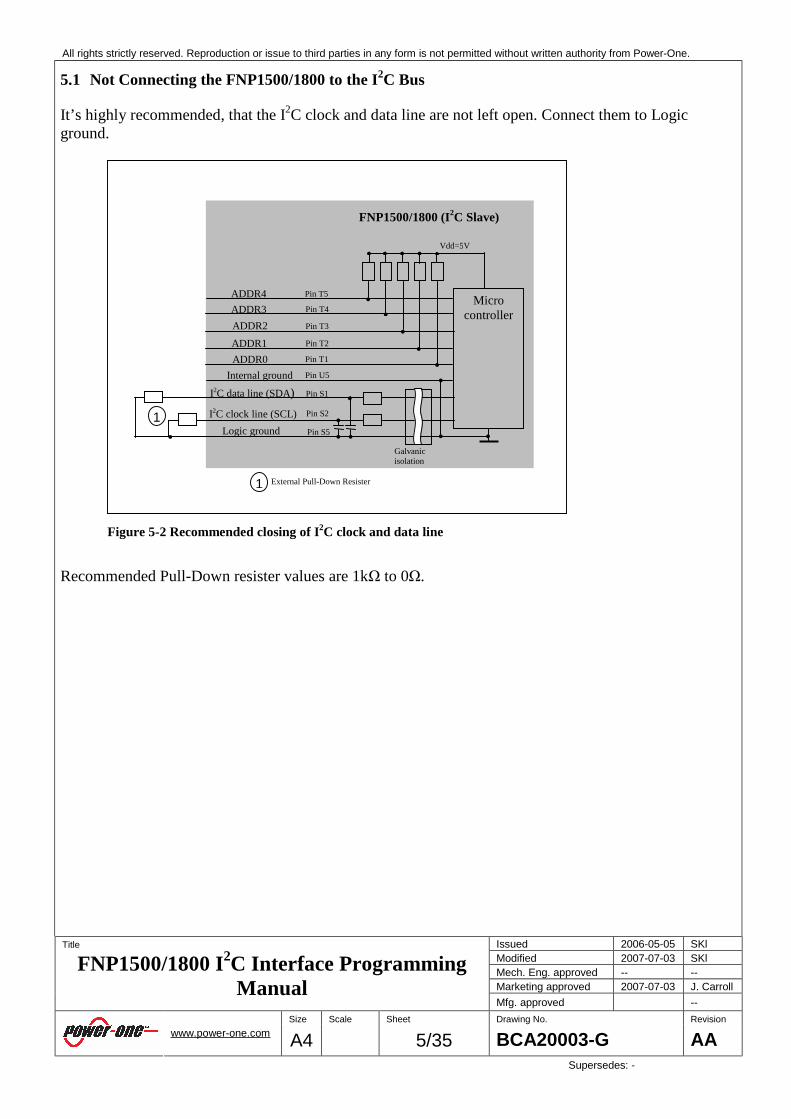
5 General I2C HW configuration ..............................................................................................................4 5.1 Not Connecting the FNP1500/1800 to the I2C Bus .......................................................................5 5.2 Connecting the FNP1500/1800 to the I2C Bus ..............................................................................6 5.3 FNP1500/1800 I2C Supply (Slave)................................................................................................7 5.4 Device Address ..............................................................................................................................7 5.5 I2C Bus Master and clock (SCL) speed .........................................................................................9 5.6 Maximum and minimum values for Pull-Up resisters...................................................................9
6 SW Protocol.........................................................................................................................................10 6.1 How to Read a byte......................................................................................................................11 6.2 How to write a Byte .....................................................................................................................12 6.3 Error Handling .............................................................................................................................13
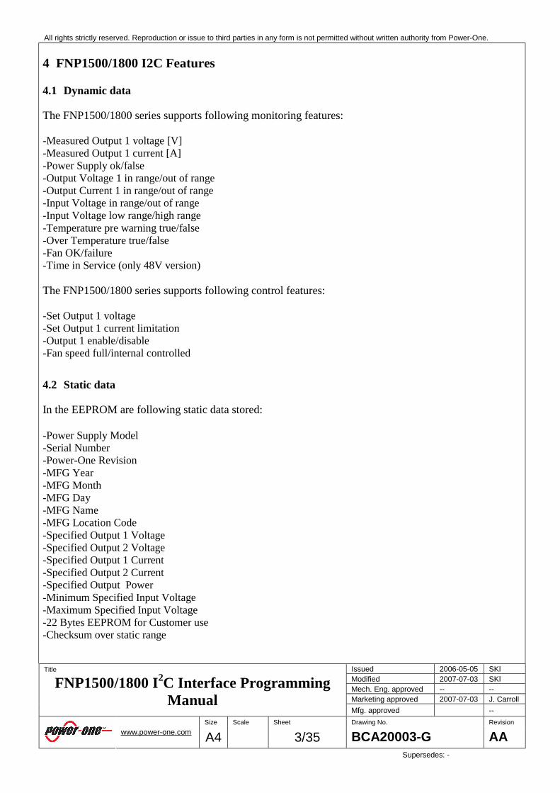
The FNP1500/1800 series supports following monitoring features: -Measured Output 1 voltage [V] -Measured Output 1 current [A] -Power Supply ok/false -Output Voltage 1 in range/out of range -Output Current 1 in range/out of range -Input Voltage in range/out of range -Input Voltage low range/high range -Temperature pre warning true/false -Over Temperature true/false -Fan OK/failure -Time in Service (only 48V version) The FNP1500/1800 series supports following control features: -Set Output 1 voltage -Set Output 1 current limitation -Output 1 enable/disable -Fan speed full/internal controlled
4.2 Static data
In the EEPROM are following static data stored: -Power Supply Model -Serial Number -Power-One Revision -MFG Year -MFG Month -MFG Day -MFG Name -MFG Location Code -Specified Output 1 Voltage -Specified Output 2 Voltage -Specified Output 1 Current -Specified Output 2 Current -Specified Output Power -Minimum Specified Input Voltage -Maximum Specified Input Voltage -22 Bytes EEPROM for Customer use -Checksum over static range
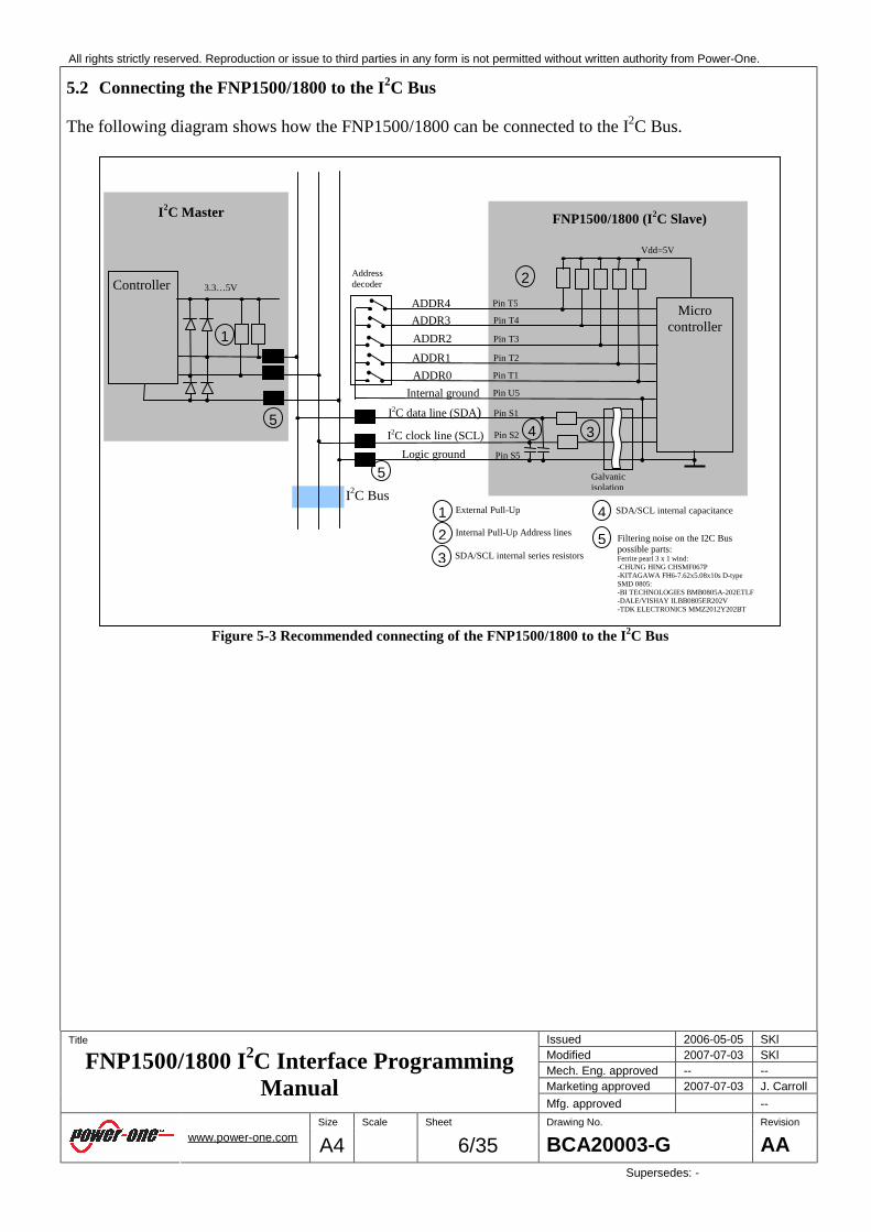
To not exceed the I2C Bus limits of 400pF on the Bus, it’s recommended to use an I2C Bus repeater (like PCA9515 from Philips or Texas Instruments) for more than five FNP1500/1800 units.
The following diagram shows how the FNP1500/1800 can be connected to the I2C Bus.
Figure 5-3 Recommended connecting of the FNP1500/1800 to the I2C Bus
Micro controller
ADDR2 ADDR3
Pin T3
Pin T4
Vdd=5V
::
:
ADDR1 Pin T2 :
FNP1500/1800 (I2C Slave)
:
I2C data line (SDA) I2C clock line (SCL)
Pin S1
Pin S2
Pin S5 Logic ground
:::::::: :
Address decoder 3.3…5V
::
:
::
:
I2C Master
I2C Bus
1
3
2
1 External Pull-Up
2 Internal Pull-Up Address lines
3 SDA/SCL internal series resistors
:::
ADDR0
ADDR4 Pin T5
Pin T1
:
:
:: :
:::
:Galvanic isolation
Internal ground Pin U5
::4
:
:: :
4 SDA/SCL internal capacitance
::
::
::
: :
::
5
5
5
Filtering noise on the I2C Bus possible parts: Ferrite pearl 3 x 1 wind: -CHUNG HING CHSMF067P -KITAGAWA FH6-7.62x5.08x10s D-type SMD 0805: -BI TECHNOLOGIES BMB0805A-202ETLF -DALE/VISHAY ILBB0805ER202V -TDK ELECTRONICS MMZ2012Y202BT
The FNP1500/1800 Micro Controller is powered over the internal supply of the FNP1500. In case of AC failure or FNP1500/1800 internal failure there is no power for the FNP1500/1800 Micro Controller. This will have no influence on the I2C Bus, but the FNP1500/1800 Micro Controller will not respond to the I2C Master.
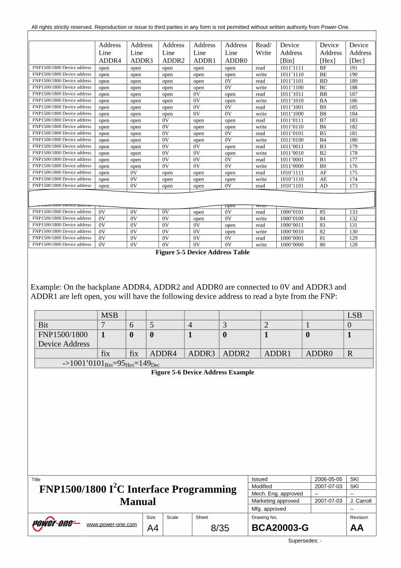
5.4 Device Address
The first byte after the START condition on the Bus is the device address sent out by the Bus Master to determine which device is being selected. The I2C Bus allows 7-bit or 10-bit addressing. The FNP1500/1800 Interface uses a 7-bit address mode as defined in the Philips I²C specification. Each FNP1500/1800 device has to be assigned to a unique address. As shown below in Figure 5-4 Device Address the address byte is built up from three parts: - Bit 6, 7: These bits are always the same independent of any address line. - Bit 1...5: These bits depends how the Address line A0...A4 is connected on the backplane on the address
decoder. These are logic 1 if open and logic 0 if wired to 0V (12V Standby RTN). -Bit 0: This bit is the read/write bit (R=1/W=0) and determines the direction of the data from or to the Master.
FNP1500/1800 Device Address
Device Hardware Address Software Address Bit
MSB LSB Bit 7 6 5 4 3 2 1 0 Determined via Fixed Per
FNP1500/1800 Device address open open open open open read 1011’1111 BF 191 FNP1500/1800 Device address open open open open open write 1011’1110 BE 190 FNP1500/1800 Device address open open open open 0V read 1011’1101 BD 189 FNP1500/1800 Device address open open open open 0V write 1011’1100 BC 188 FNP1500/1800 Device address open open open 0V open read 1011’1011 BB 187 FNP1500/1800 Device address open open open 0V open write 1011’1010 BA 186 FNP1500/1800 Device address open open open 0V 0V read 1011’1001 B9 185 FNP1500/1800 Device address open open open 0V 0V write 1011’1000 B8 184 FNP1500/1800 Device address open open 0V open open read 1011’0111 B7 183 FNP1500/1800 Device address open open 0V open open write 1011’0110 B6 182 FNP1500/1800 Device address open open 0V open 0V read 1011’0101 B5 181 FNP1500/1800 Device address open open 0V open 0V write 1011’0100 B4 180 FNP1500/1800 Device address open open 0V 0V open read 1011’0011 B3 179 FNP1500/1800 Device address open open 0V 0V open write 1011’0010 B2 178 FNP1500/1800 Device address open open 0V 0V 0V read 1011’0001 B1 177 FNP1500/1800 Device address open open 0V 0V 0V write 1011’0000 B0 176 FNP1500/1800 Device address open 0V open open open read 1010’1111 AF 175 FNP1500/1800 Device address open 0V open open open write 1010’1110 AE 174 FNP1500/1800 Device address open 0V open open 0V read 1010’1101 AD 173 FNP1500/1800 Device address 0V 0V 0V open open read 1000’0111 87 135 FNP1500/1800 Device address 0V 0V 0V open open write 1000’0110 86 134 FNP1500/1800 Device address 0V 0V 0V open 0V read 1000’0101 85 133 FNP1500/1800 Device address 0V 0V 0V open 0V write 1000’0100 84 132 FNP1500/1800 Device address 0V 0V 0V 0V open read 1000’0011 83 131 FNP1500/1800 Device address 0V 0V 0V 0V open write 1000’0010 82 130 FNP1500/1800 Device address 0V 0V 0V 0V 0V read 1000’0001 81 129 FNP1500/1800 Device address 0V 0V 0V 0V 0V write 1000’0000 80 128
Figure 5-5 Device Address Table Example: On the backplane ADDR4, ADDR2 and ADDR0 are connected to 0V and ADDR3 and ADDR1 are left open, you will have the following device address to read a byte from the FNP:
The I2C Bus Master controls communications between the Master and all I2C devices connected to the bus. If during an I2C communication cycle the FNP1500/1800 is interrupted by an internal service interrupt, the FNP1500/1800 will hold the SCL line low to force the master into a wait state. Data transfer will continue when the FNP1500/1800 releases the SCL line. Please note if the I2C bus is communicating with a clock frequency slower than 1.5kHz, the SCL line will not be held low.
5.6 Maximum and minimum values for Pull-Up resisters
For I2C-bus systems, the values of the Pull-Up resistors depend on the following parameters: • Supply voltage • Bus capacitance • Number of connected devices (input current + leakage current). The supply voltage limits the minimum value of the Pull-Up resistor due to the specified minimum sink current of 3mA. On a 5V supply, this makes Rmin=5V/3mA=1.7kΩ. The bus capacitance is the total capacitance of wire, connections and pins. This capacitance limits the maximum value of the Pull-Up resister due to the specified rise time. For a System with 150pF capacitance (three FNP1500/1800 at 15pF and a wire capacitance of 105pF) Rmax=5kΩ. For further information concerning the Pull-Up resister, refer to: I²C Bus specification, 16.1 Maximum and minimum values of resistors Rp and Rs for Standard-mode I2C-bus devices.
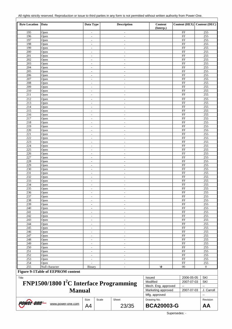
The data are organized like a serial I2C EEPROM. Therefore each EEPROM address has defined data; this definition is documented in the chapter 9 EEPROM Table.
Dec Hex Address 0 static data 0
1 static data 1
79 static data 4F 80 static data 50 81 open for customer use 51 82 open for customer use 52
102 open for customer use 66 103 checksum over range above 67 104 reserved 68 105 reserved 69
127 reserved 7F 128 dynamic data 80 129 dynamic data 81
186 dynamic data BA 187 reserved BB 188 reserved BC
255 reserved FF
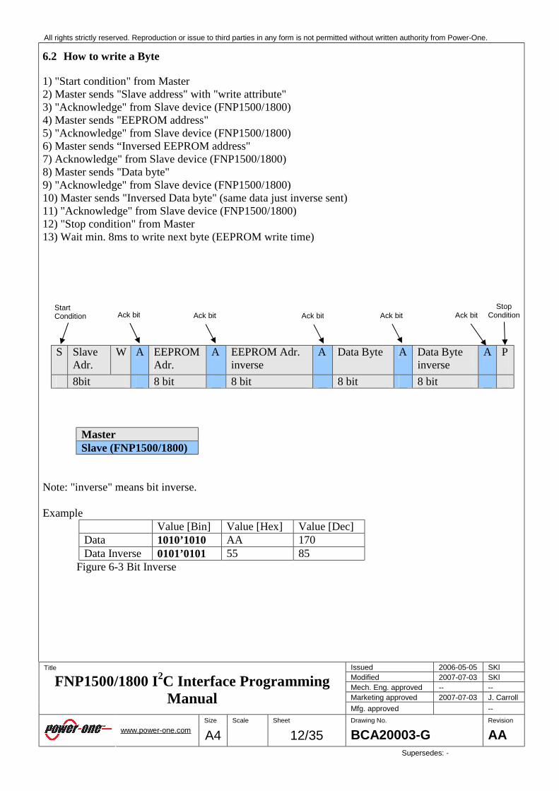
Figure 6-1 Data Organization There are three different message formats implemented in the FNP1500/1800: -Read a byte -Write a byte
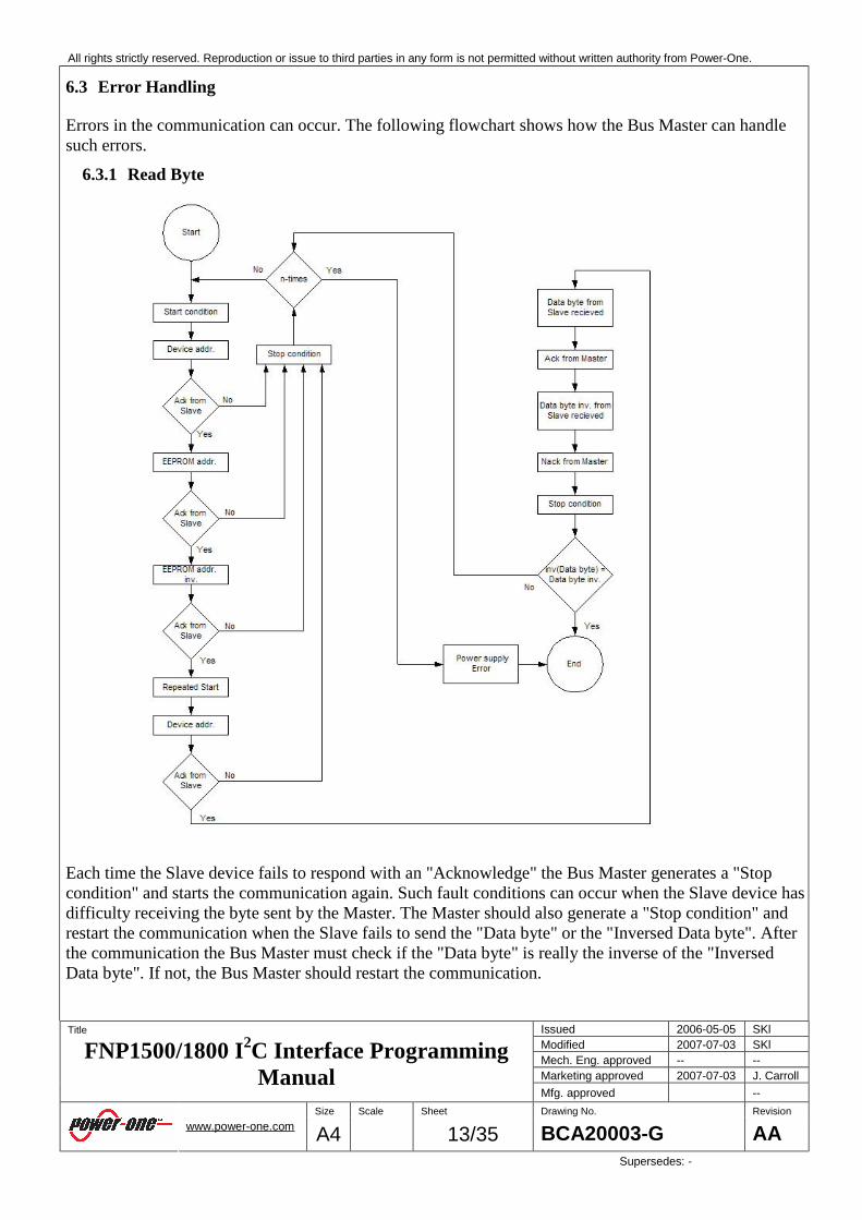
Errors in the communication can occur. The following flowchart shows how the Bus Master can handle such errors.
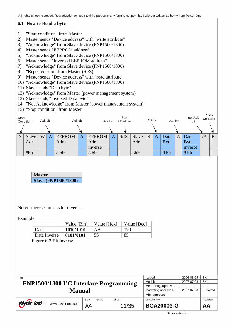
6.3.1 Read Byte
Each time the Slave device fails to respond with an "Acknowledge" the Bus Master generates a "Stop condition" and starts the communication again. Such fault conditions can occur when the Slave device has difficulty receiving the byte sent by the Master. The Master should also generate a "Stop condition" and restart the communication when the Slave fails to send the "Data byte" or the "Inversed Data byte". After the communication the Bus Master must check if the "Data byte" is really the inverse of the "Inversed Data byte". If not, the Bus Master should restart the communication.
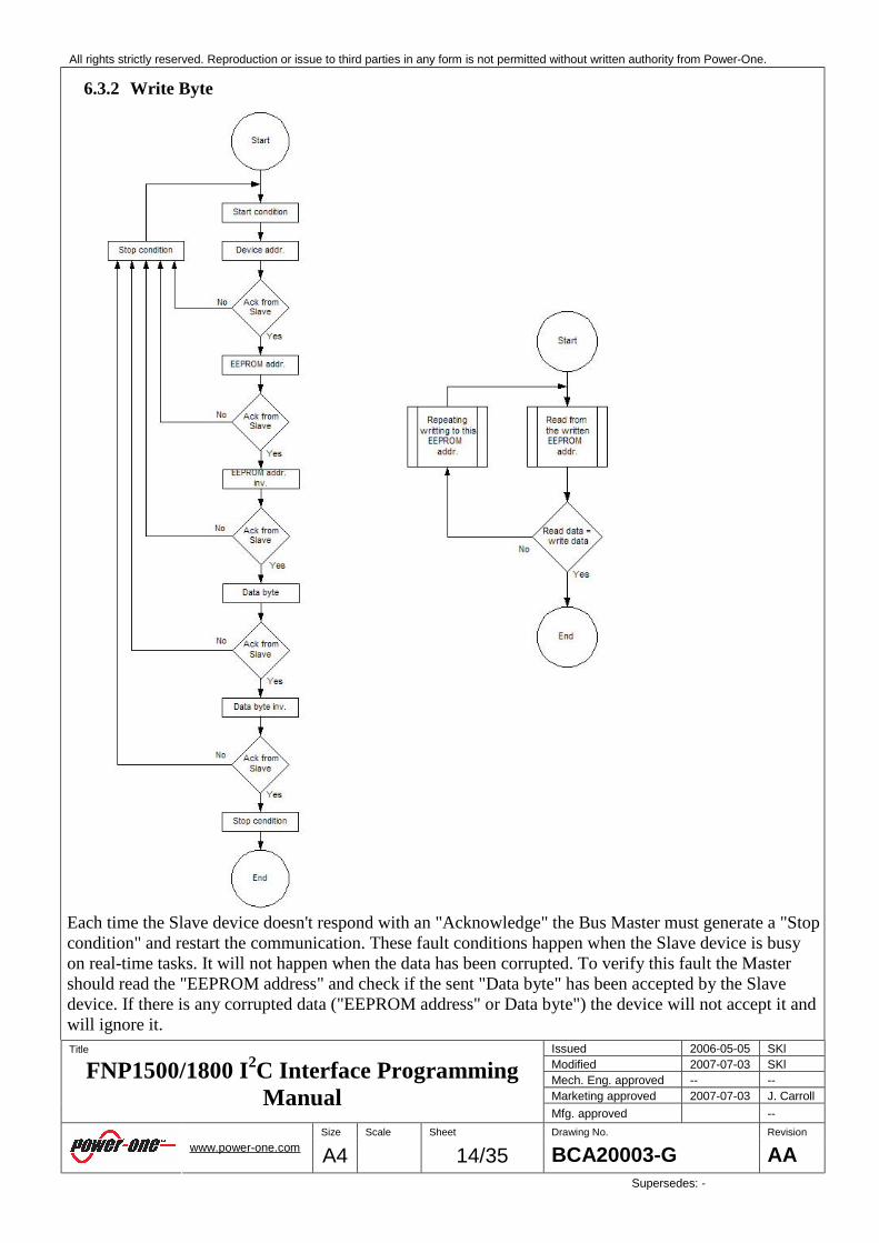
Each time the Slave device doesn't respond with an "Acknowledge" the Bus Master must generate a "Stop condition" and restart the communication. These fault conditions happen when the Slave device is busy on real-time tasks. It will not happen when the data has been corrupted. To verify this fault the Master should read the "EEPROM address" and check if the sent "Data byte" has been accepted by the Slave device. If there is any corrupted data ("EEPROM address" or Data byte") the device will not accept it and will ignore it.
Figure 8-2 HZZ02002G to FNP1500/1800 setup Plug one or more FNP1500/1800 into the power shelf connect the HZZ02002G to the power shelf and power up the FNP1500/1800. Power Shelf Number to the according FNP1500/1800 Model:
FNP1500/1800 Model Power Shelf Number FNP1500-48 FNR-3-48G FNP1800-48 FNR-3-48G FXP1500-48 FXR-3-48G FXP1800-48 FXR-3-48G FNP1500-12 FNR-3-12G
Figure 8-3 Power Shelf Number to the according FNP1500/1800 Model The I2C device address will be according the Dip-Switch on the Power Shelf, the I2C address will be found automatic by the Software. (HZZ02002SW). In your final application the I2C master will be a Micro Computer or an FPGA with an I2C interface. That makes it easy and inexpensive to use the interface.
Blue marked cells, are example data for the FNP1500-48 model. Byte Location Data Data
Type Description Content
(Interp.) Content (HEX)
Content (DEC)
0 Number of Char. NUM Num. of characters in Model Num
10 0A
10
1 Power-One part nr. ASCII Supply Model Num. F 46 70 2 Power-One part nr. ASCII N 4E 78 3 Power-One part nr. ASCII P 50 80 4 Power-One part nr. ASCII 1 31 49 5 Power-One part nr. ASCII 5 35 53 6 Power-One part nr. ASCII 0 30 48 7 Power-One part nr. ASCII 0 30 48 8 Power-One part nr. ASCII - 2D 45 9 Power-One part nr. ASCII 4 34 52
10 Power-One part nr. ASCII 8 38 56 11 Power-One part nr. ASCII FF 255 12 Power-One part nr. ASCII FF 255 13 Power-One part nr. ASCII FF 255 14 Power-One part nr. ASCII FF 255 15 Power-One part nr. ASCII FF 255 16 Power-One part nr. ASCII FF 255 17 Power-One part nr. ASCII
See Annex A
FF 255
18 Number of Char. NUM Num. of characters in Serial Num
11 0B 11
19 Serial Number ASCII Serial number xx xx xx 20 Serial Number ASCII xx xx xx 21 Serial Number ASCII xx xx xx 22 Serial Number ASCII xx xx xx 23 Serial Number ASCII xx xx xx 24 Serial Number ASCII xx xx xx 25 Serial Number ASCII xx xx xx 26 Serial Number ASCII xx xx xx 27 Serial Number ASCII xx xx xx 28 Serial Number ASCII xx xx xx 29 Serial Number ASCII xx xx xx 30 Serial Number ASCII FF 255
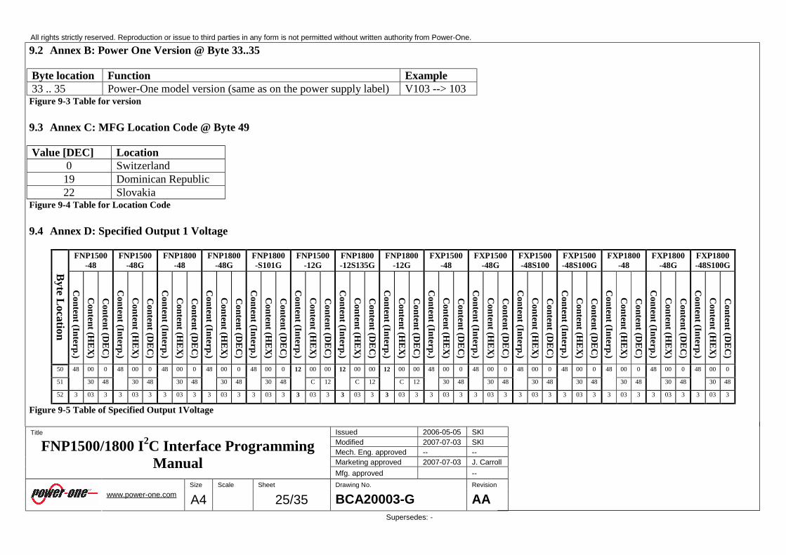
31 Number of Char. NUM Num. of characters in Version 4 04 4 32 Version Level ASCII Power-One Version 0 30 48 33 Version Level ASCII xx xx xx 34 Version Level ASCII xx xx xx 35 Version Level ASCII
See Annex
B xx xx xx
36 MFG Year NUM (000-255) xx xx xx 37 MFG Month NUM 1-12 xx xx xx 38 MFG Day NUM 1-31 xx xx xx
39 Number of Char. NUM Num. of characters in MFG Name
9 09 9
40 MFG Name ASCII Power-One P 50 80 41 MFG Name ASCII O 4F 79 42 MFG Name ASCII W 57 87 43 MFG Name ASCII E 45 69 44 MFG Name ASCII R 52 82 45 MFG Name ASCII - 2D 45 46 MFG Name ASCII O 4F 79 47 MFG Name ASCII N 4E 78 48 MFG Name ASCII E 45 69 49 MFG Location Code HEX Power One Mfg Location Code See
Annex C
xx xx xx
50 00 0 51
Output 1 Voltage
NUM
48 30 48
52 Output 1 Voltage Scale NUM
Specified Output 1 Voltage 2 Byte number / (10^Scale)
(In milliVolts)
See Annex D
3 03 3 53 00 0 54
Output 2 Voltage
NUM
12 0C 12
55 Output 2 Voltage Scale NUM
Specified Output 2 Voltage 2 Byte number / (10^Scale)
(In milliVolts)
See Annex E
3 03 3
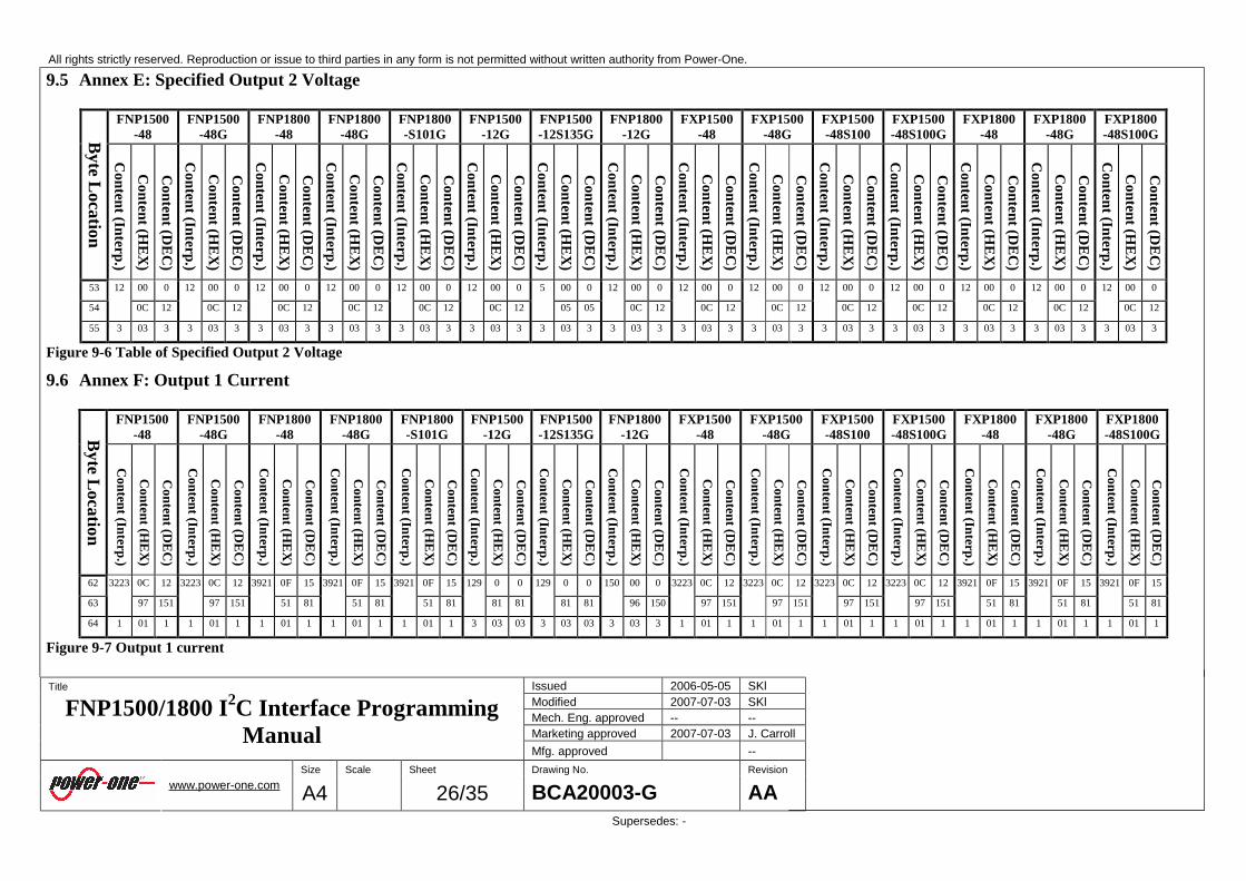
56 FF 255 57
- - FF 255
58 - -
-
FF 255 59 FF 255 60
- - FF 255
61 - -
-
FF 255 62 0C 12 63
Output 1 Current
NUM NUM
3223 97 151
64 Output 1 Current Scale NUM
Specified Output 1 Current 2 Byte number / (10^Scale)
(In milliAmps)
See Annex
F 1 01 1
65 00 0 66
Output 2 Current
NUM
1 01 1
67 Output 2 Current Scale NUM
Specified Output 2 Current 2 Byte number / (10^Scale)
80 Number of Char. NUM Num. of characters in Customer Specific
22 16 22
81 Customer Specific Data - - 00 0 82 Customer Specific Data - - 00 0 83 Customer Specific Data - - 00 0 84 Customer Specific Data - - 00 0 85 Customer Specific Data - - 00 0 86 Customer Specific Data - - 00 0 87 Customer Specific Data - - 00 0 88 Customer Specific Data - - 00 0 89 Customer Specific Data - - 00 0 90 Customer Specific Data - - 00 0 91 Customer Specific Data - - 00 0 92 Customer Specific Data - - 00 0 93 Customer Specific Data - - 00 0 94 Customer Specific Data - - 00 0 95 Customer Specific Data - - 00 0 96 Customer Specific Data - - 00 0 97 Customer Specific Data - - 00 0 98 Customer Specific Data - - 00 0 99 Customer Specific Data - - 00 0
100 Customer Specific Data - - 00 0 101 Customer Specific Data - - 00 0 102 Customer Specific Data - - 00 0 103 Checksum Byte Binary LSByte[Sum of static byte above] xxxxxxxx xx xx 104 Open - - FF 255 105 Open - - FF 255 106 Open - - FF 255 107 Open - - FF 255 108 Open - - FF 255 109 Open - - FF 255 110 Open - - FF 255 111 Open - - FF 255 112 Open - - FF 255 113 Open - - FF 255 114 Open - - FF 255 115 Open - - FF 255 116 Open - - FF 255 117 Open - - FF 255 118 Open - - FF 255 119 Open - - FF 255 120 Open - - FF 255 121 Open - - FF 255 122 Open - - FF 255 123 Open - - FF 255 124 Open - - FF 255 125 Open - - FF 255 126 Open - - FF 255 127 Null character Binary - \0 00 0
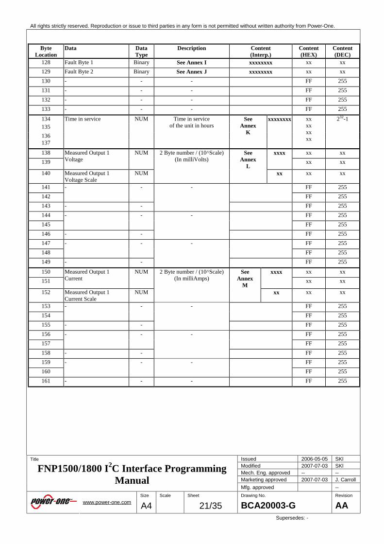
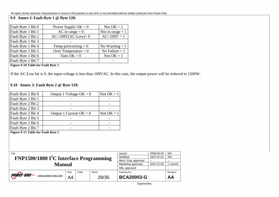
Fault Byte 1 Bit 0 Power Supply OK = 0 Not OK = 1 Fault Byte 1 Bit 1 AC in range = 0 Not in range = 1 Fault Byte 1 Bit 2 AC<108V(AC-Low)= 0 AC>108V = 1 Fault Byte 1 Bit 3 - - Fault Byte 1 Bit 4 Temp-prewarning = 0 No Warning = 1 Fault Byte 1 Bit 5 Over Temperature = 0 No Failure = 1 Fault Byte 1 Bit 6 Fans OK = 0 Not OK = 1 Fault Byte 1 Bit 7 - - Figure 9-10 Table for Fault Byte 1 If the AC-Low bit is 0, the input voltage is less than 108VAC. In this case, the output power will be reduced to 1200W.
9.10 Annex J: Fault Byte 2 @ Byte 129:
Fault Byte 2 Bit 0 Output 1 Voltage OK = 0 Not OK = 1 Fault Byte 2 Bit 1 - - Fault Byte 2 Bit 2 - - Fault Byte 2 Bit 3 - - Fault Byte 2 Bit 4 Output 1 Current OK = 0 Not OK = 1 Fault Byte 2 Bit 5 - - Fault Byte 2 Bit 6 - - Fault Byte 2 Bit 7 - - Figure 9-11 Table for Fault Byte 2
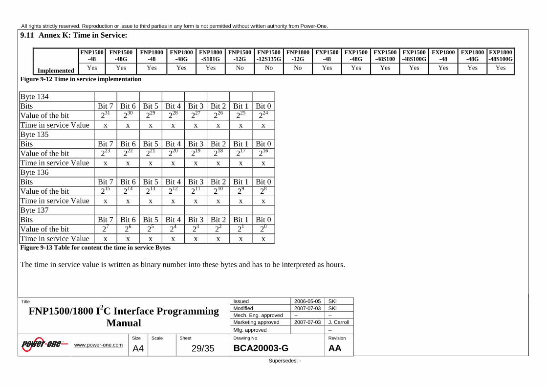
Implemented Yes Yes Yes Yes Yes No No No Yes Yes Yes Yes Yes Yes Yes
Figure 9-12 Time in service implementation Byte 134 Bits Bit 7 Bit 6 Bit 5 Bit 4 Bit 3 Bit 2 Bit 1 Bit 0 Value of the bit 231 230 229 228 227 226 225 224 Time in service Value x x x x x x x x Byte 135 Bits Bit 7 Bit 6 Bit 5 Bit 4 Bit 3 Bit 2 Bit 1 Bit 0 Value of the bit 223 222 221 220 219 218 217 216 Time in service Value x x x x x x x x Byte 136 Bits Bit 7 Bit 6 Bit 5 Bit 4 Bit 3 Bit 2 Bit 1 Bit 0 Value of the bit 215 214 213 212 211 210 29 28 Time in service Value x x x x x x x x Byte 137 Bits Bit 7 Bit 6 Bit 5 Bit 4 Bit 3 Bit 2 Bit 1 Bit 0 Value of the bit 27 26 25 24 23 22 21 20 Time in service Value x x x x x x x x Figure 9-13 Table for content the time in service Bytes The time in service value is written as binary number into these bytes and has to be interpreted as hours.
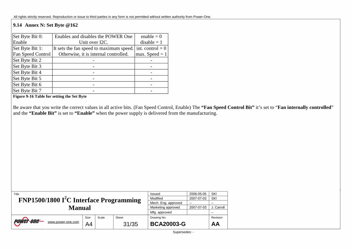
It sets the fan speed to maximum speed. Otherwise, it is internal controlled.
int. control = 0 max. Speed = 1
Set Byte Bit 2 - - Set Byte Bit 3 - - Set Byte Bit 4 - - Set Byte Bit 5 - - Set Byte Bit 6 - - Set Byte Bit 7 - - Figure 9-16 Table for setting the Set Byte Be aware that you write the correct values in all active bits. (Fan Speed Control, Enable) The “Fan Speed Control Bit” it’s set to “Fan internally controlled” and the “Enable Bit” is set to “Enable” when the power supply is delivered from the manufacturing.
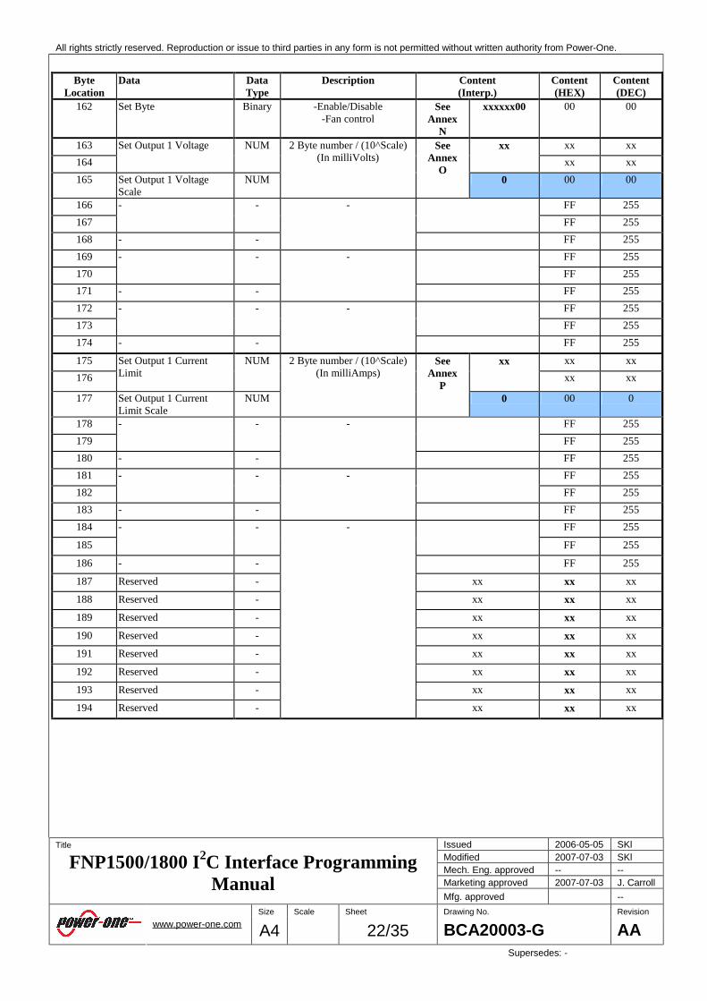
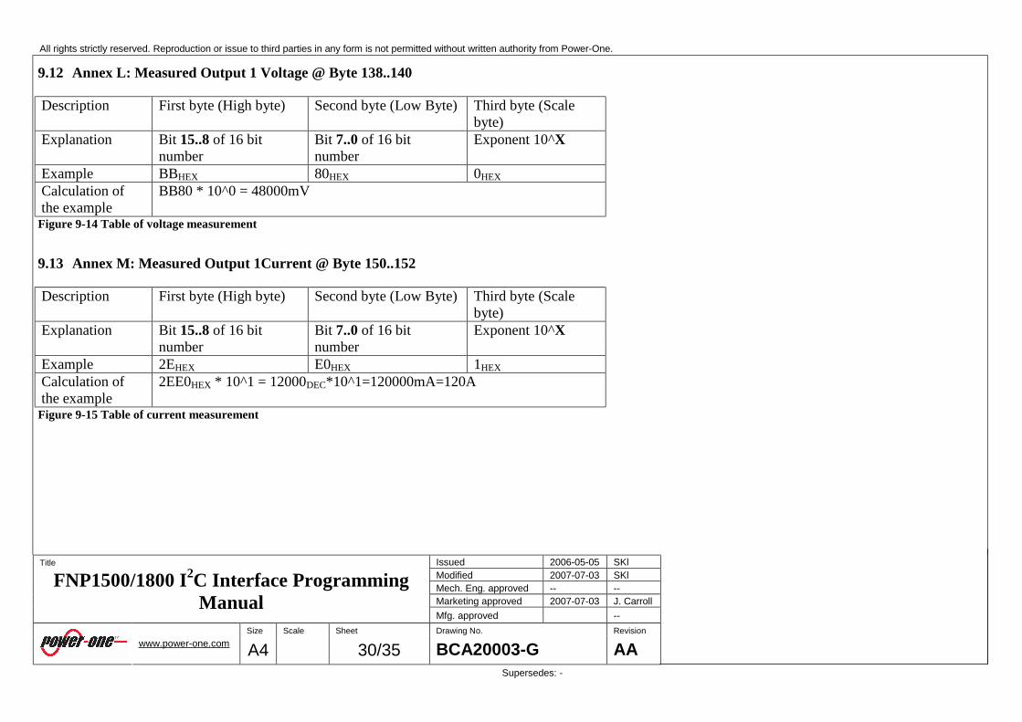
9.15 Annex O: Set Output 1 Voltage @ Byte 163..165 /
Description First byte (High byte) Second byte (Low Byte) Third byte (Scale byte) Explanation Bit 15..8 of
16 bit number Bit 7..0 of 16 bit number
Exponent 10^X
Example BBHEX 80HEX 0HEX Calculation of the example
BB80HEX * 10^0 *mV=48000DEC*10^0*mV= 48000mV
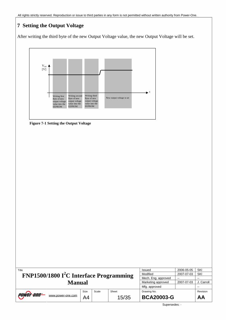
Figure 9-17 Table for setting the Set Output 1 Voltage It is necessary to rewrite all three “Set output 1 voltage bytes” (163..165) for a new setting of the output voltage. The third byte (Scale Byte) has although to be set, according to Scale Set Table below. A power supply model accepts only one scale value.
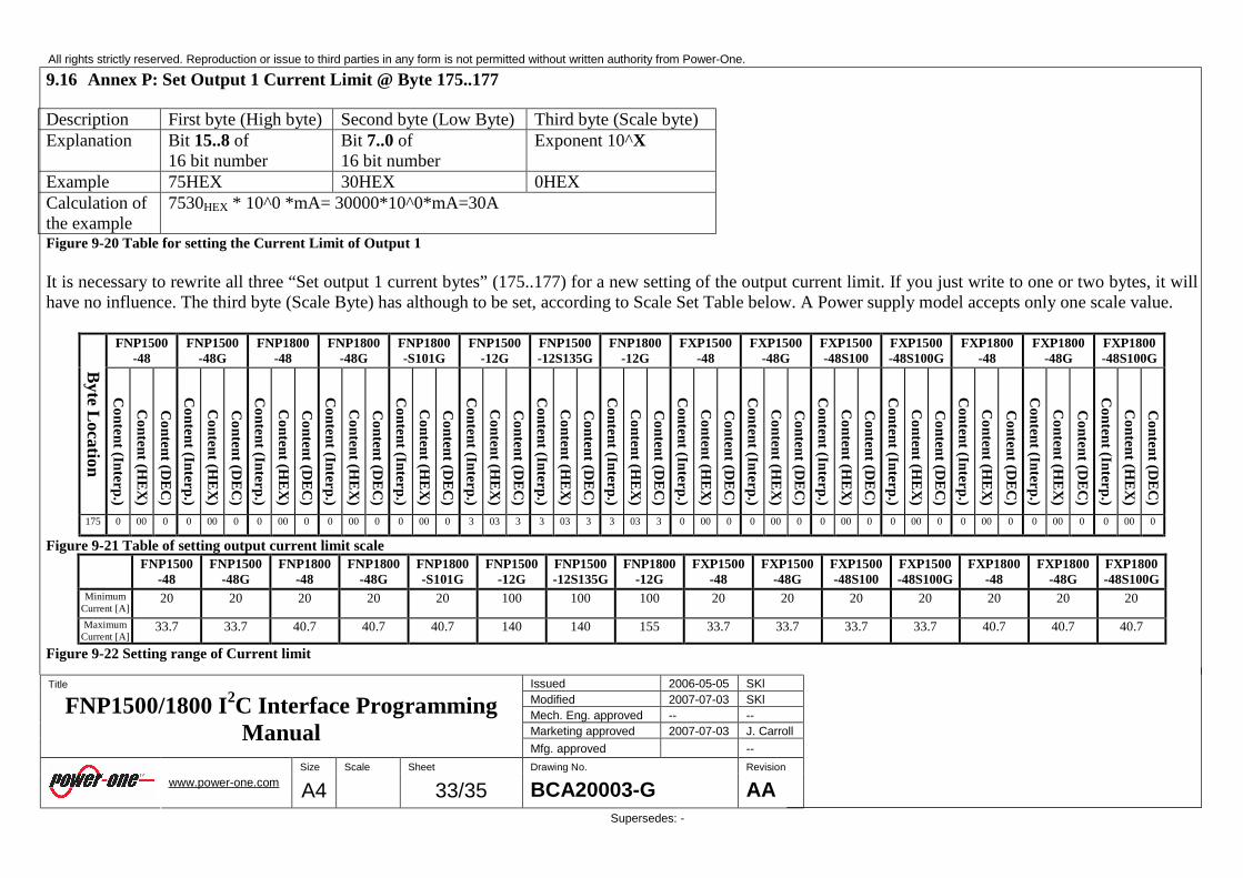
9.16 Annex P: Set Output 1 Current Limit @ Byte 175..177
Description First byte (High byte) Second byte (Low Byte) Third byte (Scale byte) Explanation Bit 15..8 of
16 bit number Bit 7..0 of 16 bit number
Exponent 10^X
Example 75HEX 30HEX 0HEX Calculation of the example
7530HEX * 10^0 *mA= 30000*10^0*mA=30A
Figure 9-20 Table for setting the Current Limit of Output 1 It is necessary to rewrite all three “Set output 1 current bytes” (175..177) for a new setting of the output current limit. If you just write to one or two bytes, it will have no influence. The third byte (Scale Byte) has although to be set, according to Scale Set Table below. A Power supply model accepts only one scale value.
-Philips Semiconductors, The I 2C-BUS Specification, V.2.1, Document order number: 9398 393 40011 http://www.nxp.com/acrobat_download/literature/9398/39340011.pdf -Philips SemiconductorsI2C Handbook http://www.nxp.com/acrobat_download/various/philips_i2c_handbook.pdf -Power-One, FNP1500/1800 and FXP1500/1800 Front-Ends & FNR-3 and FXR-3 Power Shelves Data Sheet
11 Figure Index
Figure 2-1 Characteristic ...............................................................................................................................1 Figure 5-1 System Overview .........................................................................................................................4 Figure 5-2 Recommended closing of I2C clock and data line.......................................................................5 Figure 5-3 Recommended connecting of the FNP1500/1800 to the I2C Bus................................................6 Figure 5-4 Device Address ............................................................................................................................7 Figure 5-5 Device Address Table ..................................................................................................................8 Figure 5-6 Device Address Example.............................................................................................................8 Figure 6-1 Data Organization ......................................................................................................................10 Figure 6-2 Bit Inverse ..................................................................................................................................11 Figure 6-3 Bit Inverse ..................................................................................................................................12 Figure 8-1 Screenshot FNP1500/1800.........................................................................................................16 Figure 8-2 HZZ02002G to FNP1500/1800 setup ........................................................................................17 Figure 8-3 Power Shelf Number to the according FNP1500/1800 Model ..................................................17 Figure 9-1Table of EEPROM content .........................................................................................................23 Figure 9-2 Table of Supply Model Name....................................................................................................24 Figure 9-3 Table for version ........................................................................................................................25 Figure 9-4 Table for Location Code ............................................................................................................25 Figure 9-5 Table of Specified Output 1Voltage ..........................................................................................25 Figure 9-6 Table of Specified Output 2 Voltage .........................................................................................26 Figure 9-7 Output 1 current .........................................................................................................................26 Figure 9-8 Output 2 current .........................................................................................................................27 Figure 9-9 Total output power .....................................................................................................................27 Figure 9-10 Table for Fault Byte 1 ..............................................................................................................28 Figure 9-11 Table for Fault Byte 2 ..............................................................................................................28 Figure 9-12 Time in service implementation...............................................................................................29 Figure 9-13 Table for content the time in service Bytes..............................................................................29 Figure 9-14 Table of voltage measurement .................................................................................................30 Figure 9-15 Table of current measurement..................................................................................................30 Figure 9-16 Table for setting the Set Byte...................................................................................................31 Figure 9-17 Table for setting the Set Output 1 Voltage ..............................................................................32 Figure 9-18 Table of output 1 voltage setting scale.....................................................................................32 Figure 9-19 Setting range of Voltage ..........................................................................................................32 Figure 9-20 Table for setting the Current Limit of Output 1.......................................................................33 Figure 9-21 Table of setting output current limit scale ...............................................................................33 Figure 9-22 Setting range of Current limit ..................................................................................................33
μC Micro Controller Bin Value in binary number system Dec Value in decimal number system EEPROM Electrically Erasable Programmable Read Only Memory Hex Value in hexadecimal number system I2C Bus Inter-Integrated Circuit Bus kHz SI unit of frequency: Hertz(1/s) * 103 LSB Least significant bit MFG Manufacturing MSB Most significant bit pF SI unit of Capacitance: farad(kg−1·m−2·A2·s4) * 10-12 SCL serial clock line SDA serial data line