38
8 0 S / Y U.S. ARMY AIR DEFENSE SCHOOL FORT BLISS, TEXAS NOTE: gupersedes ST 44-186-4, Jun 58 JANUARY 1 960
8 0 S
/ Y
U.S. ARMY AIR DEFENSE SCHOOL
FORT BLISS, TEXAS
NOTE: gupersedes ST 44-186-4, Jun 58
JANUARY 1 960

U.S. ARMY AIR DEFENSE SCHOOL Fort Bliss, Texas
This publication i s provided fur resident and extension course instruction a t the U.S. Army Air Defense School only. It reflects the current thought of this School and tonfurms to printed Department of the Army doctrine as closely as possible.
@%D& R . . ARFIELD
c/ CuJone2, Arty Adjutant

I
CONTENTS
Paragraph Page
CHAPTER 1 . INTRODUCTION Purpose and scope . . . . . . . . . . . . . . . 1 References . . . . . . . . . . . . . . . . . 2
CZHMlXR2 . RECEIVER
section I . Block diagram of the receiver system General . . . . . . . . . . . . . . . . . . . 3 Duplexing system RF503 . . . . . . . . . . . . 4 Local oscillator 2511 . a . . . . . . . . . . . 5 Local oscillator injector RF503A . . . . . . . . . 6 Harmonic filter 2509 . . . . . . . . . . . . . . 7
IF preamplifier V222. V223. V224. and V225 . . . . 9 60-mc if amplifier assemblyV301-V306 . . . . . . 10
11 12 13
Signal mixer CR503 . . . . . . . . . . . . . . 8
Video balancer and amplifier . . . . . . . . . . . Indicator unit video amplifiers V611-V612A . . . . . PPI channel video amplifier V602 and dc restorer V607 . A-scope channel video amplifiers V619-V612B and dc
restorer V620B . . . . . . . . . . . . . . . . 14
II . R F input circuits Duplexer system RF503 . . . . . . . . . . . . . 15 Local oscillator assembly 2511 . . . . . . . . . . 16 Localoscillator remote control circuit . . . . . . . 17 Local oscillator injector RF503A . . . . . . . . . 18 Coherent injectorRF502 . . . . . . . . . . . . 19 Harmonic filter 2509 . . . . . . . . . . . . . . 20 Signal mixer crystal CR503 . . . . . . . . . . . 21
m . IF amplifier circuitry IF preamplifier assembly 2221 . . . . . . . . . . Receiver bandwidth requirements . . . . . . . . . 23 Main 60.m~. if amplifier . . . . . . . . . . . . Video balancer and amplifier . . . . . . . . . . . Metering tube V307 . . . . . . . . . . . . . . 26
22
24 25
IV . Video channel Common indicator video stages V611 and V612A . . . 27 PPI video mixers V601 and V602 . . . . . . . . . 28 A-scope video channel V619. V620B. and V612B . . . 29 Miscellaneous circuits . . . . . . . . . . . . . 30
1 1
2 2 4 4 4 4 4 4 5 5 6
6
6 7 9
10 10 10 11
12 14 15 17 18
18 19 19 19
iii
Paragraph
Section V . Preventive maintenance TR tube selection . . . . . . . . . . . . . . . 31 Care. checking. and selection of IN21C crystals . . . . 32
VI . Receiver adjustments and performance checks . ’ Receiver adjustments . . . . . . . . . . . . . 33 System performance determination . . . . . . . . 34
Summary . . . . . . . . . . . . . . . . . . . 35 Questions . . . . . . . . . . . . . . . . . . 36
VII . Summary and questions .
INDEX . . . . . . . . . . . . . . . . . . . . . . . . . . . . . .
Page
20 20
21 23
31 31
33
iv
CHAPTER 1
INTRODUCTION
1. PURPOSE ANDSCOPE
a. Purpose. The purpose of this instructional text is to provide a source of reference material for the technical maintenance of the AN/TPS- 1G.
b. Scope. This text covers the technical operation of the receiver system.
2. REFERENCES
The AN/TPS-1G Troubleshooting Manual is a basic reference for this text.
1

CHAPTER 2
RECERER
Section I. BLOCK DIAGRAM QF THE RECEIVER SYSTEM
3 . GENERAL
a. The basic function of the receiver system is to convert r f energy reflected from a target into video signals that become visible when displayed on the cathode-ray tubes of the indicator. This basic function is accomplished by converting the received high- frequency energy to > lower frequency, amplifying the converted signal, detecting the pulse envelope, then further amplifying the detected (video) pulses. Radio receivers employ this principle of frequency conversion so that most of the receiver gain takes place at a fixed frequency; radar receivers employ frequency conversion in order that amplification may take place at a frequency lower than that of the received signals. At these lower frequencies, vacuum tubes operate more efficiently and circuitry becomes more conventional as well as more stable.
b. Since a single antenna serves both the transmitter and the receiver, a means of transmit-receive switching must be employed in the antenna circuit; this switching actior: is accomplished by a circuit known as the duplexer, The function of the duplexer include protection of the receiver crystal from all but a very small part of the rf energy of the transmitted pulse. Similarly, the duplexer prevents weak incoming signals from being dissipated in the transmitter.
c. Because of the extremely low amplitude of the returning reflected signal, many special considerations are associated with the design of a receiver sufficiently sensitive for radar signal reception. Since the effectiveness of the radar set is greatly dependent upon the receiver system, its function must be accomplished efficiently and must contrib a minimum of noise to the signal it amplifies. The maximum receiver sensitivity is not alone determined by the gain of the various stages, but also by the ratio of signal-to-nois power. Thus special design consideration must be given the first stages of the receiver since minimum contributed noise is of the utmost importance here. The bandwidth of the receiver must bear a definite relation to the width of the transmitted spectrum of fre- quencies. A wideband video amplifier, following the detector, must be incorporated in tl receiver. Also incorporated in the receiver are certain circuits that reduce the effects of jamming. The receiver block diagram is shown in figure 1.
4. DUPLEXING SYSTEM RF503
The duplexer RF503 consists of dual TR cavities. magnetron output isolation, RF503 is connected to the rigid coaxial line RF501, which is a signal path for both the transmitter and receiver. The function of the duplexer is to protect the receiver, particularly the mixer crystal, from the transmitter energy and to prevent received energy from being absorbed by the transmitter. Both TR tubes V503A and V504A are mounted in tunable resonant cavities; the TR tubes ionize during transmittc
RF503 is adjustable to provide
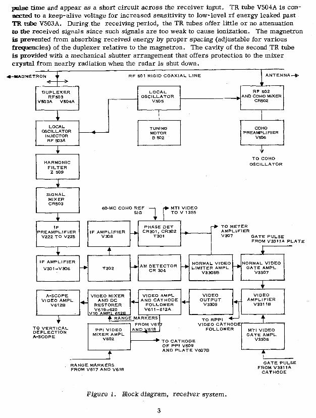
pdse time and appear as a short circuit across the receiver input. TR tube V504A is con- nected to a keep-alive voltage for increased sensitivity to low-level rf energy leaked past TR rabe VSOSA. During the receiving period, the TR tubes offer little or no attenuation to tlle received signals since such signals are too weak to cause ionization. The magnetron is prevented from absorbing received energy by proper spacing (adjustable for various frequencies) of the duplexer relative to the magnetron. The cavity of the second TR tube is provided with a mechanical shutter arrangement that offers protection to the mixer crystal from nearby radiation when the radar is shut down.
-tNETRON R F 501 RIGID COAXIAL L I N E ANTENNA
' I 1 DUPLEXER L O C A L R F 502
OSCILLATOR AND COHO MIXER V M 3 A V504A v 5 0 5 c m 2
I I
MOTOR OSCILLATOR INJECTOR R F 503A
I c, I
HARMONIC F I L T E R
SIGNAL MIXER CR503
60-MC COHO R E F MTI VIDEO SIG 1 f TO V 1355
PREAMPLIFIER
TO COHO OSCILLATOR
TO METER AMPLIFIER
GATE PULSE FROM V3311A P L A T E
VIDEO AMPL V612B
TO VERTICAL DEFLECTION A-SCOPE
4
- VIDEO MIXER VIDEO AMPL
RESTORER FOLLOWER V619--620 V611-612A
AND DC ANDCATHODE AMPLIFIER
RANGE MARKERS
VIDEO CATHODE FROM V61 P P I VIDEO ,AND Y618
Y MIXER AMPL
V602 +TOCATHODE OF PPI V609 AND P L A T E V607B 4 I
RANGE MARKERS FROM V617 AND V618
G A T E PULSE FROM V3311A
CATHODE
Figure 1. Block diagram, receiver system.
3
5. LOCAL OSCILLATOR 251 1
The tunable local oscillator assembly consists of a metal cylindrical housing, a lighthouse type triode tube V505, and circuit components. A motor-driven arrangement is provided for the remote control of tuning. An extremely stable tuned plate, tuned cathode circuit operating 60 mc above the magnetron frequency, is employed. Two coupling loops provide two separate outputs; one output is used in the receiver while the other is used in the coherent osicllator channel in gated MT2 operation.
6. LOCAL OSCILLATOR INJECTOR RF503A
The local oscillator injector RF503A provides a means of adjustable capacity coupling between the local oscillator and the echo signal from the T R cavity of V504A.
7. HARMONIC FILTER 2509
The signal output from the local oscillator injector is composed of fundamental and harmonic frequencies of both the local oscillator and the magnetron. Due to harmonic con- tent, this signal level is sufficient to materially reduce the life of the signal mixer crystal CR503. The harmonic filter provides 20 db o r more attenuation to the harmonic frequencies but little o r no attenuation to the fundamental frequencies. The total signal level impressed on the mixer crystal is thus sufficiently reduced to prevent crystal damage.
8. SIGNAL MIXER CR503
The mixer crystal CR503 acts as the first detector of the receiver system. Functionally, the first detector allows heterodyning o r beating of the local oscillator signal with the received signal. Its output contains a signal hown as the intermediate frequency, which retains the intelligence originally carried by the received echo.
9. IF PREAMPLIFIER V222, V223, V224, and V225
The output of the signal mixer crystal is an extremely low-amplitude train of 60 mc pulses occurring at the prf rate. In order to minimize noise pickup, the preamplifier is located close to the signal mixer crystal. The first two stages of the preamplifier a r e a neutralized grounded -cathode triode feeding a grounded-grid triode. The two following preamplifier stages are conventional circuits and ampllfy the 60-mc if signal to a convenient level for transmission over a coaxial line to the main if amplifier in the signal comparator.
10. 60-MC IF AMPLIFIER ASSEMBLY V301-V30S
a. The main 60-mc if amplifier assembly. This assembly includes circuits that amplify the pui ienvelope that carries the desired intelligence in the form of amplitude and phase modulation. The required intermediate-frequency gain and bandwidth are provided by six stages, V301-V306. Also included a re provisions for gain control, amplitude limiting (a requirement for phase detection when MTI is used), and a metering tube (V307) for check- ing output noise level.
4
b. T302 and AM detector. To accommodate gated MTI operation, a separate AM(norma1 radar) detector circuit consisting of T302 and CR304 is at the output of the 60-mc ampli- fia. The output of this stage is coupled to normal video amplifier V3305B.
c . IF amplifier V308 and phase detector. A second output from T302 is coupled through n arknuator to the input of V308. The attenuator is necessary to maintain the same signal amplitude at the phase detector a s was at the AM detector. The output of the phase detector is coupled to V1355. A coho adjust video signal is coupled to normal video amplifier V3305B for alining and synchronizing the coho oscillator. A third output is coupled to metering amplifier V307.
11. VIDEO BALANCER AND AMPLIFIER
a. Normal video amplifier V3305B. Either normal o r both coho adjust and normal video are amplified by this stage and coupled to normal video-limiter-amplifier V3307.
b. mI/NORMAL video-gate-amplifiers V3306 and V3307.
In normal operation, V3306 is held at cutoff by the MTI gate generator, This permits V3307 to pass signals on to video amplifier V3311B.
In gated MTI operation, V3307 is cut off and V3306 is conducting until the switchover from h4TI to NORMAL occurs. After the transition, V3306 is cut off and V3307 con- ducts. Since these 2 stages have a common plate load, either MTI o r NORMAL video is coupled on to video amplifier V3311B.
c . Video amplifier V3311B. This stage amplifies both MTI and NORMAL video signals from V3306 and V3307. Its output is coupled to the indicator cathode follower V3309 and the remote PPI cathode follower V3308.
d. Video output V3309. Cathode follower V3309 provides a low-impedance output for mansmission of the video signal to the indicator unit. Since no inversion takes place in a cathode follower, the signal remains positive at the output of V3309.
12. INDICATOR UNIT VIDEO AMPLIFIERS V611-V612A
a. The indicator unit includes two video amplifier stages, V611 and V612A, that are common to both the A-scope and PPI channels, V611 is a grounded-grid type of amplifier circuit in which the incoming positive video signal of low impedance is applied to the cathode resistor. Grounded-grid amplifiers provide improved video gain due to decreased loading of the input signal by the grid-to-cathode interelectrode capacitance. Functionally, V611 transforms low impedance (input) to high impedance (output) without inversion of the signal; thus the video signal remains positive at the output of V611.
b. V612A. An antijam circuit is included in the grid circuit of this stage and may be switched on or 08 by the ANTI-JAM switch. Video signals (positive) for both A-scope and PPI pre- sentation are obtained from separate VIDEO GAIN controls, each located in the cathode circuit of cathode follower V612A.
The positive output signals from V611 are applied to the grid of cathode follower
5

13. PF'I CHANNEL VIDEO AMPLIFIER V602 AND DC RESTORER V607B
a. Video signals (positive) for PPI display are fed from the VIDEO GAIN control in the cathode V612A to the grid of V602 in the PPI video channel. Range marker signals (negative) are applied to the cathode circuit of th is tube and result in negative video and range marker signals at the plate output of V602. These combined negative signals are applied to the cathode of PPI rube V609 and drive the cathode negative in respect to the grid, causing intensity modulation.
b. V607B clamps the PPI cathode potential to maintain ag even sweep intensity between target returns.
14. A-SCOPE CHANNEL VIDEO AMPLIFIER V619 - V612B AND DC RESTORER V620A
a. Video signals (positive) for A-scope presentation are obtained from the A-scope VIDEO GAIN control located in the cathode circuit of V612A and are fed to the grid of V619A, one-half of a twin triode tube. The control grid of the other section of this twin triode V619B is fed by positive range markers. The two plates of V619 are tied together and pro- duce negative video and marker signals that are applied to the grid of the output amplifier V612B. The positive output from V612B is directly coupled to the top vertical deflection plate of the A-scope and causes upward deflection of both video and range marker signals.
b. V620A clamps the input signals negative with respect to ground to keep the sweep constant, and prevent sweep jitter.
Section II. RF INPUT CIRCUITS
15. DUPLEXER SYSTEM RF503 (fig 2)
a. The duplexer assembly RF503 directs transmitter energy past the receiver and to the antenna; it also permits echo signals to enter the receiver without absorption by the transmitter. The system consists of two 6322 transmit-receive (TR) tubes, each mounted at the center of a tunable resonant cavity and filled with a readily ionizable gas. Tuning knobs on each cavity permit tuning over the entire frequency range of the magnetron (1,220- 1,350 mc). Tuning of the cavities is accomplished by varying the spacing of the cores in the TR tubes. Since each TR tube is mounted at the center of its resonant cavity, it is equivalent to being across the maximum voltage points of a tuned circuit. High-level rf energy from the transmitter causes the first TR tube (V503A) to ionize and short circuit the receiver input. Some energy leaks past the first TR tube and is applied to the second tube (V504A) by a short, rigid coaxial line connected between a pickup loop in the first cavity and a similar coupling loop in the V504A cavity. The second TR tube is provided with a keep-alive voltage that keeps the tube close to an ionized condition thus giving increased sensitivity to low-level rf energy. A small amount of transmitter energy passes through the second TR cavity and appears on the A-scope as the "main bang. " Since the received signal is low level, ionization of the TR tubes does not occur, and these signals enter the receiver.
6
b. The cavity of V504A is provided with a shutter arrangement that mechanically shorts the cavity and the receiver input during periods when the radar is shut down, providing pro- tection to the mixer crystal against rf energy from nearby radiation. The shutter consists of a stif€ wire that shorts the center of the cavity. The wire is withdrawn from the cavity by an armature relay K501 when the 5-minute time delay is completed. When energized, a pair of K501 contacts open and connect the high-resistance winding of the relay armature for holding. Protection against arcing of the contact points is provided by the filtering action of C523 and R526.
c. The entire duplexing assembly is connected to the rigid coaxial line RF501 by means of a slot in the line. This arrangement provides a means of adjusting the distance between tbe receiver pickoff point on RF501 and the magnetron; proper spacing results in isolation of the received signal from the magnetron. The optimum adjustment for a particular frequency (1,220-1,350 mc) is denoted by maximum receiver sensitivity.
d. The resonant cavities of V503A and V504A are tuned to the received signal frequency. Due to the odd quarter-wavelength spacing existing between. the TR cavities, the transmitter output, and the receiver input, the reflected echoes are directed to the TR cavities and away from the transmitter output circuit. This routing results in selectivity or the ability to discriminate against unwanted signals and random noise at off-resonant frequencies. This action results in greater receiver sensitivity and improved signal-to-noise ratio as well as a reduction in the effects caused by certain types of jamming. Tuning the cavities is therefore equivalent to tuning the receiver input and has a great effect on the receiver sensitivity. The selectivity curve of this tuned receiver input has a bandwidth of 6 mc.
TO I f TEST JACK 5 1 0 2 - -
1 1
PREAMPLIFIER OSCILLATM
TO OUIPUl CONNECTOR Of YAGNETROY
vso2
KEEP-ALIVE V O L T b G E
INPUT
TO LOCAL OSCILLATTOR
TO DC CONTROL CIRCUIT
I
Figure 2. Duplexer system RF503 and harmonic filter 2509.
16. LOCAL OSCILLATOR ASSEMBLY 2511
a. The local oscillator assembly consists of a 2C40 lighthouse triode oscillator tube V505, the coaxial type of circuitry associated with V505, and a motor-driven arrangement
7
for remote tuning of the circuit from the indicator unit. Basically the oscillator is an extremely stable tuned-plate, tuned-cathode circuit that operates at a frequency 60 mc higher than that of the received signal. The circuit provides two separate outputs; one is used in frequency conversion of the received echo to the intermediate frequency, and the second is employed for frequency conversion in the coherent oscillator channel for use in gated MTI operation.
b. The 2C40 lighthouse-type triode tube (fig 3(2)) is designed for coaxial circuitry, which accounts for its peculiar shape. This tube employs spoke-type grid construction (fig 3(3)), which results in extremely low interelectrode capacity as compared with con- ventional spiral-type grid construction.
c. Physically 2511 consists of concentric metal tubes (fig 3(1)) in which V505 is mounta These two concentric tubes or cylinders form a resonant coaxial line; a quarter-wavelength of this line is used in the tuned-cathode circuit and three quarter-wavelengths of the line are used in the tuned-plate circuit. The two sections are separated by a metal partition through which a feedback coupling loop passes. The equivalent circuit is shown in figure 3(4). Coarse tuning is accomplished by five adjustable paddles located between the inner and outer conductors of the cathode line. Being in the region of maximum magnetic field, adjustment of these paddles a€€ects the inductive reactance of the tuned-cathode circuit and results in a change of frequency. The position of a sliding ring mounted between the inner and outer conductors of the tuned-plate circuit provides a means of fine tuning. The ring position is controlled by tuning motor I302 through the L. 0. MOTOR switch S613A at the indicator. Two separate coupling loops at the ground end of the plate line provide the out- put voltages.
CATHOOE conxiii b l N E v PLATE COAXIAL LINE pq OUTPUT
I COUPLING T U N l N G Z S (*)
INSULATED PORTION AROUND CATHO
COUPLING LOOPS
( 1 ) LOCAL OSCILLATOR CAVITY ASSEMBLY B+
n
-CATHODE &a- - (21 L'G"THouSE TUBE ( 8 ) ISPOKE-TYPE GRID (41 EQUIVALENT CIRCUIT
Figure 3. Local oscillator details.
8

d. A cam mechanism associated with the reduction gearing of El502 adjusts the position of rhe sLiding ring mounted between the inner and outer conductor of the plate circuit coaxial section of the local oscillator assembly. The ring is composed of both metal and dielectric material with no electrical contact being made to the metal portion of the ring. When the ring is moved along the plate line, the magnetic field, the electrostatic field, or a combina- tion of both fields is affected, thus tuning the plate circuit and oscillator frequency over the latitude required.
17. LOCAL OSCILLATOR REMOTE CONTROL CIRCUIT
a. This circuit (fig 4) consists mainly of tuning motor El502, limit switches 5502 and 5503, resistors R518 and R519, and L. 0. MOTOR switch S613A located at the indicator unit (AN/TPS-16 Troubleshooting Manual, figure 8-9).
b. Tuning motor B502 has a permanent magnetic field and is reversed by reversing the poIarity of the armature voltage. The L. 0. MOTOR switch S613A at the indicator connects either ground (DEC position) or +27.5 volts (INC position) to the C519 side of the B502 armature. The side of B502 armature attached to the top of C519 also goes to the midp.int of the series circuit which includes R518 and R519 as well as the two limit switches, S502 and S503. This series circuit is connected between the +27.5-volt supply and ground. When the L. 0. MOTOR switch is in the DEC position, the C520 side of the armature is grounded, and armature current flows through R518 until S503 opens the circuit when the limit is reached. When the L. 0. MOTOR switch is turned to the INC position, the C520 side of the armature is connected to the +27.5-v01t supplys and current flows through the armature in the reverse direction with R519 now carrying the current. When the limit is reached, S O 2 opens and B502 stops. The actual operating voltage of B502 is 6 volts, the voltage drop across the resistor carrying the motor current then being 21.5 volts. Electrical noise of the B502 motor is filtered by C519 and C520.
TYIOl + TP501
R507
+21.sv
SUPPLY o--
-150 V SUPPLY
-'
SMINUTE TIME DELAY
Figure 4. Local oscillator remote control circuit.
9

Figure 5. Details of local oscillator injector RF503A.
18. LOCAL OSCILLATOR INJECTOR RF 503A (fig 5)
The output signal from the second TR cavity assembly connects to the local oscillator signal injector, the details of which are shown in figure 5. The 50-ohm resistor disk provides termination and load for the local oscillator. couples the local oscillator output and the received signal from the final TR cavity. The spacing between the coupling electrode and the center conductor is adjustable to permit variation of the degree of coupling between the two signals. The oscillator is coupled into the signal injector one-quarter wavelength away from the final TR cavity output coupling loop causing the T R cavity output coupling loop to be reflected as an open circuit. The local oscillator signal, the received echo signal, the attenuated transmitted pulse, and the harmonic energy from both the magnetron and the local oscillator are present at the output of the local oscillator injector. This combination of frequencies is now applied to a harmonic filter.
19. COHERENT INJECTOR RF502
The injector probe capacity-
The coho signal injector RF502 is similar to the local oscillator injector RF503A. This injector combines an output of the local oscillator with rf energy from the transmitter; both of these signals are applied to crystal CR502. The amount of rf transmitter energy entering the coho signal injector is controlled by an aperture o r iris between the rigid coaxial RF501 and the coho mixer RF502. The detected 60-mc signal from coho mixer crystal CR502 is used in the MTI circuitry to lock the phase of the coherent oscillator with the trailing edge of each transmitter pulse. These circuits are fully described under MTI theory.
20. HARMONIC FILTER 2509
a. The output of the local oscillator injector RF503A is comprised of the local oscillator signal, the received echo signal, and harmonics of both the magnetron and the local oscil- lator signals. The total signal level resulting is sufficient to damage the mixer crystal.
10
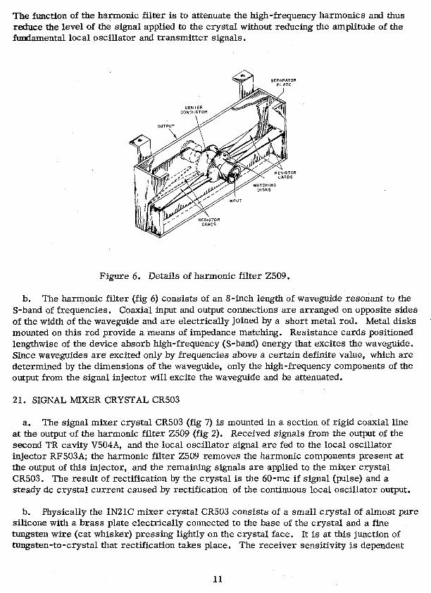
The function of the harmonic filter is to attenuate the high-frequency harmonics and thus reduce the level of the signal applied to the crystal without reducing the amplitude of the fundamental local oscillator and transmitter signals.
a SEPARATOR PLATE
Figure 6. Details of harmonic filter 2509.
b. The harmonic filter (fig 6) consists of an 8-inch length of waveguide resonant to the S-band of frequencies. Coaxial input and output connections are arranged on opposite sides of the width of the waveguide and are electrically joined by a short metal rod. Metal disks mounted on this rod provide a means of impedance matching. Resistance cards positioned lengthwise of the device absorb high-frequency (S-band) energy that excites the waveguide. Since waveguides are excited only by frequencies above a certain definite value, which are determined by the dimensions of the waveguide, only the high-frequency components of the output from the signal injector will excite the waveguide and be attenuated.
21. SIGNAL MIXER CRYSTAL CR503
a. The signal mixer crystal CR503 (fig 7) is mounted in a section of rigid coaxial line at the output of the harmonic filter 2509 (fig 2). Received signals from the output of the second TR cavity V504A, and the local oscillator signal are fed to the local oscillator injector RF503A; the harmonic filter 2509 removes the harmonic components present at the output of this injector, and the remaining signals are applied to the mixer crystal CR503. The result of rectification by the crystal is the 60-mc if signal (pulse) and a steady dc crystal current caused by rectification of the continuous local oscillator output.
b. Physically the IN21C mixer crystal CR503 consists of a small crystal of almost pure silicone with a brass plate electrically connected to the base of the crystal and a fine tungsten wire (cat whisker) pressing lightly on the crystal face. It is at this junction of tungsten-to-crystal that rectification takes place. The receiver sensitivity is dependent
11
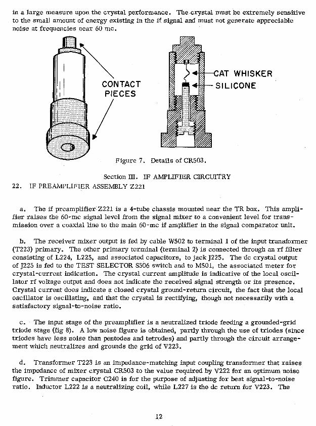
in a large measure upon the crystal performance. The crystal must be extremely sensitive to the small amount of energy existing in the if signal and must not generate appreciable noise at frequencies near 60 mc.
WHISKER .ICON€
Details of CR503.
Section III. IF AMPLIFIER CIRCUITRY 2 2 . IF PREAMPLIFIER ASSEMBLY 2221
a. The if preamplifier 2221 is a 4-tube chassis mounted near the TR box. This ampli- fier raises the 60-me signal level from the signal mixer to a convenient level for trans- mission over a coaxial line to the main 60-mc if amplifier in the signal comparator unit.
b. The receiver mixer output is fed by cable W502 to terminal 1 of the input transformer (T223) primary. The other primary terminal (terminal 2) is connected through an rf filter consisting of L224, L225, and associated capacitors, to jack 5225. The dc crystal output of J225 is fed to the TEST SELECTOR S506 switch and to M501, the associated meter for crystal-current indication. The crystal current amplitude is indicative of the local oscil- lator rf voltage output and does not indicate the received signal strength or its presence. Crystal current does indicate a closed crystal ground-return circuit, the fact that the local oscillator is oscillating, and that the crystal is rectifying, though not necessarily with a satisfactory signal-to-noise ratio.
c. The input stage of the preamplifier is a neutralized triode feeding a grounded-grid triode stage (fig 8). A low noise figure is obtained, partly through the use of triodes (since triodes have less noise than pentodes and tetrodes) and partly through the circuit arrange- ment which neutralizes and grounds the grid of V223.
d. Transformer T223 is an impedance-matching input coupling transformer that raises the impedance of mixer crystal CR503 to the value required by V222 for an optimum noise figure. Trimmer capacitor C240 is for the purpose of adjusting for best signal-to-noise ratio. Inductor L222 is a neutralizing coil, while L227 is the dc return for V223. The
12

N O
Y : 0 c
I
13

third and fourth if amplifiers (V224 and V225) employ.conventiona1 circuits. The output of the last amplifier, V225, is coupled by matching transformer T222 through jack J227 and a coaxial cable to the unit output connector J507.
23. RECEIVER BANDWIDTH REQUIREMENTS
a. Pulse modulation of the radar transmitter results in the formation of two distinct modulation components. One component consists of the pulse rate (prf) and its harmonics, while the other is comprised of the carrier fundamental and its odd harmonics that make up the rectangular transmitted pulse. These modulation components give rise to upper and lower sidebands by adding and subtracting from the carrier frequency. Thus the trans- mitter r f output is a spectrum of frequencies in which each frequency above the carrier has its counterpart in another frequency equally spaced below the carrier; the ideal spectrum is symmetrical about the carrier frequency. In order for the receiver to respond to a maximum of energy in the transmitter spectrum and at the same time respond to a minimum of random noise, an important relation must exist between the spectrum frequency width and the receiver bandwidth. This relation is graphically presented in figure 9 which shows an optimum receiver response curve superimposed upon an ideal spectrum. Note that the receiver bandwidth (half-power points of the response curve) is equal to the frequency width of the transmitter main lobe.
Figure 9. Receiver response on transmitter spectrum.
b. The relationship between the required radar receiver bandwidth for a given trans- mitter pulse width is expressed as follows:
Bandwidth in megacycles = 2 Pulse width in psec?
Applying this formula to the AN/TPS-lG it is seen that the 2-psecond transmitter pulse width results in a required 1-megacycle receiver bandwidth. This requirement means that the overall receiver-from the first TR tuned cavity to the cathode-ray tubes-must be
14
capable of passing all signals one-half megacycle above or below the frequency of the trans- mitter. Any transmitter spectrum energy that lies outside the receiver bandwidth is lost; the effect is the same as if the transmitter power were reduced.
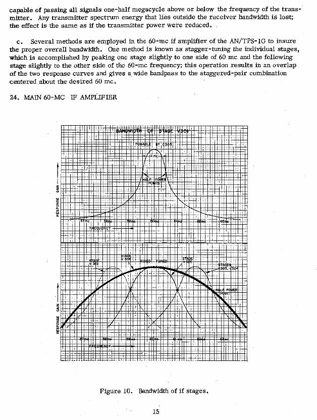
c. Several methods are employed in the 60-mc if amplifier of the APJ/TPS-lG to insure tbe proper overall bandwidth. One method is known as stagger-tuning the individual stages, which is accomplished by peaking one stage slightly to one side of 60 mc and the following stage slightly to the other side of the 60-mc frequency; this operation results in an overlap of the two response curves and gives a wide bandpass to the staggered-pair combination centered about the desired 60 mc.
24. MAIN 60-MC F AMPLIFIER
Figure 10. Bandwidth of if stages.
15
a. The first stage, V301, can be tuned (C305) over a 4-mc range around 60 mc without changing overall receiver bandwidth and gain. The stage has a bandwidth of approximately 1 mc (fig 10 (1)). Gain control is provided at the indicator unit by means of R608 or by the I-F AMPL LEVEL control R2350 at the signal comparator unit depending upon the position of OPERATION SELECTOR switch S2354.
b. Following the first stage are two staggered-tuned pairs of amplifier stages, V302- V303 and V304-V305. These four stages are fixed-tuned about a center frequency of 60 mc (fi9 W2)).
c. The final 60-mc, if amplifier (V306) is a broadband, fixed-tuned stage, the output of which drives the detector through an overcoupled transformer T302. The use of over- coupling between these stages results in broadening the bandpass. The bandwidth of the if amplifier from the plate of the second stage to the detector is approximately 5 mc. This bandwidth may shift as the components age. Adjusting C305 provides peak performance during this aging process.
d. The bias circuits of V304, V305, and V306 are arranged to provide limiting action, a requirement for phase detection used with MTI. The control grids of these tubes are operated at approximately 50 volts above ground through the use of voltage dividers. The cathode resistors employed in these stages are large enough to develop just over 50 volts; this places the grids slightly negative in relation to the cathodes. Since the effective plate voltage of these tubes is approximately 75 volts, a small signal input voltage swing (less than one volt) results in the positive portion of the output signal being limited by plate saturation and the negative portion by cutoff.
e. The last if amplifier (V306) is followed by two distinct,types of detector circuits: one provides conventional amplitude modulation (AM) detection of the echo signal for normal radar display; the second provides phase detection of the echo and coho signals for MTI display. Normal amplitude detector CR304 and its associated circuits provide normal video detection during gated MTI operation. The other detector consists of crystals CR301 and CR302 which function as a phase detector to provide MTI operation.
f. Phase detectors CR301 and CR302 also provide two dc voltages for adjustment- checking in conjunction with internal test meter M2350. One voltage indicates coho level, the other indicates if amplifier signal level. The low value of C375, between T302 and the grid of if amplifier, V308, limits the signal level at the grid of V308 to that of the signal at V306. This insures the same signal level at the phase detectors (CR301 and CR302) as at the normal video detector (CR304).
g. The output of the phase detector is fed directly to the 9-mc oscillator in the MTI repetition rate trigger amplifier. When the radar is used as a normal system, the coho oscillator signal is removed and normal radar video signals are obtained from CR304, which demodulates the 60-mc signals into load resistor R336. The video signal (negative) is then fed to V3305B, in the video balancer and amplifier circuit, through the contacts of K3300 and K3301. To adjust either the coho oscillator or the received signal voltage, the voltage developed across C334 is sampled. Since the coho oscillator voltage is continuous wave, it develops a direct voltage across C334. This dc voltage is supplied to test meter
16

iM2350 via test selector switch S2353. The metering circuit is isolated from the detector signal circuit by R2358 and R2363. Received signal video voltage is amplified by V307, rectified and filtered by CR303, R331, and C341, and then fed to the metering circuit. This voltage is the if amplifier signal level mentioned earlier. The signal level is adjusted by means of potentiometer R2350. This control permits adjustment of the bias on the first and third if stages and, consequently, adjusts the gain of these stages. Inductor L307, in the grid circuit of V307, isolates V307 from the detector output circuit.
25. VIDEO BALANCER AND AMPLIFIER
a. The negative video signals a re fed to the normal video amplifier V3305B, where limiting is accomplished by operating the stage at a very low plate voltage. Positive signals are passed through C3313 to the grid circuit of V3307, the limiter amplifier. The voltage divider network, consisting of R3339 and R3336, establishes a bias of approximately -3 volts on V3307. CR3308 is a dc restorer that conducts when the signal tries to go below -3 volts and thus sets the dc level.
b. Relays K3300 and K3301 operate to close the cathode and grid circuits of V3305B. When OPERATION SELECTOR S2354 is in COHO ADJUST position, K3300 operates to include the cathode degeneration resistor R3356 and thus decreases the gain of V3305B. During NORMAL and GATED MTI operation, K3300 and K3301 feed normal video from CR304 of the 60-mc if amplifier to the grid of V3305B. During COHO ADJUST operation, 60-mc phase-locked signals are fed to the grid of V3305B through alternate contacts of K3300 and K3301.
c. The output of V3305B is fed to the control grid of V3307. V3306 and V3307 are both operated with approximately -3 volts on their grids; however, actual conduction is a func- tion of the gating pulse, fed to the suppressor grid of each stage, from the MTI gate gener- ator. While one stage is conducting as a result of positive signal (gate-pulse) to its sup- pressor grid, the other stage is cut off due to a negative signal to its suppressor grid. The conducting stage is then cut off and the original cutoff stage conducts. Thus, gated MTI is produced by electronic switching of normal radar o r MTI signals to the indicator.
d. The parallel-connected plates of V3306 and V3307 then pass the signal on to V3311B, where both normal and MTI signals a re amplified. Limiting is accomplished by operating the stage into the diode-limiting circuit consisting of CR3302, CR3303, R3341, R3342, R3343, and R3344. With no signal applied, CR3302 is conducting continuously, and the voltage divider R3344/R3343 establishes the voltage across R3343 at approximately 50 volts. Limiter control R3342 is adjusted for a voltage of approximately 54 volts at the junction of R3342 and CR3303. When the positive video signals are passed through C3308 and applied across R3343, CR3302 ceases to conduct, and the stray capacity existing between ground and the junction of the two diodes immediately starts charging toward 150 volts. The capacity is very small, and the rise time is therefore very small. When the plate side of CR3303 tries to rise above the cathode side, the diode conducts and limits the signal level to the voltage set by R3342.
i
e. The limited video signals from V3311B are fed to cathode followers V3308 and V3309, the grid circuits of which are parallel-connected although the cathode circuits provide
1.7
separate outputs. V3309 feeds video signals to the indicator through 5303. V3308 provides video on a 70-ohm circuit for remote indicator use; a 150-ohm, l-watt resistor is required at the indicator end of the circuit. The output of V3308 also is available at test point TP301 for tuning purposes. It is also necessary to use a 150-ohm resistor across the meter o r other test equipment when using TP30 1.
.26. METERING TUBE V307
To monitor either the coho oscillator o r the if amplifier noise voltage, the voltage across C334 is sampled. As the coho oscillator is cw, it develops dc across C334. This voltage is supplied to test meter M2350 via test selector switch S2353. The if amplifier noise voltage is amplified by V307, rectified and filtered by CR303 and R331-C341, then fed to the metering circuit. Inductance E307 isolates V307 from the detector output circuit.
Section IV. VIDEO CHANNEL
27. COMMON INDICATOR VIDEO STAGES V611 and V612A
a. The indicator unit accepts the positive normal o r MTI video signal for further amplification and display on the PPI and A-scope. The indicator video channel includes provisions for introducing range markers and reducing the effect of certain types of jamming, each of which is effective on both scopes. The video amplifier system in the indicator con- sists of input amplifier V611 and cathode follower V612A, each common to both scopes; following these common stages a re separate video channels for the PPI and A-scope. The A-scope channel consists of video-range marker mixer V619, V620A dc restorer, and V612B the final video amplifier. The PPI channel is made up of IFF video-strobe marker mixer V601, which is followed by V602, an amplifier-mixer that combines radar video and range marker signals. The combined signal, after dc restoration by V607B, is applied to the cathode of the PPI tube.
b. The incoming positive video signal is first amplified by V611, a grounded-grid amplifier using a triode-connected pentode that produces a high-impedance positive output from the low-impedance (coaxial line) positive input. The output signal of V611 is applied to the grid of cathode follower V612A. The coupling between the stages includes an antijamming network that may be switched in o r out of the circuit by ANTI-JAM switch S607. The antijam circuit consists of L603, CR601, R674, and R679. With S607 in the ON position, R679 is shorted. The resulting circuit is a high-pass filter. Thus, only the leading edges of all echoes (including jamming signals) a re passed, which results in a reduction of their blanketing effect. When S607 is in the open position for normal radar operation, the impedance of the grid circuit of V612A passes the video envelope. Crystal diode CR601 maintains the grid of V612A at the proper dc operating level and removes the undesirable negative dip in the signal that results from high-pass filtering. Note that cathode follower V612A has two outputs, each taken from separate video gain controls, R682 and R683. These two output video signals (positive) are channeled to the PPI and A-scope circuits.
18

28. PPI VIDEO MIXERS V601 and V602
Positive radar video signals are taken from video gain control R682 in the cathode cir- cuit of V612A and applied to the control grid of V602. Negative 5- o r 25-mile range marker pulses, if used, are applied to the cathode of V602 via separate marker intensity controls R1617 and R1629 through S606 sections D and E. Thus, V602 performs mixing and amplification of radar video and range marks, which appear as negative signals at the plate. Note that V601 (IFF VIDEO AND STROBE MIXER) and V602 share a common plate load (parallel resistors R616 and R617), which results in mixing the signal outputs of each tube. Thus, in the common plate circuit of V601 and V602 there are the radar video and strobe marker signals and when desired IFF video and range markers, all of which are negative. After dc restoration by V607B, the composite negative signal is applied to the cathode of the PF'I tube causing intensity modulation.
29. A-SCOPE VIDEO CHANNEL V619, V620B, AND V612B
The positive video signal for A-scope presentation is taken from video gain control R683 in the cathode circuit of V612A and applied to the grid of V619A (pin 2). The plate load of V619A is common to V619B, the A-scope range marker amplifier. Thus both the radar video signal and range markers appear in the common plate circuit of V619 as negative signals. The signal is coupled to the grid of V612B and is dc restored by V620A to insure that the video range marker signal has no positive signal component. The positive output from V612B is direct-coupled to the top vertical deflection plates of the A-scope tube V625, resulting in.an upward deflection for both radar video and range marker pulses.
30. MISCELLANEOUS CIRCUITS
a. Keep-alive voltage power supply. The second TR tube in the rf system, V504A, is supplied with a keep-alive voltage from a half-wave power supply located in the receiver- transmitter unit. This voltage is about -600 volts with V504A conducting and -800 volts when V504A is nonconducting. This power supply consists of V501, transformer T501, RC filter C501, C502, and R505. A bleeder circuit from output to ground consists of R501 through R504.
b. Local oscillator filament supply. Direct current is used on the filament of the receiver local oscillator V505 to prevent the possibility of amplitude modulation o r fre- quency modulation being introduced into the cathode circuit. The dc voltage is obtained &om the positive 27.5-volt power supply and is stabilized by series ballast tube TY501; additional filtering is provided by L501 and C503 (fig 4).
c. Filament circuits. AC filament power at 6.3 volts is provided for the receiver preamplifier V222, V223, V224, and V225, as well as for the coho preamplifier V506, by &us fo rmer T503. Isolation between stages is supplied by choke coils L223, L233, and L228; additional isolation is provided by C238, C226, C233, C237, and C529. Filament power for the main 60-mc if amplifier and the video balancer amplifier is supplied at 6.3 volts by transformer T2350. Interstage coupling through the filament circuit is prevented
19

in the main if amplifier by L308, C338, C331, etc. The indicator unit video channels receive filament power at 6.3 volts ac from transformer T605.
d. Receiver relay switching functions. K501, located in the receiver-transmitter rf system, mechanically removes a short circuit at the receiver input when the radar is in operation. When the radar is shut down, a length of stiff wire or shutter shorts the center of the cavity of the second TR tube V504A thus protecting the receiver mixer crystal CR503 against rf energy entering the antenna from other radars. The wire shutter is withdrawn externally by the armature-type relay K501 when energized. A pair of K501 contacts con- nects into the circuit the total high resistance of the relay armature coil for holding the armature in position when K501 is energized. Protection from contact arcing is provided by C523 and R526 filtering action. Following the rf system, the normal radar includes two relays, K3300 and K3301, each located in the signal comparator unit and controlled by the OPERATIONS SELECTOR switch, S2354. When in the REMOTE position, section D of S2354 allows the gain of the receiver to be controlled at the indicator unit by the REC GAIN control R608 by the switching action of S2354D and relay K3301; in all other positions of S2354 the gain of the receiver is controlled by the I-F AMPL LEVEL control R2350 at the signal comparator. When S2354 is in the normal position, K3301 is operated to short out the degenerative cathode resistor R3356 and thus increase the gain of V3305B. At this time, normal video is also applied through contacts of K3301 and K3300 to V3305B. Other positions of S2354 provide GATED MTI operation or COHO ADJUST through the energizing or deenergizing of K3301 and K3300 contacts.
Section V. PREVENTIVE MAINTENANCE
31. TR TUBE SELECTION
Defective TR tubes frequently are the source of poor receiver performance. A defective TR tube can be the cause of frequent crystal-mixer failure and may cause excessive TR bandwidth or excessive TR recovery time. For these reasons, TR tubes should not be used beyond their normal life expectancy of 500 hours. It is good practice to keep a log of hours of use, using the OPERATING HOURS meter M402 on the power supply for elapsed time indication. A TR tube that has deteriorated beyond usefulness is evidenced by a lack of response to TR cavity tuning. The only practical method of determining a good TR tube is by comparison of radar performance with a new tube.
32. CARE, CHECKING, AND SELECTION OF IN21C CRYSTALS
a. Care of crystals. The receiver sensitivity is dependent to a large measure upon crystal-mixer performance. Since the crystal must be extremely sensitive to very small amounts of rf energy and must not generate appreciable noise at frequencies near 60 mc, the result is that the crystal is fragile both electrically and mechanically. The crystal must not be subjected to mechanical shock (dropping) or excessive current. Mechanical shock may cause a change of tension at the junction point of the tungsten wire cat whisker and the silicon, the point where rectification takes place (fig 7). Excessive current causes heat at the junction point which may burn the thin tungsten wire or melt the silicon at the junction point. Rules for proper crystal care may be summarized as follows:
(1) Always handle crystals with care.
20
Crystals should be wrapped in metal foil when carried or stored to provide pro- tection against r f energy usually present near a radar.
The static electrical charge built up in the human body may reach a potential high enough to damage the crystal if allowed to discharge through it. This possibility of damage can be avoided by grounding the body to the metal framework of the radar before unwrapping or changing the crystal.
Never exceed the recommended crystal current.
Avoid the use of defective TR tubes or those that have exceeded the 500-hour normal life expectancy.
b. Checking crystals. When the adjustment of the local oscillator coupling will not bring the crystal current to the red-line value on M501, the trouble is either that the local oscillator is not oscillating strongIy enough or, more likely, the rectifying properties of the crystal have deteriorated. If the coho crystal current is normal and the signal crystal current low, the local oscillator is definitely normal. L€ a crystal checker is not available, there are two other methods of checking a crystal. One method is to measure the front-to-back resist- ance ratio of the crystal with an ohmmeter; a good crystal will have a ratio of 18: 1 or greater. When checking a crystal with an ohmmeter, never use a resistance range less
The second method consists of placing the crystal to be checked in the metering circuit of the echo box and comparing the echo box meter reading with that of a crystal known to be good. This method is far superior to the ohmmeter method in that the test is made at radar frequencies. Either method of checking does no more than segregate crystals that are definitely bad from those that are possibly good. Since neither method indicates the signal-to-noise ratio of the crystal, the final criterion is the performance in the radar as indicated by a receiver sensi- tivity test.
I
than R x 100, otherwise the ohmmeter current will damage the crystal. I
c. ratio. One of the main sources of noise (and consequently one of the circuit elements that causes a lowering of signal-to-noise ratio) is the crystal mixer. Some crystals generate more noise in the 60-mc region than others; it is, therefore, imperative that a careful selection of the mixer crystal be made, fully noting the sensitivity of the receiver with each crystal. Mechanical shock or excessive current also changes crystal noise characteristics; therefore, the rules outlined in (1) and (4) above apply here also.
Crystal selection. A s previously stated, the receiver requires a high signal-to-noise
Section VI. RECEWER ADJUSTMENTS AND PERFORMANCE CHECKS
33. RECEIVER ADJUSTMENTS
a. Preliminary steps.
(1) Be sure that the power supply, modulator, transmitter, and indicator have been properly adjusted before proceeding with the following adjustments.
21

i
(2) Slide the RECEIVER-TRANSMITTER out of the case to its locking catches and close the RCVR-XMTR INTERLOCK S504.
(3) Set the POWER switch S602 at ON.
b. Adjustments.
Set the controls on the units in the following order:
CONTROL - UNIT SETTING
RADIATE switch S616 INDICATOR ON
OPERATION SELECTOR S2354 SIG COMP REMOTE
OPERATION S60 1 INDICATOR NORMAL
A-scope VIDEQ R683 IADICATOR 1-inch video
RECEIVER GAIN R608 INDICATOR 4 -inch grass
RANGE SELECTORS S606 & S609 INDICATOR 20 miles
TEST METER switch S506 RCVR-XMTR SIG
RADIATE switch S615 INDICATOR OFF
OPERATION SELECTOR S2354 SIG COMP NORMAL
TEST METER M2350 SIG COMP IF AMPL LEVEL
Adjust C305 for maximum deflection on TEST METER M2350 (this reading may be greater than red line).
Adjust the IF AMPLITUDE LEVEL control R235O fo r a red-line reading on TEST METER M2350. Adjust local oscillator injector RF503A fo r red-line reading on TEST METER M501.
Make the following control settings:
UNIT SETTING
OPERATION SELECTOR S2354 SIG COMP REMOTE
RADIATE S616 INDICATOR ON
__c CONTROL
Position the antenna on a fixed target.
22
Hold L. 0. MOTOR switch S613 in the INC position for a few seconds.
Tune the L. 0. MOTOR down from the high-frequency extreme by holding the L. 0. MOTOR switch S613 in the DEC position until maximum target echo amplitude is observed on the range (A) scope.
In finer tuning, turn the L. 0. MOTOR switch ,5613 back and forth between INC AND BEG until maximum target echo amplitude is indicated.
If the target echo being observed while tuning saturates the scope, reduce the amplitude by adjustkg RECEIVER GAIN control R608 before continuing with tuning procedure.
Set the TEST SELECTOK switch S506 to SIG.
Adjust the local oscillator injector RF503A for 2/3 red line reading on the TEST METEk.
Set the TEST SELECTOR switch S506 to COHO
Adjust the CQHO injector RF502 for red line reading on the TEST METER.
Adjust the two TR tubes V503 and V504 for maximum target echo amplitude on the range (A) scope.
Retouch the adjustment of each tube to insure fine tuning.
Tune the duplexer assembly RF503 by loosening the two clamps and sliding the assembly back and forth until maximum target echo amplitude is obtained.
Adjust the local oscillator injector RF503A for maximum signal to noise ratio as observed on the range (A-) scope.
Adjust the RECEIVER GAIN control R608 for approximately t inch of grass on the range (A-) scope.
First, turn the A-scope VIDEO GAIN control R683 fully counterclockwise, then adjust the control slowly clockwise until the echo signals reach maximum amplitude.
NOTE: When further adjustment does NOT increase the signal amplitude, but DOES increase the noise level, back off on the control until the signals are just at maximum amplitude.
34. SYSTEM PERFORMANCE DETERMINATION
a. Concept of radar performance figure. Of all the factors affecting the ability of a radar set to detect small or distant targets, only the performance of the radar set can be controlled by maintenance personnel. The importance of measuring radar performance must be emphasized, and the measurement should be made frequently at scheduled intervals.
23

The term radar performance figure describes an overall figure of performance merit of an entire radar system. Using the analogy of sound echoes, the strength of an echo is determined by the ability of a man to shout and equally by his ability to hear. Thus, radar performance can be improved equally through an improvement in the ability to receive weak signals as well as through an increase of the transmitted power output. The ability of the receiver to receive weak signals is measured by noting when the signal power input is just barely discernible from the receiver noise. This receiver input is known as the mini- mum discernible signal; the ratio of peak transmitted power to the minimum discernible sig- nal is the performance figure. Since the ratio deals with quantities of a magnitude that can be dealt with more conveniently by logarithms, both peak transmitter power and minimum discernible signal (MDS) are expressed in decibels. Although the performance figure is calculated on a logarithmic basis by the use of decibels, it is not required that maintenance personnel have a working knowledge of either logarithms or decibels since the values dealt with are obtained from meter readings rather than from any involved mathematical calcu- lations. Those who desire additional information about the mathematical calculations and the interpretation of measurements, may see TM 11-759, Theory and Measurement of Pulse Radar Performance.
b. Average power measurement.
Connect bolometer (DT-76/U) to UG- 88/U coax connector of summation bridge TS-730/LJRM.
Turn selector switch to SET ZERO position.
Turn ON-OFF switch to ON and allow 20 minutes warmup time and position the antenna in a clutter-free area.
Connect 10-db attenuator CN-llO/U to bolometer DT-76/U using screws provided in power measuring kit MX-1309/URM-23. Using the same fastening screws, con- nect adapter UG-402/U to opposite end of attenuator.
Set COMPENSATE A'ITENUATOR dial to zero.
After warmup with the selector switch in SET ZERO position, adjust the SET ZERO control until the galvanometer M12 is balanced at zero.
Rotate the selector switch to CALIBRATION LEVEL position (reading on red scale of power meter M101).
Rotate the selector switch to ADJUST CALIBRATION position. Vary the ADJUST CALIBRATION knob until the reading obtained in step (7) is read on the black scale of the power meter M101. The summation bridge is now calibrated for use.
NOTE: The bolometer element is extremely sensitive to even slight changes in temperature. If the selector switch is left in either the CALIBRATION LEVEL or ADJUST CALIBRATION position for more than a few seconds, the switch should be returned to SET ZERO position, and steps (6) through (8) should be repeated. Be sure that the rf input is removed from the bolometer head before adjusting SET ZERO control.
24
(9) Connect rf power J-SO1 to bolometer using cable CG-92B/U. This cord is provided in power measuring kit MX-1309/URM-23.
(10) Rotate the selector switch to ADJUST BALANCE position. Vary the ADJUST BALANCE knob until the galvanometer pointer is center at zero after stabilization ' (do not readjust SET ZERO control).
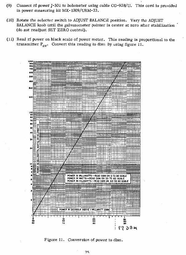
(11) Read rf power on black scale of power meter. This reading is proportional to the transmitter Pav. Convert this reading to dbm by using figure 11,
Figure 11. Conversion of power to dbm.
25
I. R A D A R K T SERIAL NO. 11. TEST EPUlPMeNT
111. OBSERVER SERIAL, NO.
IV. DATE SERIAL NO.
RADARPERFORMANCEFIGURE
CONVERSION OF POWER TO dbm
RATED RADAR PERFORMANCE
Radar Set Peak Power-dbm MDS-dbm Rated overall Performance -clb
190 to 192 AN/TSS 1G 87.6 to 87.9 -102.3 to -104.0
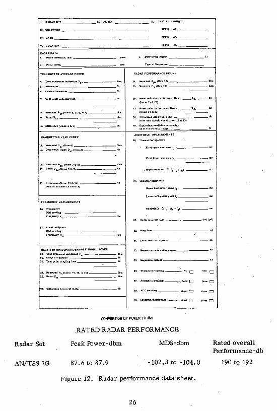
Figure 12. Radar performance data sheet.
26

(12) To obtain transmitter average power, items (4) through (7) on the radar per- formance check sheet, figure 12, must be completed. The procedure is as follows :
(a) Enter in item (4) the test equipment indication found in step (11) above.
(b) Enter in item (5) the 10 db of the attenuator CNllO/U.
(c) Enter in item (6) the cable attenuation of 0 .5 db for the entire frequency range.
(d) Enter in item (7) the test point coupling loss indicated in figure 13.
(e) Enter in item (8) the sum of items (4) through (7).
c . Transmitter peak power calculation, items 11 - 15.
(1) Enter in item 11 measured transmitter average power (dbm) . (2) Determine duty cycle figure (db) from nomograph in figure 14 and enter in
item 12.
(3) Add (1) and (2 ) above to obtain transmitter peak power and enter this value in item 13.
(4) The rated peak power of the AN/TDS-lG, 87.6-87.9 is then entered in item
(5) Enter the difference between rated peak power and calculated peak power.
(15).
d . Radar performance figure. Measured transmitter peak power plus measured receiver MDS equals radar performance figure. Use signal generator TS-419/U for measuring Pm (minimum discernible signal power) of the AN/TPS-lG as follows:
(1) Energize AN/TPS- 1G and allow 30 minutes warmup. Tune radar for best pos- sible performance and position the antenna in a clutter-free area.
(2) Connect power cord to TS-419/U, put POWER switch in ON position and allow 20 minutes warmup.
(3) Using adapter UG-201/U and 8-foot coaxial cable (RG-58/U) connect IFF sync (J418, AWTPS-1G) to sync-in jack TS-419/U.
(4) Using adapter UG-POl/U and 6-foot coaxial cable (RG-55/U) connect rf test (JSOl, AN/TPS-1G) to rf output jack TS-419/U.
(5) On the TS-419/U, with the SELECTOR switch in the ZERO SET position, adjust the ZERO SET knob so that the meter needle reads zero set . Lock the ZERO SET knob being careful to observe that the meter needle does not move.
(6) On the TS-419/U, with the SELECTOR switch in the CW position, adjust the POWER SET knob so that the meter needle reads on the red line marked POWER SET. Lock the POWER SET knob being careful to observe that the meter needle does not move ~
27

1100 '
1050
>. m
3 I
c
v
1000 I- z W I w ix 3
950 W 5
K w c W 5
a 900 W 3 0 a >. -I a 5 850 3 5
-
800
1200 1220 1240 1260 1280 1300 1320 1340 1369 F R EQ U E N CY ( M EGAC Y CLES)
Figure 13. Test point coupling attenuation.
28

FINDIN6 WlY-CYCLE FJWRE
I WSTRUCTI OW%
1. Obtain d a b on radar se t 4000 regarding:
a- Pulse length in micro- seconds.
b. Repetition r a t e (PRF) i n pulse$ per remnd.
‘O0 3. Using nomograph, the duty- cycle f igure for the above
800 conditions i s found to be 32.2 db. (This value must be added t o the average power I n dbm to obtain the peak power i n dbm.)
Figure 14. Determining duty-cycle figure (in db) . On the TS-419/U, with the SELECTOR switch in the CW position and the output attenuator set at minimum attenuation, rotate the SIGNAL FREQUENCY knob until the A-scope on the AN/TPS-1G is saturated by the output from the TS- 419/U. This operation tunes the signal generator output frequency to the approximate frequency of the receiver.
On the TS-419/U, the SELECTOR switch in POSITIVE SYNC, the PULSE WIDTH set to 2 microseconds, the PULSE RATE set to 400 pps, vary the PULSE DELAY knob until the pulse output from the TS-419/U can be seen in a clutter-free area on the radar A-scope . Rotate the OUTPUT ATTENUATOR knob until the pulse output from the signal generator does not saturate the radar A-scope. Adjust the SIGNAL FREQUENCY knob until the pulse height on the A- scope is of maximum amplitude. This operation tunes the signal generator out- put frequency to the exact frequency of the receiver. Repeat steps (5)and ( 6 ) . Then return SELECTOR switch to POSITIVE SYNC.
While observing the pulse on the radar A-scope, rotate the OUTPUT ATTENU- ATOR knob counterclockwise until the pulse just disappears into grass level. Read the attenuation (dbm) on the attenuator dial. Repeat this step several times, recording each reading, and average these readings for the final TS- 419/U reading in dbm . Calculate the receiver minimum discernible signal power in the following way (refer to TM 11-759, page 58) and (refer to the radar data performance sheet, figure 12, for item numbers).
“I7
Test equipment indication (-dbm)
Cable attenuation (obtain information from TS-419/U Maintenance Handbook, page 5-2)
Test point coupling loss (obtain from figure 13
Measured Pm (dbm) a+&
Rated Pm (dbm) for AN/TPS-1G
Should be 72 dbm o r more; obtained in step (9).
Approximate reading;
1.2 db
Approximate reading ; 28.0 db
- 105.2 db
-102.3 to -104.0 dbm
Difference e-d fl.2 db
(1 1) The manufacturer of the AN/TPS- 1G radar, as indicated in figure 12, rates the peak power expressed in dbm, a s +87.9 and the minimum discernible sig- nal power (P,) a s - 1021 3 to - 104 .O dbm giving an overall performance figure of 190 to 192 dbm . An example of rating the TPS- 1G performance is given below:
Example
Measured peak power 84 dbm
Plus measured MDS power (Pm) 99 dbm
Equals measured overall performance 183 db
Optimum performance (100 percent) 1 9 1 db
Less measured overall performance 183 db
Equals sensitivity loss in db 8 db
To convert db loss to percentage of maximum range available, check against the conversion table of figure 15.
(12) It can be seen from the conversion table that a radar set performance figure need be down only 12 db for the set to be operating at only 50 percent of maxi- mum range. In many instances this deficiency can be caused by weak tubes, faulty crystals, dirty rf lines, o r misalinement . By proper use of the test equipment and corrective maintenance, the set can be made to operate at peak efficiency. Nothing but peak performance should be tolerated.
(13) It can be seen from the conversion table that it is useless to assess the value of a radar site with the radar operating below maximum performance, and it is suggested that full utilization be made of the test equipment to insure maxi- mum performance from the AN/TPS- lG radar.
30

Approximate % of vlax Range Availabk
100
97
94
89
84
80
75
71
67
63
60
db Below Opti- num Performance
10
11
12
13
14
15
16
17
18
19
20
Approximate % of lax Range Availabla
56
53
50
47
45
42
40
38
36
34
32
Figure 15. Conversion table.
Section VII. SUMMARY AND QUESTIONS
35. SUMMARY
The AN/TPS-1G radar receiver is a superheterodyne. The rf signals are intercepted by the same antenna system previously described in the text on the transmitter and rf system (ST 44-188-3G). The receiver is protected from transmitted energy by two TR tubes located in the portion of the waveguide system called the duplexer. The rf energy intercepted travels tkrough the TR tube to the signal mixer where it is mixed with the output-of the stable local oscillator. The difference frequency (intermediate frequency) o 60 mc is amplified in the if preamplifier and main if amplifier. The if envelope is then detected, and the resulting video signal is amplified and applied to the cathode-ray tubes. The receiver is designed to keep the signal-to-noise ratio as high as possible. A design feature which is particularly helpful in keeping noise from being mixed with the signal is the placing of the if preamplifier close to the crystal mixer; this location requires only a short cable which picks up very little noise and offers negligible signal attenuation. The first two stages of the if preamplifier are designed to produce a minimum of noise. The range capability of a radar is expressed by the performance figure, which is a function of peak transmitter power and receiver sensitivity. Lack of receiver sensitivity may be caused by the following.
a. Defective signal mixer crystal or TR tubes.
b. Receiver tuning.
c. Defective preamplifier tubes.
31

3 6 . QUFSTIONS
a . Why does the receiver circuit include both an if and video gain control?
b . bandwidth.
Explain the relation between the transmitter pulse width and the required receiver
c . Describe the local oscillator circuit.
d . Explain two methods of testing a type 1N21C crystal.
e. Upon what principle does the antijamming circuit function?
f . Define the following terms:
(1) Minimum discernible signal.
(2) Heterodyning.
( 3 ) Bandwidth.
(4) Duplexer .
(5) Frequency conversion.
What is the function of test meter MSOl? g .
h. Describe the steps in locating the causes of a poor receiver MDS power (P,) .
i . What data a re required to compute the performance figure of a radar set?
32

INDEX
Paragraph Page
Adjustments . . . . . . . . . . . . . . . . . . . . . . . 33 21
Cascade . . . . . . . . . . . . . . . . . . . . . 22 12 IF main assembly . . . . . . . . . . . . . . . . . 10, 24 4, 15 IF preamplifier . . . . . . . . . . . . . . . . . . 9, 22 4, 12 Video, A-scope channel . . . . . . . . . . . . . . . 14, 29 6, 19
Video stages in indicator . . . . . . . . . . . . . . 12 5
Amplifiers :
Video, PPI channel . . . . . . . . . . . . . . . . . 13 6
Video, stages in signal comparator. . . . . . . . . . . 25 17 Antijamming, provision for . . . . . . . . . . . . . . . . . 27 18
Bandwidth requirements . . . . . . . . . . . . . . . . . . 23 14
Crystals: Care, checking, and selection of . . . . . . . . . . . 32 20 Current metering circuit. . . . . . . . . . . . . . . 26 18 Detector, first . . . . . . . . . . . . . . . . . . 8, 21 4, 11 Detector, second. . . . . . . . . . . . . . . . . . 10, 25 4, 17 Type 1N21C. . . . . . . . . . . . . . . . . . . . 21 11 Type 1N70 . . . . . . . . . . . . . . . . . . . . 25 17
Detectors: F i r s t . . . . . . . . . . . . . . . . . . . . . . 8 , 2 1 4 , 1 1 Second. . . . . . . . . . . . . . . . . . . . . . 10, 25 4, 17
Duplexingsystem. . . . . . . . . . . . . . . . . . . . . 4, 15 2, 6
Filter, harmonic . . . . . . . . . . . . . . . . . . . . . 7, 20 4, 10
Gain control circuik IFchannel . . . . . . . . . . . . . . . . . . . . 10, 24 4, 15 Videochannel. . . . . . . . . . . . . . . . . . . 12, 27 5, 18
Harmonic filter. . . . . . . . . . . . . . . . . . . . . . 7, 20 4, 10
IFamplifier, . . . . . . . . . . . . . . . . . . . . . . 10, 24 4, 15
Injector, local oscillator signal . . . . . . . . . . . . . . . 6, 18 4, 10
IFF video channel. . . . . . . . . . . . . . . . . . . . . 28 19 Indicator video stages . . . . . . . . . . . . . . . . . ,. . . 27 17
Lighthousetube . . . . . . . . . . . . . . . . . . . . . 5 , 1 6 4, 7
Local oscillator . . . . . . . . . . . . . . . . . . . . . 5, 16 4, 7 Limiter, normal video . . . . . . . . . . . . . . . . . . . 11 5
33

Minimum discernible signal (MDS) . . .
Keep-alive voltage supply . . . Relayswitchingfunctions . . .
Miscellaneous circuits: Filaments . . . . . . . . . . . Local oscillator filament supply .
Mixer: A-scopechannel . . . . . . COHO . . . . . . . . . . PPI channel . . . . . . . . Radar . IFF . . . . . . . . . Radar-range marks . . . . . signal . . . . . . . . . .
Paragraph
. . . . . . . . . 34
. . . . . . . . . 30 . . . . . . . . . 30 . . . . . . . . . 30 . . . . . . . . . 30
. . . . . . . . . 29 . . . . . . . . . 19 . . . . . . . . . 28 . . . . . . . . .28. 29 . . . . . . . . .28. 29 . . . . . . . . . 8. 21
Oscillator. local . . . . . . . . . . . . . . . . . . . 5. 16 Oscillator. tuning . . . . . . . . . . . . . . . . . . 17
Performance figure . . . . . . . . . . . . . . . . . . 34 Performance. system . . . . . . . . . . . . . . . . . . 34 Preventive maintenance . . . . . . . . . . . . . . . . 3 1 Power. measurement of average . . . . . . . . . . . . . Power. transmitter peak . . . . . . . . . . . . . . . . 34
34
Relays. switching functions of . . . . . . . . . . . . . . RF input circuits . . . . . . . . . . . . . . . . . . 15
30
Signal. minimum discernible . . . . . . . . . . . . . . 34 Signalmixer . . . . . . . . . . . . . . . . . . . . . 8. 21
TRtubes . . . . . . . . . . . . . . . . . . . . . 4 . 15. 31
Voltage . keep- alive . . . . . . . . . . . . . . . . . . Video amplifier . . . . . . . . . . . . . . . . . 12. 25. 27 Video limiter. normal . . . . . . . . . . . . . . . . . 11
30
Page
23
19 19 19 19
19 10 19 19 19
4. 11
4, 7 9
23 23 20 23 23
19 6
23 4. 11
2. 6. 20
19 5. 17. 18
5
Army. Fort Bliss. Texas EL 129175
34


