May 6, 2015 1 Foundry ESD Tool-set; from ESD Qualification Vehicle to ESD PDK and ESD Checkers Efraim Aharoni, Roda Kanawati, Israel Rotstein, Avi Parvin, Hafez Khmaisy, Nissim Cohen TowerJazz May 6, 2015
Transcript
May 6, 2015 1
Foundry ESD Tool-set; from ESD Qualification Vehicle to ESD PDK
and ESD Checkers
Efraim Aharoni, Roda Kanawati, Israel Rotstein, Avi Parvin, Hafez Khmaisy, Nissim Cohen
TowerJazz
May 6, 2015
May 6, 2015 2
Outline • ESD Tool-Set Objective
• ESD Motivation - Reminder
• Foundry ESD Tool-Set – Introduction
• ESD/LU Qualification
• ESD PDK
• ESD Checkers
• Summary
May 6, 2015 3
Set Objective-ESD Tool • In addition to the IO cells libraries, foundries offers
a variety of tools supporting design for ESD protection.
• The ESD tool-set is crucial of course for the creation of the IO library, but it also enables ESD design by customers, especially when special requirements or specifications are not covered by the existing IO cells.
• Automatic tools for ESD checking, can increase the probability of ESD design success and short time to market.
3
May 6, 2015 4
Reminder -ESD Motivation
• On-chip ESD Protection (at IC level), should provide protection to the IC from ESD discharge during IC handling, packaging, and use
• Main ESD models/ratings (at wafer level) – Human Body Model (HBM) / 2000V
– Machine Model (MM) / 200V
– Charge Device Model / 500V
• Well-known Specifications for ESD models and tests – JEDEC, ESDA, AIC
4
-4.0
-2.0
0.0
2.0
4.0
6.0
8.0
10.0
-1.0E-07 6.0E-22 1.0E-07 2.0E-07ES
D C
urr
ent
[A]
Time [sec]
HBM
MM
CDM
May 6, 2015 5
ESD Protection Requirements • Clamp the ESD voltage to shunt the ESD stress current
• Turn on fast (less than 1ns)
• Carry large currents of ~2 A or more for ~150ns
• Have low on-resistance
• Occupy minimum area at bond pad
• Have minimum capacitance and series resistance
• Immune to process drifts
• Robust for numerous pulses
• Offer protection for various ESD stress models
• Not interfere with the IC functionality
• Not cause increased Vcc or IO leakage
• Survive the burn-in tests
5
ESD Design Window
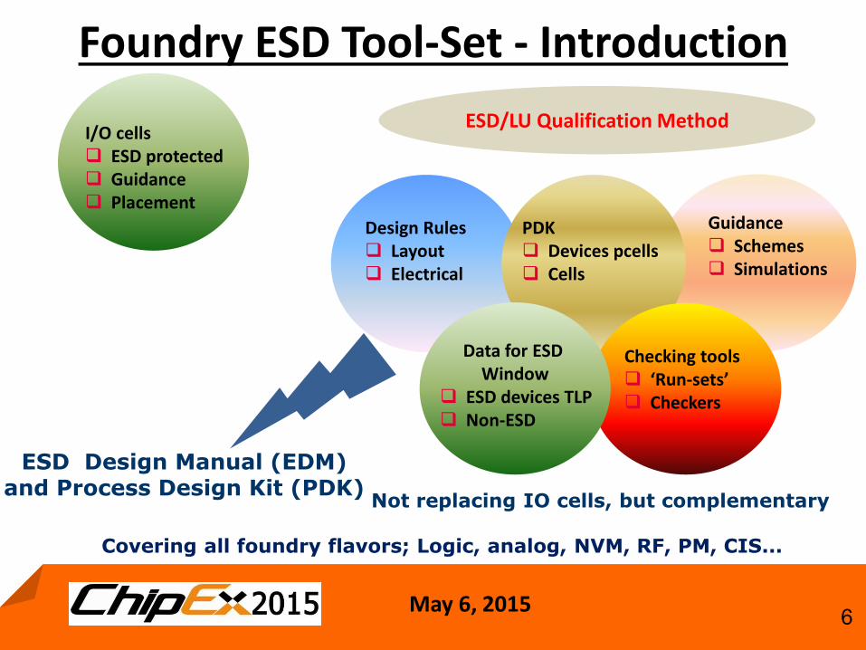
May 6, 2015 6
Guidance Schemes Simulations
Introduction -Set -Foundry ESD Tool
Design Rules Layout Electrical
PDK Devices pcells Cells
Checking tools ‘Run-sets’ Checkers
Data for ESD Window
ESD devices TLP Non-ESD
I/O cells ESD protected Guidance Placement
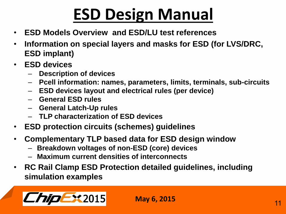
ESD Design Manual (EDM) and Process Design Kit (PDK)
Not replacing IO cells, but complementary
Covering all foundry flavors; Logic, analog, NVM, RF, PM, CIS...
ESD/LU Qualification Method
May 6, 2015 7
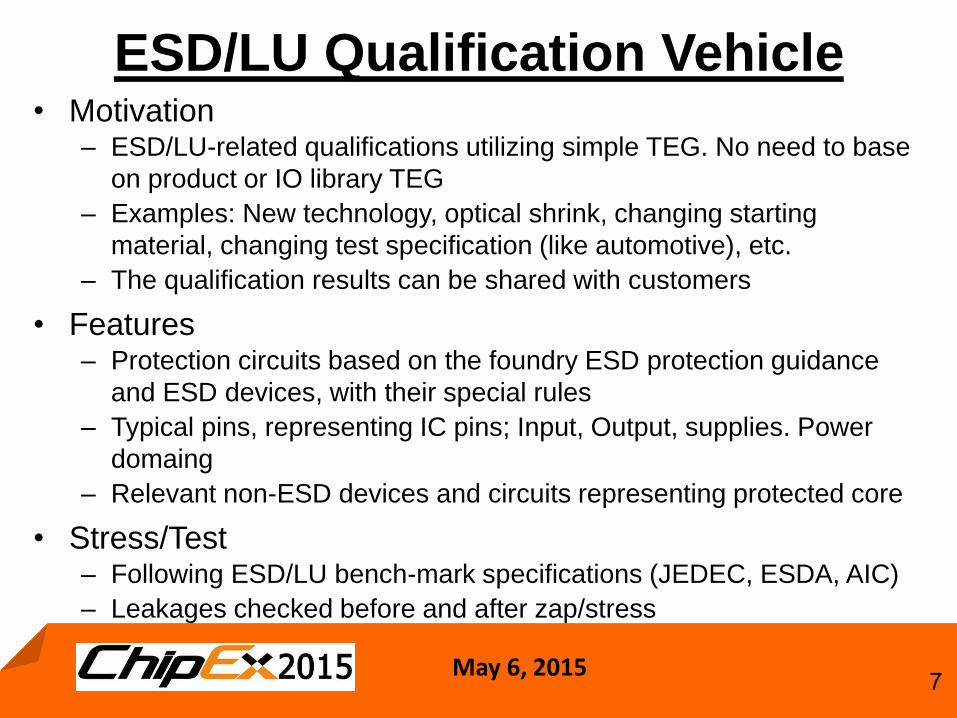
ualification VehicleESD/LU Q • Motivation
– ESD/LU-related qualifications utilizing simple TEG. No need to base
on product or IO library TEG
– Examples: New technology, optical shrink, changing starting
material, changing test specification (like automotive), etc.
– The qualification results can be shared with customers
• Features – Protection circuits based on the foundry ESD protection guidance
and ESD devices, with their special rules
– Typical pins, representing IC pins; Input, Output, supplies. Power
domaing
– Relevant non-ESD devices and circuits representing protected core
• Stress/Test – Following ESD/LU bench-mark specifications (JEDEC, ESDA, AIC)
– Leakages checked before and after zap/stress
May 6, 2015 8
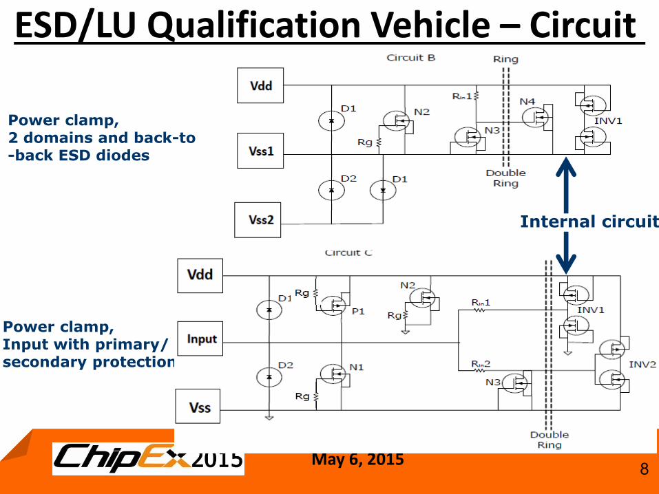
Circuit –ualification Vehicle QESD/LU Examples
Power clamp, 2 domains and back-to -back ESD diodes
Power clamp, Input with primary/ secondary protection
Internal circuit
May 6, 2015 9
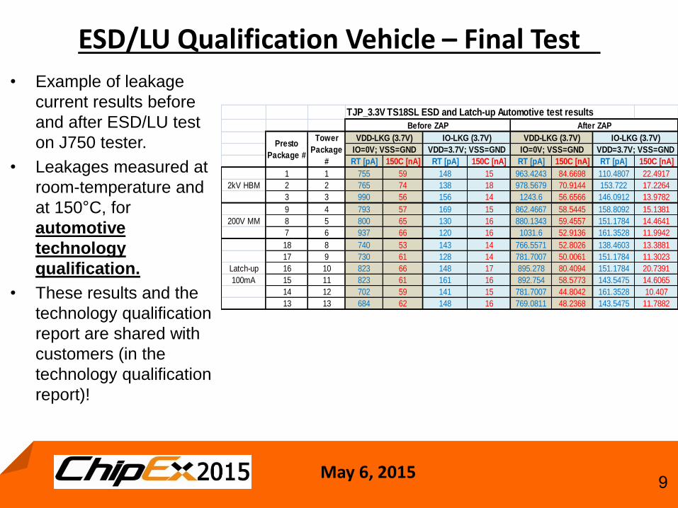
• Example of leakage
current results before
and after ESD/LU test
on J750 tester.
• Leakages measured at
room-temperature and
at 150°C, for
automotive
technology
qualification.
• These results and the
technology qualification
report are shared with
customers (in the
technology qualification
report)!
Final Test –ualification Vehicle QESD/LU
TJP_3.3V TS18SL ESD and Latch-up Automotive test results
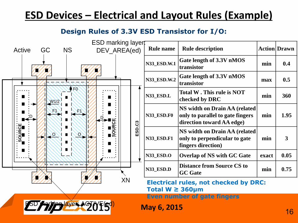
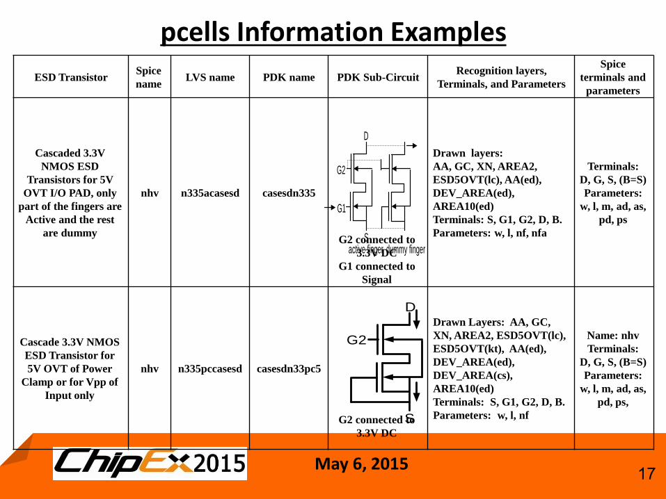
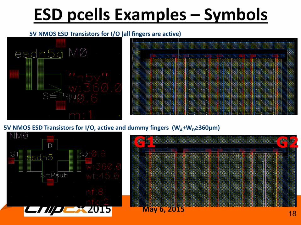
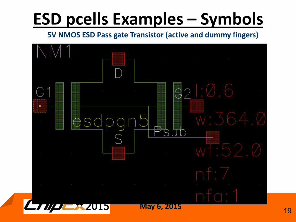
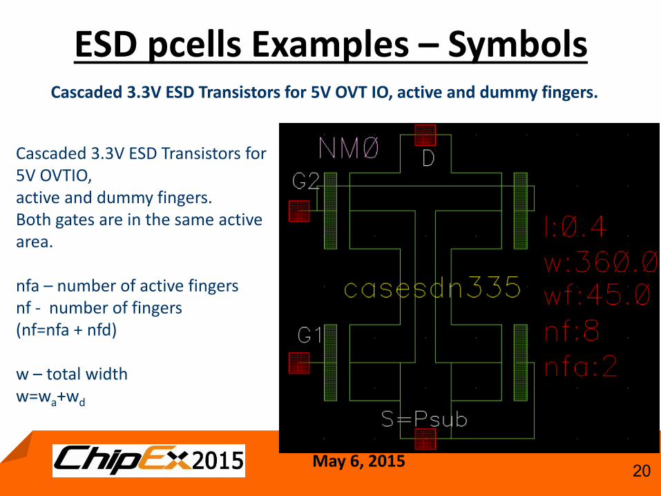
Cascaded 3.3V ESD Transistors for 5V OVTIO, active and dummy fingers. Both gates are in the same active area. nfa – number of active fingers nf - number of fingers (nf=nfa + nfd) w – total width w=wa+wd
Cascaded 3.3V ESD Transistors for 5V OVT IO, active and dummy fingers.
May 6, 2015 21
GUI Example pcellESD
Page 21
nfa – number of active fingers nf - number of fingers (nf=nfa + nfd)
w – total width w=wa+wd
Prevents electrical rule violation (W<min is not aloud, parameters out of limits not aloud, default parameters)
Actual average diffusion dimensions (area, perimeter) are calculated based on device parameter (finger width, number of fingers) Extracted and used in SPICE model
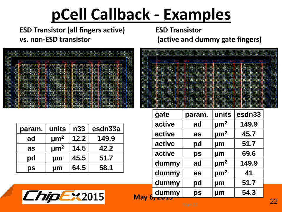
May 6, 2015 22
Examples -Callback pCell
Page 22
param. units n33 esdn33a
ad µm2 12.2 149.9
as µm2 14.5 42.2
pd µm 45.5 51.7
ps µm 64.5 58.1
gate param. units esdn33
active ad µm2 149.9
active as µm2 45.7
active pd µm 51.7
active ps µm 69.6
dummy ad µm2 149.9
dummy as µm2 41
dummy pd µm 51.7
dummy ps µm 54.3
ESD Transistor (all fingers active) vs. non-ESD transistor
ESD Transistor (active and dummy gate fingers)
May 6, 2015 23
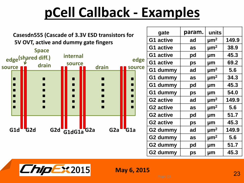
Examples -Callback pCell
Page 23
G1d G2d G2d G1d G1a G2a G2a G1a
drain drain edge
source
internal source
edge source
Space (shared diff.)
gate param. units
G1 active ad µm2 149.9
G1 active as µm2 38.9
G1 active pd µm 45.3
G1 active ps µm 69.2
G1 dummy ad µm2 5.6
G1 dummy as µm2 34.3
G1 dummy pd µm 45.3
G1 dummy ps µm 54.0
G2 active ad µm2 149.9
G2 active as µm2 5.6
G2 active pd µm 51.7
G2 active ps µm 45.3
G2 dummy ad µm2 149.9
G2 dummy as µm2 5.6
G2 dummy pd µm 51.7
G2 dummy ps µm 45.3
Casesdn555 (Cascade of 3.3V ESD transistors for 5V OVT, active and dummy gate fingers
May 6, 2015 24
Schemes –ESD Protection Circuit Guidance
• Design guidance for both normal operation and
ESD protection
• Output (self-protected)
• Input or I/O (bidirectional input/output)
– All gate fingers active
– Active and dummy gate fingers
– Negative input
• Power Clamp
• Over-Voltage-Tolerant pins; input, I/O, power
clamp
• Full IC; I/O ring, busses, multiple domains
May 6, 2015 25
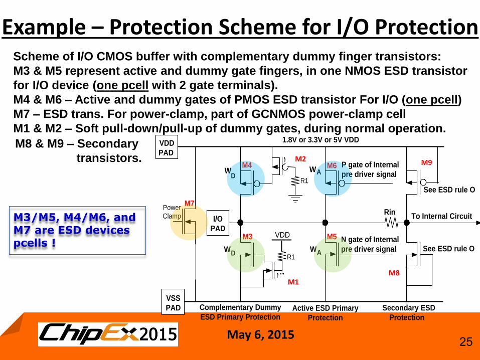
Protection Scheme for I/O Protection –Example
WD
WD
WA
WA
N gate of Internal
pre driver signal
Rin
P gate of Internal
pre driver signal
To Internal Circuit
See ESD rule O
See ESD rule O
VDD
R1
M2
VSS
PADVSS
PAD
R1
M1
Complementary Dummy
ESD Primary ProtectionActive ESD Primary
Protection
Secondary ESD
Protection
1.8V or 3.3V or 5V VDD
M4
M3 M5
M6
VDD
PAD
I/O
PAD
M7Power
Clamp
Only M3, M4 M5,
M6 and M7 are
ESD devices.
M1
M2 M9
M8
Scheme of I/O CMOS buffer with complementary dummy finger transistors:
M3 & M5 represent active and dummy gate fingers, in one NMOS ESD transistor
for I/O device (one pcell with 2 gate terminals).
M4 & M6 – Active and dummy gates of PMOS ESD transistor For I/O (one pcell)
M7 – ESD trans. For power-clamp, part of GCNMOS power-clamp cell
M1 & M2 – Soft pull-down/pull-up of dummy gates, during normal operation.
M8 & M9 – Secondary
transistors.
M3/M5, M4/M6, and M7 are ESD devices pcells !
May 6, 2015 26
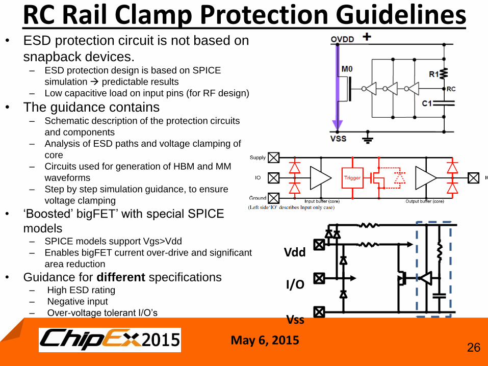
RC Rail Clamp Protection Guidelines • ESD protection circuit is not based on
snapback devices. – ESD protection design is based on SPICE
simulation predictable results
– Low capacitive load on input pins (for RF design)
• The guidance contains – Schematic description of the protection circuits
and components
– Analysis of ESD paths and voltage clamping of
core
– Circuits used for generation of HBM and MM
waveforms
– Step by step simulation guidance, to ensure
voltage clamping
• ‘Boosted’ bigFET’ with special SPICE
models – SPICE models support Vgs>Vdd
– Enables bigFET current over-drive and significant
area reduction
• Guidance for different specifications – High ESD rating
– Negative input
– Over-voltage tolerant I/O’s
Vdd
Vss
I/O
May 6, 2015 27
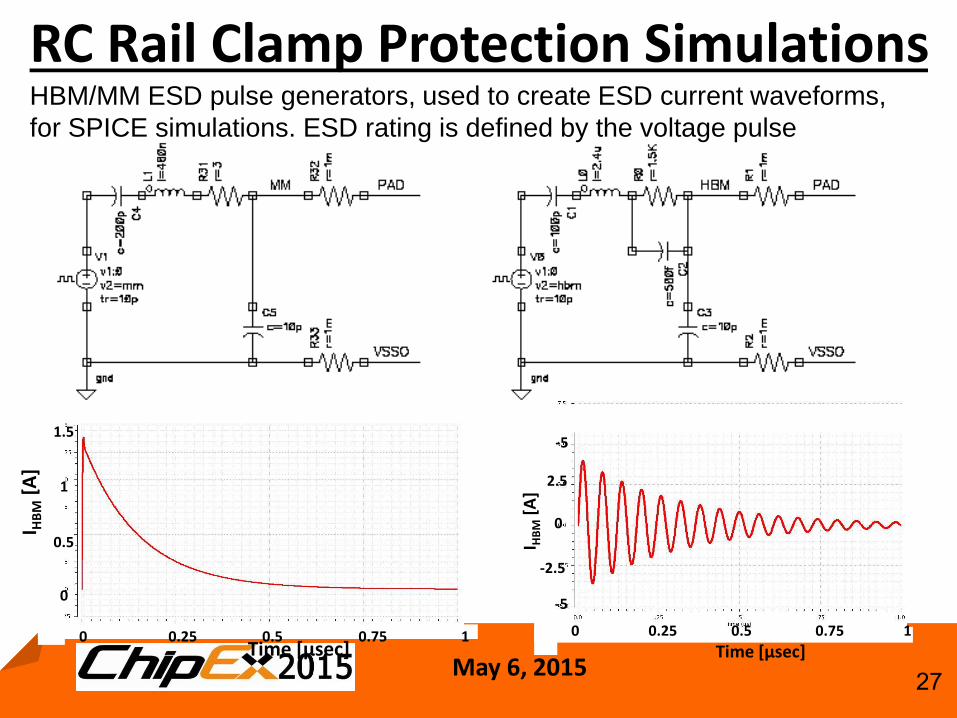
RC Rail Clamp Protection Simulations HBM/MM ESD pulse generators, used to create ESD current waveforms,
for SPICE simulations. ESD rating is defined by the voltage pulse
TT Time [µsec]
0 0.25 0.5 0.75 1
TT
-5
-2.5
0 I H
BM
[A
]
2.5
-5
TT
TT Time [µsec]
TT I
HB
M [
A]
0 0.25 0.5 0.75 1
0
0.5
1
1.5
May 6, 2015 28
RC Rail Clamp Simulation Guidelines
Page 28
May 6, 2015 29
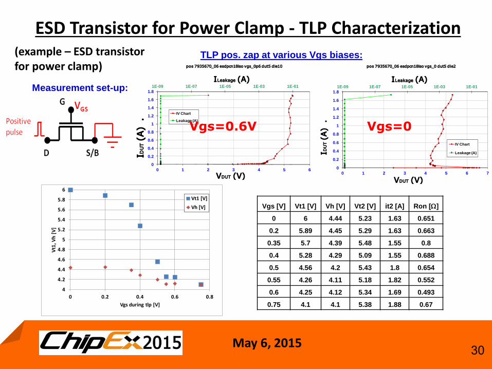
ESD Characterization
– Ensure ESD protection device off and no
Latch-Up risk during IC normal operation
– Ensure conductance of ESD current and
voltage clamping of protected circuit,
during the ESD event (both polarities)
• Type of data
– ESD characterization is based on
Transmission Line Pulse (TLP)
measurements
– DC I-V to check leakage at normal
operation
• Required characterization
– Critical parameters of ESD devices
(Vt1/Von, Vh, Vt2, it2, Ron)
– Breakdown voltages of non-ESD devices
(to be protected)
– Max ESD current densities and resistances
of interconnects (to carry the ESD current)
ESD characterization data is required for appropriate ESD protection
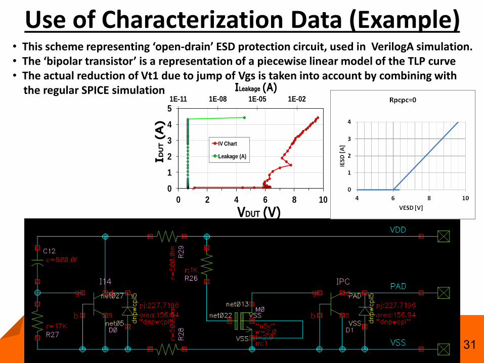
• This scheme representing ‘open-drain’ ESD protection circuit, used in VerilogA simulation. • The ‘bipolar transistor’ is a representation of a piecewise linear model of the TLP curve • The actual reduction of Vt1 due to jump of Vgs is taken into account by combining with the regular SPICE simulation
1E-11 1E-08 1E-05 1E-02
0
1
2
3
4
5
0 2 4 6 8 10
ILeakage (A)
ID
UT(A
)
VDUT (V)
IV Chart
Leakage (A)
May 6, 2015 32
Use of Characterization Data (Example)
Page 32
2KV HBM – VDD to PAD
May 6, 2015 33
Use of Characterization Data (Example)
Page 33
MM – VDD to Vss
May 6, 2015 34
ESD CHECKERS
Page 34
May 6, 2015 35
Overview -ESD Checking
Page 35
• Automatic verification of ESD robustness of Integrated Circuits is an
emerging part of the design review procedure and design flow
• DRC is layout-based (and not scheme-based), can be used only close to
tape-out, and does not verify ESD path
• Existing and developed checks can be categorized as either Design-Rule
check or Robustness check;
Item Check Challenge/Comment PDK benefit
ESD dedicated layout rules
DRC (Design Rule Check) Accurate layers placement (some for DRC purpose only)
Pcells are ‘DRC clean’
ESD electronic rules ERC (Electronic Rule Check)
Need to ‘translate’ guidelines and schemes to code
Pcells are ‘ERC clean’
ESD path verification Existence of ESD path Recognition of ESD devices Simple identification of ESD devices
Voltage Clamping Static Dynamic
ESD device modeling? Dynamic check ? Huge data-base is required
TLP characterization
Current density, along ESD path
Point to point Used also for EM robustness check
TLP characterization (of interconnects)
May 6, 2015 36
Approaches of Implementing PERC in TowerJazz*
Pre layout
• Topological checking with schematic
Post layout
• Schematic info. driven geometrical check
Implement key items from design rules and ESD design guidelines to PERC that traditional tools
cannot check automatically
Design rules manual
ESD design guidelines
May 6, 2015 37
PERC Implementation: ESD IO Rules Target:
Transistor connected directly by its drain to IO and source to power rail is considered as an ESD transistor and hence must comply with ESD design rules
May 6, 2015 38
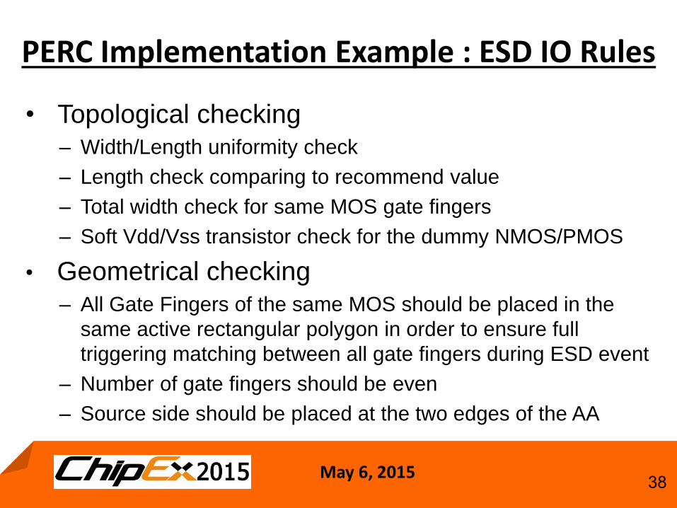
PERC Implementation Example : ESD IO Rules
• Topological checking
– Width/Length uniformity check
– Length check comparing to recommend value
– Total width check for same MOS gate fingers
– Soft Vdd/Vss transistor check for the dummy NMOS/PMOS
• Geometrical checking
– All Gate Fingers of the same MOS should be placed in the
same active rectangular polygon in order to ensure full
triggering matching between all gate fingers during ESD event
– Number of gate fingers should be even
– Source side should be placed at the two edges of the AA
May 6, 2015 39
Topological Checking Example of ESD IO Rules
Error detected due to “Missing soft Vdd transistor for the dummy NMOS”
May 6, 2015 40
ESD OFFERING FOR POWER MANAGEMENT PLATFORMS (JUST TASTE)
Page 40
May 6, 2015 41
ESD Challenge for Scalable Voltage Platforms
ESD Challenges: 1. Good Vdd Rdson Tradeoff (BVdss-ESD
design window = Vdd) 2. Scalable voltage platform Need
scalable ESD voltage solutions 3. Capability to tune ESD Rating. 4. Small footprint.
Curr
ent
Voltage
IC o
pe
ration
are
a
Thermal Failure Effect
Min
Bre
akdo
wn
/Rel.
Vo
lta
ge o
f IC
due
to
ES
D tra
nsie
nt
of
TL
P p
uls
e
(Vh, Ih)(Vt1, It1)
(Vt2, It2)
Safe ESD
protection
window
Sa
fety
ma
rgin
Safety
margin
Sa
fety
ma
rgin
Vdd
May 6, 2015 42
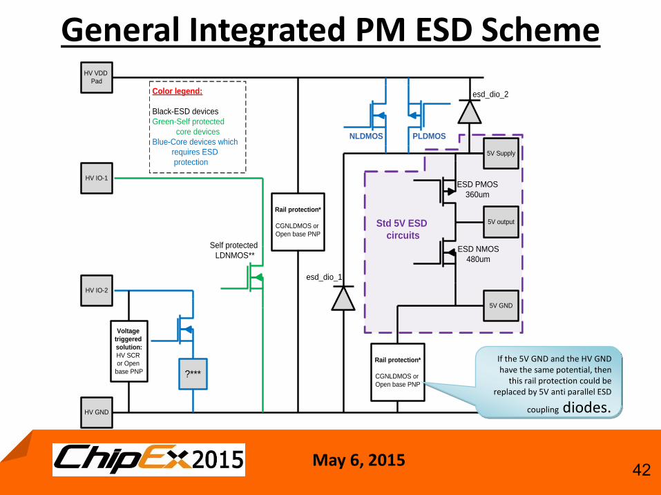
General Integrated PM ESD Scheme
5V Supply
HV VDD
Pad
HV GND
HV IO-1
?***
HV IO-2
Self protected
LDNMOS**
5V output
5V GND
esd_dio_2
ESD PMOS
360um
ESD NMOS
480um
PLDMOSNLDMOS
:Color legend
Black-ESD devices
Green-Self protected
core devices
Blue-Core devices which
requires ESD
protection
Std 5V ESD
circuits
Voltage
triggered
solution:
HV SCR
or Open
base PNP
Rail protection*
CGNLDMOS or
Open base PNP
Rail protection*
CGNLDMOS or
Open base PNP
esd_dio_1
If the 5V GND and the HV GND have the same potential, then
this rail protection could be replaced by 5V anti parallel ESD
probability of IC ESD protection safe time success.
• Based on long interaction with our customers and evaluation of designers needs, TowerJazz developed a long list of devices and protection schemes covering a wide range of IC pins and specifications.
• Automatic tools are continuously adopted for ESD Electronic rules check. TowerJazz implemented Calibre PERC and plans additional tools to cover other aspects of ESD protection verification.
• TowerJazz offers a full ESD coverage for PM platforms including: Scalable voltage ESD solutions Scalable ESD rating solutions Both RC coupled and voltage triggered solutions ESD pcells including ESD parameters calculators