9
FOUR WAYS TO IMPROVE THE SOLDERABILITY OF YOUR NEXT DESIGN

FOUR WAYS TO IMPROVE THE SOLDERABILITY OF
YOUR NEXT DESIGN
Pg. 2
TABLE OF CONTENTS
1. What is Solder Thieving?
2. The Problem
3. Solution #1
4. Solution #2
5. Solution #3
6. Solution #4
Pg. 3
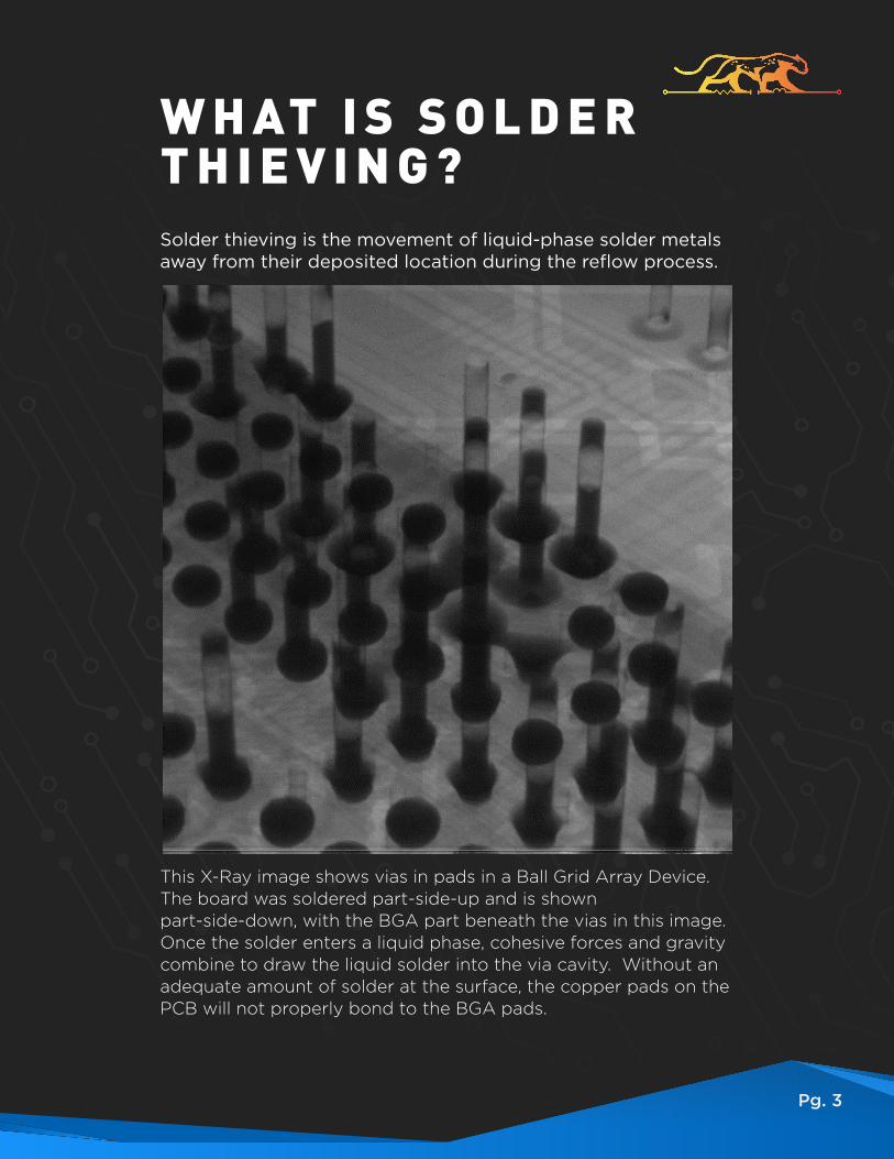
W H AT I S S O L D E R T H I E V I N G ?Solder thieving is the movement of liquid-phase solder metals away from their deposited location during the reflow process.
This X-Ray image shows vias in pads in a Ball Grid Array Device. The board was soldered part-side-up and is shown part-side-down, with the BGA part beneath the vias in this image. Once the solder enters a liquid phase, cohesive forces and gravity combine to draw the liquid solder into the via cavity. Without an adequate amount of solder at the surface, the copper pads on the PCB will not properly bond to the BGA pads.
Pg. 4
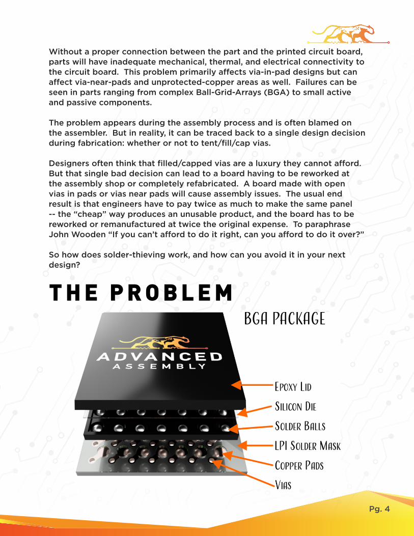
Without a proper connection between the part and the printed circuit board, parts will have inadequate mechanical, thermal, and electrical connectivity to the circuit board. This problem primarily affects via-in-pad designs but can affect via-near-pads and unprotected-copper areas as well. Failures can be seen in parts ranging from complex Ball-Grid-Arrays (BGA) to small active and passive components.
The problem appears during the assembly process and is often blamed on the assembler. But in reality, it can be traced back to a single design decision during fabrication: whether or not to tent/fill/cap vias.
Designers often think that filled/capped vias are a luxury they cannot afford. But that single bad decision can lead to a board having to be reworked at the assembly shop or completely refabricated. A board made with open vias in pads or vias near pads will cause assembly issues. The usual end result is that engineers have to pay twice as much to make the same panel -- the “cheap” way produces an unusable product, and the board has to be reworked or remanufactured at twice the original expense. To paraphrase John Wooden “If you can’t afford to do it right, can you afford to do it over?”
So how does solder-thieving work, and how can you avoid it in your next design?
T H E P R O B L E M
Pg. 5
FOUR WAYS TO IMPROVE THE SOLDERABILITY OF YOUR NEXT DESIGN
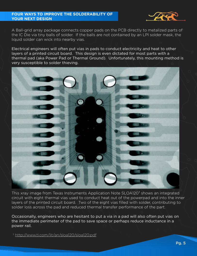
A Ball-grid array package connects copper pads on the PCB directly to metalized parts of the IC Die via tiny balls of solder. If the balls are not contained by an LPI solder mask, the liquid solder can wick into nearby vias.
Electrical engineers will often put vias in pads to conduct electricity and heat to other layers of a printed circuit board. This design is even dictated for most parts with a thermal pad (aka Power Pad or Thermal Ground). Unfortunately, this mounting method is very susceptible to solder thieving.
This xray image from Texas Instruments Application Note SLOA120¹¹ shows an integrated circuit with eight thermal vias used to conduct heat out of the powerpad and into the inner layers of the printed circuit board. Two of the eight vias filled with solder, contributing to solder loss across the pad and reduced thermal transfer performance of the part.
Occasionally, engineers who are hesitant to put a via in a pad will also often put vias on the immediate perimeter of the pad to save space or perhaps reduce inductance in a power rail.
1 http://www.ti.com/lit/an/sloa120/sloa120.pdf
Pg. 6
FOUR WAYS TO IMPROVE THE SOLDERABILITY OF YOUR NEXT DESIGN
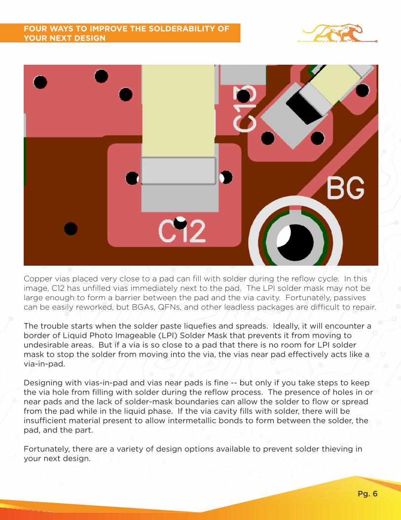
Copper vias placed very close to a pad can fill with solder during the reflow cycle. In this image, C12 has unfilled vias immediately next to the pad. The LPI solder mask may not be large enough to form a barrier between the pad and the via cavity. Fortunately, passives can be easily reworked, but BGAs, QFNs, and other leadless packages are difficult to repair.
The trouble starts when the solder paste liquefies and spreads. Ideally, it will encounter a border of Liquid Photo Imageable (LPI) Solder Mask that prevents it from moving to undesirable areas. But if a via is so close to a pad that there is no room for LPI solder mask to stop the solder from moving into the via, the vias near pad effectively acts like a via-in-pad.
Designing with vias-in-pad and vias near pads is fine -- but only if you take steps to keep the via hole from filling with solder during the reflow process. The presence of holes in or near pads and the lack of solder-mask boundaries can allow the solder to flow or spread from the pad while in the liquid phase. If the via cavity fills with solder, there will be insufficient material present to allow intermetallic bonds to form between the solder, the pad, and the part.
Fortunately, there are a variety of design options available to prevent solder thieving in your next design.
Pg. 7
FOUR WAYS TO IMPROVE THE SOLDERABILITY OF YOUR NEXT DESIGN
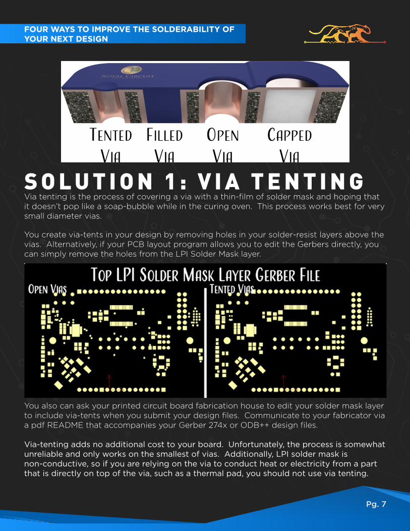
S O L U T I O N 1 : V I A T E N T I N GVia tenting is the process of covering a via with a thin-film of solder mask and hoping that it doesn’t pop like a soap-bubble while in the curing oven. This process works best for very small diameter vias.
You create via-tents in your design by removing holes in your solder-resist layers above the vias. Alternatively, if your PCB layout program allows you to edit the Gerbers directly, you can simply remove the holes from the LPI Solder Mask layer.
You also can ask your printed circuit board fabrication house to edit your solder mask layer to include via-tents when you submit your design files. Communicate to your fabricator via a pdf README that accompanies your Gerber 274x or ODB++ design files.
Via-tenting adds no additional cost to your board. Unfortunately, the process is somewhat unreliable and only works on the smallest of vias. Additionally, LPI solder mask is non-conductive, so if you are relying on the via to conduct heat or electricity from a part that is directly on top of the via, such as a thermal pad, you should not use via tenting.
Pg. 8
S O L U T I O N N O N -C O N D U C T I V E V I A F I L L I N GThe least-expensive fill material to fill a via hole is Liquid Photo Imageable (LPI) solder resist. Fabricators force solder-resist into the via holes and then cure it in a high-temperature oven. LPI Solder resist is obviously non-conductive, but unless you have a high-current or high-heat application, it shouldn’t really matter. The material that was in your via before the solder mask was air, which is a horrible conductor of heat and electricity. The LPI solder resist provides a marginal improvement over air.
This method is useful when vias are very near a copper pad. Unlike via-tenting, this technique will work 100% of the time. You can also use this technique in situations where the via is much smaller than the pad -- such as thermal pads.
Remember that the copper on the via walls will still be present and can transfer a great deal of heat and electricity between layers. If you need a modest increase in thermal or electrical performance, just increase the number of vias, the plating thickness, or the trace width of layers above and below the via.In his book “PCB Trace and Via Currents and Temperatures, The Complete Analysis, 2nd Edition” Douglas Brooks, Ph.D. notes that “the current does not determine the via temperature, the trace has much more influence over the via
temperature.” The limited research in the area of via current-carrying capacity has led to very conservative estimates of via performance. The deprecated IPC-2221 guidelines, the current IPC-2152 guidelines, and conventional wisdom all suggest using a via with approximately the same cross-sectional area as the trace it connects to. But this doesn’t take into account the conductive cooling offered by the dielectric material. So, from a thermal management standpoint, you can often design a via with a cross-sectional area that is less than the cross-sectional area of the trace. Plating thickness is not always consistent, so you might consider increasing your plating thickness or using multiple vias to connect traces between layers before you invest in filling your vias with conductive epoxy.
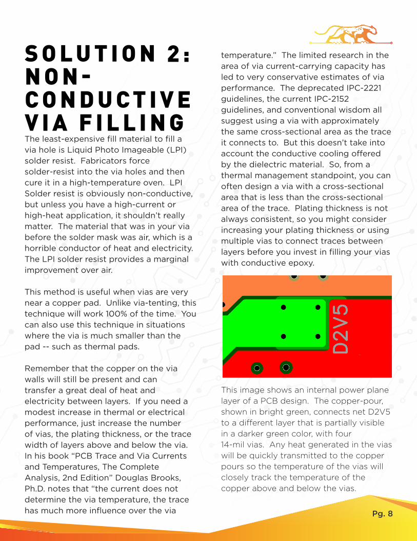
This image shows an internal power plane layer of a PCB design. The copper-pour, shown in bright green, connects net D2V5 to a different layer that is partially visible in a darker green color, with four 14-mil vias. Any heat generated in the vias will be quickly transmitted to the copper pours so the temperature of the vias will closely track the temperature of the copper above and below the vias.
2 :
Pg. 9
FOUR WAYS TO IMPROVE THE SOLDERABILITY OF YOUR NEXT DESIGN
S O L U T I O N 3 : V I A C A P P I N GAfter your via is filled, fabricators can then sand your board and put it back in the electroplating tanks. This covers the capped via with a layer of plated copper. At this point, the via is completely full of material and enclosed at either end by copper pads. Via capping is necessary for via-in-pad designs. Later in the manufacturing stages, parts can be soldered directly to the pads.
S O L U T I O N 4 : C O N D U C T I V E V I A - F I L L I N GConductive ExpoxiesConductive via-fill uses epoxies full of silver or copper particles that are forced into via holes after the via walls have been formed. The metal particles increase the thermal conductivity of the via, making this process important for high-current and high-heat traces. This technique is not often required in designs. As mentioned earlier -- via temperature is mostly coupled to the temperature of the traces.
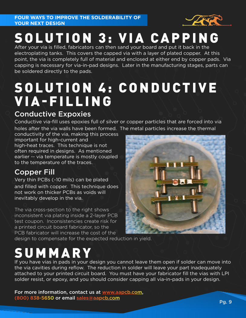
Copper FillVery thin PCBs (~10 mils) can be plated and filled with copper. This technique does not work on thicker PCBs as voids will inevitably develop in the via.
The via cross-section to the right shows inconsistent via plating inside a 2-layer PCB test coupon. Inconsistencies create risk for a printed circuit board fabricator, so the PCB fabricator will increase the cost of the design to compensate for the expected reduction in yield.
S U M M A R YIf you have vias in pads in your design you cannot leave them open if solder can move into the via cavities during reflow. The reduction in solder will leave your part inadequately attached to your printed circuit board. You must have your fabricator fill the vias with LPI solder resist, or epoxy, and you should consider capping all via-in-pads in your design.
For more information, contact us at www.aapcb.com, (800) 838-5650 or email [email protected]


