14
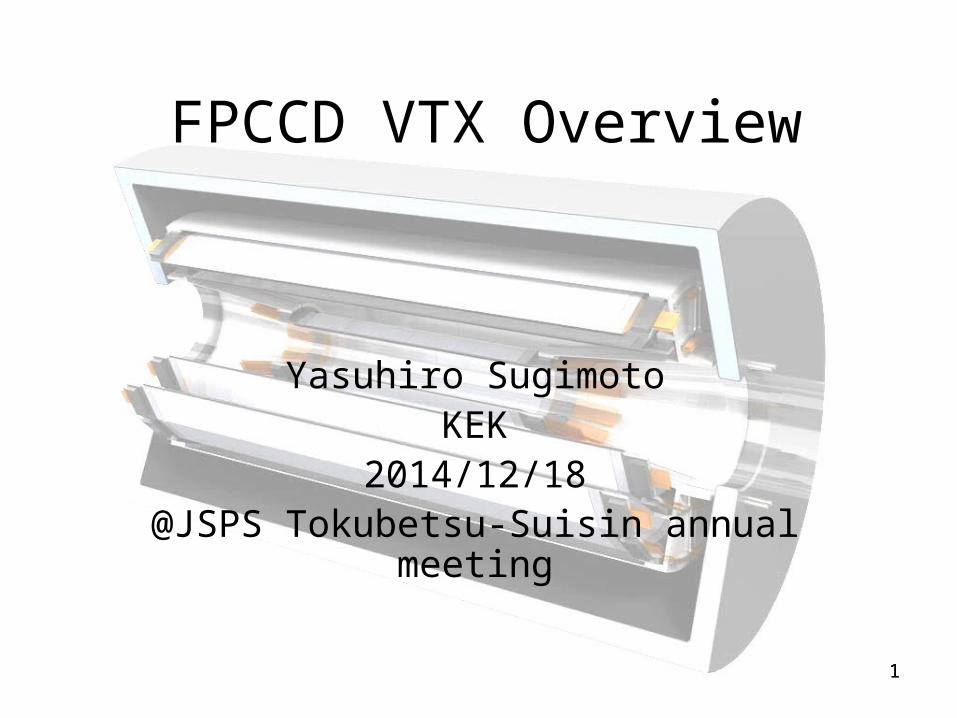
FPCCD VTX Overview Yasuhiro Sugimoto KEK 2014/12/18 @JSPS Tokubetsu-Suisin annual meeting 1
| Date post: | 14-Dec-2015 |
| Category: |
Documents |
| Upload: | antony-matthews |
| View: | 214 times |
| Download: | 1 times |
FPCCD VTX Overview
Yasuhiro SugimotoKEK
2014/12/18@JSPS Tokubetsu-Suisin annual meeting
11
Outline
• FPCCD sensor R&D
• Beam test
• Readout electronics
• CO2 cooling
• FY2015 plan
2

Vertex detector for ILD• Structure
– Barrel part only: |z|=62.5/125 mm– Double-sided layer x3– R=16~60mm– |cos|<0.97
• Minimization of material budget of ladders is a big challenge– 0.3%X0/ladder = 0.15%X0/layer
3

FPCCD sensor R&DFY Senor
2004 Fully depleted CCD, 24um pixel
2005 Fully depleted CCD, 24um pixel
2006 Fully depleted CCD, 24um pixel
2007 1st FPCCD: small size (6mm2),12um pixel
2008 2nd FPCCD: small size, 12um pixel (modified output amp)
2009 3rd FPCCD: small size, 12, 9.6, 8, 6um pixel
2010 4th FPCCD: small size, 12, 9.6, 8, 6um pixel (modified process)
Thin wafer:50um
2011 Small size, 12, 9.6, 8, 6um pixel (modified process), thin wafer
2012 Small size, 6um pixel, 4ch, different H-register size, high-R 15um epi
Large size (12x64mm2), 6,8,12um pixel, 8ch, high-R 15um epi
Small size, 6um pixel, thin wafer (for beam test), high-R 15um epi
2013 Small size, 6um pixel, high-R 15um epi4

FPCCD sensor R&D
• Original plan for sensor R&D in FY2014– Small size 5um pixel
• Achievement– It was found that developing 5um pixel CCD is
difficult for HPK• Too big technical challenge which requires cost and
manpower
– Packaged prototypes with mixed size pixel (12, 9.6, 8, 6 um) and high-R 15um epi: Same format as FY2011 small prototype but with different epitaxial layer
5

FPCCD sensor R&D
• Test of sensors using beta/X-ray source– Systematic study of FPCCD property is
mandatory• Dark current as a function of temperature / pixel-
size / irradiation• Energy resolution for 5.9 keV X-ray• Charge transfer inefficiency as a function of
various parameters• etc.
– Some of the achievements will be reported by Tino and Ito-san
6

Beam test
• Neutron damage test at CYRIC– Two CCD sample were irradiated by neutron beam at
CYRIC of Tohoku University– Detail will be reported by Ishikawa-san and Ito-san
• MIP beam test with ~1 GeV/c pion at J-PARC has not been done because the hadron-hall is not available yet
• Design of electron test beam line at KEK AR (South experimental hall) up to ~4.5 GeV is being carried out
7

Readout electronics
• Development of new clock driver and interface board– 3-level clock to reduce power consumption– Interface board for the new clock drivers– Detail will be reported later
8

Cooling system for VTX
• R&D of 2-phase CO2 cooling is being carried out for FPCCD VTX (and TPC) using another funding
• A prototype of circulating cooling system using a gas compressor has been constructed– Cooling temperature: between −40℃ and +15℃– The system has been tested, and we
demonstrated that it can achieve the design cooling temperature
9

Cooling system for VTX
• Prototype of 2-phase CO2 cooling system
10
Cooling line at -40 ℃

FY2015 plan (tentative)• FPCCD sensors
– Small prototypes with same format as before– Systematic study of FPCCD property should be continued
• Ladder R&D– Mechanical ladder structure
• Original idea: Carbon foam (RVC) core sandwiched by CFRP sheets Risk of carbon powder
• All CFRP structure seems better
• Electronics R&D– Readout speed of 10Mpix/s
• So far, stable readout of 2.5Mpix/s (25MHz clock) has been achieved• Our goal is 10Mpix/s• We have to find out the problem, and make improved readout system
– Bare chip test board with similar structure to ladder• CFRP base + Kapton FPC + bare chips
11

Backup slides
12

R&D goal
• FPCCD sensors– Pixel size; 6um– Chip size;1cmx6.5cm– Speed >10Mpix/s– F.W.C. > 10000 e(?)– Power <10mW/ch– Rad. Tolerance >1x10¹³e/cm2
(=1x10¹²/cm2/y x 3y x safety factor 3)
• Readout ASIC– Speed > 10Mpix/s– Power < 6mW/ch– Noise < 30 electrons
• Peripheral circuit– Clock driver– Data suppression– Etc.
• Engineering R&D– Over-all design– Low-mass ladder– Cooling system (~-40℃)– Support structure Engineering prototype
13
5um (?)

Ladder
• Structure
Layer-1 Layer-2,314


