Page 1
© 2015, IJCERT All Rights Reserved Page | 1076
International Journal of Computer Engineering In Research Trends
Volume 2, Issue 12, December-2015, pp. 1076-1082 ISSN (O): 2349-7084
FPGA Based Efficient Implementation of Viterbi Decoder
1BEERAM RAJ MOHAN REDDY, 2 BELLAM VARALAKSHMI 1(M.Tech) VLSI, Dept. of ECE
2Assistant Professor, Dept. of ECE
Priyadarshini Institute of Technology & Management Abstract:- Convolutional encoding is a forward error correction technique that is used for correction of errors at the
receiver end. The Viterbi algorithm, which is the most extensively employed decoding algorithm for convolutional codes. In this paper, we present a Spartan XC3S400A Field- Programmable Gate Array efficient implementation of Viterbi Decoder with a constraint length of 3 and a code rate of 1/3. The proposed architecture can be realized by an Adaptive Viterbi Decoder having constraint length, K of 3 and a code rate (k/n) of 1/2 using Verilog HDL. Simulation is done using Xilinx ISE 12.4i design software and it is targeted into Xilinx Virtex-5, XC5VLX110T FPGA. The parameters of Viterbi algorithm can be changed to suit a specific application. The high speed and small area are two important design parameters in today’s wireless technology. In this paper, a high speed feed forward viterbi decoder has been designed using track back architecture and embedded BRAM of target FPGA. It shows that the larger the constraint length used in a convolutional encoding process, the more powerful the code produced.
Keywords – Convolutional encoding, Viterbi decoder, Path Metric, branch metric, FPGA, Xilinx, Modelsim.
1. INTRODUCTION
In digital communication system, error detection and
error correction is important for reliable
communication. Error detection techniques are much
simpler than forward error correction (FEC).But error
detection techniques have certain disadvantages.
Error detection pre supposes the existence of an
automatic repeat request (ARQ)[1] feature which
provides for the retransmission of those blocks,
segments or packets in which errors have been
detected. With the growing use of digital
communication, there has been an increased interest
in high-speed Viterbi decoder design within a single
chip. The Convolutional encoder adds redundancy to
a continuous stream of input data by using a linear
shift register. Adaptive Viterbi decoder is very
efficient and robust. The main advantage of Adaptive
Viterbi Decoder is it has fixed decoding time and also
it suites for hardware decoding implementation. The
implementation requires the exponential increase in
the area and power consumption to achieve increased
decoding accuracy.The Viterbi algorithm essentially
performs maximum likelihood decoding to correct the
errors in received data which are caused by the
channel noise; however it reduces the computational
load by taking advantage of special structure in the
code trellis [2]. The Viterbi algorithm (VA) is a
recursive optimal solution to the problem of
estimating the state sequence of a discrete time finite
state Markov process. Viterbi decoding has the
advantage that it has a fixed decoding time and it is
well suited to hardware decoder implementation. The
requirements for the Viterbi decoder, which is a
processor that implements the Viterbi algorithm,
depend on the application in which it is used. The
Virtex-II family is a platform FPGA developed for
high performance from low-density to high-density
designs which are optimized for high speed with low
power consumption. The device XC2V2000 of this
family can excellently meet the performance and
Available online at: www.ijcert.org
Page 2
Mohan Reddy et al., International Journal of Computer Engineering In Research Trends Volume 2, Issue 12, December-2015, pp. 1076-1082
© 2015, IJCERT All Rights Reserved Page | 1077
stability requirements of the encoder and decoder
according to the experiments.
The designs are described using Verilog HDL[3] for
the hard-ware implementation on the above FPGA
and it can be configurable. In such cases, for ward
error correction, in addition to error detection with
ARQ, may considerably improve throughput.
Forward error correction may be desirable in place of,
or in addition to, error detection for any of the
following reasons:
I. When a reverse channel is not available or the delay
with ARQ would be excessive.
II. There transmission strategy is not conveniently
implemented.
Keeping in view requirements of communication
channels in 3G wireless systems, need of reliable data
communication, fast as well as accurate is the main
consideration.
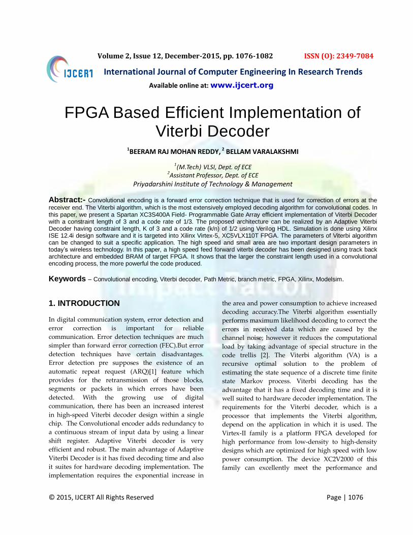
2. Viterbi Decoder A viterbi decoder uses the Viterbi algorithm for
decoding a bitstream that has been encoded using
Forward error correction based on a code. A structure
and short overview of the basic Viterbi decoding
system is illustrated in Fig. 1. This figure shows three
basic elements of the Viterbi decoding communication
system: convolutional encoder, communication
channel and Viterbi decoder.
Fig 1: Block diagram of Viterbi decoder
When a sequence of data is received from the channel,
it is required to estimate the original sequence that has
been sent. The process of identifying original message
sequence from the received data can be done using the
diagram called "trellis".
The Viterbi Decoder consists of following functional
parts
a). Branch Metric Unit (BMU)
b). Add Compare Select Unit (ACSU)
c). Survivor Memory Management Unit (SMU).
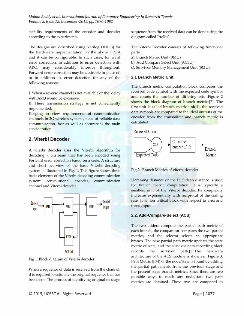
2.1 Branch Metric Unit:
The branch metric computation block compares the
received code symbol with the expected code symbol
and counts the number of differing bits .Figure 2
shows the block diagram of branch metrics[7]. The
first unit is called branch metric unit[4], the received
data symbols are compared to the ideal outputs of the
encoder from the transmitter and branch metric is
calculated.
Fig 2: Branch Metrics of viterbi decoder
Hamming distance or the Euclidean distance is used
for branch metric computation. It is typically a
smallest unit of the Viterbi decoder. Its complexity
increases exponentially with reciprocal of the coding
rate. It is non critical block with respect to area and
throughput.
2.2. Add-Compare-Select (ACS)
The two adders compute the partial path metric of
each branch, the comparator compares the two partial
metrics, and the selector selects an appropriate
branch. The new partial path metric updates the state
metric of state, and the survivor path-recording block
records the survivor path.[5].The hardware
architecture of the ACS module is shown in Figure 3.
Path Metric (PM) of the node/state is found by adding
the partial path metric from the previous stage and
the present stage branch metrics. Since there are two
possible ways to reach any node/state two path
metrics are obtained. These two are compared to
Page 3
Mohan Reddy et al., International Journal of Computer Engineering In Research Trends Volume 2, Issue 12, December-2015, pp. 1076-1082
© 2015, IJCERT All Rights Reserved Page | 1078
select the one with the least path metric. The path
with the better metric is chosen and stored as the new
path metric for current state, while generating a
decision bit.
The decision bit indicates what branch was chosen.
Because each state can be achieved from the earlier
stage, the decision value is represented by one bit. If
the bit is „1‟ the path selected is coming from the
lower state from those two possible states in the trellis
diagram, and if the decision bit is „0‟ the path
selected is coming from the upper state. As the ACS
unit needs the results from the calculations of the
previous steps, it forms a feedback loop with the path
metric memory unit, where the results are stored.
Fig 3: ACS (Add Compare select) module
2.3 Survivour Memory Management Unit
The final unit is the trace-back process or register
exchange method, where the survivor path and the
output data are identified. The trace-back (TB)[6] and
the register exchange (RE) methods are the two major
techniques used for the path history management in
the chip designs of Viterbi decoders. The TB method
takes up less area but requires more time as compared
to RE method because it needs to search or trace the
survivor path back sequentially. Also, extra hardware
is required to reverse the decoded bits.
The Survivor Memory management Unit (SMU)
[7]stores the decisions of the ACS unit and uses them
to compute the decoded output. The Trace-Back (TB)
technique and the Register-Exchange (RE) approaches
are two major techniques used for the path history
management .The Trace Back unit takes up less area
but require much more time than the Register
Exchange method.
A relatively new approach called Permutation
Network based Path History (PNPH) [8]unit
implements directly the trellis diagram of the given
Convolution code to trace the survivor path back
sequentially. The resulting circuit has smaller routing
area than register-exchange technique and has faster
decoding speed than trace-back method regardless of
the constraint length.
Permutation network based path history (PNPH) unit:
The Permutation Network based Path History (PNPH)
unit for an convolutional code is a 5L-stage
permutation network with each stage containing 1-to-
2k demultiplexers, where each Demux corresponds to
each node of the trellis diagram and is associated with
a K-bit register and a 2k-input OR gate. The K bit
register is used to store the decision bits associated
with the state node and to determine the partial
survivor path associated with the node. Thus, each
registers demultiplexer pair determines the part of the
survivor path associated its corresponding state node.
3. PROGRAMMABLE DEVICES Programmable devices are those devices which can be
programmed by the user. Various programmable
devices are PLDs, CPLDs, ASICs and FPGAs [9].
3.1 Field Programmable Gate Arrays
'Field Programmable' means that the FPGA's function
is defined by a user's program rather than by the
manufacturer of the device. A Field Programmable
Gate Array (FPGA) is a semiconductor device
containing programmable logic components and
programmable interconnects.
The programmable logic components can be
programmed to duplicate the functionality of basic
logic gates such as AND, OR, XOR, NOT or more
complex combinational functions such as decoders or
simple math functions.
FPGAs originally began as competitors to CPLDs and
competed in a similar space, that of glue logic for
Page 4
Mohan Reddy et al., International Journal of Computer Engineering In Research Trends Volume 2, Issue 12, December-2015, pp. 1076-1082
© 2015, IJCERT All Rights Reserved Page | 1079
PCBs. As their size, capabilities and speed increase,
they began to take over larger and larger functions to
the state where they are now market as competitors
for full systems on chips. They now find applications
in any area or algorithm that can make use of the
massive parallelism offered by their architecture. [10].
3.2 SPARTAN XC3S400A FPGA
The Spartan 3A family of Field-Programmable Gate
Arrays (FPGAs) solves the design challenges in most
high volume, cost-sensitive, I/O-intensive electronic
applications .Because of their exceptionally low cost,
Spartan-3A FPGAs are ideally suited to a wide range
of consumer electronics applications, including
broadband access, home networking,
display/projection, and digital television equipment. A
Xilinx Spartan-3A (XC3S400A- 4FTG256C) 400 K gate
FPGA and a Cypress Cy8C24894 PSoC Mixed-Signal
Array are the primary components of the Avnet
Spartan-3A evaluation board. In addition to onboard
processing functions, the PSoC device provides off
board communication via a USB 2.0 full-speed
interface.
4. VITERBI DECODER DESIGN AND IMPLEMENTATION 4.1 System block diagram
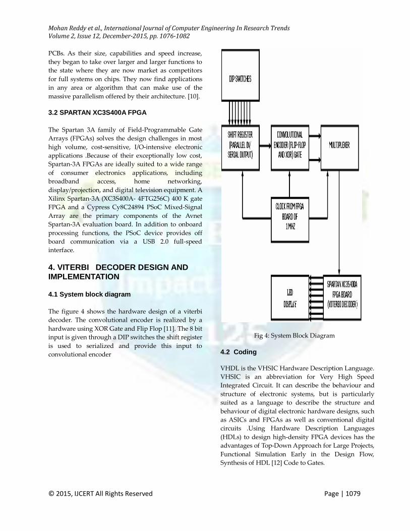
The figure 4 shows the hardware design of a viterbi
decoder. The convolutional encoder is realized by a
hardware using XOR Gate and Flip Flop [11]. The 8 bit
input is given through a DIP switches the shift register
is used to serialized and provide this input to
convolutional encoder
Fig 4: System Block Diagram
4.2 Coding
VHDL is the VHSIC Hardware Description Language.
VHSIC is an abbreviation for Very High Speed
Integrated Circuit. It can describe the behaviour and
structure of electronic systems, but is particularly
suited as a language to describe the structure and
behaviour of digital electronic hardware designs, such
as ASICs and FPGAs as well as conventional digital
circuits .Using Hardware Description Languages
(HDLs) to design high-density FPGA devices has the
advantages of Top-Down Approach for Large Projects,
Functional Simulation Early in the Design Flow,
Synthesis of HDL [12] Code to Gates.
Page 5
Mohan Reddy et al., International Journal of Computer Engineering In Research Trends Volume 2, Issue 12, December-2015, pp. 1076-1082
© 2015, IJCERT All Rights Reserved Page | 1080
4.3 Vietrbi decoder algorithm Design flow
The algorithm can be broken down into the following
three steps.
1. Weigh the trellis; that is, calculate the branch
metrics.
2. Recursively computes the shortest paths to time n,
in terms of the shortest paths to time n-1. In this step,
decisions are used to recursively update the survivor
path of the signal. This is known as add-compare
select
(ACS) recursion.
4.4 Design entry using Xilinx ISE 10.1 design Suite
In the design entry process, the behavior of circuit is
written in hardware description language like VHDL.
Simulation and synthesis are the two main kinds of
tools which operate on the VHDL language. VHDL
does not constrain the user to one style of description.
VHDL allows designs to be described using any
methodology - top down or bottom up. VHDL[13] can
be used to describe hardware at the gate level or in a
more abstract way.
1) Synthesis
First, an intermediate representation of the hardware
design is produced. This step is called synthesis and
the result is a representation called a net list. In this
step, any semantic and syntax errors are checked. The
synthesis report is created which gives the details of
errors and warning if any. The net list is device
independent, so its contents do not depend on the
particulars of the FPGA or CPLD; it is usually stored
in a standard format called the Electronic Design
Interchange Format[14] (EDIF).
2) Simulation
Simulator is a software program to verify functionality
of a circuit. The functionality of code is checked. The
inputs are applied and corresponding outputs are
checked. If the expected outputs are obtained then the
circuit design is correct. Simulation gives the output
waveforms in form of zeros and ones. Although
problems with the size or timing of the hardware may
still crop up later, the designer can at least be sure that
his logic is functionally correct before going on to the
next stage of development.
3) Implementation
Device implementation is done to put a verified code
on FPGA. The various steps in design implementation
are:
1. Translate
2. Map
3. Place and route
4. Configure
The full design flow is an iterative process of entering,
implementing, and verifying your design until it is
correct and complete. The Xilinx Development System
allows quick design iterations through the design flow
cycle. Xilinx devices[15] permit unlimited
reprogramming.
5. RESULTS AND DISCUSSIONS To observe the speed and resource utilization, RTL is
generated, verified and synthesized using Xilinx
Synthesis Tool (XST) and implemented on Xilinx
Spartan 3e based xc3s500e FPGA device. The benefits
associated with FPGA such as flexibility, shorter time
to market and reconfigurability make them a very
attractive choice for implementing the designs. The
user programmability gives the user access to complex
integrated designs without the high engineering costs
associated with application specific integrated circuits.
Viterbi test Bench is created using Xilinx Web pack.
Code is written in Verilog HDL. There are different
Modules for the code and that are Viterbi test bench,
Viterbi, Viterbi distance, reduce, path, path memory,
compute metric, dff, ACS enable, back and compare
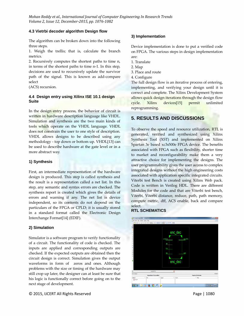
select. RTL SCHEMATICS
Page 6
Mohan Reddy et al., International Journal of Computer Engineering In Research Trends Volume 2, Issue 12, December-2015, pp. 1076-1082
© 2015, IJCERT All Rights Reserved Page | 1081
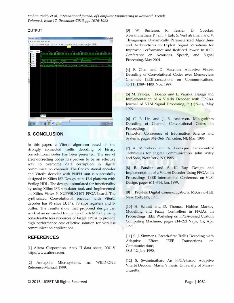
OUTPUT
6. CONCLUSION In this paper, a Viterbi algorithm based on the
strongly connected trellis decoding of binary
convolutional codes has been presented. The use of
error-correcting codes has proven to be an effective
way to overcome data corruption in digital
communication channels. The Convolutional encoder
and Viterbi decoder with PNPH unit is successfully
designed in Xilinx ISE Design suite 12.4 platform with
Verilog HDL. The design is simulated for functionality
by using Xilinx ISE simulator tool, and Implemented
on Xilinx Virtex-5, XUPV5LX110T FPGA board. The
synthesized Convolutional encoder with Viterbi
decoder has 96 slice LUT‟ s, 78 slice registers and 1-
buffer. The results show that proposed design can
work at an estimated frequency of 86.6 MHz by using
considerable less resources of target FPGA to provide
high performance cost effective solution for wireless
communication applications.
REFERENCES [1] Altera Corporation. Apex II data sheet, 2001.V
http://www.altera.com.
[2] Annapolis Microsystems, Inc. WILD-ONE
Reference Manual, 1999.
[3] W. Burleson, R. Tessier, D. Goeckel,
S.Swaminathan, P. Jain, J. Euh, S. Venkatraman, and V.
Thyagarajan. Dynamically Parameterized Algorithms
and Architectures to Exploit Signal Variations for
Improved Performance and Reduced Power. In IEEE
Conference on Acoustics, Speech, and Signal
Processing, May 2001.
[4] F. Chan and D. Haccoun. Adaptive Viterbi
Decoding of Convolutional Codes over Memoryless
Channels IEEETransactions on Communications,
45(11):1389– 1400, Nov. 1997.
[5] M. Kivioja, J. Isoaho, and L. Vanska. Design and
Implementation of a Viterbi Decoder with FPGAs.
Journal of VLSI Signal Processing, 21(1):5–14, May
1999.
[6] C. F. Lin and J. B. Anderson. M-algorithm
Decoding of Channel Convolutional Codes. In
Proceedings,
Princeton Conference of Information Science and
Systems, pages 362–366, Princeton, NJ, Mar. 1986.
[7] A. Michelson and A. Levesque. Error-control
Techniques for Digital Communication. John Wiley
and Sons, New York, NY,1985.
[8] B. Pandita and S. K. Roy. Design and
Implementation of a Viterbi Decoder Using FPGAs. In
Proceedings, IEEE International Conference on VLSI
Design, pages 611–614, Jan. 1999.
[9] J. Proakis. Digital Communications. McGraw-Hill,
New York, NY, 1995.
[10] H. Schmit and D. Thomas. Hidden Markov
Modelling and Fuzzy Controllers in FPGAs. In
Proceedings, IEEE Workshop on FPGA-based Custom
Computing Machines, pages 214–221,Napa, Ca, Apr.
1995.
[11] S. J. Simmons. Breath-first Trellis Decoding with
Adaptive Effort. IEEE Transactions on
Communications,
38:3–12, Jan. 1990.
[12] S. Swaminathan. An FPGA-based Adaptive
Viterbi Decoder. Master’s thesis, University of Massa-
chusetts,
Page 7
Mohan Reddy et al., International Journal of Computer Engineering In Research Trends Volume 2, Issue 12, December-2015, pp. 1076-1082
© 2015, IJCERT All Rights Reserved Page | 1082
Amherst, Department of Electrical and Computer
Engineering, 2001.
[13] R. Tessier and W. Burleson. Reconfigurable
Computing and Digital Signal Processing: A Survey.
Journal of VLSI Signal Processing, 28(1):7–27, May
2001.
[14] Texas Instruments, Inc. TMS320C6201 DSP Data
Sheet, 2001.
[15] Xilinx Corporation. Virtex II data sheet, 2001.
http://www.xilinx.com.