69
FPGA IMPLEMENTATION OF MULTI-CHANNEL CDMA DECODER A Bachelor’s thesis Project Rasmus Theodorsen København 2010
FPGA IMPLEMENTATION OF MULTI-CHANNEL CDMA DECODER A Bachelor’s thesis Project
Rasmus Theodorsen
København 2010

Technical University of Denmark Informatics and Mathematical Modelling Building 321, DK-2800 Kongens Lyngby, Denmark Phone +45 45253351, Fax +45 45882673 [email protected] www.imm.dtu.dk
Abstract
This report was made at the institute of Informatics & Mathematical Modelling at the Technical University of Denmark in partial fulfillment of the requirements for acquiring a Bachelor in engineering.
The report describes CDMA communication between several ground transmitters and a receiver in space. It covers CDMA communication in general and the issues of Doppler shifts between the transmitter and the receiver. A design is suggested for a parallel multichannel CDMA decoder that handles Doppler shifts and it has been implemented on an FPGA.

Acknowledgements
I would like to thank my two thesis advisers Hans Henrik Løvengreen and Edward Alexandru Todirica for their help and support during this project. I would also like to thank Teis Johansen whose insight on the subject has been a great help, and Isabella Bendixen who has supported me throughout the project and has helped editing this report.
Table of Contents
1 Introduction .................................................................................... 1
1.1 Introduction ............................................................................. 1
1.2 Problem statement .................................................................. 2
1.3 Previous work .......................................................................... 3
1.4 Specifications ........................................................................... 3
1.5 References ................................................................................ 4
2 Theory of CDMA communication .................................................. 5
2.1 Overview .................................................................................. 5
2.2 Transmission ........................................................................... 5
2.3 Decoding the signal ................................................................. 7
2.4 References .............................................................................. 11
3 Analysis ........................................................................................ 12
3.1 Overview ................................................................................ 12
3.2 Synchronization ..................................................................... 12
3.3 Acquisition ............................................................................. 12
3.4 Tracking ................................................................................. 14
3.5 Integrating acquisition and tracking .................................... 17
3.6 Frequency scheme ................................................................. 18
3.7 References .............................................................................. 20
4 Design ........................................................................................... 21
4.1 Overview ................................................................................ 21
4.2 Previous work ........................................................................ 21
4.3 Top level design ..................................................................... 22
4.4 Channel design ...................................................................... 24
4.5 Acquisition ............................................................................. 27
4.6 Tracking ................................................................................. 29
4.7 References .............................................................................. 32
5 Implementation ............................................................................ 33
5.1 Overview ................................................................................ 33

5.2 Hardware ............................................................................... 33
5.3 Entity diagram ...................................................................... 33
5.4 Channel.................................................................................. 34
5.5 Acquisition ............................................................................. 40
5.6 Tracking ................................................................................. 42
5.7 Size of implementation .......................................................... 45
6 Test environment ......................................................................... 47
6.1 Overview ................................................................................ 47
6.2 Simulator ............................................................................... 47
6.3 Input ...................................................................................... 48
6.4 Output .................................................................................... 49
6.5 References .............................................................................. 51
7 Test results ................................................................................... 52
7.1 Overview ................................................................................ 52
7.2 Multiple channels .................................................................. 52
7.3 Acquisition ............................................................................. 53
7.4 Tracking ................................................................................. 54
8 Future work .................................................................................. 59
9 Conclusion .................................................................................... 60
10 Bibliography ................................................................................. 61
11 Appendix ....................................................................................... 62
The source code for the VHDL implementation is appended on a CD.

1.1 Introduction 1
1 Introduction
1.1 Introduction This project is part of the DTUsat-II [1
The question is how the young cuckoo finds its way to Africa without any peers to guide it and without ever having been there before. Does it navigate intuitively or does it follow some predetermined generic route? That is the question that is attempted answered with this mission by tracking the bird from when it hatches until it arrives in Africa.
] mission in which students from the Technical University of Denmark (DTU) are responsible of designing and building a satellite for scientific research. The objective of the DTUsat-II mission is to track the migration of cuckoo birds. The cuckoo bird is a brood parasite, where the female lays an egg in the nest of a different bird species and leaves it there to hatch. After the offspring has hatched it is fed by the host until the young cuckoo is old enough to leave. Finally it will migrate south all alone spending the winter in Africa.
In order to track the cuckoo birds, these are equipped with a small solar driven transmitter. It consists of a GPS receiver which locates the position of the birds, and a radio transmitter which sends the location of the bird to the satellite.
Figure 1: Cube satellite [2] The satellite that is used to receive the signal is a cube satellite [3]. A cube satellite is a cubic 10cm3 satellite weighing at most 1kg (Figure 1). The limited size and weight of the satellite greatly constrains the amount of hardware that can be installed and it severely restricts the tolerated power dissipation of the satellite. The receiver in the satellite is in the DTUsat-II project referred to as the primary payload (PPL). The PPL processes the data from the bird transmitters and outputs the raw data, which is then processed and packed by a computer onboard the satellite. After decoding

Introduction 2
and packing the data it is sent back to a ground station for data analysis. The data flow is illustrated on Figure 2.
Figure 2: Abstract data flow
The PPL (Figure 3) consists of a radio receiver (which will not be covered in this report), an analog to digital (A/D) converter and a Code Division Multiple Access (CDMA) decoder used to decode the signals from the cuckoo bird transmitters. The CDMA decoder is the primary focus in this report.
Figure 3: PPL main blocks
1.2 Problem statement The bird transmitters all transmit on the same frequency so in order for the satellite to differentiate the signals from each other a system must be put into place. The CDMA technology enables the satellite to receive data from multiple birds that all transmit data simultaneously and on the same carrier wave frequency. This is achieved by coding each bird transmitter with a specific unique code. The CDMA decoder has a receiver for each of the unique codes and each of the receivers is referred to as a channel. Each channel can only pick up a signal transmitted with that code and channels holding a different code will see the signal as white noise. When a channel has acquired a signal it is therefore evident which bird the data comes from.
Besides allowing several channels to share the same carrier wave frequency, CDMA also displays fine properties when facing interference, since the signal is spread out over a much larger frequency range than the original data signal, hence limiting the effect of narrowband interference.
On board computer
Radiotransmitter
GPS receiver Radio transmitter
PPL
Radioreceiver
Dataanalysis
Ground station
Satellite
Bird transmitter
Data flow
Radioreceiver A/D converter
PPL
CDMA decoder
1.3 Previous work 3
Each channel must replicate the incoming carrier wave and the underlying unique code precisely in order to decode the signal. Since the receiver is orbiting in space there is bound to be a Doppler shift between the transmitted signal and the signal perceived by the receiver. Acquiring the signal is thus a matter of determining the Doppler shift in order to be able to replicate the incoming carrier wave and the unique code so that they match the incoming signal in both frequency and phase. The Doppler shift changes over time as the satellite moves so in order to keep track of the signal each channel must continuously adjust its frequencies.
The ability to transmit several signals on the same carrier wave frequency and the tolerance to noise is the reason why CDMA is used by the GPS system, and the reason why it is well-suitable for the DTUsat-II mission. The objective of this project is to implement the complete working multichannel CDMA decoder for use onboard the satellite. This involves integrating existing components into a multichannel parallel system, as well as designing new components to take care of acquiring the signal and tracking the Doppler shift of the signal continuously.
1.3 Previous work A project [4] has already taken place in which some of the design and implementation elements of the CDMA decoder were carried out.
It was decided that the CDMA decoder should be implemented on a Field Programmable Gate Array (FPGA) and the relevant frequencies for the carrier wave and the underlying modulated data as well as the A/D converter’s sampling rate were determined. Furthermore a complete design suggestion for a CDMA decoder was given and implementation of a single receiver channel was provided in the VHDL language.
1.4 Specifications Below are listed specifications which the implementation of the CDMA decoder must comply with.
• The implementation must be designed for an FPGA. • Based on the previous project a frequency scheme was suggested
which should be used. The frequencies are described in depth in chapter 3.
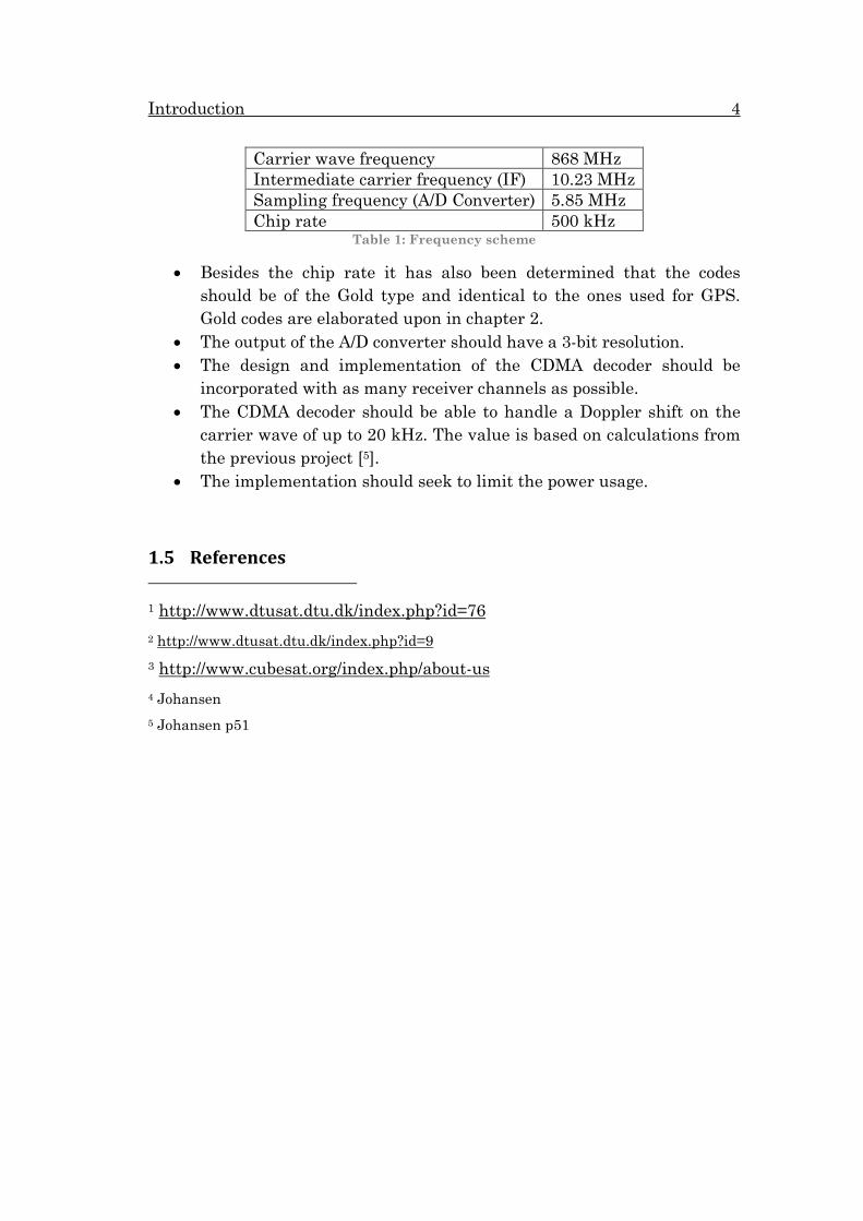
Introduction 4
Carrier wave frequency 868 MHz Intermediate carrier frequency (IF) 10.23 MHz Sampling frequency (A/D Converter) 5.85 MHz Chip rate 500 kHz
Table 1: Frequency scheme
• Besides the chip rate it has also been determined that the codes should be of the Gold type and identical to the ones used for GPS. Gold codes are elaborated upon in chapter 2.
• The output of the A/D converter should have a 3-bit resolution. • The design and implementation of the CDMA decoder should be
incorporated with as many receiver channels as possible. • The CDMA decoder should be able to handle a Doppler shift on the
carrier wave of up to 20 kHz. The value is based on calculations from the previous project [5].
• The implementation should seek to limit the power usage.
1.5 References 1 http://www.dtusat.dtu.dk/index.php?id=76 2 http://www.dtusat.dtu.dk/index.php?id=9 3 http://www.cubesat.org/index.php/about-us 4 Johansen 5 Johansen p51
2.1 Overview 5
2 Theory of CDMA communication
2.1 Overview This chapter goes through the theory of CDMA communication. It demonstrates how the digital signal is encoded and how it is modulated with the analog carrier wave. Furthermore it describes how the modulated carrier wave is decoded in order to output the original data. Finally it shows how the Gold sequences are created and what properties they reside.
2.2 Transmission CDMA communication is based on the use of Direct Sequence Spread Spectrum (DSSS) [6] signals on a shared sinusoid carrier wave, where each transmitter sends a uniquely encoded DSSS signal. DSSS signals are based on a modulation method such as Binary Phase Shift Keying (BPSK) [7], which uses the phase of the carrier wave to transmit a digital signal.
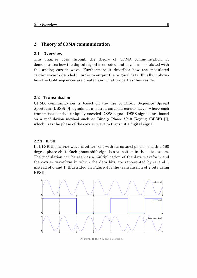
2.2.1 BPSK In BPSK the carrier wave is either sent with its natural phase or with a 180 degree phase shift. Each phase shift signals a transition in the data stream. The modulation can be seen as a multiplication of the data waveform and the carrier waveform in which the data bits are represented by -1 and 1 instead of 0 and 1. Illustrated on Figure 4 is the transmission of 7 bits using BPSK.
Figure 4: BPSK modulation
Theory of CDMA communication 6
Since the receiver of the signal has no way of knowing the natural phase of the transmitter it is unable to distinguish the phase shifted carrier from the natural, it is only able to determine the phase shifts as they come. Because of this there is a risk that the receiver will flip the entire data signal by perceiving the natural phase as the phase shifted phase and vice versa.
To overcome this issue the data signal typically has some overhead in which a sequence of bits known to the receiver is sent prior to the actual data stream. When the receiver receives the sequence it can tell if it is inverted and can flip the data signal entirely.
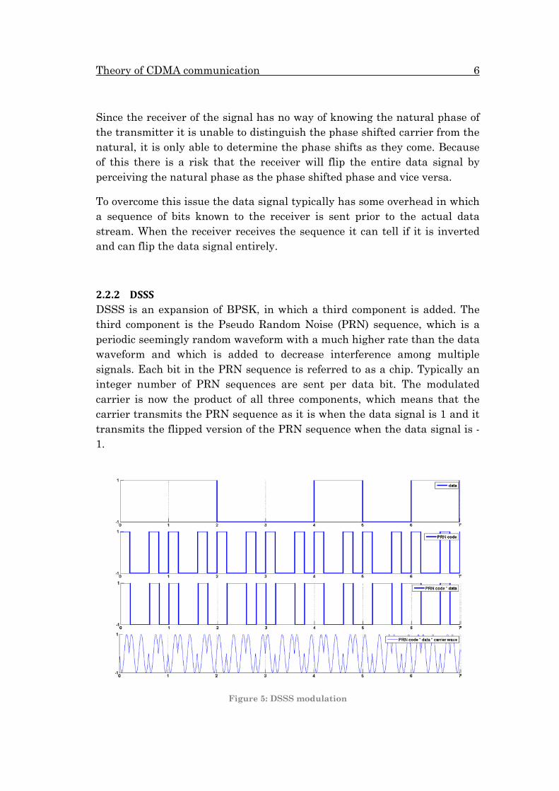
2.2.2 DSSS DSSS is an expansion of BPSK, in which a third component is added. The third component is the Pseudo Random Noise (PRN) sequence, which is a periodic seemingly random waveform with a much higher rate than the data waveform and which is added to decrease interference among multiple signals. Each bit in the PRN sequence is referred to as a chip. Typically an integer number of PRN sequences are sent per data bit. The modulated carrier is now the product of all three components, which means that the carrier transmits the PRN sequence as it is when the data signal is 1 and it transmits the flipped version of the PRN sequence when the data signal is -1.
Figure 5: DSSS modulation

2.3 Decoding the signal 7
In Figure 5 a data stream of 7 bits is sent and is multiplied with a PRN sequence of five chips. In this case the PRN sequence is run only once for each data bit. As illustrated the PRN sequence is sent in its normal order when the data bit is 1 and is flipped when the data bit is -1.
2.3 Decoding the signal To decode a single DSSS signal the first part is mixing the signal with a locally replicated sinusoid of the exact same phase and frequency as the carrier wave. That exposes the underlying PRN sequence as illustrated on Figure 6. In this case a chip has the length of one carrier wave period and a data bit has the length of five chips, or one PRN sequence. As illustrated on the bottom figure the waveform oscillates around ½ when the chip is 1 and -½ when it is -1.
Figure 6: Incoming signal mixed with local replica carrier wave with same frequency and phase
Still the signal is encoded with the PRN sequence so to expose the real data the signal is multiplied with the locally replicated PRN sequence of the same frequency and phase. The result of the multiplication is illustrated on Figure 7
Figure 7: Decoded signal

Theory of CDMA communication 8
Now in order to get the data bit value out, the signal is integrated over one full PRN sequence corresponding to the duration of one data bit. If the result of the integration is negative -1 is transmitted and if the integration result is positive +1 is transmitted. The magnitude of the integration is the correlation value. The correlation value is a measure of how well the PRN sequence replica and the carrier wave replica are aligned with the incoming signal. On Figure 7 they are perfectly aligned since the signal only changes after a data bit change.
The result of the integration is a 0Hz baseband signal. For the waveform in Figure 7 the equivalent baseband signal is illustrated below.
Figure 8: Decoded baseband data
The last step of decoding the original data is determining the mapping of the data bits. Either [-1, 1] [0, 1] or [-1, 1] [1, 0]. As mentioned before, this is done by transmitting a specific sequence of bits known to the receiver. If it is received upside down, the receiver can switch the mapping. In this case the original data (Figure 5) was the inverted of Figure 8. This means that the mapping should be [-1, 1] [1, 0] which is the opposite of the mapping used to transmit the data.
The raw data of the signal is now exposed and the decoding of the signal is complete.
2.3.1 Gold sequences When several DSSS signals with different PRN sequences share the same carrier frequency it is referred to as CDMA. In order to minimize interference among the signals, it is favorable to choose the PRN sequences in such a way that the correlation between two different sequences is very low while autocorrelation of a sequence is maximized for two perfectly aligned sequences and minimized for sequences that differ in phase. This makes it easier for the receiver to generate a perfectly aligned replica of the incoming sequence, which is required for decoding of the signal.
2.3 Decoding the signal 9
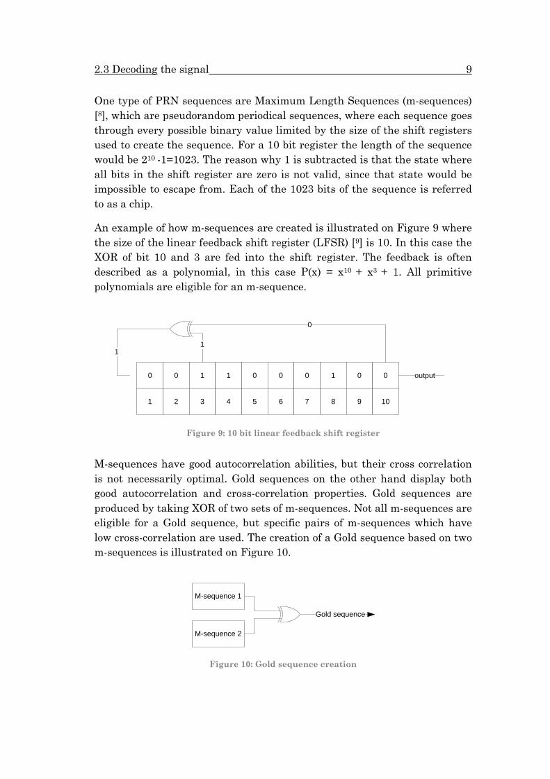
One type of PRN sequences are Maximum Length Sequences (m-sequences) [8], which are pseudorandom periodical sequences, where each sequence goes through every possible binary value limited by the size of the shift registers used to create the sequence. For a 10 bit register the length of the sequence would be 210 -1=1023. The reason why 1 is subtracted is that the state where all bits in the shift register are zero is not valid, since that state would be impossible to escape from. Each of the 1023 bits of the sequence is referred to as a chip.
An example of how m-sequences are created is illustrated on Figure 9 where the size of the linear feedback shift register (LFSR) [9] is 10. In this case the XOR of bit 10 and 3 are fed into the shift register. The feedback is often described as a polynomial, in this case P(x) = x10 + x3 + 1. All primitive polynomials are eligible for an m-sequence.
Figure 9: 10 bit linear feedback shift register
M-sequences have good autocorrelation abilities, but their cross correlation is not necessarily optimal. Gold sequences on the other hand display both good autocorrelation and cross-correlation properties. Gold sequences are produced by taking XOR of two sets of m-sequences. Not all m-sequences are eligible for a Gold sequence, but specific pairs of m-sequences which have low cross-correlation are used. The creation of a Gold sequence based on two m-sequences is illustrated on Figure 10.
Figure 10: Gold sequence creation
0 0 1 1 0 0 0 1 0 0
1 2 3 4 5 6 7 8 9 10
1
0
1
output
M-sequence 1
M-sequence 2
Gold sequence

Theory of CDMA communication 10
A pair of m-sequences that is eligible for a Gold code is called a preferred pair. For the architecture of GPS, 32 preferred pairs with the best correlation properties were selected for space usage. These are the Gold sequences that have been chosen for this project as well and will make it possible to equip up to 32 birds with transmitters.
Illustrated on Figure 11 are the auto- and cross-correlation abilities of some of these sequences. The top waveform shows the cross-correlation of two different Gold sequences, and it is clear that no matter the offset, the correlation values are very close to zero. The middle waveform shows auto-correlation of a Gold sequence. For all other offsets than around zero, the correlation values are low, but just around zero i.e. perfectly aligned is a peak. The bottom waveform gives a closer look at the peak, which shows that it only spans one chip on each side of zero, and that it is already halved at half a chip offset.
Figure 11: Gold sequence correlation properties
These are exactly the properties which are needed for the CDMA decoder. They make it easy to determine if two sequences are aligned and they cause a minimum of interference to each other.

2.4 References 11
2.4 References 6 Kaplan p114 7 Kaplan p113 8 http://en.wikipedia.org/wiki/Maximum_length_sequence 9 http://en.wikipedia.org/wiki/Linear_feedback_shift_register
Analysis 12
3 Analysis
3.1 Overview This chapter covers the prerequisites for the design of the CDMA decoder. It expands on the subsystems of the CDMA decoder and their functionalities and elaborates on the frequencies of the system.
3.2 Synchronization There are a number of requirements that have to be fulfilled before the decoding process can begin. The incoming carrier wave has to have the same frequency and phase as the locally replicated carrier wave and the transmitted Gold code has to be perfectly aligned with the locally replicated Gold code.
Under stationary circumstances the frequency of the transmitted carrier and underlying Gold code would not change, but since the receiver is going to be placed in orbit in space there is going to be a significant Doppler shift between the frequency of the transmitted signal and the signal perceived by the receiver. In order to start decoding the signal that Doppler shift has to be determined. This process is referred to as acquisition.
Additionally the Doppler shift is going to change dynamically over time as the satellite moves and hence the receiver will have to be able to adapt to a change in the frequency of the incoming signal and keep the replicated signals in sync with the frequencies of the incoming signal. Maintaining the frequencies of the replicated signals is referred to as tracking.
The preliminary determination of the Doppler shift and the continuous tracking of the Doppler shift lead to a division of the Doppler shift compensation into two parts, acquisition and tracking.
3.3 Acquisition Acquisition is the process of locating the frequency and phase of the incoming signal. It consists of two parts, finding the correct frequency and phase of the carrier wave and finding the correct phase of the Gold sequence. The Gold sequence will experience little Doppler shift, since its rate is relatively low (500 kHz) compared to the carrier frequency (868 MHz)
3.3 Acquisition 13
and the frequency of the Gold code can therefore be ignored during acquisition.
There are a number of ways to perform acquisition. Some methods use Fourier transformations which makes it possible to do acquisition in fewer steps. Parallel Frequency Space Search Acquisition [10] uses one Fourier transformation and eliminates the carrier frequency as an unknown, leaving only the Gold sequence phase to be determined. Parallel Code Phase Search Acquisition [11] uses two Fourier transformations and one inverse Fourier transformation and eliminates the Gold sequence phase as unknowns leaving only the carrier frequency to be determined. These designs can decrease the execution time of acquisition, but they both complicate the implementation and require relatively heavy computations.
A simpler but more time consuming method is called Serial Search Acquisition [12] and is basically a trial and error approach. Inside the channel every possible combination of carrier wave frequency and Gold code phase within the anticipated frequency range is tried until a signal appears.
The maximum Doppler shift of the carrier wave should be around ±20kHz. The Gold sequence consists of 1023 chips, and the phase has to be located within half a chip’s accuracy.
That leaves a lot possible combinations of Gold code phase and carrier wave frequency. The exact number of possible combinations depends upon the implementation. The carrier frequencies have to be adjusted by some step size. For a carrier frequency step size of 500Hz [13] that would leave 80 different frequencies to be tried. For the Gold code, the phase can be moved by two chips at a time resulting in 512 different possibilities. In total that leaves 40960 different possibilities.
For each possibility one full Gold sequence is typically run with those settings and the correlation value is compared with a threshold in order to determine if the frequency and phase of the replicated signals are correct. For a 1023 chips Gold sequence running each chip at 500 kHz the channel spends approximately 2ms integrating over the full Gold sequence. To iterate all possible frequencies and phases would then take 40960∙2ms ≈ 84s.
Acquisition could in fact take up almost twice that time, since the transmitted signal could reach the receiver at a time where the correct frequency had just been tried by acquisition. It is estimated that the receiver and the transmitter will have a window of approximately 10 minutes to

Analysis 14
establish a connection and transmit data [14], so it is quite important that acquisition is precise and does not give false positives nor neglects to pick up on a valid signal.
3.4 Tracking Tracking is the process of constantly keeping the locally replicated Gold sequence and carrier wave synchronized with the incoming signal after it has been picked up by acquisition. As the Doppler shift changes the tracking is to accommodate to the changes and keep the signal in a lock at all time. To accomplish this, tracking makes use of loop filters.
Loop filters are meant to filter noise and respond to dynamically changing conditions. They receive an error signal on the input known as the discriminator and produce an output which in this case can be used to control the frequency of the carrier wave replica or the frequency of the replica Gold sequence. The goal of the loop filter is to minimize the error output so that the frequencies need not be adjusted, but are perfectly locked in.
Figure 12: Tracking overview
Figure 12 shows how the signal decoder (Channel) outputs correlation values, which are used to calculate the discriminator which then is used as the input of the loop filter. The loop filter then calculates a frequency offset and adjusts the decoder.
3.4.1 Carrier tracking For the carrier wave tracking a Phase Locked Loop (PLL) [15] is often used. It makes use of two locally replicated carriers 90 degrees apart, to create the in-phase component (I) and the quadrature component (Q). Correlating the incoming signal with both replicas makes it possible to calculate the phase difference (φ) between the local in-phase replica and the incoming signal. The phase difference is then used as the discriminator of the loop filter. By determining if the local replica either lags the incoming signal or is ahead of
DecoderIncoming signal DiscriminatorI
QLoop filter
Frequency adjustment

3.4 Tracking 15
it, the loop filter adjusts the frequency of the replica accordingly increasing the frequency if the replica lags behind and decreasing the frequency if the replica is ahead.
Discriminator Output Comment Q*I Sin(2*φ) Near optimal at low SNR Q*sign(I) Sin(φ) Near optimal at high SNR Q/I Tan(φ) Suboptimal at low and high SNR ARCTAN(Q/I) φ Optimal
Table 2: PLL discriminators [16]
Table 2 shows several different discriminator possibilities for the PLL. The first two are the ones requiring the least computational burden, but they have the disadvantage of being dependant on the amplitude of the Q and I values and are only optimal for specific signal to noise ratios (SNR). The last two are not dependant on amplitude and work for both high and low SNR, but require dividers, which results in a heavier computational burden. The discriminators all have that in common that they are Costas discriminators, which means that they are insensitive to 180 degree phase shifts, which is crucial for DSSS communication.
3.4.2 Code tracking To track the Gold code replica a Delay Locked Loop (DLL) [17] is well suitable. It works by having three locally replicated Gold sequences each half a chip apart in phase hence the first one (IE) is one chip apart from the last (IL). When the replica is perfectly synced the middle (IP) will have maximum correlation and IE and IL will have half the value of IP in accordance with the waveform depicted on Figure 13.
Figure 13: The three phases of the DLL
The discriminator produces an error output based on the difference between IE and IL and sends it to the loop filter which adjusts the frequency accordingly increasing the frequency if IE increases and vice versa.
Discriminator Comment

Analysis 16
½ [(IE-IL)IP + (QE-QL)QP] Near optimal at ±0.5 chip offset Amplitude dependent
¼ [(IE-IL) / IP + (QE-QL) / QP] Near optimal at ±0.5 chip offset Amplitude independent
Table 3: DLL discriminators [18]
The discriminators in Table 3 use both the quadrature and the in-phase components to estimate an exact error output making use of a total of six correlators. The top discriminator is the easiest to implement, but has the disadvantage of being amplitude dependent while the other is normalized, but requires two divisions making the computational burden heavier. Other discriminators are also available, but they do not use all six correlators which is preferable for a stable output.
3.4.3 Loop filters Both the carrier- and code tracking can share the same loop filter, where the only difference is the discriminator. Loop filters exist in various complexities known as orders. From a first order loop filter which is no more than a multiplication of the discriminator to more advanced second and third order loop filters containing integrators and several adjustable variables. A first order loop can only be used to track the phase of a carrier, while a second order loop can track a frequency offset i.e. Doppler shift. A third order loop filter is insensitive to acceleration stress and can thus be used to dynamically track the Doppler shift as it changes over time.

3.5 Integrating acquisition and tracking 17
Figure 14: first, second and third order loop filters [19]
Illustrated on Figure 14 are three loop filters of different order. The triangles are multipliers and the Z-1 boxes are integrators. T is the time between the loop filter is updated and is thus also the period between each integration step. 𝜔0 is the natural radian frequency and a and b are filter constants.
The parameters of the loop filters are adjustable, but guidelines for the parameters do apply. The natural frequency is based on the noise bandwidth (BN) selected by the designer. Suggested parameters [20] for a third order loop filter are shown below based on a noise bandwidth of 18Hz.
𝜔0 =𝐵𝑛
0.7845 = 22.94455 𝑟𝑎𝑑/𝑠
𝑎3 = 1,1,𝑏3 = 2.4
3.5 Integrating acquisition and tracking Acquisition has a preset frequency stepping size, which is typically quite coarse. That means that it might surpass the actual frequency of the carrier and end at a frequency that picks up a signal, but can be several hundreds of Hertz from the actual frequency.
∑
ω0
ω02 T
a2ω0
Z-1
∑ ∑1/2
∑ω03 T
a3ω02
Z-1
∑ ∑1/2 ∑T
Z-1
∑ ∑1/2
b3ω0
Analysis 18
When acquisition ends and tracking takes over it is expected to be able to adjust the frequency from where acquisition ended to the actual frequency. The main strength of the PLL tracking is on maintaining a signal that is already locked in so it might not be able to successfully adjust a signal that is hundreds of Hertz off and thus there might be a grey area between where acquisition ends and tracking takes over where none of the two is able to track the signal.
Decreasing the acquisition stepping size will not resolve this issue since acquisition will end as soon as a signal is found. Having a smaller stepping size will cause acquisition to end at the furthest frequency away from the actual frequency offset where the signal is still picked up. Instead ideally there should be only one frequency step where the signal is picked up.
The frequency range between where acquisition stops and tracking takes over must therefore be handled by a third system, a finer acquisition that with a smaller step size tries frequencies in the area of where acquisition stops and finally picks the frequency with the best correlation.
3.6 Frequency scheme A particular frequency scheme which should be used for the implementation was chosen in the previous project. The frequencies are shown in Table 4.
Carrier Frequency 868 MHz Intermediate carrier frequency (IF) 10.23 MHz Sampling frequency (A/D converter) 5.85 MHz Gold code chip rate 511.5 kHz
Table 4: Frequency scheme
The carrier frequency is the frequency of the carrier wave. The 868 MHz frequency was chosen because it is within the Industrial, Scientific and Medical (ISM) radio band. This frequency band is open for use without a license and results in reasonable antenna length. The carrier frequency will experience Doppler shifts in the order of +-20 kHz.
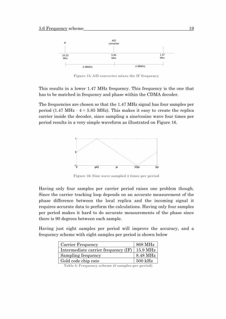
The IF frequency is the frequency after the carrier has been mixed with an 878.23 MHz frequency. The IF is a more manageable frequency for the A/D converter. The A/D converter’s sampling frequency will act as a second mixer mirroring the IF frequency as illustrated on Figure 15.
3.6 Frequency scheme 19
Figure 15: A/D converter mixes the IF frequency
This results in a lower 1.47 MHz frequency. This frequency is the one that has to be matched in frequency and phase within the CDMA decoder.
The frequencies are chosen so that the 1.47 MHz signal has four samples per period (1.47 MHz ∙ 4 ≈ 5.85 MHz). This makes it easy to create the replica carrier inside the decoder, since sampling a sine/cosine wave four times per period results in a very simple waveform as illustrated on Figure 16.
Figure 16: Sine wave sampled 4 times per period
Having only four samples per carrier period raises one problem though. Since the carrier tracking loop depends on an accurate measurement of the phase difference between the local replica and the incoming signal it requires accurate data to perform the calculations. Having only four samples per period makes it hard to do accurate measurements of the phase since there is 90 degrees between each sample.
Having just eight samples per period will improve the accuracy, and a frequency scheme with eight samples per period is shown below
Carrier Frequency 868 MHz Intermediate carrier frequency (IF) 15.9 MHz Sampling frequency 8.48 MHz Gold code chip rate 500 kHz
Table 5: Frequency scheme (8 samples per period)
5.85 Mhz
10.23 Mhz
IFA/D
converter
1.47 Mhz
4.38MHz 4.38MHz
Analysis 20
This scheme requires higher frequencies, but it will make the tracking loop work better.
3.7 References 10 Borre p78 11 Borre p81 12 Borre p76 13 Borre p75 14 Johansen p50 15 Kaplan p165 16 Kaplan p168 17 Kaplan p173 18 Kaplan p174 19 Kaplan p181 20 Kaplan p183

4.1 Overview 21
4 Design
4.1 Overview This chapter begins with an introduction to the work that has been done in the previous project. The components introduced in the previous chapter are elaborated upon and actual block level designs of the overall design of the CDMA decoder as well as the individual sub components are given.
4.2 Previous work Since this project is a continuation of a previous project, some of the components for the CDMA decoder where already built and examples of designs given. Illustrated on Figure 17 is the design which had already been implemented. It is basically a full decoder channel except that the clock dividers where not adjustable, but fixed at a preset frequency. Consequently there is no feature to adjust the frequency and phase of the Gold sequence and the sine/cosine as is needed for acquisition of the signal and for tracking the Doppler shift.
Figure 17: Already implemented design (Channel)
Still missing from the design is the entire tracking and acquisition parts and the integration of these with the existing implementation. Furthermore the existing implementation is not prepared to be tested on an actual FPGA since the A/D simulator relies on file access from the computer, which is not possible on an FPGA. To test the implementation on an FPGA either a signal has to be stored on the board or a communication link to an external storage has to be established.
Signal file
SIN
COS
Clock divider
Clock divider
Gold Sequence
I
EarlyPrompt
Late
Integrate & Dump
Integrate & Dump
Integrate & Dump
Integrate & Dump
Integrate & Dump
Integrate & Dump
Q
EarlyPrompt
Late
IE
IP
IL
QL
QP
QE
A/D simulator Controller
Data
Address
WriteEnable
ReadEnable

Design 22
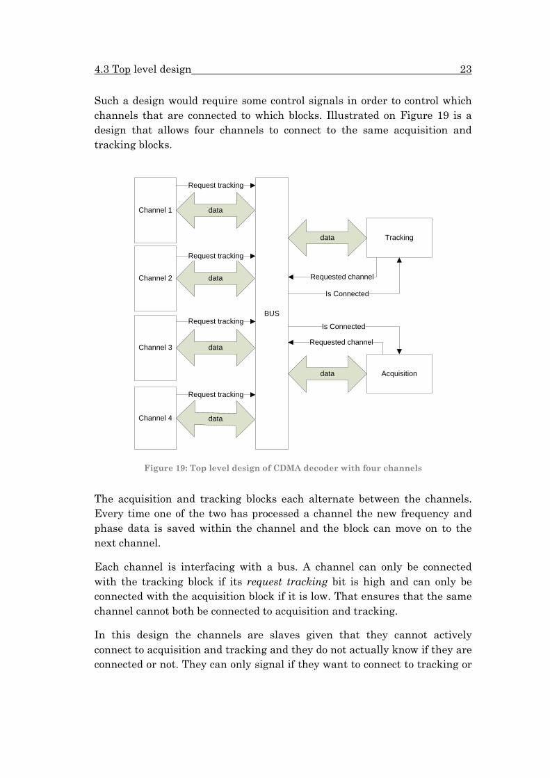
4.3 Top level design The CDMA decoder consists of the actual decoder, the tracking block and the acquisition block. Illustrated on Figure 18 is the connectivity of the three. The channel must be connected to either tracking or acquisition, it cannot connect to both.
Figure 18: CDMA decoder channel during tracking
When designing for multiple channels the design from above could simply be copied for each channel so that there is one acquisition and one tracking block for each channel. That would however not be the most efficient way to design the multi-channel CDMA decoder.
The reason for that is that the channel only updates its correlation values when it has integrated over a full Gold sequence, and that tracking or acquisition only needs to do any work whenever those correlation values are updated. For a chip rate of 500 kHz the correlation values take about 2ms to update. The correlation values are thus updated at a manageable 500Hz rate. For a system clock frequency of 50MHz on the FPGA that leaves 100,000 clock cycles to perform the acquisition or tracking calculations.
The calculations of acquisition and tracking do however not take more than about 10-30 clock cycles so that leaves enough time to calculate the output thousands of times. Furthermore a channel can only connect to either acquisition or tracking so one of the blocks will be completely unused by the channel.
A more efficient way to implement the design would be to let multiple channels share the same acquisition and tracking blocks. The 32 channels could easily share the same acquisition and tracking blocks since they still would have plenty of time to do their calculations. Sharing the resources would decrease the overall power usage of the design quite a bit, since the calculation of the discriminator and the calculations inside the loop filter take up a lot of resources. Limiting the power usage is also one of the design goals and is therefore an important parameter.
Channel
Tracking
Correlation values
Frequency/phase adjustments
sample
Acquisition
4.3 Top level design 23
Such a design would require some control signals in order to control which channels that are connected to which blocks. Illustrated on Figure 19 is a design that allows four channels to connect to the same acquisition and tracking blocks.
Figure 19: Top level design of CDMA decoder with four channels
The acquisition and tracking blocks each alternate between the channels. Every time one of the two has processed a channel the new frequency and phase data is saved within the channel and the block can move on to the next channel.
Each channel is interfacing with a bus. A channel can only be connected with the tracking block if its request tracking bit is high and can only be connected with the acquisition block if it is low. That ensures that the same channel cannot both be connected to acquisition and tracking.
In this design the channels are slaves given that they cannot actively connect to acquisition and tracking and they do not actually know if they are connected or not. They can only signal if they want to connect to tracking or
Channel 1
Channel 2
Tracking
Acquisition
BUS
Requested channel
Is Connected
Requested channel
Is Connected
Channel 3
Channel 4
data
data
data
data
data
data
Request tracking
Request tracking
Request tracking
Request tracking

Design 24
acquisition, and that choice is in fact made by tracking and acquisition since they set the signal.
Tracking and acquisition on the other hand can actively choose which channel they wish to connect to. When tracking sets the requested channel signal and if the selected channel has set its request tracking signal high the tracking block is connected to the channel and it is signaled from the bus by setting the is connected bit high.
The design on Figure 19 can easily be scaled to contain even more channels it is only a matter of adding ports to the bus and extending the requested channel signal to incorporate all channels. The 32 channels can therefore easily be implemented using this design.
4.4 Channel design
4.4.1 Decoder The design of the decoder is illustrated on Figure 20. The design only shows the decoding part of the channel and not the integration with the rest of the design.
Figure 20: Decoder
The sample is the 3-bit value that is the output of the A/D converter. It is updated at the A/D converter’s sample rate. First step in the decoding process is multiplying the sample with a sine and a cosine. The cosine is the one used for the in-phase component containing the actual data and the sine is used for the quadrature component solely used for tracking the signal. Both the in-phase and quatrature components are multiplied with three Gold sequences which each differ in phase by half a chip. This results in
sample
SIN
COS
Gold sequence Frequency
divider
Carrier Frequency
divider
Gold Sequence Generator
I
EarlyPrompt
Late
Integrate & Dump
Integrate & Dump
Integrate & Dump
Integrate & Dump
Integrate & Dump
Integrate & Dump
Q
EarlyPrompt
Late
IE
IP
IL
QL
QP
QE

4.4 Channel design 25
three in-phase signals and three quadrature signals. Each of them is integrated for the duration of a full Gold sequence. When the Gold sequence is over the correlation values are dumped into holding registers inside the channel and the integrators are reset. These registers hold the values until the integrators are done with the next Gold sequence after which their values are overwritten with the new correlation values.
4.4.1.1 Gold sequence generator The Gold sequence generator inside the decoder is responsible of producing the specific periodic Gold sequence chosen for that channel. It is to output three versions of the Gold sequence each half a chip apart from each other. This is accomplished by having a two bit shift register running at twice the frequency of the Gold sequence.
Figure 21: Gold sequence delays
The Gold sequence itself can be created using shift registers with feedback as illustrated on Figure 22
Figure 22: Gold sequence generator [21]
Gold sequence
Early Prompt Late
1 2 3 4 5 6 7 8 9 10
1 2 3 4 5 6 7 8 9 10
sequence

Design 26
Each specific Gold sequence differs in taps, which are the two outputs that are XOR’ed from the bottom register (dotted line on the figure). 32 different taps form the 32 different Gold sequences.
The disadvantage of this design is that it is relatively troublesome to enable phase delay of the sequence in both directions which is required to align the generated Gold code with the one of the incoming signal. Instead, since the sequence is periodic it can be stored in the memory of the FPGA and accessed by an address pointer as will be described in the implementation chapter.
4.4.1.2 Frequency divider Both the Gold sequence clock and the carrier clock are created using the frequency divider. The non-integer adjustable frequency divider is a component capable of outputting a clock at an adjustable frequency. It consists of an adder and a register and the amount added to the register controls the output frequency (fout).
𝑓𝑜𝑢𝑡 =𝑏𝑎𝑠𝑒 ∙ 𝑓𝑠𝑦𝑠
2𝑤𝑖𝑑𝑡ℎ
Base is the amount added to the register each clock cycle, fsys is the system clock frequency and width is the amount of bits in the register. The more bits in the register the more precise is the outputted clock. The minimum frequency step size of the frequency divider (the resolution) is given by 𝑓𝑠𝑦𝑠/2𝑤𝑖𝑑𝑡ℎ. To adjust the frequency in accordance with a Doppler shift an offset is added to the base as shown on Figure 23.
Figure 23: Non-integer frequency divider
Figure 23 illustrates the frequency divider, where the phase accumulator is the part consisting of the register and the adder.
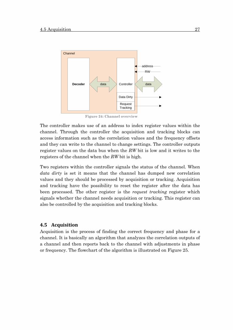
4.4.2 Controller Illustrated on Figure 24 is the controller which is associated with each channel. It drives the communication between the channel and the tracking and acquisition blocks.
∑base
offset
Phase accumulator Fbase + Foffset
4.5 Acquisition 27
Figure 24: Channel overview
The controller makes use of an address to index register values within the channel. Through the controller the acquisition and tracking blocks can access information such as the correlation values and the frequency offsets and they can write to the channel to change settings. The controller outputs register values on the data bus when the RW bit is low and it writes to the registers of the channel when the RW bit is high.
Two registers within the controller signals the status of the channel. When data dirty is set it means that the channel has dumped new correlation values and they should be processed by acquisition or tracking. Acquisition and tracking have the possibility to reset the register after the data has been processed. The other register is the request tracking register which signals whether the channel needs acquisition or tracking. This register can also be controlled by the acquisition and tracking blocks.
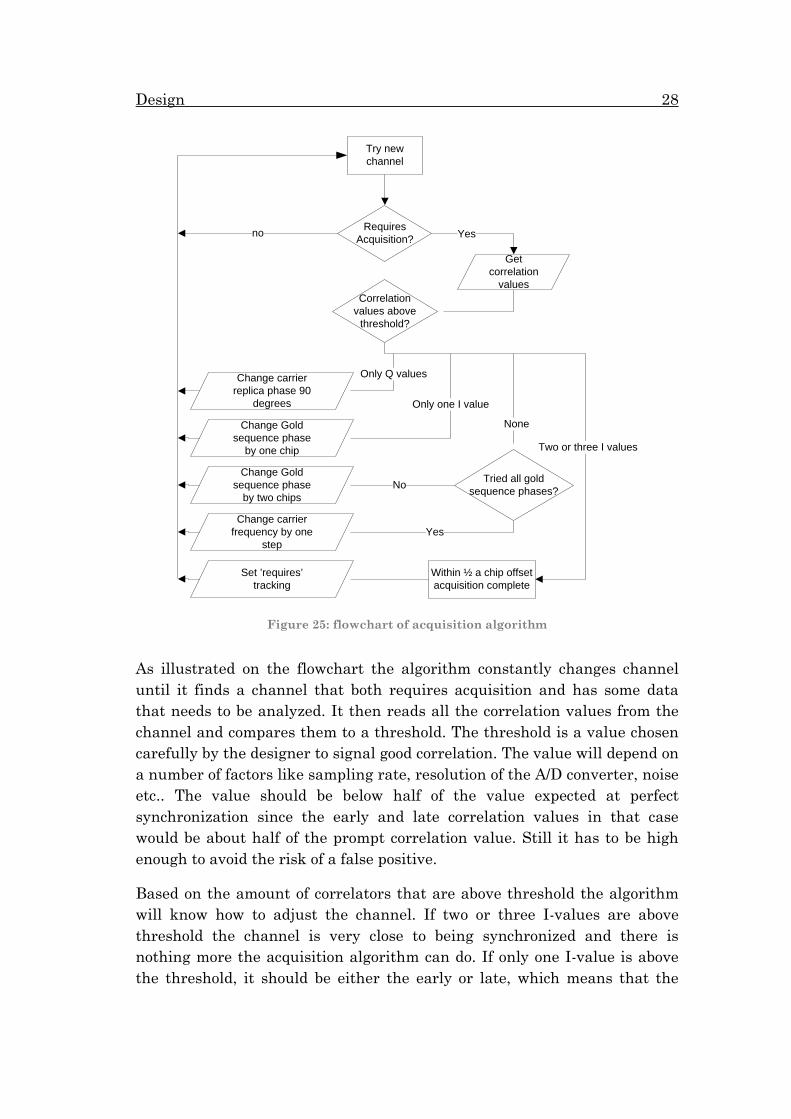
4.5 Acquisition Acquisition is the process of finding the correct frequency and phase for a channel. It is basically an algorithm that analyzes the correlation outputs of a channel and then reports back to the channel with adjustments in phase or frequency. The flowchart of the algorithm is illustrated on Figure 25.
Controllerdata
Channel
Decoder data
address
RW
Request Tracking
Data Dirty
Design 28
Figure 25: flowchart of acquisition algorithm
As illustrated on the flowchart the algorithm constantly changes channel until it finds a channel that both requires acquisition and has some data that needs to be analyzed. It then reads all the correlation values from the channel and compares them to a threshold. The threshold is a value chosen carefully by the designer to signal good correlation. The value will depend on a number of factors like sampling rate, resolution of the A/D converter, noise etc.. The value should be below half of the value expected at perfect synchronization since the early and late correlation values in that case would be about half of the prompt correlation value. Still it has to be high enough to avoid the risk of a false positive.
Based on the amount of correlators that are above threshold the algorithm will know how to adjust the channel. If two or three I-values are above threshold the channel is very close to being synchronized and there is nothing more the acquisition algorithm can do. If only one I-value is above the threshold, it should be either the early or late, which means that the
Try new channel
Yes
Q values only
Only one I value
Within ½ a chip offset acquisition complete
Two or three I values
None
No
Yes
Requires Acquisition?
Get correlation
valuesCorrelation
values above threshold?
Tried all gold sequence phases?
Change carrier replica phase 90
degrees
no
Only Q values
Change Gold sequence phase
by one chip
Change Gold sequence phase
by two chips
Change carrier frequency by one
step
Set ’requires’ tracking
4.6 Tracking 29
channel is off by only one chip and acquisition will tell the channel to change the phase one chip in the appropriate direction. If only Q-values are above threshold the carrier replica must be about 90 degrees out of phase and thus acquisition will make the channel change the replica carrier phase by 90 degrees. If neither I-values nor Q-values are above threshold, the channel will be more than one chip off and acquisition will make the channel change phase by two chips. If all phases of the Gold sequence are unsuccessful it will change the carrier frequency offset of the channel by one step. The step size is the amount of Hertz the carrier frequency is changed each time the acquisition block changes the frequency. This parameter should be carefully selected to be small enough that the signal is not skipped entirely, but large enough to limit the amount of frequencies the acquisition block must try and thereby limiting the acquisition time. After each change the flow starts over cycling through channels until a new request is found.
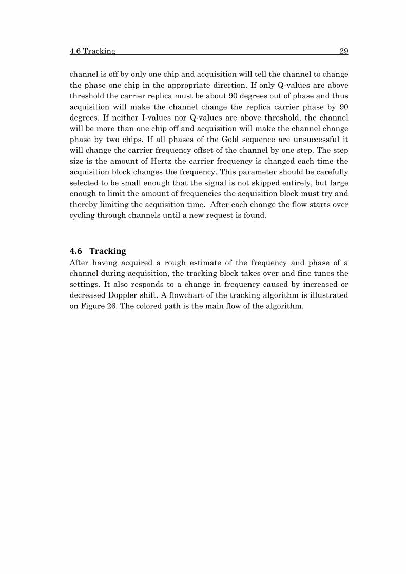
4.6 Tracking After having acquired a rough estimate of the frequency and phase of a channel during acquisition, the tracking block takes over and fine tunes the settings. It also responds to a change in frequency caused by increased or decreased Doppler shift. A flowchart of the tracking algorithm is illustrated on Figure 26. The colored path is the main flow of the algorithm.
Design 30
Figure 26: Flowchart of tracking algorithm
It starts similar to the acquisition algorithm by cycling through channels until it finds one that requires tracking and has unprocessed data. When a channel has been found it reads the correlation values. When all correlation values are loaded it checks to see if the signal has been lost and will have to be acquired again. If not it calculates the Gold code discriminator and starts the loop filter. It waits for the loop filter to finish and then adjusts the Gold code frequency accordingly. After having updated the Gold code frequency it changes the discriminator of the loop filter to the carrier tracking discriminator and restarts the filter. When the filter is done it adjusts the carrier frequency, and starts over waiting for a new channel that requires tracking.
Try New channel
Requires tracking? Yes
Get correlation
values
Start Loop FilterWith Code
DiscriminatorLoop filter done?
Adjust carrier
frequency
Start loop filter with carrier
discriminator
Loop filter done?
No
Adjust Gold code
frequency
Correlator values below threshold?
Yes
No
YesClear
’request tracking’
No
No
Yes
4.6 Tracking 31
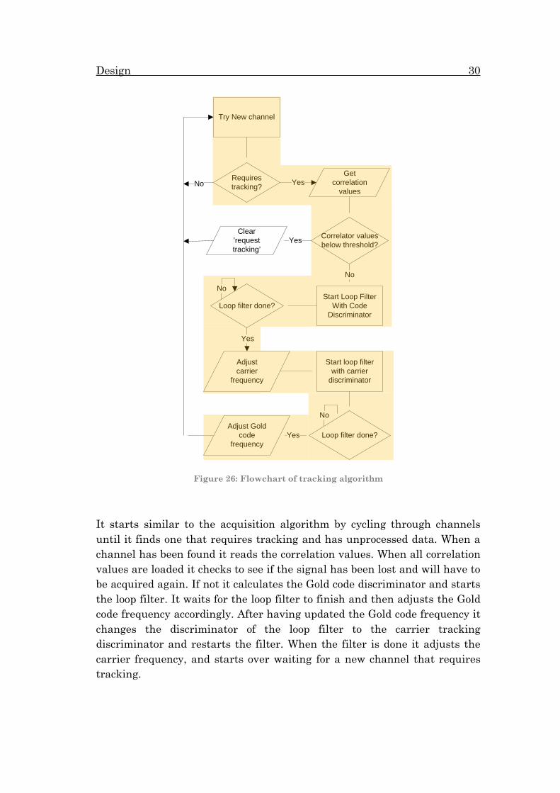
4.6.1 Loop filter The loop filter used in the tracking algorithm is the 2nd order loop filter illustrated on Figure 27.
Figure 27: 2nd order loop filter [22]
The loop filter illustrated above has two storage elements. One saves the previous value of the discriminator and one accumulates the output of the loop filter. The advantage of this design is that both of the storage elements can be placed outside the actual loop filter.
The previous discriminator can be fed as an input to the loop filter together with the current discriminator. The accumulator can actually be integrated into the channel block. The loop filter can simply output the value that is to be added to the accumulator and that value can then be added to the existing frequency offset of the channel, a value that is already present within the channel. The design is illustrated below.
Figure 28: Loop filter design
The parameters used for the loop filter are based upon recommended values [23] and are shown below.
𝜔 = 37.736
𝑎2 = 1.414
𝑇 = 0.002
+
+
+
+
-
+
+
Z-1
ω02 T ∑
a2ω0∑
+ ∑
Discriminator Z-1∑
+
-
+
+ω02 T ∑
a2ω0∑
Previous discriminator
Discriminator
output
Design 32
To ease the implementation discriminators without dividers are chosen for both carrier and Gold sequence tracking. For carrier tracking the discriminator 𝑄 ∗ 𝑠𝑖𝑔𝑛(𝐼) is best for high signal to noise ratio, which is the case when testing the design in the simulator. The discriminator 𝑄 ∗ 𝐼 is optimal at low signal to noise ratios and should be used under those circumstances, as could be expected for the real signals received in space.
For Gold sequence tracking the discriminator 0.5(𝑄𝐸 − 𝑄𝐿)𝑄𝑃 + 0.5(𝐼𝐸 − 𝐼𝐿) is used, which is near optimal at all signal to noise ratios.
4.7 References 21 Johansen p69 22 Borre MATLAB code (DVD) 23 Kaplan p180
5.1 Overview 33
5 Implementation
5.1 Overview This chapter covers the choice of hardware for the implementation and gives details on the implementation of each component of the CDMA decoder.
5.2 Hardware The CDMA decoder is highly parallel since all channels are decoded simultaneously. For the maximum of 32 channels it would be too demanding for a processor to keep up, which is why custom hardware is required. For this project an FPGA has been selected since it is highly customizable and much cheaper than a custom built solution such as an ASIC. The whole implementation is carried out in the VHDL language.
The tracking and acquisition could be implemented on a processor since those blocks do not need to work in parallel and are not required to work as fast as the decoder channels. However since tracking and acquisition are relatively simple algorithms to implement on an FPGA, they will take up less space than to dedicate an entire processor, and consequently it was natural to carry everything out on the FPGA.
All components have been implemented using Xilinx Project Navigator and have been tested to run on a Digilent Virtex-2 Pro FPGA board. The system clock used is 50MHz.
5.3 Entity diagram The diagram on Figure 29 shows all entities present in the implementation of the CDMA decoder.

Implementation 34
Figure 29: All entities of the CDMA decoder
5.4 Channel The channel entity includes the whole decoder as well as the controller that handles communication.
The base frequency of the generated Gold code and the carrier wave is preset by the designer using generic values. Generic values are constants that are set once and for all before the implementation is downloaded to the FPGA board. Also chosen by generics are the Gold code tabs. They are chosen from a value between 0 and 31 each representing a unique Gold code. Finally a pointer to a text file containing the Gold code sequences is required. When initiating a channel the generics make it easy to choose a specific Gold code as well as setting the frequencies.
The channel entity is a shell which consists of several sub-entities which interact to perform the behavior of a channel. Each sub-entity is described in the following.
5.4.1 Generator The channel entity routes the requested Gold code number through to the generator entity which is responsible of outputting the Gold code in the three time delayed versions early, prompt and late. The generator receives a clock which runs twice the actual chip rate and thus it needs a clock divider
Controller
Gold sequence clock divider
Carrier wave clock divider
Sine mixer
Cosine mixer
2-bit shift register
Gold code generatorQ prompt
mixerQ late mixer
Q late mixer
I late mixer
Q prompt mixer
Q late mixer
Q prompt mixer
I prompt mixer
Q early mixer
I early mixer
Correlator
Generator Mixer
Channel
Loop Filter
Tracking
Acquisition
Bus
5.4 Channel 35
that halves the frequency so that both the slow and the fast clock are present within the entity. The fast clock is used to clock the 2-bit shift register which holds the early, prompt and late versions of the code, and the slow clock is used to clock the Gold sequence inside the Gold code generator.
The entire Gold sequence is contained in a memory block inside the Gold code generator where each of the 1023 chips can be accessed by setting the address accordingly. Each time the entity is clocked by the slow clock the address is incremented and the next chip in the sequence is outputted. When the address reaches 1022 the next address will be zero and a correlation dump signal will be issued signaling that the correlators should dump their integrations values into a register and start over.
The acquisition entity will however sometimes change the routine by signaling a phase change. The phase can be changed by -1, 1 or 2 chips. When that happens the offset will be added to the address pointer. This will typically not cause any problems, but the addition might result in a value above the expected maximum of 1022. A subroutine therefore checks the result of the addition and sets the address pointer to a valid value. After an offset the code generator must signal the controller that it has completed the phase change and that the offset input should be reset.
Note that the offset is a 2-bit signal which normally for a two’s complements number would give the range -2 to 1. In this implementation the values are inverted since the value -2 could cause a negative address value, which is undesirable. For the acquisition block it makes no difference except that when a partial signal is present it should transmit -1 instead of 1 or vice versa. For no signal it does not matter which way the Gold code changes phase as long as it is done persistently.
5.4.2 Mixer The mixer entity receives a 3-bit signal from the A/D Converter and multiplies it with a sine and a cosine respectively. The sine and cosine each consist of eight phases per period and each phase is represented as a 4-bit sign & magnitude value. The value is determined from a map where each of the eight phases is associated with an integer between 0 and 7 as shown on Table 6. A counter increments the phase value causing the sine and cosine output to change.
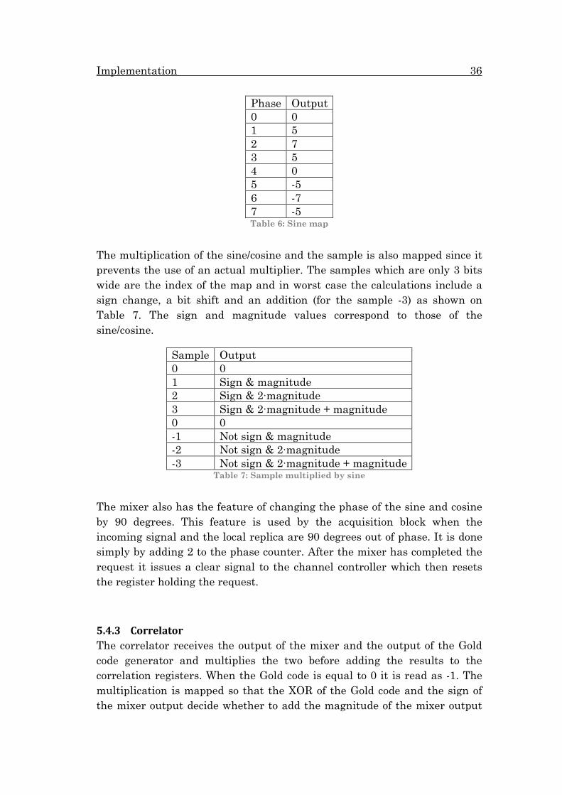
Implementation 36
Phase Output 0 0 1 5 2 7 3 5 4 0 5 -5 6 -7 7 -5 Table 6: Sine map
The multiplication of the sine/cosine and the sample is also mapped since it prevents the use of an actual multiplier. The samples which are only 3 bits wide are the index of the map and in worst case the calculations include a sign change, a bit shift and an addition (for the sample -3) as shown on Table 7. The sign and magnitude values correspond to those of the sine/cosine.
Sample Output 0 0 1 Sign & magnitude 2 Sign & 2∙magnitude 3 Sign & 2∙magnitude + magnitude 0 0 -1 Not sign & magnitude -2 Not sign & 2∙magnitude -3 Not sign & 2∙magnitude + magnitude
Table 7: Sample multiplied by sine
The mixer also has the feature of changing the phase of the sine and cosine by 90 degrees. This feature is used by the acquisition block when the incoming signal and the local replica are 90 degrees out of phase. It is done simply by adding 2 to the phase counter. After the mixer has completed the request it issues a clear signal to the channel controller which then resets the register holding the request.
5.4.3 Correlator The correlator receives the output of the mixer and the output of the Gold code generator and multiplies the two before adding the results to the correlation registers. When the Gold code is equal to 0 it is read as -1. The multiplication is mapped so that the XOR of the Gold code and the sign of the mixer output decide whether to add the magnitude of the mixer output
5.4 Channel 37
or to subtract it from the correlation register. If the XOR is 1 the two have the same sign, since 0 is negative and 1 is positive for the Gold sequence and opposite for the sign bit of the mixer, and thus the magnitude should be added to the register. If the XOR is 0 the two differ in sign and the magnitude should be subtracted.
When the Gold code generator issues the correlation dump signal the correlators save their values in the dump registers after which the correlator registers are reset. Since the correlator entity receives both the three, time delayed values of the Gold code and the two 90 degrees phase delayed carrier replicas a total of six correlator values are outputted.
5.4.4 Frequency divider The frequency dividers are implemented using a generic to choose the width of the accumulation register, but in this implementation the calculations are based on a 32-bit register.
Each channel has two frequency dividers, one for generation of the Gold sequence and one for generation of the carrier wave. The frequency outputted by the Gold sequence frequency divider is double the chip rate i.e. 2∙500kHz = 1MHz.
To generate this frequency the base should be:
232 ∙ 1MHz50MHz = 85,899,346
For the carrier wave frequency there are two options depending on the frequency scheme. For the option with the 8.48MHz sampling rate the base would be:
232 ∙ 8.48MHz50MHz = 728,426,453
For the option with the 5.85MHz sampling rate the frequency base should be:
232 ∙ 2 ∗ 5.85MHz50MHz = 1,005,022,347
For the 5.85MHz sampling rate the twice the frequency is made since the mixer has eight phases per period for the sine/cosine, but the incoming signal only has four. The mixer is therefore sampled at twice the 5.85MHz

Implementation 38
rate while the correlator is sampled at the original 5.85MHz rate by dividing the created frequency by two.
The clock frequencies inside the channel sample at eight times the frequency of the incoming signal in order to output eight sine/cosine values during one period of the incoming signal. To get a 20 kHz Doppler shift inside the channel the clock frequencies must change by eight times that value i.e. 160 kHz. For the frequency divider that corresponds to a value of 232∙0.16MHz
50MHz= 13,743,895. To store this signed value requires 25 bits. The offset
signal for the frequency divider must therefore be 25 bits wide.
5.4.5 Controller The controller is the bridge between the channel and the rest of the system. The controller consists of a 2∙16-bit data bus which enables it to output register values stored within the channel, such as the dumped correlation values, and to receive commands from the acquisition and tracking blocks. To select which data to send and receive an 8-bit address signal is used. Each register has an address and is accessed by setting the address signal accordingly. Finally the RW signal is used to determine if there should be read from the registers or written to the registers. When the signal is low the controller will read from the addressed register and make the data accessible on the dataR signal. When the RW signal is high it will store the content of the dataW signal in the addressed register.
The addressing and communication of the controller is illustrated on Figure 30.

5.4 Channel 39
Figure 30: Controller
The first six addresses are the dumped correlation results of the channel. They can only be read and are each 16 bits wide.
Address six and seven are used to select the frequency offsets of the Gold sequence clock. Address six holds the highest 16 bits and address seven holds the lowest 9.
Address eight and nine hold the equivalent frequency offsets for the carrier wave replica. The offsets can both be written and read. Address 10 adjusts the phase of the gold sequence. It is a two-bit signal since the phase can only be moved by up to two chips at a time. The phase offset is selected by setting the two least significant bits of the DataW signal. It is only possible to write to address 10 since the phase is not stored. The channel automatically resets the register when the Gold sequence has been successfully phase delayed.
Address 11 and 12 control the Request Tracking bit, which has a separate signal out to ease access for tracking and acquisition, since it is used quite often in order to decide whether to process a channel. The Request Tracking bit which is zero at default is a bit which signals if the channel requires acquisition or tracking. When the bit is low only acquisition can connect to
Controller
RW
DataW
Address
DataR
Request tracking
Data dirty
IP [16 bit] R
IE [16 bit] R
QE [16 bit] R
IL [16 bit] R
QL [16 bit] R
QP [16 bit] R
Gold code frequency offset low [9 bit] RW
Gold code frequency offset high [16 bit] RW
Carrier frequency offset low[9 bit] RW
Carrier frequency offset high[16 bit] RW
Clear request tracking[1 bit] W
Change Gold code phase
[2 bit] W
Clear data dirty[1 bit] W
Set request tracking[1 bit] W
Change carrier phase 90°[1 bit] W
0
2
4
6
8
10
12
14
RegisterAddr.
Implementation 40
the channel and when the bit is high only tracking can connect. After acquisition has located a signal it can set the bit high by writing to address 12 and likewise if tracking suddenly loses the signal, the tracking block can set the bit low by writing to address 11.
Address 13 is used to clear the Data Dirty bit. Data Dirty is set high by the channel each time new values are dumped into the correlation dump registers. Since this signal is used quite often by acquisition and tracking it also has its own output. Data Dirty signals the acquisition and tracking blocks that it is time to analyze the channel’s data and when that has been done acquisition or tracking should clear the bit by writing to this address.
For address 14 it is possible to change the phase of the carrier replica by 90 degrees by writing to this address. The register is reset automatically when the phase change is accomplished.
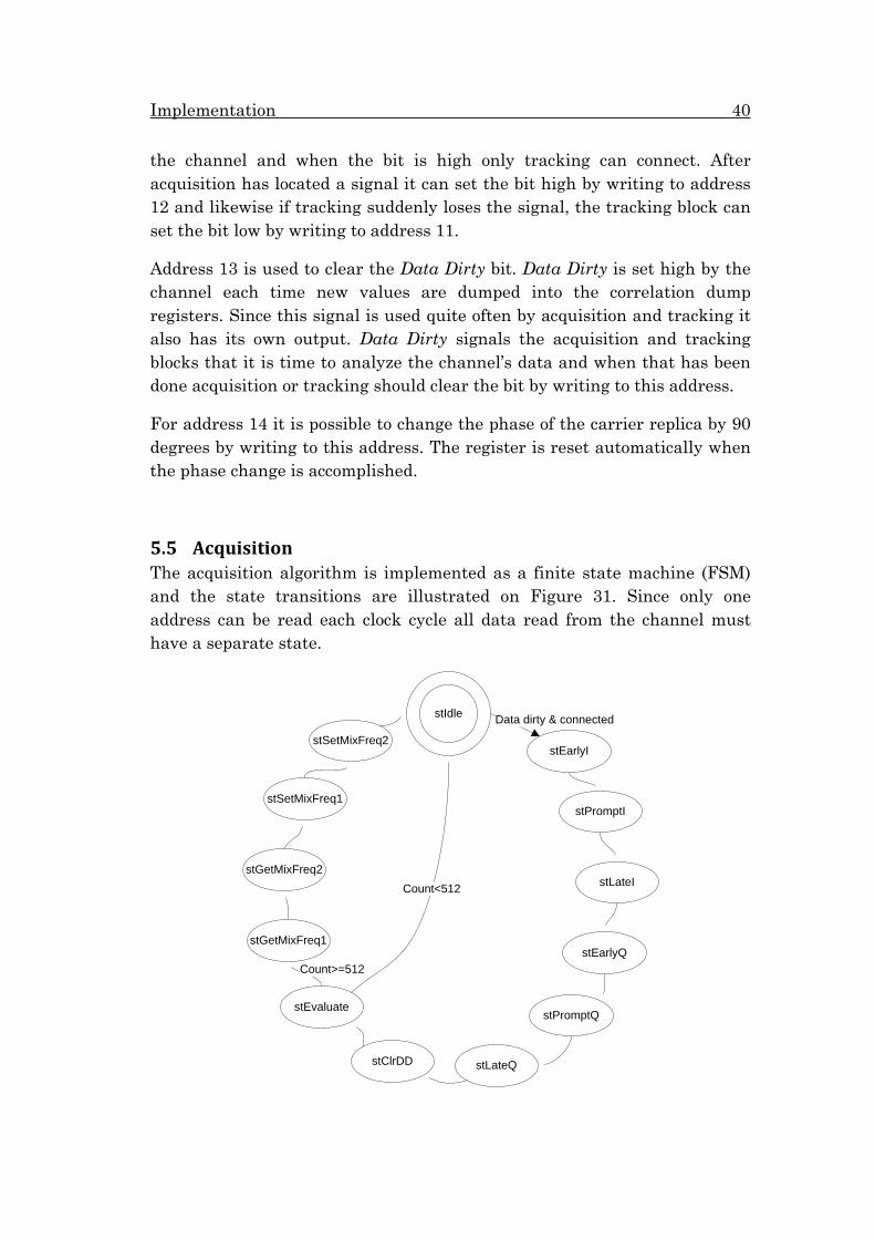
5.5 Acquisition The acquisition algorithm is implemented as a finite state machine (FSM) and the state transitions are illustrated on Figure 31. Since only one address can be read each clock cycle all data read from the channel must have a separate state.
stIdle
stEarlyI
stPromptI
stLateI
stEarlyQ
stPromptQ
stLateQstClrDD
stEvaluate
stGetMixFreq1
stGetMixFreq2
stSetMixFreq1
stSetMixFreq2
Data dirty & connected
Count>=512
Count<512
5.5 Acquisition 41
Figure 31: Acquisition FSM
The default state is stIdle. This state toggles through all channels continuously and is only exited if a channel has the request tracking bit low while also having the data dirty bit high. This means that a channel needs acquisition and has unprocessed data.
The next six states read the six correlation values from the channel. For each state it compares the read value with a threshold and if the value is above that threshold a success bit is set, if it is not the success bit is left low.
After having read the correlation values the data dirty bit is cleared in stClrDD. It is cleared since the data now is about to be processed and thus will not need processing until new values are present in the correlation registers.
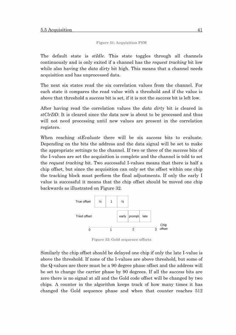
When reaching stEvaluate there will be six success bits to evaluate. Depending on the bits the address and the data signal will be set to make the appropriate settings to the channel. If two or three of the success bits of the I-values are set the acquisition is complete and the channel is told to set the request tracking bit. Two successful I-values means that there is half a chip offset, but since the acquisition can only set the offset within one chip the tracking block must perform the final adjustments. If only the early I value is successful it means that the chip offset should be moved one chip backwards as illustrated on Figure 32.
Figure 32: Gold sequence offsets
Similarly the chip offset should be delayed one chip if only the late I-value is above the threshold. If none of the I-values are above threshold, but some of the Q-values are there must be a 90 degree phase offset and the address will be set to change the carrier phase by 90 degrees. If all the success bits are zero there is no signal at all and the Gold code offset will be changed by two chips. A counter in the algorithm keeps track of how many times it has changed the Gold sequence phase and when that counter reaches 512
early prompt late
½ 1 ½
0 1 2 3Chip offset
True offset
Tried offset
Implementation 42
without a valid signal, the algorithm will have tried all possible phase delays and must try a new frequency.
The FSM will then go into stGetMixFreq1, where it will get the 16 most significant bits (MSB) of the existing mixer frequency offset from the channel. In stGetMixFreq2 it gets the least significant 9 bits (LSB).
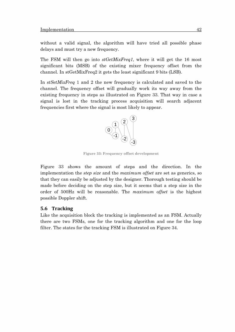
In stSetMixFreq 1 and 2 the new frequency is calculated and saved to the channel. The frequency offset will gradually work its way away from the existing frequency in steps as illustrated on Figure 33. That way in case a signal is lost in the tracking process acquisition will search adjacent frequencies first where the signal is most likely to appear.
Figure 33: Frequency offset development
Figure 33 shows the amount of steps and the direction. In the implementation the step size and the maximum offset are set as generics, so that they can easily be adjusted by the designer. Thorough testing should be made before deciding on the step size, but it seems that a step size in the order of 500Hz will be reasonable. The maximum offset is the highest possible Doppler shift.
5.6 Tracking Like the acquisition block the tracking is implemented as an FSM. Actually there are two FSMs, one for the tracking algorithm and one for the loop filter. The states for the tracking FSM is illustrated on Figure 34.
0-1
1
-2
2
-3
3

5.6 Tracking 43
Figure 34: Tracking FSM
The first states are almost identical to those of the acquisition block. StIdle is the default state which tries different channels until a request for tracking appears. The correlation values are fetched from the channel one at a time and finally the state changes to stCheckSignal. This state checks if all correlation values are below the threshold, and if they are the signal has been lost and the channel is told to clear the request tracking bit. If not the state changes to stCodeTrack1 where the 16 MSB of the Gold sequence frequency offset is fetched and the discriminator for the Gold code tracking is calculated and sent to the loop filter, which is signaled to begin. In stCodeTrack2 the 9 LSB of the offset are fetched and the state does not change until the loop filter is done calculating. When the loop filter is done the state changes to stAdjustCode 1 and 2. These states add the output of the loop filter to the existing frequency offset. The state then changes to stCarrierTrack 1 and 2 which fetch the carrier wave frequency offset, calculate the carrier replica discriminator and start the filter. When the
Valid signal
stIdle
stEarlyI
stEarlyQ
stLateQ
stLateI
stPromptI
stPromptQ
stCheck signal
stCodeTrack1
stAdjustCarrier1
stCodeTrack2
stAdjustCode1
stAdjustCode2
stAdjustCarrier2
stCarrierTrack1
stCarrierTrack2
stClrDD
No valid signal
Data dirty & connected
Implementation 44
filter is done the high and low bits of the output is added to the existing offset in stAdjustCarrier 1 and 2 and finally the FSM returns to its default state.
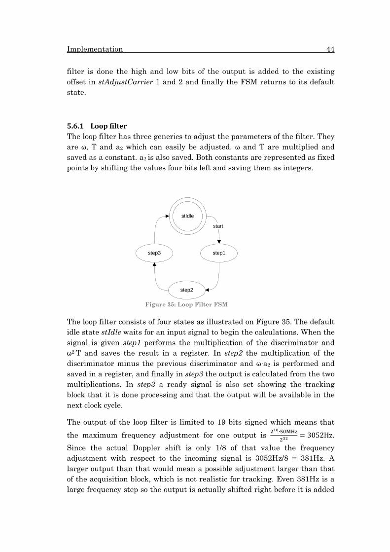
5.6.1 Loop filter The loop filter has three generics to adjust the parameters of the filter. They are ω, T and a2 which can easily be adjusted. ω and T are multiplied and saved as a constant. a2 is also saved. Both constants are represented as fixed points by shifting the values four bits left and saving them as integers.
Figure 35: Loop Filter FSM
The loop filter consists of four states as illustrated on Figure 35. The default idle state stIdle waits for an input signal to begin the calculations. When the signal is given step1 performs the multiplication of the discriminator and ω2∙T and saves the result in a register. In step2 the multiplication of the discriminator minus the previous discriminator and ω∙a2 is performed and saved in a register, and finally in step3 the output is calculated from the two multiplications. In step3 a ready signal is also set showing the tracking block that it is done processing and that the output will be available in the next clock cycle.
The output of the loop filter is limited to 19 bits signed which means that the maximum frequency adjustment for one output is 2
18∙50MHz232
= 3052Hz. Since the actual Doppler shift is only 1/8 of that value the frequency adjustment with respect to the incoming signal is 3052Hz/8 = 381Hz. A larger output than that would mean a possible adjustment larger than that of the acquisition block, which is not realistic for tracking. Even 381Hz is a large frequency step so the output is actually shifted right before it is added
stIdle
step1
step2
step3
start
5.7 Size of implementation 45
to the offset of the channel. The amount of bits the output is shifted right controls how large fluctuations in frequency the tracking block should perform.
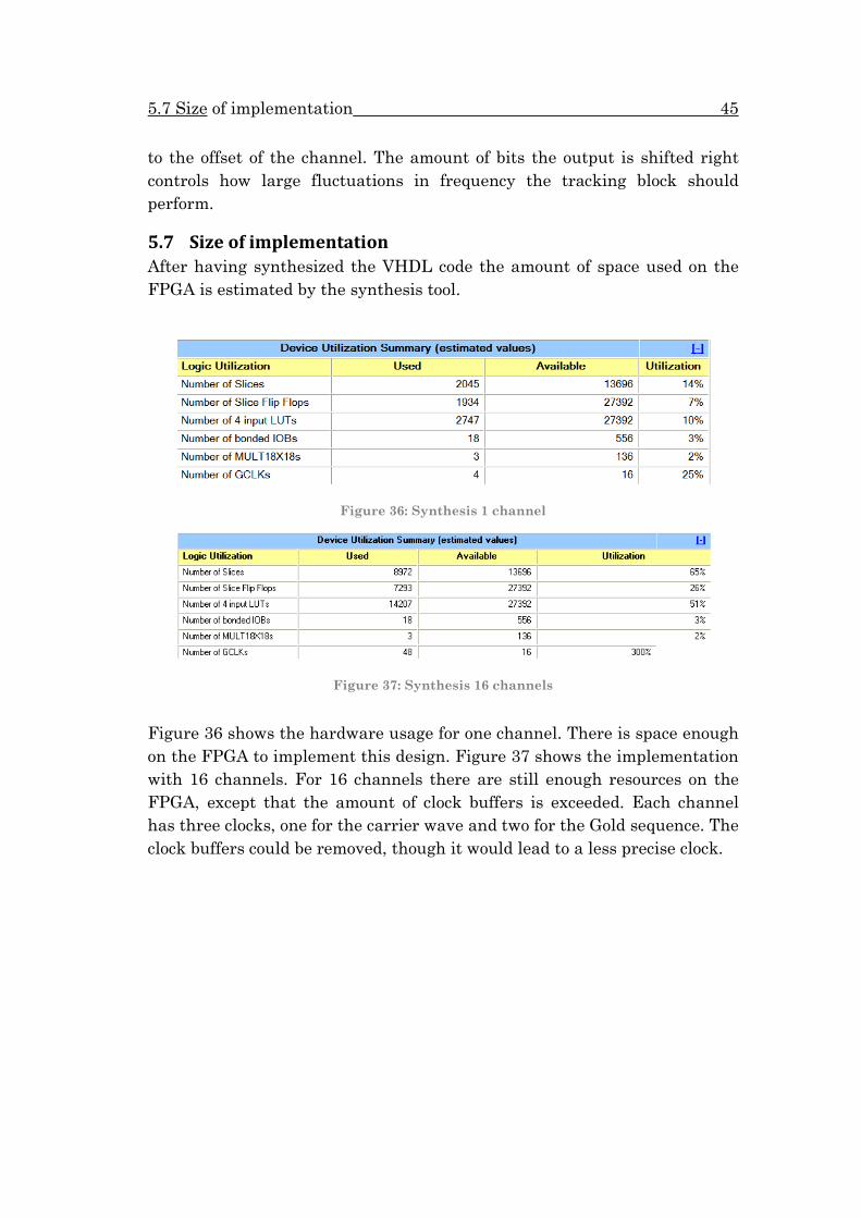
5.7 Size of implementation After having synthesized the VHDL code the amount of space used on the FPGA is estimated by the synthesis tool.
Figure 36: Synthesis 1 channel
Figure 37: Synthesis 16 channels
Figure 36 shows the hardware usage for one channel. There is space enough on the FPGA to implement this design. Figure 37 shows the implementation with 16 channels. For 16 channels there are still enough resources on the FPGA, except that the amount of clock buffers is exceeded. Each channel has three clocks, one for the carrier wave and two for the Gold sequence. The clock buffers could be removed, though it would lead to a less precise clock.

Implementation 46
Figure 38: Synthesis 32 channels
The Virtex-II board cannot contain all 32 channels since the utilized number of slices is more than the capacity of the FPGA. To use all 32 channels would require a slightly larger FPGA.
6.1 Overview 47
6 Test environment
6.1 Overview The test environment section covers the setup of the environment used to test the implementation on the FPGA. It describes the different possibilities for inputting a simulated signal to the FPGA and for getting data out of the FPGA.
6.2 Simulator In order to be able to test the design of the CDMA decoder a software simulator has been provided [24]. It is eligible of producing signals based on the Gold sequences and with any set of frequencies. It is also possible to mix noise into the signal and to mix several signals with different Gold sequences in order to simulate actual CDMA. It can simulate a fixed Doppler shift, but its only limitation is that it is unable to simulate a Doppler shift that changes over time, such as it would be the case in space. A mean to test this behavior is thus still missing. This simulator is the basis of all the tests run in simulation and on the FPGA.
The signal is created based on parameters from a configuration file. The most important parameters are given below.
Variable Description codeNo A value between 1 and 32 that
corresponds to the 32 different Gold codes.
F_0 The carrier wave frequency. F_osc The mixing frequency. F_s The sampling rate of the A/D converter. F_c The chip code rate of the Gold code.
Table 8: Simulator parameters
After the parameters have been set a data file has to be created using the generatedatafile tool from the simulator software. This tool creates the actual data to transmit. Originally the simulator was set to randomize the data, but in order to easily be able to check that the data is decoded correctly it is changed so that the output alternates between 0 and 1 continuously.
The next step is generating the signal file. The signal is created using the genSignal tool which makes a signal based on the data file and the
Test environment 48
configuration file. Finally it is possible to mix several generated signals using the mixSignals tool.
The outputted signal file is however not ready to be used with the implementation since it is outputted as 64-bit floating point values. The implemented design relies upon 3-bit sign & magnitude values so a conversion has to be made.
6.3 Input The signal generated by the simulator must be converted so that the FPGA can read it. Besides the signal file must be transferred to the FPGA and the FPGA must be able to read a new value from the file at the speed of the sampling rate. Two methods of converting and transferring the signal file to the FPGA are given below.
6.3.1 Memory One way of making the samples available for the FPGA is to store the samples in the block RAM of the FPGA. The board used has 2448 kilobit of block RAMs. Xilinx Project Navigator is able to read a textual representation of the bits to be stored in the memory. A text file containing each 3-bit sample is therefore required. To convert from the 64-bit floating point values of the signal file to the 3-bit text file a small VHDL file is made. It is based on a file from the previous project [25], but where the previous file outputted the 3 bits as a signal this file saves them as text in a file.
The only problem is that the amount of memory in the FPGA is only enough to store a very short length of signal. Each sample is 3 bits and with a sample rate of approximately 5.85MHz, the storage is only large enough to store a signal length lasting about 70 Gold sequences which is only a fraction of a second worth of samples.
To be able to test acquisition and tracking of the system a much longer signal is required. This is possible by looping the signal, so that it starts over after an integer number of Gold sequences. The advantage of this is an unlimited signal, but a disadvantage is that small timing glitches will appear when the signal loops bringing the signal slightly out of phase which is not good when testing tracking. The other disadvantage is only being able to test the system on a short segment of a signal.

6.4 Output 49
6.3.2 USB connection Another possibility is the use of a USB connection to transmit a signal in real-time to the FPGA. The advantage of this is that it is possible to test a longer signal and one avoids the glitches from looping. A disadvantage is that the FPGA will run out of samples when a file has been transmitted and thus there is a limit to the amount of time the FPGA has to operate.
To establish the USB connection a Digilent USB Module [26] is used. Digilent also supplies an API (Digilent Adept SDK) which can be used to transfer a file through the USB connection. The default method for doing so could however not be used since it sends the data in small packages where each package begins with an address. The FPGA needs a constant feed of samples so it would lose the signal every time a new package was sent. Instead the API is changed so that the package size becomes the size of the signal file. That way only one package is sent.
The USB module is set to send 8 bits at the time and it reads them directly from a binary file. The output of the simulator has to be converted from the 64-bit floating point values to the 3-bit sign & magnitude values packed inside a byte. The byte can thus contain two samples. A MATLAB script is made to handle this conversion.
Inside the FPGA the receiving part of the USB module is placed. This part must follow the protocol of the USB transfer. A VHDL file that implements this behavior is provided by Digilent [27]. The file is changed so that it would output a new sample every time a clock signal was clocked and would receive a new byte every other time the signal was clocked since each byte contains two samples.
6.4 Output In order to verify the results of the CDMA decoder some means of visually checking the status of the FPGA is required. In simulation on the computer this is easily done in a tool like ModelSim, but on the FPGA it is a bit more complicated. Two methods have been used and they are described below.
6.4.1 Serial The first is a serial RS-232 connection between the FPGA and a computer. The serial connection is relatively easy to implement since it only relies on one transmission line to transmit data. An UART component (Universal

Test environment 50
Asynchronous Receiver/Transmitter) can then be used to transmit an 8-bit signal. When transmitting 8-bit ASCII codes a program such as Hyperterminal can be used to receive and visualize the data as characters on a computer.
Figure 39: Serial communication
Illustrated on Figure 39 is the protocol of the serial communication. In this case the transmission of the data [1, 1, 0, 1, 0, 0, 1, 0]. Each transmission begins with a start-bit which is zero and ends with a stop bit which is one, when nothing is transmitted the line is just logical high. The bit rate is typically quite low for this kind of communication, in this implementation 19.2 kb/s including overhead corresponding to 1920 characters per second. Correlating over a full Gold sequence takes about 2ms, so it is possible to transmit up to three characters per correlation. An obvious choice is just transmitting the data bit of the channel as a character. The advantage of the serial connection is that data is outputted continuously with no need for storage within the FPGA, while the downside is a limited bandwidth.
The implementation of the serial connection is based on existing VHDL code [28]
6.4.2 ChipScope Another possibility is the use of ChipScope. ChipScope is a tool that is able to show waveforms of signals from the FPGA on a computer. It uses the internal block RAMs of the FPGA to store the signals and thus there is a limit to the amount of data which can be stored. But it is capable of storing many signals and the signals to store can easily be changed, which makes it a versatile tool for debugging and data analysis.
startidleidle bit0 bit1 bit2 bit3 bit4 bit5 bit6 bit7 stop idle

6.5 References 51
6.5 References 24 Poulsen 25 Johansen input.vhd 26 http://digilentinc.com/Products/Detail.cfm?NavPath=2,398,728&Prod=USB2 27 http://digilentinc.com/Data/Products/ADEPT/dpimref.vhd 28 Chu
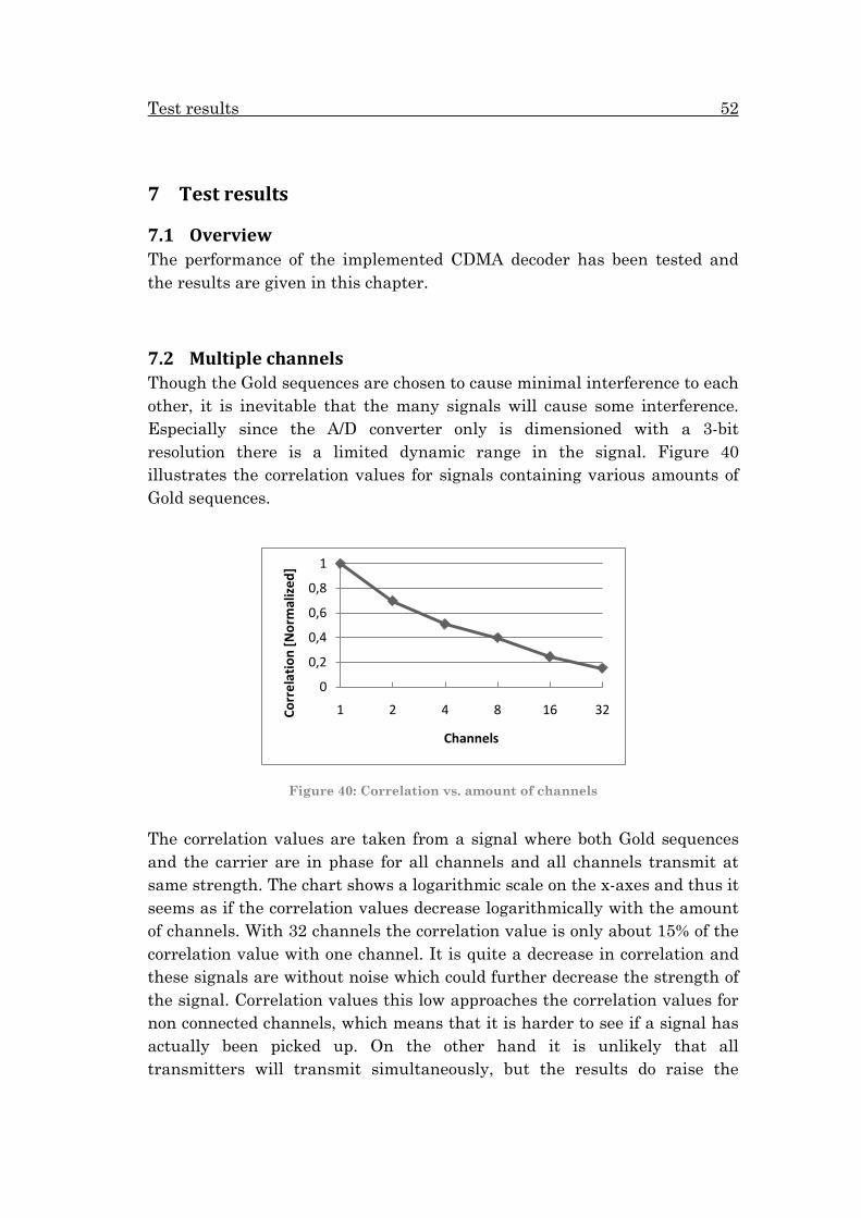
Test results 52
7 Test results
7.1 Overview The performance of the implemented CDMA decoder has been tested and the results are given in this chapter.
7.2 Multiple channels Though the Gold sequences are chosen to cause minimal interference to each other, it is inevitable that the many signals will cause some interference. Especially since the A/D converter only is dimensioned with a 3-bit resolution there is a limited dynamic range in the signal. Figure 40 illustrates the correlation values for signals containing various amounts of Gold sequences.
Figure 40: Correlation vs. amount of channels
The correlation values are taken from a signal where both Gold sequences and the carrier are in phase for all channels and all channels transmit at same strength. The chart shows a logarithmic scale on the x-axes and thus it seems as if the correlation values decrease logarithmically with the amount of channels. With 32 channels the correlation value is only about 15% of the correlation value with one channel. It is quite a decrease in correlation and these signals are without noise which could further decrease the strength of the signal. Correlation values this low approaches the correlation values for non connected channels, which means that it is harder to see if a signal has actually been picked up. On the other hand it is unlikely that all transmitters will transmit simultaneously, but the results do raise the
0
0,2
0,4
0,6
0,8
1
1 2 4 8 16 32Corr
elat
ion
[Nor
mal
ized
]
Channels
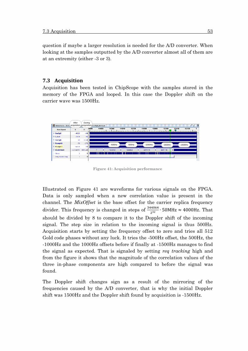
7.3 Acquisition 53
question if maybe a larger resolution is needed for the A/D converter. When looking at the samples outputted by the A/D converter almost all of them are at an extremity (either -3 or 3).
7.3 Acquisition Acquisition has been tested in ChipScope with the samples stored in the memory of the FPGA and looped. In this case the Doppler shift on the carrier wave was 1500Hz.
Figure 41: Acquisition performance
Illustrated on Figure 41 are waveforms for various signals on the FPGA. Data is only sampled when a new correlation value is present in the channel. The MixOffset is the base offset for the carrier replica frequency divider. This frequency is changed in steps of 344064
232∙ 50MHz ≈ 4000Hz. That
should be divided by 8 to compare it to the Doppler shift of the incoming signal. The step size in relation to the incoming signal is thus 500Hz. Acquisition starts by setting the frequency offset to zero and tries all 512 Gold code phases without any luck. It tries the -500Hz offset, the 500Hz, the -1000Hz and the 1000Hz offsets before if finally at -1500Hz manages to find the signal as expected. That is signaled by setting req tracking high and from the figure it shows that the magnitude of the correlation values of the three in-phase components are high compared to before the signal was found.
The Doppler shift changes sign as a result of the mirroring of the frequencies caused by the A/D converter, that is why the initial Doppler shift was 1500Hz and the Doppler shift found by acquisition is -1500Hz.
After acquisition
During acquisition
-500Hz 500Hz -1000Hz 1000Hz -1500Hz
Test results 54
7.4 Tracking The tracking algorithm has been tested with different Doppler shifts. A challenge is to both make the loop filter work with large frequency offsets, such as would be present just after acquisition is done and to keep it stable with only small variations in the frequency.
The next pages show some outputs from the tracking loop filter at different Doppler shifts. (10Hz and 60Hz Doppler shifts are in appendix). The figures to the left show the performance when using the frequencies that enable 8 samples per carrier wave period and the figures to the right show the performance when using the frequencies suggested in the previous report which make use of 4 samples per carrier wave period.
The figures showing the frequency offsets consist of the actual frequency offset (blue graph) and the average for the entire reading (red line). These values should ideally match the values of the actual Doppler shift. The figures with the carrier phase show the phase difference between the incoming carrier wave and the locally replicated carrier wave. Ideally this value should be zero.

7.4 Tracking 55
8 samples per period 4 samples per period
-100,0-75,0-50,0-25,0
0,025,050,075,0
100,0
f [Hz
]
T
Tracking 5 Hz Doppler shiftCarrier frequency offset
-100-75-50-25
0255075
100
f [Hz
]
T
Tracking 5 Hz Doppler shiftCarrier frequency offset
-90
-45
0
45
90
Offs
et [
Degr
ees]
T
Tracking 5 Hz Doppler shiftCarrier Phase
-90
-45
0
45
90
Offs
et [
Degr
ees]
T
Tracking 5 Hz Doppler shiftCarrier Phase
-100,0-75,0-50,0-25,0
0,025,050,075,0
100,0
f [Hz
]
T
Tracking 25 Hz Doppler shiftCarrier frequency offset
-100-75-50-25
0255075
100
f [Hz
]
T
Tracking 25 Hz Doppler shiftCarrier frequency offset
-90
-45
0
45
90
Offs
et [
Degr
ees]
T
Tracking 25 Hz Doppler shiftCarrier Phase
-90
-45
0
45
90
Offs
et [
Degr
ees]
T
Tracking 25 Hz Doppler shiftCarrier Phase
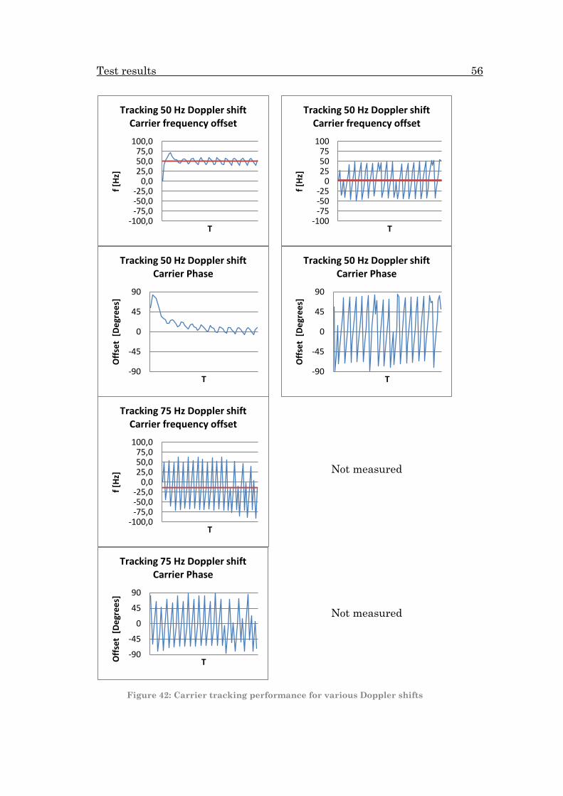
Test results 56
Not measured
Not measured
Figure 42: Carrier tracking performance for various Doppler shifts
-100,0-75,0-50,0-25,0
0,025,050,075,0
100,0
f [Hz
]
T
Tracking 50 Hz Doppler shiftCarrier frequency offset
-100-75-50-25
0255075
100
f [Hz
]
T
Tracking 50 Hz Doppler shiftCarrier frequency offset
-90
-45
0
45
90
Offs
et [
Degr
ees]
T
Tracking 50 Hz Doppler shiftCarrier Phase
-90
-45
0
45
90O
ffset
[De
gree
s]
T
Tracking 50 Hz Doppler shiftCarrier Phase
-100,0-75,0-50,0-25,0
0,025,050,075,0
100,0
f [Hz
]
T
Tracking 75 Hz Doppler shiftCarrier frequency offset
-90
-45
0
45
90
Offs
et [
Degr
ees]
T
Tracking 75 Hz Doppler shiftCarrier Phase
7.4 Tracking 57
The graphs clearly show that the 8 samples per period are vastly superior to the 4 samples. For all readings the phase difference is significantly lower for the 8 samples per period and it can track Doppler shifts over a greater span of frequencies.
With the settings used for the tests above, it is possible to track a carrier signal with an offset of up to at least 60Hz using 8 samples per period and up to at least 25Hz using 4 samples per period. Some frequencies seem to work better than others, this is partly incidental since the loop filter simply might get lucky and hit the right frequency and phase right away, but it also seems like high frequency offsets work better than low frequency offsets until a certain point where tracking is lost. Decreasing the gain of the loop filter output would make the fluctuations smaller for the small Doppler shifts, but it would also mean that the tracking could not work across as large a frequency range.
On the next page are test results for Gold code tracking. The blue graph is the discriminator output for a normalized discriminator. The discriminator is zero when the replicated Gold code is perfectly aligned with that of the incoming signal, which is the goal of the loop filter. Again readings are made for both the set of frequencies that enable 4 samples per carrier wave period and the ones enabling 8 samples per carrier wave period.
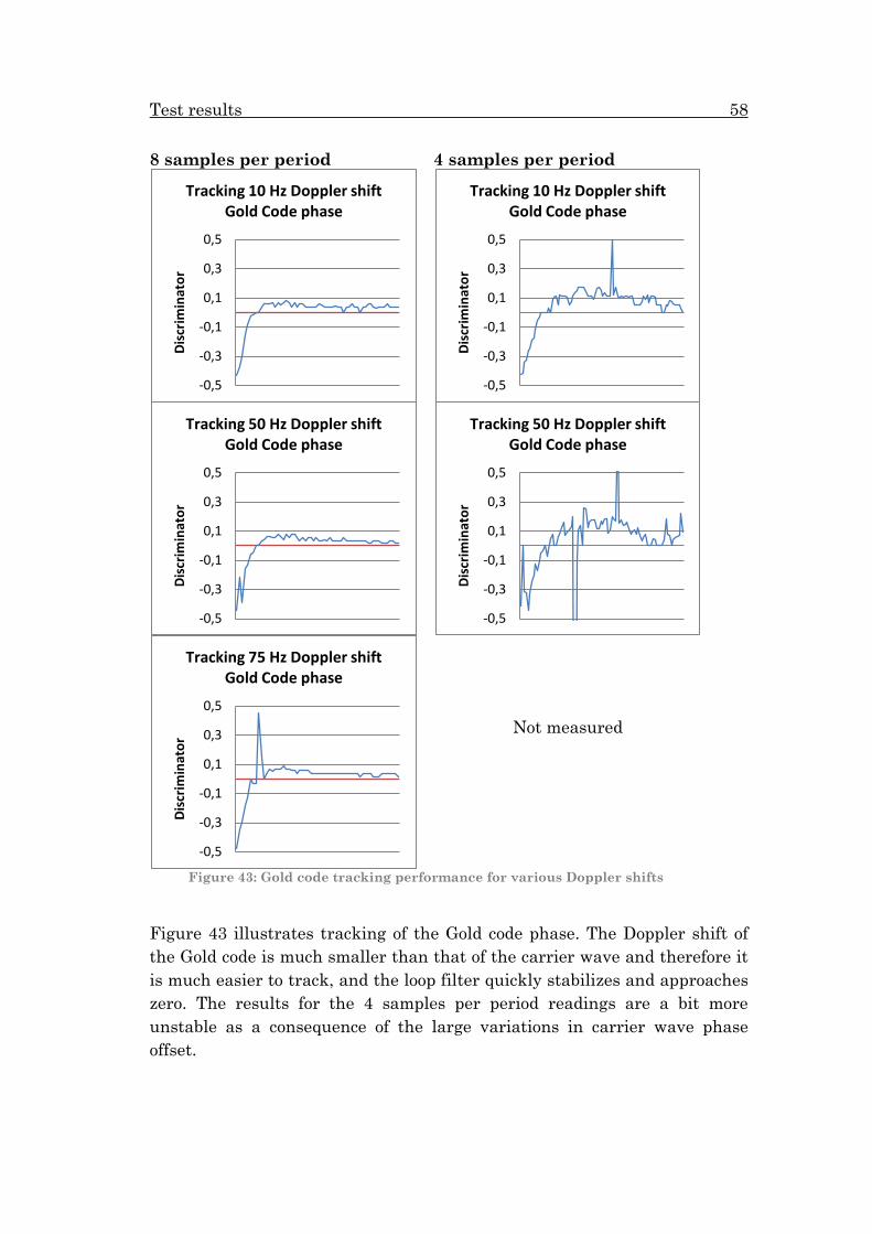
Test results 58
8 samples per period 4 samples per period
Not measured
Figure 43: Gold code tracking performance for various Doppler shifts
Figure 43 illustrates tracking of the Gold code phase. The Doppler shift of the Gold code is much smaller than that of the carrier wave and therefore it is much easier to track, and the loop filter quickly stabilizes and approaches zero. The results for the 4 samples per period readings are a bit more unstable as a consequence of the large variations in carrier wave phase offset.
-0,5
-0,3
-0,1
0,1
0,3
0,5
Disc
rimin
ator
Tracking 10 Hz Doppler shiftGold Code phase
-0,5
-0,3
-0,1
0,1
0,3
0,5
Disc
rimin
ator
Tracking 50 Hz Doppler shiftGold Code phase
-0,5
-0,3
-0,1
0,1
0,3
0,5
Disc
rimin
ator
Tracking 75 Hz Doppler shiftGold Code phase
-0,5
-0,3
-0,1
0,1
0,3
0,5
Disc
rimin
ator
Tracking 10 Hz Doppler shiftGold Code phase
-0,5
-0,3
-0,1
0,1
0,3
0,5Di
scrim
inat
or
Tracking 50 Hz Doppler shiftGold Code phase
Future work 59
8 Future work The implementation works, but there are some issues still to be dealt with. Especially the carrier tracking and the effects on the correlation values when many signals are received simultaneously give rise to concern.
Since the carrier tracking can only track a signal that is off by about 60Hz and the acquisition only gives a precision of 250Hz, there is an area in between that needs attention. It would seem that some extra acquisition is required to increase the precision from 250Hz and down to about 50Hz. It might also be possible to enhance the performance of the carrier loop filter, either by using the tan-1(Q/I) discriminator or by having the A/D converter sampling more samples per carrier period.
In regards to the decrease in correlation with more signals a possible solution would be to increase the resolution of the A/D converter, so that the incoming samples would not max out as often.
As it is now the method of transferring the decoded data further into the satellite is not implemented. Some communication protocol should be designed that ensures that the right data is sent at the right time. Furthermore flipping of the data stream is not implemented, which means that the decoder does not check to see if all the data is inverted. This feature could be implemented or it could be taken care of in the satellite computer or on the ground.

Conclusion 60
9 Conclusion A 32-channel parallel CDMA decoder has been implemented for an FPGA. An acquisition algorithm shared among the channels can successfully locate a signal with an unknown frequency and phase. A tracking algorithm has been showed to be able to lock on to the signal and adjust frequencies in order to keep the signals generated inside the FPGA synchronized with the incoming signal. The size of the implementation with 32 channels showed too large to fit on the Vitex-II FPGA used, but slightly larger FPGAs could contain it.

Bibliography 61
10 Bibliography
Borre, K, Akos, D, Bertelsen N, Rinder, P, Jensen, SH. 2007. A software-defined GPS and Galileo receiver - A single-frequency approach. s.l. : Birkhauser, 2007.
Chu, Pong P. 2008. FPGA Prototyping by VHDL examples. s.l. : WILEY INTERSCIENCE, 2008.
CubeSat. 2010. About us. [Online] July 19, 2010. [Cited: July 23, 2010.] http://www.cubesat.org/index.php/about-us.
Digilent. dpimref.vhd. Digilent. [Online] [Cited: July 30, 2010.] http://digilentinc.com/Data/Products/ADEPT/dpimref.vhd.
—. USB2 Accessory Board. Digilent. [Online] [Cited: July 30, 2010.] http://digilentinc.com/Products/Detail.cfm?NavPath=2,398,728&Prod=USB2.
DTUsat. 2010. Mission Definition Document. [Online] 2010. [Cited: July 23, 2010.] http://www.dtusat.dtu.dk/index.php?id=76.
Johansen, Teis. 2009. CDMA Decoder for DTUsat-II. s.l. : DTU, 2009.
Kaplan, Elliott D. & Hegarty, Christopher J. 1997. Understanding GPS principles and applications. s.l. : Artech House, 1997.
Poulsen, Ole Gammelgaard. 2009. Code Division Multiple Access Simulator for the DTUsat Bird-Satellite Radio Link. s.l. : DTU, 2009.
Wikipedia. 2010. Gold code. Wikipedia. [Online] June 4, 2010. [Cited: July 23, 2010.] http://en.wikipedia.org/wiki/Gold_code.
—. 2010. Linear feedback shift register. Wikipedia. [Online] July 27, 2010. [Cited: July 30, 2010.] http://en.wikipedia.org/wiki/Linear_feedback_shift_register.
—. 2010. Maximum length sequence. Wikipedia. [Online] July 8, 2010. [Cited: July 30, 2010.] http://en.wikipedia.org/wiki/Maximum_length_sequence.

Appendix 62
11 Appendix
Figure 44: Tracking loop filter performance at 10Hz Doppler shift
-100,0-75,0-50,0-25,0
0,025,050,075,0
100,0
f [Hz
]
T
Tracking 10 Hz Doppler shiftCarrier frequency offset
-100-75-50-25
0255075
100
f [Hz
]T
Tracking 10 Hz Doppler shiftCarrier frequency offset
-90
-45
0
45
90
Offs
et [
Degr
ees]
T
Tracking 10 Hz Doppler shiftCarrier Phase
-90
-45
0
45
90
Offs
et [
Degr
ees]
T
Tracking 10 Hz Doppler shiftCarrier Phase
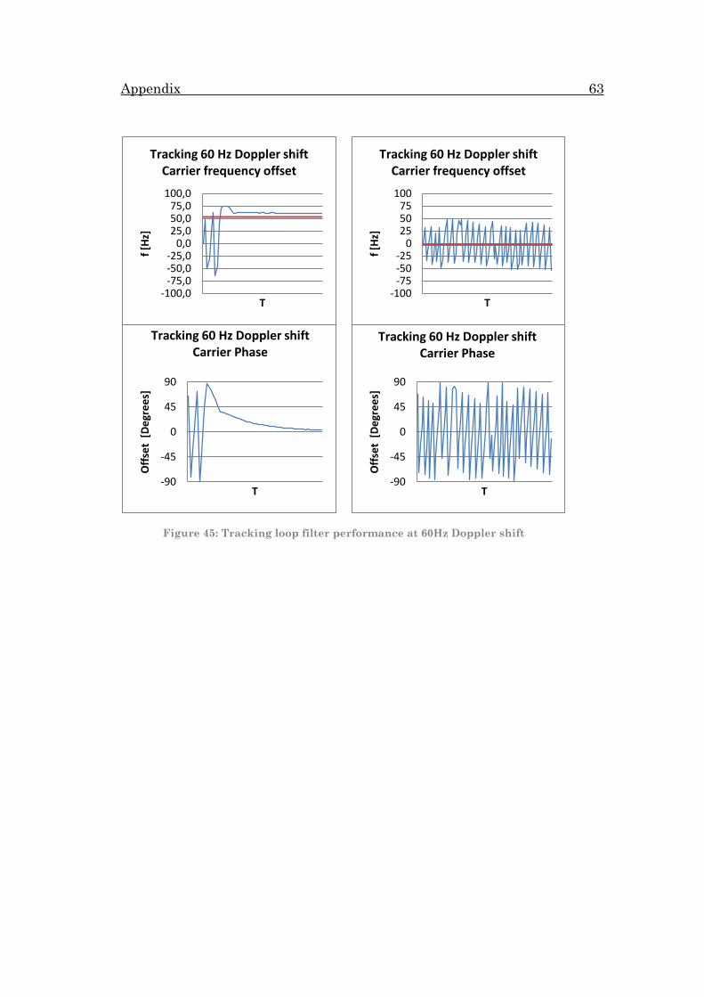
Appendix 63
Figure 45: Tracking loop filter performance at 60Hz Doppler shift
-100,0-75,0-50,0-25,0
0,025,050,075,0
100,0
f [Hz
]
T
Tracking 60 Hz Doppler shiftCarrier frequency offset
-100-75-50-25
0255075
100
f [Hz
]
T
Tracking 60 Hz Doppler shiftCarrier frequency offset
-90
-45
0
45
90
Offs
et [
Degr
ees]
T
Tracking 60 Hz Doppler shiftCarrier Phase
-90
-45
0
45
90O
ffset
[De
gree
s]
T
Tracking 60 Hz Doppler shiftCarrier Phase


