For the information for microcontroller supports, see the following web site.
http://edevice.fujitsu.com/micom/en-support/
32-bit RISC MicrocontrollerCMOS
FR30 MB91101 Series
MB91101A
DESCRIPTIONThe MB91101 Series is a standard single-chip microcontroller constructed around the 32-bit RISC CPU (FR*family) core with abundant I/O resources and bus control functions optimized for high-performance/high-speedCPU processing for embedded controller applications. To support the vast memory space accessed by the 32-bit CPU, the MB91101A Series normally operates in the external bus access mode and executes instructionson the internal 1 Kbyte cache memory and 2 Kbytes RAM for enhanced performance.
The MB91101A Series is optimized for applications requiring high-performance CPU processing such as navi-gation systems, high-performance FAXs and printer controllers.
*: FR, the abbreviation of FUJITSU RISC controller, is a line of products of Fujitsu Mictoelectronics Limited.
FEATURESFR CPU• 32-bit RISC, load/store architecture, 5-stage pipeline• Operating clock frequency: Internal 50 MHz/external 25 MHz (PLL used at source oscillation 12.5 MHz)• General purpose registers: 32 bits × 16• 16-bit fixed length instructions (basic instructions), 1 instruction/1 cycle• Memory to memory transfer, bit processing, barrel shifter processing: Optimized for embedded applications• Function entrance/exit instructions, multiple load/store instructions of register contents, instruction systems
supporting high level languages• Register interlock functions, efficient assembly language coding• Branch instructions with delay slots: Reduced overhead time in branch executions
• Interrupt (push PC and PS): 6 cycles, 16 priority levels
External bus interface• Clock doubler: Internal 50 MHz, external bus 25 MHz operation• 25-bit address bus (32 Mbytes memory space)• 8/16-bit data bus• Basic external bus cycle: 2 clock cycles• Chip select outputs for setting down to a minimum memory block size of 64 Kbytes: 6• Interface supported for various memory technologies
DRAM interface (area 4 and 5)• Automatic wait cycle insertion: Flexible setting, from 0 to 7 for each area• Unused data/address pins can be configured as input/output ports.• Little endian mode supported (Select 1 area from area 1 to 5)
DRAM interface• 2 banks independent control (area 4 and 5)• Normal mode (double CAS DRAM)/high-speed page mode (single CAS DRAM)/Hyper DRAM• Basic bus cycle: Normally 5 cycles, 2-cycle access possible in high-speed page mode• Programmable waveform: Automatic 1-cycle wait insertion to RAS and CAS cycles• DRAM refresh
CBR refresh (interval time configurable by 6-bit timer)Self-refresh mode
Cache memory• 1-Kbyte instruction cache memory• 32 block/way, 4 entry(4 word)/block• 2 way set associative• Lock function: For specific program code to be resident in cashe memory
DMA controller (DMAC)• 8 channels• Transfer incident/external pins/internal resource interrupt requests• Transfer sequence: Step transfer/block transfer/burst transfer/continuous transfer• Transfer data length: 8 bits/16 bits/32 bits selective• NMI/interrupt request enables temporary stop operation.
UART• 3 independent channels• Full-duplex double buffer• Data length: 7 bits to 9 bits (non-parity), 6 bits to 8 bits (parity)• Asynchronous (start-stop system), CLK-synchronized communication selective• Multi-processor mode• Internal 16-bit timer (U-TIMER) operating as a proprietary baud rate generator: Generates any given baud rate• External clock can be used as a transfer clock.• Error detection: Parity, frame, overrun
(Continued)
2 DS07-16301-5E
MB91101 Series
(Continued)
10-bit A/D converter (successive approximation conversion type)• 10-bit resolution, 4 channels• Successive approximation type: Conversion time of 5.6 µs at 25 MHz• Internal sample and hold circuit• Conversion mode: Single conversion/scanning conversion/repeated conversion/stop conversion selective• Start: Software/external trigger/internal timer selective
Gear function: Operating clocks for CPU and peripherals are independently selective.Gear clock can be selected from 1/1, 1/2, 1/4 and 1/8 (or 1/2, 1/4, 1/8 and 1/16).However, operating frequency for peripherals is less than 25 MHz.
• Packages: LQFP-100 and QFP-100• CMOS technology (0.35 µm)• Power supply voltage
5 V: CPU power supply 5.0 V ±10% (internal regulator)A/D power supply 2.7 V to 3.6 V
3 V: CPU power supply 2.7 V to 3.6 V (without internal regulator)A/D power supply 2.7 V to 3.6 V
P20 to P27Can be configured as I/O ports when external data bus width is set to 8-bit.
33 to 39,41
36 to 42,44
D24 to D30,D31
C Bit 24 to bit 31 of external data bus
42,44 to 58
45,47 to 61
A00,A01 to A15
F Bit 00 to bit 15 of external address bus
59 to 64,66,67
62 to 67,69,70
A16 to A21,A22,A23
F
Bit 16 to bit 23 of external address bus
P60 to P65,P66,P67
Can be configured as I/O ports when not used as address bus.
68 71A24
LBit 24 of external address bus
EOP0Can be configured as DMAC EOP output (ch. 0) when DMAC EOP output is enabled.
19 22RDY
CExternal ready inputInputs “0” when bus cycle is being executed and not completed.
P80 Can be configured as a port when RDY is not used.
20 23BGRNT
FExternal bus release acknowledge outputOutputs “L” level when external bus is released.
P81 Can be configured as a port when BGRNT is not used.
21 24BRQ
CExternal bus release request inputInputs “1” when release of external bus is required.
P82 Can be configured as a port when BRQ is not used.
22 25 RD L Read strobe output pin for external bus
23 26 WR0 L
Write strobe output pin for external busRelation between control signals and effective byte locations is as follows:
WR1 is High-Z during resetting.Attach an external pull-up resister when using at 16-bit bus width.
24 27WR1
F
P85 Can be configured as a port when WR1 is not used.
16-bit bus width 8-bit bus width
D15 to D08 WR0 WR0
D07 to D00 WR1 (I/O port enabled)
6 DS07-16301-5E
MB91101 Series
*1: FPT-100P-M20
*2: FPT-100P-M06(Continued)
Pin no. Pin name Circuit
type DescriptionLQFP*1 QFP*2
11 14 CS0 L Chip select 0 output (“L” active)
10 13CS1
FChip select 1 output (“L” active)
PA1 Can be configured as a port when CS1 is not used.
9 12CS2
FChip select 2 output (“L” active)
PA2 Can be configured as a port when CS2 is not used.
8 11
CS3
F
Chip select 3 output (“L” active)
PA3 Can be configured as a port when CS3 and EOP1 are not used.
EOP1EOP output pin for DMAC (ch. 1)This function is available when EOP output for DMAC is en-abled.
7 10CS4
FChip select 4 output (“L” active)
PA4 Can be configured as a port when CS4 is not used.
6 9CS5
FChip select 5 output (“L” active)
PA5 Can be configured as a port when CS5 is not used.
5 8CLK
FSystem clock outputOutputs clock signal of external bus operating frequency.
PA6 Can be configured as a port when CLK is not used.
96 99RAS0
FRAS output for DRAM bank 0Refer to the DRAM interface for details.
PB0 Can be configured as a port when RAS0 is not used.
97 100CS0L
FCASL output for DRAM bank 0Refer to the DRAM interface for details.
PB1 Can be configured as a port when CS0L is not used.
98 1CS0H
FCASH output for DRAM bank 0Refer to the DRAM interface for details.
PB2 Can be configured as a port when CS0H is not used.
99 2DW0
FWE output for DRAM bank 0 (“L” active)Refer to the DRAM interface for details.
PB3 Can be configured as a port when DW0 is not used.
100 3
RAS1
F
RAS output for DRAM bank 1Refer to the DRAM interface for details.
PB4Can be configured as a port when RAS1 and EOP2 are not used.
EOP2DMAC EOP output (ch. 2)This function is available when DMAC EOP output is enabled.
DS07-16301-5E 7
MB91101 Series
*1: FPT-100P-M20
*2: FPT-100P-M06(Continued)
Pin no. Pin name Circuit
type DescriptionLQFP*1 QFP*2
1 4
CS1L
F
CASL output for DRAM bank 1Refer to the DRAM interface for details.
PB5 Can be configured as a port when CS1L and DREQ2 are not used.
DREQ2
External transfer request input pin for DMAThis pin is used for input when external trigger is selected to cause DMAC operation, and it is necessary to disable output for other functions from this pin unless such output is made intentionally.
2 5
CS1H
F
CASH output for DRAM bank 1Refer to the DRAM interface for details.
PB6 Can be configured as a port when CS1H and DACK2 are not used.
DACK2External transfer request acknowledge output pin for DMAC (ch. 2)This function is available when transfer request output for DMAC is enabled.
3 6DW1
FWE output for DRAM bank 1 (“L” active)Refer to the DRAM interface for details.
PB7 Can be configured as a port when DW1 is not used.
16 to 18 19 to 21MD0 to
MD2G
Mode pins 0 to 2MCU basic operation mode is set by these pins.Directly connect these pins with VCC or VSS for use.
External interrupt request input pinsThese pins are used for input during corresponding interrupt is en-abled, and it is necessary to disable output for other functions from these pins unless such output is made intentionally.
PE0,PE1
Can be configured as I/O ports when INT0, INT1 are not used.
89 92
INT2
F
External interrupt request input pinThis pin is used for input during corresponding interrupt is enabled, and it is necessary to disable output for other functions from this pin unless such output is made intentionally.
SC1Clock I/O pin for UART1Clock output is available when clock output of UART1 is enabled.
PE2Can be configured as the I/O port when INT2 and SC1 are not used.This function is available when UART1 clock output is disabled.
8 DS07-16301-5E
MB91101 Series
*1: FPT-100P-M20
*2: FPT-100P-M06(Continued)
Pin no. Pin name Circuit
type DescriptionLQFP*1 QFP*2
88 91
INT3
F
External interrupt request input pinThis pin is used for input during corresponding interrupt is enabled, and it is necessary to disable output for other functions from this pin unless such output is made intentionally.
SC2UART2 clock I/O pinClock output is available when UART2 clock output is enabled.
PE3Can be configured as the I/O port when INT3 and SC2 are not used.This function is available when UART2 clock output is disabled.
87,86
90,89
DREQ0,DREQ1
F
External transfer request input pins for DMAThese pins are used for input when external trigger is selected to cause DMAC operation, and it is necessary to disable output for other functions from these pins unless such output is made inten-tionally.
PE4,PE5
Can be configured as I/O ports when DREQ0, DREQ1 are not used.
85 88
DACK0
F
External transfer request acknowledge output pin for DMAC (ch. 0)This function is available when transfer request output for DMAC is enabled.
PE6Can be configured as the I/O port when DACK0 is not used.This function is available when transfer request acknowledge out-put for DMAC or DACK0 output is disabled.
84 87
DACK1
F
External transfer request acknowledge output pin for DMAC (ch. 1)This function is available when transfer request output for DMAC is enabled.
PE7Can be configured as the I/O port when DACK1 is not used.This function is available when transfer request output for DMAC or DACK1 output is disabled.
76 79
SI0
F
UART0 data input pinThis pin is used for input during UART0 is in input operation, and it is necessary to disable output for other functions from this pin un-less such output is made intentionally.
TRG0
PWM timer external trigger input pinThis pin is used for input during PWM timer external trigger is in in-put operation, and it is necessary to disable output for other func-tions from this pin unless such output is made intentionally.
PF0 Can be configured as the I/O port when SI0 and TRG0 are not used.
DS07-16301-5E 9
MB91101 Series
*1: FPT-100P-M20
*2: FPT-100P-M06(Continued)
Pin no. Pin name Circuit
type DescriptionLQFP*1 QFP*2
77 80
SO0
F
UART0 data output pinThis function is available when UART0 data output is enabled.
TRG1PWM timer external trigger input pinThis function is available when serial data output of PF1, UART0 are disabled.
PF1
Can be configured as the I/O port when SO0 and TRG1 are not used.This function is available when serial data output of UART0 is dis-abled.
78 81
SC0
F
UART0 clock I/O pin Clock output is available when UART0 clock output is enabled.
OCPA3PWM timer output pinThis function is available when PWM timer output is enabled.
PF2Can be configured as the I/O port when SC0 and OCPA3 are not used.This function is available when UART0 clock output is disabled.
79 82
SI1
F
UART1 data input pinThis pin is used for input during UART1 is in input operation, and it is necessary to disable output for other functions from this pin un-less such output is made intentionally.
TRG2
PWM timer external trigger input pinThis pin is used for input during PWM timer external trigger is in in-put operation, and it is necessary to disable output for other func-tions from this pin unless such output is made intentionally.
PF3 Can be configured as the I/O port when SI1 and TRG2 are not used.
80 83
SO1
F
UART1 data output pinThis function is available when UART1 data output is enabled.
TRG3PWM timer external trigger input pin This function is available when PF4, UART1 data outputs are dis-abled.
PF4Can be configured as the I/O port when SO1 and TRG3 are not used.This function is available when UART1 data output is disabled.
81 84
SI2
F
UART2 data input pinThis pin is used for input during UART2 is in input operation, and it is necessary to disable output for other functions from this pin un-less such output is made intentionally.
OCPA1PWM timer output pinThis function is available when PWM timer output is enabled.
PF5Can be configured as the I/O port when SI2 and OCPA1 are not used.
10 DS07-16301-5E
MB91101 Series
(Continued)
*1: FPT-100P-M20
*2: FPT-100P-M06
Note: In most of the above pins, I/O ports and resource I/O are multiplexed, e.g. P82 and BRQ. In case of conflictbetween output of I/O ports and resource I/O, priority is always given to the output of resource I/O.
Pin no. Pin name Circuit
type DescriptionLQFP*1 QFP*2
82 85
SO2
F
UART2 data output pinThis function is available when UART2 data output is enabled.
OCPA2PWM timer output pinThis function is available when PWM timer output is enabled.
PF6Can be configured as the I/O port when SO2 and OCPA2 are not used.This function is available when UART2 data output is disabled.
83 86
OCPA0
F
PWM timer output pinThis function is available when PWM timer output is enabled.
PF7Can be configured as the I/O port when OCPA0 and ATG are not used.This function is available when PWM timer output is disabled.
ATG
External trigger input pin for A/D converterThis pin is used for input when external trigger is selected to cause A/D converter operation, and it is necessary to disable output for other functions from this pin unless such output is made intentionally.
72 to 75 75 to 78 AN0 to AN3 D Analog input pins of A/D converter
69 72 AVCC — Power supply pin (VCC) for A/D converter
70 73 AVRH —Reference voltage input (high) for A/D converterMake sure to turn on and off this pin with potential of AVRH or more applied to AVCC.
71 74 AVSS / AVRL —Power supply pin (VSS) for A/D converter and reference voltage input pin (low)
43,93
46,96
VCC5 —5 V power supply pin (VCC) for digital circuitAlways two pins must be connected to the power supply (con-nect to 3 V power supply when operating at 3 V).
4 7 VCC3 —Bypass capacitor pin for internal capacitor.Also connect this pin to 3 V power supply when operating at 3 V.
15,40,65,90
18,43,68,93
VSS — Earth level (VSS) for digital circuit
DS07-16301-5E 11
MB91101 Series
DRAM CONTROL PIN
Pin nameData bus 16-bit mode Data bus 8-bit mode
Remarks2CAS/1WR mode 1CAS/2WR mode —
RAS0 Area 4 RAS Area 4 RAS Area 4 RASCorrespondence of “L”, “H” to lower address 1 bit (A0) in data bus 16-bit mode“L”: “0”“H”: “1”CASL:CAS which A0 corresponds to “0” areaCASH:CAS which A0 corresponds to “1” areaWEL: WE which A0 cor-responds to “0” areaWEH:WE which A0 cor-responds to “1” area
RAS1 Area 5 RAS Area 5 RAS Area 5 RAS
CS0L Area 4 CASL Area 4 CAS Area 4 CAS
CS0H Area 4 CASH Area 4 WEL Area 4 CAS
CS1L Area 5 CASL Area 5 CAS Area 5 CAS
CS1H Area 5 CASH Area 5 WEL Area 5 CAS
DW0 Area 4 WE Area 4 WEH Area 4 WE
DW1 Area 5 WE Area 5 WEH Area 5 WE
12 DS07-16301-5E
MB91101 Series
I/O CIRCUIT TYPE
(Continued)
Type Circuit Remarks
A
• Oscillation feedback resistance 1 MΩapprox.With standby control
• CMOS level Hysteresis inputWithout standby control
L
• CMOS level output
R
P-ch
N-ch
Standby control signal
Digital input
Digital output
Digital output
R
P-ch
N-ch
Digital input
R
P-ch
N-ch
Digital input
P-ch
N-ch Digital output
Digital output
14 DS07-16301-5E
MB91101 Series
HANDLING DEVICES 1. Preventing Latchup
In CMOS ICs, applying voltage higher than VCC or lower than VSS to input/output pin or applying voltage overrating across VCC and VSS may cause latchup. This phenomenon rapidly increases the power supply current, which may result in thermal breakdown of thedevice. Make sure to prevent the voltage from exceeding the maximum rating.Take care that the analog power supply (AVCC, AVRH) and the analog input do not exceed the digital powersupply (VCC) when the analog power supply turned on or off.
2. Treatment of Unused Pins
Unused pins left open may cause malfunctions. Make sure to connect them to pull-up or pull-down resistors.
3. External Reset Input
It takes at least 5 machine cycle to input “L” level to the RST pin and to ensure inner reset operation properly.
4. Remarks for External Clock Operation
When external clock is selected, supply it to X0 pin generally, and simultaneously the opposite phase clock toX0 must be supplied to X1 pin. However, in this case the stop mode must not be used (because X1 pin stopsat “H” output in stop mode).And it can be used to supply only to X0 pin with 5 V power supply at 12.5 MHz and less than.
5. Power Supply Pins
When there are several VCC and VSS pins, each of them is equipotentially connected to its counterpart inside ofthe device, minimizing the risk of malfunctions such as latch up. To further reduce the risk of malfunctions, toprevent EMI radiation, to prevent strobe signal malfunction resulting from creeping-up of ground level and toobserve the total output current standard, connect all VCC and VSS pins to the power supply or GND.It is preferred to connect VCC and VSS of the MB91101 Series to power supply with minimal impedance possible.It is also recommended to connect a ceramic capacitor as a bypass capacitor of about 0.1 µF between VCC andVSS at a position as close as possible to the MB91101 Series.
X0
X1OpenMB91101 Series
X0
X1MB91101 Series
Using an external clock (normal)Note: Stop mode (oscillation stop mode) can not be used.
Using an external clock (can be used at 12.5 MHz and less than.)
(5 V power supply only)
• Using an external clock
DS07-16301-5E 15
MB91101 Series
The MB91101 Series has an internal regulator. When using with 5 V power supply, supply 5 V to VCC5 pin andmake sure to connect about 0.1 µF bypass capacitor to VCC3 pin for regulator. And another 3 V power supply isneeded for the A/D convertor. When using with 3 V power supply, connect both VCC5 pin and VCC3 pin to the 3V power supply.
6. Crystal Oscillator Circuit
Noises around X0 and X1 pins may cause the malfunction of the MB91101 Series. In designing the PC board,layout X0 and X1 pins, crystal oscillator (or ceramic oscillator) and bypass capacitor for grounding as close aspossible. It is strongly recommended to design PC board so that X1 and X0 pins are surrounded by grounding area forstable operation.
7. Turning-on Sequence of A/D Converter Power Supply and Analog Input
Make sure to turn on the digital power supply (VCC) before turning on the A/D converter (AVCC, AVRH) andapplying voltage to analog input (AN0 to AN3).Make sure to turn off digital power supply after power supply to A/D converters and analog inputs have beenswitched off. (There are no such limitations in turning on power supplies. Analog and digital power supplies maybe turned on simultaneously.) Make sure that AVRH never exceeds AVCC when turning on/off power supplies.
8. Fluctuation of Power Supply Voltage
Warranty range for normal operation against fluctuation of power supply voltage VCC is as given in rating. However,sudden fluctuation of power supply voltage within the warranty range may cause malfunctions. It is recommendedto make every effort to stabilize the power supply voltage to IC. It is also recommended that by controlling powersupply as a reference of stabilizing, VCC ripple fluctuation (P-P value) at the commercial frequency (50 Hz to 60 Hz) should be less than 10% of the standard VCC value and the transient regulation should be less than 0.1 V/ms at instantaneous deviation like turning off the power supply.
9. Mode Setting Pins (MD0 to MD2)
Connect mode setting pins (MD0 to MD2) directly to VCC or VSS.Arrange each mode setting pin and VCC or VSS patterns on the printed circuit board as close as possible andmake the impedance between them minimal to prevent mistaken entrance to the test mode caused by noises.
10. Internal DC Regulator
Internal DC regulator stops in stop mode. When the regulator stops owing to the increase of inner leakagecurrent (ICCH) in stop mode, malfunction caused by noise or any troubles about power supply in normal oper-ation, the internal 3 V power supply voltage may decrease less than the warranty range for normal operation.So when using the internal regulator and stop mode with 5 V power supply, never fail to support externally sothat 3 V power supply voltage might not decrease. However, even in such a case, the internal regulator can be
• Connecting to a power supply
VCC5
AVCC
AVRH
AVSS
VSS
VCC35 V
GND
[Using with 5 V power supply]
VCC5
AVCC
AVRH
AVSS
VSS
VCC3
3 V
3 V
GND
[Using with 3 V power supply]
About0.1 µF
16 DS07-16301-5E
MB91101 Series
restarted by inputting the reset procedure. (In this case, set the reset to “L” level within the oscillation stabilizingwaiting time.)
11. Pin Condition at Turning on the Power Supply
The pin condition at turning on the power supply is unstable. The circuit starts being initialized after turning onthe power supply and then starting oscillation and then the operation of the internal regulator becomes stable.So it takes about 42 ms for the pin to be initialized from the oscillation starting at the source oscillation 12.5 MHz.Take care that the pin condition may be output condition at initial unstable condition.(With the MB91101A, however, initalization can be achieved in less than about 42 ms after turning on the internalpower supply by maintaining the RST pin at "L" level.)
12. Source Oscillation Input at Turning on the Power Supply
At turning on the power supply, never fail to input the clock before cancellation of the oscillation stabilizing waiting.
13. Hardware Stand-by at Turning on the Power Supply
When turning on the power supply with the HST pin being set to “L” level, the hardware does not stand by.However the HST pin becomes available after the reset cancellation, the HST pin must once be back to “H” level.
14. Power on Reset
Make sure to make power on reset at turning on the power supply or returning on the power supply when thepower supply voltage is below the warranty range for normal operation.
15. Notes on during operation of PLL clock mode
If the PLL clock mode is selected, the microcontroller attempt to be working with the self oscillating circuit evevnwhen there is no external oscillator or external clock input is stopped. Performance of this operation, however,cannot be guaranteed.
16. Watchdog timer function
The watchdog timer supported by the FR family monitors the program that performs the reset delay operationfor a specified time. If the program hangs up and the reset delay operation is not performed, the watchdog timerresets the CPU. Therefore, once the watchdog timer is enabled, operation continues until the CPU is reset.As an exception, a reset delay automatically occurs if the CPU stops program execution.
VCC5
VCC3
VSS
3.6 kΩ
6.8 kΩ0.1 µF approx.
5 V
• Using STOP mode with 5 V power supply
DS07-16301-5E 17
MB91101 Series
BLOCK DIAGRAM
AN0 to AN3AVCC
AVSS /AVRLAVRH
Bit search module Instruction cache (1 Kbyte)
D-b
us (
32 b
its)
I-bu
s (1
6 bi
ts)
C-b
us (
32 b
its)
R-b
us (
16 b
its)
Clock control unit(Watchdog timer)
Interrupt control unit
10-bit A/D converter(4 ch.)
Reload timer (3 ch.)
Port
Bus converter (32 bits↔16 bits)
DRAM controller
Port 0 to port B
UART (3 ch.)(Baud rate timer)
Bus controller
DMA controller (DMAC) (8 ch.)
Bus converter(Harvard↔Princeton)
RAM (2 Kbytes)
PWM timer (4 ch.)
FR CPU
X0X1RSTHST
DREQ0 to DREQ2 DACK0 to DACK2EOP0 to EOP2
D16 to D31A00 to A24RDWR0, WR1RDYCLKCS0 to CS5BRQBGRNT
SI0 to SI2SO0 to SO2SC0 to SC2
OCPA0 to OCPA3TRG0 to TRG3
INT0 to INT3NMI
ATG
4
4
3
3
3
44
RAS0RAS1CS0LCS0HCS1LCS1HDW0DW1
6
33
2
2516
MD0 to MD2, P20 to P27, P60 to P67,P80 to P82, P85, PA1 to PA6,PB0 to PB7, PE0 to PE7, PF0 to PF7,VCC3, VCC5, VSS
Other pins
Note: Pins are display for functions (Actually some pins are multiplexer).When using REALOS, time control should be done by using external interrupt or inner timer.
18 DS07-16301-5E
MB91101 Series
CPU CORE1. Memory Space
The FR family has a logical address space of 4 Gbytes (232 addesses) and the CPU linearly accesses the memory
space.
• Direct addressing area
The following areas on the memory space are assigned to direct addressing area for I/O. In these areas, anaddress can be specified in a direct operand of a code.
Direct areas consists of the following areas dependent on accessible data sizes.
Byte data access: 000H to 0FFH
Half word data access: 000H to 1FFH
Word data access: 000H to 3FFH
• Memory space
I/O area
I/O area
Access inhibited
Access inhibited
External area
Direct addressing area
See “ I/O MAP”
0000 0000H
0000 0400H
0000 0800H
0001 0000H
FFFF FFFFH
External ROM/external bus mode
Embedded RAM
0000 1800H
0000 1000H
Address
DS07-16301-5E 19
MB91101 Series
2. Registers
The FR family has two types of registers; dedicated registers embedded on the CPU and general-purposeregisters on memory.
• Dedicated registersProgram counter (PC): 32-bit length, indicates the location of the instruction to be executed.Program status (PS): 32-bit length, register for storing register pointer or condition codesTable base register (TBR): Holds top address of vector table used in EIT (Exceptional/Interrupt/Trap)
processing.Return pointer (RP): Holds address to resume operation after returning from a subroutine.System stack pointer (SSP): Indicates system stack space.User's stack pointer (USP): Indicates user’s stack space.Multiplication/division result register (MDH/MDL): 32-bit length, register for multiplication/division
• Program status (PS)
The PS register is for holding program status and consists of a condition code register (CCR), a system conditioncode register (SCR) and an interrupt level mask register (ILM).
PC
PS
TBR
RP
SSP
USP
MDH
MDL
Program counter
Program status
Table base register
Return pointer
System stack pointer
User’s stack pointer
Multiplication/division result register
Indeterminate
Indeterminate
Indeterminate
Indeterminate
Indeterminate
32 bitsXXXX XXXXH
000F FC00H
XXXX XXXXH
0000 0000 H
XXXX XXXXH
XXXX XXXXH
XXXX XXXXH
Initial value
— ILM4 ILM3 ILM2 ILM1 —ILM0 D1 D0 T — S— Z CVNI
31 to 21 20 19 18 17 15 to 1116 10 9 8 7 56 2 0134
ILM SCR CCR
PS
20 DS07-16301-5E
MB91101 Series
• Condition code register (CCR)
S-flag: Specifies a stack pointer used as R15.I-flag: Controls user interrupt request enable/disable.N-flag: Indicates sign bit when division result is assumed to be in the 2’s complement format.Z-flag: Indicates whether or not the result of division was “0”.V-flag: Assumes the operand used in calculation in the 2’s complement format and indicates whether or not
overflow has occurred.C-flag: Indicates if a carry or borrow from the MSB has occurred.
• System condition code register (SCR)
T-flag: Specifies whether or not to enable step trace trap.• Interrupt level mask register (ILM)
ILM4 to ILM0:Register for holding interrupt level mask value. The value held by this register is used as a level mask. When an interrupt request issued to the CPU is higher than the level held by ILM, the interrupt request is accepted.
ILM4 ILM3 ILM2 ILM1 ILM0 Interrupt level High-low
0 0 0 0 0 0 High
::
::
0 1 0 0 0 15
::
::
1 1 1 1 1 31 Low
DS07-16301-5E 21
MB91101 Series
GENERAL-PURPOSE REGISTERSR0 to R15 are general-purpose registers embedded on the CPU. These registers functions as an accumulatorand a memory access pointer (field for indicating address).
Of the above 16 registers, following registers have special functions. To support the special functions, part ofthe instruction set has been sophisticated to have enhanced functions.
Delayed interrupt cause bit 63 3F ICR47 300H 000FFF00H
34 DS07-16301-5E
MB91101 Series
(Continued)
*: REALOS/FR uses interrupt number 0x40 and 0x41 for system code.
Interrupt causesInterrupt number Interrupt level TBR default
addressDecimal Hexadecimal Register Offset
System reserved (used in REALOS*) 64 40 — 2FCH 000FFEFCH
System reserved (used in REALOS*) 65 41 — 2F8H 000FFEF8H
Used in INT instructions66to
255
42toFF
—2F4H
to000H
000FFEF4H
to000FFC00H
DS07-16301-5E 35
MB91101 Series
PERIPHERAL RESOURCES1. I/O Ports
There are 2 types of I/O port register structure; port data register (PDR0 to PDRF) and data direction register(DDR0 to DDRF), where bits PDR0 to PDRF and bits DDR0 to DDRF corresponds respectively. Each bit onthe register corresponds to an external pin. In port registers input/output register of the port configures input/output function of the port, while corresponding bit (pin) configures input/output function in data direction regis-ters. Bit “0” specifies input and “1” specifies output.
•For input (DDR = “0”) setting;PDR reading operation: reads level of corresponding external pin.PDR writing operation: writes setting value to PDR.
•For output (DDR = “1”) setting;PDR reading operation: reads PDR value.PDR writing operation: outputs PDR value to corresponding external pin.
•Block diagram
PDR
DDR
(Port data register)
(Data direction register)
Resource output enable
Resource output 1
0
1
0
PDR read
Resource input
Pin
Dat
a bu
s
36 DS07-16301-5E
MB91101 Series
( )W–
• Port data register
• Data direction register
bit 7 bit 0000001H
000005H
00000BH
000009H
000008H
000012H
000013H
Address Initial value
:Access:Readable and writable:Indeterminate
(R/W)
(R/W)
(R/W)
(R/W)
(R/W)
(R/W)
(R/W)
PDR2
PDR6
PDR8
PDRA
PDRB
PDRE
PDRF
( )R/WX
bit 7 bit 0000601H
000605H
00060BH
000609H
000608H
0000D2H
0000D3H
0 0 0 0 0 0 0 0B
0 0 0 0 0 0 0 0B
- - 0 - - 0 0 0B
- 0 0 0 0 0 0 -B
0 0 0 0 0 0 0 0B
0 0 0 0 0 0 0 0B
0 0 0 0 0 0 0 0B
Address Initial value
:Access:Write only:Unused
(W)
(W)
(W)
(W)
(W)
(W)
(W)
DDR2
DDR6
DDR8
DDRA
DDRB
DDRE
DDRF
XXXXXXXXB
XXXXXXXXB
- - X - - XXXB
- XXXXXX -B
XXXXXXXXB
XXXXXXXXB
XXXXXXXXB
DS07-16301-5E 37
MB91101 Series
2. DMA Controller (DMAC)
The DMA controller is a module embedded in FR family devices, and performs DMA (direct memory access)transfer.
DMA transfer performed by the DMA controller transfers data without intervention of CPU, contributing to en-hanced performance of the system.• 8 channels• Mode: single/block transfer, burst transfer and continuous transfer: 3 kinds of transfer• Transfer all through the area• Max 65536 of transfer cycles• Interrupt function right after the transfer• Selectable for address transfer increase/decrease by the software• External transfer request input pin, external transfer request accept output pin, external transfer complete
output pin: three pins for each
• Block diagram
Sequencer
Edge/leveldetection circuit
Internal resourceTransfer request
DREQ0 to DREQ2 DACK0 to DACK2
EOP0 to EOP2
Interrupt request
Data buffer Switcher
DPDP
DACSR
DATCR Dat
a bu
s
Mode
BLK DEC
INC / DEC
BLK
DMACT
SADR
DADR
3 3 3
3
8
5
38 DS07-16301-5E
MB91101 Series
• Registers (DMAC internal registers)
• Registers (DMA descriptor)
bit 31 bit 0
00000200H
00000201H
00000202H
00000203H
00000204H
00000205H
00000206H
00000207H
00000208H
00000209H
0000020AH
0000020BH
XXXXXXXXB
XXXXXXXXB
XXXXXXXXB
X 0 0 0 0 0 0 0B
0 0 0 0 0 0 0 0B
0 0 0 0 0 0 0 0B
0 0 0 0 0 0 0 0B
0 0 0 0 0 0 0 0B
XXXXXXXXB
XXXX 0 0 0 0B
XXXX 0 0 0 0B
XXXX 0 0 0 0B
Address Initial value
:Access:Readable and writable:Indeterminate
DPDP
( )R/WX
bit 16
DACSR
DATCR
(R/W)
(R/W)
(R/W)
bit 31 bit 0
DPDP + 0H
DPDP + 0CH
DPDP + 54H
DMAch.0DescriptorDMAch.1Descriptor
DMAch.7Descriptor
Address
DS07-16301-5E 39
MB91101 Series
3. UART
The UART is a serial I/O port for supporting asynchronous (start-stop system) communication or CLK synchro-nous communication, and it has the following features.
The MB91101 Series consists of 3 channels of UART.
• Full-duplex double buffer• Both a synchronous (start-stop system) communication and CLK synchronous communication are available.• Supporting multi-processor mode• Perfect programmable baud rate
Any baud rate can be set by internal timer (refer to section “4. U-TIMER”).• Any baud rate can be set by external clock.• Error checking function (parity, framing and overrun)• Transfer signal: NRZ code• Enable DMA transfer/start by interrupt.
40 DS07-16301-5E
MB91101 Series
• Block diagram
Control signals
External clock
SI(receive data)
Clock selectcircuit
Receive interrupt (to CPU)
Transmit interrupt (to CPU)
Receive control circuit
Start bit detectcircuit
Receive bit counter
Receive paritycounter
Transmit control circuit
Transmit startcircuit
Transmit bit counter
Transmit paritycounter
Receive statusjudge circuit
Receive shifter
Receivecomplete
Transmit shifter
TransmitstartReceive error
generate signalfor DMA(to DMAC)
SIDR SODR
R-bus
SMRregister
MD1MD0
CS0
SCKESOE
SCRregister
SSRregister
Control signals
Transmit clock
Receive clock
SO (transmit data)
PENPSBLCLA/DRECRXETXE
PEOREFRERDRFTDRE
RIETIE
SC (clock)
From U-TIMER
SC
DS07-16301-5E 41
MB91101 Series
• Register configuration
bit 15 bit 0
0000001EH
00000022H
00000026H
0000001FH
00000023H
00000027H
0000001CH
00000020H
00000024H
0000001DH
00000021H
00000002H
(R/W)
(R/W)
(R/W)
(R/W)
(R/W)
(R/W)
(R/W)
(R/W)
(R/W)
(R/W)
(R/W)
(R/W)
Address Initial value
SCR0
SCR1
SCR2
SSR0
SSR1
SSR2
SMR0
SMR1
SMR2
SIDR0/SODR0
SIDR1/SIDR1
SIDR2/SIDR2
bit 8
:Access:Readable and writable:Unused:Indeterminate
( )R/W–X
0 000010 0B
0 000010 0B
0 000010 0B
0 0 - - 0 - 0 0B
0 0 - - 0 - 0 0B
0 0 - - 0 - 0 0B
0 0 0 0 1 - 0 0B
0 0 0 0 1 - 0 0B
0 0 0 0 1 - 0 0B
XXXXXXXXB
XXXXXXXXB
XXXXXXXXB
42 DS07-16301-5E
MB91101 Series
4. U-TIMER (16-bit Timer for UART Baud Rate Generation)
The U-TIMER is a 16-bit timer for generating UART baud rate. Combination of chip operating frequency andreload value of U-TIMER allows flexible setting of baud rate.
The U-TIMER operates as an interval timer by using interrupt issued on counter underflow.
The MB91101 Series has 3 channel U-TIMER embedded on the chip. An interval of up to 216 × φ can be counted.
• Block diagram
• Register configuration
UTIMR (reload register)
bit 15 bit 0
UTIM ( U-TIMER register)
bit 15 bit 0
ClockUnderflow
To UART
φ(Peripheral clock)
Control
f.f.
Load
bit 15 bit 0
00000078H
00000079H
0000007CH
0000007DH
00000080H
00000081H
0000007BH
0000007FH
00000083H
(R/W)
(R/W)
(R/W)
(R/W)
(R/W)
(R/W)
Address Initial value
UTIM0/UTIMR0
UTIM1/UTIMR1
UTIM2/UTIMR2
UTIMC0
UTIMC1
UTIMC2
:Access:Readable and writable:Unused
( )R/W–
0 0 0 0 0 0 0 0B0 0 0 0 0 0 0 0B
0 0 0 0 0 0 0 0B0 0 0 0 0 0 0 0B
0 0 0 0 0 0 0 0B0 0 0 0 0 0 0 0B
0 - - 0 0 0 0 1B
0 - - 0 0 0 0 1B
0 - - 0 0 0 0 1B
DS07-16301-5E 43
MB91101 Series
5. PWM Timer
The PWM timer can output high accurate PWM waveform efficiently.
The MB91101 Series has internal 4-channel PWM timers, and has the following features.• Each channel consists of a 16-bit down counter, a 16-bit data resister with a buffer for scyde setting, a 16-bit
compare resister with a buffer for duty setting, and a pin controller.• The count clock of a 16-bit down counter can be selected from the following four internal clocks.
Internal clock φ, φ/4, φ/16, φ/64• The counter value can be initialized “FFFFH” by the resetting or the counter borrow.• PWM output (for each channel)• Register description
• Block diagram (general construction)
16-bit reload timerch.0
16-bit reload timerch.1
General controlregister 2
TRG inputPWM timer ch.0
TRG inputPWM timer ch.1
TRG inputPWM timer ch.2
TRG inputPWM timer ch.3
General controlregister 1
(cause selection)
External TRG0 to TRG34
4
PWM0
PWM1
PWM2
PWM3
44 DS07-16301-5E
MB91101 Series
• Block diagram (for one channel)
1 / 11 / 41 / 161 / 64
Peripheral clock
Prescaler
ck
Start Borrow
PCSR PDUT
cmpLoad
16-bit down counter
PPG mask
Reverse bit
S
R
Q
Inte
rrup
t se
lect
ion
IRQEnable
Soft trigger
Edge detectTRG input
PWM output
DS07-16301-5E 45
MB91101 Series
• Register configuration
bit 15 bit 0
000000DCH
000000DDH
000000DFH
000000E0H
000000E1H
000000E2H
000000E3H
000000E4H
000000E5H
000000E6H
000000E7H
000000E8H
000000E9H
000000EAH
000000EBH
000000ECH
000000EDH
000000EEH
000000EFH
000000F0H
000000F1H
000000F2H
000000F3H
000000F4H
000000F5H
000000F6H
000000F7H
000000F8H
000000F9H
000000FAH
000000FBH
000000FCH
000000FDH
000000FEH
000000FFH
(R/W)
(R/W)
(R)
(W)
(W)
(R/W)
(R/W)
(R)
(W)
(W)
(R/W)
(R/W)
(R)
(W)
(W)
(R/W)
(R/W)
(R)
(W)
(W)
(R/W)
(R/W)
Address Initial valuebit 8
0 0 1 1 0 0 1 0B
0 0 0 1 0 0 0 0B
0 0 0 0 0 0 0 0B
1 1 1 1 1 1 1 1B
1 1 1 1 1 1 1 1B
XXXXXXXXB
XXXXXXXXB
XXXXXXXXB
XXXXXXXXB
0 0 0 0 0 0 0 - B
0 0 0 0 0 0 0 0B
1 1 1 1 1 1 1 1B
1 1 1 1 1 1 1 1B
XXXXXXXXB
XXXXXXXXB
XXXXXXXXB
XXXXXXXXB
0 0 0 0 0 0 0 - B
0 0 0 0 0 0 0 0B
1 1 1 1 1 1 1 1B
1 1 1 1 1 1 1 1B
XXXXXXXXB
XXXXXXXXB
XXXXXXXXB
XXXXXXXXB
0 0 0 0 0 0 0 - B
0 0 0 0 0 0 0 0B
1 1 1 1 1 1 1 1B
1 1 1 1 1 1 1 1B
XXXXXXXXB
XXXXXXXXB
XXXXXXXXB
XXXXXXXXB
0 0 0 0 0 0 0 - B
0 0 0 0 0 0 0 0B
:Access:Readable and writable:Read only:Write only:Unused:Indeterminate
( )R/WRW–X
PCNH0
PCNL0
GCN2
PCNH1
PCNL1
PCNH2
PCNL2
PCNH3
PCNL3
GCN1
PTMR0
PCSR0
PDUT0
PTMR1
PCSR1
PDUT1
PTMR2
PCSR2
PDUT2
PTMR3
PCSR3
PDUT3
46 DS07-16301-5E
MB91101 Series
6. 16-bit Reload Timer
The 16-bit reload timer consists of a 16-bit down counter, a 16-bit reload timer, a prescaler for generating internalcount clock and control registers.
Internal clock can be selected from 3 types of internal clocks (divided by 2/8/32 of machine clock).
The DMA transfer can be started by the interruption.
The MB91101 Series consists of 3 channels of the 16-bit reload timer.
• Block diagram
16-bit reload register
16-bit down counter UF
Clock selector
Reload
RELD
OUTE
OUTL
INTE
UF
CNTE
TRG
OUTCTL.
CSL1
CSL0
MOD2
MOD1
MOD0
16
8
16
2
3
2
IN CTL.
1 3 5
3
Internal clock
Prescalerclear
EXCK
GATE2
Trigger
IRQ
PWM (ch.0, ch.1)A/D (ch.2)
R-b
us
DS07-16301-5E 47
MB91101 Series
• Register configuration
bit 15 bit 0
0000002EH
0000002FH
00000036H
00000037H
00000042H
00000043H
0000002AH
0000002BH
00000032H
00000033H
0000003EH
0000003FH
00000028H
00000029H
00000030H
00000031H
0000003CH
0000003DH
- - - - 0 0 0 0B
0 0 0 0 0 0 0 0B
- - - - 0 0 0 0B
0 0 0 0 0 0 0 0B
- - - - 0 0 0 0B
0 0 0 0 0 0 0 0B
XXXXXXXXB
XXXXXXXXB
XXXXXXXXB
XXXXXXXXB
XXXXXXXXB
XXXXXXXXB
XXXXXXXXB
XXXXXXXXB
XXXXXXXXB
XXXXXXXXB
XXXXXXXXB
XXXXXXXXB
Address Initial value
:Access:Readable and writable:Read only:Write only:Unused:Indeterminate
(R/W)
(R/W)
(R/W)
(R)
(R)
(R)
(W)
(W)
(W)
TMCSR0
TMCSR1
TMCSR2
TMR0
TMR1
TMR2
TMRLR0
TMRLR1
TMRLR2
( )R/WRW–X
48 DS07-16301-5E
MB91101 Series
7. Bit Search Module
The bit search module detects transitions of data (0 to 1/1 to 0) on the data written on the input registers andreturns locations of the transitions.• Block diagram
• Register configuration
Input latch
Single-detection data recovery
Bit search circuit
Search result
Addressdecoder
Detectionmode
D-b
us
000003F0H
000003F1H
000003F2H
000003F3H
000003F4H
000003F5H
000003F6H
000003F7H
000003F8H
000003F9H
000003FAH
000003FBH
000003FCH
000003FEH
000003FDH
000003FFH
bit 31 bit 0
XXXXXXXXB
XXXXXXXXB
XXXXXXXXB
XXXXXXXXB
XXXXXXXXB
XXXXXXXXB
XXXXXXXXB
XXXXXXXXB
XXXXXXXXB
XXXXXXXXB
XXXXXXXXB
XXXXXXXXB
XXXXXXXXB
XXXXXXXXB
XXXXXXXXB
XXXXXXXXB
Address Initial value
(W)
(R/W)
(W)
(R)
bit 16
:Access:Readable and writable:Read only:Write only:Indeterminate
The A/D converter is the module which converts an analog input voltage to a digital value, and it has followingfeatures.• Minimum converting time: 5.6 µs/ch. (system clock: 25 MHz)• Internal sample and hold circuit• Resolution: 10 bits• Analog input can be selected from 4 channels by program.
Single convert mode: 1 channel is selected and converted.Scan convert mode: Converting continuous channels. Maximum 4 channels are programmable.Continuous convert mode: Converting the specified channel repeatedly.Stop convert mode: After converting one channel then stop and wait till next activation synchronizing at
the beginning of conversion can be performed.• DMA transfer operation is available by interruption.• Operating factor can be selected from the software, the external trigger (falling edge), and 16-bit reload timer
(rising edge).• Block diagram
Successive approximationregister
Internal voltage generator
AVCC AVR AVSS
MPX
Comparator
AN0
AN1
AN2
AN3
Sample & hold circuit
Data register (ADCR)
A/D control register (ADCS)
Prescaler
Operating clock
ATGTrigger start
TIM2(Output signal of 16-bit reload timer ch.2)
Timer start
φ(Peripheral clock)
R-b
us
Inpu
t circ
uit
Dec
oder
50 DS07-16301-5E
MB91101 Series
• Register configuration
bit 15 bit 00000003AH
0000003BH
00000038H
00000039H
0 0 0 0 0 0 0B 0 0 0 0 0 0 0B
- - - - - - XXB
XXXXXXXXB
Address Initial value
ADCS
ADCR
(R/W)
(R)
:Access:Readable and writable:Read only:Unused:Indeterminate
( )R/WR–X
DS07-16301-5E 51
MB91101 Series
9. Interrupt Controller
The interrupt controller processes interrupt acknowledgments and arbitration between interrupts.
• Block diagram
R-bus
LEVEL0*4
IMINT0*2
ORPriority judgment
NMI NMI processing
(DLYIRQ)
RI00
RI47
•••
••
••
•
DLYI*1
Level judgment
ICR00
ICR47
Vector judgment
4
5 5
66
Levelvector
generation
HLDREQcancelrequest
LEVEL4 to
HLDCAN*3
VCT0*5
VCT5 to
*6
*7
*7
*1: DLYI stands for delayed interrupt module (delayed interrupt generation block) (refer to the section “11. Delayed Interrupt Module” for details).
*2: INT0 is a wake-up signal to clock control block in the sleep or stop status.
*3: HLDCAN is a bus release request signal for bus masters other than CPU.
*4: LEVEL4 to LEVEL0 indicate interrupt level outputs.
*5: VCT5 to VCT0 indicate interrupt vector outputs.
*6: IM is an interrupt mask signal.
*7: RI00 to RI47 are interrupt request signals.
52 DS07-16301-5E
MB91101 Series
• Register configuration
ICR00
ICR01
ICR02
ICR03
ICR04
ICR05
ICR06
ICR07
ICR08
ICR09
ICR10
ICR11
ICR12
ICR13
ICR14
ICR15
ICR16
bit 7 bit 0
00000400H
00000401H
00000402H
00000403H
00000404H
00000405H
00000406H
00000407H
00000408H
00000409H
0000040AH
0000040BH
0000040CH
0000040DH
0000040EH
0000040FH
00000410H
- - - 11111 B (R/W)
- - - 11111 B (R/W)
- - - 11111 B (R/W)
- - - 11111 B (R/W)
- - - 11111 B (R/W)
- - - 11111 B (R/W)
- - - 11111 B (R/W)
- - - 11111 B (R/W)
- - - 11111 B (R/W)
- - - 11111 B (R/W)
- - - 11111 B (R/W)
- - - 11111 B (R/W)
- - - 11111 B (R/W)
- - - 11111 B (R/W)
- - - 11111 B (R/W)
- - - 11111 B (R/W)
- - - 11111 B (R/W)
Address Initial value
ICR17
ICR18
ICR19
ICR20
ICR21
ICR22
ICR23
ICR24
ICR25
ICR26
ICR27
ICR28
ICR29
ICR30
ICR31
ICR47
HRCL
DICR
bit 7 bit 0
00000411H
00000412H
00000413H
00000414H
00000415H
00000416H
00000417H
00000418H
00000419H
0000041AH
0000041BH
0000041CH
0000041DH
0000041EH
0000041FH
0000042FH
00000431H
00000430H
- - - 11111 B (R/W)
- - - 11111 B (R/W)
- - - 11111 B (R/W)
- - - 11111 B (R/W)
- - - 11111 B (R/W)
- - - 11111 B (R/W)
- - - 11111 B (R/W)
- - - 11111 B (R/W)
- - - 11111 B (R/W)
- - - 11111 B (R/W)
- - - 11111 B (R/W)
- - - 11111 B (R/W)
- - - 11111 B (R/W)
- - - 11111 B (R/W)
- - - 11111 B (R/W)
- - - 11111 B (R/W)
- - - 11111 B (R/W)
- - - - - - - 0 B (R/W)
Address Initial value
:Access:Readable and writable:Unused
( )R/W–
DS07-16301-5E 53
MB91101 Series
10. External Interrupt/NMI Control Block
The external interrupt/NMI control block controls external interrupt request signals input to NMI pin and INT0 toINT3 pins.
Detecting levels can be selected from “H”, “L”, rising edge and falling edge (except NMI pin).
• Block diagram
• Register configuration
Interrupt enable register
Interrupt cause register
Request level setting register
Gate Cause F/F Edge detection circuitInterruptrequest
8
8
8
9 5 INT0 to INT3NMI
R-b
us
bit 15 bit 0
00000000 B
00000000 B
00000000 B
Address Initial value
ENIR
ELVR
(R/W)
(R/W)
(R/W)
bit 8
EIRR
00000095H
00000094H
00000099H
:Access:Readable and writable
( )R/W
54 DS07-16301-5E
MB91101 Series
11. Delayed Interrupt Module
Delayed interrupt module is a module which generates a interrupt for changing a task. By using this delayedinterrupt module, an interrupt request to CPU can be generated/canceled by the software.
Refer to the section “9. Interrupt Controller” for delayed interrupt module block diagram.
The clock generation block is a module which undertakes the following functions.
• CPU clock generation (including gear function)• Peripheral clock generation (including gear function)• Reset generation and cause hold• Standby function (including hardware standby)• DMA request suppressed• PLL (multiplier circuit) embedded
• Block diagram
Gear control register (GCR)
[Gear control block]
PCTR register
CPU gear
Peripheralgear
Oscillatorcircuit
X0X1
1/2
PLL Internal clockgeneration
circuit
CPU clockInternal bus clock
External bus clockPeripheralDMA clockInternalperipheral clock
[Stop/sleep control block]Internalinterrupt requestInternal reset
Standby controlregister (STCR)
STOP state
SLEEP state
CPU hold request
Internal resetResetgeneration
F/F
CPU hold enable
HST pin
DMArequest
Power on reset
RST pin
DMA request prohibitregister (PDRR)
[DMA prohibit circuit]
Reset cause register (RSRR)
Timebase timerCount clock
Watchdog reset postpone register
[Watchdog control block]
Timebase timer clearregister (CTBR)
Watchdog reset generationpostpone register (WPR)
R-b
us
Sel
ectio
nci
rcui
t
[Reset cause circuit]
Statustransition
control circuit
56 DS07-16301-5E
MB91101 Series
• Register configuration
bit 15 bit 0
1XXXX - 0 0B
0 0 0 1 1 1 - -B
- - - - 0 0 0 0B
XXXXXXXXB
1 1 0 0 1 1 - 1B
XXXXXXXXB
0 0 - - 0 - - -B
Address Initial valuebit 8
00000480H
00000481H
00000482H
00000483H
00000484H
00000485H
00000488H
STCR
CTBR
WPR
RSRR/WTCR
PDRR
GCR
PCTR
(R/W)
(R/W)
(R/W)
(W)
(R/W)
(W)
(R/W)
:Access:Readable and writable:Write only:Unused:Indeterminate
( )R/WW–X
DS07-16301-5E 57
MB91101 Series
13. External Bus Interface
The external bus interface controls the interface between the device and the external memory and also the
external I/O, and has the following features.
• 25-bit (32 Mbytes) address output• 6 independent banks owing to the chip select function.
Can be set to anywhere on the logical address space for minimum unit 64 Kbytes.Total 32 Mbytes × 6 area setting is available by the address pin and the chip select pin.
• 8/16-bit bus width setting are available for every chip select area.• Programmable automatic memory wait (Max for 7 cycles) can be inserted.• DRAM interface support
Three kinds of DRAM interface: Double CAS DRAM (normally DRAM I/F)Single CAS DRAMHyper DRAM
2 banks independent control (RAS, CAS, etc. control signals)DRAM select is available from 2CAS/1WE and 1CAS/2WE.Hi-speed page mode supportedCBR/self refresh supportedProgrammable waveform
• Unused address/data pin can be used for I/O port.• Little endian mode supported• Clock doubler: Internal bus 50 MHz, external bus 25 MHz operation
58 DS07-16301-5E
MB91101 Series
• Block diagram
Address bus Data busA-OUT
External data bus
Write buffer
Read buffer
Switch MUX
Switch
+1 or +2
Inpage
DMCR
DRAM control
Refresh counter
ASR
AMR
DATA BLOCK
ADDRESS BLOCK
Address buffer Shifter
Comparator
External address bus
CS0 to CS5
RAS0, RAS1CS0L, CS1LCS0H, CS1HDW0, DW1
Underflow
To TBT
External pin control block
Registers and control
RDWR0, WR1
BRQBGRNTCLKRDY
All blocks control
32
6
8
3
4
32
DS07-16301-5E 59
MB91101 Series
• Register configuration
bit 31 bit 0
(W)
(W)
(W)
(W)
(W)
(W)
(W)
(W)
(W)
(W)
Address Initial valuebit 16
0 0 0 0 0 0 0 0B
0 0 0 0 0 0 0 1B
0 0 0 0 0 0 0 0B
0 0 0 0 0 0 0 0B
0 0 0 0 0 0 0 0B
0 0 0 0 0 0 1 0B
0 0 0 0 0 0 0 0B
0 0 0 0 0 0 0 0B
0 0 0 0 0 0 0 0B
0 0 0 0 0 0 1 1B
0 0 0 0 0 0 0 0B
0 0 0 0 0 0 0 0B
0 0 0 0 0 0 0 0B
0 0 0 0 0 1 0 0B
0 0 0 0 0 0 0 0B
0 0 0 0 0 0 0 0B
0 0 0 0 0 0 0 0B
0 0 0 0 0 1 0 1B
0 0 0 0 0 0 0 0B
0 0 0 0 0 0 0 0B
:Access:Readable and writable:Write only:Unused:Indeterminate
( )R/WW–X
ASR1
AMR1
ASR2
AMR2
ASR3
AMR3
ASR4
AMR4
ASR5
AMR5
AMD0
AMD1
AMD32
AMD4
AMD5
DSCR
RFCR
EPCR0
DMCR4
DMCR5
LER
MODR
- - XXXXXXB
0 0 - - - 0 0 0B
- - - - 1 1 0 0B
- 1 1 1 1 1 1 1B
1 1 1 1 1 1 1 1B
0 0 0 0 0 0 0 0B
0 0 0 0 0 0 0 -B
0 0 0 0 0 0 0 0B
0 0 0 0 0 0 0 -B
- - - - - 0 0 0B
XXXXXXXXB
- - - 0 0 1 1 1B
0 - - 0 0 0 0 0B
0 0 0 0 0 0 0 0B
0 - - 0 0 0 0 0B
0 - - 0 0 0 0 0B
0 0 0 0 0 0 0 0B
(R/W)
(R/W)
(R/W)
(R/W)
(R/W)
(W)
(R/W)
(W)
(W)
(R/W)
(R/W)
(W)
(W)
0000060CH
0000060DH
0000060EH
0000060FH
00000610H
00000611H
00000612H
00000613H
00000614H
00000615H
00000616H
00000617H
00000618H
00000619H
0000061AH
0000061BH
0000061CH
0000061DH
0000061EH
0000061FH
00000626H
00000627H
00000628H
00000629H
0000062BH
0000062CH
0000062DH
0000062EH
0000062FH
000007FEH
000007FFH
00000620H
00000621H
00000622H
00000623H
00000624H
00000625H
EPCR1
60 DS07-16301-5E
MB91101 Series
ELECTRICAL CHARACTERISTICS1. Absolute Maximum Ratings
(VSS = AVSS = 0.0 V)
*1: VCC5 must not be less than VSS – 0.3 V.
*2: Care must be taken that AVCC and AVRH do not exceed VCC5 + 0.3 V and VSS + 3.6 V.Also care must be taken that AVRH does not exceed AVCC.
*3: Maximum output current is a peak current value measured at a corresponding pin.
*4: Average output current is an average current for a 100 ms period at a corresponding pin.
*5: Average total output current is an average current for a 100 ms period for all corresponding pins.
WARNING: Semiconductor devices can be permanently damaged by application of stress (voltage, current, temperature, etc.) in excess of absolute maximum ratings. Do not exceed these ratings.
Parameter SymbolRating
Unit RemarksMin Max
Power supply voltage
At 5 V power supplyVCC5 VSS – 0.3 VSS + 6.5 V
VCC3 — — V
At 3 V power supplyVCC5 VCC3 – 0.3 VSS + 6.5 V *1
VCC3 VSS – 0.3 VSS + 3.6 V *1
Analog supply voltage AVCC VSS – 0.3 VSS + 3.6 V *2
Analog reference voltage AVRH VSS – 0.3 VSS + 3.6 V *2
Analog pin input voltage VIA VSS – 0.3 AVCC + 0.3 V
Input voltage VI VSS – 0.3 VCC5 + 0.3 V
Output voltage VO VSS – 0.3 VCC5 + 0.3 V
“L” level maximum output current IOL — 10 mA *3
“L” level average output current IOLAV — 4 mA *4
“L” level maximum total output current ΣIOL — 100 mA
“L” level average total output current ΣIOLAV — 50 mA *5
“H” level maximum output current IOH — –10 mA *3
“H” level average output current IOHAV — –4 mA *4
“H” level maximum total output current ΣIOH — –50 mA
“H” level average total output current ΣIOHAV — –20 mA *5
Power consumption PD — 500 mW
Operating temperature TA –40 +70 °C
Storage temperature Tstg –55 +150 °C
DS07-16301-5E 61
MB91101 Series
2. Recommended Operating Conditions
(1) At 5 V operation (4.5 V to 5.5 V) (VSS = AVSS = 0.0 V)
*1: At VCC5, the RAM state holding is not warranted in stop mode.
*2: VCC3 is used for the bypass capacitor pin.
*3: Use the ceramic capacitor or the capacitor whose frequency characteristic is equivalent to that of the ceramic capacitor.And select the larger capacity bypass capacitor to connect to the power supply (VCC5) than CS.
(2) At 3 V operation (2.7 V to 3.6 V) (VSS = AVSS = 0.0 V)
*: Connect to VCC5 for the power supply pin.
Parameter SymbolValue
Unit RemarksMin Max
Power supply voltage
VCC5 4.5 5.5 V Normal operation
VCC5 *1 *1 VRetaining the RAM state in stop mode
VCC3 — — V *2
Analog supply voltage AVCC VSS + 2.7 VSS + 3.6 V
Analog reference voltage AVRH VSS – 0.3 AVCC V
Operating temperature TA –40 +70 °C
Smoothing capacitor CS 0.1 1.0 µF VCC3 pin, *3
Parameter SymbolValue
Unit RemarksMin Max
Power supply voltage
VCC5 2.7 3.6 V Normal operation
VCC5 2.7 3.6 VRetaining the RAM state in stop mode
VCC3 2.7 3.6 V *
Analog power supply voltage AVCC VSS + 2.7 VSS + 3.6 V
Analog reference voltage AVRH AVSS AVCC V
Operating temperature TA –40 +70 °C
VCC5
AVCC
AVRH
AVSS
VSS
VCC35 V
GND
Using with 5 V power supply
VCC5
AVCC
AVRH
AVSS
VSS
VCC3
3 V
3 V
GND
Using with 3 V power supply
About0.1 µF
• Connecting to a power supply
62 DS07-16301-5E
MB91101 Series
WARNING: The recommended operating conditions are required in order to ensure the normal operation of the semiconductor device. All of the device's electrical characteristics are warranted when the device is operated within these ranges.
Always use semiconductor devices within their recommended operating condition ranges. Operation outside these ranges may adversely affect reliability and could result in device failure.No warranty is made with respect to uses, operating conditions, or combinations not represented on the data sheet. Users considering application outside the listed conditions are advised to contact their representatives beforehand.
5.5
4.5
0 40 5025fCP/fCPP
(MHz)
50
12.5
20
25
40
00
10 25 50fC(MHz)
Internal clock
Sup
ply
volta
geM
ax in
tern
al c
lock
freq
uenc
y se
tting
0.625
3.63.33.02.7
Normal operation warranty range (TA = −40°C to +70°C)Net masked area are fCPP.
VCC (V)
12.5
PLL system (4 multiplication)
fCP/fCPP
(MHz)
5
Source oscillating input clockExternal clock
Self-oscillation
Notes: • When using PLL, the external clock must be used between 10.0 MHz and 12.5 MHz.• PLL oscillation stabilizing period > 100 µs• The gear setting of internal clock must be within above ranges.
3.0 V ±0.3 V
3.3 V ±0.3 V
Power supply at 5 V
Power supply at 3 V
Divide-by-2 system
CPU
Peripheral
fCP
fCPP
· Normal operation warranty range
· External/internal clock setting available range
DS07-16301-5E 63
MB91101 Series
3. DC Characteristics (VCC5 = 5.0 V ±10%, VSS = AVSS = 0.0 V, TA = –40°C to +70°C)
(VCC5 = VCC3 = 2.7 V to 3.6 V, VSS = AVSS = 0.0 V, TA = –40°C to +70°C)
(Continued)
Parameter Symbol Pin name ConditionValue
Unit RemarksMin Typ Max
“H” level input voltage
VIH
Input pin ex-cept for hyster-esis input
— 0.65 × VCC3 — VCC5 + 0.3 V *
VIHS
HST, NMI, RST,PA1 to PA6, PB0 to PB7, PE0 to PE7, PF0 to PF7
— 0.8 × VCC3 — VCC5 + 0.3 V Hysteresis input *
“L” level input voltage
VIL
Input other than following sym-bols
— VSS – 0.3 — 0.25 × VCC3 V *
VILS
HST, NMI, RST,PA1 to PA6, PB0 to PB7, PE0 to PE7, PF0 to PF7
— VSS – 0.3 — 0.2 × VCC3 V Hysteresis input *
“H” level output voltage VOH
D16 to D31,A00 to A24,P60 to P67,P80 to P82, P85,PA1 to PA6,PB0 to PB7,PE0 to PE7,PF0 to PF7CS0, WR0
VCC5 = 4.5 VIOH = – 4.0 mA VCC5 – 0.5 — —
VVCC5 = VCC3 = 2.7 V
IOH = – 4.0 mA VCC5 – 0.8 — —
“L” level output voltage VOL
D16 to D31,A00 to A24,P60 to P67,P80 to P82, P85,PA1 to PA6,PB0 to PB7,PE0 to PE7,PF0 to PF7CS0, WR0
D16 to D31,A00 to A23,P80 to P82, P85,PA1 to PA6,PB0 to PB7,PE0 to PE7,PF0 to PF7
VCC5 = 5.5 V0.45 V < VI < VCC
–5 — +5
µAVCC5 = VCC3 = 3.6 V
0.45 V < VI < VCC–5 — +5
64 DS07-16301-5E
MB91101 Series
(Continued)
*: VCC3 = 3.3 ±0.2 V (internal regulator output voltage) when using 5 V power supply, VCC3 = power supply voltage when using 3 V power supply (internal regulator unused).
Parameter Symbol Pin name ConditionValue
Unit RemarksMin Typ Max
Pull-up resistance
RPULL RST
VCC5 = 5.5 VVI = 0.45 V
25 50 100kΩ
VCC5 = VCC3 = 3.6 VVI = 0.45 V
60 125 250
Power supply current
ICC VCC5, VCC3
FC = 12.5 MHzVCC5 = 5.5 V
— 75 100mA
(4 multipli-cation)Operation at 50 MHz
FC = 12.5 MHzVCC5 = VCC3 = 3.6 V
— 75 100
ICCS VCC5, VCC3
FC = 12.5 MHzVCC5 = 5.5 V
— 40 60mA Sleep mode
FC = 12.5 MHzVCC5 = VCC3 = 3.6 V
— 40 60
ICCH VCC5, VCC3
TA = +25°CVCC5 = 5.5 V
— 10 100µA Stop mode
TA = +25°CVCC5 = VCC3 = 3.6 V
— 10 100
Input capacitance
CIN
Except for VCC5, VCC3, AVCC, AVSS, VSS
— — 10 — pF
DS07-16301-5E 65
MB91101 Series
4. AC Characteristics
Measurement Conditions
• VCC5 = 5.0 V ±10%
• VCC5 = VCC3 = 2.7 V to 3.6 V
• Load conditions
Parameter SymbolValue
Unit RemarksMin Typ Max
“H” level input voltage VIH — 2.4 — V
“L” level input voltage VIL — 0.8 — V
“H” level output voltage VOH — 2.4 — V
“L” level output voltage VOL — 0.8 — V
Parameter SymbolValue
Unit RemarksMin Typ Max
“H” level input voltage VIH — 1/2 × VCC3 — V
“L” level input voltage VIL — 1/2 × VCC3 — V
“H” level output voltage VOH — 1/2 × VCC3 — V
“L” level output voltage VOL — 1/2 × VCC3 — V
VOH
VOL
VIH
VIL
VCC
0.0 V
Input Output
VOH
VOL
VIH
VIL
VCC
0.0 V
Input Output
C = 50 pF
Output pin
(VCC = 5.0V ± 10%)
66 DS07-16301-5E
MB91101 Series
• Load capacitance - Delay characteristics (Output delay with reference to the internal)
35
30
25
20
15
10
5
00 20 40 50 60 80 100 120
5 V Fall
3 V Rise
5 V Rise
3 V Fall
Load capacitance (pF)
Del
ay ti
me
(ns)
DS07-16301-5E 67
MB91101 Series
(1) Clock Timing Rating (VCC5 = 5.0 V ±10%, VSS = AVSS = 0.0 V, TA = –40°C to +70°C)
(VCC5 = VCC3 = 2.7 V to 3.6 V, VSS = AVSS = 0.0 V, TA = –40°C to +70°C)
*1: These values are for a minimum clock of 10 MHz input to X0, a divide-by-2 system of the source oscillation and a 1/8 gear.
*2: Values when using the doubler and CPU operation at 50 MHz.
Parameter Symbol Pin name Condition
ValueUnit Remarks
Min Max
Clock frequency
fC X0, X1 When using PLL 10 12.5 MHz
fC X0, X1Self-oscillation(divide-by-2 input)
10 25 MHz
fC X0, X1External clock(divide-by-2 input)
10 25 MHz
Clock cycle timetC X0, X1 When using PLL 80 100 ns
tC X0, X1 — 40 100 ns
Input clock pulse width
PWH,PWL
X0, X1
—
25 — ns
Input to X0 only, when using 5 V power supply
PWH,PWL
X0, X1 10 — nsInput to X0, X1
Input clock rising/falling timetCR,tCF
X0, X1 — 8 ns (tCR + tCF)
Internal operating clock frequency
fCP — CPU system 0.625*1 50 MHz
fCPB — Bus system 0.625*1 25*2 MHz
fCPP — Peripheral system 0.625*1 25 MHz
Internal operating clock cycle time
tCP — CPU system 20 1600*1 ns
tCPB — Bus system 40*2 1600*1 ns
tCPP — Peripheral system 40 1600*1 ns
68 DS07-16301-5E
MB91101 Series
0.8 VCC5
0.2 VCC5
tCF tCR
tC
PWLPWH
• Clock timing rating measurement conditions
DS07-16301-5E 69
MB91101 Series
(2) Clock Output Timing (VCC5 = 5.0 V ±10%, VSS = AVSS = 0.0 V, TA = –40°C to +70°C)
(VCC5 = VCC3 = 2.7 V to 3.6 V, VSS = AVSS = 0.0 V, TA = –40°C to +70°C)
*1: tCYC is a frequency for 1 clock cycle including a gear cycle.Use the doubler when CPU frequency is above 25 MHz.
*2: Rating at a gear cycle of × 1.When a gear cycle of 1/2, 1/4, 1/8 is selected, substitute “n” in the following equations with 1/2, 1/4, 1/8, respectively.
Select a gear cycle of × 1 when using the doubler.
*3: Rating at a gear cycle of × 1.When a gear cycle of 1/2, 1/4, 1/8 is selected, substitute “n” in the following equations with 1/2, 1/4, 1/8, respectively.
Min : n/2 × tCYC – 10
Max : n/2 × tCYC + 10
Select a gear cycle of × 1 when using the doubler.
The relation between the input waveform of source oscillation and the output waveform of CLK pin for configuredby CHC/CCK1/CCK0 settings of GCR (gear control register) is as follows:
However, in this chart source oscillation input means X0 input clock.
CCK1/0: “00”
Source oscillation input (when using the doubler)
Source oscillation input
(1) PLL system(CHC bit of GCR set to “0”)
(2) 2 dividing system(CHC bit of GCR set to “1”)
(a) Gear × 1 CLK pinCCK1/0: “00”
(b) Gear × 1/2 CLK pinCCK1/0: “01”
(c) Gear × 1/4 CLK pinCCK1/0: “10”
(d) Gear × 1/8 CLK pinCCK1/0: “11”
tCYC
tCYC
tCYC
tCYC
tCYC
(a) Gear × 1 CLK pin
tC
tC
DS07-16301-5E 71
MB91101 Series
• Discreet type
( ): C1 and C2 internally connected 3 contacts type.
Oscillation frequency
[MHz]Model
Load capacitance
C1 = C2 [pF]
Power supply voltage
VCC5 [V]
5.00 to 6.30
CSA MG 302.9 to 5.5
CST MGW (30)
CSA MG093 302.7 to 5.5
CST MGW093 (30)
6.31 to 10.0
CSA MTZ 302.9 to 5.5
CST MTW (30)
CSA MTZ093 302.7 to 5.5
CST MTW093 (30)
10.1 to 13.0
CSA MTZ 303.0 to 5.5
CST MTW (30)
CSA MTZ093 302.9 to 5.5
CST MTW093 (30)
13.01 to 15.00CSA MXZ040 15
3.2 to 5.5CST MXW0C3 (15)
C2C1
*
Recommended circuit (2 contacts)
X0 X1
Recommended circuit (3 contacts)
X0 X1
*
C1 C2 C1, C2 internallyconnected.
* : Murata Mfg. Co., Ltd.
• Ceramic oscillator applications
72 DS07-16301-5E
MB91101 Series
(3) Reset/Hardware Standby Input Ratings (VCC5 = 5.0 V ±10%, VSS = AVSS = 0.0 V, TA = –40°C to +70°C)
(VCC5 = VCC3 = 2.7 V to 3.6 V, VSS = AVSS = 0.0 V, TA = –40°C to +70°C)
(4) Power on Supply Specifications (Power-on Reset) (VCC5 = 5.0 V ±10%, VSS = AVSS = 0.0 V, TA = –40°C to +70°C)
(VCC5 = VCC3 = 2.7 V to 3.6 V, VSS = AVSS = 0.0 V, TA = –40°C to +70°C)
tC (clock cycle time): Refer to “(1) Clock Timing Rating.”
*: VCC < 0.2 V before the power supply on
Parameter Symbol Pin name ConditionValue
Unit RemarksMin Max
Power supply rising time
tR VCCVCC = 5.0 V
50 — µs *
tR VCC — 30 ms *
tR VCCVCC = 3.0/3.3 V
50 — µs *
tR VCC — 18 ms *
Power supply shut off time tOFF VCC — 1 — ms Repeated operations
0.2 V
tR
0.9 × VCC5
VCC
VSS
A voltage rising rate of 50 mV/ms or less is recommended.
VCC
Sudden change in supply voltage during operation may initiate a power-on sequence.To change supply voltage during operation, it is recommended to smoothly raise the voltage to avoid rapid fluctuations in the supply voltage.
Note:
tRSTL: Reset input time
tOFF
VCC
RST
Note: Set RST pin to “L” level when turning on the device, at least the described above duration after the supply voltage reaches Vcc is necessary before turning the RST to “H” level.
tRSTL + (tC × 219)
42 ms approx.
Stabilizing time *
*: Reset cannot be done during regulator stabilizing time.
Regulator
0.2 × VCC5
74 DS07-16301-5E
MB91101 Series
(5) Normal Bus Access Read/Write Operation (VCC5 = 5.0 V ±10%, VSS = AVSS = 0.0 V, TA = –40°C to +70°C)
(VCC5 = VCC3 = 2.7 V to 3.6 V, VSS = AVSS = 0.0 V, TA = –40°C to +70°C)
tCYC (a cycle time of peripheral system clock): Refer to “(2) Clock Output Timing.”
*1:When bus timing is delayed by automatic wait insertion or RDY input, add (tCYC × extended cycle number) to this rating.
*2: Rating at a gear cycle of × 1.When a gear cycle of 1/2, 1/4, 1/8 is selected, substitute “n” in the following equation with 1/2, 1/4, 1/8,respectively.
Equation: (2 – n/2) × tCYC – 25
Parameter Symbol Pin name ConditionValue
Unit RemarksMin Max
CS0 to CS5 delay timetCHCSL
CLK,CS0 to CS5
—
— 15 ns
tCHCSHCLK,CS0 to CS5
— 15 ns
Address delay time tCHAVCLK,A24 to A00
— 15 ns
Data delay time tCHDVCLK,D31 to D16
— 15 ns
RD delay timetCLRL CLK, RD — 6 ns
tCLRH CLK, RD — 6 ns
WR0, WR1 delay timetCLWL
CLK,WR0, WR1
— 6 ns
tCLWHCLK,WR0, WR1
— 6 ns
Valid address → valid data input time
tAVDVA24 to A00,D31 to D16
—3/2 × tCYC
– 25ns
*1*2
RD ↓→ valid data input time tRLDVRD,D31 to D16
— tCYC – 10 ns *1
Data set up → RD ↑ time tDSRHRD,D31 to D16
10 — ns
RD ↑→ data hold time tRHDXRD,D31 to D16
0 — ns
DS07-16301-5E 75
MB91101 Series
VOHCLK VOLVOH
VOL
BA2
VOH
tCHCSL
tCHAV
VOL
VOH
VOL
tCLRL
VOL
tCLWL
VOL
tCHDV
VOL
VOHWrite VOL
VOH
tCLRH
VOH
VIH
VIL
VIH
VIL
tDSRH
tRHDX
tCLWH
VOH
Read
VOH
VOL
tCHCSH
VOHCS0 to CS5
A24 to A00
RD
D31 to D16
WR0, WR1
D31 to D16
BA1
tCYC
tRLDV
tAVDV
76 DS07-16301-5E
MB91101 Series
(6) Ready Input Timing (VCC5 = 5.0 V ±10%, VSS = AVSS = 0.0 V, TA = –40°C to +70°C)
(VCC5 = VCC3 = 2.7 V to 3.6 V, VSS = AVSS = 0.0 V, TA = –40°C to +70°C)
Parameter Symbol Pin name ConditionValue
Unit RemarksMin Max
RDY set up time → CLK ↓ tRDYS RDY, CLK—
15 — ns
CLK ↓→ RDY hold time tRDYH RDY, CLK 0 — ns
CLK VOH VOHVOL VOL
VILVIH
VIHVIL
tRDYH tRDYH
RDYWhen wait(s)is inserted.
RDYWhen no waitis inserted.
VIHVIL
VILVIH
tCYC
tRDYStRDYS
DS07-16301-5E 77
MB91101 Series
(7) Hold Timing (VCC5 = 5.0 V ±10%, VSS = AVSS = 0.0 V, TA = –40°C to +70°C)
(VCC5 = VCC3 = 2.7 V to 3.6 V, VSS = AVSS = 0.0 V, TA = –40°C to +70°C)
tCYC (a cycle time of peripheral system clock): Refer to “(2) Clock Output Timing.”
Note : There is a delay time of more than 1 cycle from BRQ input to BGRNT change.
(8) Normal DRAM Mode Read/Write Cycle (VCC5 = 5.0 V ±10%, VSS = AVSS = 0.0 V, TA = –40°C to +70°C)
(VCC5 = VCC3 = 2.7 V to 3.6 V, VSS = AVSS = 0.0 V, TA = –40°C to +70°C)
tCYC (a cycle time of peripheral system clock): Refer to “(2) Clock Output Timing.”
*1: When Q1 cycle or Q4 cycle is extended for 1 cycle, add tCYC time to this rating.
*2: Rating at a gear cycle of × 1.When a gear cycle of 1/2, 1/4, 1/8 is selected, substitute “n” in the following equation with 1/2, 1/4, 1/8, respectively.
Equation: (3 – n/2) × tCYC – 16
Parameter Symbol Pin name ConditionValue
Unit RemarksMin Max
RAS delay timetCLRAH CLK, RAS0, RAS1
—
— 6 ns
tCHRAL CLK, RAS0, RAS1 — 6 ns
CAS delay timetCLCASL
CLK, CS0H, CS0L, CS1H, CS1L
— 6 ns
tCLCASHCLK, CS0H, CS0L, CS1H, CS1L
— 6 ns
ROW address delay time tCHRAVCLK,A24 to A00
— 15 ns
COLUMN address delay time
tCHCAVCLK,A24 to A00
— 15 ns
DW delay timetCHDWL CLK, DW0, DW1 — 15 ns
tCHDWH CLK, DW0, DW1 — 15 ns
Output data delay time tCHDV1CLK,D31 to D16
— 15 ns
RAS ↓→ valid data input time
tRLDVRAS0, RAS1,D31 to D16
—5/2 × tCYC
– 16ns
*1*2
CAS ↓→ valid data input time
tCLDVCS0H, CS0L, CS1H, CS1L, D31 to D16
— tCYC – 17 ns *1
CAS ↑→ data hold time tCADHCS0H, CS0L, CS1H, CS1L, D31 to D16
0 — ns
DS07-16301-5E 79
MB91101 Series
VOL
VOH Write VOL
VOHD31 to D16
VOL
VOH COLUMN address VOL
VOH
VOL
VOH
VOL
VOH
CLK VOL
Q2Q1 Q3 Q4 Q5
VOHVOH VOH VOH
VOHVOL
VOL VOLVOH
tCLRAH tCHRAL
VOL
tCLCASH
VOH
tCLCASH
tCHCAV
ROW address
tCHRAV
ReadVIL
VIH
VIL
VIH
tCADH
VOL
VOH
tCHDWL tCHDWH
tCHDV1
D31 to D16
RAS0RAS1
CS0HCS0LCS1HCS1L
A24 to A00
tCYC
tRLDV
tCLDV
DW0DW1
80 DS07-16301-5E
MB91101 Series
(9) Normal DRAM Mode Fast Page Read/Write Cycle (VCC5 = 5.0 V ±10%, VSS = AVSS = 0.0 V, TA = –40°C to +70°C)
(VCC5 = VCC3 = 2.7 V to 3.6 V, VSS = AVSS = 0.0 V, TA = –40°C to +70°C)
tCYC (a cycle time of peripheral system clock): Refer to “(2) Clock Output Timing.”
*: When Q4 cycle is extended for 1 cycle, add tCYC time to this rating.
Parameter Symbol Pin name ConditionValue
Unit RemarksMin Max
RAS delay time tCLRAH CLK, RAS0, RAS1
—
— 6 ns
CAS delay timetCLCASL
CLK, CS0H, CS0L, CS1H, CS1L
— 6 ns
tCLCASHCLK, CS0H, CS0L, CS1H, CS1L
— 6 ns
COLUMN address delay time
tCHCAVCLK,A24 to A00
— 15 ns
DW delay time tCHDWH CLK, DW0, DW1 — 15 ns
Output data delay time tCHDV1CLK,D31 to D16
— 15 ns
CAS ↓→ valid data input time
tCLDVCS0H, CS0L, CS1H, CS1L,D31 to D16
— tCYC – 17 ns *
CAS ↑→ data hold time tCADHCS0H, CS0L, CS1H, CS1L, D31 to D16
0 — ns
DS07-16301-5E 81
MB91101 Series
VOL
VOH
VOL
VOHCOLUMN addressVOL
VOH
VIL
VIH
VIL
VIH
tCLCASH
tCHCAV
COLUMN addressCOLUMN address
VOL
VOH
VOL
VOH
VOH
VOL
VOH
VOL
VOH
tCHDWH
tCHDV1
Write
ReadReadVIL
VIHRead
D31 to D16
CLK
D31 to D16
RAS0RAS1
CS0HCS0LCS1HCS1L
A24 to A00
Q4 Q5
VOHVOL
Q5
VOL
Q4 Q5
VOHVOL
tCLRAH
VOH
VOHVOL
tCLCASL
VIL
VIH
VIL
VIH
VIL
VIH
tCADH
Write
tCLDV
DW0DW1
82 DS07-16301-5E
MB91101 Series
(10) Single DRAM Timing(VCC5 = 5.0 V ±10%, VSS = AVSS = 0.0 V, TA = –40°C to +70°C)
(VCC5 = VCC3 = 2.7 V to 3.6 V, VSS = AVSS = 0.0 V, TA = –40°C to +70°C)
tCYC (a cycle time of peripheral system clock): Refer to “(2) Clock Output Timing.”
Parameter Symbol Pin name ConditionValue
Unit RemarksMin Max
RAS delay timetCLRAH2 CLK, RAS0, RAS1
—
— 6 ns
tCHRAL2 CLK, RAS0, RAS1 6 ns
CAS delay timetCHCASL2
CLK, CS0H, CS0L, CS1H, CS1L
— n/2 × tCYC ns
tCHCASH2CLK, CS0H, CS0L, CS1H, CS1L
— 6 ns
ROW address delay time tCHRAV2CLK,A24 to A00
— 15 ns
COLUMN address delay time
tCHCAV2CLK,A24 to A00
— 15 ns
DW delay timetCHDWL2 CLK, DW0, DW1 — 15 ns
tCHDWH2 CLK, DW0, DW1 — 15 ns
Output data delay time tCHDV2CLK,D31 to D16
— 15 ns
CAS ↓→ Valid data input time
tCLDV2CS0H, CS0L, CS1H, CS1L, D31 to D16
—(1 – n/2) × tCYC – 17
ns
CAS ↑→ data hold time tCADH2CS0H, CS0L, CS1H, CS1L, D31 to D16
0 — ns
DS07-16301-5E 83
MB91101 Series
Q1 Q2 Q3 Q4S Q4S Q4S
VOH
tCYC
tCHCASL2
tCHCASH2
tCLRAH2 tCHRAL2
tCHRAV2
tCHDWL2 tCHDWH2
tCHDV2 tCHDV2
tCADH2
tCLDV2
tCHCAV2
VOH
ROW address
CLK
RAS0RAS1
CS0HCS0LCS1HCS1L
A24 to A00
D31 to D16
D31 to D16
COLUMN-0 COLUMN-1 COLUMN-2
Read-0 Read-1 Read-2
Write-0 Write-2
Write-1
VOL
VOL
*1
*2
VOH VOH VOH
VOH
VOH
VOH
VOL
VOH
VOL
VOH
VOL
VOH
VOL
VOH
VOL
VOHVOLVOL
VOL
VOH
VOL
VOH
VOL
VOH
VOL
VIH
VIL
VIH
VIL
VOH
DW0DW1
*1: Q4S indicates Q4SR (Read) of Single DRAM cycle or Q4SW (Write) cycle.
*2: indicates the timing when the bus cycle begins from the high-speed page mode.
84 DS07-16301-5E
MB91101 Series
(11) Hyper DRAM Timing(VCC5 = 5.0 V ±10%, VSS = AVSS = 0.0 V, TA = –40°C to +70°C)
(VCC5 = VCC3 = 2.7 V to 3.6 V, VSS = AVSS = 0.0 V, TA = –40°C to +70°C)
tCYC (a cycle time of peripheral system clock): Refer to “(2) Clock Output Timing.”
Parameter Symbol Pin name ConditionValue
Unit RemarksMin Max
RAS delay timetCLRAH3 CLK, RAS0, RAS1
—
— 6 ns
tCHRAL3 CLK, RAS0, RAS1 — 6 ns
CAS delay timetCHCASL3
CLK, CS0H, CS0L, CS1H, CS1L
— n/2 × tCYC ns
tCHCASH3CLK, CS0H, CS0L, CS1H, CS1L
— 6 ns
ROW address delay time tCHRAV3CLK,A24 to A00
— 15 ns
COLUMN address delay time
tCHCAV3CLK,A24 to A00
— 15 ns
RD delay time
tCHRL3 CLK, RD — 15 ns
tCHRH3 CLK, RD — 15 ns
tCLRL3 CLK, RD — 15 ns
DW delay timetCHDWL3 CLK, DW0, DW1 — 15 ns
tCHDWH3 CLK, DW0, DW1 — 15 ns
Output data delay time tCHDV3CLK,D31 to D16
— 15 ns
CAS ↓→ valid data input time
tCLDV3CS0H, CS0L, CS1H, CS1L, D31 to D16
— tCYC – 17 ns
CAS ↓→ data hold time tCADH3CS0H, CS0L, CS1H, CS1L, D31 to D16
0 — ns
DS07-16301-5E 85
MB91101 Series
Q1 Q2 Q3 Q4H Q4H Q4H
VOH
tCYC
tCHCASL3
tCHCASH3
tCLRAH3 tCHRAL3
tCHRAV3 tCHCAV3
VOH
ROW address
CLK
RAS0RAS1
CS0HCS0LCS1HCS1L
RD
A24 to A00
D31 to D16
D31 to D16
COLUMN-0 COLUMN-1 COLUMN-2
VOL VOL
VOL
*1
VOH VOH VOH
VOHVOL VOLVOL
VOH
VOL
VOH
VOL
VOH
VOL
tCHDWL3 tCHDWH3
tCHDV3
tCHRL3 tCHRH3
tCADH3tCLDV3
Read-0 Read-1
tCLRL3
tCHDV3
Write-0 Write-2
Write-1
*2
*2
VOH
VOH
VOL
VOL VOL
VIH
VIL
VIH
VIL
VOH
VOH
VOL
VOH
VOL
VOH
VOL
VOH
VOL
VOL
VOH
DW0DW1
*1: Q4H indicates Q4HR (Read) of Hyper DRAM cycle or Q4HW (Write) cycle.
*2: indicates the timing when the bus cycle begins from the high-speed page mode.
86 DS07-16301-5E
MB91101 Series
(12) CBR Refresh (VCC5 = 5.0 V ±10%, VSS = AVSS = 0.0 V, TA = –40°C to +70°C)
(VCC5 = VCC3 = 2.7 V to 3.6 V, VSS = AVSS = 0.0 V, TA = –40°C to +70°C)
Parameter Symbol Pin name ConditionValue
Unit RemarksMin Max
RAS delay timetCLRAH CLK, RAS0, RAS1
—
— 6 ns
tCHRAL CLK, RAS0, RAS1 — 6 ns
CAS delay timetCLCASL
CLK, CS0H, CS0L, CS1H, CS1L
— 6 ns
tCLCASHCLK, CS0H, CS0L, CS1H, CS1L
— 6 ns
tCLCASH
CLK
RAS0RAS1
CS0HCS0LCS1HCS1L
VOL VOL
R4
VOHVOL
tCLRAH
R3R2R1
VOLVOH VOHVOH
VOHVOL
tCHRAL
tCLCASL
tCYC
DW0DW1
DS07-16301-5E 87
MB91101 Series
(13) Self Refresh (VCC5 = 5.0 V ±10%, VSS = AVSS = 0.0 V, TA = –40°C to +70°C)
(VCC5 = VCC3 = 2.7 V to 3.6 V, VSS = AVSS = 0.0 V, TA = –40°C to +70°C)
Parameter Symbol Pin name ConditionValue
Unit RemarksMin Max
RAS delay timetCLRAH CLK, RAS0, RAS1
—
— 6 ns
tCHRAL CLK, RAS0, RAS1 — 6 ns
CAS delay timetCLCASL
CLK, CS0H, CS0L, CS1H, CS1L
— 6 ns
tCLCASHCLK, CS0H, CS0L, CS1H, CS1L
— 6 ns
CLK
RAS0RAS1
CS0HCS0LCS1HCS1L
VOL
tCHRAL
VOH
tCLCASL
tCLRAH
VOH
SR2
VOH
SR3
VOL
VOL
SR3
VOL
VOH
VOH
tCLCASH
tCYC
SR1
88 DS07-16301-5E
MB91101 Series
(14) UART Timing (VCC5 = 5.0 V ±10%, VSS = AVSS = 0.0 V, TA = –40°C to +70°C)
(VCC5 = VCC3 = 2.7 V to 3.6 V, VSS = AVSS = 0.0 V, TA = –40°C to +70°C)
tCYCP: A cycle time of peripheral system clock
Note : This rating is for AC characteristics in CLK synchronous mode.
(15) Trigger System Input Timing (VCC5 = 5.0 V ±10%, VSS = AVSS = 0.0 V, TA = –40°C to +70°C)
(VCC5 = VCC3 = 2.7 V to 3.6 V, VSS = AVSS = 0.0 V, TA = –40°C to +70°C)
tCYCP: A cycle time of peripheral system clock
Parameter Symbol Pin name ConditionValue
Unit RemarksMin Max
A/D start trigger input timetTRGH,tTRGL
ATG—
5 × tCYCP — ns
PWM external trigger input time
tTRGH,tTRGL
TRG0 to TRG3 5 × tCYCP — ns
ATGTRG0 to TRG3
tTRGH tTRGL
VIL VIL
VIHVIH
90 DS07-16301-5E
MB91101 Series
(16) DMA Controller Timing (VCC5 = 5.0 V ±10%, VSS = AVSS = 0.0 V, TA = –40°C to +70°C)
(VCC5 = VCC3 = 2.7 V to 3.6 V, VSS = AVSS = 0.0 V, TA = –40°C to +70°C)
tCYC (a cycle time of peripheral system clock): Refer to “(2) Clock Output Timing.”
Parameter Symbol Pin name ConditionValue
Unit RemarksMin Max
DREQ input pulse width tDRWH DREQ0 to DREQ2
—
2 × tCYC — ns
DACK delay time(Normal bus)(Normal DRAM)
tCLDLCLK,DACK0 to DACK2
— 6 ns
tCLDHCLK,DACK0 to DACK2
— 6 ns
EOP delay time(Normal bus)(Normal DRAM)
tCLELCLK,EOP0 to EOP2
— 6 ns
tCLEHCLK,EOP0 to EOP2
— 6 ns
DACK delay time(Single DRAM)(Hyper DRAM)
tCHDLCLK,DACK0 to DACK2
— n/2 × tCYC ns
tCHDHCLK,DACK0 to DACK2
— 6 ns
EOP delay time(Single DRAM)(Hyper DRAM)
tCHELCLK,EOP0 to EOP2
— n/2 × tCYC ns
tCHEHCLK,EOP0 to EOP2
— 6 ns
CLK
DREQ0 to DREQ2
VOH VOH
VIH VIH
VOL
VOL
VOL VOL
VOH
VOH
DACK0 to DACK2EOP0 to EOP2(Normal bus)(Normal DRAM)
DACK0 to DACK2EOP0 to EOP2(Single DRAM)(Hyper DRAM)
tCYC
tDRWH
tCLDL
tCLEL
tCHDL
tCHEL
tCLDH
tCLEH
tCHDH
DS07-16301-5E 91
MB91101 Series
5. A/D Converter Block Electrical Characteristics (AVCC = 2.7 V to 3.6 V, AVSS = 0.0 V, AVRH = 2.7 V, TA = –40°C to +70°C)
*1: AVCC = 2.7 V to 3.6 V
*2 Current value for A/D converters not in operation, CPU stop mode (VCC = AVCC = AVRH = 3.6 V)
Notes: • As the absolute value of AVRH decreases, relative error increases.• Output impedance of external circuit of analog input under following conditions;
Output impedance of external circuit < 10 kΩ.If output impedance of external circuit is too high, analog voltage sampling time may be too short for accurate sampling (sampling time is 5.6 µs for a machine clock of 25 MHz).
Parameter Symbol Pin name Value
UnitMin Typ Max
Resolution — — — 10 10 bit
Total error — — — — ±4.0 LSB
Linearity error — — — — ±3.5 LSB
Differentiation linearity error — — — — ±2.0 LSB
Zero transition voltage VOT AN0 to AN3AVRL –1.5 LSB
AVRL + 0.5 LSB
AVRL + 2.5 LSB
V
Full-scale transition voltage VFST AN0 to AN3AVRH – 4.5 LSB
AVRH – 1.5 LSB
AVRH + 0.5 LSB
V
Conversion time — — 5.6 *1 — — µs
Analog port input current IAIN AN0 to AN3 — 0.1 10 µA
Analog input voltage VAIN AN0 to AN3 AVSS — AVRH V
Reference voltage — AVRH AVSS — AVCC V
Power supply currentIA AVCC — 4 — mA
IAH AVCC — — 5 *2 µA
Reference voltage supply currentIR AVRH — 200 — µA
IRH AVRH — — 5 *2 µA
Conversion variance between channels — AN0 to AN3 — — 4 LSB
Note: Listed values are for reference purposes only.
Comparator
Sample and hold circuit
• Analog input circuit
92 DS07-16301-5E
Changed the voltage notation in "Zero transition voltage" and "Full-scale transition voltage" items.
MB91101 Series
6. A/D Converter Glossary• Resolution
The smallest change in analog voltage detected by A/D converter.• Linearity error
A deviation of actual conversion characteristic from a line connecting the zero-traction point (between “00 00000000” ↔ “00 0000 0001”) to the full-scale transition point (between “11 1111 1110” ↔ “11 1111 1111”).
• Differential linearity errorA deviation of a step voltage for changing the LSB of output code from ideal input voltage.
3FF
3FE
3FD
004
003
002
001
AVRL AVRH
Linearity error
Analog input
Actual conversioncharacteristic
1 LSB × (N – 1) + VOT
VNT
Actual conversioncharacteristic
Ideal characteristic
1 LSB = [V]VFST – VOT
1022
Linearity error ofdigital output N =
VNT – 1 LSB × (N – 1) + VOT
1 LSB
VOT: A voltage for causing transition of digital output from (000)H to (001)H
(measured value)
VFST(measuredvalue)
VOT (measured value)
N–1
AVRL AVRH
Differential linearity error
Analog input
N–2
N
N+1
Actual characteristic
Ideal characteristic
Actual conversion characteristic
VNT
(measured value)
V(N + 1)T
(measured value)
[LSB]Differential linearity error
of digital output N =V(N + 1)T – VNT
1 LSB[LSB]– 1
VFST: A voltage for causing transition of digital output from (3FE)H to (3FF)H
VNT: A voltage for causing transition of digital output from (N – 1) to N
Dig
ital o
utpu
t
Dig
ital o
utpu
t
DS07-16301-5E 93
MB91101 Series
• Total errorA difference between actual value and theoretical value. The overall error includes zero-transition error, full-scale transition error and linearity error.
VNT: A voltage for causing transition of digital output from (N – 1) to N
3FF
3FE
3FD
004
003
002
001
AVRL AVRH
Total error
Analog input
Actual conversioncharacteristic
1.5 LSB’
1 LSB’ × (N – 1) + 0.5 LSB’
VNT
(measured value)
Actual conversioncharacteristic
Ideal characteristic
0.5 LSB’
(ideal value) = AVRL + 0.5 LSB’
[LSB]
VOT’
(ideal value) = AVRL – 1.5 LSB’ [V]
[V]
VFST’
Total error of digital output N =VNT – 1 LSB’ × (N – 1) + 0.5 LSB’
1 LSB'
Dig
ital o
utpu
t
1 LSB’ (ideal value) = [V]AVRH – AVRL
1024
94 DS07-16301-5E
MB91101 Series
REFERENCE DATA(1) Operating frequency vs. ICC characteristics
(2) VCC vs. ICC characteristics
90
80
70
60
50
40
30
20
10
00 10 20 30 40 50
(VCC)
3.6 V
3.3 V
3.0 V
2.7 V
ICC (
mA
)
90
80
70
60
50
40
30
20
10
00 10 20 30 40 50
(VCC)
4.5 V to 5.5 V
ICC (
mA
)f (MHz) f (MHz)
Internal DC - DC regulator is not used (VCC5 = VCC3 = 3 V) Internal DC - DC regulator is used (VCC5 = 5 V)
Operating conditions : Source oscillation 12.5 MHz (crystal), PLL is used (50 MHz, 25 MHz, 12.5 MHz) Gear : CPU = 1/1, Peripherals = 1/1 (Doubler is used for 50MHz, Gear peripherals = 1/2)
VCC (V) VCC (V)
18
16
14
10
8
6
4
2
03.33.02.7 3.6
12
18
16
14
10
8
6
4
2
05.04.5 5.5
12
ICC (mA) Icc (mA)
Gear : 1/1
Gear : 1/2
Gear : 1/4
Gear : 1/8
Gear : 1/8(PLL : off)
Gear : 1/1
Gear : 1/2
Gear : 1/4
Gear : 1/8
Gear : 1/8(PLL : off)
Internal DC - DC regulator is not used (VCC5 = VCC3 = 3 V) Internal DC - DC regulator is used (VCC5= 5 V)
Operating conditions : Source oscillation 12.5 MHz (crystal), divide-by-2 input, PLL : ON Gear : CPU = Peripherals
2.4
DS07-16301-5E 95
MB91101 Series
ORDERING INFORMATION
Part number Package Remarks
MB91101APMC100-pin Plastic LQFP
(FPT-100P-M20)
MB91101APF100-pin Plastic QFP
(FPT-100P-M06)
96 DS07-16301-5E
Changed the part number. (MB91101APFV → MB91101APMC)
MB91101 Series
PACKAGE DIMENSIONS
Please confirm the latest Package dimension by following URL.http://edevice.fujitsu.com/package/en-search/
(Continued)
100-pin plastic LQFP Lead pitch 0.50 mm
Package width ×package length
14.0 mm × 14.0 mm
Lead shape Gullwing
Sealing method Plastic mold
Mounting height 1.70 mm Max
Weight 0.65 g
Code(Reference)
P-LFQFP100-14×14-0.50
100-pin plastic LQFP(FPT-100P-M20)
(FPT-100P-M20)
C 2005 -2008 FUJITSU MICROELECTRONICS LIMITED F100031S-c-3-3
14.00±0.10(.551±.004)SQ
16.00±0.20(.630±.008)SQ
1 25
26
51
76 50
75
100
0.50(.020) 0.20±0.05(.008±.002)
M0.08(.003)0.145±0.055
(.0057±.0022)
0.08(.003)
"A"
INDEX.059 –.004
+.008–0.10+0.20
1.50(Mounting height)
0°~8°
0.50±0.20(.020±.008)
(.024±.006)0.60±0.15
0.25(.010)
0.10±0.10(.004±.004)
Details of "A" part
(Stand off)
*
Dimensions in mm (inches).Note: The values in parentheses are reference values
Note 1) * : These dimensions do not include resin protrusion.Note 2) Pins width and pins thickness include plating thickness.Note 3) Pins width do not include tie bar cutting remainder.
DS07-16301-5E 97
Changed the figure of the package. (FPT-100P-M05 → FPT-100P-M20)
MB91101 Series
(Continued)
Please confirm the latest Package dimension by following URL.http://edevice.fujitsu.com/package/en-search/
Note 1) * : These dimensions do not include resin protrusion.Note 2) Pins width and pins thickness include plating thickness.Note 3) Pins width do not include tie bar cutting remainder.
98 DS07-16301-5E
MB91101 Series
MAIN CHANGES IN THIS EDITION
Page Section Change Results
⎯ ⎯ Changed the package.(FPT-100P-M05 → FPT-100P-M20)
⎯ ⎯ Changed the notation of the product series name.(MB91101/MB91101A → MB91101 series)
⎯ ⎯ Deleted the part number.(MB91101)
925. A/D Converter Block
Electrical CharacteristicsChanged the voltage notation in "Zero transition voltage" and "Full-scale transition voltage" items.
96 ORDERING INFORMATION Changed the part number.
(MB91101APFV → MB91101APMC)
97 PACKAGE DIMENSIONS Changed the figure of the package.
North and South AmericaFUJITSU MICROELECTRONICS AMERICA, INC.1250 E. Arques Avenue, M/S 333Sunnyvale, CA 94085-5401, U.S.A.Tel: +1-408-737-5600 Fax: +1-408-737-5999http://www.fma.fujitsu.com/
KoreaFUJITSU MICROELECTRONICS KOREA LTD.206 Kosmo Tower Building, 1002 Daechi-Dong,Gangnam-Gu, Seoul 135-280, Republic of KoreaTel: +82-2-3484-7100 Fax: +82-2-3484-7111http://kr.fujitsu.com/fmk/
Asia PacificFUJITSU MICROELECTRONICS ASIA PTE. LTD.151 Lorong Chuan,#05-08 New Tech Park 556741 SingaporeTel : +65-6281-0770 Fax : +65-6281-0220http://www.fmal.fujitsu.com/
FUJITSU MICROELECTRONICS SHANGHAI CO., LTD.Rm. 3102, Bund Center, No.222 Yan An Road (E),Shanghai 200002, ChinaTel : +86-21-6146-3688 Fax : +86-21-6335-1605http://cn.fujitsu.com/fmc/
FUJITSU MICROELECTRONICS PACIFIC ASIA LTD.10/F., World Commerce Centre, 11 Canton Road,Tsimshatsui, Kowloon, Hong KongTel : +852-2377-0226 Fax : +852-2376-3269http://cn.fujitsu.com/fmc/en/
Specifications are subject to change without notice. For further information please contact each office.
All Rights Reserved.The contents of this document are subject to change without notice. Customers are advised to consult with sales representatives before ordering.The information, such as descriptions of function and application circuit examples, in this document are presented solely for the purposeof reference to show examples of operations and uses of FUJITSU MICROELECTRONICS device; FUJITSU MICROELECTRONICSdoes not warrant proper operation of the device with respect to use based on such information. When you develop equipment incorporatingthe device based on such information, you must assume any responsibility arising out of such use of the information. FUJITSU MICROELECTRONICS assumes no liability for any damages whatsoever arising out of the use of the information.Any information in this document, including descriptions of function and schematic diagrams, shall not be construed as license of the useor exercise of any intellectual property right, such as patent right or copyright, or any other right of FUJITSU MICROELECTRONICSor any third party or does FUJITSU MICROELECTRONICS warrant non-infringement of any third-party's intellectual property right orother right by using such information. FUJITSU MICROELECTRONICS assumes no liability for any infringement of the intellectualproperty rights or other rights of third parties which would result from the use of information contained herein.The products described in this document are designed, developed and manufactured as contemplated for general use, including withoutlimitation, ordinary industrial use, general office use, personal use, and household use, but are not designed, developed and manufacturedas contemplated (1) for use accompanying fatal risks or dangers that, unless extremely high safety is secured, could have a serious effect tothe public, and could lead directly to death, personal injury, severe physical damage or other loss (i.e., nuclear reaction control in nuclearfacility, aircraft flight control, air traffic control, mass transport control, medical life support system, missile launch control in weaponsystem), or (2) for use requiring extremely high reliability (i.e., submersible repeater and artificial satellite).Please note that FUJITSU MICROELECTRONICS will not be liable against you and/or any third party for any claims or damages arisingin connection with above-mentioned uses of the products.Any semiconductor devices have an inherent chance of failure. You must protect against injury, damage or loss from such failures byincorporating safety design measures into your facility and equipment such as redundancy, fire protection, and prevention of over-currentlevels and other abnormal operating conditions.Exportation/release of any products described in this document may require necessary procedures in accordance with the regulations ofthe Foreign Exchange and Foreign Trade Control Law of Japan and/or US export control laws.The company names and brand names herein are the trademarks or registered trademarks of their respective owners.


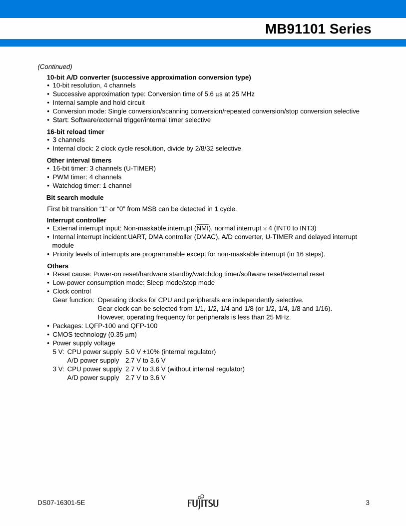


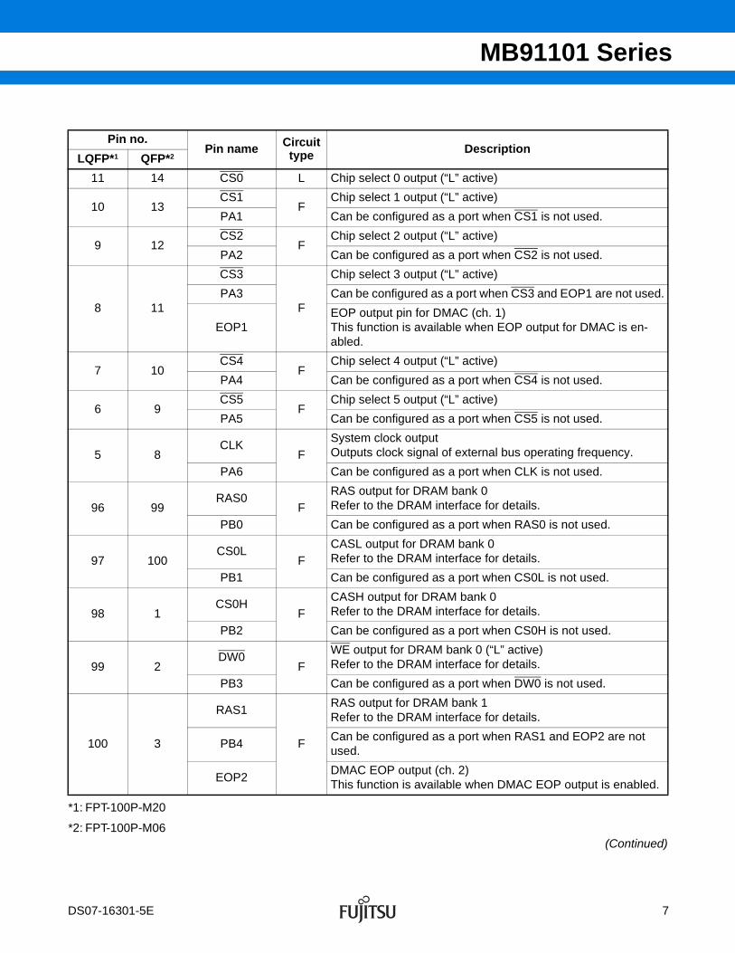


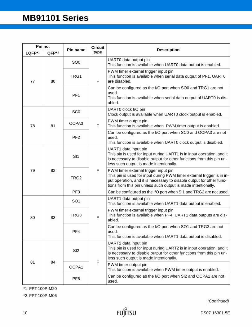

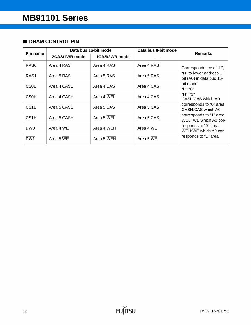
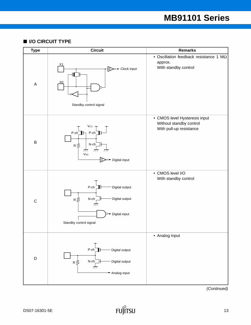
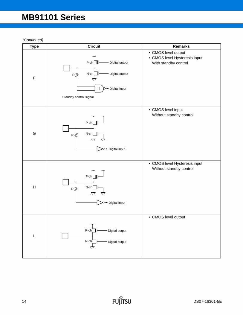
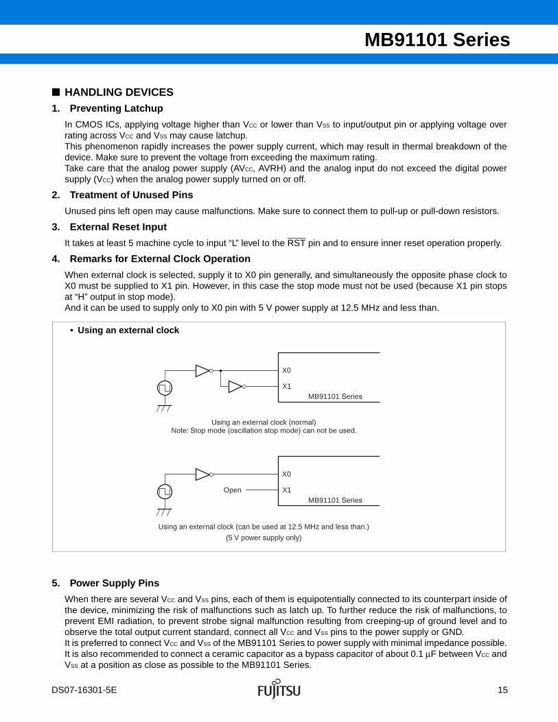


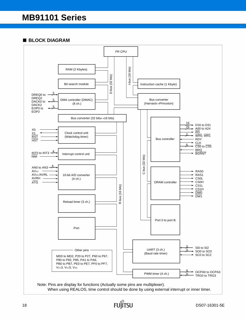


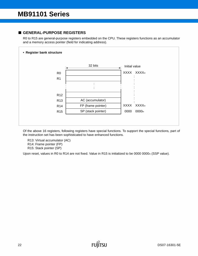


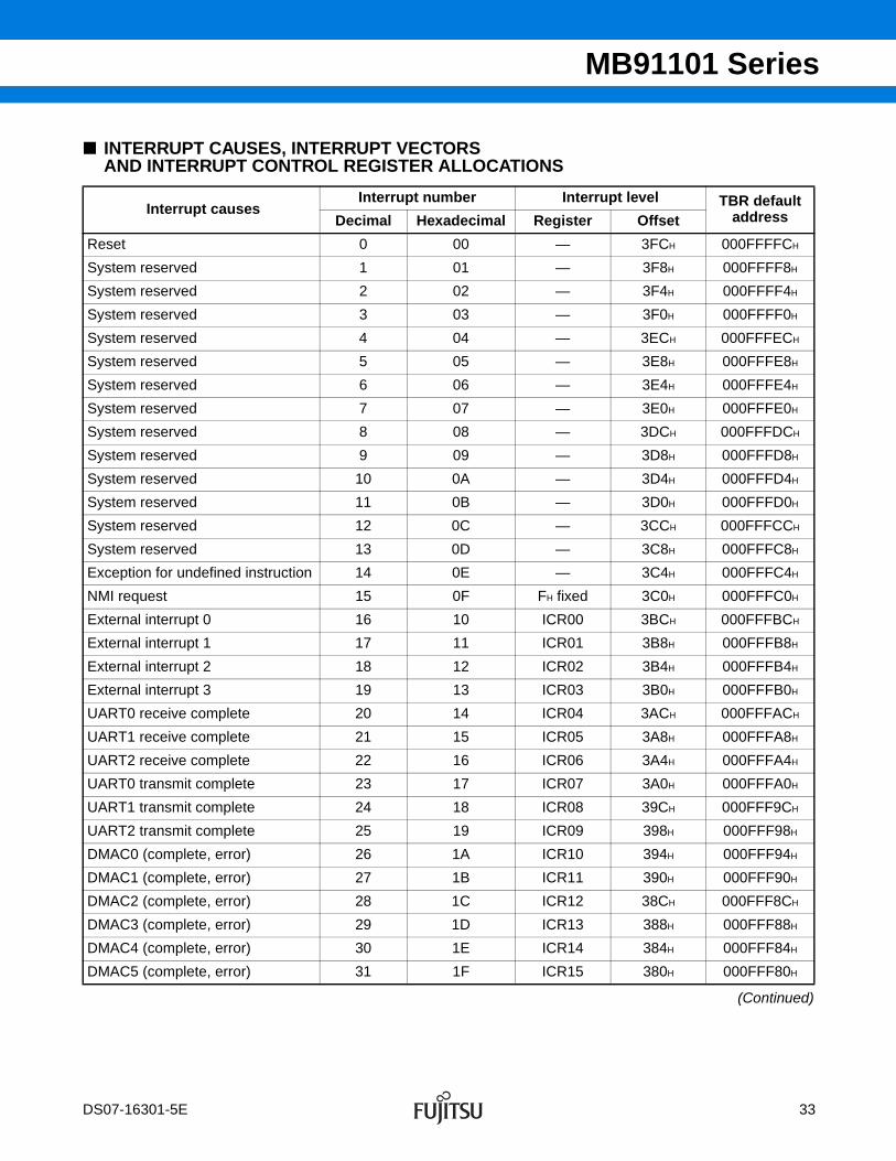


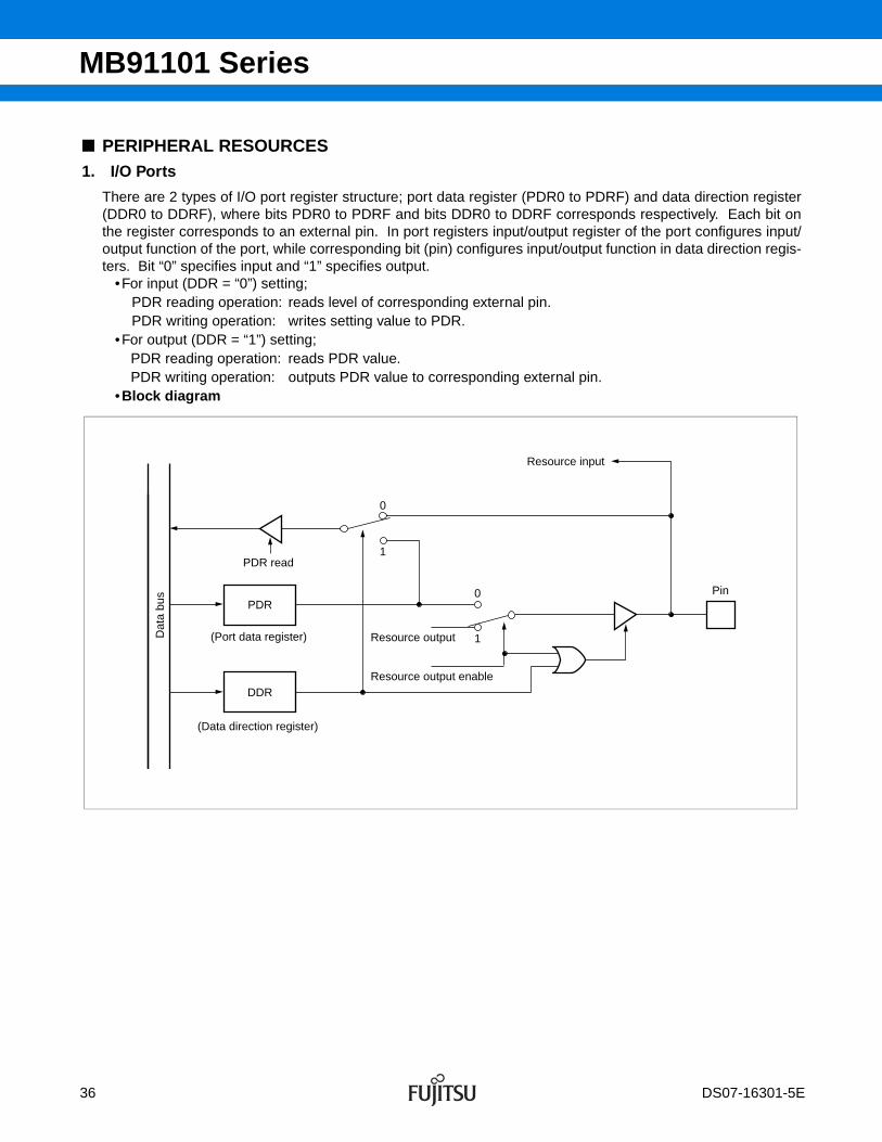


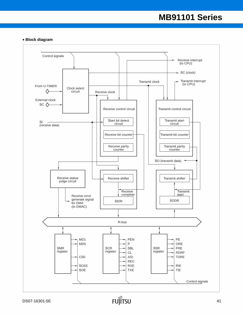

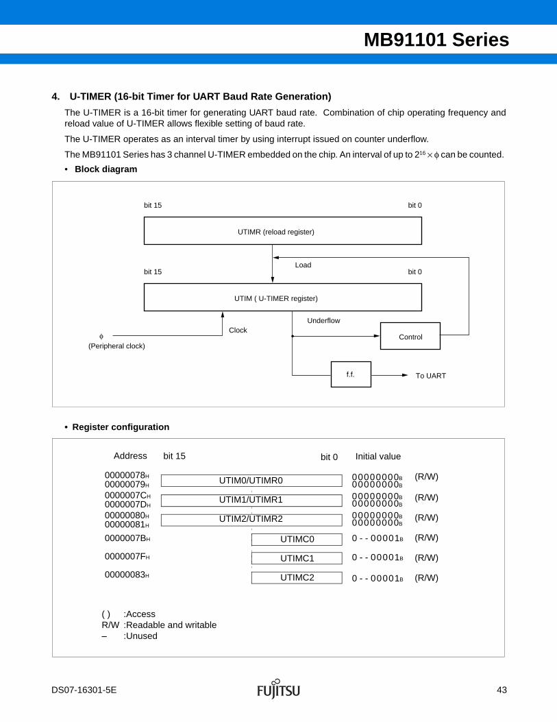


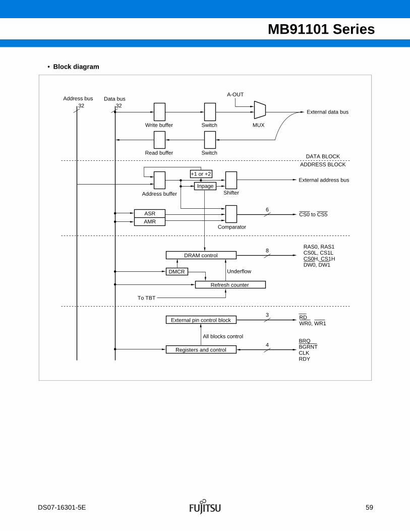


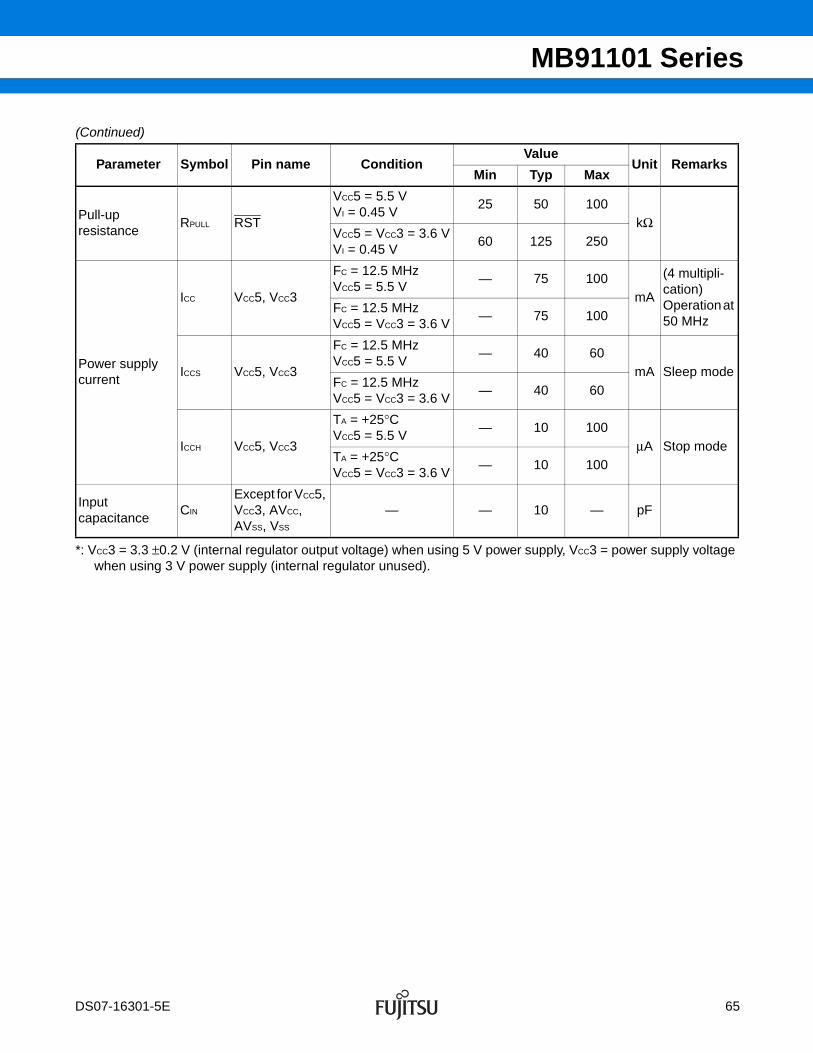
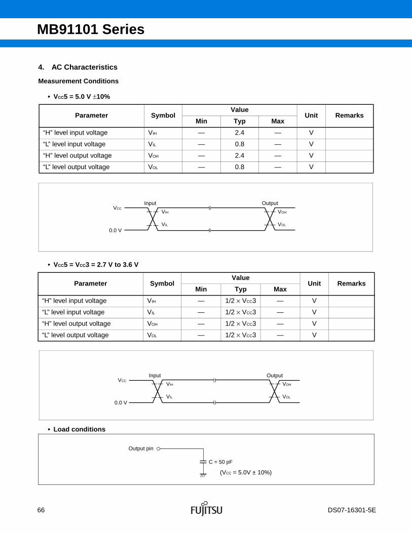

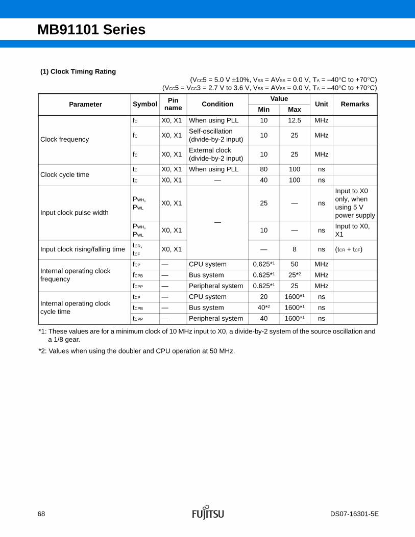


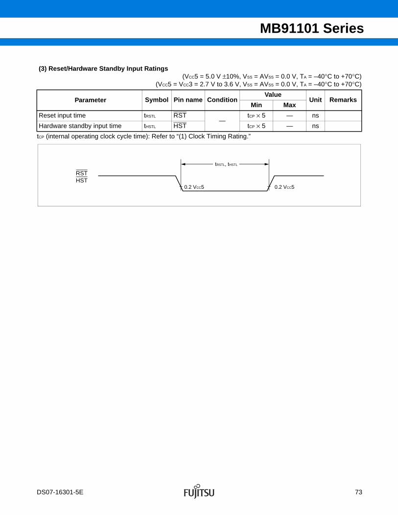

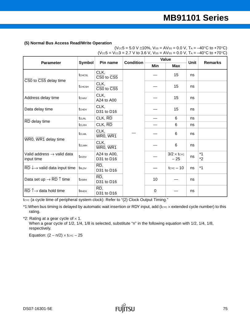


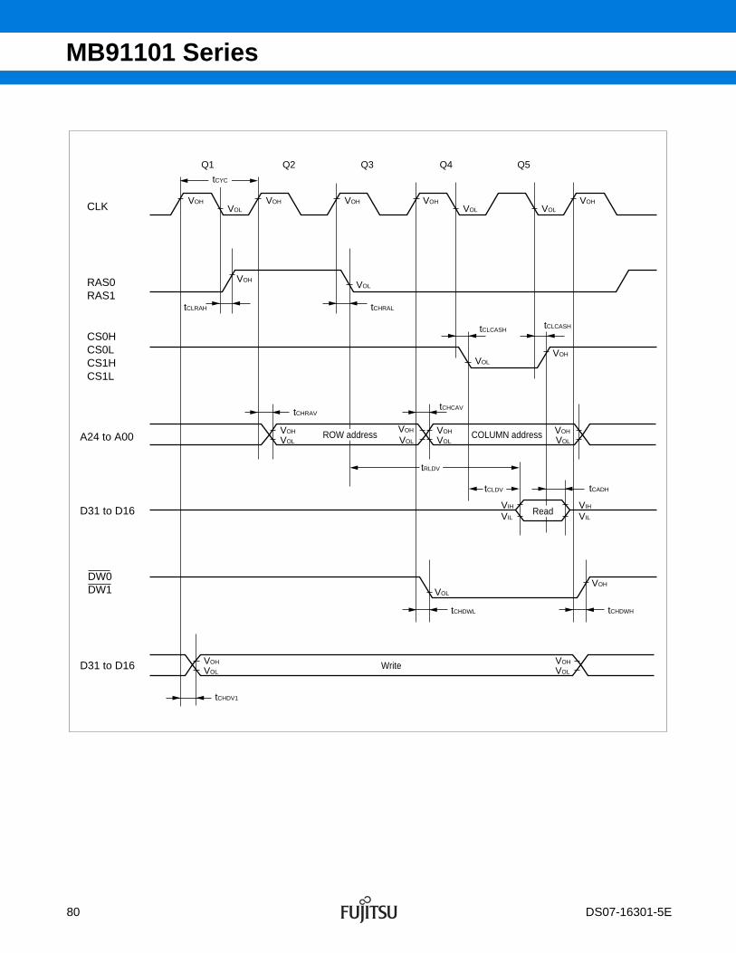

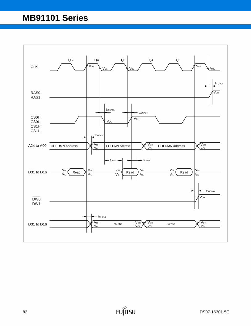
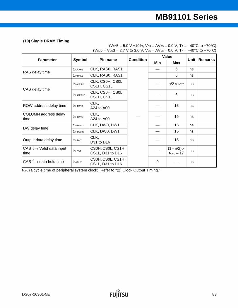


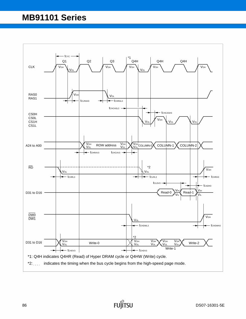
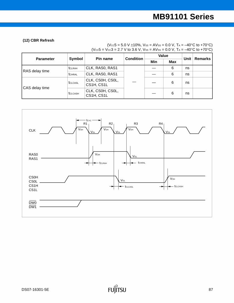


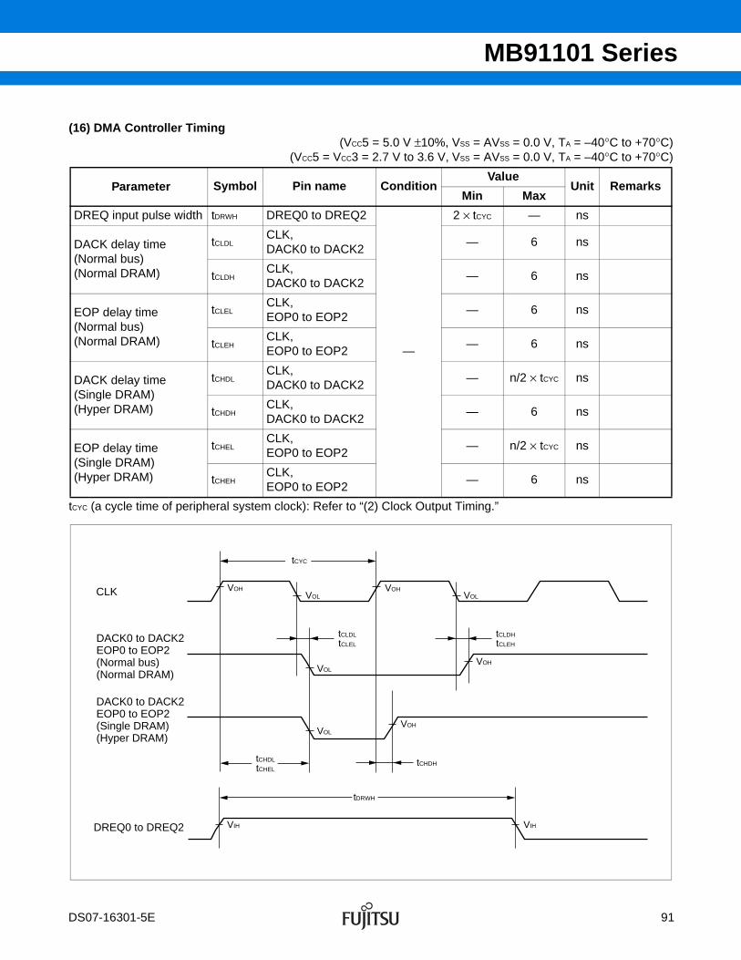


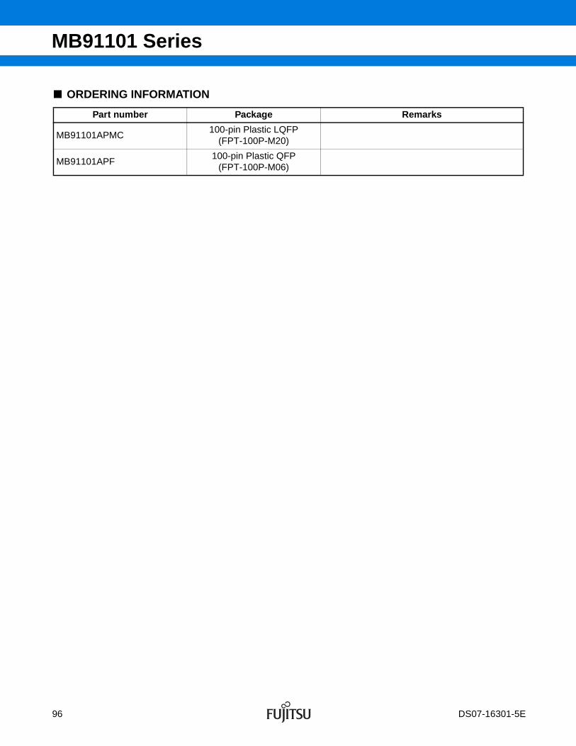
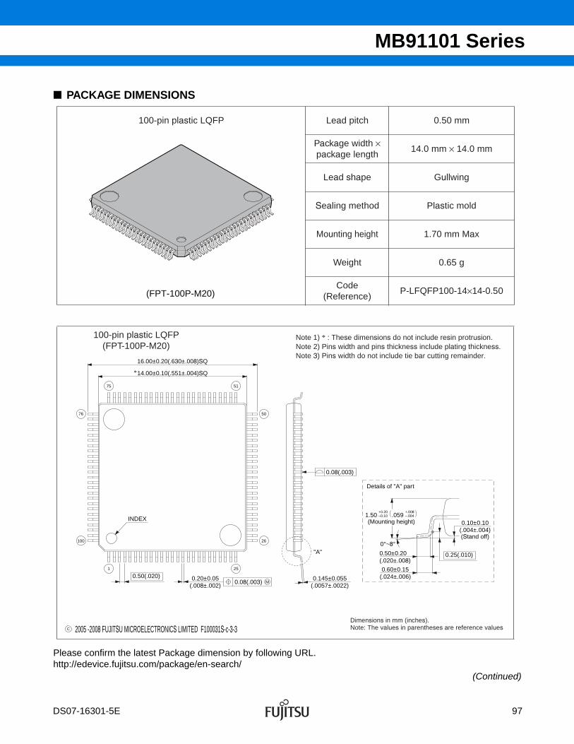
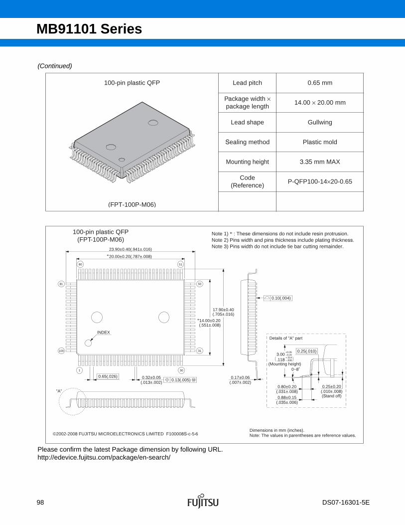


![Atmel AT06475: SAM D21 USB - Microchip Technologyww1.microchip.com/downloads/.../Atmel-42261-SAM-D21... · AT06475: SAM D21 USB [APPLICATION NOTE] 42261A−ARM−03/2014 4 Figure](https://static.documents.pub/doc/80x56/5eb8bb248958705a235105a3/atmel-at06475-sam-d21-usb-microchip-at06475-sam-d21-usb-application-note-42261aaarma032014.jpg)


