9
AN app note FRAM MCU Key Strengths and Applications
AN app note
FRAM MCUKey Strengths and Applications
1
Introduction0 Fujitsu’s Ferroelectric Random Access Memory (FRAM) microcontroller (MCU), which features embedded, non-volatile FRAM, is part of the company’s 8-bit microcontroller 8FX family. The new embedded FRAM memory technology can be configured either as Read-Only Memory (ROM) or Random-Access Memory (RAM). The FRAM microcontroller has the added benefits of high-speed programming and low power consumption.
The FRAM memory technology, its benefits, applications, tools, and software configuration are described below.
FRAM Memory Technology0
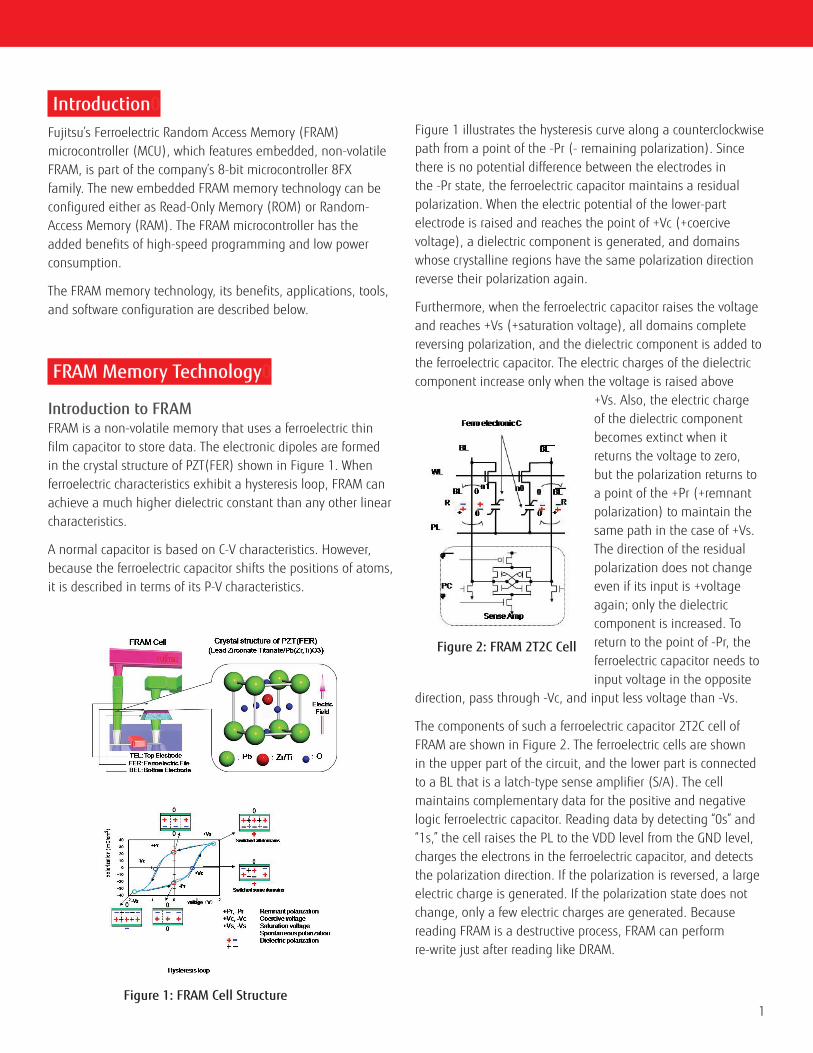
Introduction to FRAMFRAM is a non-volatile memory that uses a ferroelectric thin film capacitor to store data. The electronic dipoles are formed in the crystal structure of PZT(FER) shown in Figure 1. When ferroelectric characteristics exhibit a hysteresis loop, FRAM can achieve a much higher dielectric constant than any other linear characteristics.
A normal capacitor is based on C-V characteristics. However, because the ferroelectric capacitor shifts the positions of atoms, it is described in terms of its P-V characteristics.
Figure 1 illustrates the hysteresis curve along a counterclockwise path from a point of the -Pr (- remaining polarization). Since there is no potential difference between the electrodes in the -Pr state, the ferroelectric capacitor maintains a residual polarization. When the electric potential of the lower-part electrode is raised and reaches the point of +Vc (+coercive voltage), a dielectric component is generated, and domains whose crystalline regions have the same polarization direction reverse their polarization again.
Furthermore, when the ferroelectric capacitor raises the voltage and reaches +Vs (+saturation voltage), all domains complete reversing polarization, and the dielectric component is added to the ferroelectric capacitor. The electric charges of the dielectric component increase only when the voltage is raised above
+Vs. Also, the electric charge of the dielectric component becomes extinct when it returns the voltage to zero, but the polarization returns to a point of the +Pr (+remnant polarization) to maintain the same path in the case of +Vs. The direction of the residual polarization does not change even if its input is +voltage again; only the dielectric component is increased. To return to the point of -Pr, the ferroelectric capacitor needs to input voltage in the opposite
direction, pass through -Vc, and input less voltage than -Vs.
The components of such a ferroelectric capacitor 2T2C cell of FRAM are shown in Figure 2. The ferroelectric cells are shown in the upper part of the circuit, and the lower part is connected to a BL that is a latch-type sense amplifier (S/A). The cell maintains complementary data for the positive and negative logic ferroelectric capacitor. Reading data by detecting “0s” and “1s,” the cell raises the PL to the VDD level from the GND level, charges the electrons in the ferroelectric capacitor, and detects the polarization direction. If the polarization is reversed, a large electric charge is generated. If the polarization state does not change, only a few electric charges are generated. Because reading FRAM is a destructive process, FRAM can perform re-write just after reading like DRAM.
Figure 1: FRAM Cell Structure
Figure 2: FRAM 2T2C Cell
2
FRAM Advantages
Low Power Consumption
FRAM has many advantages compared with other non-volatile memories such as EEPROM. The key advantage of FRAM is its power consumption during the write/erase cycle. Other non-volatile memory requires high voltage to charge or remove electrons in the floating gate, which defines the data as “0” and “1.” The memory has to generate a high voltage, using a charge pump inside the device.
FRAM does not require high voltage to write data; it can operate with normal voltage. Therefore FRAM consumes less power, improving the writing speed.
Figure 3 compares the power consumption of EEPROM and FRAM.
Fast Writing SpeedFRAM can write data much faster than other non-volatile memory primarily because of two factors.
FRAM does not need to erase the data before writing. Before erasing data, other non-volatile memory technologies go through a pre-programming stage to make each floating
gate state stable enough to pull the electrons off the floating gate. Normally memory takes two steps before writing, which takes longer.
Also, FRAM does not need high voltage to write data. Other non-volatile memory technologies require high voltage for erasing. They need on-chip charge pumps to reach a high enough voltage level to proceed with the erasing process. Again, this is time-consuming and wastes power.
Mainly for these two reasons, FRAM can write up to 42,500 times faster than EEPROM as illustrated in Figure 4.
Dynamic Memory SpaceNOR Flash memory is divided into erase blocks or sectors. The erase operation can only be performed on a block or sector basis. This limits how the user can use the memory space. However, FRAM can perform write operations on a bit basis, so the user can set the memory space dynamically, increasing flexibility. This results in a more efficient use of memory space.
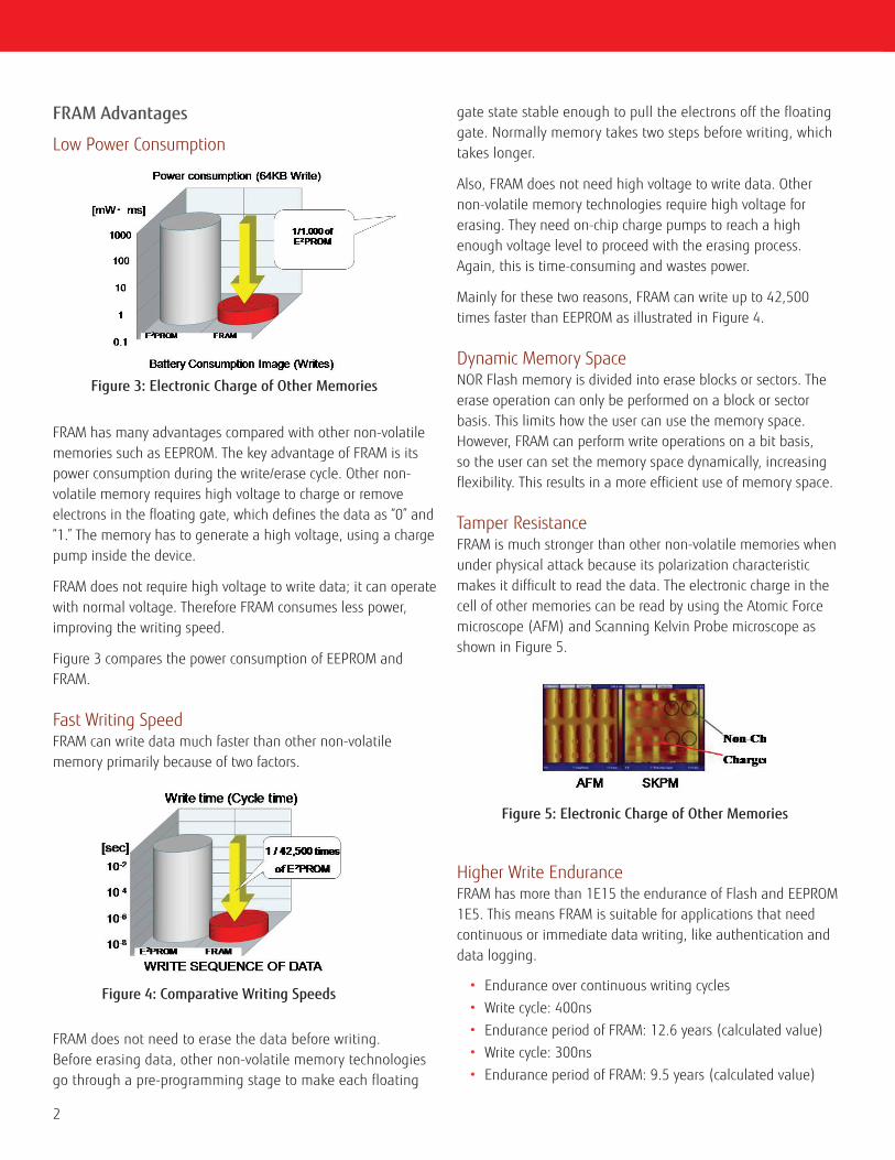
Tamper ResistanceFRAM is much stronger than other non-volatile memories when under physical attack because its polarization characteristic makes it difficult to read the data. The electronic charge in the cell of other memories can be read by using the Atomic Force microscope (AFM) and Scanning Kelvin Probe microscope as shown in Figure 5.
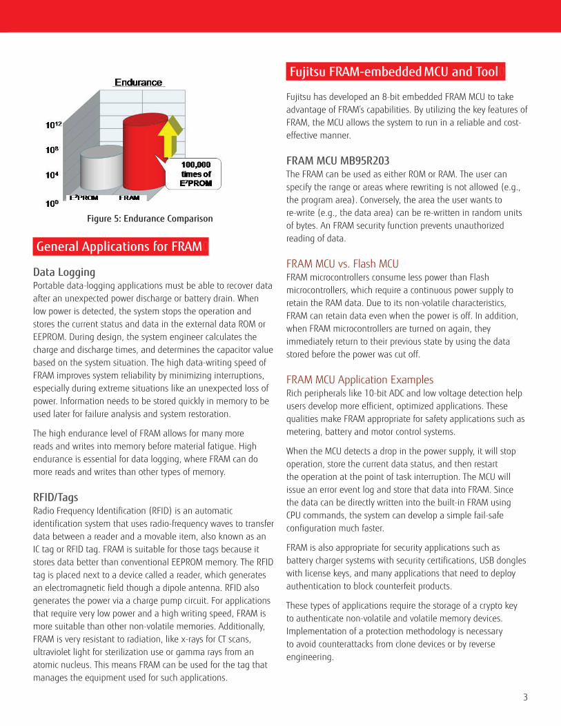
Higher Write EnduranceFRAM has more than 1E15 the endurance of Flash and EEPROM 1E5. This means FRAM is suitable for applications that need continuous or immediate data writing, like authentication and data logging.
Endurance over continuous writing cycles •
Write cycle: 400ns•
Endurance period of FRAM: 12.6 years (calculated value)•
Write cycle: 300ns•
Endurance period of FRAM: 9.5 years (calculated value) •
Figure 5: Electronic Charge of Other Memories
Figure 3: Electronic Charge of Other Memories
Figure 4: Comparative Writing Speeds
3
General Applications for FRAM0
Data LoggingPortable data-logging applications must be able to recover data after an unexpected power discharge or battery drain. When low power is detected, the system stops the operation and stores the current status and data in the external data ROM or EEPROM. During design, the system engineer calculates the charge and discharge times, and determines the capacitor value based on the system situation. The high data-writing speed of FRAM improves system reliability by minimizing interruptions, especially during extreme situations like an unexpected loss of power. Information needs to be stored quickly in memory to be used later for failure analysis and system restoration.
The high endurance level of FRAM allows for many more reads and writes into memory before material fatigue. High endurance is essential for data logging, where FRAM can do more reads and writes than other types of memory.
RFID/TagsRadio Frequency Identification (RFID) is an automatic identification system that uses radio-frequency waves to transfer data between a reader and a movable item, also known as an IC tag or RFID tag. FRAM is suitable for those tags because it stores data better than conventional EEPROM memory. The RFID tag is placed next to a device called a reader, which generates an electromagnetic field though a dipole antenna. RFID also generates the power via a charge pump circuit. For applications that require very low power and a high writing speed, FRAM is more suitable than other non-volatile memories. Additionally, FRAM is very resistant to radiation, like x-rays for CT scans, ultraviolet light for sterilization use or gamma rays from an atomic nucleus. This means FRAM can be used for the tag that manages the equipment used for such applications.
Fujitsu FRAM-embedded MCU and Tool0
Fujitsu has developed an 8-bit embedded FRAM MCU to take advantage of FRAM’s capabilities. By utilizing the key features of FRAM, the MCU allows the system to run in a reliable and cost-effective manner.
FRAM MCU MB95R203The FRAM can be used as either ROM or RAM. The user can specify the range or areas where rewriting is not allowed (e.g., the program area). Conversely, the area the user wants to re-write (e.g., the data area) can be re-written in random units of bytes. An FRAM security function prevents unauthorized reading of data.
FRAM MCU vs. Flash MCU FRAM microcontrollers consume less power than Flash microcontrollers, which require a continuous power supply to retain the RAM data. Due to its non-volatile characteristics, FRAM can retain data even when the power is off. In addition, when FRAM microcontrollers are turned on again, they immediately return to their previous state by using the data stored before the power was cut off.
FRAM MCU Application Examples Rich peripherals like 10-bit ADC and low voltage detection help users develop more efficient, optimized applications. These qualities make FRAM appropriate for safety applications such as metering, battery and motor control systems.
When the MCU detects a drop in the power supply, it will stop operation, store the current data status, and then restart the operation at the point of task interruption. The MCU will issue an error event log and store that data into FRAM. Since the data can be directly written into the built-in FRAM using CPU commands, the system can develop a simple fail-safe configuration much faster.
FRAM is also appropriate for security applications such as battery charger systems with security certifications, USB dongles with license keys, and many applications that need to deploy authentication to block counterfeit products.
These types of applications require the storage of a crypto key to authenticate non-volatile and volatile memory devices. Implementation of a protection methodology is necessary to avoid counterattacks from clone devices or by reverse engineering.
Figure 5: Endurance Comparison
4
FRAM resists physical attacks better than other memory devices. It does not need to implement another protection methodology by software, which can occupy a large amount of ROM and
require a high-performance CPU to operate appropriately, increasing system costs. The FRAM MCU enables a high-security system while minimizing total system costs.
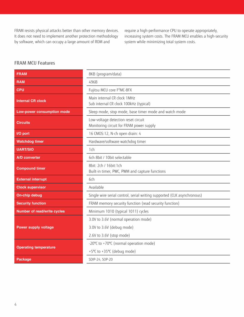
FRAM 8KB (program/data)
RAM 496B
CPU Fujitsu MCU core F²MC-8FX
Internal CR clockMain internal CR clock 1MHzSub internal CR clock 100kHz (typical)
Low-power consumption mode Sleep mode, stop mode, base timer mode and watch mode
CircuitsLow-voltage detection reset circuitMonitoring circuit for FRAM power supply
I/O port 16 CMOS:12, N-ch open drain: 4
Watchdog timer Hardware/software watchdog timer
UART/SIO 1ch
A/D converter 6ch 8bit / 10bit selectable
Compound timer8bit: 2ch / 16bit:1chBuilt-in timer, PWC, PWM and capture functions
External interrupt 6ch
Clock supervisor Available
On-chip debug Single wire serial control, serial writing supported (CLK asynchronous)
Security function FRAM memory security function (read security function)
Number of read/write cycles Minimum 1010 (typical 1011) cycles
Power supply voltage
3.0V to 3.6V (normal operation mode)
3.0V to 3.6V (debug mode)
2.6V to 3.6V (stop mode)
Operating temperature-20ºC to +70ºC (normal operation mode)
+5ºC to +35ºC (debug mode)
Package SDIP-24, SOP-20
FRAM MCU Features
5
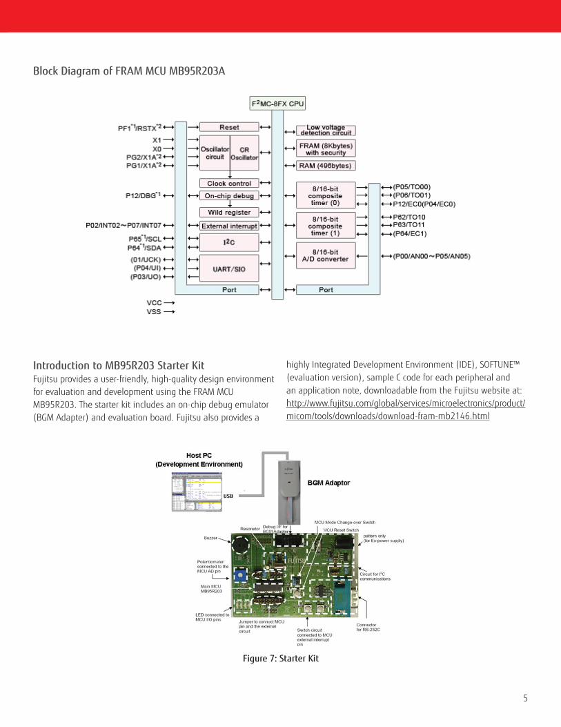
Figure 7: Starter Kit
Block Diagram of FRAM MCU MB95R203A
Introduction to MB95R203 Starter Kit Fujitsu provides a user-friendly, high-quality design environment for evaluation and development using the FRAM MCU MB95R203. The starter kit includes an on-chip debug emulator (BGM Adapter) and evaluation board. Fujitsu also provides a
highly Integrated Development Environment (IDE), SOFTUNE™ (evaluation version), sample C code for each peripheral and an application note, downloadable from the Fujitsu website at: http://www.fujitsu.com/global/services/microelectronics/product/micom/tools/downloads/download-fram-mb2146.html
6
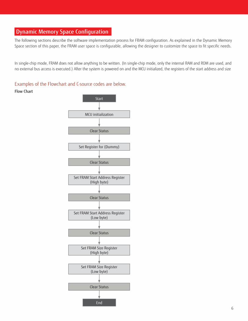
Dynamic Memory Space Configuration0The following sections describe the software implementation process for FRAM configuration. As explained in the Dynamic Memory Space section of this paper, the FRAM user space is configurable, allowing the designer to customize the space to fit specific needs.
In single-chip mode, FRAM does not allow anything to be written. (In single-chip mode, only the internal RAM and ROM are used, and no external bus access is executed.) After the system is powered on and the MCU initialized, the registers of the start address and size
Examples of the Flowchart and C-source codes are below. Flow Chart
MCU initialization
Clear Status
Set Register for (Dummy)
Clear Status
Set FRAM Start Address Register (High byte)
Clear Status
Set FRAM Start Address Register (Low byte)
Clear Status
Set FRAM Size Register (High byte)
Set FRAM Size Register (Low byte)
Start
End
Clear Status
7
Software Example
typedef union{ unsigned short word; struct { unsigned char H; unsigned char L; } byte; } WB;
extern WB FRAM_WE_sadd;extern WB FRAM_WE_size;
FRAM_WRITE(WB FRAM_WE_sadd, WB FRAM_WE_size){ __DI();
IO_FSCR.byte = 0x0C; /* flag clear */
IO_FRAC = 0x00; IO_FRAC = 0x41; IO_FRAC = 0x73; IO_FRAC = 0x68; IO_FAS.byte.FASH = 0x00; /* Dummy address not to set AREA flag */
IO_FSCR.byte = 0x0C; /* flag clear */
IO_FRAC = 0x00; IO_FRAC = 0x41; IO_FRAC = 0x73; IO_FRAC = 0x6C; IO_FAS.byte.FASL = 0x00; /* Dummy address not to set AREA flag */
IO_FSCR.byte = 0x0C; /* flag clear */
IO_FRAC = 0x00; IO_FRAC = 0x61; IO_FRAC = 0x42; IO_FRAC = 0x48; IO_FAB.byte.FABH = FRAM_WE_sadd.byte.H;
IO_FSCR.byte = 0x0C; /* flag clear */
IO_FRAC = 0x00; IO_FRAC = 0x61; IO_FRAC = 0x42; IO_FRAC = 0x4C; IO_FAB.byte.FABL = FRAM_WE_sadd.byte.L; IO_FSCR.byte = 0x0C; /* flag clear */
IO_FRAC = 0x00; IO_FRAC = 0x41; IO_FRAC = 0x73; IO_FRAC = 0x68; IO_FAS.byte.FASH = FRAM_WE_size.byte.H;
IO_FSCR.byte = 0x0C; /* flag clear */
IO_FRAC = 0x00; IO_FRAC = 0x41; IO_FRAC = 0x73; IO_FRAC = 0x6C; IO_FAS.byte.FASL = FRAM_WE_size.byte.L;
IO_FSCR.byte = 0x0C; /* flag clear */
__EI();
8
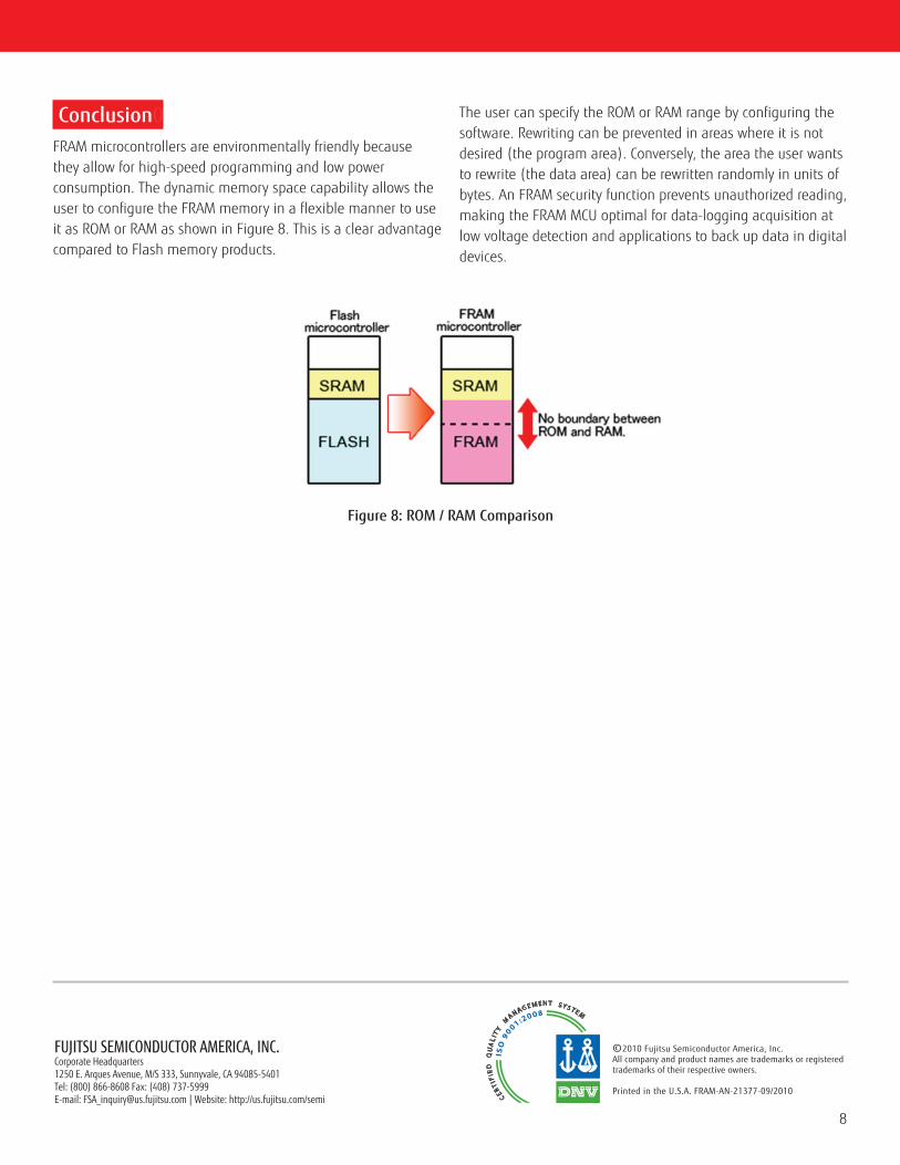
Figure 8: ROM / RAM Comparison
FUjITSU SEMICONDUCTOR AMERICA, INC.Corporate Headquarters1250 E. Arques Avenue, M/S 333, Sunnyvale, CA 94085-5401Tel: (800) 866-8608 Fax: (408) 737-5999E-mail: [email protected] | Website: http://us.fujitsu.com/semi
8
©2010 Fujitsu Semiconductor America, Inc.All company and product names are trademarks or registered trademarks of their respective owners.
Printed in the U.S.A. FRAM-AN-21377-09/2010
Conclusion0FRAM microcontrollers are environmentally friendly because they allow for high-speed programming and low power consumption. The dynamic memory space capability allows the user to configure the FRAM memory in a flexible manner to use it as ROM or RAM as shown in Figure 8. This is a clear advantage compared to Flash memory products.
The user can specify the ROM or RAM range by configuring the software. Rewriting can be prevented in areas where it is not desired (the program area). Conversely, the area the user wants to rewrite (the data area) can be rewritten randomly in units of bytes. An FRAM security function prevents unauthorized reading, making the FRAM MCU optimal for data-logging acquisition at low voltage detection and applications to back up data in digital devices.


