This document contains information on a product under development. Freescale reserves the right to change or discontinue this product without notice.
MPC5604B/C
TBD
MAPBGA–22515 mm x 15 mm
QFN12##_mm_x_##mm
SOT-343R##_mm_x_##mm
PKG-TBD## mm x ## mm
208 MAPBGA(17 x 17 x 1.7 mm)
144 LQFP(20 x 20 x 1.4 mm)
100 LQFP(14 x 14 x 1.4 mm)
64 LQFP(10 x 10 x 1.4 mm)
Features
• Single issue, 32-bit CPU core complex (e200z0)
— Compliant with the Power Architecture® embedded category
— Includes an instruction set enhancement allowing variable length encoding (VLE) for code size footprint reduction. With the optional encoding of mixed 16-bit and 32-bit instructions, it is possible to achieve significant code size footprint reduction.
• Up to 512 KB on-chip code flash supported with the flash controller and ECC
• 64 (4 × 16) KB on-chip data flash memory with ECC
• Up to 48 KB on-chip SRAM with ECC
• Memory protection unit (MPU) with 8 region descriptors and 32-byte region granularity
• Interrupt controller (INTC) with 148 interrupt vectors, including 16 external interrupt sources and 18 external interrupt/wakeup sources
• Frequency modulated phase-locked loop (FMPLL)
• Crossbar switch architecture for concurrent access to peripherals, flash memory, or RAM from multiple bus masters
• Boot assist module (BAM) supports internal flash programming via a serial link (CAN or SCI)
• Timer supports input/output channels providing a range of 16-bit input capture, output compare, and pulse width modulation functions (eMIOS-lite)
• 10-bit analog-to-digital converter (ADC)
• 3 serial peripheral interface (DSPI) modules
• Up to 4 serial communication interface (LINFlex) modules
MPC5604B/CMicrocontroller Data Sheet
• Up to 6 enhanced full CAN (FlexCAN) modules with configurable buffers
• 1 inter IC communication interface (I2C) module
• Up to 123 configurable general purpose pins supporting input and output operations (package dependent)
• Real Time Counter (RTC) with clock source from 128 kHz or 16 MHz internal RC oscillator supporting autonomous wakeup with 1 ms resolution with max timeout of 2 seconds
• Up to 6 periodic interrupt timers (PIT) with 32-bit counter resolution
• 1 System Module Timer (STM)
• Nexus development interface (NDI) per IEEE-ISTO 5001-2003 Class Two Plus standard
• Device/board boundary Scan testing supported with per Joint Test Action Group (JTAG) of IEEE (IEEE 1149.1)
• On-chip voltage regulator (VREG) for regulation of input supply for all internal levels
1.1 Document overviewThis document describes the features of the family and options available within the family members, and highlights important electrical and physical characteristics of the device. To ensure a complete understanding of the device functionality, refer also to the device reference manual and errata sheet.
1.2 DescriptionThe MPC5604B/C is a family of next generation microcontrollers built on the Power Architecture® embedded category.
The MPC5604B/C family of 32-bit microcontrollers is the latest achievement in integrated automotive application controllers. It belongs to an expanding family of automotive-focused products designed to address the next wave of body electronics applications within the vehicle. The advanced and cost-efficient host processor core of this automotive controller family complies with the Power Architecture embedded category and only implements the VLE (variable-length encoding) APU, providing improved code density. It operates at speeds of up to 64 MHz and offers high performance processing optimized for low power consumption. It capitalizes on the available development infrastructure of current Power Architecture devices and is supported with software drivers, operating systems and configuration code to assist with users implementations.
1 Feature set dependent on selected peripheral multiplexing—table shows example implementation.2 Based on 125 °C ambient operating temperature.3 See the eMIOS section of the device reference manual for information on the channel configuration and functions.4 IC – Input Capture; OC – Output Compare; PWM – Pulse Width Modulation; MC – Modulus counter.5 SCI0, SCI1 and SCI2 are available. SCI3 is not available.6 CAN0, CAN1 are available. CAN2, CAN3, CAN4 and CAN5 are not available.7 CAN0, CAN3 and either CAN1 or CAN4 are available. CAN2, CAN5 and CAN6 are not available8 I/O count based on multiplexing with peripherals.9 208 MAPBGA available only as development package for Nexus2+.
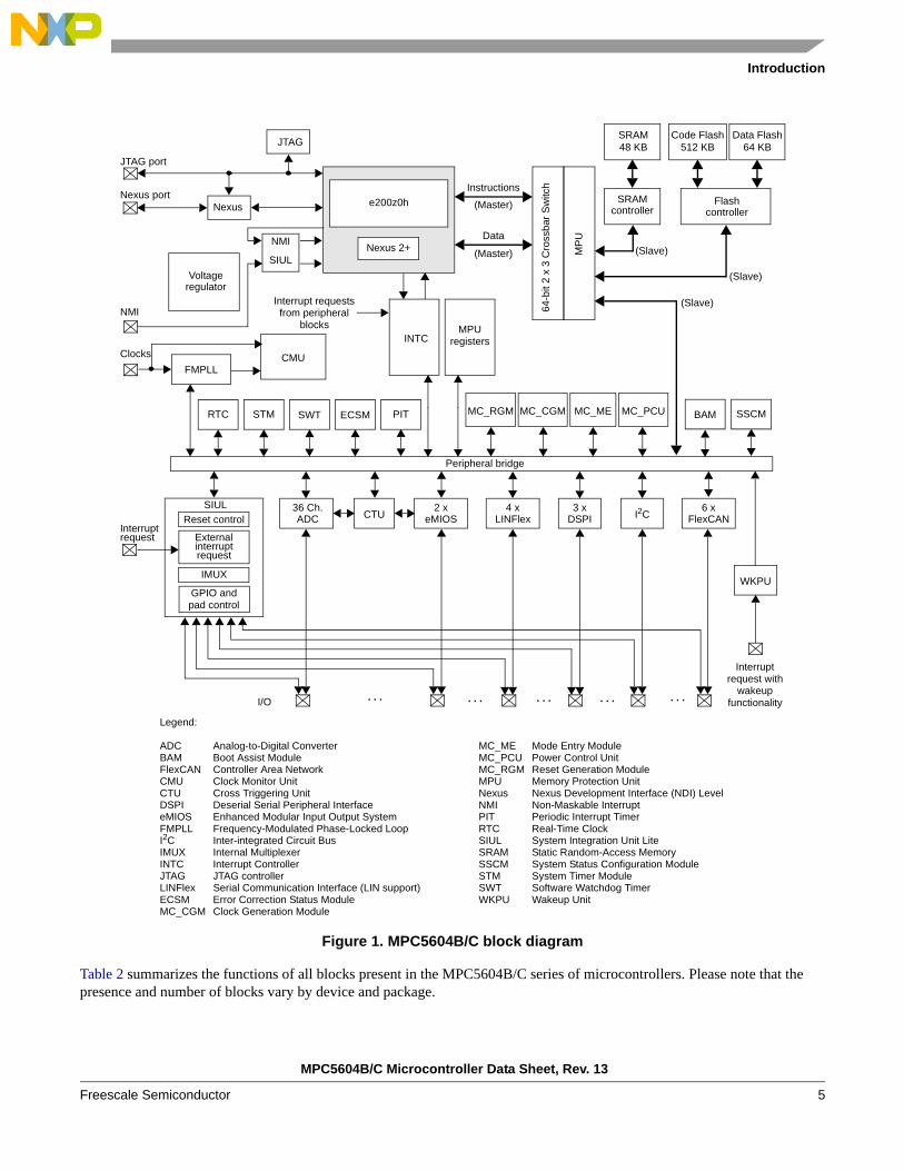
Table 2 summarizes the functions of all blocks present in the MPC5604B/C series of microcontrollers. Please note that the presence and number of blocks vary by device and package.
3 xDSPI
FMPLL
Nexus 2+
Nexus
SRAM
SIUL
Reset control
48 KB
External
IMUX
GPIO and
JTAG
pad control
JTAG port
Nexus porte200z0h
Interrupt requests
64-b
it 2
x 3
Cro
ssb
ar
Sw
itch
6 xFlexCAN
Peripheral bridge
interruptrequest
Interruptrequest
I/O
Clocks
Instructions
Data
Voltageregulator
NMI
SWT PITSTM
NMI
SIUL
. . . . . . . . .. . .
INTC
I2C
. . .
4 xLINFlex
2 xeMIOS
36 Ch.ADC
MP
U
CMU
SRAM Flash
Code Flash512 KB
Data Flash64 KB
MC_PCUMC_MEMC_CGMMC_RGM BAM
CTU
RTC SSCM
(Master)
(Master)
(Slave)
(Slave)
(Slave)
controllercontroller
Legend:
ADC Analog-to-Digital ConverterBAM Boot Assist ModuleFlexCAN Controller Area NetworkCMU Clock Monitor UnitCTU Cross Triggering UnitDSPI Deserial Serial Peripheral InterfaceeMIOS Enhanced Modular Input Output SystemFMPLL Frequency-Modulated Phase-Locked LoopI2C Inter-integrated Circuit BusIMUX Internal MultiplexerINTC Interrupt ControllerJTAG JTAG controllerLINFlex Serial Communication Interface (LIN support)ECSM Error Correction Status ModuleMC_CGM Clock Generation Module
MC_ME Mode Entry ModuleMC_PCU Power Control UnitMC_RGM Reset Generation ModuleMPU Memory Protection UnitNexus Nexus Development Interface (NDI) LevelNMI Non-Maskable InterruptPIT Periodic Interrupt TimerRTC Real-Time ClockSIUL System Integration Unit LiteSRAM Static Random-Access MemorySSCM System Status Configuration ModuleSTM System Timer ModuleSWT Software Watchdog TimerWKPU Wakeup Unit
Boot assist module (BAM) A block of read-only memory containing VLE code which is executed according to the boot mode of the device
Clock monitor unit (CMU) Monitors clock source (internal and external) integrity
Cross triggering unit (CTU) Enables synchronization of ADC conversions with a timer event from the eMIOS or from the PIT
Deserial serial peripheral interface (DSPI)
Provides a synchronous serial interface for communication with external devices
Error Correction Status Module (ECSM)
Provides a myriad of miscellaneous control functions for the device including program-visible information about configuration and revision levels, a reset status register, wakeup control for exiting sleep modes, and optional features such as information on memory errors reported by error-correcting codes
Enhanced Direct Memory Access (eDMA)
Performs complex data transfers with minimal intervention from a host processor via “n” programmable channels.
Enhanced modular input output system (eMIOS)
Provides the functionality to generate or measure events
Flash memory Provides non-volatile storage for program code, constants and variables
FlexCAN (controller area network) Supports the standard CAN communications protocol
Frequency-modulated phase-locked loop (FMPLL)
Generates high-speed system clocks and supports programmable frequency modulation
Internal multiplexer (IMUX) SIU subblock
Allows flexible mapping of peripheral interface on the different pins of the device
Inter-integrated circuit (I2C™) bus A two wire bidirectional serial bus that provides a simple and efficient method of data exchange between devices
Interrupt controller (INTC) Provides priority-based preemptive scheduling of interrupt requests
JTAG controller Provides the means to test chip functionality and connectivity while remaining transparent to system logic when not in test mode
LINFlex controller Manages a high number of LIN (Local Interconnect Network protocol) messages efficiently with a minimum of CPU load
Clock generation module (MC_CGM)
Provides logic and control required for the generation of system and peripheral clocks
Mode entry module (MC_ME) Provides a mechanism for controlling the device operational mode and mode transition sequences in all functional states; also manages the power control unit, reset generation module and clock generation module, and holds the configuration, control and status registers accessible for applications
Power control unit (MC_PCU) Reduces the overall power consumption by disconnecting parts of the device from the power supply via a power switching device; device components are grouped into sections called “power domains” which are controlled by the PCU
Reset generation module (MC_RGM)
Centralizes reset sources and manages the device reset sequence of the device
Memory protection unit (MPU) Provides hardware access control for all memory references generated in a device
Package pinouts and signal descriptions
MPC5604B/C Microcontroller Data Sheet, Rev. 13
Freescale Semiconductor 7
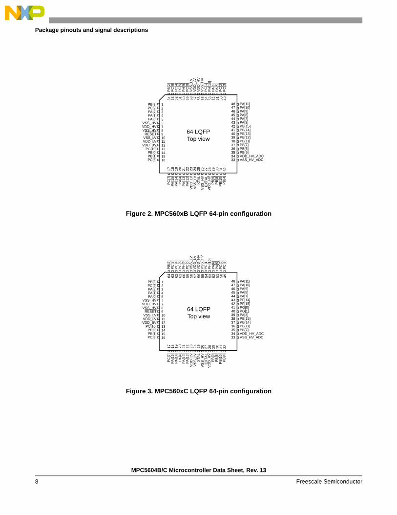
2 Package pinouts and signal descriptions
2.1 Package pinoutsThe available LQFP pinouts and the 208 MAPBGA ballmap are provided in the following figures. For pin signal descriptions, please refer to the device reference manual.
Nexus development interface (NDI)
Provides real-time development support capabilities in compliance with the IEEE-ISTO 5001-2003 standard
Periodic interrupt timer (PIT) Produces periodic interrupts and triggers
Real-time counter (RTC) A free running counter used for time keeping applications, the RTC can be configured to generate an interrupt at a predefined interval independent of the mode of operation (run mode or low-power mode)
System integration unit (SIU) Provides control over all the electrical pad controls and up 32 ports with 16 bits of bidirectional, general-purpose input and output signals and supports up to 32 external interrupts with trigger event configuration
Static random-access memory (SRAM)
Provides storage for program code, constants, and variables
System status configuration module (SSCM)
Provides system configuration and status data (such as memory size and status, device mode and security status), device identification data, debug status port enable and selection, and bus and peripheral abort enable/disable
System timer module (STM) Provides a set of output compare events to support AUTOSAR (Automotive Open System Architecture) and operating system tasks
Software watchdog timer (SWT) Provides protection from runaway code
Wakeup unit (WKPU) The wakeup unit supports up to 18 external sources that can generate interrupts or wakeup events, of which 1 can cause non-maskable interrupt requests or wakeup events.
Crossbar (XBAR) switch Supports simultaneous connections between two master ports and three slave ports. The crossbar supports a 32-bit address bus width and a 64-bit data bus width.
Table 2. MPC5604B/C series block summary (continued)
R PF[12] PC[6] PF[10] PF[11] VDD_HV PA[15] PA[13] NCOSC32K_XTAL
PF[3] PF[7] PD[2] PD[4] PD[7]VSS_HV
_ADCPB[5] R
T NC NC NC MCKO NC PF[13] PA[12] NCOSC32K_EXTAL
PF[2] PF[6] PD[1] PD[5] PD[6] PD[8] PB[4] T
1 2 3 4 5 6 7 8 9 10 11 12 13 14 15 16
Note: 208 MAPBGA available only as development package for Nexus 2+. NC = Not connected
Figure 6. 208 MAPBGA configuration
MPC5604B/C Microcontroller Data Sheet, Rev. 13
Package pinouts and signal descriptions
Freescale Semiconductor12
• Nexus output pads (MDO[n], MCKO, EVTO, MSEO) are forced to output.
2.3 Voltage supply pinsVoltage supply pins are used to provide power to the device. Three dedicated VDD_LV/VSS_LV supply pairs are used for 1.2 V regulator stabilization.
2.4 Pad typesIn the device the following types of pads are available for system pins and functional port pins:
S = Slow1
M = Medium1 2
F = Fast1 2
I = Input only with analog feature1
J = Input/Output (‘S’ pad) with analog feature
X = Oscillator
Table 3. Voltage supply pin descriptions
Port pin FunctionPin number
64 LQFP1
1 Pin numbers apply to both the MPC560xB and MPC560xC packages.
100 LQFP 144 LQFP 208 MAPBGA2
2 208 MAPBGA available only as development package for Nexus2+
VDD_HV Digital supply voltage 7, 28, 56 15, 37, 70, 84 19, 51, 100, 123
VDD_LV 1.2V decoupling pins. Decoupling capacitor must be connected between these pins and the nearest VSS_LV pin.3
3 A decoupling capacitor must be placed between each of the three VDD_LV/VSS_LV supply pairs to ensure stable voltage (see the recommended operating conditions in the device datasheet for details).
11, 23, 57 19, 32, 85 23, 46, 124 D8, K4, P7
VSS_LV 1.2V decoupling pins. Decoupling capacitor must be connected between these pins and the nearest VDD_LV pin.3
10, 24, 58 18, 33, 86 22, 47, 125 C8, J2, N7
VDD_BV Internal regulator supply voltage 12 20 24 K3
VSS_HV_ADC Reference ground and analog ground for the ADC
33 51 73 R15
VDD_HV_ADC Reference voltage and analog supply for the ADC
34 52 74 P14
1. See the I/O pad electrical characteristics in the device datasheet for details.2. All medium and fast pads are in slow configuration by default at reset and can be configured as fast or medium (see PCR.SRC in section Pad Configuration Registers (PCR0–PCR122) in the device reference manual).
Package pinouts and signal descriptions
MPC5604B/C Microcontroller Data Sheet, Rev. 13
Freescale Semiconductor 13
2.5 System pinsThe system pins are listed in Table 4.
2.6 Functional portsThe functional port pins are listed in Table 5.
Table 4. System pin descriptions
Sy
stem
pin
Function
I/O d
irec
tio
n
Pad
typ
e
RE
SE
T c
on
fig
ura
tio
n Pin number
64L
QF
P1
1 Pin numbers apply to both the MPC560xB and MPC560xC packages.
100
LQ
FP
144
LQ
FP
208
MA
PB
GA
2
2 208 MAPBGA available only as development package for Nexus2+
RESET Bidirectional reset with Schmitt-Trigger characteristics and noise filter.
I/O M Input, weak pull-up only
after PHASE2
9 17 21 J1
EXTAL Analog output of the oscillator amplifier circuit, when the oscillator is not in bypass mode.Analog input for the clock generator when the oscillator is in bypass mode.3
3 See the relevant section of the datasheet
I/O X Tristate 27 36 50 N8
XTAL Analog input of the oscillator amplifier circuit. Needs to be grounded if oscillator is used in bypass mode.3
I X Tristate 25 34 48 P8
Table 5. Functional port pin descriptions
Po
rt p
in
PC
R
Alt
ern
ate
fun
ctio
n1
Fu
nc
tio
n
Per
iph
eral
I/O d
irec
tio
n2
Pad
typ
e
RE
SE
T c
on
fig
ura
tio
n Pin number
MP
C56
0xB
64
LQ
FP
MP
C56
0xC
64
LQ
FP
100
LQ
FP
144
LQ
FP
208
MA
PB
GA
3
PA[0] PCR[0] AF0AF1AF2AF3—
GPIO[0]E0UC[0]CLKOUT
—WKPU[19]4
SIULeMIOS_0
CGL—
WKPU
I/OI/OO—I
M Tristate 5 5 12 16 G4
PA[1] PCR[1] AF0AF1AF2AF3——
GPIO[1]E0UC[1]
——
NMI5
WKPU[2]4
SIULeMIOS_0
——
WKPUWKPU
I/OI/O——II
S Tristate 4 4 7 11 F3
MPC5604B/C Microcontroller Data Sheet, Rev. 13
Package pinouts and signal descriptions
Freescale Semiconductor14
PA[2] PCR[2] AF0AF1AF2AF3—
GPIO[2]E0UC[2]
——
WKPU[3]4
SIULeMIOS_0
——
WKPU
I/OI/O——I
S Tristate 3 3 5 9 F2
PA[3] PCR[3] AF0AF1AF2AF3—
GPIO[3]E0UC[3]
——
EIRQ[0]
SIULeMIOS_0
——
SIUL
I/OI/O——I
S Tristate 43 39 68 90 K15
PA[4] PCR[4] AF0AF1AF2AF3—
GPIO[4]E0UC[4]
——
WKPU[9]4
SIULeMIOS_0
——
WKPU
I/OI/O——I
S Tristate 20 20 29 43 N6
PA[5] PCR[5] AF0AF1AF2AF3
GPIO[5]E0UC[5]
——
SIULeMIOS_0
——
I/OI/O——
M Tristate 51 51 79 118 C11
PA[6] PCR[6] AF0AF1AF2AF3—
GPIO[6]E0UC[6]
——
EIRQ[1]
SIULeMIOS_0
——
SIUL
I/OI/O——I
S Tristate 52 52 80 119 D11
PA[7] PCR[7] AF0AF1AF2AF3—
GPIO[7]E0UC[7]LIN3TX
—EIRQ[2]
SIULeMIOS_0LINFlex_3
—SIUL
I/OI/OO—I
S Tristate 44 44 71 104 D16
PA[8] PCR[8] AF0AF1AF2AF3—
N/A6
—
GPIO[8]E0UC[8]
——
EIRQ[3]ABS[0]LIN3RX
SIULeMIOS_0
——
SIULBAM
LINFlex_3
I/OI/O——III
S Input, weakpull-up
45 45 72 105 C16
PA[9] PCR[9] AF0AF1AF2AF3N/A6
GPIO[9]E0UC[9]
——
FAB
SIULeMIOS_0
——
BAM
I/OI/O——I
S Pull-down 46 46 73 106 C15
Table 5. Functional port pin descriptions (continued)
Po
rt p
in
PC
R
Alt
ern
ate
fun
ctio
n1
Fu
nct
ion
Per
iph
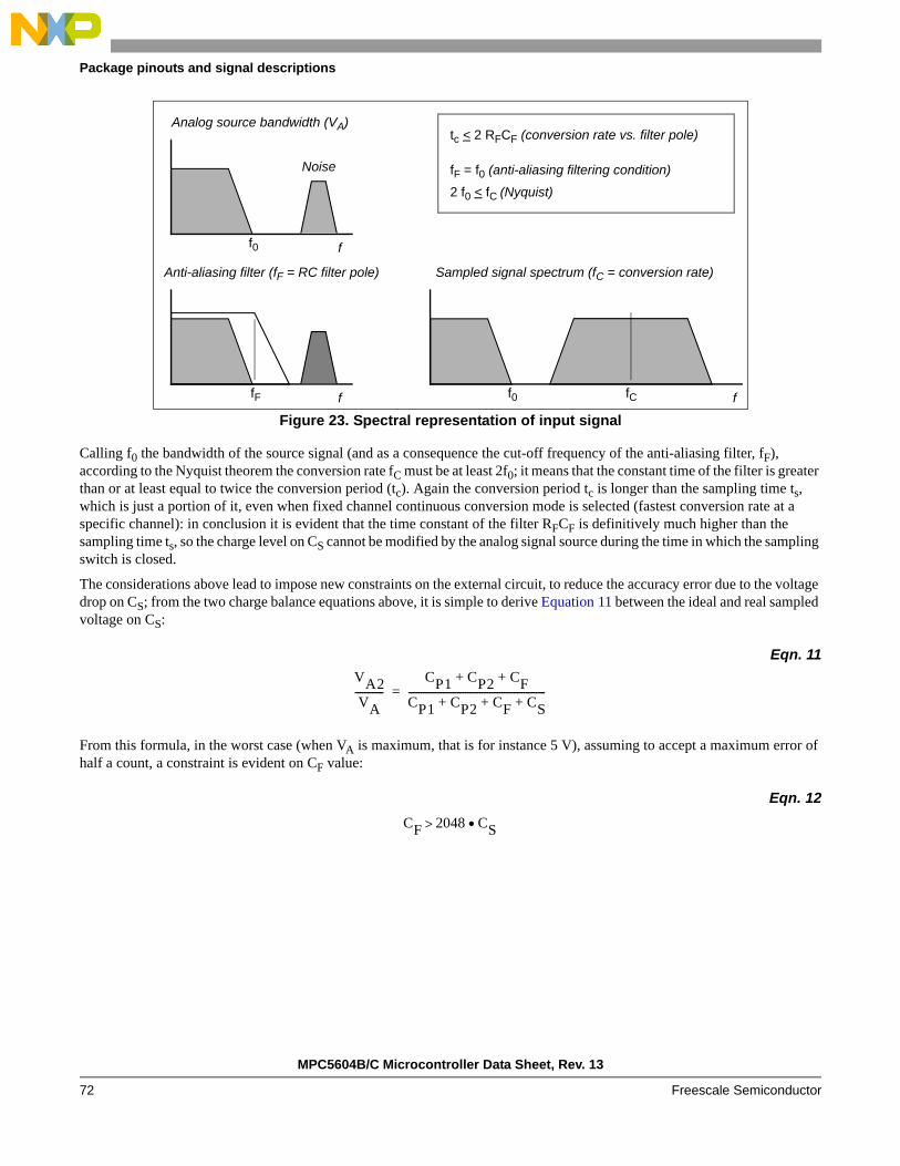
eral
I/O d
irec
tio
n2
Pa
d t
ype
RE
SE
T c
on
fig
ura
tio
n Pin number
MP
C56
0xB
64
LQ
FP
MP
C56
0xC
64
LQ
FP
100
LQ
FP
144
LQ
FP
208
MA
PB
GA
3
Package pinouts and signal descriptions
MPC5604B/C Microcontroller Data Sheet, Rev. 13
Freescale Semiconductor 15
PA[10] PCR[10] AF0AF1AF2AF3
GPIO[10]E0UC[10]
SDA—
SIULeMIOS_0
I2C_0—
I/OI/OI/O—
S Tristate 47 47 74 107 B16
PA[11] PCR[11] AF0AF1AF2AF3
GPIO[11]E0UC[11]
SCL—
SIULeMIOS_0
I2C_0—
I/OI/OI/O—
S Tristate 48 48 75 108 B15
PA[12] PCR[12] AF0AF1AF2AF3—
GPIO[12]———
SIN_0
SIUL———
DSPI0
I/O———I
S Tristate 22 22 31 45 T7
PA[13] PCR[13] AF0AF1AF2AF3
GPIO[13]SOUT_0
——
SIULDSPI_0
——
I/OO——
M Tristate 21 21 30 44 R7
PA[14] PCR[14] AF0AF1AF2AF3—
GPIO[14]SCK_0CS0_0
—EIRQ[4]
SIULDSPI_0DSPI_0
—SIUL
I/OI/OI/O—I
M Tristate 19 19 28 42 P6
PA[15] PCR[15] AF0AF1AF2AF3—
GPIO[15]CS0_0SCK_0
—WKPU[10]4
SIULDSPI_0DSPI_0
—WKPU
I/OI/OI/O—I
M Tristate 18 18 27 40 R6
PB[0] PCR[16] AF0AF1AF2AF3
GPIO[16]CAN0TX
——
SIULFlexCAN_0
——
I/OO——
M Tristate 14 14 23 31 N3
PB[1] PCR[17] AF0AF1AF2AF3——
GPIO[17]———
WKPU[4]4
CAN0RX
SIUL———
WKPUFlexCAN_0
I/O———II
S Tristate 15 15 24 32 N1
PB[2] PCR[18] AF0AF1AF2AF3
GPIO[18]LIN0TX
SDA—
SIULLINFlex_0
I2C_0—
I/OOI/O—
M Tristate 64 64 100 144 B2
Table 5. Functional port pin descriptions (continued)
Po
rt p
in
PC
R
Alt
ern
ate
fun
ctio
n1
Fu
nct
ion
Per
iph
eral
I/O d
irec
tio
n2
Pa
d t
ype
RE
SE
T c
on
fig
ura
tio
n Pin number
MP
C56
0xB
64
LQ
FP
MP
C56
0xC
64
LQ
FP
100
LQ
FP
144
LQ
FP
208
MA
PB
GA
3
MPC5604B/C Microcontroller Data Sheet, Rev. 13
Package pinouts and signal descriptions
Freescale Semiconductor16
PB[3] PCR[19] AF0AF1AF2AF3——
GPIO[19]—
SCL—
WKPU[11]4
LIN0RX
SIUL—
I2C_0—
WKPULINFlex_0
I/O—I/O—II
S Tristate 1 1 1 1 C3
PB[4] PCR[20] AF0AF1AF2AF3—
GPIO[20]———
GPI[0]
SIUL———
ADC
I———I
I Tristate 32 32 50 72 T16
PB[5] PCR[21] AF0AF1AF2AF3—
GPIO[21]———
GPI[1]
SIUL———
ADC
I———I
I Tristate 35 — 53 75 R16
PB[6] PCR[22] AF0AF1AF2AF3—
GPIO[22]———
GPI[2]
SIUL———
ADC
I———I
I Tristate 36 — 54 76 P15
PB[7] PCR[23] AF0AF1AF2AF3—
GPIO[23]———
GPI[3]
SIUL———
ADC
I———I
I Tristate 37 35 55 77 P16
PB[8] PCR[24] AF0AF1AF2AF3——
GPIO[24]———
ANS[0]OSC32K_XTAL7
SIUL———
ADCSXOSC
I———I
I/O
I Tristate 30 30 39 53 R9
PB[9] PCR[25] AF0AF1AF2AF3——
GPIO[25]———
ANS[1]OSC32K_EXTAL7
SIUL———
ADCSXOSC
I———I
I/O
I Tristate 29 29 38 52 T9
Table 5. Functional port pin descriptions (continued)
Po
rt p
in
PC
R
Alt
ern
ate
fun
ctio
n1
Fu
nct
ion
Per
iph
eral
I/O d
irec
tio
n2
Pa
d t
ype
RE
SE
T c
on
fig
ura
tio
n Pin number
MP
C56
0xB
64
LQ
FP
MP
C56
0xC
64
LQ
FP
100
LQ
FP
144
LQ
FP
208
MA
PB
GA
3
Package pinouts and signal descriptions
MPC5604B/C Microcontroller Data Sheet, Rev. 13
Freescale Semiconductor 17
PB[10] PCR[26] AF0AF1AF2AF3——
GPIO[26]———
ANS[2]WKPU[8]4
SIUL———
ADCWKPU
I/O———II
J Tristate 31 31 40 54 P9
PB[11]8 PCR[27] AF0AF1AF2AF3—
GPIO[27]E0UC[3]
—CS0_0ANS[3]
SIULeMIOS_0
—DSPI_0
ADC
I/OI/O—I/OI
J Tristate 38 36 59 81 N13
PB[12] PCR[28] AF0AF1AF2AF3—
GPIO[28]E0UC[4]
—CS1_0ANX[0]
SIULeMIOS_0
—DSPI_0
ADC
I/OI/O—OI
J Tristate 39 — 61 83 M16
PB[13] PCR[29] AF0AF1AF2AF3—
GPIO[29]E0UC[5]
—CS2_0ANX[1]
SIULeMIOS_0
—DSPI_0
ADC
I/OI/O—OI
J Tristate 40 — 63 85 M13
PB[14] PCR[30] AF0AF1AF2AF3—
GPIO[30]E0UC[6]
—CS3_0ANX[2]
SIULeMIOS_0
—DSPI_0
ADC
I/OI/O—OI
J Tristate 41 37 65 87 L16
PB[15] PCR[31] AF0AF1AF2AF3—
GPIO[31]E0UC[7]
—CS4_0ANX[3]
SIULeMIOS_0
—DSPI_0
ADC
I/OI/O—OI
J Tristate 42 38 67 89 L13
PC[0]9 PCR[32] AF0AF1AF2AF3
GPIO[32]—
TDI—
SIUL—
JTAGC—
I/O—I
—
M Input, weakpull-up
59 59 87 126 A8
PC[1]9 PCR[33] AF0AF1AF2AF3
GPIO[33]—
TDO10
—
SIUL—
JTAGC—
I/O—O—
M Tristate 54 54 82 121 C9
Table 5. Functional port pin descriptions (continued)
Po
rt p
in
PC
R
Alt
ern
ate
fun
ctio
n1
Fu
nct
ion
Per
iph
eral
I/O d
irec
tio
n2
Pa
d t
ype
RE
SE
T c
on
fig
ura
tio
n Pin number
MP
C56
0xB
64
LQ
FP
MP
C56
0xC
64
LQ
FP
100
LQ
FP
144
LQ
FP
208
MA
PB
GA
3
MPC5604B/C Microcontroller Data Sheet, Rev. 13
Package pinouts and signal descriptions
Freescale Semiconductor18
PC[2] PCR[34] AF0AF1AF2AF3—
GPIO[34]SCK_1
CAN4TX11
—EIRQ[5]
SIULDSPI_1
FlexCAN_4—
SIUL
I/OI/OO—I
M Tristate 50 50 78 117 A11
PC[3] PCR[35] AF0AF1AF2AF3———
GPIO[35]CS0_1MA[0]
—CAN1RX
CAN4RX11
EIRQ[6]
SIULDSPI_1
ADC—
FlexCAN_1FlexCAN_4
SIUL
I/OI/OO—III
S Tristate 49 49 77 116 B11
PC[4] PCR[36] AF0AF1AF2AF3——
GPIO[36]———
SIN_1CAN3RX11
SIUL———
DSPI_1FlexCAN_3
I/O———II
M Tristate 62 62 92 131 B7
PC[5] PCR[37] AF0AF1AF2AF3—
GPIO[37]SOUT_1
CAN3TX11
—EIRQ[7]
SIULDSPI1
FlexCAN_3—
SIUL
I/OOO—I
M Tristate 61 61 91 130 A7
PC[6] PCR[38] AF0AF1AF2AF3
GPIO[38]LIN1TX
——
SIULLINFlex_1
——
I/OO——
S Tristate 16 16 25 36 R2
PC[7] PCR[39] AF0AF1AF2AF3——
GPIO[39]———
LIN1RXWKPU[12]4
SIUL———
LINFlex_1WKPU
I/O———II
S Tristate 17 17 26 37 P3
PC[8] PCR[40] AF0AF1AF2AF3
GPIO[40]LIN2TX
——
SIULLINFlex_2
——
I/OO——
S Tristate 63 63 99 143 A1
Table 5. Functional port pin descriptions (continued)
Po
rt p
in
PC
R
Alt
ern
ate
fun
ctio
n1
Fu
nct
ion
Per
iph
eral
I/O d
irec
tio
n2
Pa
d t
ype
RE
SE
T c
on
fig
ura
tio
n Pin number
MP
C56
0xB
64
LQ
FP
MP
C56
0xC
64
LQ
FP
100
LQ
FP
144
LQ
FP
208
MA
PB
GA
3
Package pinouts and signal descriptions
MPC5604B/C Microcontroller Data Sheet, Rev. 13
Freescale Semiconductor 19
PC[9] PCR[41] AF0AF1AF2AF3——
GPIO[41]———
LIN2RXWKPU[13]4
SIUL———
LINFlex_2WKPU
I/O———II
S Tristate 2 2 2 2 B1
PC[10] PCR[42] AF0AF1AF2AF3
GPIO[42]CAN1TX
CAN4TX11
MA[1]
SIULFlexCAN_1FlexCAN_4
ADC
I/OOOO
M Tristate 13 13 22 28 M3
PC[11] PCR[43] AF0AF1AF2AF3———
GPIO[43]———
CAN1RXCAN4RX11
WKPU[5]4
SIUL———
FlexCAN_1FlexCAN_4
WKPU
I/O———III
S Tristate — — 21 27 M4
PC[12] PCR[44] AF0AF1AF2AF3—
GPIO[44]E0UC[12]
——
SIN_2
SIULeMIOS_0
——
DSPI_2
I/OI/O——I
M Tristate — — 97 141 B4
PC[13] PCR[45] AF0AF1AF2AF3
GPIO[45]E0UC[13]SOUT_2
—
SIULeMIOS_0DSPI_2
—
I/OI/OO—
S Tristate — — 98 142 A2
PC[14] PCR[46] AF0AF1AF2AF3—
GPIO[46]E0UC[14]
SCK_2—
EIRQ[8]
SIULeMIOS_0DSPI_2
—SIUL
I/OI/OI/O—I
S Tristate — — 3 3 C1
PC[15] PCR[47] AF0AF1AF2AF3
GPIO[47]E0UC[15]
CS0_2—
SIULeMIOS_0DSPI_2
—
I/OI/OI/O—
M Tristate — — 4 4 D3
PD[0] PCR[48] AF0AF1AF2AF3—
GPIO[48]———
GPI[4]
SIUL———
ADC
I———I
I Tristate — — 41 63 P12
Table 5. Functional port pin descriptions (continued)
Po
rt p
in
PC
R
Alt
ern
ate
fun
ctio
n1
Fu
nct
ion
Per
iph
eral
I/O d
irec
tio
n2
Pa
d t
ype
RE
SE
T c
on
fig
ura
tio
n Pin number
MP
C56
0xB
64
LQ
FP
MP
C56
0xC
64
LQ
FP
100
LQ
FP
144
LQ
FP
208
MA
PB
GA
3
MPC5604B/C Microcontroller Data Sheet, Rev. 13
Package pinouts and signal descriptions
Freescale Semiconductor20
PD[1] PCR[49] AF0AF1AF2AF3—
GPIO[49]———
GPI[5]
SIUL———
ADC
I———I
I Tristate — — 42 64 T12
PD[2] PCR[50] AF0AF1AF2AF3—
GPIO[50]———
GPI[6]
SIUL———
ADC
I———I
I Tristate — — 43 65 R12
PD[3] PCR[51] AF0AF1AF2AF3—
GPIO[51]———
GPI[7]
SIUL———
ADC
I———I
I Tristate — — 44 66 P13
PD[4] PCR[52] AF0AF1AF2AF3—
GPIO[52]———
GPI[8]
SIUL———
ADC
I———I
I Tristate — — 45 67 R13
PD[5] PCR[53] AF0AF1AF2AF3—
GPIO[53]———
GPI[9]
SIUL———
ADC
I———I
I Tristate — — 46 68 T13
PD[6] PCR[54] AF0AF1AF2AF3—
GPIO[54]———
GPI[10]
SIUL———
ADC
I———I
I Tristate — — 47 69 T14
PD[7] PCR[55] AF0AF1AF2AF3—
GPIO[55]———
GPI[11]
SIUL———
ADC
I———I
I Tristate — — 48 70 R14
PD[8] PCR[56] AF0AF1AF2AF3—
GPIO[56]———
GPI[12]
SIUL———
ADC
I———I
I Tristate — — 49 71 T15
Table 5. Functional port pin descriptions (continued)
Po
rt p
in
PC
R
Alt
ern
ate
fun
ctio
n1
Fu
nct
ion
Per
iph
eral
I/O d
irec
tio
n2
Pa
d t
ype
RE
SE
T c
on
fig
ura
tio
n Pin number
MP
C56
0xB
64
LQ
FP
MP
C56
0xC
64
LQ
FP
100
LQ
FP
144
LQ
FP
208
MA
PB
GA
3
Package pinouts and signal descriptions
MPC5604B/C Microcontroller Data Sheet, Rev. 13
Freescale Semiconductor 21
PD[9] PCR[57] AF0AF1AF2AF3—
GPIO[57]———
GPI[13]
SIUL———
ADC
I———I
I Tristate — — 56 78 N15
PD[10] PCR[58] AF0AF1AF2AF3—
GPIO[58]———
GPI[14]
SIUL———
ADC
I———I
I Tristate — — 57 79 N14
PD[11] PCR[59] AF0AF1AF2AF3—
GPIO[59]———
GPI[15]
SIUL———
ADC
I———I
I Tristate — — 58 80 N16
PD[12]8 PCR[60] AF0AF1AF2AF3—
GPIO[60]CS5_0
E0UC[24]—
ANS[4]
SIULDSPI_0
eMIOS_0—
ADC
I/OOI/O—I
J Tristate — — 60 82 M15
PD[13] PCR[61] AF0AF1AF2AF3—
GPIO[61]CS0_1
E0UC[25]—
ANS[5]
SIULDSPI_1
eMIOS_0—
ADC
I/OI/OI/O—I
J Tristate — — 62 84 M14
PD[14] PCR[62] AF0AF1AF2AF3—
GPIO[62]CS1_1
E0UC[26]—
ANS[6]
SIULDSPI_1
eMIOS_0—
ADC
I/OOI/O—I
J Tristate — — 64 86 L15
PD[15] PCR[63] AF0AF1AF2AF3—
GPIO[63]CS2_1
E0UC[27]—
ANS[7]
SIULDSPI_1
eMIOS_0—
ADC
I/OOI/O—I
J Tristate — — 66 88 L14
PE[0] PCR[64] AF0AF1AF2AF3——
GPIO[64]E0UC[16]
——
CAN5RX11
WKPU[6]4
SIULeMIOS_0
——
FlexCAN_5WKPU
I/OI/O——II
S Tristate — — 6 10 F1
Table 5. Functional port pin descriptions (continued)
Po
rt p
in
PC
R
Alt
ern
ate
fun
ctio
n1
Fu
nct
ion
Per
iph
eral
I/O d
irec
tio
n2
Pa
d t
ype
RE
SE
T c
on
fig
ura
tio
n Pin number
MP
C56
0xB
64
LQ
FP
MP
C56
0xC
64
LQ
FP
100
LQ
FP
144
LQ
FP
208
MA
PB
GA
3
MPC5604B/C Microcontroller Data Sheet, Rev. 13
Package pinouts and signal descriptions
Freescale Semiconductor22
PE[1] PCR[65] AF0AF1AF2AF3
GPIO[65]E0UC[17]CAN5TX11
—
SIULeMIOS_0
FlexCAN_5—
I/OI/OO—
M Tristate — — 8 12 F4
PE[2] PCR[66] AF0AF1AF2AF3—
GPIO[66]E0UC[18]
——
SIN_1
SIULeMIOS_0
——
DSPI_1
I/OI/O——I
M Tristate — — 89 128 D7
PE[3] PCR[67] AF0AF1AF2AF3
GPIO[67]E0UC[19]SOUT_1
—
SIULeMIOS_0DSPI_1
—
I/OI/OO—
M Tristate — — 90 129 C7
PE[4] PCR[68] AF0AF1AF2AF3—
GPIO[68]E0UC[20]
SCK_1—
EIRQ[9]
SIULeMIOS_0DSPI_1
—SIUL
I/OI/OI/O—I
M Tristate — — 93 132 D6
PE[5] PCR[69] AF0AF1AF2AF3
GPIO[69]E0UC[21]
CS0_1MA[2]
SIULeMIOS_0DSPI_1
ADC
I/OI/OI/OO
M Tristate — — 94 133 C6
PE[6] PCR[70] AF0AF1AF2AF3
GPIO[70]E0UC[22]
CS3_0MA[1]
SIULeMIOS_0DSPI_0
ADC
I/OI/OOO
M Tristate — — 95 139 B5
PE[7] PCR[71] AF0AF1AF2AF3
GPIO[71]E0UC[23]
CS2_0MA[0]
SIULeMIOS_0DSPI_0
ADC
I/OI/OOO
M Tristate — — 96 140 C4
PE[8] PCR[72] AF0AF1AF2AF3
GPIO[72]CAN2TX12
E0UC[22]CAN3TX11
SIULFlexCAN_2eMIOS_0
FlexCAN_3
I/OOI/OO
M Tristate — — 9 13 G2
PE[9] PCR[73] AF0AF1AF2AF3———
GPIO[73]—
E0UC[23]—
WKPU[7]4
CAN2RX12
CAN3RX11
SIUL—
eMIOS_0—
WKPUFlexCAN_2FlexCAN_3
I/O—I/O—III
S Tristate — — 10 14 G1
Table 5. Functional port pin descriptions (continued)
Po
rt p
in
PC
R
Alt
ern
ate
fun
ctio
n1
Fu
nct
ion
Per
iph
eral
I/O d
irec
tio
n2
Pa
d t
ype
RE
SE
T c
on
fig
ura
tio
n Pin number
MP
C56
0xB
64
LQ
FP
MP
C56
0xC
64
LQ
FP
100
LQ
FP
144
LQ
FP
208
MA
PB
GA
3
Package pinouts and signal descriptions
MPC5604B/C Microcontroller Data Sheet, Rev. 13
Freescale Semiconductor 23
PE[10] PCR[74] AF0AF1AF2AF3—
GPIO[74]LIN3TXCS3_1
—EIRQ[10]
SIULLINFlex_3DSPI_1
—SIUL
I/OOO—I
S Tristate — — 11 15 G3
PE[11] PCR[75] AF0AF1AF2AF3——
GPIO[75]—
CS4_1—
LIN3RXWKPU[14]4
SIUL—
DSPI_1—
LINFlex_3WKPU
I/O—O—II
S Tristate — — 13 17 H2
PE[12] PCR[76] AF0AF1AF2AF3——
GPIO[76]—
E1UC[19]13
—SIN_2
EIRQ[11]
SIUL—
eMIOS_1—
DSPI_2SIUL
I/O—I/O—II
S Tristate — — 76 109 C14
PE[13] PCR[77] AF0AF1AF2AF3
GPIO[77]SOUT2
E1UC[20]—
SIULDSPI_2
eMIOS_1—
I/OOI/O—
S Tristate — — — 103 D15
PE[14] PCR[78] AF0AF1AF2AF3—
GPIO[78]SCK_2
E1UC[21]—
EIRQ[12]
SIULDSPI_2
eMIOS_1—
SIUL
I/OI/OI/O—I
S Tristate — — — 112 C13
PE[15] PCR[79] AF0AF1AF2AF3
GPIO[79]CS0_2
E1UC[22]—
SIULDSPI_2
eMIOS_1—
I/OI/OI/O—
M Tristate — — — 113 A13
PF[0] PCR[80] AF0AF1AF2AF3—
GPIO[80]E0UC[10]
CS3_1—
ANS[8]
SIULeMIOS_0DSPI_1
—ADC
I/OI/OO—I
J Tristate — — — 55 N10
PF[1] PCR[81] AF0AF1AF2AF3—
GPIO[81]E0UC[11]
CS4_1—
ANS[9]
SIULeMIOS_0DSPI_1
—I
I/OI/OO—I
J Tristate — — — 56 P10
Table 5. Functional port pin descriptions (continued)
Po
rt p
in
PC
R
Alt
ern
ate
fun
ctio
n1
Fu
nct
ion
Per
iph
eral
I/O d
irec
tio
n2
Pa
d t
ype
RE
SE
T c
on
fig
ura
tio
n Pin number
MP
C56
0xB
64
LQ
FP
MP
C56
0xC
64
LQ
FP
100
LQ
FP
144
LQ
FP
208
MA
PB
GA
3
MPC5604B/C Microcontroller Data Sheet, Rev. 13
Package pinouts and signal descriptions
Freescale Semiconductor24
PF[2] PCR[82] AF0AF1AF2AF3—
GPIO[82]E0UC[12]
CS0_2—
ANS[10]
SIULeMIOS_0DSPI_2
—ADC
I/OI/OI/O—I
J Tristate — — — 57 T10
PF[3] PCR[83] AF0AF1AF2AF3—
GPIO[83]E0UC[13]
CS1_2—
ANS[11]
SIULeMIOS_0DSPI_2
—ADC
I/OI/OO—I
J Tristate — — — 58 R10
PF[4] PCR[84] AF0AF1AF2AF3—
GPIO[84]E0UC[14]
CS2_2—
ANS[12]
SIULeMIOS_0DSPI_2
—ADC
I/OI/OO—I
J Tristate — — — 59 N11
PF[5] PCR[85] AF0AF1AF2AF3—
GPIO[85]E0UC[22]
CS3_2—
ANS[13]
SIULeMIOS_0DSPI_2
—ADC
I/OI/OO—I
J Tristate — — — 60 P11
PF[6] PCR[86] AF0AF1AF2AF3—
GPIO[86]E0UC[23]
——
ANS[14]
SIULeMIOS_0
——
ADC
I/OI/O——I
J Tristate — — — 61 T11
PF[7] PCR[87] AF0AF1AF2AF3—
GPIO[87]———
ANS[15]
SIUL———
ADC
I/O———I
J Tristate — — — 62 R11
PF[8] PCR[88] AF0AF1AF2AF3
GPIO[88]CAN3TX14
CS4_0CAN2TX15
SIULFlexCAN_3
DSPI_0FlexCAN_2
I/OOOO
M Tristate — — — 34 P1
PF[9] PCR[89] AF0AF1AF2AF3——
GPIO[89]—
CS5_0—
CAN2RX15
CAN3RX14
SIUL—
DSPI_0—
FlexCAN_2FlexCAN_3
I/O—O—II
S Tristate — — — 33 N2
Table 5. Functional port pin descriptions (continued)
Po
rt p
in
PC
R
Alt
ern
ate
fun
ctio
n1
Fu
nct
ion
Per
iph
eral
I/O d
irec
tio
n2
Pa
d t
ype
RE
SE
T c
on
fig
ura
tio
n Pin number
MP
C56
0xB
64
LQ
FP
MP
C56
0xC
64
LQ
FP
100
LQ
FP
144
LQ
FP
208
MA
PB
GA
3
Package pinouts and signal descriptions
MPC5604B/C Microcontroller Data Sheet, Rev. 13
Freescale Semiconductor 25
PF[10] PCR[90] AF0AF1AF2AF3
GPIO[90]———
SIUL———
I/O———
M Tristate — — — 38 R3
PF[11] PCR[91] AF0AF1AF2AF3—
GPIO[91]———
WKPU[15]4
SIUL———
WKPU
I/O———I
S Tristate — — — 39 R4
PF[12] PCR[92] AF0AF1AF2AF3
GPIO[92]E1UC[25]
——
SIULeMIOS_1
——
I/OI/O——
M Tristate — — — 35 R1
PF[13] PCR[93] AF0AF1AF2AF3—
GPIO[93]E1UC[26]
——
WKPU[16]4
SIULeMIOS_1
——
WKPU
I/OI/O——I
S Tristate — — — 41 T6
PF[14] PCR[94] AF0AF1AF2AF3
GPIO[94]CAN4TX11
E1UC[27]CAN1TX
SIULFlexCAN_4eMIOS_1
FlexCAN_4
I/OOI/OO
M Tristate — 43 — 102 D14
PF[15] PCR[95] AF0AF1AF2AF3———
GPIO[95]———
CAN1RXCAN4RX11
EIRQ[13]
SIUL———
FlexCAN_1FlexCAN_4
SIUL
I/O———III
S Tristate — 42 — 101 E15
PG[0] PCR[96] AF0AF1AF2AF3
GPIO[96]CAN5TX11
E1UC[23]—
SIULFlexCAN_5eMIOS_1
—
I/OOI/O—
M Tristate — 41 — 98 E14
PG[1] PCR[97] AF0AF1AF2AF3——
GPIO[97]—
E1UC[24]—
CAN5RX11
EIRQ[14]
SIUL—
eMIOS_1—
FlexCAN_5SIUL
I/O—I/O—II
S Tristate — 40 — 97 E13
Table 5. Functional port pin descriptions (continued)
Po
rt p
in
PC
R
Alt
ern
ate
fun
ctio
n1
Fu
nct
ion
Per
iph
eral
I/O d
irec
tio
n2
Pa
d t
ype
RE
SE
T c
on
fig
ura
tio
n Pin number
MP
C56
0xB
64
LQ
FP
MP
C56
0xC
64
LQ
FP
100
LQ
FP
144
LQ
FP
208
MA
PB
GA
3
MPC5604B/C Microcontroller Data Sheet, Rev. 13
Package pinouts and signal descriptions
Freescale Semiconductor26
PG[2] PCR[98] AF0AF1AF2AF3
GPIO[98]E1UC[11]
——
SIULeMIOS_1
——
I/OI/O——
M Tristate — — — 8 E4
PG[3] PCR[99] AF0AF1AF2AF3—
GPIO[99]E1UC[12]
——
WKPU[17]4
SIULeMIOS_1
——
WKPU
I/OI/O——I
S Tristate — — — 7 E3
PG[4] PCR[100] AF0AF1AF2AF3
GPIO[100]E1UC[13]
——
SIULeMIOS_1
——
I/OI/O——
M Tristate — — — 6 E1
PG[5] PCR[101] AF0AF1AF2AF3—
GPIO[101]E1UC[14]
——
WKPU[18]4
SIULeMIOS_1
——
WKPU
I/OI/O——I
S Tristate — — — 5 E2
PG[6] PCR[102] AF0AF1AF2AF3
GPIO[102]E1UC[15]
——
SIULeMIOS_1
——
I/OI/O——
M Tristate — — — 30 M2
PG[7] PCR[103] AF0AF1AF2AF3
GPIO[103]E1UC[16]
——
SIULeMIOS_1
——
I/OI/O——
M Tristate — — — 29 M1
PG[8] PCR[104] AF0AF1AF2AF3—
GPIO[104]E1UC[17]
—CS0_2
EIRQ[15]
SIULeMIOS_1
—DSPI_2
SIUL
I/OI/O—I/OI
S Tristate — — — 26 L2
PG[9] PCR[105] AF0AF1AF2AF3
GPIO[105]E1UC[18]
—SCK_2
SIULeMIOS_1
—DSPI_2
I/OI/O—I/O
S Tristate — — — 25 L1
PG[10] PCR[106] AF0AF1AF2AF3
GPIO[106]E0UC[24]
——
SIULeMIOS_0
——
I/OI/O——
S Tristate — — — 114 D13
Table 5. Functional port pin descriptions (continued)
Po
rt p
in
PC
R
Alt
ern
ate
fun
ctio
n1
Fu
nct
ion
Per
iph
eral
I/O d
irec
tio
n2
Pa
d t
ype
RE
SE
T c
on
fig
ura
tio
n Pin number
MP
C56
0xB
64
LQ
FP
MP
C56
0xC
64
LQ
FP
100
LQ
FP
144
LQ
FP
208
MA
PB
GA
3
Package pinouts and signal descriptions
MPC5604B/C Microcontroller Data Sheet, Rev. 13
Freescale Semiconductor 27
PG[11] PCR[107] AF0AF1AF2AF3
GPIO[107]E0UC[25]
——
SIULeMIOS_0
——
I/OI/O——
M Tristate — — — 115 B12
PG[12] PCR[108] AF0AF1AF2AF3
GPIO[108]E0UC[26]
——
SIULeMIOS_0
——
I/OI/O——
M Tristate — — — 92 K14
PG[13] PCR[109] AF0AF1AF2AF3
GPIO[109]E0UC[27]
——
SIULeMIOS_0
——
I/OI/O——
M Tristate — — — 91 K16
PG[14] PCR[110] AF0AF1AF2AF3
GPIO[110]E1UC[0]
——
SIULeMIOS_1
——
I/OI/O——
S Tristate — — — 110 B14
PG[15] PCR[111] AF0AF1AF2AF3
GPIO[111]E1UC[1]
——
SIULeMIOS_1
——
I/OI/O——
M Tristate — — — 111 B13
PH[0] PCR[112] AF0AF1AF2AF3—
GPIO[112]E1UC[2]
——
SIN1
SIULeMIOS_1
——
DSPI_1
I/OI/O——I
M Tristate — — — 93 F13
PH[1] PCR[113] AF0AF1AF2AF3
GPIO[113]E1UC[3]SOUT1
—
SIULeMIOS_1DSPI_1
—
I/OI/OO—
M Tristate — — — 94 F14
PH[2] PCR[114] AF0AF1AF2AF3
GPIO[114]E1UC[4]SCK_1
—
SIULeMIOS_1DSPI_1
—
I/OI/OI/O—
M Tristate — — — 95 F16
PH[3] PCR[115] AF0AF1AF2AF3
GPIO[115]E1UC[5]CS0_1
—
SIULeMIOS_1DSPI_1
—
I/OI/OI/O—
M Tristate — — — 96 F15
Table 5. Functional port pin descriptions (continued)
Po
rt p
in
PC
R
Alt
ern
ate
fun
ctio
n1
Fu
nct
ion
Per
iph
eral
I/O d
irec
tio
n2
Pa
d t
ype
RE
SE
T c
on
fig
ura
tio
n Pin number
MP
C56
0xB
64
LQ
FP
MP
C56
0xC
64
LQ
FP
100
LQ
FP
144
LQ
FP
208
MA
PB
GA
3
MPC5604B/C Microcontroller Data Sheet, Rev. 13
Package pinouts and signal descriptions
Freescale Semiconductor28
PH[4] PCR[116] AF0AF1AF2AF3
GPIO[116]E1UC[6]
——
SIULeMIOS_1
——
I/OI/O——
M Tristate — — — 134 A6
PH[5] PCR[117] AF0AF1AF2AF3
GPIO[117]E1UC[7]
——
SIULeMIOS_1
——
I/OI/O——
S Tristate — — — 135 B6
PH[6] PCR[118] AF0AF1AF2AF3
GPIO[118]E1UC[8]
—MA[2]
SIULeMIOS_1
—ADC
I/OI/O—O
M Tristate — — — 136 D5
PH[7] PCR[119] AF0AF1AF2AF3
GPIO[119]E1UC[9]CS3_2MA[1]
SIULeMIOS_1DSPI_2
ADC
I/OI/OOO
M Tristate — — — 137 C5
PH[8] PCR[120] AF0AF1AF2AF3
GPIO[120]E1UC[10]
CS2_2MA[0]
SIULeMIOS_1DSPI_2
ADC
I/OI/OOO
M Tristate — — — 138 A5
PH[9]9 PCR[121] AF0AF1AF2AF3
GPIO[121]—
TCK—
SIUL—
JTAGC—
I/O—I
—
S Input, weakpull-up
60 60 88 127 B8
PH[10]9 PCR[122] AF0AF1AF2AF3
GPIO[122]—
TMS—
SIUL—
JTAGC—
I/O—I
—
S Input, weakpull-up
53 53 81 120 B9
1 Alternate functions are chosen by setting the values of the PCR.PA bitfields inside the SIUL module. PCR.PA = 00 → AF0; PCR.PA = 01 → AF1; PCR.PA = 10 → AF2; PCR.PA = 11 → AF3. This is intended to select the output functions; to use one of the input functions, the PCR.IBE bit must be written to ‘1’, regardless of the values selected in the PCR.PA bitfields. For this reason, the value corresponding to an input only function is reported as “—”.
2 Multiple inputs are routed to all respective modules internally. The input of some modules must be configured by setting the values of the PSMIO.PADSELx bitfields inside the SIUL module.
3 208 MAPBGA available only as development package for Nexus2+4 All WKPU pins also support external interrupt capability. See wakeup unit chapter for further details.5 NMI has higher priority than alternate function. When NMI is selected, the PCR.AF field is ignored.6 “Not applicable” because these functions are available only while the device is booting. Refer to BAM chapter of
the reference manual for details.
Table 5. Functional port pin descriptions (continued)
Po
rt p
in
PC
R
Alt
ern
ate
fun
ctio
n1
Fu
nct
ion
Per
iph
eral
I/O d
irec
tio
n2
Pa
d t
ype
RE
SE
T c
on
fig
ura
tio
n Pin number
MP
C56
0xB
64
LQ
FP
MP
C56
0xC
64
LQ
FP
100
LQ
FP
144
LQ
FP
208
MA
PB
GA
3
Package pinouts and signal descriptions
MPC5604B/C Microcontroller Data Sheet, Rev. 13
Freescale Semiconductor 29
2.7 Nexus 2+ pinsIn the 208 MAPBGA package, eight additional debug pins are available (see Table 6).
7 Value of PCR.IBE bit must be 08 Be aware that this pad is used on the MPC5607B 100-pin and 144-pin to provide VDD_HV_ADC and
VSS_HV_ADC1. Therefore, you should be careful in ensuring compatibility between MPC5604B/C and MPC5607B.
9 Out of reset all the functional pins except PC[0:1] and PH[9:10] are available to the user as GPIO.PC[0:1] are available as JTAG pins (TDI and TDO respectively).PH[9:10] are available as JTAG pins (TCK and TMS respectively).If the user configures these JTAG pins in GPIO mode the device is no longer compliant with IEEE 1149.1-2001.
10 The TDO pad has been moved into the STANDBY domain in order to allow low-power debug handshaking in STANDBY mode. However, no pull-resistor is active on the TDO pad while in STANDBY mode. At this time the pad is configured as an input. When no debugger is connected the TDO pad is floating causing additional current consumption. To avoid the extra consumption TDO must be connected. An external pull-up resistor in the range of 47–100 kΩ should be added between the TDO pin and VDD_HV. Only in case the TDO pin is used as application pin and a pull-up cannot be used then a pull-down resistor with the same value should be used between TDO pin and GND instead.
11 Available only on MPC560xC versions, MPC5603B 64 LQFP, MPC5604B 64 LQFP and MPC5604B 208 MAPBGA devices
12 Not available on MPC5602B devices13 Not available in 100 LQFP package14 Available only on MPC5604B 208 MAPBGA devices15 Not available on MPC5603B 144-pin devices
Table 6. Nexus 2+ pin descriptions
Debug pin FunctionI/O
directionPad type
Function after reset
Pin number
100LQFP
144LQFP
208 MAPBGA1
1 208 MAPBGA available only as development package for Nexus2+.
MCKO Message clock out O F — — — T4
MDO0 Message data out 0 O M — — — H15
MDO1 Message data out 1 O M — — — H16
MDO2 Message data out 2 O M — — — H14
MDO3 Message data out 3 O M — — — H13
EVTI Event in I M Pull-up — — K1
EVTO Event out O M — — — L4
MSEO Message start/end out O M — — — G16
MPC5604B/C Microcontroller Data Sheet, Rev. 13
Package pinouts and signal descriptions
Freescale Semiconductor30
2.8 Electrical characteristics
2.9 IntroductionThis section contains electrical characteristics of the device as well as temperature and power considerations.
This product contains devices to protect the inputs against damage due to high static voltages. However, it is advisable to take precautions to avoid applying any voltage higher than the specified maximum rated voltages.
To enhance reliability, unused inputs can be driven to an appropriate logic voltage level (VDD or VSS). This could be done by the internal pull-up and pull-down, which is provided by the product for most general purpose pins.
The parameters listed in the following tables represent the characteristics of the device and its demands on the system.
In the tables where the device logic provides signals with their respective timing characteristics, the symbol “CC” for Controller Characteristics is included in the Symbol column.
In the tables where the external system must provide signals with their respective timing characteristics to the device, the symbol “SR” for System Requirement is included in the Symbol column.
2.10 Parameter classificationThe electrical parameters shown in this supplement are guaranteed by various methods. To give the customer a better understanding, the classifications listed in Table 7 are used and the parameters are tagged accordingly in the tables where appropriate.
NOTEThe classification is shown in the column labeled “C” in the parameter tables where appropriate.
2.11 NVUSRO registerBit values in the Non-Volatile User Options (NVUSRO) Register control portions of the device configuration, namely electrical parameters such as high voltage supply and oscillator margin, as well as digital functionality (watchdog enable/disable after reset).
For a detailed description of the NVUSRO register, please refer to the device reference manual.
2.11.1 NVUSRO[PAD3V5V] field descriptionThe DC electrical characteristics are dependent on the PAD3V5V bit value. Table 8 shows how NVUSRO[PAD3V5V] controls the device configuration.
Table 7. Parameter classifications
Classification tag Tag description
P Those parameters are guaranteed during production testing on each individual device.
C Those parameters are achieved by the design characterization by measuring a statistically relevant sample size across process variations.
T Those parameters are achieved by design characterization on a small sample size from typical devices under typical conditions unless otherwise noted. All values shown in the typical column are within this category.
D Those parameters are derived mainly from simulations.
Package pinouts and signal descriptions
MPC5604B/C Microcontroller Data Sheet, Rev. 13
Freescale Semiconductor 31
2.11.2 NVUSRO[OSCILLATOR_MARGIN] field descriptionThe fast external crystal oscillator consumption is dependent on the OSCILLATOR_MARGIN bit value. Table 9 shows how NVUSRO[OSCILLATOR_MARGIN] controls the device configuration.
2.11.3 NVUSRO[WATCHDOG_EN] field descriptionThe watchdog enable/disable configuration after reset is dependent on the WATCHDOG_EN bit value. Table 10 shows how NVUSRO[WATCHDOG_EN] controls the device configuration.
Table 8. PAD3V5V field description
Value1
1 Default manufacturing value is ‘1’. Value can be programmed by customer in Shadow Flash.
Description
0 High voltage supply is 5.0 V
1 High voltage supply is 3.3 V
Table 9. OSCILLATOR_MARGIN field description
Value1
1 Default manufacturing value is ‘1’. Value can be programmed by customer in Shadow Flash.
Description
0 Low consumption configuration (4 MHz/8 MHz)
1 High margin configuration (4 MHz/16 MHz)
Table 10. WATCHDOG_EN field description
Value1
1 Default manufacturing value is ‘1’. Value can be programmed by customer in Shadow Flash.
Description
0 Disable after reset
1 Enable after reset
MPC5604B/C Microcontroller Data Sheet, Rev. 13
Package pinouts and signal descriptions
Freescale Semiconductor32
2.12 Absolute maximum ratings
NOTEStresses exceeding the recommended absolute maximum ratings may cause permanent damage to the device. This is a stress rating only and functional operation of the device at these or any other conditions above those indicated in the operational sections of this specification are not implied. Exposure to absolute maximum rating conditions for extended periods may affect device reliability. During overload conditions (VIN > VDD or VIN < VSS), the voltage on pins with respect to ground (VSS) must not exceed the recommended values.
Table 11. Absolute maximum ratings
Symbol Parameter ConditionsValue
UnitMin Max
VSS SR Digital ground on VSS_HV pins — 0 0 V
VDD SR Voltage on VDD_HV pins with respect to ground (VSS)
— −0.3 6.0 V
VSS_LV SR Voltage on VSS_LV (low voltage digital supply) pins with respect to ground (VSS)
— VSS−0.1 VSS+0.1 V
VDD_BV SR Voltage on VDD_BV pin (regulator supply) with respect to ground (VSS)
— −0.3 6.0 V
Relative to VDD −0.3 VDD+0.3
VSS_ADC SR Voltage on VSS_HV_ADC (ADC reference) pin with respect to ground (VSS)
— VSS−0.1 VSS+0.1 V
VDD_ADC SR Voltage on VDD_HV_ADC pin (ADC reference) with respect to ground (VSS)
— −0.3 6.0 V
Relative to VDD VDD −0.3 VDD+0.3
VIN SR Voltage on any GPIO pin with respect to ground (VSS)
— −0.3 6.0 V
Relative to VDD — VDD+0.3
IINJPAD SR Injected input current on any pin during overload condition
— −10 10 mA
IINJSUM SR Absolute sum of all injected input currents during overload condition
— −50 50
IAVGSEG SR Sum of all the static I/O current within a supply segment
VDD = 5.0 V ± 10%, PAD3V5V = 0 — 70 mA
VDD = 3.3 V ± 10%, PAD3V5V = 1 — 64
ICORELV SR Low voltage static current sink through VDD_BV
1 100 nF capacitance needs to be provided between each VDD/VSS pair
SR Voltage on VDD_HV pins with respect to ground (VSS)
— 3.0 3.6 V
VSS_LV2
2 330 nF capacitance needs to be provided between each VDD_LV/VSS_LV supply pair.
SR Voltage on VSS_LV (low voltage digital supply) pins with respect to ground (VSS)
— VSS−0.1 VSS+0.1 V
VDD_BV3
3 400 nF capacitance needs to be provided between VDD_BV and the nearest VSS_LV (higher value may be needed depending on external regulator characteristics).
SR Voltage on VDD_BV pin (regulator supply) with respect to ground (VSS)
— 3.0 3.6 V
Relative to VDD VDD−0.1 VDD+0.1
VSS_ADC SR Voltage on VSS_HV_ADC (ADC reference) pin with respect to ground (VSS)
— VSS−0.1 VSS+0.1 V
VDD_ADC4
4 100 nF capacitance needs to be provided between VDD_ADC/VSS_ADC pair.
SR Voltage on VDD_HV_ADC pin (ADC reference) with respect to ground (VSS)
— 3.05
5 Full electrical specification cannot be guaranteed when voltage drops below 3.0 V. In particular, ADC electrical characteristics and I/Os DC electrical specification may not be guaranteed. When voltage drops below VLVDHVL, device is reset.
3.6 V
Relative to VDD VDD−0.1 VDD+0.1
VIN SR Voltage on any GPIO pin with respect to ground (VSS)
— VSS−0.1 — V
Relative to VDD — VDD+0.1
IINJPAD SR Injected input current on any pin during overload condition
— −5 5 mA
IINJSUM SR Absolute sum of all injected input currents during overload condition
— −50 50
TVDD SR VDD slope to ensure correct power up6
6 Guaranteed by device validation.
— — 0.25 V/µs
TA C-Grade Part SR Ambient temperature under bias fCPU ≤ 64 MHz −40 85 °C
TJ C-Grade Part SR Junction temperature under bias −40 110
TA V-Grade Part SR Ambient temperature under bias −40 105
TJ V-Grade Part SR Junction temperature under bias −40 130
TA M-Grade Part SR Ambient temperature under bias −40 125
TJ M-Grade Part SR Junction temperature under bias −40 150
MPC5604B/C Microcontroller Data Sheet, Rev. 13
Package pinouts and signal descriptions
Freescale Semiconductor34
NOTERAM data retention is guaranteed with VDD_LV not below 1.08 V.
supply) pins with respect to ground (VSS)— VSS−0.1 VSS+0.1 V
VDD_BV4 SR Voltage on VDD_BV pin (regulator supply)
with respect to ground (VSS)— 4.5 5.5 V
Voltage drop2 3.0 5.5
Relative to VDD VDD−0.1 VDD+0.1
VSS_ADC SR Voltage on VSS_HV_ADC (ADC reference) pin with respect to ground (VSS
— VSS−0.1 VSS+0.1 V
VDD_ADC5 SR Voltage on VDD_HV_ADC pin (ADC
reference) with respect to ground (VSS)— 4.5 5.5 V
Voltage drop2 3.0 5.5
Relative to VDD VDD−0.1 VDD+0.1
VIN SR Voltage on any GPIO pin with respect to ground (VSS)
— VSS−0.1 — V
Relative to VDD — VDD+0.1
IINJPAD SR Injected input current on any pin during overload condition
— −5 5 mA
IINJSUM SR Absolute sum of all injected input currents during overload condition
— −50 50
TVDD SR VDD slope to ensure correct power up6 — — 0.25 V/µs
TA C-Grade Part SR Ambient temperature under bias fCPU ≤ 64 MHz −40 85 °C
TJ C-Grade Part SR Junction temperature under bias −40 110
TA V-Grade Part SR Ambient temperature under bias −40 105
TJ V-Grade Part SR Junction temperature under bias −40 130
TA M-Grade Part SR Ambient temperature under bias −40 125
TJ M-Grade Part SR Junction temperature under bias −40 150
1 100 nF capacitance needs to be provided between each VDD/VSS pair.2 Full device operation is guaranteed by design when the voltage drops below 4.5 V down to 3.0 V. However, certain
analog electrical characteristics will not be guaranteed to stay within the stated limits.3 330 nF capacitance needs to be provided between each VDD_LV/VSS_LV supply pair.4 100 nF capacitance needs to be provided between VDD_BV and the nearest VSS_LV (higher value may be needed
depending on external regulator characteristics).5 1 µF (electrolithic/tantalum) + 47 nF (ceramic) capacitance needs to be provided between VDD_ADC/VSS_ADC pair.
Another ceramic cap of 10 nF with low inductance package can be added.6 Guaranteed by device validation.
Package pinouts and signal descriptions
MPC5604B/C Microcontroller Data Sheet, Rev. 13
Freescale Semiconductor 35
2.14 Thermal characteristics
2.14.1 Package thermal characteristics
Table 14. LQFP thermal characteristics1
1 Thermal characteristics are based on simulation.
Symbol C Parameter Conditions2 Pin count Value Unit
RθJA CC D Thermal resistance, junction-to-ambient natural convection3
Single-layer board - 1s 64 60 °C/W
100 64
144 64
Four-layer board - 2s2p 64 42
100 51
144 49
RθJB CC D Thermal resistance, junction-to-board4
Single-layer board - 1s 64 24 °C/W
100 36
144 37
Four-layer board - 2s2p 64 24
100 34
144 35
RθJC CC D Thermal resistance, junction-to-case5
Single-layer board - 1s 64 11 °C/W
100 22
144 22
Four-layer board - 2s2p 64 11
100 22
144 22
ΨJB CC D Junction-to-board thermal characterization parameter, natural convection
Single-layer board - 1s 64 TBD °C/W
100 33
144 34
Four-layer board - 2s2p 64 TBD
100 34
144 35
ΨJC CC D Junction-to-case thermal characterization parameter, natural convection
Single-layer board - 1s 64 TBD °C/W
100 9
144 10
Four-layer board - 2s2p 64 TBD
100 9
144 10
MPC5604B/C Microcontroller Data Sheet, Rev. 13
Package pinouts and signal descriptions
Freescale Semiconductor36
2.14.2 Power considerationsThe average chip-junction temperature, TJ, in degrees Celsius, may be calculated using Equation 1:
TJ = TA + (PD x RθJA) Eqn. 1
Where:
TA is the ambient temperature in °C.
RθJA is the package junction-to-ambient thermal resistance, in °C/W.
PD is the sum of PINT and PI/O (PD = PINT + PI/O).
PINT is the product of IDD and VDD, expressed in watts. This is the chip internal power.
PI/O represents the power dissipation on input and output pins; user determined.
Most of the time for the applications, PI/O< PINT and may be neglected. On the other hand, PI/O may be significant, if the device is configured to continuously drive external modules and/or memories.
An approximate relationship between PD and TJ (if PI/O is neglected) is given by:
PD = K / (TJ + 273 °C) Eqn. 2
Therefore, solving equations 1 and 2:
K = PD x (TA + 273 °C) + RθJA x PD2 Eqn. 3
Where:
K is a constant for the particular part, which may be determined from Equation 3 by measuring PD (at equilibrium) for a known TA. Using this value of K, the values of PD and TJ may be obtained by solving equations 1 and 2 iteratively for any value of TA.
2.15 I/O pad electrical characteristics
2.15.1 I/O pad typesThe device provides four main I/O pad types depending on the associated alternate functions:
• Slow pads—These pads are the most common pads, providing a good compromise between transition time and low electromagnetic emission.
• Medium pads—These pads provide transition fast enough for the serial communication channels with controlled current to reduce electromagnetic emission.
• Fast pads—These pads provide maximum speed. There are used for improved Nexus debugging capability.
• Input only pads—These pads are associated to ADC channels and the external 32 kHz crystal oscillator (SXOSC) providing low input leakage.
Medium and Fast pads can use slow configuration to reduce electromagnetic emission, at the cost of reducing AC performance.
2 VDD = 3.3 V ± 10% / 5.0 V ± 10%, TA = −40 to 125 °C3 Junction-to-ambient thermal resistance determined per JEDEC JESD51-3 and JESD51-6. Thermal test
board meets JEDEC specification for this package.4 Junction-to-board thermal resistance determined per JEDEC JESD51-8. Thermal test board meets JEDEC
specification for the specified package. 5 Junction-to-case at the top of the package determined using MIL-STD 883 Method 1012.1. The cold plate
temperature is used for the case temperature. Reported value includes the thermal resistance of the interface layer.
Package pinouts and signal descriptions
MPC5604B/C Microcontroller Data Sheet, Rev. 13
Freescale Semiconductor 37
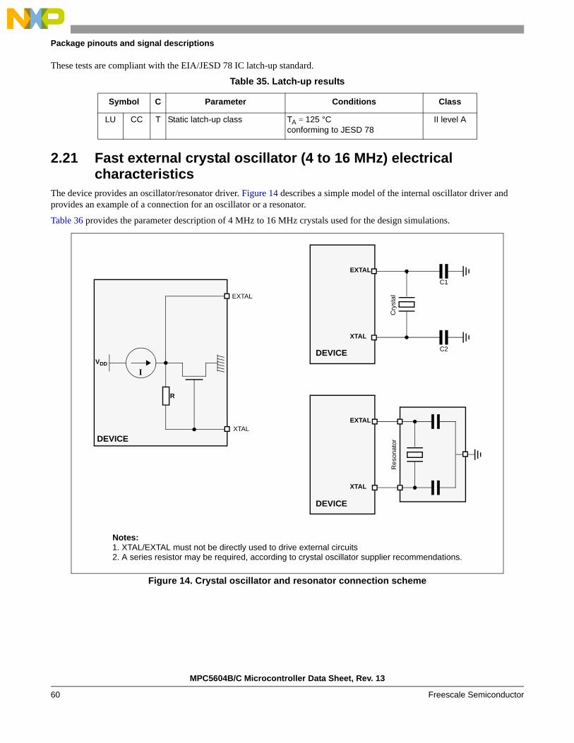
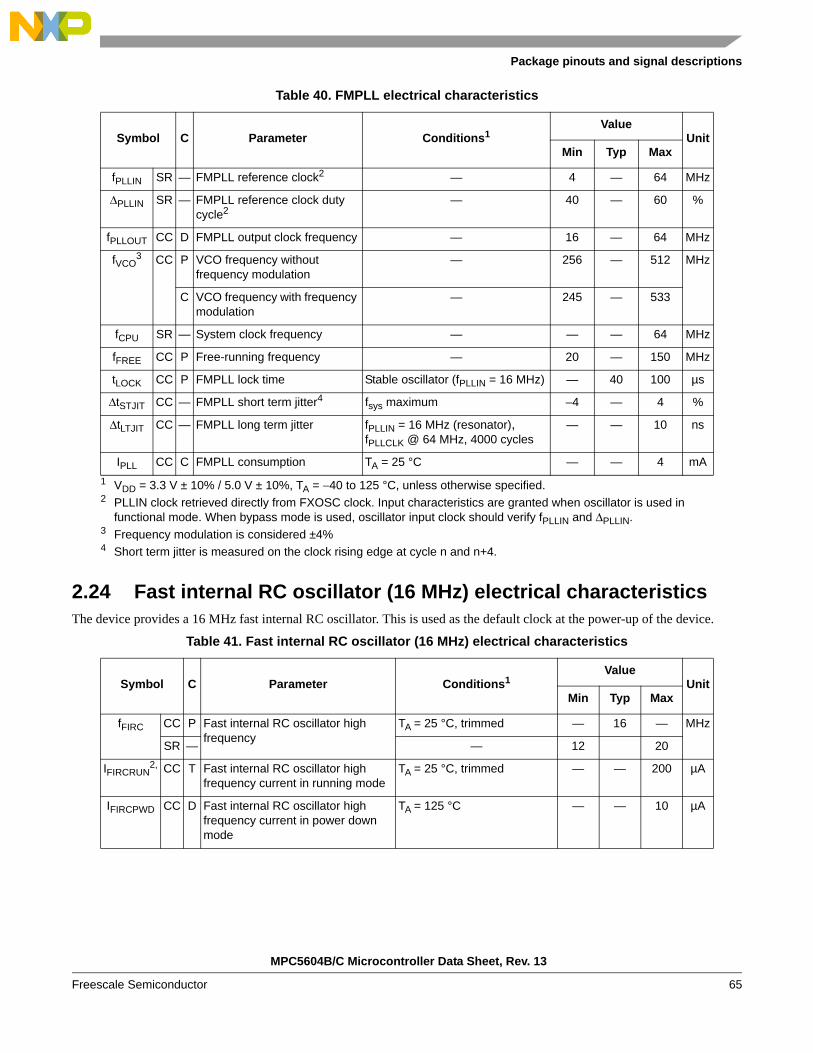
2.15.2 I/O input DC characteristicsTable 15 provides input DC electrical characteristics as described in Figure 7.
Figure 7. I/O input DC electrical characteristics definition
Table 15. I/O input DC electrical characteristics
Symbol C Parameter Conditions1
1 VDD = 3.3 V ± 10% / 5.0 V ± 10%, TA = −40 to 125 °C, unless otherwise specified
ValueUnit
Min Typ Max
VIH SR P Input high level CMOS (Schmitt Trigger)
— 0.65VDD — VDD+0.4 V
VIL SR P Input low level CMOS (Schmitt Trigger)
— −0.4 — 0.35VDD
VHYS CC C Input hysteresis CMOS (Schmitt Trigger)
— 0.1VDD — —
ILKG CC D Digital input leakage No injection on adjacent pin
TA = −40 °C — 2 200 nA
D TA = 25 °C — 2 200
D TA = 85 °C — 5 300
D TA = 105 °C — 12 500
P TA = 125 °C — 70 1000
WFI2
2 In the range from 40 to 1000 ns, pulses can be filtered or not filtered, according to operating temperature and voltage.
SR P Wakeup input filtered pulse — — — 40 ns
WNFI2 SR P Wakeup input not filtered pulse — 1000 — — ns
VIL
VIN
VIH
PDIx = ‘1’
VDD
VHYS
(GPDI register of SIUL)
PDIx = ‘0’
MPC5604B/C Microcontroller Data Sheet, Rev. 13
Package pinouts and signal descriptions
Freescale Semiconductor38
2.15.3 I/O output DC characteristicsThe following tables provide DC characteristics for bidirectional pads:
• Table 16 provides weak pull figures. Both pull-up and pull-down resistances are supported.
• Table 17 provides output driver characteristics for I/O pads when in SLOW configuration.
• Table 18 provides output driver characteristics for I/O pads when in MEDIUM configuration.
• Table 19 provides output driver characteristics for I/O pads when in FAST configuration.
Table 16. I/O pull-up/pull-down DC electrical characteristics
Symbol C Parameter Conditions1
1 VDD = 3.3 V ± 10% / 5.0 V ± 10%, TA = −40 to 125 °C, unless otherwise specified.
2 The configuration PAD3V5 = 1 when VDD = 5 V is only a transient configuration during power-up. All pads but RESET and Nexus output (MDOx, EVTO, MCKO) are configured in input or in high impedance state.
10 — 250
P VIN = VIL, VDD = 3.3 V ± 10% PAD3V5V = 1 10 — 150
2 The configuration PAD3V5 = 1 when VDD = 5 V is only a transient configuration during power-up. All pads but RESET and Nexus output (MDOx, EVTO, MCKO) are configured in input or in high impedance state.
0.8VDD — —
C IOH = −1 mA,VDD = 3.3 V ± 10%, PAD3V5V = 1(recommended)
P IOH = −2 mA,VDD = 5.0 V ± 10%, PAD3V5V = 0(recommended)
0.8VDD — —
C IOH = −1 mA,VDD = 5.0 V ± 10%, PAD3V5V = 12
2 The configuration PAD3V5 = 1 when VDD = 5 V is only a transient configuration during power-up. All pads but RESET and Nexus output (MDOx, EVTO, MCKO) are configured in input or in high impedance state.
0.8VDD — —
C IOH = −1 mA,VDD = 3.3 V ± 10%, PAD3V5V = 1 (recommended)
C IOL = 11mA,VDD = 3.3 V ± 10%, PAD3V5V = 1 (recommended)
— — 0.5
1 VDD = 3.3 V ± 10% / 5.0 V ± 10%, TA = −40 to 125 °C, unless otherwise specified2 The configuration PAD3V5 = 1 when VDD = 5 V is only a transient configuration during power-up. All pads but
RESET and Nexus output (MDOx, EVTO, MCKO) are configured in input or in high impedance state.
Table 20. Output pin transition times
Symbol C Parameter Conditions1
1 VDD = 3.3 V ± 10% / 5.0 V ± 10%, TA = −40 to 125 °C, unless otherwise specified
Table 19. FAST configuration output buffer electrical characteristics (continued)
Symbol C Parameter Conditions1Value
UnitMin Typ Max
Package pinouts and signal descriptions
MPC5604B/C Microcontroller Data Sheet, Rev. 13
Freescale Semiconductor 41
2.15.5 I/O pad current specificationThe I/O pads are distributed across the I/O supply segment. Each I/O supply segment is associated to a VDD/VSS supply pair as described in Table 21.
Table 22 provides I/O consumption figures.
In order to ensure device reliability, the average current of the I/O on a single segment should remain below the IAVGSEG maximum value.
2 CL includes device and package capacitances (CPKG < 5 pF).
Table 21. I/O supply segment
PackageSupply segment
1 2 3 4 5 6
208 MAPBGA1
1 208 MAPBGA available only as development package for Nexus2+
Equivalent to 144 LQFP segment pad distribution MCKO MDOn/MSEO
IRMSSLW CC D Root mean square I/O current for SLOW configuration
CL = 25 pF, 2 MHz VDD = 5.0 V ± 10%,PAD3V5V = 0
— — 2.3 mA
CL = 25 pF, 4 MHz — — 3.2
CL = 100 pF, 2 MHz — — 6.6
CL = 25 pF, 2 MHz VDD = 3.3 V ± 10%,PAD3V5V = 1
— — 1.6
CL = 25 pF, 4 MHz — — 2.3
CL = 100 pF, 2 MHz — — 4.7
MPC5604B/C Microcontroller Data Sheet, Rev. 13
Package pinouts and signal descriptions
Freescale Semiconductor42
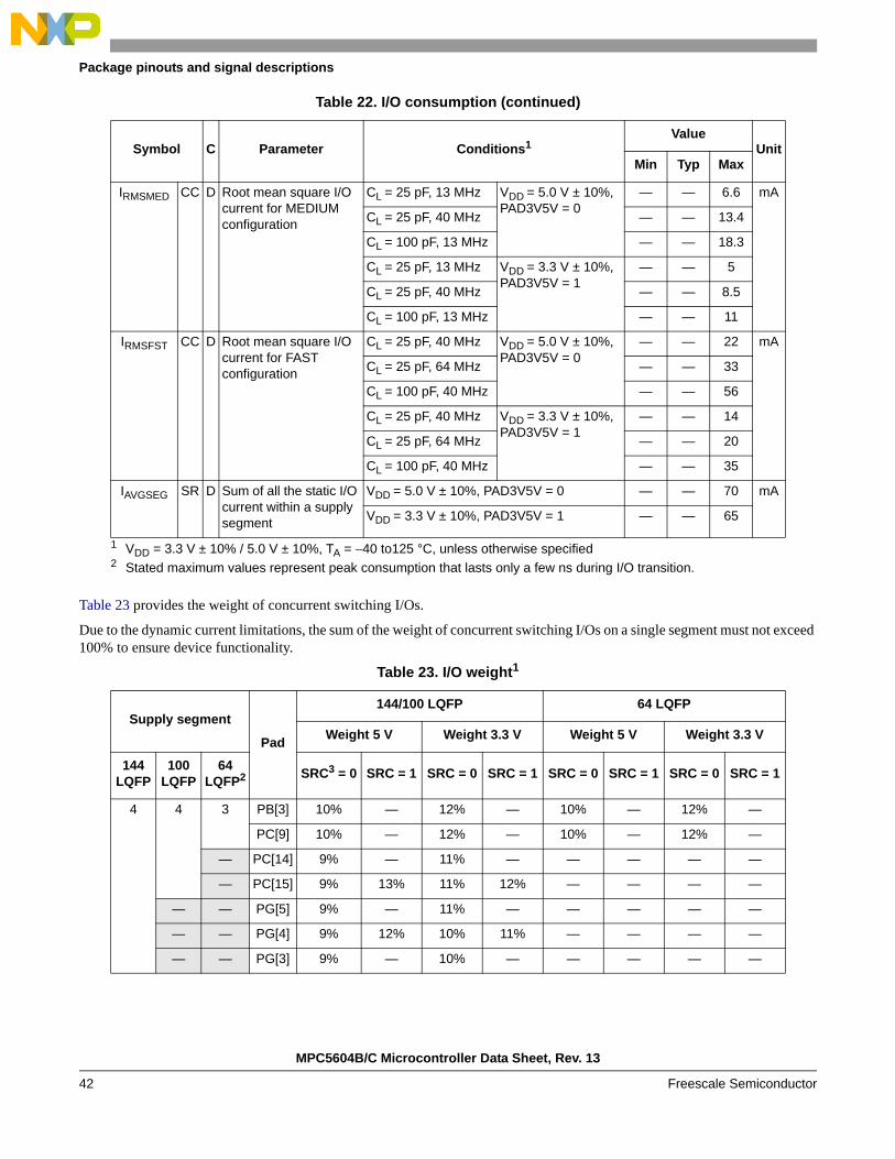
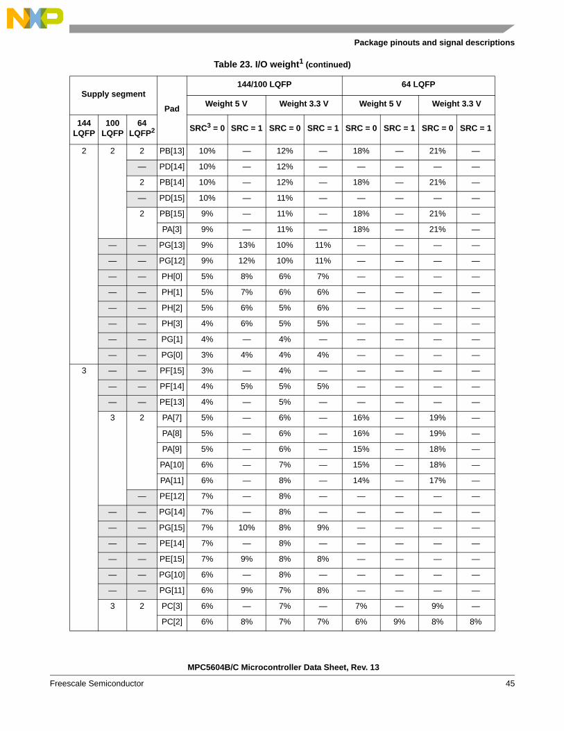
Table 23 provides the weight of concurrent switching I/Os.
Due to the dynamic current limitations, the sum of the weight of concurrent switching I/Os on a single segment must not exceed 100% to ensure device functionality.
IRMSMED CC D Root mean square I/O current for MEDIUM configuration
CL = 25 pF, 13 MHz VDD = 5.0 V ± 10%, PAD3V5V = 0
— — 6.6 mA
CL = 25 pF, 40 MHz — — 13.4
CL = 100 pF, 13 MHz — — 18.3
CL = 25 pF, 13 MHz VDD = 3.3 V ± 10%, PAD3V5V = 1
— — 5
CL = 25 pF, 40 MHz — — 8.5
CL = 100 pF, 13 MHz — — 11
IRMSFST CC D Root mean square I/O current for FAST configuration
CL = 25 pF, 40 MHz VDD = 5.0 V ± 10%, PAD3V5V = 0
— — 22 mA
CL = 25 pF, 64 MHz — — 33
CL = 100 pF, 40 MHz — — 56
CL = 25 pF, 40 MHz VDD = 3.3 V ± 10%, PAD3V5V = 1
— — 14
CL = 25 pF, 64 MHz — — 20
CL = 100 pF, 40 MHz — — 35
IAVGSEG SR D Sum of all the static I/O current within a supply segment
VDD = 5.0 V ± 10%, PAD3V5V = 0 — — 70 mA
VDD = 3.3 V ± 10%, PAD3V5V = 1 — — 65
1 VDD = 3.3 V ± 10% / 5.0 V ± 10%, TA = −40 to125 °C, unless otherwise specified2 Stated maximum values represent peak consumption that lasts only a few ns during I/O transition.
1 VDD = 3.3 V ± 10% / 5.0 V ± 10%, TA = −40 to125 °C, unless otherwise specified2 Segments shown apply to MPC560xB devices only3 SRC: “Slew Rate Control” bit in SIU_PCR
2.17.1 Voltage regulator electrical characteristicsThe device implements an internal voltage regulator to generate the low voltage core supply VDD_LV from the high voltage ballast supply VDD_BV. The regulator itself is supplied by the common I/O supply VDD. The following supplies are involved:
VIL SR P Input low Level CMOS (Schmitt Trigger)
— −0.4 — 0.35VDD V
VHYS CC C Input hysteresis CMOS (Schmitt Trigger)
— 0.1VDD — — V
VOL CC P Output low level Push Pull, IOL = 2mA,VDD = 5.0 V ± 10%, PAD3V5V = 0(recommended)
— — 0.1VDD V
C Push Pull, IOL = 1mA,VDD = 5.0 V ± 10%, PAD3V5V = 12
— — 0.1VDD
C Push Pull, IOL = 1mA,VDD = 3.3 V ± 10%, PAD3V5V = 1 (recommended)
— — 0.5
ttr CC D Output transition time output pin3
CL = 25pF,VDD = 5.0 V ± 10%, PAD3V5V = 0
— — 10 ns
CL = 50pF,VDD = 5.0 V ± 10%, PAD3V5V = 0
— — 20
CL = 100pF,VDD = 5.0 V ± 10%, PAD3V5V = 0
— — 40
CL = 25pF,VDD = 3.3 V ± 10%, PAD3V5V = 1
— — 12
CL = 50pF,VDD = 3.3 V ± 10%, PAD3V5V = 1
— — 25
CL = 100pF,VDD = 3.3 V ± 10%, PAD3V5V = 1
— — 40
WFRST SR P RESET input filtered pulse
— — — 40 ns
WNFRST SR P RESET input not filtered pulse
— 1000 — — ns
|IWPU| CC P Weak pull-up current absolute value
VDD = 3.3 V ± 10%, PAD3V5V = 1 10 — 150 µA
D VDD = 5.0 V ± 10%, PAD3V5V = 0 10 — 150
P VDD = 5.0 V ± 10%, PAD3V5V = 12 10 — 250
1 VDD = 3.3 V ± 10% / 5.0 V ± 10%, TA = −40 to 125 °C, unless otherwise specified2 This transient configuration does not occurs when device is used in the VDD = 3.3 V ± 10% range.3 CL includes device and package capacitance (CPKG < 5 pF).
• HV—High voltage external power supply for voltage regulator module. This must be provided externally through VDD_HV power pin.
• BV—High voltage external power supply for internal ballast module. This must be provided externally through VDD_BV power pin. Voltage values should be aligned with VDD.
• LV—Low voltage internal power supply for core, FMPLL and flash digital logic. This is generated by the internal voltage regulator but provided outside to connect stability capacitor. It is further split into four main domains to ensure noise isolation between critical LV modules within the device:
— LV_COR—Low voltage supply for the core. It is also used to provide supply for FMPLL through double bonding.
— LV_CFLA—Low voltage supply for code flash module. It is supplied with dedicated ballast and shorted to LV_COR through double bonding.
— LV_DFLA—Low voltage supply for data flash module. It is supplied with dedicated ballast and shorted to LV_COR through double bonding.
— LV_PLL—Low voltage supply for FMPLL. It is shorted to LV_COR through double bonding.
Figure 10. Voltage regulator capacitance connection
The internal voltage regulator requires external capacitance (CREGn) to be connected to the device in order to provide a stable low voltage digital supply to the device. Capacitances should be placed on the board as near as possible to the associated pins. Care should also be taken to limit the serial inductance of the board to less than 5 nH.
Each decoupling capacitor must be placed between each of the three VDD_LV/VSS_LV supply pairs to ensure stable voltage (see Section 2.13, Recommended operating conditions).
The internal voltage regulator requires a controlled slew rate of both VDD_HV and VDD_BV as described in Figure 11.
CR
EG
1 (L
V_
CO
R/L
V_
DF
LA
)
DEVICE
VSS_LV
VDD_BV
VDD_LV
CD
EC
1 (B
alla
st d
eco
upl
ing
)
VSS_LV VDD_LV VDD_HV
VSS_LV VDD_LV
CREG2 (LV_COR/LV_CFLA)
CREG3 CDEC2
DEVICE
VDD_BV
I
VDD_LVn
VREF
VDD_HV
Voltage Regulator
VSS_HVVSS_LVn
(supply/IO decoupling)(LV_COR/LV_PLL)
MPC5604B/C Microcontroller Data Sheet, Rev. 13
Package pinouts and signal descriptions
Freescale Semiconductor50
Figure 11. VDD_HV and VDD_BV maximum slope
When STANDBY mode is used, further constraints are applied to the both VDD_HV and VDD_BV in order to guarantee correct regulator function during STANDBY exit. This is described on Figure 12.
STANDBY regulator constraints should normally be guaranteed by implementing equivalent of CSTDBY capacitance on application board (capacitance and ESR typical values), but would actually depend on exact characteristics of application external regulator.
Figure 12. VDD_HV and VDD_BV supply constraints during STANDBY mode exit
VDD_HV
tdd VDD
POWER UP POWER DOWN
VDD_HV(MAX)
FUNCTIONAL RANGE
VDD_HV(MIN)
VDD_HV
VDD_HV(MIN)
ΔVDD(STDBY)
VDD_HV
VDD_HV(MAX)
VDD_LV
tdd VDD STDBY( )
tdd VDD STDBY( )
ΔVDD(STDBY)
VDD_LV(NOMINAL)
0V
Package pinouts and signal descriptions
MPC5604B/C Microcontroller Data Sheet, Rev. 13
Freescale Semiconductor 51
Table 25. Voltage regulator electrical characteristics
Symbol C Parameter Conditions1Value
UnitMin Typ Max
CREGn SR — Internal voltage regulator external capacitance
— 200 — 500 nF
RREG SR — Stability capacitor equivalent serial resistance
Range:10 kHz to 20 MHz
— — 0.2 Ω
CDEC1 SR — Decoupling capacitance2 ballast VDD_BV/VSS_LV pair:VDD_BV = 4.5 V to 5.5 V
1003 4704 — nF
VDD_BV/VSS_LV pair:VDD_BV = 3 V to 3.6 V
400 —
CDEC2 SR — Decoupling capacitance regulator supply
VDD/VSS pair 10 100 — nF
SR — Maximum slope on VDD — — 250 mV/µs
|ΔVDD(STDBY)| SR — Maximum instant variation on VDD during standby exit
— — 30 mV
SR — Maximum slope on VDD during standby exit
— — 15 mV/µs
VMREG CC T Main regulator output voltage Before exiting from reset
— 1.32 — V
P After trimming 1.16 1.28 —
IMREG SR — Main regulator current provided to VDD_LV domain
— — — 150 mA
IMREGINT CC D Main regulator module current consumption
IMREG = 200 mA — — 2 mA
IMREG = 0 mA — — 1
VLPREG CC P Low power regulator output voltage
After trimming 1.16 1.28 — V
ILPREG SR — Low power regulator current provided to VDD_LV domain
—— — 15 mA
ILPREGINT CC D Low power regulator module current consumption
ILPREG = 15 mA;TA = 55 °C
— — 600 µA
— ILPREG = 0 mA;TA = 55 °C
— 5 —
VULPREG CC P Ultra low power regulator output voltage
After trimming 1.16 1.28 — V
IULPREG SR — Ultra low power regulator current provided to VDD_LV domain
— — — 5 mA
IULPREGINT CC D Ultra low power regulator module current consumption
IULPREG = 5 mA;TA = 55 °C
— — 100 µA
IULPREG = 0 mA;TA = 55 °C
— 2 —
tdd VDD
tdd VDD STDBY( )
MPC5604B/C Microcontroller Data Sheet, Rev. 13
Package pinouts and signal descriptions
Freescale Semiconductor52
The |ΔVDD(STDBY)| and dVDD(STDBY)/dt system requirement can be used to define the component used for the VDD supply generation. The following two examples describe how to calculate capacitance size:
Example 1. No regulator (worst case)
The |ΔVDD(STDBY)| parameter can be seen as the VDD voltage drop through the ESR resistance of the regulator stability capacitor when the IDD_BV current required to load VDD_LV domain during the standby exit. It is thus possible to define the maximum equivalent resistance ESRSTDBY(MAX) of the total capacitance on the VDD supply:
The dVDD(STDBY)/dt parameter can be seen as the VDD voltage drop at the capacitance pin (excluding ESR drop) while providing the IDD_BV supply required to load VDD_LV domain during the standby exit. It is thus possible to define the minimum equivalent capacitance CSTDBY(MIN) of the total capacitance on the VDD supply:
This configuration is a worst case, with the assumption no regulator is available.
Example 2. Simplified regulator
The regulator should be able to provide significant amount of the current during the standby exit process. For example, in case of an ideal voltage regulator providing 200 mA current, it is possible to recalculate the equivalent ESRSTDBY(MAX) and CSTDBY(MIN) as follows:
In case optimization is required, CSTDBY(MIN) and ESRSTDBY(MAX) should be calculated based on the regulator characteristics as well as the board VDD plane characteristics.
2.17.2 Low voltage detector electrical characteristicsThe device implements a Power-on Reset (POR) module to ensure correct power-up initialization, as well as four low voltage detectors (LVDs) to monitor the VDD and the VDD_LV voltage while device is supplied:
IDD_BV CC D In-rush average current on VDD_BV during power-up5
— — — 3006 mA
1 VDD = 3.3 V ± 10% / 5.0 V ± 10%, TA = −40 to 125 °C, unless otherwise specified2 This capacitance value is driven by the constraints of the external voltage regulator supplying the VDD_BV voltage.
A typical value is in the range of 470 nF.3 This value is acceptable to guarantee operation from 4.5 V to 5.5 V4 External regulator and capacitance circuitry must be capable of providing IDD_BV while maintaining supply VDD_BV
in operating range.5 In-rush average current is seen only for short time (maximum 20 µs) during power-up and on standby exit. It is
dependant on the sum of the CREGn capacitances.6 The duration of the in-rush current depends on the capacitance placed on LV pins. BV decoupling capacitors must
be sized accordingly. Refer to IMREG value for minimum amount of current to be provided in cc.
1. Based on typical time for standby exit sequence of 20 µs, ESR(MIN) can actually be considered at ~50 kHz.
Table 25. Voltage regulator electrical characteristics (continued)
Symbol C Parameter Conditions1Value
UnitMin Typ Max
Package pinouts and signal descriptions
MPC5604B/C Microcontroller Data Sheet, Rev. 13
Freescale Semiconductor 53
• POR monitors VDD during the power-up phase to ensure device is maintained in a safe reset state (refer to RGM Destructive Event Status (RGM_DES) Register flag F_POR in device reference manual)
• LVDHV3 monitors VDD to ensure device reset below minimum functional supply (refer to RGM Destructive Event Status (RGM_DES) Register flag F_LVD27 in device reference manual)
• LVDHV5 monitors VDD when application uses device in the 5.0 V ± 10% range (refer to RGM Functional Event Status (RGM_FES) Register flag F_LVD45 in device reference manual)
• LVDLVCOR monitors power domain No. 1 (refer to RGM Destructive Event Status (RGM_DES) Register flag F_LVD12_PD1 in device reference manual
• LVDLVBKP monitors power domain No. 0 (refer to RGM Destructive Event Status (RGM_DES) Register flag F_LVD12_PD0 in device reference manual)
NOTEWhen enabled, power domain No. 2 is monitored through LVDLVBKP.
Figure 13. Low voltage detector vs reset
NOTEFigure 13 (Low voltage detector vs reset) does not apply to LVDHV5 low voltage detector because LVDHV5 is automatically disabled during reset and it must be enabled by software again. Once the device is forced to reset by LVDHV5, the LVDHV5 is disabled and reset is released as soon as internal reset sequence is completed regardless of LVDHV5H threshold.
VDD
VLVDHVxH
RESET
VLVDHVxL
MPC5604B/C Microcontroller Data Sheet, Rev. 13
Package pinouts and signal descriptions
Freescale Semiconductor54
2.18 Power consumptionTable 27 provides DC electrical characteristics for significant application modes. These values are indicative values; actual consumption depends on the application.
Table 26. Low voltage detector electrical characteristics
Symbol C Parameter Conditions1
1 VDD = 3.3 V ± 10% / 5.0 V ± 10%, TA = −40 to 125 °C, unless otherwise specified
ValueUnit
Min Typ Max
VPORUP SR P Supply for functional POR module — 1.0 — 5.5 V
VPORH CC P Power-on reset threshold TA = 25 °C,after trimming
1.5 — 2.6
T — 1.5 — 2.6
VLVDHV3H CC T LVDHV3 low voltage detector high threshold — — — 2.95
VLVDHV3L CC P LVDHV3 low voltage detector low threshold 2.6 — 2.9
VLVDHV5H CC T LVDHV5 low voltage detector high threshold — — 4.5
VLVDHV5L CC P LVDHV5 low voltage detector low threshold 3.8 — 4.4
VLVDLVCORL CC P LVDLVCOR low voltage detector low threshold 1.08 — 1.16
VLVDLVBKPL CC P LVDLVBKP low voltage detector low threshold 1.08 — 1.16
Table 27. Power consumption on VDD_BV and VDD_HV
Symbol C Parameter Conditions1Value
UnitMin Typ Max
IDDMAX2 CC D RUN mode maximum
average current— — 115 1403 mA
IDDRUN4 CC T RUN mode typical
average current5fCPU = 8 MHz — 7 — mA
T fCPU = 16 MHz — 18 —
T fCPU = 32 MHz — 29 —
P fCPU = 48 MHz — 40 100
P fCPU = 64 MHz — 51 125
IDDHALT CC C HALT mode current6 Slow internal RC oscillator (128 kHz) running
TA = 25 °C — 8 15 mA
P TA = 125 °C — 14 25
IDDSTOP CC P STOP mode current7 Slow internal RC oscillator (128 kHz) running
TA = 25 °C — 180 7008 µA
D TA = 55 °C — 500 —
D TA = 85 °C — 1 68 mA
D TA = 105 °C — 2 98
P TA = 125 °C — 4.5 128
Package pinouts and signal descriptions
MPC5604B/C Microcontroller Data Sheet, Rev. 13
Freescale Semiconductor 55
IDDSTDBY2 CC P STANDBY2 mode current9
Slow internal RC oscillator (128 kHz) running
TA = 25 °C — 30 100 µA
D TA = 55 °C — 75 —
D TA = 85 °C — 180 700
D TA = 105 °C — 315 1000
P TA = 125 °C — 560 1700
IDDSTDBY1 CC T STANDBY1 mode current10
Slow internal RC oscillator (128 kHz) running
TA = 25 °C — 20 60 µA
D TA = 55 °C — 45 —
D TA = 85 °C — 100 350
D TA = 105 °C — 165 500
D TA = 125 °C — 280 900
1 VDD = 3.3 V ± 10% / 5.0 V ± 10%, TA = −40 to 125 °C, unless otherwise specified2 IDDMAX is drawn only from the VDD_BV pin. Running consumption does not include I/Os toggling which is highly
dependent on the application. The given value is thought to be a worst case value with all peripherals running, and code fetched from code flash while modify operation ongoing on data flash. Notice that this value can be significantly reduced by application: switch off not used peripherals (default), reduce peripheral frequency through internal prescaler, fetch from RAM most used functions, use low power mode when possible.
3 Higher current may be sinked by device during power-up and standby exit. Please refer to in rush current on Table 25.4 IDDRUN is drawn only from the VDD_BV pin. RUN current measured with typical application with accesses on both flash
and RAM.5 Only for the “P” classification: Data and Code Flash in Normal Power. Code fetched from RAM: Serial IPs CAN and
LIN in loop back mode, DSPI as Master, PLL as system Clock (4 x Multiplier) peripherals on (eMIOS/CTU/ADC) and running at max frequency, periodic SW/WDG timer reset enabled.
6 Data Flash Power Down. Code Flash in Low Power. SIRC (128 kHz) and FIRC (16 MHz) on. 10 MHz XTAL clock. FlexCAN: instances: 0, 1, 2 ON (clocked but not reception or transmission), instances: 4, 5, 6 clock gated. LINFlex: instances: 0, 1, 2 ON (clocked but not reception or transmission), instance: 3 clock gated. eMIOS: instance: 0 ON (16 channels on PA[0]–PA[11] and PC[12]–PC[15]) with PWM 20 kHz, instance: 1 clock gated. DSPI: instance: 0 (clocked but no communication). RTC/API ON. PIT ON. STM ON. ADC ON but not conversion except 2 analog watchdog.
7 Only for the “P” classification: No clock, FIRC (16 MHz) off, SIRC (128 kHz) on, PLL off, HPvreg off, ULPVreg/LPVreg on. All possible peripherals off and clock gated. Flash in power down mode.
8 When going from RUN to STOP mode and the core consumption is > 6 mA, it is normal operation for the main regulator module to be kept on by the on-chip current monitoring circuit. This is most likely to occur with junction temperatures exceeding 125 °C and under these circumstances, it is possible for the current to initially exceed the maximum STOP specification by up to 2 mA. After entering stop, the application junction temperature will reduce to the ambient level and the main regulator will be automatically switched off when the load current is below 6 mA.
9 Only for the “P” classification: ULPreg on, HP/LPVreg off, 32 KB RAM on, device configured for minimum consumption, all possible modules switched off.
10 ULPreg on, HP/LPVreg off, 8 KB RAM on, device configured for minimum consumption, all possible modules switched off.
Table 27. Power consumption on VDD_BV and VDD_HV (continued)
Symbol C Parameter Conditions1Value
UnitMin Typ Max
MPC5604B/C Microcontroller Data Sheet, Rev. 13
Package pinouts and signal descriptions
Freescale Semiconductor56
2.19 Flash memory electrical characteristics
2.19.1 Program/Erase characteristicsTable 28 shows the program and erase characteristics.
ECC circuitry provides correction of single bit faults and is used to improve further automotive reliability results. Some units will experience single bit corrections throughout the life of the product with no impact to product reliability.
Table 28. Program and erase specifications
Symbol C Parameter
Value
UnitMin Typ1
1 Typical program and erase times assume nominal supply values and operation at 25 °C.
3 The maximum program and erase times occur after the specified number of program/erase cycles. These maximum values are characterized but not guaranteed.
Tdwprogram CC C Double word (64 bits) program time4
4 Actual hardware programming times. This does not include software overhead.
— 22 50 500 µs
T16Kpperase 16 KB block preprogram and erase time — 300 500 5000 ms
T32Kpperase 32 KB block preprogram and erase time — 400 600 5000 ms
T128Kpperase 128 KB block preprogram and erase time — 800 1300 7500 ms
Tesus CC D Erase suspend latency — — 30 30 µs
Table 29. Flash module life
Symbol C Parameter ConditionsValue
UnitMin Typ Max
P/E CC C Number of program/erase cycles per block over the operating temperature range (TJ)
16 KB blocks 100,000 — — cycles
32 KB blocks 10,000 100,000 —
128 KB blocks 1,000 100,000 —
Retention CC C Minimum data retention at 85 °C average ambient temperature1
1 Ambient temperature averaged over duration of application, not to exceed recommended product operating temperature range.
Blocks with0–1,000 P/E cycles
20 — — years
Blocks with1,001–10,000 P/E cycles
10 — —
Blocks with10,001–100,000 P/E cycles
5 — —
Package pinouts and signal descriptions
MPC5604B/C Microcontroller Data Sheet, Rev. 13
Freescale Semiconductor 57
2.19.2 Flash power supply DC characteristicsTable 31 shows the power supply DC characteristics on external supply.
Table 30. Flash read access timing
Symbol C Parameter Conditions1
1 VDD = 3.3 V ± 10% / 5.0 V ± 10%, TA = −40 to 125 °C, unless otherwise specified
Max Unit
fREAD CC P Maximum frequency for Flash reading 2 wait states 64 MHz
C 1 wait state 40
C 0 wait states 20
Table 31. Flash memory power supply DC electrical characteristics
Symbol C Parameter Conditions1
1 VDD = 3.3 V ± 10% / 5.0 V ± 10%, TA = −40 to 125 °C, unless otherwise specified
ValueUnit
Min Typ Max
IFREAD2
2 This value is only relative to the actual duration of the read cycle
CC D Sum of the current consumption on VDD_HV and VDD_BV on read access
Code flash memory module readfCPU = 64 MHz3
3 fCPU 64 MHz can be achieved only at up to 105 °C
— 15 33 mA
Data flash memory module readfCPU = 64 MHz3
— 15 33
IFMOD2 CC D Sum of the current consumption on
VDD_HV and VDD_BV on matrix modification (program/erase)
Program/Erase ongoing while reading data flash memory registers fCPU = 64 MHz3
— 15 33
IFLPW CC D Sum of the current consumption on VDD_HV and VDD_BV
During code flash memory low-power mode
— — 900 µA
During data flash memory low-power mode
— — 900
IFPWD CC D Sum of the current consumption on VDD_HV and VDD_BV
During code flash memory power-down mode
— — 150 µA
During data flash memory power-down mode
— — 150
MPC5604B/C Microcontroller Data Sheet, Rev. 13
Package pinouts and signal descriptions
Freescale Semiconductor58
2.19.3 Start-up/Switch-off timings
2.20 Electromagnetic compatibility (EMC) characteristicsSusceptibility tests are performed on a sample basis during product characterization.
2.20.1 Designing hardened software to avoid noise problemsEMC characterization and optimization are performed at component level with a typical application environment and simplified MCU software. It should be noted that good EMC performance is highly dependent on the user application and the software in particular.
Therefore it is recommended that the user apply EMC software optimization and prequalification tests in relation with the EMC level requested for his application.
• Software recommendations: The software flowchart must include the management of runaway conditions such as:
— Corrupted program counter
— Unexpected reset
— Critical data corruption (control registers...)
• Prequalification trials: Most of the common failures (unexpected reset and program counter corruption) can be reproduced by manually forcing a low state on the reset pin or the oscillator pins for 1 second.
To complete these trials, ESD stress can be applied directly on the device. When unexpected behavior is detected, the software can be hardened to prevent unrecoverable errors occurring.
2.20.2 Electromagnetic interference (EMI)The product is monitored in terms of emission based on a typical application. This emission test conforms to the IEC 61967-1 standard, which specifies the general conditions for EMI measurements.
Table 32. Start-up time/Switch-off time
Symbol C Parameter Conditions1
1 VDD = 3.3 V ± 10% / 5.0 V ± 10%, TA = −40 to 125 °C, unless otherwise specified
ValueUnit
Min Typ Max
TFLARSTEXIT CC T Delay for Flash module to exit reset mode Code Flash — — 125 µs
T Data Flash — — 125
TFLALPEXIT CC T Delay for Flash module to exit low-power mode
Code Flash — — 0.5
T Data Flash — — 0.5
TFLAPDEXIT CC T Delay for Flash module to exit power-down mode
Code Flash — — 30
T Data Flash — — 30
TFLALPENTRY CC T Delay for Flash module to enter low-power mode
Code Flash — — 0.5
T Data Flash — — 0.5
TFLAPDENTRY CC T Delay for Flash module to enter power-down mode
Code Flash — — 1.5
T Data Flash — — 1.5
Package pinouts and signal descriptions
MPC5604B/C Microcontroller Data Sheet, Rev. 13
Freescale Semiconductor 59
2.20.3 Absolute maximum ratings (electrical sensitivity)Based on two different tests (ESD and LU) using specific measurement methods, the product is stressed in order to determine its performance in terms of electrical sensitivity.
2.20.3.1 Electrostatic discharge (ESD)
Electrostatic discharges (a positive then a negative pulse separated by 1 second) are applied to the pins of each sample according to each pin combination. The sample size depends on the number of supply pins in the device (3 parts*(n+1) supply pin). This test conforms to the AEC-Q100-002/-003/-011 standard.
2.20.3.2 Static latch-up (LU)
Two complementary static tests are required on six parts to assess the latch-up performance:
• A supply overvoltage is applied to each power supply pin.
• A current injection is applied to each input, output and configurable I/O pin.
Table 33. EMI radiated emission measurement1,2
1 EMI testing and I/O port waveforms per IEC 61967-1, -2, -42 For information on conducted emission and susceptibility measurement (norm IEC 61967-4), please contact your
local marketing representative.
Symbol C Parameter ConditionsValue
UnitMin Typ Max
— SR — Scan range — 0.150 — 1000 MHz
fCPU SR — Operating frequency — — 64 — MHz
VDD_LV SR — LV operating voltages — — 1.28 — V
SEMI CC T Peak level VDD = 5 V, TA = 25 °C,LQFP144 packageTest conforming to IEC 61967-2,fOSC = 8 MHz/fCPU = 64 MHz
No PLL frequency modulation
— — 18 dBµV
±2% PLL frequencymodulation
— — 14 dBµV
Table 34. ESD absolute maximum ratings1 2
1 All ESD testing is in conformity with CDF-AEC-Q100 Stress Test Qualification for Automotive Grade Integrated Circuits.
2 A device will be defined as a failure if after exposure to ESD pulses the device no longer meets the device specification requirements. Complete DC parametric and functional testing shall be performed per applicable device specification at room temperature followed by hot temperature, unless specified otherwise in the device specification.
Symbol C Ratings Conditions Class Max value Unit
VESD(HBM) CC T Electrostatic discharge voltage(Human Body Model)
TA = 25 °Cconforming to AEC-Q100-002
H1C 2000 V
VESD(MM) CC T Electrostatic discharge voltage(Machine Model)
TA = 25 °Cconforming to AEC-Q100-003
M2 200
VESD(CDM) CC T Electrostatic discharge voltage(Charged Device Model)
TA = 25 °Cconforming to AEC-Q100-011
C3A 500
750 (corners)
MPC5604B/C Microcontroller Data Sheet, Rev. 13
Package pinouts and signal descriptions
Freescale Semiconductor60
These tests are compliant with the EIA/JESD 78 IC latch-up standard.
2.21 Fast external crystal oscillator (4 to 16 MHz) electrical characteristics
The device provides an oscillator/resonator driver. Figure 14 describes a simple model of the internal oscillator driver and provides an example of a connection for an oscillator or a resonator.
Table 36 provides the parameter description of 4 MHz to 16 MHz crystals used for the design simulations.
Figure 14. Crystal oscillator and resonator connection scheme
Table 35. Latch-up results
Symbol C Parameter Conditions Class
LU CC T Static latch-up class TA = 125 °Cconforming to JESD 78
II level A
C2
C1
Cry
stal
XTAL
EXTAL
Re
son
ator
XTAL
EXTAL
DEVICE
DEVICE
DEVICEXTAL
EXTAL
I
R
VDD
2. A series resistor may be required, according to crystal oscillator supplier recommendations.1. XTAL/EXTAL must not be directly used to drive external circuitsNotes:
Package pinouts and signal descriptions
MPC5604B/C Microcontroller Data Sheet, Rev. 13
Freescale Semiconductor 61
Figure 15. Fast external crystal oscillator (4 to 16 MHz) timing diagram
Table 36. Crystal description
Nominalfrequency
(MHz)
NDK crystal reference
Crystalequivalent
seriesresistance
ESR Ω
Crystalmotional
capacitance(Cm) fF
Crystalmotional
inductance(Lm) mH
Load onxtalin/xtalout
C1 = C2(pF)1
1 The values specified for C1 and C2 are the same as used in simulations. It should be ensured that the testing includes all the parasitics (from the board, probe, crystal, etc.) as the AC / transient behavior depends upon them.
Shuntcapacitance
between xtalout
and xtalinC02 (pF)
2 The value of C0 specified here includes 2 pF additional capacitance for parasitics (to be seen with bond-pads, package, etc.).
4 NX8045GB 300 2.68 591.0 21 2.93
8 NX5032GA 300 2.46 160.7 17 3.01
10 150 2.93 86.6 15 2.91
12 120 3.11 56.5 15 2.93
16 120 3.90 25.3 10 3.00
VFXOSCOP
tFXOSCSU
VXTAL
VFXOSC
valid internal clock
90%
10%
1/fFXOSC
S_MTRANS bit (ME_GS register)
‘1’
‘0’
MPC5604B/C Microcontroller Data Sheet, Rev. 13
Package pinouts and signal descriptions
Freescale Semiconductor62
2.22 Slow external crystal oscillator (32 kHz) electrical characteristicsThe device provides a low power oscillator/resonator driver.
Table 37. Fast external crystal oscillator (4 to 16 MHz) electrical characteristics
Symbol C Parameter Conditions1
1 VDD = 3.3 V ± 10% / 5.0 V ± 10%, TA = −40 to 125 °C, unless otherwise specified
ValueUnit
Min Typ Max
fFXOSC SR — Fast external crystal oscillator frequency
— 4.0 — 16.0 MHz
gmFXOSC CC C Fast external crystaloscillator transconductance
VDD = 3.3 V ± 10%,PAD3V5V = 1OSCILLATOR_MARGIN = 0
2.2 — 8.2 mA/V
CC P VDD = 5.0 V ± 10%,PAD3V5V = 0OSCILLATOR_MARGIN = 0
2.0 — 7.4
CC C VDD = 3.3 V ± 10%,PAD3V5V = 1OSCILLATOR_MARGIN = 1
2.7 — 9.7
CC C VDD = 5.0 V ± 10%,PAD3V5V = 0OSCILLATOR_MARGIN = 1
2.5 — 9.2
VFXOSC CC T Oscillation amplitude at EXTAL
fOSC = 4 MHz,OSCILLATOR_MARGIN = 0
1.3 — — V
fOSC = 16 MHz,OSCILLATOR_MARGIN = 1
1.3 — —
VFXOSCOP CC C Oscillation operating point — — 0.95 — V
IFXOSC,2
2 Stated values take into account only analog module consumption but not the digital contributor (clock tree and enabled peripherals)
CC T Fast external crystal oscillator consumption
— — 2 3 mA
tFXOSCSU CC T Fast external crystal oscillator start-up time
fOSC = 4 MHz,OSCILLATOR_MARGIN = 0
— — 6 ms
fOSC = 16 MHz,OSCILLATOR_MARGIN = 1
— — 1.8
VIH SR P Input high level CMOS(Schmitt Trigger)
Oscillator bypass mode 0.65VDD — VDD+0.4 V
VIL SR P Input low level CMOS(Schmitt Trigger)
Oscillator bypass mode −0.4 — 0.35VDD V
Package pinouts and signal descriptions
MPC5604B/C Microcontroller Data Sheet, Rev. 13
Freescale Semiconductor 63
Figure 16. Crystal oscillator and resonator connection scheme
Figure 17. Equivalent circuit of a quartz crystal
Table 38. Crystal motional characteristics1
1 Crystal used: Epson Toyocom MC306
Symbol Parameter ConditionsValue
UnitMin Typ Max
Lm Motional inductance — — 11.796 — KH
Cm Motional capacitance — — 2 — fF
C1/C2 Load capacitance at OSC32K_XTAL and OSC32K_EXTAL with respect to ground2
2.23 FMPLL electrical characteristicsThe device provides a frequency-modulated phase-locked loop (FMPLL) module to generate a fast system clock from the main oscillator driver.
2 This is the recommended range of load capacitance at OSC32K_XTAL and OSC32K_EXTAL with respect to ground. It includes all the parasitics due to board traces, crystal and package.
3 Maximum ESR (Rm) of the crystal is 50 kΩ4 C0 includes a parasitic capacitance of 2.0 pF between OSC32K_XTAL and OSC32K_EXTAL pins
1 VDD = 3.3 V ± 10% / 5.0 V ± 10%, TA = −40 to 125 °C, unless otherwise specified. Values are specified for no neighbor GPIO pin activity. If oscillator is enabled (OSC32K_XTAL and OSC32K_EXTAL pins), neighboring pins should not toggle.
ValueUnit
Min Typ Max
fSXOSC SR — Slow external crystal oscillator frequency — 32 32.768 40 kHz
VSXOSC CC T Oscillation amplitude — — 2.1 — V
ISXOSCBIAS CC T Oscillation bias current — — 2.5 — µA
ISXOSC CC T Slow external crystal oscillator consumption — — — 8 µA
TSXOSCSU CC T Slow external crystal oscillator start-up time — — — 22
2 Start-up time has been measured with EPSON TOYOCOM MC306 crystal. Variation may be seen with other crystal.
s
OSCON bit (OSC_CTL register)
TSXOSCSU
1
VOSC32K_XTAL
VSXOSC
valid internal clock
90%
10%
1/fSXOSC
0
Package pinouts and signal descriptions
MPC5604B/C Microcontroller Data Sheet, Rev. 13
Freescale Semiconductor 65
2.24 Fast internal RC oscillator (16 MHz) electrical characteristicsThe device provides a 16 MHz fast internal RC oscillator. This is used as the default clock at the power-up of the device.
Table 40. FMPLL electrical characteristics
Symbol C Parameter Conditions1
1 VDD = 3.3 V ± 10% / 5.0 V ± 10%, TA = −40 to 125 °C, unless otherwise specified.
ValueUnit
Min Typ Max
fPLLIN SR — FMPLL reference clock2
2 PLLIN clock retrieved directly from FXOSC clock. Input characteristics are granted when oscillator is used in functional mode. When bypass mode is used, oscillator input clock should verify fPLLIN and ΔPLLIN.
— 4 — 64 MHz
ΔPLLIN SR — FMPLL reference clock duty cycle2
— 40 — 60 %
fPLLOUT CC D FMPLL output clock frequency — 16 — 64 MHz
fVCO3
3 Frequency modulation is considered ±4%
CC P VCO frequency without frequency modulation
— 256 — 512 MHz
C VCO frequency with frequency modulation
— 245 — 533
fCPU SR — System clock frequency — — — 64 MHz
fFREE CC P Free-running frequency — 20 — 150 MHz
tLOCK CC P FMPLL lock time Stable oscillator (fPLLIN = 16 MHz) — 40 100 µs
ΔtSTJIT CC — FMPLL short term jitter4
4 Short term jitter is measured on the clock rising edge at cycle n and n+4.
fsys maximum –4 — 4 %
ΔtLTJIT CC — FMPLL long term jitter fPLLIN = 16 MHz (resonator), fPLLCLK @ 64 MHz, 4000 cycles
— — 10 ns
IPLL CC C FMPLL consumption TA = 25 °C — — 4 mA
Table 41. Fast internal RC oscillator (16 MHz) electrical characteristics
Symbol C Parameter Conditions1Value
UnitMin Typ Max
fFIRC CC P Fast internal RC oscillator high frequency
TA = 25 °C, trimmed — 16 — MHz
SR — — 12 20
IFIRCRUN2, CC T Fast internal RC oscillator high
frequency current in running modeTA = 25 °C, trimmed — — 200 µA
IFIRCPWD CC D Fast internal RC oscillator high frequency current in power down mode
TA = 125 °C — — 10 µA
MPC5604B/C Microcontroller Data Sheet, Rev. 13
Package pinouts and signal descriptions
Freescale Semiconductor66
2.25 Slow internal RC oscillator (128 kHz) electrical characteristicsThe device provides a 128 kHz slow internal RC oscillator. This can be used as the reference clock for the RTC module.
IFIRCSTOP CC T Fast internal RC oscillator high frequency and system clock current in stop mode
TA = 25 °C sysclk = off — 500 — µA
sysclk = 2 MHz — 600 —
sysclk = 4 MHz — 700 —
sysclk = 8 MHz — 900 —
sysclk = 16 MHz — 1250 —
tFIRCSU CC C Fast internal RC oscillator start-up time
VDD = 5.0 V ± 10% — 1.1 2.0 µs
ΔFIRCPRE CC T Fast internal RC oscillator precisionafter software trimming of fFIRC
TA = 25 °C −1 — +1 %
ΔFIRCTRIM CC T Fast internal RC oscillator trimming step
TA = 25 °C — 1.6 %
ΔFIRCVAR CC P Fast internal RC oscillator variation in over temperature and supply with respect to fFIRC at TA = 25 °C in high-frequency configuration
— −5 — +5 %
1 VDD = 3.3 V ± 10% / 5.0 V ± 10%, TA = −40 to 125 °C, unless otherwise specified.2 This does not include consumption linked to clock tree toggling and peripherals consumption when RC oscillator is
1 VDD = 3.3 V ± 10% / 5.0 V ± 10%, TA = −40 to 125 °C, unless otherwise specified.2 This does not include consumption linked to clock tree toggling and peripherals consumption when RC oscillator is
Figure 19. ADC characteristic and error definitions
2.26.2 Input impedance and ADC accuracyIn the following analysis, the input circuit corresponding to the precise channels is considered.
To preserve the accuracy of the A/D converter, it is necessary that analog input pins have low AC impedance. Placing a capacitor with good high frequency characteristics at the input pin of the device can be effective: the capacitor should be as large as
(2)
(1)
(3)
(4)
(5)
Offset error (EO)
Offset error (EO)
Gain error (EG)
1 LSB (ideal)
1023
1022
1021
1020
1019
1018
5
4
3
2
1
0
7
6
1 2 3 4 5 6 7 1017 1018 1019 1020 1021 1022 1023
(1) Example of an actual transfer curve
(2) The ideal transfer curve
(3) Differential non-linearity error (DNL)
(4) Integral non-linearity error (INL)
(5) Center of a step of the actual transfer curve
1 LSB ideal = VDD_ADC / 1024
Vin(A) (LSBideal)
code out
Package pinouts and signal descriptions
MPC5604B/C Microcontroller Data Sheet, Rev. 13
Freescale Semiconductor 69
possible, ideally infinite. This capacitor contributes to attenuating the noise present on the input pin; furthermore, it sources charge during the sampling phase, when the analog signal source is a high-impedance source.
A real filter can typically be obtained by using a series resistance with a capacitor on the input pin (simple RC filter). The RC filtering may be limited according to the value of source impedance of the transducer or circuit supplying the analog signal to be measured. The filter at the input pins must be designed taking into account the dynamic characteristics of the input signal (bandwidth) and the equivalent input impedance of the ADC itself.
In fact a current sink contributor is represented by the charge sharing effects with the sampling capacitance: being CS and Cp2 substantially two switched capacitances, with a frequency equal to the conversion rate of the ADC, it can be seen as a resistive path to ground. For instance, assuming a conversion rate of 1 MHz, with CS+Cp2 equal to 3 pF, a resistance of 330 kΩ is obtained (REQ = 1 / (fc × (CS+Cp2)), where fc represents the conversion rate at the considered channel). To minimize the error induced by the voltage partitioning between this resistance (sampled voltage on CS+Cp2) and the sum of RS + RF, the external circuit must be designed to respect the Equation 4:
Eqn. 4
Equation 4 generates a constraint for external network design, in particular on a resistive path.
A second aspect involving the capacitance network shall be considered. Assuming the three capacitances CF, CP1 and CP2 are initially charged at the source voltage VA (refer to the equivalent circuit in Figure 20): A charge sharing phenomenon is installed when the sampling phase is started (A/D switch close).
Figure 22. Transient behavior during sampling phase
In particular two different transient periods can be distinguished:
1. A first and quick charge transfer from the internal capacitance CP1 and CP2 to the sampling capacitance CS occurs (CS is supposed initially completely discharged): considering a worst case (since the time constant in reality would be faster) in which CP2 is reported in parallel to CP1 (call CP = CP1 + CP2), the two capacitances CP and CS are in series, and the time constant is
Eqn. 5
Equation 5 can again be simplified considering only CS as an additional worst condition. In reality, the transient is faster, but the A/D converter circuitry has been designed to be robust also in the very worst case: the sampling time ts is always much longer than the internal time constant:
Eqn. 6
The charge of CP1 and CP2 is redistributed also on CS, determining a new value of the voltage VA1 on the capacitance according to Equation 7:
Eqn. 7
2. A second charge transfer involves also CF (that is typically bigger than the on-chip capacitance) through the resistance RL: again considering the worst case in which CP2 and CS were in parallel to CP1 (since the time constant in reality would be faster), the time constant is:
Eqn. 8
In this case, the time constant depends on the external circuit: in particular imposing that the transient is completed well before the end of sampling time ts, a constraints on RL sizing is obtained:
Eqn. 9
Of course, RL shall be sized also according to the current limitation constraints, in combination with RS (source impedance) and RF (filter resistance). Being CF definitively bigger than CP1, CP2 and CS, then the final voltage VA2 (at the end of the charge transfer transient) will be much higher than VA1. Equation 10 must be respected (charge balance assuming now CS already charged at VA1):
Eqn. 10
The two transients above are not influenced by the voltage source that, due to the presence of the RFCF filter, is not able to provide the extra charge to compensate the voltage drop on CS with respect to the ideal source VA; the time constant RFCF of the filter is very high with respect to the sampling time (ts). The filter is typically designed to act as anti-aliasing.
Figure 23. Spectral representation of input signal
Calling f0 the bandwidth of the source signal (and as a consequence the cut-off frequency of the anti-aliasing filter, fF), according to the Nyquist theorem the conversion rate fC must be at least 2f0; it means that the constant time of the filter is greater than or at least equal to twice the conversion period (tc). Again the conversion period tc is longer than the sampling time ts, which is just a portion of it, even when fixed channel continuous conversion mode is selected (fastest conversion rate at a specific channel): in conclusion it is evident that the time constant of the filter RFCF is definitively much higher than the sampling time ts, so the charge level on CS cannot be modified by the analog signal source during the time in which the sampling switch is closed.
The considerations above lead to impose new constraints on the external circuit, to reduce the accuracy error due to the voltage drop on CS; from the two charge balance equations above, it is simple to derive Equation 11 between the ideal and real sampled voltage on CS:
Eqn. 11
From this formula, in the worst case (when VA is maximum, that is for instance 5 V), assuming to accept a maximum error of half a count, a constraint is evident on CF value:
ILKG CC D Input leakage current TA = −40 °C No current injection on adjacent pin — 1 70 nA
D TA = 25 °C — 1 70
D TA = 85 °C — 3 100
D TA = 105 °C — 8 200
P TA = 125 °C — 45 400
Table 44. ADC conversion characteristics
Symbol C Parameter Conditions1Value
UnitMin Typ Max
VSS_ADC SR — Voltage on VSS_HV_ADC (ADC reference) pin with respect to ground (VSS)2
— −0.1 — 0.1 V
VDD_ADC SR — Voltage on VDD_HV_ADC pin (ADC reference) with respect to ground (VSS)
— VDD−0.1 — VDD+0.1 V
VAINx SR — Analog input voltage3 — VSS_ADC−0.1 — VDD_ADC+0.1 V
fADC SR — ADC analog frequency — 6 — 32 + 4% MHz
ΔADC_SYS SR — ADC digital clock duty cycle (ipg_clk)
ADCLKSEL = 14 45 — 55 %
IADCPWD SR — ADC0 consumption in power down mode
— — — 50 µA
IADCRUN SR — ADC0 consumption in running mode
— — — 4 mA
tADC_PU SR — ADC power up delay — — — 1.5 µs
ts CC T Sampling time5 fADC = 32 MHz, INPSAMP = 17 0.5 — µs
fADC = 6 MHz, INPSAMP = 255 — — 42
tc CC P Conversion time6 fADC = 32 MHz, INPCMP = 2 0.625 — µs
CS CC D ADC input sampling capacitance
— — — 3 pF
CP1 CC D ADC input pin capacitance 1
— — — 3 pF
CP2 CC D ADC input pin capacitance 2
— — — 1 pF
MPC5604B/C Microcontroller Data Sheet, Rev. 13
Package pinouts and signal descriptions
Freescale Semiconductor74
CP3 CC D ADC input pin capacitance 3
— — — 1 pF
RSW1 CC D Internal resistance of analog source
— — — 3 kΩ
RSW2 CC D Internal resistance of analog source
— — — 2 kΩ
RAD CC D Internal resistance of analog source
— — — 2 kΩ
IINJ SR — Input current Injection Current injection on one ADC input, different from the converted one
VDD = 3.3 V ± 10%
−5 — 5 mA
VDD = 5.0 V ± 10%
−5 — 5
| INL | CC T Absolute value for integral non-linearity
No overload — 0.5 1.5 LSB
| DNL | CC T Absolute differential non-linearity
No overload — 0.5 1.0 LSB
| EO | CC T Absolute offset error — — 0.5 — LSB
| EG | CC T Absolute gain error — — 0.6 — LSB
TUEp CC P Total unadjusted error7 for precise channels, input only pins
Without current injection −2 0.6 2 LSB
T With current injection −3 3
TUEx CC T Total unadjusted error7 for extended channel
Without current injection −3 1 3 LSB
T With current injection −4 4
1 VDD = 3.3 V ± 10% / 5.0 V ± 10%, TA = −40 to 125 °C, unless otherwise specified.2 Analog and digital VSS must be common (to be tied together externally).3 VAINx may exceed VSS_ADC and VDD_ADC limits, remaining on absolute maximum ratings, but the results of the
conversion will be clamped respectively to 0x000 or 0x3FF.4 Duty cycle is ensured by using system clock without prescaling. When ADCLKSEL = 0, the duty cycle is ensured
by internal divider by 2.5 During the sampling time the input capacitance CS can be charged/discharged by the external source. The internal
resistance of the analog source must allow the capacitance to reach its final voltage level within ts. After the end of the sampling time ts, changes of the analog input voltage have no effect on the conversion result. Values for the sample clock ts depend on programming.
6 This parameter does not include the sampling time ts, but only the time for determining the digital result and the time to load the result’s register with the conversion result.
7 Total Unadjusted Error: The maximum error that occurs without adjusting Offset and Gain errors. This error is a combination of Offset, Gain and Integral Linearity errors.
3 During the conversion, the total current consumption is given from the sum of the static and dynamic consumption, i.e., (41 + 5) * fperiph.
5 * fperiph
IDD_HV_ADC(ADC) CC T ADC supply current on VDD_HV_ADC
VDD = 5.5 V Analog static consumption(no conversion)
2 * fperiph µA
Analog dynamic consumption(continuous conversion)
75 * fperiph + 32
IDD_HV(FLASH) CC T Code Flash + Data Flash supply current on VDD_HV
VDD = 5.5 V — 8.21 mA
IDD_HV(PLL) CC T PLL supply current on VDD_HV
VDD = 5.5 V — 30 * fperiph µA
MPC5604B/C Microcontroller Data Sheet, Rev. 13
Package pinouts and signal descriptions
Freescale Semiconductor76
2.27.2 DSPI characteristics
Table 46. DSPI characteristics1
1 Operating conditions: CL = 10 to 50 pF, SlewIN = 3.5 to 15 ns.
No. Symbol C ParameterDSPI0/DSPI1 DSPI2
UnitMin Typ Max Min Typ Max
1 tSCK SR D SCK cycle time Master mode(MTFE = 0)
125 — — 333 — — ns
D Slave mode(MTFE = 0)
125 — — 333 — —
D Master mode(MTFE = 1)
83 — — 125 — —
D Slave mode(MTFE = 1)
83 — — 125 — —
— fDSPI SR D DSPI digital controller frequency — — fCPU — — fCPU MHz
— ΔtCSC CC D Internal delay between pad associated to SCK and pad associated to CSn in master mode for CSn1→0
Master mode — — 1302
2 Maximum value is reached when CSn pad is configured as SLOW pad while SCK pad is configured as MEDIUM. A positive value means that SCK starts before CSn is asserted. DSPI2 has only SLOW SCK available.
— — 153 ns
— ΔtASC CC D Internal delay between pad associated to SCK and pad associated to CSn in master mode for CSn1→1
Master mode — — 1303 — — 1303 ns
2 tCSCext4 SR D CS to SCK delay Slave mode 32 — — 32 — — ns
3 tASCext5 SR D After SCK delay Slave mode 1/fDSPI + 5 — — 1/fDSPI + 5 — — ns
4 tSDC CC D SCK duty cycle Master mode — tSCK/2 — — tSCK/2 — ns
SR D Slave mode tSCK/2 — — tSCK/2 — —
5 tA SR D Slave access time Slave mode — — 1/fDSPI + 70 — — 1/fDSPI + 130 ns
6 tDI SR D Slave SOUT disable time Slave mode 7 — — 7 — — ns
7 tPCSC SR D PCSx to PCSS time 0 — — 0 — — ns
8 tPASC SR D PCSS to PCSx time 0 — — 0 — — ns
9 tSUI SR D Data setup time for inputs Master mode 43 — — 145 — — ns
Slave mode 5 — — 5 — —
10 tHI SR D Data hold time for inputs Master mode 0 — — 0 — — ns
Slave mode 26 — — 26 — —
11 tSUO7 CC D Data valid after SCK edge Master mode — — 32 — — 50 ns
Slave mode — — 52 — — 160
12 tHO7 CC D Data hold time for outputs Master mode 0 — — 0 — — ns
Slave mode 8 — — 13 — —
Package pinouts and signal descriptions
MPC5604B/C Microcontroller Data Sheet, Rev. 13
Freescale Semiconductor 77
3 Maximum value is reached when CSn pad is configured as MEDIUM pad while SCK pad is configured as SLOW. A positive value means that CSn is deasserted before SCK. DSPI0 and DSPI1 have only MEDIUM SCK available.
4 The tCSC delay value is configurable through a register. When configuring tCSC (using PCSSCK and CSSCK fields in DSPI_CTARx registers), delay between internal CS and internal SCK must be higher than ΔtCSC to ensure positive tCSCext.
5 The tASC delay value is configurable through a register. When configuring tASC (using PASC and ASC fields in DSPI_CTARx registers), delay between internal CS and internal SCK must be higher than ΔtASC to ensure positive tASCext.
6 This delay value corresponds to SMPL_PT = 00b which is bit field 9 and 8 of the DSPI_MCR.7 SCK and SOUT configured as MEDIUM pad
Note: Not all options are available on all devices.
MPC5604B/C Microcontroller Data Sheet, Rev. 13
Document revision history
Freescale Semiconductor96
2 06-Mar-2009 Made minor editing and formatting changes to improve readabilityHarmonized oscillator naming throughout documentFeatures:—Replaced 32 KB with 48 KB as max SRAM size—Updated description of INTC—Changed max number of GPIO pins from 121 to 123Updated Section 1.2, DescriptionUpdated Table 3Added Section , Block diagramSection 2, Package pinouts and signal descriptions: Removed signal descriptions (these are found in the device reference manual)Updated Figure 5:—Replaced VPP with VSS_HV on pin 18—Added MA[1] as AF3 for PC[10] (pin 28)—Added MA[0] as AF2 for PC[3] (pin 116)—Changed description for pin 120 to PH[10] / GPIO[122] / TMS—Changed description for pin 127 to PH[9] / GPIO[121] / TCK—Replaced NMI[0] with NMI on pin 11Updated Figure 4:—Replaced VPP with VSS_HV on pin 14—Added MA[1] as AF3 for PC[10] (pin 22)—Added MA[0] as AF2 for PC[3] (pin 77)—Changed description for pin 81 to PH[10] / GPIO[122] / TMS—Changed description for pin 88 to PH[9] / GPIO[121] / TCK—Removed E1UC[19] from pin 76—Replaced [11] with WKUP[11] for PB[3] (pin 1)—Replaced NMI[0] with NMI on pin 7Updated Figure 6:—Changed description for ball B8 from TCK to PH[9]—Changed description for ball B9 from TMS to PH[10]—Updated descriptions for balls R9 and T9Added Section 2.10, Parameter classification and tagged parameters in tables where appropriateAdded Section 2.11, NVUSRO registerUpdated Table 11Section 2.13, Recommended operating conditions: Added note on RAM data retention to end of sectionUpdated Table 12 and Table 13Added Section 2.14.1, Package thermal characteristicsUpdated Section 2.14.2, Power considerationsUpdated Figure 7
Table 49. Revision history (continued)
Revision Date Description of Changes
Document revision history
MPC5604B/C Microcontroller Data Sheet, Rev. 13
Freescale Semiconductor 97
2 (cont.) 06-Mar-2009 Updated Table 15, Table 16, Table 17, Table 18 and Table 19Added Section 2.15.4, Output pin transition timesUpdated Table 22Updated Figure 8Updated Table 24Section 2.17.1, Voltage regulator electrical characteristics: Amended description of LV_PLLFigure 10: Exchanged position of symbols CDEC1 and CDEC2Updated Table 25Added Figure 13Updated Table 26 and Table 27Updated Section 2.19, Flash memory electrical characteristicsAdded Section 2.20, Electromagnetic compatibility (EMC) characteristicsUpdated Section 2.21, Fast external crystal oscillator (4 to 16 MHz) electrical characteristicsUpdated Section 2.22, Slow external crystal oscillator (32 kHz) electrical characteristicsUpdated Table 40, Table 41 and Table 42Added Section 2.27, On-chip peripheralsAdded Table 43Updated Table 44Updated Table 47Added Section Appendix A, Abbreviations
Table 49. Revision history (continued)
Revision Date Description of Changes
MPC5604B/C Microcontroller Data Sheet, Rev. 13
Document revision history
Freescale Semiconductor98
4 06-Aug-2009 Updated Figure 6Table 11 • VDD_ADC: changed min value for “relative to VDD” condition • VIN: changed min value for “relative to VDD” condition • ICORELV: added new rowTable 13 • TA C-Grade Part, TJ C-Grade Part, TA V-Grade Part, TJ V-Grade Part, TA M-Grade Part, TJ M-Grade Part:
added new rows • Changed capacitance value in footnoteTable 20 • MEDIUM configuration: added condition for PAD3V5V = 0Updated Figure 10Table 25 • CDEC1: changed min value • IMREG: changed max value • IDD_BV: added max value footnoteTable 26 • VLVDHV3H: changed max value • VLVDHV3L: added max value • VLVDHV5H: changed max value • VLVDHV5L: added max valueUpdated Table 27Table 29 • Retention: deleted min value footnote for “Blocks with 100,000 P/E cycles“Table 37 • IFXOSC: added typ valueTable 39 • VSXOSC: changed typ value • TSXOSCSU: added max value footnoteTable 40 • ΔtLTJIT: added max valueUpdated Figure 38
Table 49. Revision history (continued)
Revision Date Description of Changes
Document revision history
MPC5604B/C Microcontroller Data Sheet, Rev. 13
Freescale Semiconductor 99
5 02-Nov-2009 In the “MPC5604B/C series block summary” table, added a new row.In the “Absolute maximum ratings” table, changed max value of VDD_BV, VDD_ADC, and
VIN.In the “Recommended operating conditions (3.3 V)” table, deleted min value of TVDD.In the “Reset electrical characteristics” table, changed footnotes 3 and 5.In the “Voltage regulator electrical characteristics” table: • CREGn: changed max value. • CDEC1: split into 2 rows. • Updated voltage values in footnote 4In the “Low voltage monitor electrical characteristics” table: • Updated column Conditions. • VLVDLVCORL, VLVDLVBKPL: changed min/max value.In the “Program and erase specifications” table, added initial max value of Tdwprogram.In the “Flash module life” table, changed min value for blocks with 100K P/E cyclesIn the “Flash power supply DC electrical characteristics” table: • IFREAD, IFMOD: added typ value. • Added footnote 1.Added “NVUSRO[WATCHDOG_EN] field description” section.Section 4.18: “ADC electrical characteristics” has been moved up in hierarchy (it was
Section 4.18.5).In the “ADC conversion characteristics” table, changed initial max value of RAD.In the “On-chip peripherals current consumption” table: • Removed min/max from the heading. • Changed unit of measurement and consequently rounded the values.
Table 49. Revision history (continued)
Revision Date Description of Changes
MPC5604B/C Microcontroller Data Sheet, Rev. 13
Document revision history
Freescale Semiconductor100
6 15-Mar-2010 In the “Introduction” section, relocated a note.In the “MPC5604B/C device comparison” table, added footnote regarding SCI and CAN.In the “Absolute maximum ratings” table, removed the min value of VIN relative to VDD.In the “Recommended operating conditions (3.3 V)” table: • TA C-Grade Part, TJ C-Grade Part, TA V-Grade Part, TJ V-Grade Part, TA M-Grade Part, TJ M-Grade Part:
added new rows. • TVDD: made single row.In the “LQFP thermal characteristics” table, added more rows.Removed “208 MAPBGA thermal characteristics” table.In the “I/O consumption” table: • Removed IDYNSEG row. • Added “I/O weight” table.In the “Voltage regulator electrical characteristics” table: • Updated the values. • Removed IVREGREF and IVREDLVD12. • Added a note about IDD_BC.In the “Low voltage monitor electrical characteristics” table: • Updated VPORH values. • Updated VLVDLVCORL value.Entirely updated the “Low voltage power domain electrical characteristics” table.In the “Program and erase specifications” table, inserted Teslat row.Entirely updated the “Flash power supply DC electrical characteristics” table.Entirely updated the “Start-up time/Switch-off time” table.In the “Crystal oscillator and resonator connection scheme” figure, relocated a note.In the “Slow external crystal oscillator (32 kHz) electrical characteristics” table: • Removed gmSXOSC row. • Inserted values of ISXOSCBIAS.Entirely updated the “Fast internal RC oscillator (16 MHz) electrical characteristics” table.In the “ADC conversion characteristics” table: updated the description of the conditions of
tADC_PU and tADC_S.Entirely updated the “DSPI characteristics” table.In the “Orderable part number summary” table, modified some orderable part number.Updated the “Commercial product code structure” figure.Removed the note about the condition from “Flash read access timing” tableRemoved the notes that assert the values need to be confirmed before validationExchanged the order of “LQFP 100-pin configuration” and “LQFP 144-pin configuration”Exchanged the order of “LQFP 100-pin package mechanical drawing” and “LQFP 144-pin
package mechanical drawing”
Table 49. Revision history (continued)
Revision Date Description of Changes
Document revision history
MPC5604B/C Microcontroller Data Sheet, Rev. 13
Freescale Semiconductor 101
7 05-Jul-2010 Added 64 LQFP package informationUpdated the “Features” section.Figures “LQFP 100-pin configuration” and “LQFP 100-pin configuration”: removed alternate function informationAdded “Functional port pin descriptions” tableAdded eDMA block in the “MPC5604B/C series block diagram” figureDeleted the “NVUSRO[WATCHDOG_EN] field description” sectionIn the “Recommended operating conditions (3.3 V)” and “Recommended operating conditions (5.0 V)” tables, deleted the conditions of TA C-Grade Part, TA V-Grade Part, TA
M-Grade PartIn the “LQFP thermal characteristics” table, rounded the values.In the “RESET electrical characteristics” section, replaced “nRSTIN” with “RESET”.In the “I/O input DC electrical characteristics” table: • WFI: inserted a footnote • WNFI: inserted a footnoteIn the “Low voltage monitor electrical characteristics” table: • changed min value VLVDHV3L, from 2.7 to 2.6 • Inserted max value of VLVDLVCORLIn the “FMPLL electrical characteristics” table, rounded the values of fVCO.In the “DSPI characteristics” table: • Added ΔtASC row • Update values of tAIn the “ADC conversion characteristics” table, added “IADCPWD” and “IADCRUN” rowsRemoved “Orderable part number summary” table.
8 25-Nov-2010 Editorial changes and improvements.In the “MPC5604B/C device comparison” table, changed the temperature value from 105
to 125 °C, in the footnote regarding “Execution speed”.In the “Recommended operating conditions (3.3 V)” and “Recommended operating
conditions (5.0 V)” tables, restored the conditions of TA C-Grade Part, TA V-Grade Part, TA
M-Grade PartIn the “LQFP thermal characteristics” table, added values concerning 64 LQFP package.In the “MEDIUM configuration output buffer electrical characteristics” table: fixed a typo in
last row of conditions column, there was IOH that now is IOL.In the “Reset electrical characteristics” table, changed the parameter classification tag for
VOL and |IWPU|.In the “Low voltage monitor electrical characteristics” table, changed the max value of VLVDLVCORL from 1.5V to 1.15V.In the “Program and erase specifications” table, replaced “Teslat” with “Tesus”.In the “FMPLL electrical characteristics” table, changed the parameter classification tag
for fVCO.
Table 49. Revision history (continued)
Revision Date Description of Changes
MPC5604B/C Microcontroller Data Sheet, Rev. 13
Document revision history
Freescale Semiconductor102
9 16 June 2011 Formatting and minor editorial changes throughoutHarmonized oscillator nomenclatureRemoved all instances of note “All 64 LQFP information is indicative and must be
confirmed during silicon validation.”
Device comparison table: changed temperature value in footnote 2 from 105 °C to 125 °CMPC560xB LQFP 64-pin configuration and MPC560xC LQFP 64-pin configuration:
renamed pin 6 from VPP_TEST to VSS_HVRemoved “Pin Muxing” section; added sections “Pad configuration during reset phases”,
Section “NVUSRO register”: edited content to separate configuration into electrical parameters and digital functionality; updated footnote describing default value of ‘1’ in field descriptions NVUSRO[PAD3V5V] and NVUSRO[OSCILLATOR_MARGIN]
Added section “NVUSRO[WATCHDOG_EN] field description”Recommended operating conditions (3.3 V) and Recommended operating conditions
(5.0 V): updated conditions for ambient and junction temperature characteristicsI/O input DC electrical characteristics: updated ILKG characteristicsSection “I/O pad current specification”: removed content referencing the IDYNSEG
maximum valueI/O consumption: replaced instances of “Root medium square” with “Root mean square”I/O weight: replaced instances of bit “SRE” with “SRC”; added pads PH[9] and PH[10];
added supply segments; removed weight values in 64-pin LQFP for pads that do not exist in that package
Reset electrical characteristics: updated parameter classification for |IWPU|Updated Voltage regulator electrical characteristicsSection “Low voltage detector electrical characteristics”: changed title (was “Voltage
monitor electrical characteristics”); added event status flag names found in RGM chapter of device reference manual to POR module and LVD descriptions; replaced instances of “Low voltage monitor” with “Low voltage detector”; updated values for VLVDLVBKPL and VLVDLVCORL; replaced “LVD_DIGBKP” with “LVDLVBKP” in note
classification for VFXOSCOPCrystal oscillator and resonator connection scheme: added footnote about possibility of
adding a series resistorSlow external crystal oscillator (32 kHz) electrical characteristics: updated footnote 1FMPLL electrical characteristics: added short term jitter characteristics; inserted “—” in
empty min value cell of tlock rowSection “Input impedance and ADC accuracy”: changed “VA/VA2” to “VA2/VA” in
Equation 11ADC input leakage current: updated ILKG characteristicsADC conversion characteristics: updated symbolsOn-chip peripherals current consumption: changed “supply current on “VDD_HV_ADC” to
“supply current on” VDD_HV” in IDD_HV(FLASH) row; updated IDD_HV(PLL) value—was 3 * fperiph, is 30 * fperiph; updated footnotes
10 15 Oct 2012 Table 2 (Bolero 512K device comparison), added footnote for MPC5603BxLH and MPC5604BxLH about FlexCAN availability.
Table 2 (MPC5604B/C series block summary), replaced “System watchdog timer” with “Software watchdog timer” and specified AUTOSAR (Automotive Open System Architecture)
Table 5 (Functional port pin descriptions):replaced footnote “Available only on MPC560xC versions and MPC5604B 208 MAPBGA devices” with “Available only on MPC560xC versions, MPC5603B 64 LQFP, MPC5604B 64 LQFP and MPC5604B 208 MAPBGA devices”,replaced VDD with VDD_HV
Figure 10 (Voltage regulator capacitance connection), updated pin name appearanceRenamed Figure 11 (VDD_HV and VDD_BV maximum slope) (was “VDD and VDD_BV
maximum slope”)Renamed Figure 12 (VDD_HV and VDD_BV supply constraints during STANDBY mode exit)
(was “VDD and VDD_BV supply constraints during STANDBY mode exit”)Table 12 (Recommended operating conditions (3.3 V)), added minimum value of TVDD
and footnote about it.Table 13 (Recommended operating conditions (5.0 V)), added minimum value of TVDD
and footnote about it.Section 2.17.1, “Voltage regulator electrical characteristics:
replaced “slew rate of VDD/VDD_BV” with “slew rate of both VDD_HV and VDD_BV”replaced “When STANDBY mode is used, further constraints apply to the VDD/VDD_BV in order to guarantee correct regulator functionality during STANDBY exit.” with “When STANDBY mode is used, further constraints are applied to the both VDD_HV and VDD_BV in order to guarantee correct regulator function during STANDBY exit.”
Table 27 (Power consumption on VDD_BV and VDD_HV), updated footnotes of IDDMAX and IDDRUN stating that both currents are drawn only from the VDD_BV pin.
Table 31 (Flash memory power supply DC electrical characteristics), in the parameter column replaced VDD_BV and VDD_HV respectively with VDD_BV and VDD_HV.
Table 45 (On-chip peripherals current consumption), in the parameter column replaced VDD_BV, VDD_HV and VDD_HV_ADC respectively with VDD_BV, VDD_HV and VDD_HV_ADC
Updated Section 2.26.2, “Input impedance and ADC accuracyTable 46 (DSPI characteristics), modified symbol for tPCSC and tPASC
11 14 Nov 2012 In the cover feature list:added “and ECC” at the end of “Up to 512 KB on-chip code flash supported with the flash controller”added “with ECC” at the end of “Up to 48 KB on-chip SRAM”
Table 12 (Recommended operating conditions (3.3 V)), removed minimum value of TVDD and relative footnote.
Table 13 (Recommended operating conditions (5.0 V)), removed minimum value of TVDD and relative footnote.
12 19 Mar 2014 Added “K=TSMC Fab” against the Fab and mask indicator in Figure 45 (Commercial product code structure).
Table 49. Revision history (continued)
Revision Date Description of Changes
MPC5604B/C Microcontroller Data Sheet, Rev. 13
Document revision history
Freescale Semiconductor104
13 19 Jan 2015 In Table 1 (MPC5604B/C device comparison): • changed the MPC5604BxLH entry for CAN (FlexCAN) from 37 to 26. • updated tablenote 7. In Table 13 (Recommended operating conditions (5.0 V)), updated tablenote 5 to: “1 µF (electrolithic/tantalum) + 47 nF (ceramic) capacitance needs to be provided between VDD_ADC/VSS_ADC pair. Another ceramic cap of 10nF with low inductance package can be added”.In Section 2.17.2, “Low voltage detector electrical characteristics, added a note on LVHVD5 detector.In Section 4, “Ordering information, added a note: “Not all options are available on all devices”.
Table 49. Revision history (continued)
Revision Date Description of Changes
Abbreviations
MPC5604B/C Microcontroller Data Sheet, Rev. 13
Freescale Semiconductor 105
Appendix A AbbreviationsTable A-1 lists abbreviations used but not defined elsewhere in this document.
Table A-1. Abbreviations
Abbreviation Meaning
CMOS Complementary metal–oxide–semiconductor
CPHA Clock phase
CPOL Clock polarity
CS Peripheral chip select
EVTO Event out
MCKO Message clock out
MDO Message data out
MSEO Message start/end out
MTFE Modified timing format enable
SCK Serial communications clock
SOUT Serial data out
TBD To be defined
TCK Test clock input
TDI Test data input
TDO Test data output
TMS Test mode select
Document Number: MPC5604BCRev. 1301/2015
Freescale and the Freescale logo are trademarks of Freescale Semiconductor, Inc.,
Reg. U.S. Pat. & Tm. Off. The Power Architecture and Power.org word marks and the
Power and Power.org logos and related marks are trademarks and service marks
licensed by Power.org. All other product or service names are the property of their