RF Power Field Effect TransistorsN-Channel Enhancement-Mode Lateral MOSFETs
Designed for GSM and GSM EDGE base stat ion appl icat ions withfrequencies from 1930 to 1990 MHz. Suitable for TDMA, CDMA, andmulticarrier amplifier applications.
• GSM and GSM EDGE Performance, Full Frequency Band (1930 - 1990MHz)
Power Gain - 12.5 dB (Typ) @ 85 Watts CWEfficiency - 50% (Typ) @ 85 Watts CW
• Capable of Handling 5:1 VSWR, @ 26 Vdc, 1960 MHz, 85 Watts CW Output Power
Features
• Internally Matched for Ease of Use• High Gain, High Efficiency, and High Linearity• Integrated ESD Protection• Designed for Maximum Gain and Insertion Phase Flatness• Excellent Thermal Stability• Characterized with Series Equivalent Large-Signal Impedance Parameters• Available with Low Gold Plating Thickness on Leads. L Suffix Indicates
40μ″ Nominal.• RoHS Compliant• In Tape and Reel. R3 Suffix = 250 Units per 56 mm, 13 inch Reel.
Table 1. Maximum Ratings
Rating Symbol Value Unit
Drain-Source Voltage VDSS -0.5, +65 Vdc
Gate-Source Voltage VGS -0.5, +15 Vdc
Total Device Dissipation @ TC = 25°CDerate above 25°C
PD 2731.56
WW/°C
Storage Temperature Range Tstg - 65 to +150 °C
Case Operating Temperature TC 150 °C
Operating Junction Temperature TJ 200 °C
Table 2. Thermal Characteristics
Characteristic Symbol Value (1) Unit
Thermal Resistance, Junction to Case RθJC 0.79 °C/W
1. Refer to AN1955/D, Thermal Measurement Methodology of RF Power Amplifiers. Go to http://www.freescale.com/rf. Select Documentation/Application Notes - AN1955.
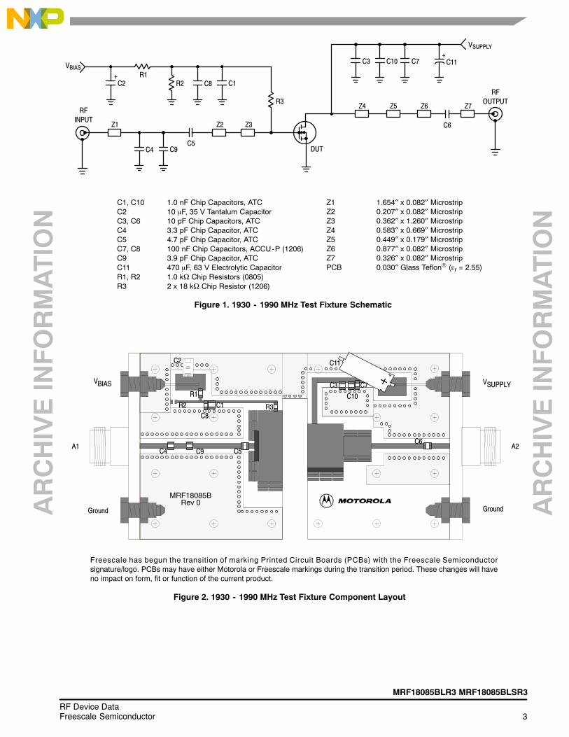
Z1 1.654″ x 0.082″ MicrostripZ2 0.207″ x 0.082″ MicrostripZ3 0.362″ x 1.260″ MicrostripZ4 0.583″ x 0.669″ MicrostripZ5 0.449″ x 0.179″ MicrostripZ6 0.877″ x 0.082″ MicrostripZ7 0.326″ x 0.082″ MicrostripPCB 0.030″ Glass Teflon® (�r = 2.55)
Figure 1. 1930 - 1990 MHz Test Fixture Schematic
Figure 2. 1930 - 1990 MHz Test Fixture Component Layout
Ground Ground
A1 A2
C11
MRF18085B
VBIAS VSUPPLY
C2
R1
R2 C1 R3C8
C9C4 C5
C3 C7
C10
C6
RF
INPUT
RF
OUTPUT
Z1
C5
C6
C8
Z3
DUT
Z5 Z6 Z7
C1
R3
C11C10+
Z2
R1C2
C7
VSUPPLY
R2+
C4 C9
Z4
C3
Rev 0
Freescale has begun the transition of marking Printed Circuit Boards (PCBs) with the Freescale Semiconductorsignature/logo. PCBs may have either Motorola or Freescale markings during the transition period. These changes will haveno impact on form, fit or function of the current product.
Freescale has begun the transition of marking Printed Circuit Boards (PCBs) with the Freescale Semiconductorsignature/logo. PCBs may have either Motorola or Freescale markings during the transition period. These changes will haveno impact on form, fit or function of the current product.
AR
CH
IVE
INF
OR
MA
TIO
N
AR
CH
IVE
INF
OR
MA
TIO
N
6RF Device Data
Freescale Semiconductor
MRF18085BLR3 MRF18085BLSR3
TYPICAL CHARACTERISTICS(Performed on a GSM EDGE Optimized Demo Board)
Figure 5. Power Gain versus Output Power
Pout, OUTPUT POWER (WATTS)
10
Figure 6. Error Vector Magnitude versusFrequency
0
f, FREQUENCY (GHz)
5
1.5
Gps
, PO
WE
R G
AIN
(dB
)
1.91
EV
M,
ER
RO
R V
EC
TO
R M
AG
NIT
UD
E (
%)
Figure 7. Power Gain versus Output Power
14
Pout, OUTPUT POWER (WATTS)
9
Figure 8. EVM and Gain versus Output Power
Pout, OUTPUT POWER (dBm) AVG.
1
0 34 36
6
10
0.5
100
2.5
1.981.95
11
η,
DR
AIN
EF
FIC
IEN
CY
(%
)
020
Figure 9. Power Gain and IRLversus Frequency
14
f, FREQUENCY (GHz)
111.85
13.5
2.051.951.90 2.00
10
13
14
1.97
40 38 50
14
13
11
9
8
11
12
1.94 1.96
3.5
60 80
12
13
3
2
4
5
10
Gps
, PO
WE
R G
AIN
(dB
)
−30
−15
−25
−20
−5
−10
12
11.5
1 1.93 1.991.92
4.5
100
2
1
3
4
2.0
Figure 10. Power Gain and Efficiencyversus Output Power
16
Pout, OUTPUT POWER (WATTS)
10
14
101 100
Gps
, PO
WE
R G
AIN
(dB
)
60
30
10
0
20
50
40
12
EV
M,
ER
RO
R V
EC
TO
R M
AG
NIT
UD
E (
%)
Gps
, PO
WE
R G
AIN
(dB
)
42 44 46 48
15
13
11
12.5
13
VDD = 26 Vdc
f = 1960 MHz
600 mA
400 mA
800 mA
IDQ = 1000 mA
Pout = 38 W Avg.
28 W Avg.
19 W Avg.
VDD = 26 Vdc
IDQ = 800 mA
24 V
VDD = 20 V
32 V
28 V
Gps
EVM
VDD = 26 Vdc
IDQ = 800 mA
30 W
30 W80 W
80 W
�
Gps
9.5
10.5
11.5
12.5
13.5
Gps
, PO
WE
R G
AIN
(dB
)
40
12
−35
VDD = 26 Vdc
IDQ = 800 mA
f = 1960 MHz
AR
CH
IVE
INF
OR
MA
TIO
N
AR
CH
IVE
INF
OR
MA
TIO
N
MRF18085BLR3 MRF18085BLSR3
7RF Device DataFreescale Semiconductor
GSM TEST SIGNAL
Figure 11. EDGE Spectrum
−10
−20
−30
−40
−50
−60
−70
−80
−90
−100
200 kHz Span 2 MHzCenter 1.96 GHz
−110
400 kHz
600 kHz
400 kHz
600 kHz
(dB
)
Reference Power VBW = 30 kHz
Sweep Time = 70 ms
RBW = 30 kHz
AR
CH
IVE
INF
OR
MA
TIO
N
AR
CH
IVE
INF
OR
MA
TIO
N
8RF Device Data
Freescale Semiconductor
MRF18085BLR3 MRF18085BLSR3
Figure 12. Series Equivalent Source and Load Impedance
fMHz
ZsourceΩ
ZloadΩ
1805
1880
1.43 - j3.74
1.5 - j4.13
1.27 - j3.95
2 - j3.60
1.98 - j3.57
2.13 - j3.16
VDD = 26 V, IDQ = 800 mA, Pout = 85 W CW
Zo = 5 Ω
f = 1990 MHz
f = 1990 MHz
f = 1805 MHz
f = 1805 MHz
1930
1990 1.86 - j4.76 2.17 - j3.36
Zload
Zsource
Zsource = Test circuit impedance as measured from gate to ground.
Zload = Test circuit impedance as measured from drain to ground.
Zsource
Zload
Input
Matching
Network
Device
Under Test
Output
Matching
Network
AR
CH
IVE
INF
OR
MA
TIO
N
AR
CH
IVE
INF
OR
MA
TIO
N
MRF18085BLR3 MRF18085BLSR3
9RF Device DataFreescale Semiconductor
NOTES
AR
CH
IVE
INF
OR
MA
TIO
N
AR
CH
IVE
INF
OR
MA
TIO
N
10RF Device Data
Freescale Semiconductor
MRF18085BLR3 MRF18085BLSR3
NOTES
AR
CH
IVE
INF
OR
MA
TIO
N
AR
CH
IVE
INF
OR
MA
TIO
N
MRF18085BLR3 MRF18085BLSR3
11RF Device DataFreescale Semiconductor
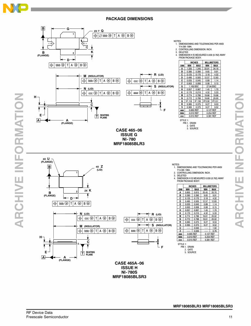
PACKAGE DIMENSIONS
CASE 465-06ISSUE GNI-780
MRF18085BLR3
NOTES:1. DIMENSIONING AND TOLERANCING PER ANSI
Y14.5M−1994.2. CONTROLLING DIMENSION: INCH.3. DELETED4. DIMENSION H IS MEASURED 0.030 (0.762) AWAY
FROM PACKAGE BODY.
DIM MIN MAX MIN MAX
MILLIMETERSINCHES
A 1.335 1.345 33.91 34.16
B 0.380 0.390 9.65 9.91
C 0.125 0.170 3.18 4.32
D 0.495 0.505 12.57 12.83
E 0.035 0.045 0.89 1.14
F 0.003 0.006 0.08 0.15
G 1.100 BSC 27.94 BSC
H 0.057 0.067 1.45 1.70
K 0.170 0.210 4.32 5.33
N 0.772 0.788 19.60 20.00
Q .118 .138 3.00 3.51
R 0.365 0.375 9.27 9.53
STYLE 1:PIN 1. DRAIN
2. GATE 3. SOURCE
1
3
2
D
G
K
C
E
H
S
FS 0.365 0.375 9.27 9.52
M 0.774 0.786 19.66 19.96
aaa 0.005 REF 0.127 REF
bbb 0.010 REF 0.254 REF
ccc 0.015 REF 0.381 REF
Q2X
MAMbbb B MT
MAMbbb B MT
B
B(FLANGE)
SEATING
PLANE
MAMccc B MT
MAMbbb B MT
A A(FLANGE)
T
N (LID)
M (INSULATOR)
MAMaaa B MT
(INSULATOR)
R
MAMccc B MT
(LID)
CASE 465A-06ISSUE HNI-780S
MRF18085BLSR3
NOTES:1. DIMENSIONING AND TOLERANCING PER ANSI
Y14.5M−1994.2. CONTROLLING DIMENSION: INCH.3. DELETED4. DIMENSION H IS MEASURED 0.030 (0.762) AWAY
FROM PACKAGE BODY.
DIM MIN MAX MIN MAX
MILLIMETERSINCHES
A 0.805 0.815 20.45 20.70
B 0.380 0.390 9.65 9.91
C 0.125 0.170 3.18 4.32
D 0.495 0.505 12.57 12.83
E 0.035 0.045 0.89 1.14
F 0.003 0.006 0.08 0.15
H 0.057 0.067 1.45 1.70
K 0.170 0.210 4.32 5.33
M 0.774 0.786 19.61 20.02
R 0.365 0.375 9.27 9.53
STYLE 1:PIN 1. DRAIN
2. GATE5. SOURCE
C
E
H
F3
bbb 0.010 REF 0.254 REF
ccc 0.015 REF 0.381 REF
aaa 0.005 REF 0.127 REF
S 0.365 0.375 9.27 9.52
N 0.772 0.788 19.61 20.02
U −−− 0.040 −−− 1.02
Z −−− 0.030 −−− 0.76
SEATING
PLANE
MAMccc B MT
MAMbbb B MT
A A(FLANGE)
T
N (LID)
M (INSULATOR)
MAMccc B MT
MAMaaa B MT
R (LID)
S (INSULATOR)
1
2
D
K
U(FLANGE)
4X
Z(LID)
4X
MAMbbb B MT
B
B(FLANGE)
2X
AR
CH
IVE
INF
OR
MA
TIO
N
AR
CH
IVE
INF
OR
MA
TIO
N
12RF Device Data
Freescale Semiconductor
MRF18085BLR3 MRF18085BLSR3
Information in this document is provided solely to enable system and softwareimplementers to use Freescale Semiconductor products. There are no express orimplied copyright licenses granted hereunder to design or fabricate any integratedcircuits or integrated circuits based on the information in this document.
Freescale Semiconductor reserves the right to make changes without further notice toany products herein. Freescale Semiconductor makes no warranty, representation orguarantee regarding the suitability of its products for any particular purpose, nor doesFreescale Semiconductor assume any liability arising out of the application or use ofany product or circuit, and specifically disclaims any and all liability, including withoutlimitation consequential or incidental damages. �Typical� parameters that may beprovided in Freescale Semiconductor data sheets and/or specifications can and dovary in different applications and actual performance may vary over time. All operatingparameters, including �Typicals�, must be validated for each customer application bycustomer�s technical experts. Freescale Semiconductor does not convey any licenseunder its patent rights nor the rights of others. Freescale Semiconductor products arenot designed, intended, or authorized for use as components in systems intended forsurgical implant into the body, or other applications intended to support or sustain life,or for any other application in which the failure of the Freescale Semiconductor productcould create a situation where personal injury or death may occur. Should Buyerpurchase or use Freescale Semiconductor products for any such unintended orunauthorized application, Buyer shall indemnify and hold Freescale Semiconductorand its officers, employees, subsidiaries, affiliates, and distributors harmless against allclaims, costs, damages, and expenses, and reasonable attorney fees arising out of,directly or indirectly, any claim of personal injury or death associated with suchunintended or unauthorized use, even if such claim alleges that FreescaleSemiconductor was negligent regarding the design or manufacture of the part.
USA/Europe or Locations Not Listed:Freescale SemiconductorTechnical Information Center, CH3701300 N. Alma School RoadChandler, Arizona 85224+1-800-521-6274 or [email protected]
Japan:Freescale Semiconductor Japan Ltd.Technical Information Center3-20-1, Minami-Azabu, Minato-kuTokyo 106-0047, Japan0120 191014 or +81 3 3440 [email protected]
Asia/Pacific:Freescale Semiconductor Hong Kong Ltd.Technical Information Center2 Dai King StreetTai Po Industrial EstateTai Po, N.T., Hong Kong+800 2666 [email protected]
For Literature Requests Only:Freescale Semiconductor Literature Distribution CenterP.O. Box 5405Denver, Colorado 802171-800-441-2447 or 303-675-2140Fax: [email protected]