RF Power Field Effect TransistorsN--Channel Enhancement--Mode Lateral MOSFETsDesigned for W--CDMA base station applications with frequencies from 2110
to 2170 MHz. Suitable for TDMA, CDMA and multicarrier amplifier applications.To be used in Class AB for PCN--PCS/cellular radio and WLL applications.
• Typical 2--Carrier W--CDMA Performance: VDD = 28 Volts, IDQ = 500 mA,Pout = 10 Watts Avg., f = 2112.5 MHz, Channel Bandwidth = 3.84 MHz,PAR = 8.5 dB @ 0.01% Probability on CCDF.Power Gain 14.5 dBDrain Efficiency 25.5%IM3 @ 10 MHz Offset --37 dBc in 3.84 MHz Channel BandwidthACPR @ 5 MHz Offset --39 dBc in 3.84 MHz Channel Bandwidth
• Capable of Handling 5:1 VSWR, @ 28 Vdc, 2140 MHz, 45 Watts CWOutput Power
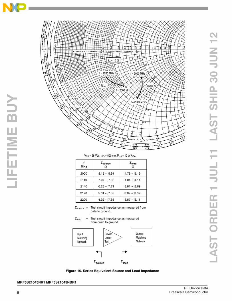
Features• Characterized with Series Equivalent Large--Signal Impedance Parameters
• Internally Matched for Ease of Use• Qualified Up to a Maximum of 32 VDD Operation• Integrated ESD Protection• 200°C Capable Plastic Package• N Suffix Indicates Lead--Free Terminations. RoHS Compliant.• In Tape and Reel. R1 Suffix = 500 Units per 44 mm, 13 inch Reel.
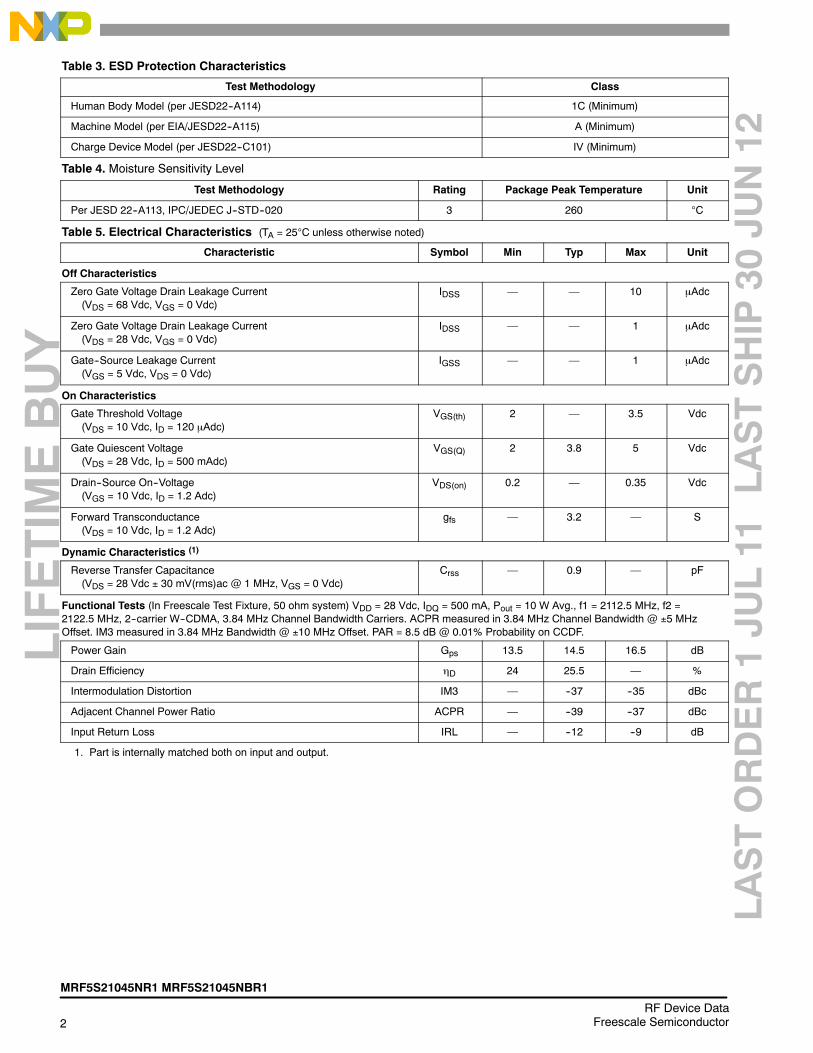
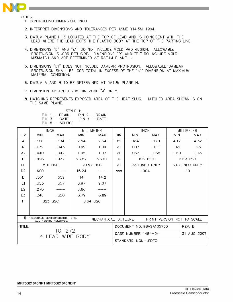
Table 1. Maximum Ratings
Rating Symbol Value Unit
Drain--Source Voltage VDSS --0.5, +68 Vdc
Gate--Source Voltage VGS --0.5, +15 Vdc
Total Device Dissipation @ TC = 25°CDerate above 25°C
PD 1300.74
WW/°C
Storage Temperature Range Tstg -- 65 to +150 °C
Operating Junction Temperature TJ 200 °C
Table 2. Thermal Characteristics
Characteristic Symbol Value (1,2) Unit
Thermal Resistance, Junction to CaseCase Temperature 80°C, 45 W CWCase Temperature 79°C, 10 W CW
RθJC1.351.48
°C/W
1. MTTF calculator available at http://www.freescale.com/rf. Select Software & Tools/Development Tools/Calculators to access MTTFcalculators by product.
2. Refer to AN1955, Thermal Measurement Methodology of RF Power Amplifiers. Go to http://www.freescale.com/rf.Select Documentation/Application Notes -- AN1955.
Figure 1. MRF5S21045NR1(NBR1) Test Circuit Schematic
Z7 0.500″ x 1.000″ MicrostripZ8, Z13 0.270″ x 0.080″ MicrostripZ10 0.789″ x 0.080″ MicrostripZ11 0.527″ x 0.080″ MicrostripZ12 0.179″ x 0.080″ MicrostripPCB Taconic TLX8--0300, 0.030″, εr = 2.55
Z1, Z9 0.250″ x 0.080″ MicrostripZ2 0.987″ x 0.080″ MicrostripZ3 0.157″ x 0.080″ MicrostripZ4 0.375″ x 0.080″ MicrostripZ5 0.480″ x 1.000″ MicrostripZ6 0.510″ x 0.080″ Microstrip
C2C1R2
VBIASVSUPPLY
C6C5C4
C8 C9 C10
C3
C13
C7
RFOUTPUT
RFINPUT
R1
Z1 Z2 Z3 Z4 Z5
Z6
Z13
Z8
Z7 Z12 Z11 Z9
+
DUT
R3
C11
Z10
C12
C15C14
Table 6. MRF5S21045NR1(NBR1) Test Circuit Component Designations and ValuesPart Description Part Number Manufacturer
Figure 12. MTTF Factor versus Junction Temperature
This above graph displays calculated MTTF in hours x ampere2
drain current. Life tests at elevated temperatures have correlated tobetter than ±10% of the theoretical prediction for metal failure. DivideMTTF factor by ID2 for MTTF in a particular application.
108
107
106
110 130 160 180 200
MTTFFACTOR(HOURSxAM
PS2 )
100 120 140 150 170 190
W--CDMA TEST SIGNAL
100.0001
100
0
PEAK--TO--AVERAGE (dB)
Figure 13. CCDF W--CDMA 3GPP, Test Model 1,64 DPCH, 67% Clipping, Single--Carrier Test Signal
10
1
0.1
0.01
0.001
2 4 6 8
Figure 14. 2-Carrier W-CDMA Spectrum
f, FREQUENCY (MHz)
3.84 MHzChannel BW
--IM3 in3.84 MHz BW
+IM3 in3.84 MHz BW
--ACPR in3.84 MHz BW
+ACPR in3.84 MHz BW
PROBABILITY
(%)
(dB)
+20
+30
0
--10
--40
--50
--60
--70
--80
--20
205 15100--5--10--15--20--25 25
--30W--CDMA. ACPR Measured in 3.84 MHz ChannelBandwidth @±5 MHz Offset. IM3 Measured in3.84 MHz Bandwidth @±10 MHz Offset. PAR =8.5 dB @ 0.01% Probability on CCDF
Refer to the following documents to aid your design process.
Application Notes• AN1907: Solder Reflow Attach Method for High Power RF Devices in Plastic Packages
• AN1955: Thermal Measurement Methodology of RF Power Amplifiers
• AN3263: Bolt Down Mounting Method for High Power RF Transistors and RFICs in Over--Molded Plastic Packages
Engineering Bulletins• EB212: Using Data Sheet Impedances for RF LDMOS Devices
REVISION HISTORY
The following table summarizes revisions to this document.
Revision Date Description
4 Oct. 2008 • Modified data sheet to reflect RF Test Reduction described in Product and Process Change Notificationnumber, PCN12779, p. 1, 2
• Updated Part Numbers in Table 6, Component Designations and Values, to latest RoHS compliant partnumbers, p. 3
• Replaced Case Outline 1486--03, Issue C, with 1486--03, Issue D, p. 9--11. Added pin numbers 1 through 4on Sheet 1.
• Replaced Case Outline 1484--04, Issue D, with 1484--04, Issue E, p. 12--14. Added pin numbers 1 through4 on Sheet 1, replacing Gate and Drain notations with Pin 1 and Pin 2 designations.
• Added Product Documentation and Revision History, p. 15
4.1 Dec. 2009 • Corrected data sheet to reflect RF Test Reduction frequency described in Product and Process ChangeNotification number, PCN12779, p. 2
Information in this document is provided solely to enable system and softwareimplementers to use Freescale Semiconductor products. There are no express orimplied copyright licenses granted hereunder to design or fabricate any integratedcircuits or integrated circuits based on the information in this document.
Freescale Semiconductor reserves the right to make changes without further notice toany products herein. Freescale Semiconductor makes no warranty, representation orguarantee regarding the suitability of its products for any particular purpose, nor doesFreescale Semiconductor assume any liability arising out of the application or use ofany product or circuit, and specifically disclaims any and all liability, including withoutlimitation consequential or incidental damages. Typical parameters that may beprovided in Freescale Semiconductor data sheets and/or specifications can and dovary in different applications and actual performance may vary over time. All operatingparameters, including Typicals, must be validated for each customer application bycustomers technical experts. Freescale Semiconductor does not convey any licenseunder its patent rights nor the rights of others. Freescale Semiconductor products arenot designed, intended, or authorized for use as components in systems intended forsurgical implant into the body, or other applications intended to support or sustain life,or for any other application in which the failure of the Freescale Semiconductor productcould create a situation where personal injury or death may occur. Should Buyerpurchase or use Freescale Semiconductor products for any such unintended orunauthorized application, Buyer shall indemnify and hold Freescale Semiconductorand its officers, employees, subsidiaries, affiliates, and distributors harmless against allclaims, costs, damages, and expenses, and reasonable attorney fees arising out of,directly or indirectly, any claim of personal injury or death associated with suchunintended or unauthorized use, even if such claim alleges that FreescaleSemiconductor was negligent regarding the design or manufacture of the part.
USA/Europe or Locations Not Listed:Freescale Semiconductor, Inc.Technical Information Center, EL5162100 East Elliot RoadTempe, Arizona 852841--800--521--6274 or +1--480--768--2130www.freescale.com/support
Europe, Middle East, and Africa:Freescale Halbleiter Deutschland GmbHTechnical Information CenterSchatzbogen 781829 Muenchen, Germany+44 1296 380 456 (English)+46 8 52200080 (English)+49 89 92103 559 (German)+33 1 69 35 48 48 (French)www.freescale.com/support
Japan:Freescale Semiconductor Japan Ltd.HeadquartersARCO Tower 15F1--8--1, Shimo--Meguro, Meguro--ku,Tokyo 153--0064Japan0120 191014 or +81 3 5437 [email protected]
Asia/Pacific:Freescale Semiconductor China Ltd.Exchange Building 23FNo. 118 Jianguo RoadChaoyang DistrictBeijing 100022China+86 10 5879 [email protected]
For Literature Requests Only:Freescale Semiconductor Literature Distribution Center1--800--441--2447 or +1--303--675--2140Fax: [email protected]
Document Number: MRF5S21045NRev. 4.1, 12/2009
RoHS--compliant and/or Pb--free versions of Freescale products have the functionality and electricalcharacteristics of their non--RoHS--compliant and/or non--Pb--free counterparts. For furtherinformation, see http://www.freescale.com or contact your Freescale sales representative.
For information on Freescales Environmental Products program, go to http://www.freescale.com/epp.