FRISC-E: A 250-MIPS Hybrid Microprocessor by H.J. Grueb, J.E McDonald, and T Creedon A 32-bit RISC design with advanced differential bipolar logic mplementing the principles of Reduced Instruction Set Computers (RISC) with advanced high-speed circuit technolo- gy is both attractive and difficult. Ad- vanced bipolar circuit technology, for instance, offers gate delays as low as 55 ps but dissipates considerable power. There- fore, a high-speed microprocessor fabricat- ed with this technology must be partitioned into LSI circuits to increase yield and reduce heat flux. But partitioning requires die-to-die interconnections, which cause signal propagation delays. The FRISC series of Fast Reduced Instruction Set Computer designs goes a long way towards solving these problems. The FRISC design adapts many concepts of the Berkeley RISC [1,2] and Stanford MIPS [3] single-chip CMOS microproces- sors to advanced high-speed circuit tech- nology. Although high speed circuit tech- nologies like GaAs or Advanced Bipolar offer very low gate-propagation delays, their yield and power-dissipation problems force would-be developers to consider new design and implementation strategies [4,- 5hI. For FRISC-E-the most ambitious ver- sion to date-the targeted instruction rate of 250 MIPS led us to a seven-stage in- struction pipeline. We partitioned the pro- cessor into 11 chips, not only because of Advanced Bipolar's high power dissipation, but also because its process yield does not support VLSI fabrication. This partitioning severely compromises the performance of printed-circuit-board implementations of the processor because of the long intercon- nect paths between dies. Fortunately, it is possible to design systems with "flow-thro- ugh architectures," which use die-to-die I/O pipelining and can be partitioned without significantly reducing performance. But these designs must be implemented under stringent limitations. The interconnections between dies are implemented as transmission lines with a polyimide dielectric (e, = 3.1). An electri- cal signal propagates along such a line at a velocity of only 17 cdns, so a sequential system built around such transmission lines must be made smaller if the cycle times are to become shorter. One might be tem- pted to seek relief by designing the die interconnects as something other than transmission lines. but that would make 16 8755-3996/90/0500-0016$1.00 0 1990 IEEE Circuits and Devices ___ ~~ ~ --
Transcript
FRISC-E: A 250-MIPS Hybrid Microprocessor by H.J. Grueb, J.E McDonald, and T Creedon
A 32-bit RISC design with advanced differential bipolar logic
mplementing the principles of Reduced Instruction Set Computers (RISC) with advanced high-speed circuit technolo- gy is both attractive and difficult. Ad- vanced bipolar circuit technology, for instance, offers gate delays as low as 55 ps but dissipates considerable power. There- fore, a high-speed microprocessor fabricat- ed with this technology must be partitioned into LSI circuits to increase yield and reduce heat flux. But partitioning requires die-to-die interconnections, which cause signal propagation delays. The FRISC series of Fast Reduced Instruction Set Computer designs goes a long way towards solving these problems.
The FRISC design adapts many concepts of the Berkeley RISC [1,2] and Stanford MIPS [3] single-chip CMOS microproces- sors to advanced high-speed circuit tech- nology. Although high speed circuit tech- nologies like GaAs or Advanced Bipolar offer very low gate-propagation delays, their yield and power-dissipation problems force would-be developers to consider new design and implementation strategies [4,- 5hI.
For FRISC-E-the most ambitious ver-
sion to date-the targeted instruction rate of 250 MIPS led us to a seven-stage in- struction pipeline. We partitioned the pro- cessor into 1 1 chips, not only because of Advanced Bipolar's high power dissipation, but also because its process yield does not support VLSI fabrication. This partitioning severely compromises the performance of printed-circuit-board implementations of the processor because of the long intercon- nect paths between dies. Fortunately, it is possible to design systems with "flow-thro- ugh architectures," which use die-to-die I/O pipelining and can be partitioned without significantly reducing performance. But these designs must be implemented under stringent limitations.
The interconnections between dies are implemented as transmission lines with a polyimide dielectric (e, = 3.1). An electri- cal signal propagates along such a line at a velocity of only 17 c d n s , so a sequential system built around such transmission lines must be made smaller if the cycle times are to become shorter. One might be tem- pted to seek relief by designing the die interconnects as something other than transmission lines. but that would make
16 8755-3996/90/0500-0016$1.00 0 1990 IEEE Circuits and Devices
___ ~~ ~ --
things worse: transmission-line characteris- tics avoid the slow RC charging otherwise observed on long die interconnects.
As always, the transmission lines must have constant impedance and line termina- tion to avoid signal reflections. The charac- teristic impedance of these transmission lines is usually 50 ohms. Such low-impeda- nce transmission lines require robust I/O drivers that can deliver high output currents -16 mA is needed to generate the 800 - -mV logic swing required for ECL.
All of this effort to implement Advanced Bipolar circuitry is justified by the technol- ogy’s combination of low gate propagation delays-in the same range as 1-pm GaAs MESFET gates-and high-current drive capability.
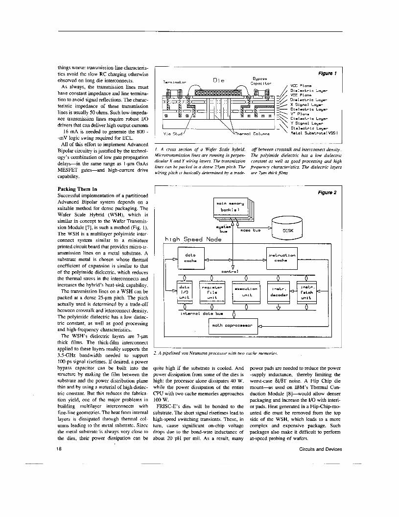
Packing Them In Successful implementation of a partitioned Advanced Bipolar system depends on a suitable method for dense packaging. The Wafer Scale Hybrid (WSH), which is similar in concept to the Wafer Transmis- sion Module [7], is such a method (Fig. 1). The WSH is a multilayer polyimide inter- connect system similar to a miniature printed circuit board that provides micro-tr- ansmission lines on a metal substrate. A substrate metal is chosen whose thermal coefficient of expansion is similar to that of the polyimide dielectric, which reduces the thermal stress in the interconnects and increases the hybrid’s heat-sink capability.
The transmission lines on a WSH can be packed at a dense 25-pm pitch. The pitch actually used is determined by a trade-off between crosstalk and interconnect density. The polyimide dielectric has a low dielec- tric constant, as well as good processing and high-frequency characteristics.
The WSH’s dielectric layers are 7-pm thick films. The thick-film interconnect applied to these layers readily supports the 3.5-GHz bandwidth needed to support 100-ps signal risetimes. If desired, a power bypass capacitor can be built into the structure by making the film between the substrate and the power distribution plane thin and by using a material of high dielec- tric constant. But this reduces the fabrica- tion yield, one of the major problems in building multilayer interconnects with fine-line geometries. The heat from internal layers is dissipated through thermal col- umns leading to the metal substrate. Since the metal substrate i s always very close to the dies, their power dissipation can be
18
Figure 1 BLJpase
/ VCC Plane Capac 1 tar Termlnotar Die
n Dielectric Layer VEE Plane Olelectrlc Layer X Slpnol Layor Dtelectrlc Layer VT Plone Dlelectrfc Louer
I . A cross section of a Wafer Scale hybrid. Microtransmission lines are running in perpen- dicular X and Y wiring layers. The transmission lines can be packed in a dense 25pm pitch. The wiring pitch is basically determined by a trade-
off between crosstalk and interconnect density, The polyimide dielectric has a low dielectric constant as well as good processing and high frequency characteristics. The dielectric layers are 7pm thick films.
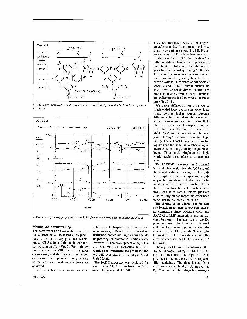
Figure 2
lnsLrucLlon
2. A pipelined von Neumann processor with two cache memories
quite high if the substrate is cooled. And power dissipation from some of the dies is high: the processor alone dissipates 40 W, while the power dissipation of the entire CPU with two cache memories approaches 100 w.
FRISC-E’s dies will be bonded to the substrate. The short signal risetimes lead to high-speed switching transients. These, in turn, cause significant on-chip voltage drops due to the bond-wire inductance of about 20 pH per mil. As a result, many
power pads are needed to reduce the power -supply inductance, thereby limiting the worst-case 6I/6T noise. A Flip Chip die mount-as used on IBM’s Thermal Con- duction Module [8]-would .allow denser packaging and increase the I/O with interi- or pads. Heat generated in a Flip-Chip-mo- unted die must be removed from the top side of the WSH, which leads to a more complex and expensive package. Such packages also make it difficult to perform at-speed probing of wafers.
Circuits and Devices
Figure 3
input offset 1 eve 1
level 1
level2 B B
level3 A - K X A YVEE = - 5 V YVEE = - 5v
3. The carry propagation gate used on the critical ALU path and a latch with an asynchro- nous clear.
4 . The delays of a carry propagate gate with the fanout encountered on the critical ALU path
Making von Neumann Hop The performance of a sequential von Neu- mann processor can be increased by pipeli- ning, which (in a fully pipelined system) lets all CPU units and the math coproces- sor work in parallel (Fig. 2). For optimum performance, the CPU units, the math coprocessor, and the data and instruction caches must be implemented very densely so that very short system-cycle times are achieved.
FRISC-E's two cache memories must
May 1990
isolate the high-speed CPU from slow main memory. Direct-mapped 32K-byte instruction caches are large enough to do the job; they can produce miss ratios below 1 percent [9]. The development of high-den- sity 64K-bit ECL memories [lo] will permit us to implement the processor and two 64K-byte caches on a single Wafer Scale Hybrid.
The FRISC processor was designed for npn silicon bipolar transistors with a transit frequency of 15 GHz.
They are fabricated with a self-aligned polysilicon emitter-base process and have I-pm-wide emitter stripes [ I l , 121. Propa- gation delays of 55 ps have been measured in ring oscillators. RPI has designed a differential-logic family for implementing the FRISC architecture. The differential gates have a low voltage swing (250 mV). They can implement any boolean function with three inputs by using three levels of current switches with wired or collectors at levels 2 and 3. ECL output buffers are used to reduce sensitivity to loading. The propagation delay from a level 1 input to the buffer output is 80 ps with a fanout of one (Figs 3, 4).
We chose differential logic instead of single-ended logic because its lower logic swing permits higher speeds. Because differential logic is inherently power bal- anced, its switching noise is very small. In FRISC-E, even the high-speed internal CPU bus is differential to reduce the 6Y6T noise in the system and to save power through the low differential logic swing. These benefits justify differential logic's need for twice the number of signal interconnections required by single-ended logic. Three-level, single-ended logic would require three reference voltages per gate.
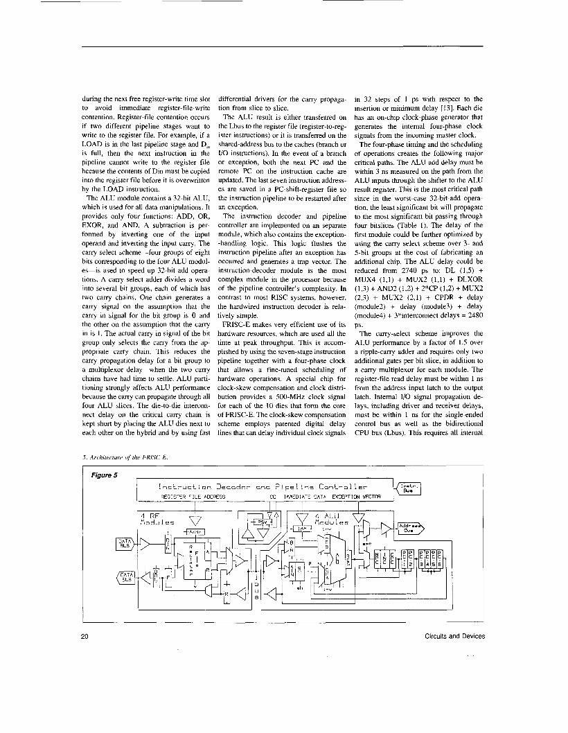
The FRISC-E processor has 3 external buses: the instruction bus, the 1/0 bus, and the shared address bus (Fig. 5). The data bus is split into a data input and a data output bus to obtain a faster data cache interface. All addresses are transferred over the shared address bus to the cache memo- ries. Because it uses a remote program counter, only branch target addresses need to be Sent to the instruction cache.
The sharing of the address bus for data and branch target address transfers causes no contention since LOAD/STORE and BRANCH/JUMP instructions use the ad- dress bus only when they are in the D1 pipeline stage. The Lbus is an internal CPU bus for transferring data between the register file, the ALU, and the Status regis- ter module, and for interfacing with the math coprocessor. All CPU buses are 32 bits wide.
The register file module contains a 30 -by-32-bit single-port register file [13]. The operand fetch from the register file is pipelined to increase the effective register- -file bandwidth. The data loaded from memory is saved in the holding register D,. The data is only written into memory
19
during the next free register-write time slot to avoid immediate register-file-write contention. Register-file contention occurs if two different pipeline stages want to write to the register file. For example, if a LOAD is in the last pipeline stage and D, is full, then the next instruction in the pipeline cannot write to the register file because the contents of Din must be copied into the register file before it is overwritten by the LOAD instruction.
The ALU module contains a 32-bit ALU, which is used for all data manipulations. It provides only four functions: ADD, OR, EXOR, and AND. A subtraction is per- formed by inverting one of the input operand and inverting the input carry. The carry-select scheme-four groups of eight bits corresponding to the four ALU modul- es-is used to speed up 32-bit add opera- tions. A carry-select adder divides a word into several bit groups, each of which has two carry chains. One chain generates a carry signal on the assumption that the carry in signal for the bit group is 0 and the other on the assumption that the carry in is 1 . The actual carry in signal of the bit group only selects the carry from the ap- propriate carry chain. This reduces the carry propagation delay for a bit group to a multiplexor delay when the two carry chains have had time to settle. ALU parti- tioning strongly affects ALU performance because the carry can propagate through all four ALU slices. The die-to-die intercon- nect delay on the critical carry chain is kept short by placing the ALU dies next to each other on the hybrid and by using fast
W
5 . Architecture of the FRISC-E.
I I I
differential drivers for the carry propaga- tion from slice to slice.
The ALU result is either transferred on the Lbus to the register file (register-to-reg- ister instructions) or it is transferred on the shared-address bus to the caches (branch or I/O instructions). In the event of a branch or exception, both the next PC and the remote PC on the instruction cache are updated. The last seven instruction address- es are saved in a PC-shift-register file so the instruction pipeline to be restarted after an exception.
The instruction decoder and pipeline controller are implemented on an separate module, which also contains the exception- -handling logic. This logic flushes the instruction pipeline after an exception has occurred and generates a trap vector. The instruction-decoder module is the most complex module in the processor because of the pipeline controller’s complexity. In contrast to most RISC systems, however, the hardwired instruction decoder is rela- tively simple.
FRISC-E makes very efficient use of its hardware resources, which are used all the time at peak throughput. This is accom- plished by using the seven-stage instruction pipeline together with a four-phase clock that allows a fine-tuned scheduling of hardware operations. A special chip for clock-skew compensation and clock distri- bution provides a 500-MHz clock signal for each of the 10 dies that form the core of FRISC-E. The clock-skew compensation scheme employs patented digital delay lines that can delay individual clock signals
in 32 steps of 1 ps with respect to the insertion or minimum delay [13]. Each die has an on-chip clock-phase generator that generates the internal four-phase clock signals from the incoming master clock.
The four-phase timing and the scheduling of operations creates the following major critical paths. The ALU add delay must be within 3 ns measured on the path from the ALU inputs through the shifter to the ALU result register. This is the most critical path since in the worst-case 32-bit-add opera- tion, the least significant bit will propagate to the most significant bit passing through four bitslices (Table 1) . The delay of the first module could be further optimized by using the carry select scheme over 3- and 5-bit groups at the cost of fabricating an additional chip. The ALU delay could be reduced from 2740 ps to: DL ( 1 3 ) + MUX4 (1 , l ) + MUX2 (1,l) + DLXOR (1,3)+ AND2 (1,2)+ 2*CP(1,2)+ MUX2 (2,3) + MUX2 (2,l) + CPDR + delay (module2) + delay (module3) + delay (module4) + 3*interconnect delays = 2480 PS.
The carry-select scheme improves the ALU performance by a factor of 1.5 over a ripple-carry adder and requires only two additional gates per bit slice, in addition to a carry multiplexor for each module. The register-file read delay must be within 1 ns from the address input latch to the output latch. Internal I/O signal propagation de- lays, including driver and receiver delays, must be within 1 ns for the single-ended control bus as well as the bidirectional CPU bus (Lbus). This requires all internal
Figure 5
Instruction Decoder ond Pipeline Controller REGISTER FILE ADDRESS CC IhhEDlATE DATA EXCEPTION VECTOR -
I
20 Circuits and Devices
CPU interconnections to be shorter than 12 cm.
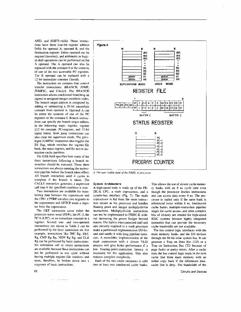
The User-Visible State The FRISC-E's 30-bit register file is
divided into two banks with two global registers (Fig. 6). The Processor Status Word (PSW) is also split in two separate registers with the exception of four global status bits. One bank and one status regis- ter are dedicated to the supervisor (kernel) mode. This allows a fast context switch to the supervisor mode if an exception occurs or if the user process executes a supervisor call. A fast context switch is desirable because many tasks are migrated from hardware to software in GaAs or Advanced Bipolar RISC systems because off-the-shelf high-speed hardware components are either expensive or unavailable [6]. The excep- tion logic sets the supervisor-mode (SM) and bank-select (BS) flags after an excep- tion, and it also switches the instruction-ca- che partition. Two instruction-cache parti- tions are provided for the supervisor pro- cess and the user process(es). Without different cache partitions the two processes will overwrite each other's cache foot- prints, causing many cache misses after a context switch.
The status register contains the following condition flags: Negative, Zero, Carry, and Overflow, the flags for the shift/rotate operation (C-1, C1, C2, C3, C4), and the Interrupt Enable (I) and Arithmetic Trap Enable (AT) flags. It also contains the Bank Select (BS) flag that indicates which register file, status register, and instruction cache partition have been selected. The Supervisor Mode flag (SM) indicates if the currently running process has supervisor privileges. The Previous Supervisor Mode (PS) flag reflects the state of the SM flag before the exception occurred. Supervisor privilege is required for switching the BS flag and for performing LOAD and STORE instructions from or to protected 1/0 space. After an exception has occurred the processor enters protected mode, which is indicated by the (PM) flag. In protected mode all asynchronous interrupts (user and coprocessor interrupts) are disabled and the last four PC registers are locked. If a trap occurs in protected mode, a system-error trap is invoked. A second interrupt or trap can not be accepted before the state of the interrupted process, including the return addresses, has been saved. Only two regis- ters in the PC shift-register file are directly
May 1990
Table I
A 0 1 r , BIT-SLICE-0 4R0 i 0 0
A l D 0 I I 0
87 R?
A 7
ALU MODULE1 C - I N
ALU Module with Carry Select Adder
Critical Path: ALU i n p u t A 1 t o su% output in ALU module 4 for a
Control Signals: (p4: SHIFT-11, F?)
Gate Definition: FUNC:F = ( SANI)* (A*i j ) t SXOR*(A xor B) )
Gate Delay Model: Delay(input-level, fanout) -
SHIFT right by 1 ar.d 32 bit add operation.
(PI : INVA, INV3, S3-1, SADD=l, SXOR-1, SAYD=O, C I N ) ;
accessible: the one required for branch calculations and the one that contains the address for restarting after an exception. The last four instruction addresses on the PC-register stack can be read by a se- quence of GET LPC instructions.
FRISC-E has a regular instruction set with typical RISC features (Table 2) [2,14- 151. Only LOAD and STORE instructions are provided for accessing memory. The following memory addressing modes are supported: Register, Register+lndex, Reg- ister f12 bit displacement, and PC Rela- tive. An absolute addressing mode with a positive or negative 12-bit address is also possible. FRISC-E recognizes data depen- dencies after LOAD instructions. If one of
the three instructions following the LOAD references the register to be loaded, the system will not execute this dependent instruction until the LOAD instruction is completed. This avoids the scheduling of NOOP instructions to prevent pipeline hazards. Consecutive LOAD instructions can be executed without a delay penalty if they reference different cache banks. LOA- DLOAD and LOAD/STORE sequences that reference the same cache bank incur a delay of one cycle. STORE/STORE and STORELOAD sequence that accesses the same cache bank incur a delay of two cycles.
The instruction set contains five integer manipulation instructions: ADD, OR, XOR,
21
AND, and SHIFT+ADD. These instruc- tions have three four-bit register address fields for operand A, operand B, and the destination register. Either operand can be negated (inverted), and arithmetic or logic- al-shift operations can be performed on the A operand. The A operand can also be replaced with the constant 0 or the contents of one of the two accessible PC registers. The B operand can be replaced with a 12-bit immediate constant (literal).
The instruction set contains four control transfer instructions: BRANCH, JUMP, JUMPSC, and CALLS. The BRANCH instruction allows conditional branching on signed or unsigned integer condition codes. The branch target address is computed by adding or subtracting a 20-bit immediate constant from operand A. Operand A can be either the contents of one of the PC registers or the constant 0. Branch instruc- tions can specify the branch target address in the following ways: register, register f 1 2 bit constant, PC+register, and 12-bit signal literal. Both jump instructions can also clear the supervisor mode. The privi- leged JUMPSC instruction also toggles the BS flag, which switches the register-file bank, the status register, and the active-ins- truction-cache partition.
The EXE field specifies how many of the three instructions following a branch in- struction should be executed. These three instructions are always entering the instruc- tion pipeline before the branch takes effect. All branch instruction need 4 cycles to complete if the branch is taken. The CALLS instruction generates a supervisor call trap if the specified condition is true.
Two instructions are available for trans- ferring data between the coprocessor and the CPU. CPTRF transfers two registers to the coprocessor and GETCP reads a regis- ter from the coprocessor.
The GET instruction saves either the processor status word (PSW), the PC-3, the PC-6 (LPC), or an immediate constant in a register. Several one- and two-operand instructions not shown in Table 2 can be performed by the basic instruction set. For example, instructions like INC Rg, DEC Rg, CMP Rg Rg, MOV Rg Rg, and CLR Rg can be performed by basic instructions. No subroutine call or return instructions are available because these instructions can not be performed in one cycle without having multiple register file windows and must, therefore, be broken down into a sequence of basic instructions.
22
- A T
AT
REGISTER FILE
I C-1 N 2 C W C4 C3 C2 C1
I C-1 N 2 C OV C4 C3 C2 Cl
n e
STATUS REGISTER
PROGRAM COUNTER
6 . The user visible state of the FRISC-E processor
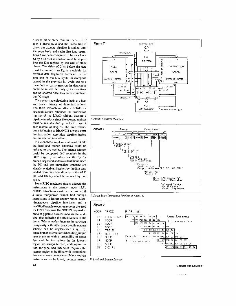
System Architecture A high-speed node is made up of the FR- ISC-E CPU, a math coprocessor, and a system-bus interface (Fig. 7). The math coprocessor is fed from the same instruc- tion stream as the processor and handles floating point and integer multiply/divide instructions. Multiply/divide instructions can not be implemented in FRISC-E with- out increasing the power budget beyond reason. The tightly interconnected shift and add circuitry required in a math processor make a partitioned implementation I/O-bo- und and saddle it with long pipeline laten- cies. A monolithic implementation of the math coprocessor with a slower VLSI process will give better performance if a low floating-point-instruction latency is necessary for the application. This also reduces compiler complexity.
Each of the two cache memories is split into at least two interleaved cache banks.
This allows the use of slower cache memo- ry banks with an 8 ns cycle time even though the processor fetches instructions and can access data every 4 ns. The pro- cessor is stalled only if the same bank is referenced twice within 8 ns. Interleaved cache banks, multiple-instruction pipeline stages for cache access, and other complex bits of trickery are needed for high-speed RISC systems because highly integrated memories that can provide the necessary cache bandwidth are not available.
The bus control logic interfaces with the main memory banks and the I/O devices through the 64-bit-wide system bus. It can generate a Trap on Data Bus (TD) or a Trap on Instruction Bus (TI) because of page faults or parity errors. After a cache miss the bus control logic reads in the next cache line from main memory with an initial copy back if the referenced data- cache line is dirty. The bandwidth of the
Circuits and Devices
main memory bus needs to be quite high- -1 Gbyte/s- in order to reduce the per- formance impact of cache misses. A four - way interleaved main memory with 32-11s access time can supply the data at full bus speed. But even with these heroic mea- sures, cache misses have a much larger performance impact on GaAs or Advanced Bipolar systems than on CMOS RISC systems [6] because of the higher ratio of main-memory-access time to cache-access time.
The instruction cache contains the remote program counter, which is incremented during register-to-register instructions and is loaded with the branch target address if a branch is taken. The branch target ad- dresses and the data I/O addresses are transferred on the shared address bus to the cache memories.
The data bus is split into an input and output bus. This avoids the use of a slow bidirectional bus to the data cache, which permits the use of slower cache memories. The FRISC architecture allows a half-cycle delay (2 ns) for cache-miss detection. This reduces timing constraints on the cache-tag memory and hidmiss detection hardware.
FRISC-E has a seven-stage instruction pipeline (Fig. 8). The pipeline has two instruction fetch stages (IF1, IF2), a decod- e-and-operand fetch stage (DEC), two data U0 stages (Dl, D2), and a delayed-write stage (DW). At peak throughput, one in- struction leaves the instruction pipeline each 4-11s system cycle. The pipelined access to the instruction and data caches permits the use of slower but more highly integrated cache memories.
Each system cycle is divided into four equal phases. The instruction pipeline is divided into setup and execution pipelines, and these are the only parts of the pipeline that can operate independently. Allowing each stage to operate independently would require too much hardware and too many I/O signals to control. The Setup pipeline can be stalled by data dependencies, instru- ction-cache-bank contention, cache miss, or blocking by the Execute pipeline. The Execute pipeline can be stalled by a cache miss or data-cache-bank contention. If the Setup pipeline is stalled, the Execute pipe- line can still run and resolve data depen- dencies that might be causing the stall condition. If a stage detects an exception the pipeline is flushed with the exception of the DW and D2 stages. The D2 is only flushed if a LOAD/STORE instruction
May 1990
Table I1
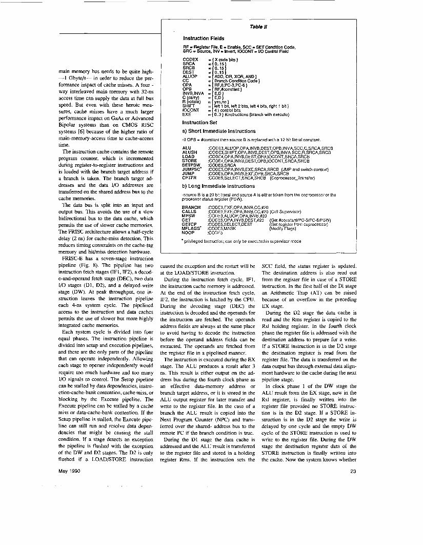
Instruction Fields
RF = Register File. E - Enable, SCC I SET Condition Code, SRC ., Source, INV = Invert, WONT I VO Control Field
CODEX = Xc~debits ) SRCA =fO..%5 SRCB 6 O..IsI
Instruction Set
a) Short immediate Instructions
-if OPB = #constant then source B is replaced with a 12 bit literal constant.
-_ - . - - - - -, -. . LOAD :CODE4.OP.
ALU :CODE3,ALUOP,OPA,INVB,DEST,OPB,INVA,SCC,C,SRCA,SRCB ALUSH C O D F R .SHIFT,OPA.INVB,DEST.OPB.INVA,SCC.R,SRCA,SRCB
A INVB DEST OPE IOCONT SRCA SRCB STORE :CODE4;OPA:INVB:DEST:OPB:IOCONT:SRCA:SRCB SETPSW CODF5 SRCA JUMPSC' :CODES:FjF;, i~lNVB.EXE.SRCA.SRCB fJMP and switch context) JUMP :CODE5;OPA;INVB;EXE;OPB,SRCA,SRCB CPTFR :CODES,SELECT.SRCA.SRCB (Coprocessor-Transfer)
b) Long Immediate Instructions
-source B is a 20 bit literal and source A is either taken from the coprocessor or the processor status register (PSW).
privileged Instruction; can only be executed in supervisor mode
caused the exception and the restart will be at the LOAD/STORE instruction.
During the instruction fetch cycle, IF1, the instruction cache memory is addressed. At the end of the instruction fetch cycle, IF2, the instruction is latched by the CPU. During the decoding stage (DEC) the instruction is decoded and the operands for the instruction are fetched. The operands address fields are always at the same place to avoid having to decode the instruction before the operand address fields can be extracted. The operands are fetched from the register file in a pipelined manner.
The instruction is executed during the EX stage. The ALU produces a result after 3 ns. This result is either output on the ad- dress bus during the fourth clock phase as an effective data-memory address or branch target address, or it is stored in the ALU output register for later transfer and write to the register file. In the case of a branch the ALU result is copied into the Next Program Counter (NPC) and trans- ferred over the shared- address bus to the remote PC if the branch condition is true.
During the D1 stage the data cache is addressed and the ALU result is transferred to the register file and stored in a holding register Rms. If the instruction sets the
SCC field, the status register is updated. The destination address is also read out from the register file in case of a STORE instruction. In the first half of the D1 stage an Arithmetic Trap (AT) can be raised because of an overflow in the preceding EX stage.
During the D2 stage the data cache is read and the Rms register is copied to the Rsl holding register. In the fourth clock phase the register file is addressed with the destination address to prepare for a write. If a STORE instruction is in the D2 stage the destination register is read from the register file. The data is transferred on the data output bus through external data align- ment hardware to the cache during the next pipeline stage.
In clock phase 1 of the DW stage the ALU result from the EX stage, now in the Rsl register, is finally written into the register file provided no STORE instruc- tion is in the D2 stage. If a STORE in- struction is in the D2 stage the write is delayed by one cycle and the empty DW cycle of the STORE instruction is used to write to the register file. During the DW stage the destination register data of the STORE instruction is finally written into the cache. Now the system knows whether
23
a cache hit or cache miss has occurred. If it is a cache miss and the cache line is dirty, the execute pipeline is stalled until the copy back and cache-line-load opera- tions have been completed. The data load- ed by a LOAD instruction must be copied into the Din register by the end of clock phase. The delay of 2 ns before the data must be copied into D, is available for external data alignment hardware. In the first half of the DW cycle an exception caused in the previous D1 cycle due to a page fault or parity error on the data cache could be raised, but only U0 instructions can be aborted once they have completed the D2 stage.
The seven-stage pipelining leads to a load and branch latency of three instructions. The three instructions after a LOAD in- struction cannot reference the destination register of the LOAD without causing a pipeline interlock since the operand register must be available during the DEC stage of each instruction (Fig. 9). The three instruc- tions following a BRANCH always enter the instruction execution pipeline before the branch can take effect.
In a monolithic implementation of FRISC the load and branch latencies could be reduced to two cycles. The branch address could be computed (PC relative) in the DEC stage by an adder specifically for branch target and address calculations since the PC and the immediate constant are already available. Further, by feeding data loaded from the cache directly to the ALU the load latency could be reduced by one cycle.
Some RISC machines always execute the instructions in the latency region [2,3]. NOOP instructions must then be inserted if a code reorganizer cannot find enough instructions to fill the latency region. Data- -dependency pipeline interlocks and a modified branch execution scheme are used for FRISC because the NOOPS required to prevent pipeline hazards increase the code size, thus reducing the effectiveness of the cache. With a modest increase in hardware complexity a flexible branch-with-execute scheme can be implemented (Fig. 10). Since branch instructions (including jumps) take branches with a probability of about 314, and the instructions in the latency region are always fetched, code optimiza- tion for pipelined machines requires the latency region to be filled with instructions that can always be executed. If not enough instructions can be found, the next instruc-
24
Figure 7 SYSTEfl BUS 0
COPROCESSOR
I
7 . FRISC-E System Overview
Figure 8 Setup Execut 1 on a W D
Fj r l f i Dm m;1 F q Instructlon Fetch I
I t ‘ Instruction Fetch 2
Instruction Fetch Operands
LExscLte I Instruction Output Addreee [LD.ST.JMP.BRhl
‘Dota l I/O I Cycle I
‘Da ta ’ I/O c cle 2/ Read Dest.’Reeieter
‘Delayed Write - 0 o t a Coche/ Oest. Regieter
8. Seven-Stage Instruction Pipeline of FRISC-E
Figure 9
ADDR TRACE PIPEL I NE
10 1 1 12 13 1 4 15 16
L O R I . [ RID 1 NOOP NOOP NOOP TST R I BE2 100 NOOP
L o a d LoLency
I? NOOP 3 Instructions
l a NOOP I00 INC R I
I
9. Load and Branch Latency
Circuits and Devices
tion in the latency region should be flushed. To implement this, branch instruc- tions have an EXE field that specifies how many instructions in the latency region (0 to 3) should be executed. A variety of branch-optimization schemes could be used to reduce branch penalties [16], but the delayed branch scheme can be implement- ed with minimal cost.
Performance FRISC-E has a peak performance of 250 MIPS. But the pipelined execution of instructions inflicts branch and load laten- cies, as well as cache misses, that reduce the integer performance (Table 3). As for FRISC-E's net performance on an average instruction mix [ 151, let's assume a system that has two 2-way interleaved 64-Kbyte caches implemented on the same WSH with 8-by-8-Kbyte memories [I], and let's use generally accepted cache-miss figures [9]. The main memory is assumed to be a four-way interleaved, 4-bit-wide memory with an access time of 32 ns, and we'll assume a system-bus-bandwidth of 1 Gbyte per second-8 bytes every 8 ns. The result- ing throughput rate is 102 MIPS without code reorganization to reduce pipelining penalties. The major performance impact comes from branch and load latencies and from instruction-cache misses reducing performance to 52 percent of peak. The latencies alone reduce performance to 52 percent of peak performance. Cache misses alone reduce performance to 68 percent.
A throughput rate of 102-MIPS is 1.45 times that of a FRISC running at 8 ns with only a three-stage instruction pipeline. However, code optimization for six-stage RISC machines can increase performance by as much as 20 percent without exhaust- ing all theoretical possibilities for optimiza- tion [17]. Code optimization can increase the performance of the 250-MIPS version with a seven-stage pipeline to between 1.5 and 1.6 times that of the 125-MIPS without using faster cache memories. CD
Acknowledgment We would like to thank Tektronix, Inc. for their support.
References 1. D. A. Patterson et al., "A VLSI RISC," IEEE Computer, pp. 8-21 (September 1982).
May 1990
Figure 10
-r \ m
Z w Y < +
-
E z 4. K
a m I
I A l I A2
I A I BRANCH CC ex.2 TRUE
I A3 BRANCH CC TRUE ;?: > executed
IcI f 1 ushed i f C z f a l s e if C=foIse IC2
only execu ted
I I C 3 1 I C3
TRUE : I B I I E2 I 8 3 I E3
BRANCH w i t h FLUSH BRANCH WITH EXECUTE
IO. Branch Execution
2. M. G. Katevenis, Reduced Instruction Set Architectures for VLSI (MIT Press, 1985). 3. J. Hennessy, "The MIPS Machine," Digest of Papers, Spring COMCON 82, San Francisco, pp. 2-7 (December 1983). 4. H. Greub et al., "Architecture of a 32 Blt Fast Reduced Instruction Set Computer (FRISC) for Implementation with Ad- vanced Bipolar Differential Logic and Wafer Scale Hybrid Packaging" in VLSI 87, pp. 275-87 (North Holland Publishing, 1988). 5. Jack F. McDonald et al., "Wafer Scale Interconnections for GaAs Packaging - Applications to RISC Architecture," IEEE Computer, pp. 21-35 (April 1987). 6. V. M. Milutinovic et al., Gallium Arse- nide Computer Design (IEEE Computer Society Press, 1988). 7. B. Donlan et al., "The Wafer Transmis- sion Module," VLSI Systems Design, pp. 54-90 (January 1986). 8. A. J. Blodgett et al., "Thermal Conduc- tion Module: A High Performance Multila- yer Ceramic Package," IBM J. of Res. and Dev. (Jan. 1982). 9. Alan Jay Smith, "Line (Block) Size Choice for CPU Cache Memories," IEEE Transactions on Computers, pp. 1063-75, Vol. C-36, No. 9 (September 1987). 10. Tomoharu Awaya et al., "A 5ns Access Time 64Kb ECL RAM," IEEE Solid-state Circuit Conference; ISSCC 87, pp. 130-- 131. 11. Hee K. Park et al., "High-speed Polysi- licon Emitter Base Bipolar Transistor," IEEE Electron Device Letters, pp. 39-40, Vol. EDL-7, No.12 (December 86, pp.
12. Tadanori Yamaguchi et al., "Process and Device Performance of a High-speed
39-40).
Double Poly-Si Bipolar Technology Using Borosenic-Poly Process wjth Coupling Implant," IEEE Transactions on Electron Devices, pp. 1247-55, Vol. 35, No. 8 (Au- gust 1988). 13. H. J. Greub et al., "Key Components of the Fast Reduced Instruction Set Computer (FRISC) Employing Advanced Bipolar Differential Logic and Wafer Scale Multi- chip Packaging," Proceedings of 1988 Bipolar Circuits and Technology Meeting (To be published). 14. G. Radin, "The 801 Minicomputer," IBM J. of Res. and Dev., pp. 237-45, Vol. 27, No. 3 (May 1983). 15. Masood Namjoo et al., "Implementing SPARC: A High Performance 32-Bit RISC Microprocessor," Sun Technology, pp. 42-48 (Winter 1988). 16. David J. Lilja et al., "Reducing the Branch Penalty in Pipelined Processors, IEEE Computer, pp. 47-55 (July 1988). 17. Veljko Milutinovic et al., "Architectur- e/Compiler Synergism in GaAs Computer Systems," IEEE Computer, pp. 72-93 (May 1987).
Biographies Hans J. Greub is a Ph.D. student and Fulb- right Scholar at Rensselaer Polytechnic Institute, Institute of Integrated Electronics, and is currently Tek Fellow. Jack F. McDonald is a full professor in the Electrical, Computer and Systems Engi- neering Department at Rensselaer Polytech- nic Institute in Troy, New York, and a founding member of RPI's Center for Integrated Electronics. Theodore G. Creedon is manager of the Systems Integration Group at Tektronix Laboratories in Beaverton, Oregon.