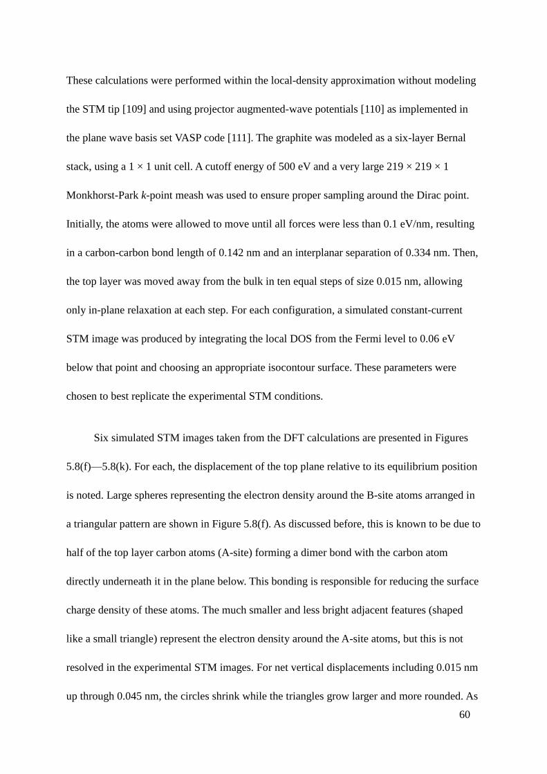
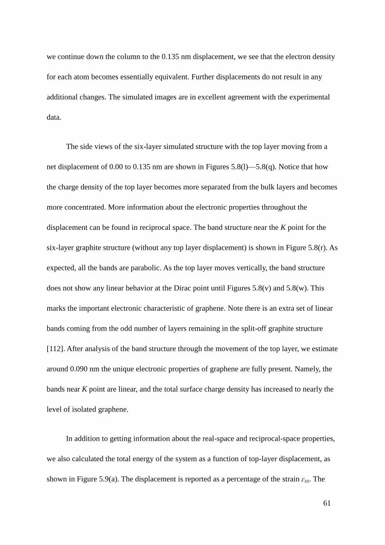
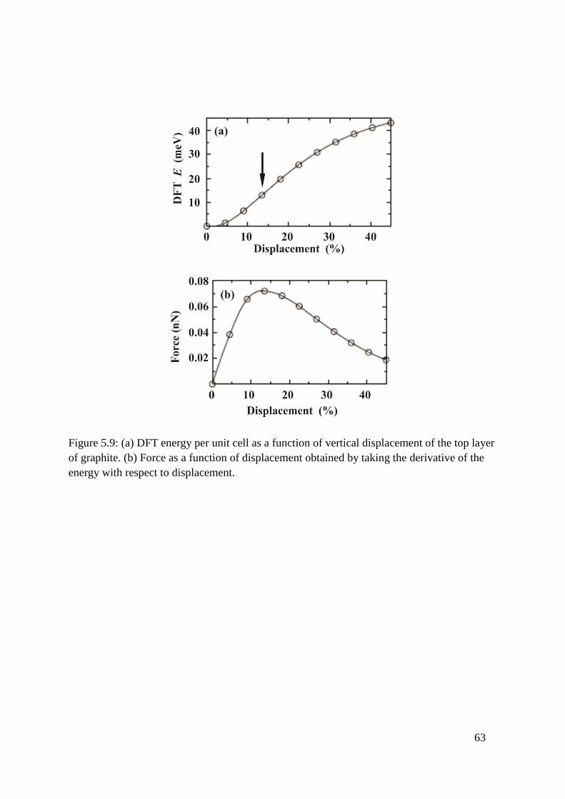
Page 1
University of Arkansas, FayettevilleScholarWorks@UARK
Theses and Dissertations
8-2014
From Graphite to Graphene via ScanningTunneling MicroscopyDejun QiUniversity of Arkansas, Fayetteville
Follow this and additional works at: http://scholarworks.uark.edu/etd
Part of the Quantum Physics Commons
This Dissertation is brought to you for free and open access by ScholarWorks@UARK. It has been accepted for inclusion in Theses and Dissertations byan authorized administrator of ScholarWorks@UARK. For more information, please contact [email protected] , [email protected] .
Recommended CitationQi, Dejun, "From Graphite to Graphene via Scanning Tunneling Microscopy" (2014). Theses and Dissertations. 2195.http://scholarworks.uark.edu/etd/2195
Page 2
From Graphite to Graphene via Scanning Tunneling Microscopy
Page 3
From Graphite to Graphene via Scanning Tunneling Microscopy
A dissertation submitted in partial fulfillment
of the requirements for the degree of
Doctor of Philosophy in Physics
by
Dejun Qi
Harbin University of Science & Technology
Bachelor of Science in Physics, 2005
Chinese Academy of Science
Master of Science in Physics, 2008
August 2014
University of Arkansas
This dissertation is approved for recommendation to the Graduate Council.
__________________________________
Dr. Paul Thibado
Dissertation Director
__________________________________ __________________________________
Dr. Huaxiang Fu Dr. Jiali Li
Committee Member Committee Member
__________________________________ __________________________________
Dr. Ryan Tian Dr. Jacques Chakhalian
Committee Member Committee Member
Page 4
ABSTRACT
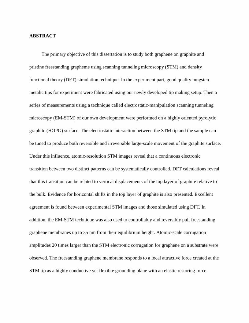
The primary objective of this dissertation is to study both graphene on graphite and
pristine freestanding grapheme using scanning tunneling microscopy (STM) and density
functional theory (DFT) simulation technique. In the experiment part, good quality tungsten
metalic tips for experiment were fabricated using our newly developed tip making setup. Then a
series of measurements using a technique called electrostatic-manipulation scanning tunneling
microscopy (EM-STM) of our own development were performed on a highly oriented pyrolytic
graphite (HOPG) surface. The electrostatic interaction between the STM tip and the sample can
be tuned to produce both reversible and irreversible large-scale movement of the graphite surface.
Under this influence, atomic-resolution STM images reveal that a continuous electronic
transition between two distinct patterns can be systematically controlled. DFT calculations reveal
that this transition can be related to vertical displacements of the top layer of graphite relative to
the bulk. Evidence for horizontal shifts in the top layer of graphite is also presented. Excellent
agreement is found between experimental STM images and those simulated using DFT. In
addition, the EM-STM technique was also used to controllably and reversibly pull freestanding
graphene membranes up to 35 nm from their equilibrium height. Atomic-scale corrugation
amplitudes 20 times larger than the STM electronic corrugation for graphene on a substrate were
observed. The freestanding graphene membrane responds to a local attractive force created at the
STM tip as a highly conductive yet flexible grounding plane with an elastic restoring force.
Page 5
ACKNOWLEDGMENTS
Special thanks are due to my advisor Dr. Paul Thibado who has patiently guided me
through these years of research and time spent discussing lots of details in my research work
with me. It would be impossible to finish this dissertation without his generous help. I was
immature and my attitude to my work was so wrong at the beginning I joined this group, thanks
to both Dr. Thibado’s criticism and encouragement I eventually understand the purpose of my
career and the importance of having a right attitude. Also, special thanks go out to Dr. Peng Xu
for his valuable suggestions and constant help on improving the dissertation. His generous
support and knowledge sharing helped me get rid of lots of difficulties on experiment techniques.
I would also like to thank Matt Ackerman, Steven Barber, Kevin Schoelz, Dr. Yurong Yang, Dr.
Laurent Bellaiche and Dr. Salvador Barraza-Lopez for their cooperation and help.
Meanwhile, I would also like to give my special thanks to all my advisory committee
members for their guidance and encouragement through these years. Especially, Dr. Huxiang Fu,
Dr. Jiali Li, as my lecturers of core courses such as Statistical Physics, Optical Properties of
Materials, and Electrodynamics, their rigorous teaching attitudes and profound knowledge also
benefit my research in various aspects.
Also, I would like to thank my parents, my relatives and my friend who continuously
deliver their care, love, and support to me all these years. Whenever I come across setbacks and
frustration I know that they are with me. I am deeply grateful to them. Finally, I am thankful to
Page 6
those setbacks and frustrations that I came across these years, seriously, since without all these
things happened to me I am probably still an overgrown boy.
Page 7
TABLE OF CONTENTS
CHAPTER 1 INTRODUCTION ............................................................................................... 1
CHAPTER 2 GRAPHITE AND GRAPHENE .......................................................................... 7
2.1 Background ..................................................................................................................... 7
2.2 Graphite and graphene .................................................................................................. 10
CHAPTER 3 SCANNING TUNNELING MICROSCOPY .................................................... 18
3.1 Background ................................................................................................................... 18
3.2 Electron tunneling ......................................................................................................... 18
CHAPTER 4 EXPERIMENTAL DETAILS ............................................................................ 26
4.1 STM tip making ............................................................................................................ 26
4.2 Samples preparation ...................................................................................................... 39
4.2 Electrostatic manipulation-STM (EM-STM) ................................................................ 40
CHAPTER 5 GRAPHENE ON GRAPHITE .......................................................................... 45
5.1 Surface morphology of graphite ................................................................................... 46
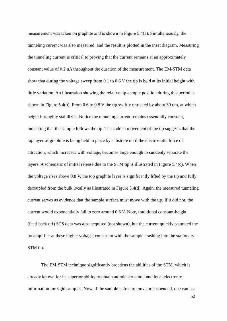
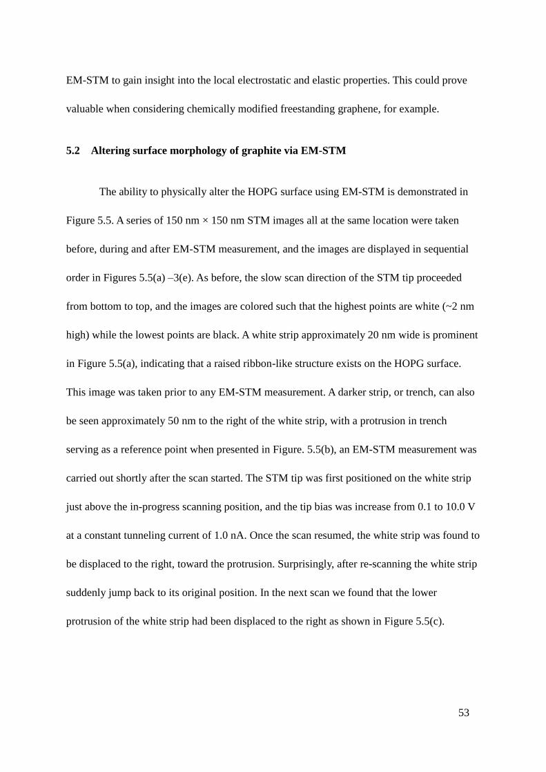
5.2 Altering surface morphology of graphite via EM-STM ............................................... 53
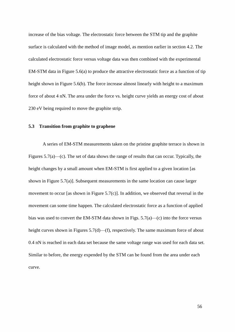
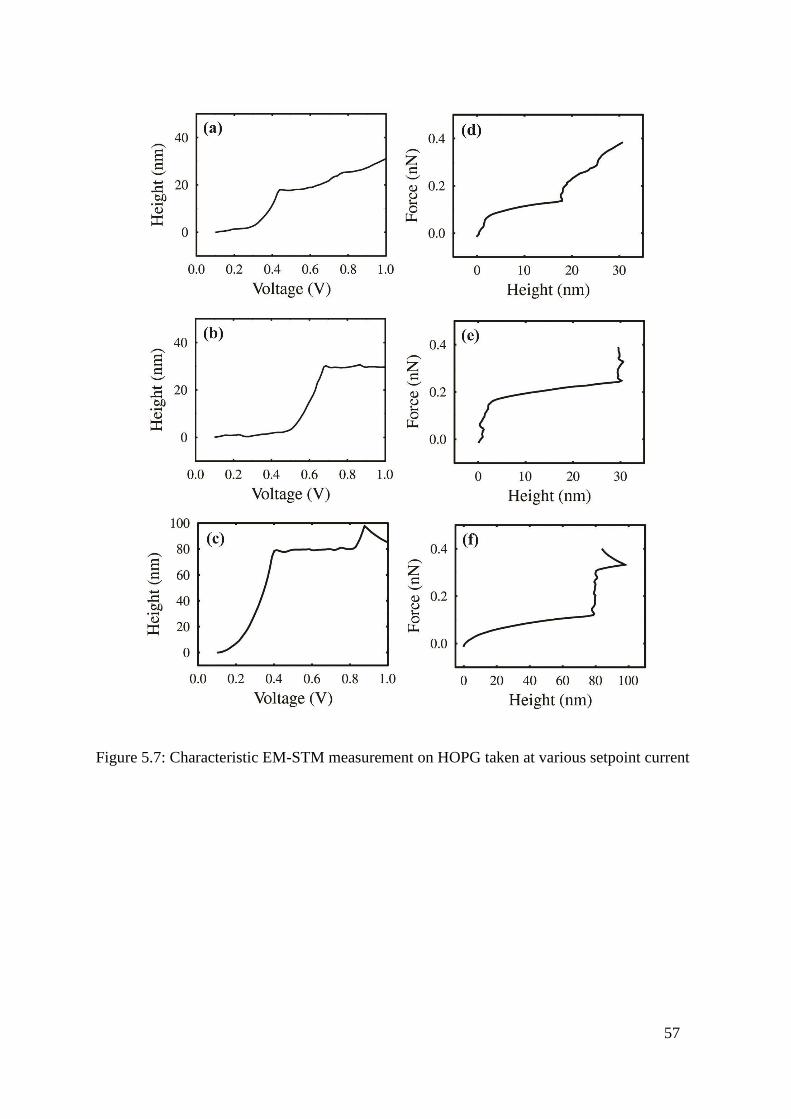
5.3 Transition from graphite to graphene ............................................................................ 56
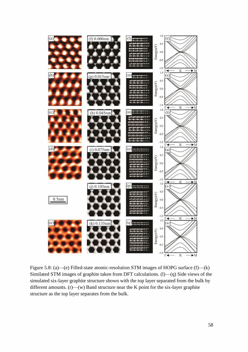
5.4 Bernal (ABA) and rhombohedral (ABC) stacking ....................................................... 67
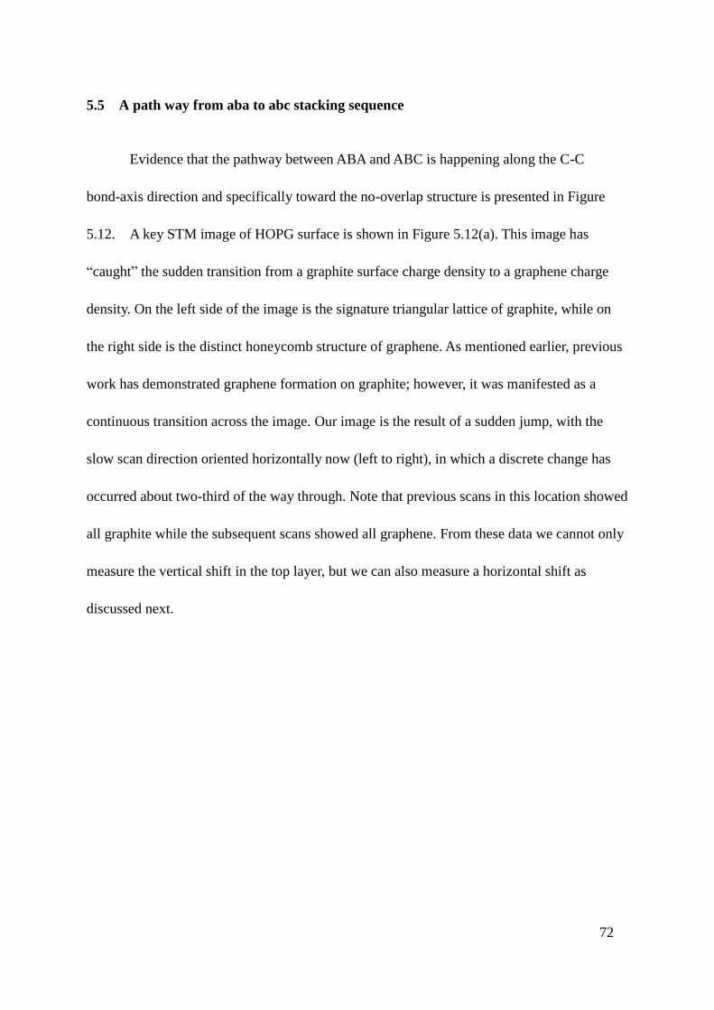
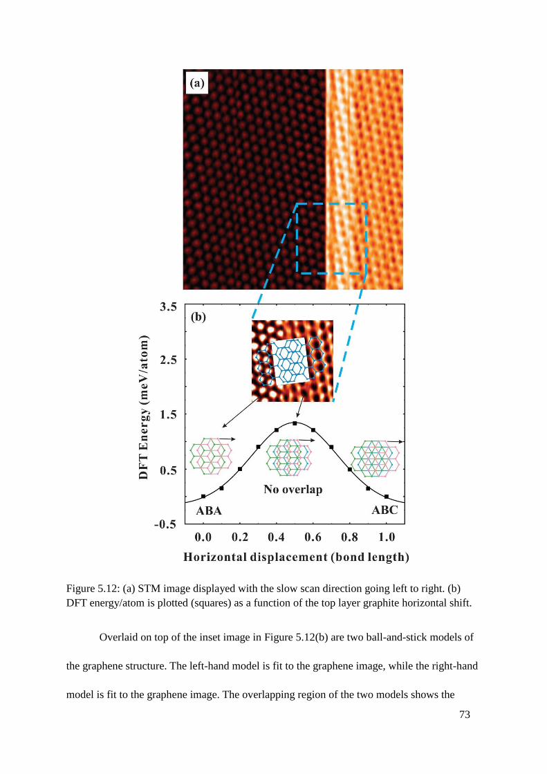
5.5 A path way from aba to abc stacking sequence ............................................................ 72
CHAPTER 6 GRAPHENE SUSPENDED ON TEM GRID ................................................... 76
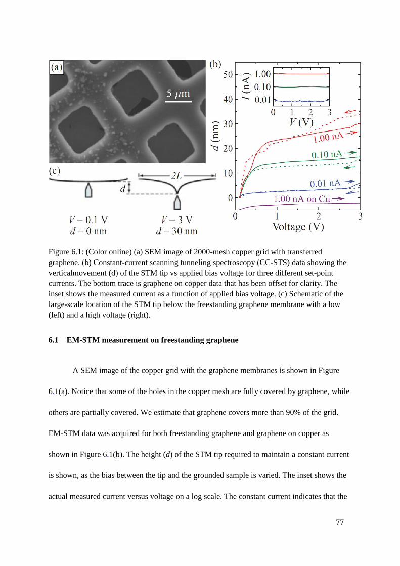
6.1 EM-STM measurement on freestanding graphene ....................................................... 77
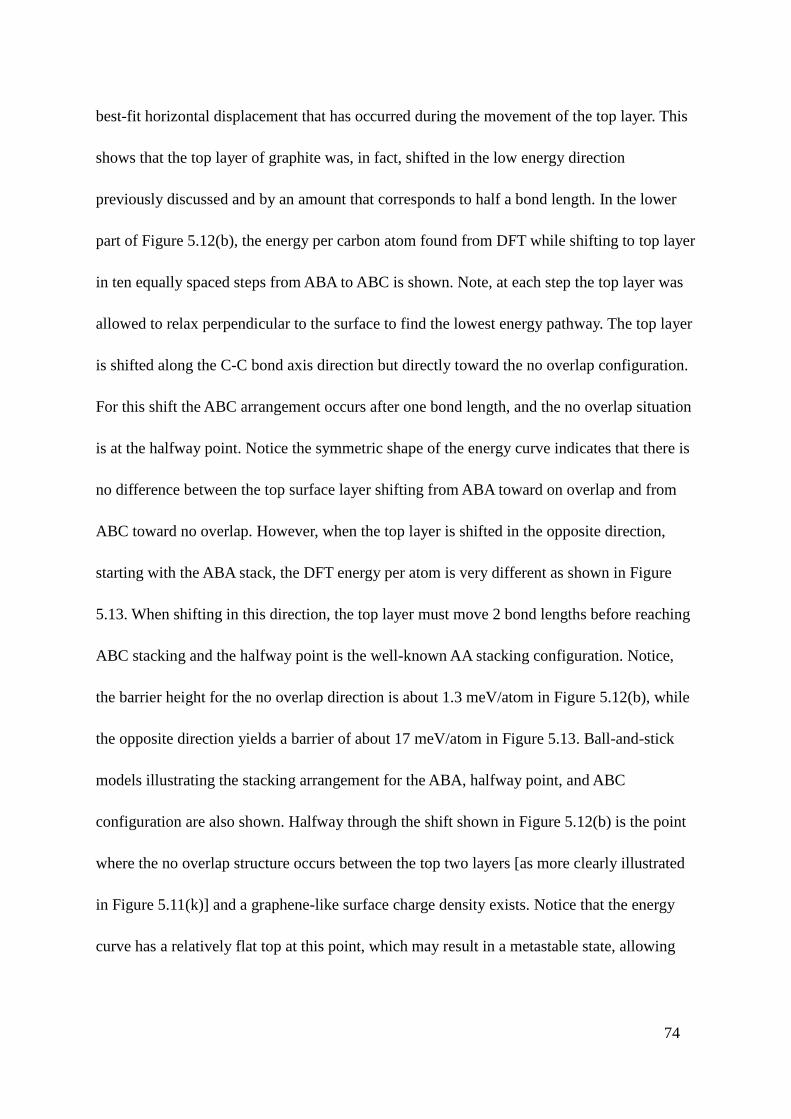
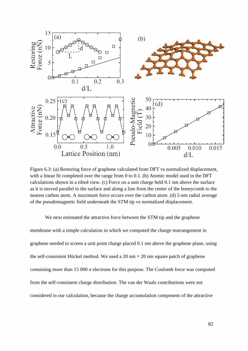
6.2 Fluctuation of the attractive force ................................................................................. 80
CHAPTER 7 SUMMARY AND CONCLUSION ................................................................... 87
BIBLIOGRAPHY ......................................................................................................................... 91
Page 8
1
CHAPTER 1 INTRODUCTION
When a material is cut from a surface, the broken bonds tend to rearrange into a lower
energy configuration. This process is known as a surface reconstruction and results in surface
atoms having a different symmetry from the bulk atoms. For example, on the Si(001) surface
adjacent Si atoms will till toward each other to form a dimer bond. In doing so, half of the
broken surface bonds can be reformed to significantly lower the total surface energy. The
symmetry of the surface is now different from the bulk since the periodicity along the dimer
bond is twice the bulk, thereby yielding a (2 ×1) surface reconstruction [1, 2, 3, 4, 5]. Similar
things happen on the GaAs(001) surface [6, 7, 8], but here the atomic arrangement is
dependent on the arsenic pressure as well as the substrate temperature. In some instances a
phase transition can be identified between the various reconstructions [9]. At the other
extreme, a more subtle surface reconstruction can occur which involves only the electron
distribution within the material. A prime example is the easily cleaved GaAs(110) surface,
which exhibits very weak bonding between layers [10]. Because of this, when the layers are
separated, the atomic nuclear positions remains the same, but the surface charge density
significantly redistributes itself. The charge shifts to be only on the surface As atoms instead
of being equally shared between the Ga and As atoms. Consequently, scanning tunneling
microscopy (STM) filled-state images show only the As atoms, while empty-state images
shows only the Ga atoms.
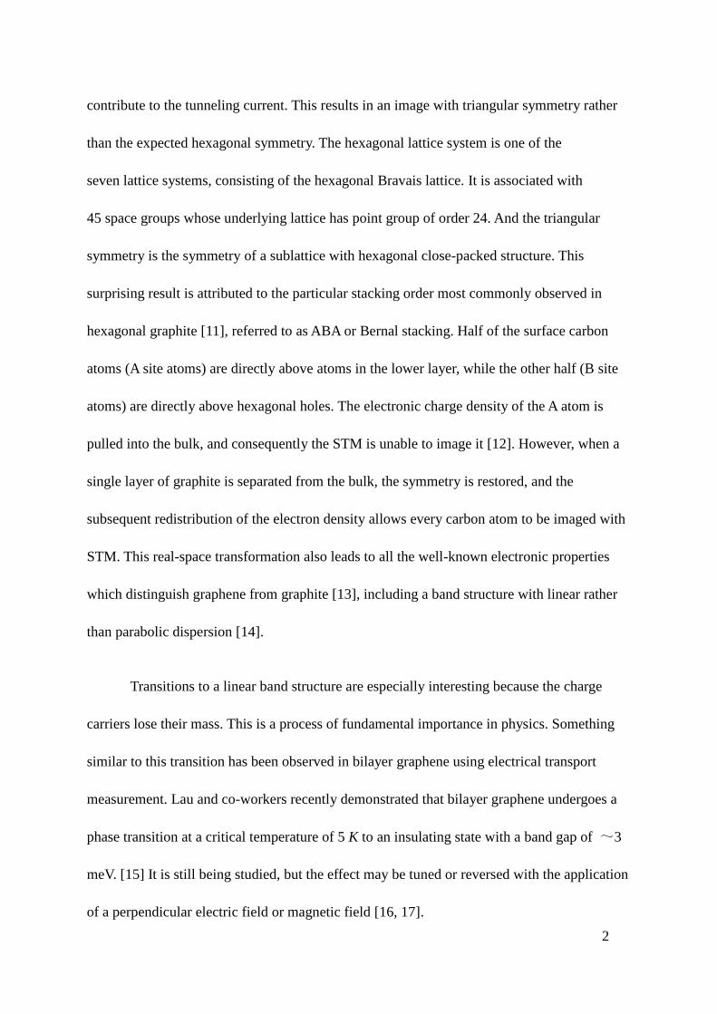
Similar to GaAs, highly oriented pyrolitic graphite (HOPG) is another example of a
system which is easily cleaved. When HOPG is imaged using STM, only alternate atoms
Page 9
2
contribute to the tunneling current. This results in an image with triangular symmetry rather
than the expected hexagonal symmetry. The hexagonal lattice system is one of the
seven lattice systems, consisting of the hexagonal Bravais lattice. It is associated with
45 space groups whose underlying lattice has point group of order 24. And the triangular
symmetry is the symmetry of a sublattice with hexagonal close-packed structure. This
surprising result is attributed to the particular stacking order most commonly observed in
hexagonal graphite [11], referred to as ABA or Bernal stacking. Half of the surface carbon
atoms (A site atoms) are directly above atoms in the lower layer, while the other half (B site
atoms) are directly above hexagonal holes. The electronic charge density of the A atom is
pulled into the bulk, and consequently the STM is unable to image it [12]. However, when a
single layer of graphite is separated from the bulk, the symmetry is restored, and the
subsequent redistribution of the electron density allows every carbon atom to be imaged with
STM. This real-space transformation also leads to all the well-known electronic properties
which distinguish graphene from graphite [13], including a band structure with linear rather
than parabolic dispersion [14].
Transitions to a linear band structure are especially interesting because the charge
carriers lose their mass. This is a process of fundamental importance in physics. Something
similar to this transition has been observed in bilayer graphene using electrical transport
measurement. Lau and co-workers recently demonstrated that bilayer graphene undergoes a
phase transition at a critical temperature of 5 K to an insulating state with a band gap of ~3
meV. [15] It is still being studied, but the effect may be tuned or reversed with the application
of a perpendicular electric field or magnetic field [16, 17].
Page 10
3
Studies using graphite have observed similar things; however, the events are
randomly occurring, and thought to arise from preexisting defects in graphite. For example,
using low-temperature (4.4 K) STM, low-voltage scanning tunneling spectroscopy (STS), and
a magnetic field, Landau levels consistent with graphene have been observed on graphite by
Andrei and co-workers [18, 19]. Signatures in the sequence have been used to quantitatively
predict the amount of interaction between the top layer and the bulk. Further evidence of
varying degrees of coupling can be seen in the symmetry of STM images. The STM tip can
provide a perturbation that vertically lifts the top layer, resulting in images which exhibit a
range of possibilities between the triangular and hexagonal lattices [20]. The difficulty,
however, is that this induced decoupling has been random, not lending itself to a systematic
study of the important symmetry-breaking transition from bulk graphite to monolayer
graphene.
A surface charge density similar to graphene but on graphite can also be attributed to
horizontal shifts in the surface layer [21, 22]. This has created a lot of excitement in
potentially controlling the stacking of graphene layers. For example, recent work suggest that
stacking graphene is a way to solve the band gap problem, which is currently the chief
obstacle for using graphene in digital electronic devices. Trilayer graphene is especially
interesting because two stable allotropes have been identified; the layers can be arranged with
ABA (Bernal) stacking or ABC (rhombphedral) stacking. ABC trilayers exhibit an inherent
band gap of ~6 meV at the K point [23], which can be increased by applying an electrical
field, while no such band gap is predicted in ABA trilayers.
Page 11
4
Naturally, several major steps have been taken toward characterizing the stacking
sequence. For instance, Raman spectroscopy performed on mechanically exfoliated graphene
has revealed that the majority of trilayers produced are ABA stacked, while only 15% are in
the ABC configuration [24, 25]. On the other hand, when graphene is grown on SiC(0001),
the layers selectively form in ABC order over ABA, as observed with high-resolution
transmission electron microscopy [26]. Certainly, one would like to control the stacking
sequence or ideally alter it from one form to the other. A related area with a lot of interest is
rotated or twisted layers [27, 28]. This has a lot of appeal because all the physics can be
parameterized with just one angle. Horizontal shifting has received less attention [29].
On the other hand, in most graphene studies, samples are on a substrate, which
degrades the intrinsic mobility of graphene [30]. The mechanisms behind this degradation
include local effects, such as charged-impurity scattering, and nonlocal phenomena, such as
phonon scattering [31]. Scanning tunneling microscopy (STM) and spectroscopy (STS) [32,
33] reveal that charge-donating substrate impurities create charge puddles in supported
graphene. The numerous limitations associated with examining graphene on substrates have
led researchers to suspend graphene over holes [ 34 35] to better study its intrinsic properties.
These efforts have been rewarded with many important breakthroughs, including the
measurement of its record breaking ballistic carrier mobility [36], thermal conductivity [37],
and the fractional Quantum Hall Effect [38]. Freestanding graphene has also provided a way
to probe the material’s intrinsic tensile strength [39, 40]. Atomic force microscopy, combined
with other techniques, has been utilized to measure its effective spring constant, resonance
frequency (in the megahertz range) [41], Young’s modulus, self-tension, and the breaking
Page 12
5
strength of single- and multiple-layer graphene [42, 43]. More recently, STM has been used
to create minimembranes by locally lifting graphene from the substrate [44]. In addition,
through the distortion of the two-dimensional plane with strain, the properties of charge
carriers in graphene have been found to change dramatically as gauge fields (pseudomagnetic
and deformation potential) are created [45, 46, 47, 48]. Researchers using transmission
electron microscopy pioneered the efforts of imaging freestanding graphene, providing
insight into the existence of ripples [49] and revealing point defects and ring defects, as well
as edge reconstructions [50].
In this dissertation I am going to discuss our research of graphene that is coupled with
the bulk graphite substrate, and focuses on the transition from graphene that is coupled with
undelying layer to a single layer of graphene. I will present STM images of the HOPG
surface before, during, and after perturbing the surface using a technique called
electrostatic-manipulation STM (EM-STM) [51]. With this technique large-scale
precision-controlled vertical movement of the graphite surface is possible. Atomic-scale STM
images reveal a continuous transition from graphite lattice symmetry to grapheme lattice
symmetry. Density functional theory calculations were used to generate a complete set of
simulated STM images and provide excellent agreement with the measurements. The
continuous change in the spatial distribution of the charge density is proposed as a measure of
coupling between the surface layer and the bulk. Next, STM images on HOPG surface which
show clear evidence of the top layer shifting horizontally in a direction along carbon-carbon
(C-C) bond axis will be presented. Excellent agreement with a series of DFT simulated
images generated from structures shifted along this same direction is also presented. From
Page 13
6
DFT we predicted the direction for the lowest-energy barrier to transition from ABA to ABC
stacking.
In the next chapter, our research result of freestanding graphene on TEM grid will be
discussed. I will describes the EM-STM measurement on freestanding graphene and
introduce a strain in a controlled way onto the freestanding graphene. Also, I’ll show our
atomic-resolution STM images of freestanding graphene and document vertical corrugations
(d) that are 20 times larger than the expected electronic corrugation (de) due to strain-induced
movement (u, where d = de + u).
Page 14
7
CHAPTER 2 GRAPHITE AND GRAPHENE
2.1 Background
Carbon is one of the most abundant elements in earth and the basis of all organic
chemistry. Due to its flexible bonding, carbon materials form a series of different structures
with an equally large variety of physical properties. Graphene, a newly discovered
two-dimensional (2D) allotrope of carbon atoms with hexagonal lattice layer structure, plays
an important role in understanding the electronic properties of other carbon allotropes. For
example, carbon nanotubes [52, 53] can be obtained by rolling graphene along a given
direction and reconnecting the carbon bonds on the edges of the sheet. Therefore, carbon
nanotubes consist of only carbon hexagons and can be thought of as one-dimensional (1D)
carbon allotropes. Graphite, a three dimensional (3D) allotrope of carbon, became well
known since the pencil was invented in 1564 [54]. It is highly applicable as a tool of writing
due to the fact that graphite is made out of stacks of graphene sheets that are weakly coupled
by the van der Waals interaction. It is interesting to imagine that as we are writing on a piece
of paper with a pencil, we are actually producing graphene stacks and, somewhere among
them, there could even be single graphene layers. Despite the ubiquity of graphene among all
these different allotropes and the likelihood of producing of graphene every time we write
with a pencil over a paper, graphene was not able to be isolated and identified until 440
hundred years after the pencil was invented [55]. In fact, initially no one expected graphene
to exist in the free state because of lacking experimental technique that was capable of
searching for one-atom-thick carbon layers among the pencil debris covering macroscopic
Page 15
8
areas [56]. While graphene was eventually isolated and identified via its subtle optical effect
as it is transferred on top of a well-chosen SiO2 substrate which allows it to be observed with
an ordinary optical microscope [57, 58, 59]. Therefore, graphene is relatively straightforward
to produce, but quite difficult to find.
The structural flexibility of graphene is manifested by its electronic properties. The
sp2 hybridization between one s- orbit and two p-orbits leads to the formation of a σ bond
between nearest carbon atoms that are separated by 1.42 Å. This special hybridization
therefore gives rise to a triangular layer structure. The formation of σ band is the key to the
robustness of the lattice structure for all carbon allotropes. According to the Pauli principle,
these bands contain a filled shell and, as a result, form a deep valence band. The unaffected
p-orbit, which is perpendicular to the trigonal planar structure, can be weakly bonded with
neighboring carbon atoms, resulting in the formation of a π band. Unlike the σ band, since
every p-orbit has one extra electron, the π band is half filled.
Half-filled bands for transition elements in the periodic table play an important role in
the physical properties of strongly correlated systems. Because of their strong tight-binding
character, the Coulomb energies are so large that these transition elements have strong
collective effects, magnetism, and insulating behavior due to correlation gaps [60]. In fact, it
was proposed by Linus Pauling in the 1950s that, based on the electronic properties of
benzene, graphene should be a resonant valence bond (RVB) structure. RVB states have
become a popular topic in the research of transition-metal oxides, and particularly in the
research of cuprate-oxide superconductors [61]. This point of view is, in fact, contrasted with
Page 16
9
contemporary research in band-structure of graphene [62] which was found to be semimetal
having an unusual linear dispersing electronic excitations called Dirac electrons. However,
most of the current experimental researches in graphene support the recent view point of band
structure. In 1946, P. R. Wallace first derived the theory of the band structure of graphene
and showed that the graphene processes an unusual semimetallic behavior [62]. At that time,
realization of 2-D material was still thought to be impossible and Wallace’s theory of
graphene band structure became the starting point to the study of graphite. In the following
years, graphite had been extensively studied. In particular, the theory of the
Slonczewski-Weiss-McClure (SWM) band structure of graphite perfectly describe the
electronic properties of this material [63, 64] and was successfully proved by experiments [65,
66, 67, 68, 69]. In 1968, the research of Schroeder et al.[70] revealed the currently accepted
location of electron and hole pockets [71]. Recent years, SWM model has been restudied as it
came across a problem of describing the van der Waals–like interactions between graphene
planes. This problem requires a thorough understanding of many-body effects that go beyond
the band-structure theorem [72]. Even as these issues do not arise in the context of a single
layer graphene, they are important for multiple graphene layers stack on top of each other, as
in the case, for instance, graphite. Stacking of graphene sheets change the electronic
properties considerably and, therefore, the layering structure can be used in order to control
the electronic properties of stacking graphene crystals. Due to the interlayer coupling, single
layer graphene processes very different transport properties than graphite or few-layer
graphene. As the charge carriers in this one-carbon atom thick thin film are confined into a
two dimensional structure, one can look for and observe the quantum Hall effect.
Page 17
10
Furthermore, in the case of a single graphene layer, its behavior differs drastically from the
case of quantum wells in conventional semiconductor interfaces which has been well studied.
In this chapter, I am going to discuss the crystal structure and the electronic structure of these
two highly related while essentially different substances: graphene and graphite.
2.2 Graphite and graphene
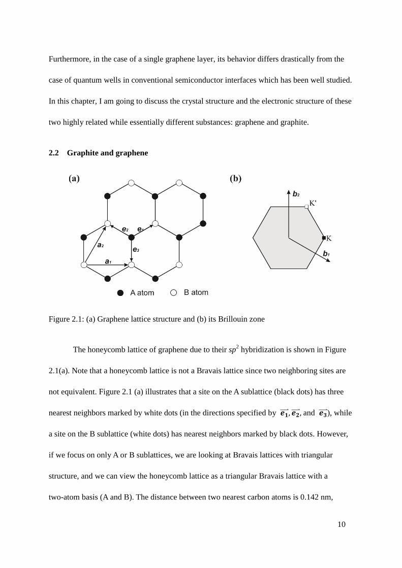
Figure 2.1: (a) Graphene lattice structure and (b) its Brillouin zone
The honeycomb lattice of graphene due to their sp2 hybridization is shown in Figure
2.1(a). Note that a honeycomb lattice is not a Bravais lattice since two neighboring sites are
not equivalent. Figure 2.1 (a) illustrates that a site on the A sublattice (black dots) has three
nearest neighbors marked by white dots (in the directions specified by 𝒆𝟏 , 𝒆𝟐 , and 𝒆𝟑 ), while
a site on the B sublattice (white dots) has nearest neighbors marked by black dots. However,
if we focus on only A or B sublattices, we are looking at Bravais lattices with triangular
structure, and we can view the honeycomb lattice as a triangular Bravais lattice with a
two-atom basis (A and B). The distance between two nearest carbon atoms is 0.142 nm,
Page 18
11
which is the average of the single and double covalent σ-bonds. The three vectors which
connect an A-site carbon atom with a nearest neighbor B-site carbon atom are written as the
following forms:
𝒆1 = 𝑎
2(√3�� + ��) (2.1)
𝒆2 = 𝑎
2(−√3�� + ��) (2.2)
𝒆1 = −𝑎�� (2.3)
and the triangular Bravais lattice is spanned by the basis vectors
𝒂1 = √3𝑎�� (2.4)
𝒂2 =√3
2𝑎(�� + √3��) (2.5)
The lattice spacing of graphene is 𝑑 = √3𝑎 = 0.24 nm, and the area of one unit cell
is Auc = 0.051 nm2. The corresponding reciprocal lattice of graphene lattice with the first
Brillouin zone (inner hexagon) is displayed in Figure 2.1(b), 𝒃1 and 𝒃2
are two reciprocal
lattice unit vectors. Because the hexagonal graphene lattice consists of only carbon atoms, for
both real space and k-space the crystal lattices can be described by two in-equivalent
triangular sublattices. As a result, in the real space two neighboring carbon atoms occupy
non-equivalent sites [as shown in Figure 2.3(b)] with black dots and white dots. The band
structure of graphene can be calculated by tight-binding approach using a separate Bloch
function ansatz for the two inequivalent lattice sites [62]. The resulting dispersion of E versus
k has the following form:
Page 19
12
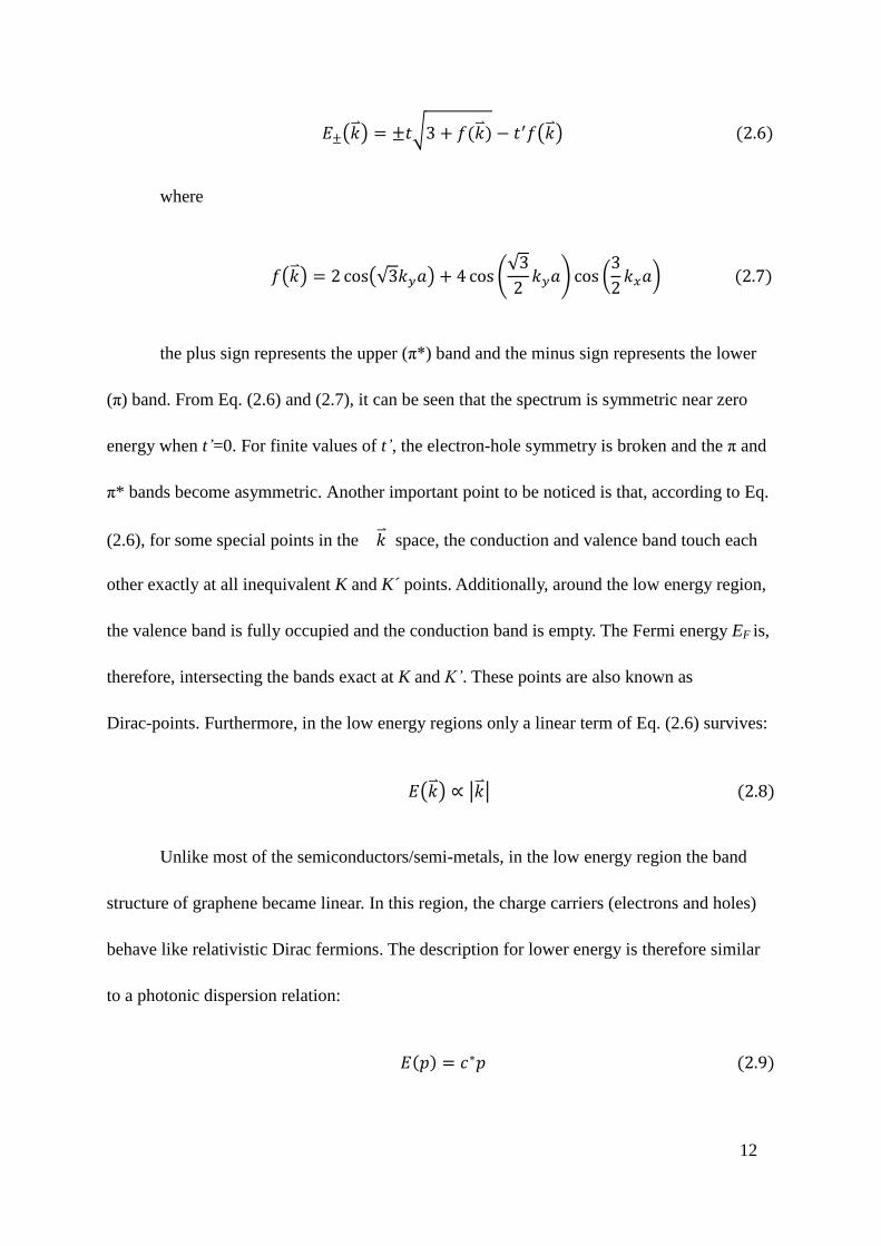
( ) = √3 + ( ) − ( ) (2. )
where
( ) = 2 (√3 𝑎) + 4 (√3
2 𝑎) (
3
2 𝑎) (2. )
the plus sign represents the upper (π*) band and the minus sign represents the lower
(π) band. From Eq. (2.6) and (2.7), it can be seen that the spectrum is symmetric near zero
energy when t’=0. For finite values of t’, the electron-hole symmetry is broken and the π and
π* bands become asymmetric. Another important point to be noticed is that, according to Eq.
(2.6), for some special points in the space, the conduction and valence band touch each
other exactly at all inequivalent K and K points. Additionally, around the low energy region,
the valence band is fully occupied and the conduction band is empty. The Fermi energy EF is,
therefore, intersecting the bands exact at K and K’. These points are also known as
Dirac-points. Furthermore, in the low energy regions only a linear term of Eq. (2.6) survives:
( ) ∝ | | (2.8)
Unlike most of the semiconductors/semi-metals, in the low energy region the band
structure of graphene became linear. In this region, the charge carriers (electrons and holes)
behave like relativistic Dirac fermions. The description for lower energy is therefore similar
to a photonic dispersion relation:
(𝑝) = 𝑐∗𝑝 (2.9)
Page 20
13
where c* is the effective speed of light 𝑐∗ ≈ 106m/s. As we know, if the speed of a particle is
much smaller than the speed of light, the Einstein relativistic dispersion transits to
non-relativistic form:
= √𝑚2𝑐4 + 𝑐2ℏ2 2 ≈ 𝑚𝑐2 +ℏ2 2
2𝑚 (2.10)
and this particle is massive, as can be seen from the Eq. (2.10). While for grahene, the Eq.
(2.9) is analog to the Einstein relativistic dispersion = √𝑚2𝑐4 + 𝑐2ℏ2 2 with mass equal
zero (m=0). As a consequence, the effective mass of the charge carriers in graphene is zero,
m= 0 [73, 74]. Together with the linear dispersion relation it can be demonstrated that the
charge carriers in graphene must be described by relativistic Dirac equation [31, 75].
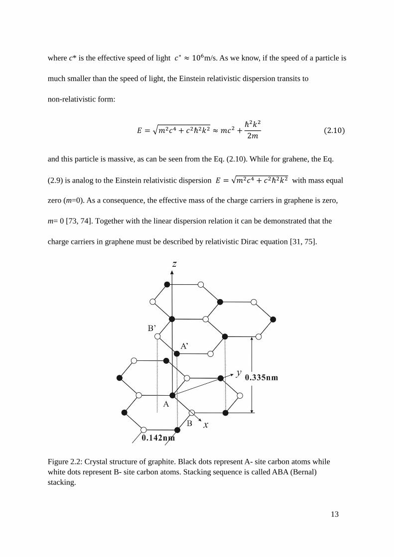
Figure 2.2: Crystal structure of graphite. Black dots represent A- site carbon atoms while
white dots represent B- site carbon atoms. Stacking sequence is called ABA (Bernal)
stacking.
Page 21
14
As multiple graphene layers are stacked together, the electronic properties of them
changes dramatically due to coupling between layers and they, as a whole, eventually become
essentially another substance—graphite. In graphite, these graphene layers are stacked in the
ABA sequence and bound in the c-direction by weak van de Waals forces. There are four
atoms per unit cell, as labeled by A, A’ and B, B’ in Figure 2.2. The atoms A and B are on the
lower layer plane and the atom A’ and B’ are on the upper layer plane, the two planes are
separated by half the crystallographic c-axis spacing (0.335 nm). As described in the last
section, the A atoms differ from B atoms in that the A atoms have neighbors directly above
and below in adjacent layers whereas the B atoms locate at the hollow site of the hexagons of
adjacent layers [76], they are the two atoms that occupy the two different sublattice sites. The
same as graphene, overlap of these sp2
hybridized orbits leads to the formation of 𝜎-bond
between nearest carbon atoms on a layer plane. While the 2pz electron forms a delocalized
orbital of π symmetry. This delocalization leads to loosely bound π-electrons with high
mobility, the π- electrons therefore determines most of the electronic properties of graphite.
In addition, graphite is anisotropic, with different physical properties for inplane and c-axis
crystallographic directions. The translation vectors (in Cartesian coordinates) of the graphite
crystal structure, as shown in Figure 2.2,
𝒂𝟏 = 𝑎 (√3
2,−
1
2, 0) (2.11)
𝒂𝟐 = 𝑎 (√3
2,+
1
2, 0) (2.12)
Page 22
15
𝒂𝟑 = 𝑐(0, 0, 1) (2.13)
where
|𝒂𝟏 | = 𝑎 = 0.24 nm (2.14)
|𝒂𝟐 | = 𝑎 = 0.24 nm (2.15)
|𝒂𝟑 | = 𝑐 = 0. 1nm (2.1 )
the lattice parameter is 𝑎 = √3𝑎0, where 𝑎0 = 1.42 𝑛𝑚, it is the in-plane distance
between two nearest neighbors. 𝑐 = 2𝑐0, where 𝑐0 = 3.35 𝑛𝑚, it is the distance between
two carbon adjacent layers.
Page 23
16
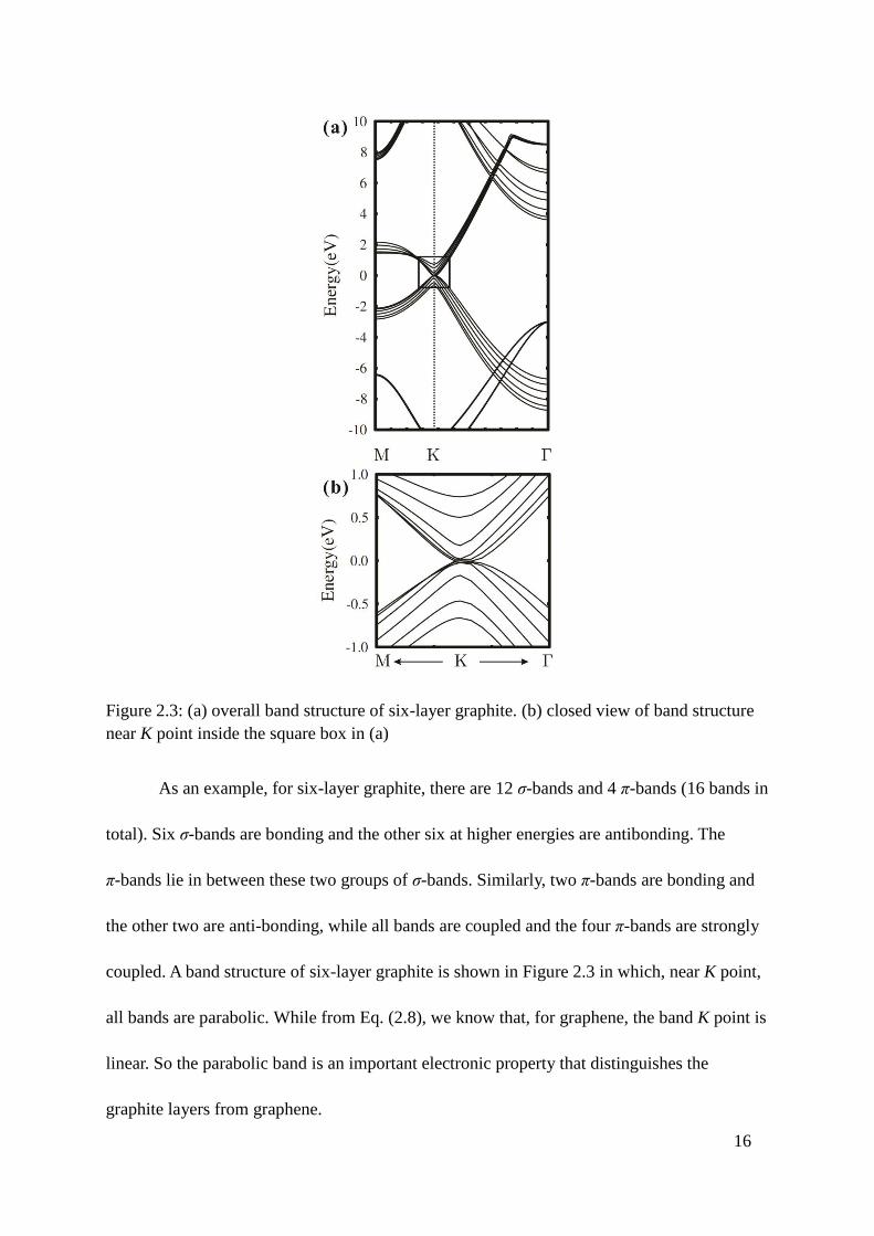
Figure 2.3: (a) overall band structure of six-layer graphite. (b) closed view of band structure
near K point inside the square box in (a)
As an example, for six-layer graphite, there are 12 σ-bands and 4 π-bands (16 bands in
total). Six σ-bands are bonding and the other six at higher energies are antibonding. The
π-bands lie in between these two groups of σ-bands. Similarly, two π-bands are bonding and
the other two are anti-bonding, while all bands are coupled and the four π-bands are strongly
coupled. A band structure of six-layer graphite is shown in Figure 2.3 in which, near K point,
all bands are parabolic. While from Eq. (2.8), we know that, for graphene, the band K point is
linear. So the parabolic band is an important electronic property that distinguishes the
graphite layers from graphene.
Page 24
17
In fact, this diference has been first theoretically predicted by P. Wallce in 1947. By
applying the traditionally tight binding approach to graphite lattice, and expending the E(k)
dispersion function near K point via Furious expansion, Wallace obtained the band structure
of graphite near the K point:
= 0 + 3𝛾 √3𝜋𝛾| − 𝑐|𝑎 − 3𝜋2𝛾 | − 𝑐|2𝑎2 (2.1 )
where kc is the coordinate of K point in reciprocal space. And the binding parameter 𝛾
can be thought of as the hopping energy between two nearest neighbor carbon atoms
(adjacent A and B atoms in the plane), and 𝛾 can be viewed as the hopping energy between
two A- site carbon atoms that are directly on top of each other from adjacent planes. To
obtain the band structure of single layer of graphite (or graphene), simply neglect the
parameter of interlayer hopping energy (𝛾 ), then only the linear term in Eq. (2.17) survives,
we have:
| − 0| ≈ √3𝜋𝛾| − 𝑐|𝑎 (2.18)
this is consistent with Eq. (2.8) which is derived directly from single layer graphene. This
shows how the band structure near K point transits from parabolic to linear as the graphite
layer is fully separated from the bulk. As we will see in the later discussion with our results,
as the graphite layer is gradually separated from the bulk, the linear characteristics of its band
dispersion occur, representing the transition from a layer of graphite to graphene.
Page 25
18
CHAPTER 3 SCANNING TUNNELING MICROSCOPY
3.1 Background
The scanning tunneling microscope (STM) was invented by G. Binnig and H. Rohrer
[77, 78, 79] at IBM in 1982 and awarded the Noble Prize in 1986. The invention of STM
provides a powerful tool to obtain structural and electronic information of a materials surface
on an atomic scale. For example, the first atomically resolved STM image resolved and
confirmed the Si(111) 7 × 7 surface reconstruction [80, 81] and identified Takayanagi’s
dimer-adatom stacking- fault model [82] as the correct Si(111) 7 × 7 surface structure. The
basic idea of STM is bringing an ultra-sharp metallic tip in close proximity (a few Å) to a
conducting sample surface. As a bias voltage is applied between tip and sample, due to the
tunneling effect of quantum mechanics, an electric current can flow from the sample to the tip
or reverse. The tunneling current exponentially depends on the tip-sample distance, resulting
in a high vertical resolution [83]. As the tip scans across the surface and detects the current, a
map of the surface can be generated with a lateral resolution in the order of atomic scale.
3.2 Electron tunneling
Inside the solid crystal, most of the electrons are bounded tightly to individual atomic
nuclei due to the electrostatic interaction from the nuclei. This is similar to the case of an
isolated single atom and these electrons are called core electrons. However, there are some
electrons which are moving far away from the nuclei and feel a relatively weak electrostatic
force. These electrons are called conduction electrons in a metal. They can be modeled as if
Page 26
19
they are moving in a nearly constant attractive potential in the nearly free electron
approximation. A large number of the electron energy levels interact with each other to form
the so called conduction band. The energy level of the most weakly bound electrons is called
the Fermi Energy (EF) level at which the electrons are held in the crystal by an energy barrier
of ~5 eV, this is called the work function of the crystal. In classical physics, these electrons
can never leave or escape from the crystal for they do not have enough energy to overcome
the potential barrier. In Quantum Mechanic, however, the electrons near Fermi level have
probability to penetrate or tunnel through the potential barrier. This results in the wave
function leaking out 𝜓(𝑥) = 𝜓(0)𝑒−2𝜅 near the conductive sample surface and the
metallic tip, where 𝜅 is called decay length. By placing them near each other, a finite square
well can be created, and the leaked out electron wave-function of the tip and sample overlap
each other. This overlap wave function leads to a tunneling current as the bias voltage is
applied.
In classical mechanics, the motion of an electron with energy E moving in a potential
U(x) is determined by the equation:
𝑝
2
2𝑚+ 𝑈(𝑥) = (3.1)
where m is the mass of the electron. In regions where E > U(x), the electron has a nonzero
momentum pz. According to classical mechanical, the electron does not have the ability to
penetrate into any region with E < U(x), or a potential barrier. In quantum mechanics, the
motion of an electron, however, is determined by a wave function ψ(z) that satisfies the
Schrodinger’s equation,
Page 27
20
ℏ2
2𝑚
𝑑2
𝑑𝑥2𝜓(𝑥) + 𝑈(𝑥)𝜓(𝑥) = 𝜓(𝑥) (3.2)
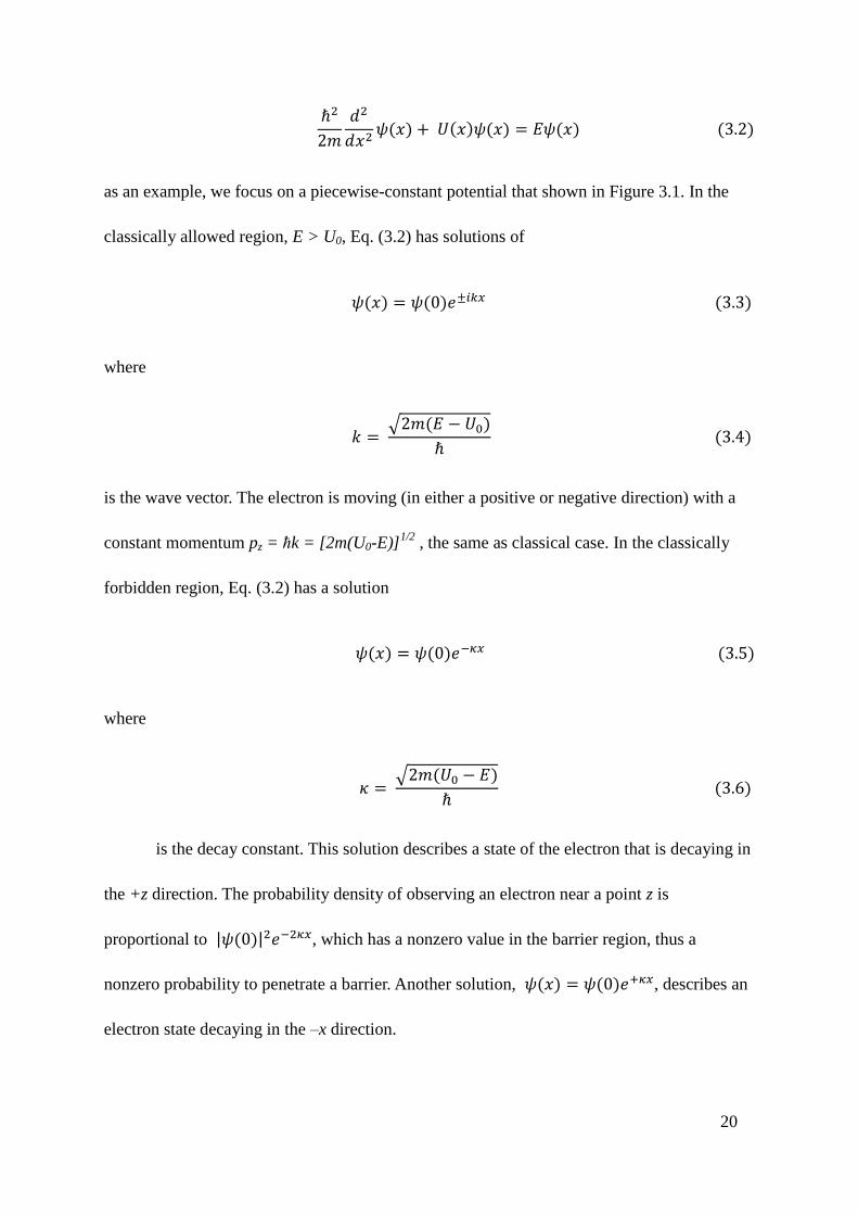
as an example, we focus on a piecewise-constant potential that shown in Figure 3.1. In the
classically allowed region, E > U0, Eq. (3.2) has solutions of
𝜓(𝑥) = 𝜓(0)𝑒 𝑖𝑘 (3.3)
where
= √2𝑚( − 𝑈0)
ℏ (3.4)
is the wave vector. The electron is moving (in either a positive or negative direction) with a
constant momentum pz = ћk = [2m(U0-E)]1/2
, the same as classical case. In the classically
forbidden region, Eq. (3.2) has a solution
𝜓(𝑥) = 𝜓(0)𝑒−𝜅 (3.5)
where
𝜅 = √2𝑚(𝑈0 − )
ℏ (3. )
is the decay constant. This solution describes a state of the electron that is decaying in
the +z direction. The probability density of observing an electron near a point z is
proportional to |𝜓(0)|2𝑒−2𝜅 , which has a nonzero value in the barrier region, thus a
nonzero probability to penetrate a barrier. Another solution, 𝜓(𝑥) = 𝜓(0)𝑒+𝜅 , describes an
electron state decaying in the –x direction.
Page 28
21
Figure 3.1: schematics of quantum mechanics tunneling model. It describes the quantum
mechanical phenomenon where a particle tunnels through a square barrier that it classically
impossible.
The principle of STM is based on the elementary tunneling model discussed above..
In general, the work function 𝜙 depends on both the material and the crystallographic
orientation of the surface. By neglecting the thermal excitation, the Fermi level, which is
essentially the total chemical potential for electrons, can be treated as the upper limit of the
occupied state in a metal. If we take the vacuum level as the reference energy level, we have
EF = −𝜙. In the following, for simplification, we assume that the work function of the tip
and the sample are equal. As a metal tip and a conducting sample are brought close to teach
other and a bias voltage V is applied between them, a net tunneling current occurs between
them. A quantum mechanics sample state 𝜓𝑛 with energy En lying between the interval from
EF -eV to EF has a high probability to tunneling into the tip. By assuming that the bias is
much smaller than the value of the work function, 𝑒𝑉 ≪ 𝜙, it can be concluded that energy
levels of all sample states of interest are very close to the Fermi level, 𝑛 ≈ −𝜙. The
Page 29
22
probability for an electron in the nth sample state to tunnel into the tip surface, x = s, is given
by
𝑃 ∝ |𝜓𝑛(0)|2𝑒−2𝜅𝑠 (3. )
where
𝜅 = √2𝑚𝜙
ℏ (3.8)
is the decaying constant of a sample state near the Fermi level inside the barrier region, and
𝜓𝑛(0) is the value of the wave function of nth state at the sample surface (at x=0). During
the experiment, the STM tip is scanning across the sample surface. During the scan, the
condition of the tip usually does not change. The tunneling current is directly proportional to
the number of states on the sample surface within the energy interval eV. This number is
determined by the local nature of the sample surface. And it is finite for metals while is very
small or zero for semiconductors and insulators. For semimetals, it is in between. The
tunneling current, therefore, should include all the sample states in the energy interval eV, and
it can be written as:
𝐼 ∝ ∑ |𝜓𝑛(0)|2𝑒−2𝜅𝑠
𝐸𝐹
𝐸𝑛=𝐸𝐹−𝑒𝑉
(3.9)
If the bias voltage V is small enough that the density of electronic states does not
change significantly within energy gap of eV, for convenience, the sum in Eq. (3.9) can be
written in terms of the local density of states (LDOS) at the Fermi level. At a location z and
energy E, the LDOS of the sample is defined by:
Page 30
23
𝜌𝑠(𝑥, ) ≡ 1
𝜖∑ |𝜓𝑛(𝑥)|2
𝐸𝐹
𝐸𝑛=𝐸𝐹−𝑒𝑉
(3.10)
for a sufficiently small 𝜖. The physical meaning of LDOS is the number of electrons per unit
volume per unit energy, at a given location in space and at a given energy. The probability
density for a specific state, |𝜓𝑛|2, satisfying the normalization condition: the integration of
this probability density over the entire space should be 1. As the volume increase, the
probability density |𝜓𝑛|2 of a single state decreases; but the number of states per unit energy
increases. The LDOS remains a constant. The surface LDOS near the Fermi level reveals of
whether the surface is metallic or insulating. By defining the LDOS of the sample surface, the
tunneling current can be written as:
𝐼 ∝ 𝑉𝜌𝑠(0, 𝐹)𝑒−2𝜅 ≈ 𝑉𝜌𝑠(0, 𝐹)𝑒−1.025√𝜙 (3.11)
The typical value of work function is 𝜙 = 4 𝑒𝑉, which gives a typical value of the
decay constant 𝜅 = √2𝑚𝜙/ℏ ≈ 1 Å-1
. According to Eq. (3.11), the current decays by
about 𝑒2 ≈ .4 times per Å in distance.
Simply put, scanning tunneling microscope can be viewed as a very sensitive
profilometer. At the atomic scale, the STM is actually mapping the surface profile of the
sample. While at an atomic scale the notion of surface topography is still unclear. One simple
assumption is that, at the atomic scale, STM is mapping the contour of the charge density of
the surface material which is essentially the surface topography at the atomic scale. The
dominant contribution to the tunneling current is from electrons near the Fermi level. All
electrons below the Fermi level contribute to the charge density. (Hence, the assumption that
Page 31
24
the topography produced by changes in the tunneling current is a contour of the charge
density may not be entirely correct.)
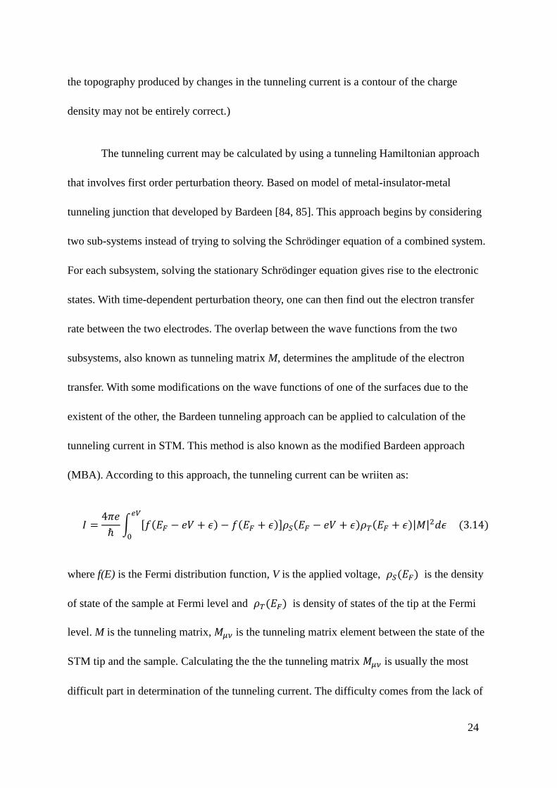
The tunneling current may be calculated by using a tunneling Hamiltonian approach
that involves first order perturbation theory. Based on model of metal-insulator-metal
tunneling junction that developed by Bardeen [84, 85]. This approach begins by considering
two sub-systems instead of trying to solving the Schrödinger equation of a combined system.
For each subsystem, solving the stationary Schrödinger equation gives rise to the electronic
states. With time-dependent perturbation theory, one can then find out the electron transfer
rate between the two electrodes. The overlap between the wave functions from the two
subsystems, also known as tunneling matrix M, determines the amplitude of the electron
transfer. With some modifications on the wave functions of one of the surfaces due to the
existent of the other, the Bardeen tunneling approach can be applied to calculation of the
tunneling current in STM. This method is also known as the modified Bardeen approach
(MBA). According to this approach, the tunneling current can be wriiten as:
𝐼 =4𝜋𝑒
ℏ∫ [ ( 𝐹 − 𝑒𝑉 + 𝜖) − ( 𝐹 + 𝜖)]𝜌𝑆( 𝐹 − 𝑒𝑉 + 𝜖)𝜌𝑇( 𝐹 + 𝜖)|𝑀|2𝑑𝜖
𝑒𝑉
0
(3.14)
where f(E) is the Fermi distribution function, V is the applied voltage, 𝜌𝑆( 𝐹) is the density
of state of the sample at Fermi level and 𝜌𝑇( 𝐹) is density of states of the tip at the Fermi
level. M is the tunneling matrix, 𝑀𝜇𝜈 is the tunneling matrix element between the state of the
STM tip and the sample. Calculating the the the tunneling matrix 𝑀𝜇𝜈 is usually the most
difficult part in determination of the tunneling current. The difficulty comes from the lack of
Page 32
25
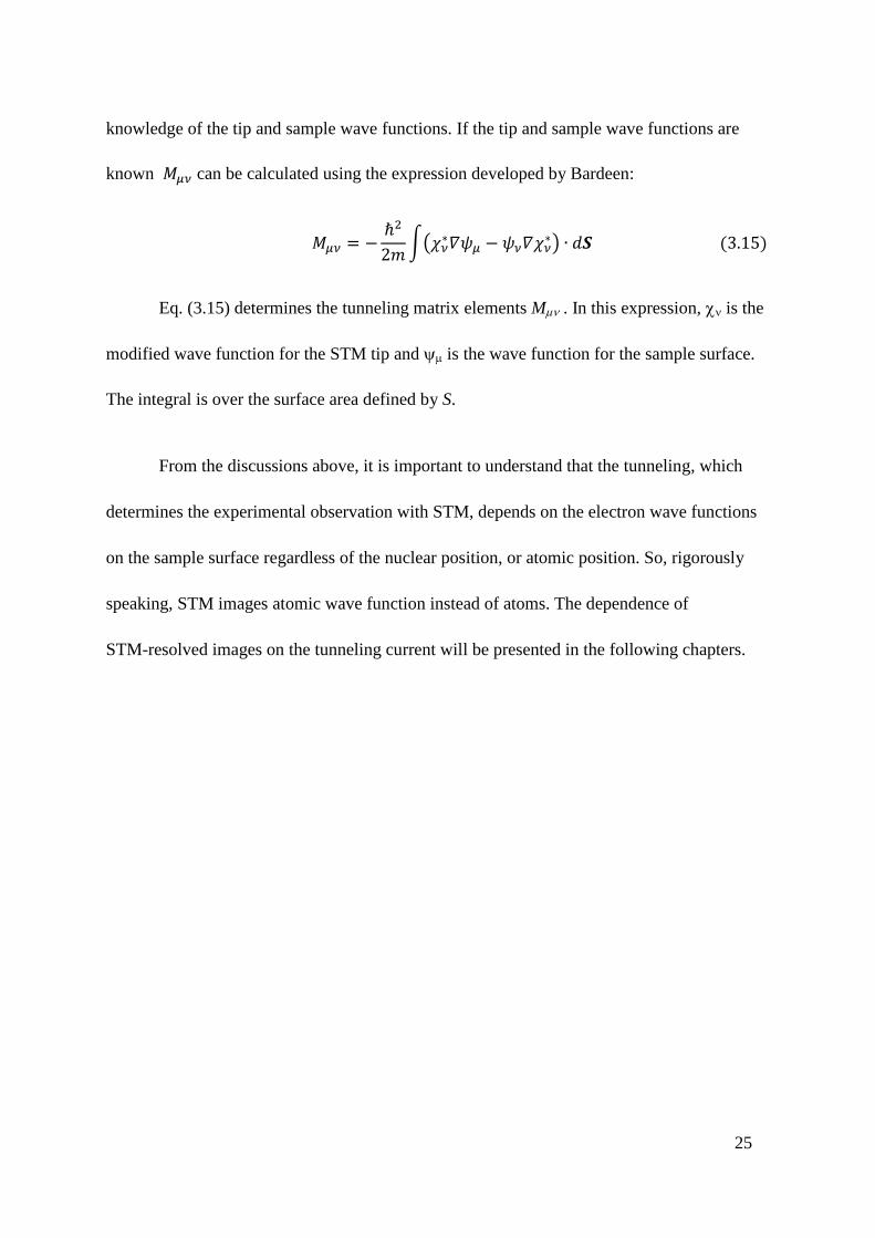
knowledge of the tip and sample wave functions. If the tip and sample wave functions are
known 𝑀𝜇𝜈 can be calculated using the expression developed by Bardeen:
𝑀𝜇𝜈 = −ℏ2
2𝑚∫(𝜒𝜈
∗𝛻𝜓𝜇 − 𝜓𝜈𝛻𝜒𝜈∗) ∙ 𝑑𝑺 (3.15)
Eq. (3.15) determines the tunneling matrix elements M . In this expression, is the
modified wave function for the STM tip and is the wave function for the sample surface.
The integral is over the surface area defined by S.
From the discussions above, it is important to understand that the tunneling, which
determines the experimental observation with STM, depends on the electron wave functions
on the sample surface regardless of the nuclear position, or atomic position. So, rigorously
speaking, STM images atomic wave function instead of atoms. The dependence of
STM-resolved images on the tunneling current will be presented in the following chapters.
Page 33
26
CHAPTER 4 EXPERIMENTAL DETAILS
4.1 STM tip making
The quality of the STM tip is crucial for obtaining atomic resolution STM image. In
order to effectively obtain atomic resolution, the probe tip must itself be on the atomic scale.
Ideally, it implies that the tip should end in exactly one atom. Reliably fabricating ultrasharp
metallic probes with a tip apex radius on the order of 10 nm has challenged researchers since
the debut of the field electron emission microscope by Müller in 1936, and has become even
more significant as field ion microscopy and scanning tunneling microscopy (STM) have
gained prominence and remained vital research techniques. Because the tip apex radius is
such a critically important attribute when attempting to image on the atomic scale,
experiments characterizing ultrasharp probes have primarily focused on the smallest scales,
employing scanning electron microscopy (SEM), which is capable of 100 000 ×
magnification. Such studies have established that ultrasharp metallic probes can, in fact, be
reliably manufactured by electrochemical etching, which is a simple, inexpensive, and widely
used technique [86]. For STM, tungsten wire is preferred because of its high conductivity,
mechanical strength, durability, and low cost [87]. Typically, electrochemical fabrication
methods involve submerging the tungsten wire and a conducting ring into an electrolytic
conducting solution, then applying a bias voltage of either dc [88] or ac [89] between them.
The resulting current between the ring and wire (mediated by the solution) drives a
reduction-oxidation reaction, which oxidizes the tungsten at the air/solution interface. This
basic scheme allows for many variations, each with its own advantages. A great deal of work
Page 34
27
has thus been devoted to developing optimal etching procedures for consistently and feasibly
producing high-quality tips [90].
One of the most recently developed tip fabrication techniques is to use tungsten wire
arranged horizontally under a high-magnification optical microscope, with the loop attached
to a micromanipulator for fine motion control [91]. The solution forms a lamella suspended in
the loop, which is moved back and forth over the tungsten wire while etching to create a tip
of the desired shape. This method, known as zone electropolishing, offers superior control
and precision, and even allows for re-etching a damaged or crashed STM tip. However, this
method does pose a problem in the final drop off step. It is necessary to thin a small section
near the end of the wire into a “neck” shape, and then precisely sever the wire while cleanly
separating the extra end piece. Finally, when the extra piece is removed, the etching must stop
immediately to avoid detrimental back etching, which quickly dulls the tip. The success of
this technique is dependent upon the patience, skill, and reaction time of the technician. To
address these potential difficulties, automatic etching systems have been constructed that
monitor the current flowing through the etchant and use feedback circuitry to terminate
power immediately upon completion of the tip etching (typical electrical cutoff time is on the
order of 10 ns). Unlike the micromanipulator method, in these systems the tungsten wire is
oriented vertically, and all components remain stationary during etching. Early designs
involved submerging the loop and wire in the electrolyte solution for the duration of the
etching, which provided unmatched simplicity. However, Klein and Schwitzgebel reported an
automatic method in 1997 that offered a far greater degree of control over the final tip shape
by using a lamella rather than submersion [92]. Nevertheless, cutoff circuits, in practice, often
Page 35
28
stop the etching too soon due to natural fluctuations in the current, making it necessary for
the operator to constantly monitor the process and occasionally restart it. In addition, the
change in current upon completion of the etching is occasionally too small to trigger the
cutoff circuit, resulting in the back-etching problem. A novel alternative is the mechanical or
gravity switch developed by Kulawik et al. in 2003, which utilizes two lamellas to break the
etching circuit as soon as the tip is finished etching [93]. In this setup, the current flows
through the end of the wire that is being etched off. Naturally, once etched through, the lower
part of the wire drops under the influence of gravity. This causes circuit breaking when the
wire breaks contact with the solution held in the upper lamella, providing a reliable cutoff
time of about 1–10 ms, depending on the thickness of the suspended fluid.
In this project, we developed a custom electrochemical etching procedure that
incorporates the best features of the common methods just discussed. Our double-lamella
system reliably produces ultrasharp tungsten probes capable of producing STM images with
atomic resolution, as demonstrated by testing the resulting tips on highly oriented pyrolytic
graphite (HOPG). STM tips were also manufactured using several other electrochemical
techniques and were similarly tested for quality by using them to image HOPG on the atomic
level. Furthermore, magnified optical images of the tips were acquired before they were
transferred into the STM chamber. A strong correlation was found to exist between a tip’s
cone angle and its ability to produce images with atomic resolution. We propose that this
observation is related to mechanical stability and can be used as a quick and economical test
to evaluate the probable quality of a tip, assuming it was etched by a typical electrochemical
method that has been shown by SEM to consistently yield sufficient sharpness at the apex.
Page 36
29
For comparison and to create additional tips with different characteristics, the popular
horizontal zone electropolishing method, the simple submersion method, a single-lamella
vertical method, and our double-lamella method were employed. The zone electropolishing
method was used most often. This technique requires ac voltage, high magnification, and
with a horizontal tungsten wire. In the submersion method, a single gold ring with a diameter
of a few centimeters was submerged into the NaOH solution, and a dc bias ranging from +3.0
to +6.0 V was applied to it. The tungsten wire was then lowered until only 2–3 mm remained
above the surface of the solution and 2 mm was below the surface. The etching rate along the
wire decreases quickly as the distance below the air/solution interface increases, resulting in
an atomically sharp tip. A differential cutoff circuit (Omicron Tip Etching Control Unit) was
used to automatically discontinue the bias and stop the etching when the current experienced
a sharp drop (i.e., when the lower part of the tungsten wire broke off and dropped into the
solution) [94]. The single-lamella technique was very similar to the submersion technique;
although the etching film is thinner and therefore produces a larger cone angle tip. A
differential cutoff circuit was again used to automatically discontinue the bias when the
bottom part of the wire fell.
Page 37
30
Figure 4.1: Photograph of the entire tip etching setup. The tip wire is held fixed at the focal
length of the microscope using a magnetic support. Two gold loops are mounted on a
micromanipulator with course x, y, and z control, which is located to the left. A hydraulic
fine z control is used to alter the etching position. A dc voltage is applied between the two
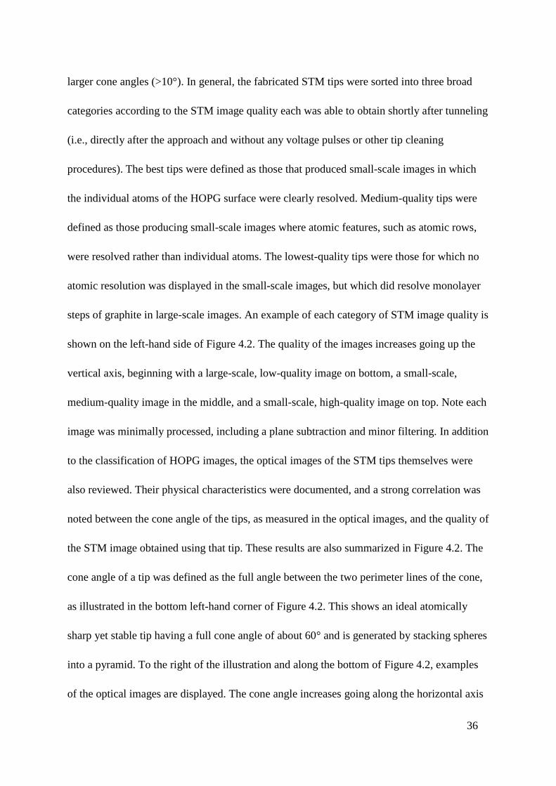
gold loops using a Keithley 2400 Sourcemeter shown to the right. (photo by Dejun Qi)
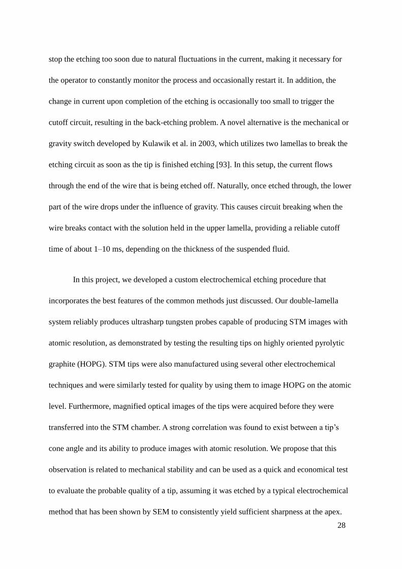
Over 200 STM tips were produced from 0.25 mm diameter polycrystalline tungsten
wire. Our STM tips were made by our optical microscope STM tip etching set up with double
lamella cut-off method, as shown in Figure 4.1. The etching process is powered by a Keithley
2400 Sourcemeter, as shown on the right-hand side of the photograph. This instrument
supplies a constant dc voltage throughout the etching process and also displays the current
flowing through the circuit. The eye pieces for the 30× magnification microscope can be seen
in the lower central region. Rather than being upright according to the original design, the
optical microscope is on its side (nearly horizontal), mounted on a custom support in a
Page 38
31
position that allows the tungsten wire to be oriented vertically during the etching progress.
The STM tip is held at a fixed position equal to the focal position of the microscope using a
magnetic stand that is positioned to the right of the microscope, as also shown in Figure 4.1.
The magnification provided by the microscope also facilitates careful regulation of the
thicknesses and positions of the lamellas. The position of the two loops is controlled using a
micromanipulator, which offers coarse adjustment in the x, y, and z directions, as well as a
fine hydraulic control for the z direction in order to maintain etching at the desired location
with minimal vibration. The micromanipulator can be seen to the left of the microscope near
the top of the photograph. The precision movement of the loops is necessary because zone
etching changes the shape of the wire, causing the top lamella (where etching occurs) to shift
and adhere to a slightly different site. In addition, the top lamella may pop several times
before the tip is finished etching, and requiring rewetting, followed by thinning. Note that it is
necessary to readjust the position of the loops to form around the same point on the wire as
previously.
Page 39
32
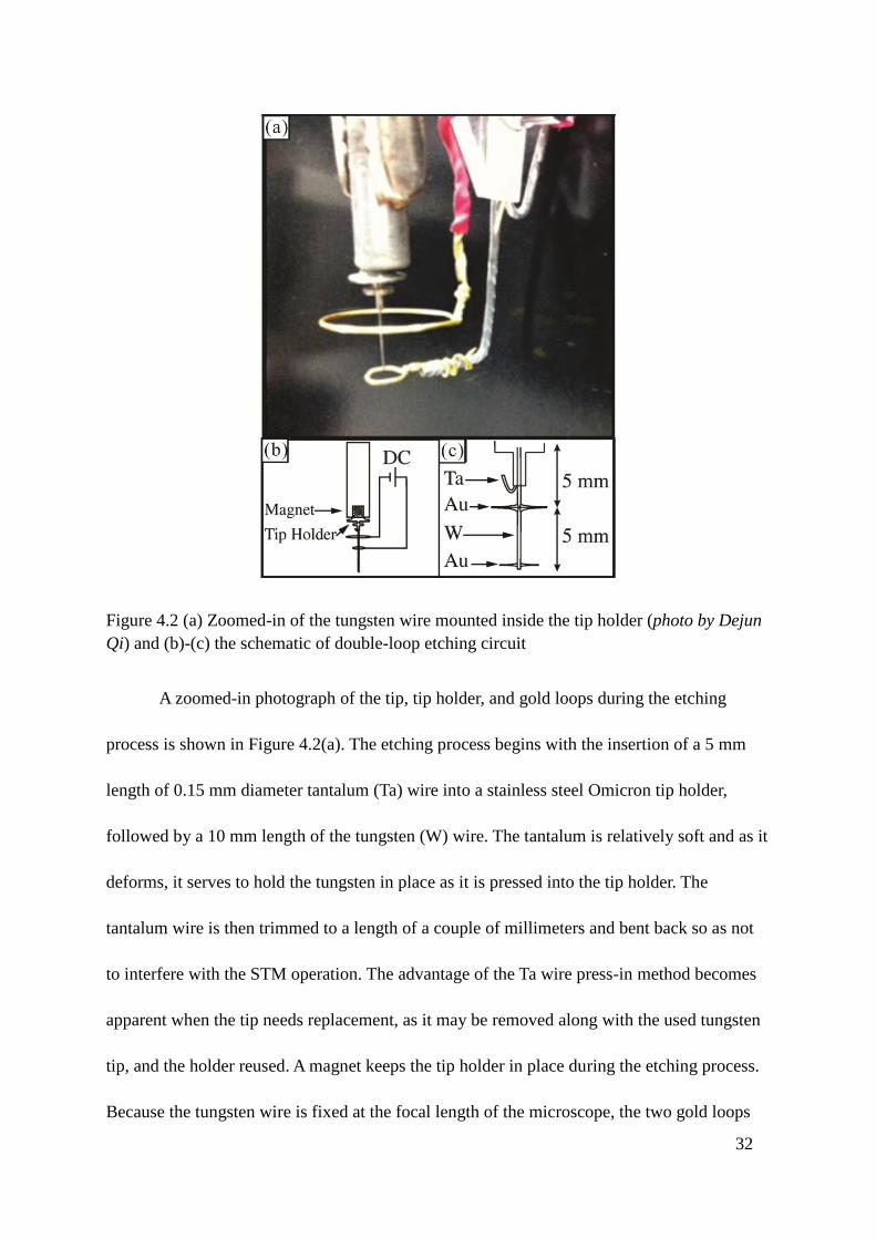
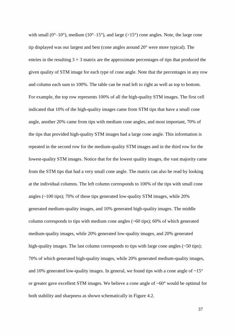
Figure 4.2 (a) Zoomed-in of the tungsten wire mounted inside the tip holder (photo by Dejun
Qi) and (b)-(c) the schematic of double-loop etching circuit
A zoomed-in photograph of the tip, tip holder, and gold loops during the etching
process is shown in Figure 4.2(a). The etching process begins with the insertion of a 5 mm
length of 0.15 mm diameter tantalum (Ta) wire into a stainless steel Omicron tip holder,
followed by a 10 mm length of the tungsten (W) wire. The tantalum is relatively soft and as it
deforms, it serves to hold the tungsten in place as it is pressed into the tip holder. The
tantalum wire is then trimmed to a length of a couple of millimeters and bent back so as not
to interfere with the STM operation. The advantage of the Ta wire press-in method becomes
apparent when the tip needs replacement, as it may be removed along with the used tungsten
tip, and the holder reused. A magnet keeps the tip holder in place during the etching process.
Because the tungsten wire is fixed at the focal length of the microscope, the two gold loops
Page 40
33
are raised up to surround the tungsten wire until the upper gold loop is within about 2–3 mm
of the end of the Omicron tip holder, the maximum length to avoid damage during transfer to
the scanner assembly inside the STM chamber after the tip is complete. The full etching
circuit and the mechanism behind the gravity switch are also illustrated in Figure 4.2(b). The
upper loop is attached to the grounded side of the dc supply, while the lower loop is attached
to the positive side (this moves the gas formation away from the etching site). When the wire
is etched away, the lower section of the wire drops due to gravity. This action results in the
electrical etching circuit being broken as soon as the falling wire separates from the etching
solution suspended in the upper loop (falling time is about 10 ms for a 1mm thick lamella).
The fall stops the etching process, even though the tip is still submerged in the etching
solution contained in the upper loop. This method works well and eliminates the need to rely
upon human intervention or a special response characteristic within the electrical circuit.
A magnified view of the tantalum wire, tungsten wire, and two gold loops is shown
schematically in Figure 4.2(c). The two gold rings are separated by about 5 mm and oriented
so that their faces are parallel and lie in horizontal planes. The top ring is 15 mm in diameter,
while the lower ring has a diameter of about 5 mm. A beaker containing a solution of 8 g
NaOH dissolved in 100 ml of de-ionized water is raised to briefly submerge the rings. When
the beaker is lowered, a thin film of the conducting solution is left suspended across each ring.
With the tungsten wire in place, a meniscus forms around the wire at each ring from the
suspended solutions as indicated in Figure 4.2(c). A thick meniscus was observed at the top
ring, where the wire was etched, resulting in a longer length of the tungsten wire etching tip,
which, in turn, creates a smaller cone angle. To achieve a thinner meniscus and therefore, a
Page 41
34
larger cone angle, some of the suspended solution can be carefully wiped away. Further, it is
important to monitor the meniscus and move it down the tapered section of the wire as it will
attempt to climb up the wire. Another, important factor is to make sure the tip is mounted
nearly vertical, so during the final etch step the lower piece of wire will not rotate and tear the
end of the W tip. During etching, the power supply was set to apply a dc bias of about 8 V
during the tip making process. A higher voltage results in faster etching. For our setup an 8 V
setting generated a potential difference of about 4.5 V between the tungsten wire and upper
gold loop. Note, as mentioned earlier, that the upper loop is held at a grounded side so that
the bubble formation happens at the lower loop. This stops the bubbles from interfering with
the etching process and also allows for a clear view of the tip throughout the etching. Also, as
the top wire is thinned the meniscus favors climbing up the W wire and it is important to
monitor this effect and move the loop down so the solution does not etch the wire above its
original starting location.
The completed STM tip is thoroughly rinsed with distilled water, then isopropanol,
and finally swirled in a concentrated HF solution for 30 seconds to remove any tungsten
oxides. The tips were then placed under an optical microscope and photographed under 100×,
500×, and 1000× magnification before being immediately transferred through a load-lock
into the STM chamber.
Page 42
35
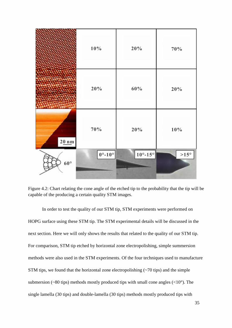
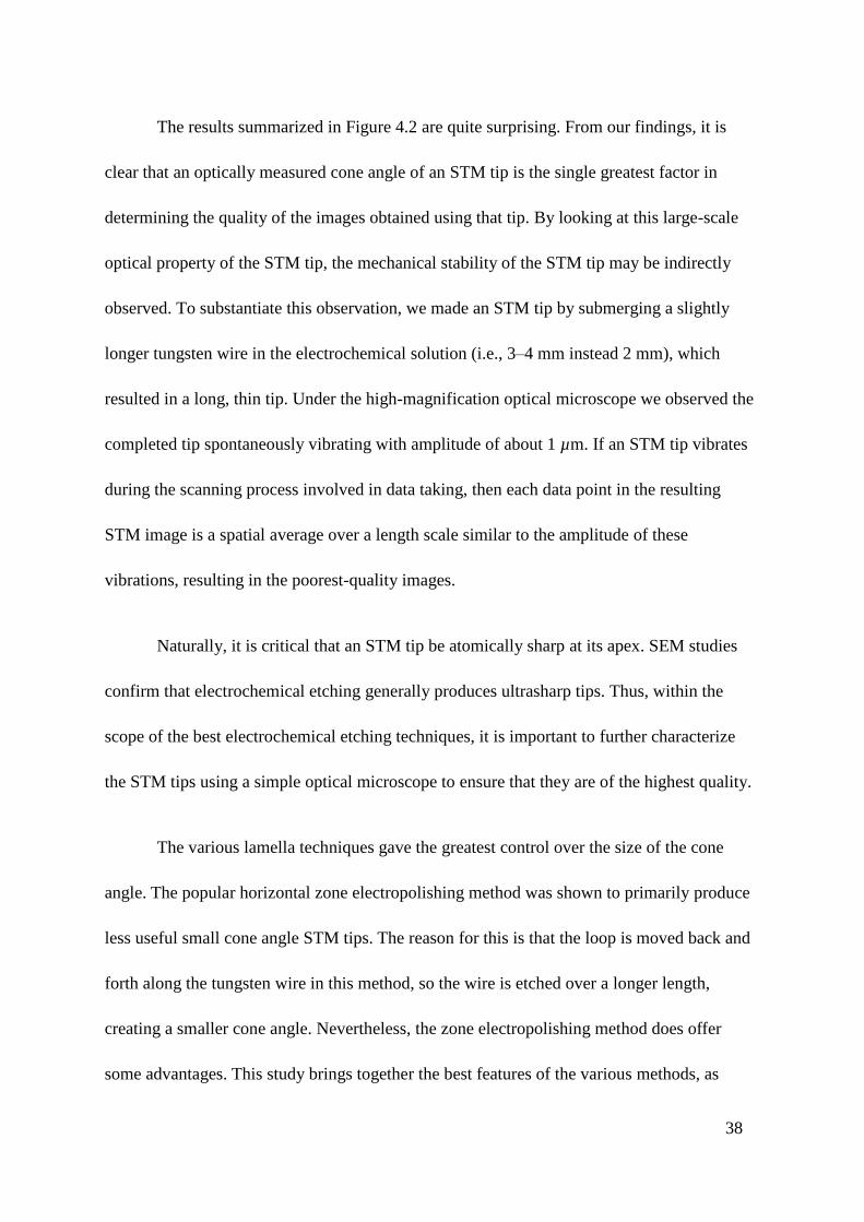
Figure 4.2: Chart relating the cone angle of the etched tip to the probability that the tip will be
capable of the producing a certain quality STM images.
In order to test the quality of our STM tip, STM experiments were performed on
HOPG surface using these STM tip. The STM experimental details will be discussed in the
next section. Here we will only shows the results that related to the quality of our STM tip.
For comparison, STM tip etched by horizontal zone electropolishing, simple summersion
methods were also used in the STM experiments. Of the four techniques used to manufacture
STM tips, we found that the horizontal zone electropolishing (~70 tips) and the simple
submersion (~80 tips) methods mostly produced tips with small cone angles (<10°). The
single lamella (30 tips) and double-lamella (30 tips) methods mostly produced tips with
Page 43
36
larger cone angles (>10°). In general, the fabricated STM tips were sorted into three broad
categories according to the STM image quality each was able to obtain shortly after tunneling
(i.e., directly after the approach and without any voltage pulses or other tip cleaning
procedures). The best tips were defined as those that produced small-scale images in which
the individual atoms of the HOPG surface were clearly resolved. Medium-quality tips were
defined as those producing small-scale images where atomic features, such as atomic rows,
were resolved rather than individual atoms. The lowest-quality tips were those for which no
atomic resolution was displayed in the small-scale images, but which did resolve monolayer
steps of graphite in large-scale images. An example of each category of STM image quality is
shown on the left-hand side of Figure 4.2. The quality of the images increases going up the
vertical axis, beginning with a large-scale, low-quality image on bottom, a small-scale,
medium-quality image in the middle, and a small-scale, high-quality image on top. Note each
image was minimally processed, including a plane subtraction and minor filtering. In addition
to the classification of HOPG images, the optical images of the STM tips themselves were
also reviewed. Their physical characteristics were documented, and a strong correlation was
noted between the cone angle of the tips, as measured in the optical images, and the quality of
the STM image obtained using that tip. These results are also summarized in Figure 4.2. The
cone angle of a tip was defined as the full angle between the two perimeter lines of the cone,
as illustrated in the bottom left-hand corner of Figure 4.2. This shows an ideal atomically
sharp yet stable tip having a full cone angle of about 60° and is generated by stacking spheres
into a pyramid. To the right of the illustration and along the bottom of Figure 4.2, examples
of the optical images are displayed. The cone angle increases going along the horizontal axis
Page 44
37
with small (0°–10°), medium (10°–15°), and large (>15°) cone angles. Note, the large cone
tip displayed was our largest and best (cone angles around 20° were more typical). The
entries in the resulting 3 × 3 matrix are the approximate percentages of tips that produced the
given quality of STM image for each type of cone angle. Note that the percentages in any row
and column each sum to 100%. The table can be read left to right as well as top to bottom.
For example, the top row represents 100% of all the high-quality STM images. The first cell
indicated that 10% of the high-quality images came from STM tips that have a small cone
angle, another 20% came from tips with medium cone angles, and most important, 70% of
the tips that provided high-quality STM images had a large cone angle. This information is
repeated in the second row for the medium-quality STM images and in the third row for the
lowest-quality STM images. Notice that for the lowest quality images, the vast majority came
from the STM tips that had a very small cone angle. The matrix can also be read by looking
at the individual columns. The left column corresponds to 100% of the tips with small cone
angles (~100 tips); 70% of these tips generated low-quality STM images, while 20%
generated medium-quality images, and 10% generated high-quality images. The middle
column corresponds to tips with medium cone angles (~60 tips); 60% of which generated
medium-quality images, while 20% generated low-quality images, and 20% generated
high-quality images. The last column corresponds to tips with large cone angles (~50 tips);
70% of which generated high-quality images, while 20% generated medium-quality images,
and 10% generated low-quality images. In general, we found tips with a cone angle of ~15°
or greater gave excellent STM images. We believe a cone angle of ~60° would be optimal for
both stability and sharpness as shown schematically in Figure 4.2.
Page 45
38
The results summarized in Figure 4.2 are quite surprising. From our findings, it is
clear that an optically measured cone angle of an STM tip is the single greatest factor in
determining the quality of the images obtained using that tip. By looking at this large-scale
optical property of the STM tip, the mechanical stability of the STM tip may be indirectly
observed. To substantiate this observation, we made an STM tip by submerging a slightly
longer tungsten wire in the electrochemical solution (i.e., 3–4 mm instead 2 mm), which
resulted in a long, thin tip. Under the high-magnification optical microscope we observed the
completed tip spontaneously vibrating with amplitude of about 1 µm. If an STM tip vibrates
during the scanning process involved in data taking, then each data point in the resulting
STM image is a spatial average over a length scale similar to the amplitude of these
vibrations, resulting in the poorest-quality images.
Naturally, it is critical that an STM tip be atomically sharp at its apex. SEM studies
confirm that electrochemical etching generally produces ultrasharp tips. Thus, within the
scope of the best electrochemical etching techniques, it is important to further characterize
the STM tips using a simple optical microscope to ensure that they are of the highest quality.
The various lamella techniques gave the greatest control over the size of the cone
angle. The popular horizontal zone electropolishing method was shown to primarily produce
less useful small cone angle STM tips. The reason for this is that the loop is moved back and
forth along the tungsten wire in this method, so the wire is etched over a longer length,
creating a smaller cone angle. Nevertheless, the zone electropolishing method does offer
some advantages. This study brings together the best features of the various methods, as
Page 46
39
shown in Figure 4.2, to consistently produce STM tips that yield a high percentage of
atomic-resolution images. One of the factors that most influenced our choices was the risk of
back etching, which was a primary reason for selecting the double-lamella gravity switch
approach. Additional improvements were made, however, within this framework. The second
important factor under consideration was our ability to control the shape of the tip, especially
its cone angle, as much as possible. Using a lamella to etch the wire gave a degree of control
over the final tip shape that was impossible to obtain in a submersion method. Having an
optical microscope focused on the tip combined with the manipulator’s control allowed us to
observe and modify the position of the lamella, making it possible to predict the cone angle
of the finished tip. A positive dc etching voltage was chosen to eliminate disruptive gas
formation at the etching site. The result of all of these choices was a reliable fabrication
method that generated, with a 70% success rate, STM tips capable of atomic resolution.
4.2 Samples preparation
The well fabricated STM tungsten tip was then gently rinsed with distilled water and
dipped into a concentrated hydrofluoric acid solution to remove surface oxide [95] before
being transferred into the STM chamber through a load lock. The STM experiments were
performed in an Omicron ultrahigh-vacuum (base pressure is 10-10
mbar), low-temperature
STM operated at room temperature. We have two samples: a 6 mm × 12 mm ×2 mm thick
piece of HOPG and freestanding graphene on a 2000-mesh, ultrafine TEM grid with a square
lattice of holes with side 2L = 7.5 μm and copper bar supports 5 μm wide, as shown in Figure
Page 47
40
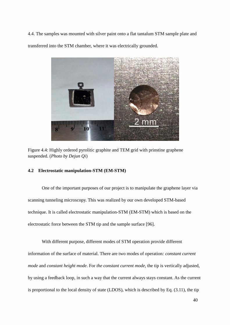
4.4. The samples was mounted with silver paint onto a flat tantalum STM sample plate and
transferred into the STM chamber, where it was electrically grounded.
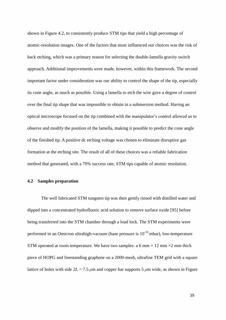
Figure 4.4: Highly ordered pyrolitic graphite and TEM grid with prinstine graphene
suspended. (Photo by Dejun Qi)
4.2 Electrostatic manipulation-STM (EM-STM)
One of the important purposes of our project is to manipulate the graphene layer via
scanning tunneling microscopy. This was realized by our own developed STM-based
technique. It is called electrostatic manipulation-STM (EM-STM) which is based on the
electrostatic force between the STM tip and the sample surface [96].
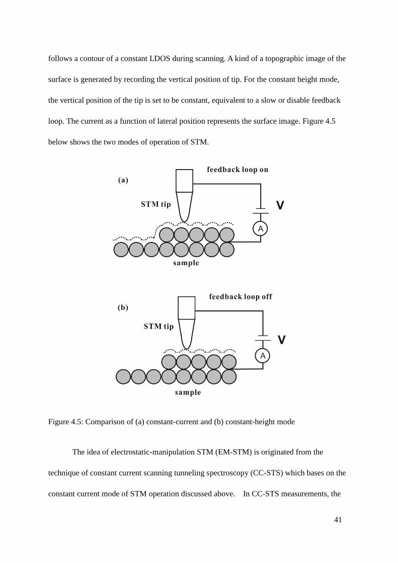
With different purpose, different modes of STM operation provide different
information of the surface of material. There are two modes of operation: constant current
mode and constant height mode. For the constant current mode, the tip is vertically adjusted,
by using a feedback loop, in such a way that the current always stays constant. As the current
is proportional to the local density of state (LDOS), which is described by Eq. (3.11), the tip
Page 48
41
follows a contour of a constant LDOS during scanning. A kind of a topographic image of the
surface is generated by recording the vertical position of tip. For the constant height mode,
the vertical position of the tip is set to be constant, equivalent to a slow or disable feedback
loop. The current as a function of lateral position represents the surface image. Figure 4.5
below shows the two modes of operation of STM.
Figure 4.5: Comparison of (a) constant-current and (b) constant-height mode
The idea of electrostatic-manipulation STM (EM-STM) is originated from the
technique of constant current scanning tunneling spectroscopy (CC-STS) which bases on the
constant current mode of STM operation discussed above. In CC-STS measurements, the
Page 49
42
tunneling current is held at constant value and the height of STM tip is measured as a
function of the tip bias. The EM-STM measurements performed were similar in principle to
CC-STS, wherein scanning is paused but the feedback loop controlling the tip’s vertical
motion remains operational. The STM tip bias is then varied, and one records the vertical
displacement required to maintain a constant tunneling current. Assuming the sample is
stationary, this process indirectly probes its LDOS. A second interaction is also taking place,
though, in which the tip bias induces an image charge in the grounded sample, resulting in an
electrostatic attraction that increases with the bias. We have found that in some materials,
such as graphite [97], this attraction can result in movement of the sample, convoluting and
often eclipsing any DOS measurement. In an EM-STM experiment, however, these
deformations are actually the subject of interest. By employing electrostatic forces created by
the STM tip, one may physically manipulate a surface and examine some of its mechanical
properties. Thus an EM-STM measurement involves recording the z-position of the tip as the
bias is varied at constant current, with the goal of controlled sample manipulation.
Page 50
43
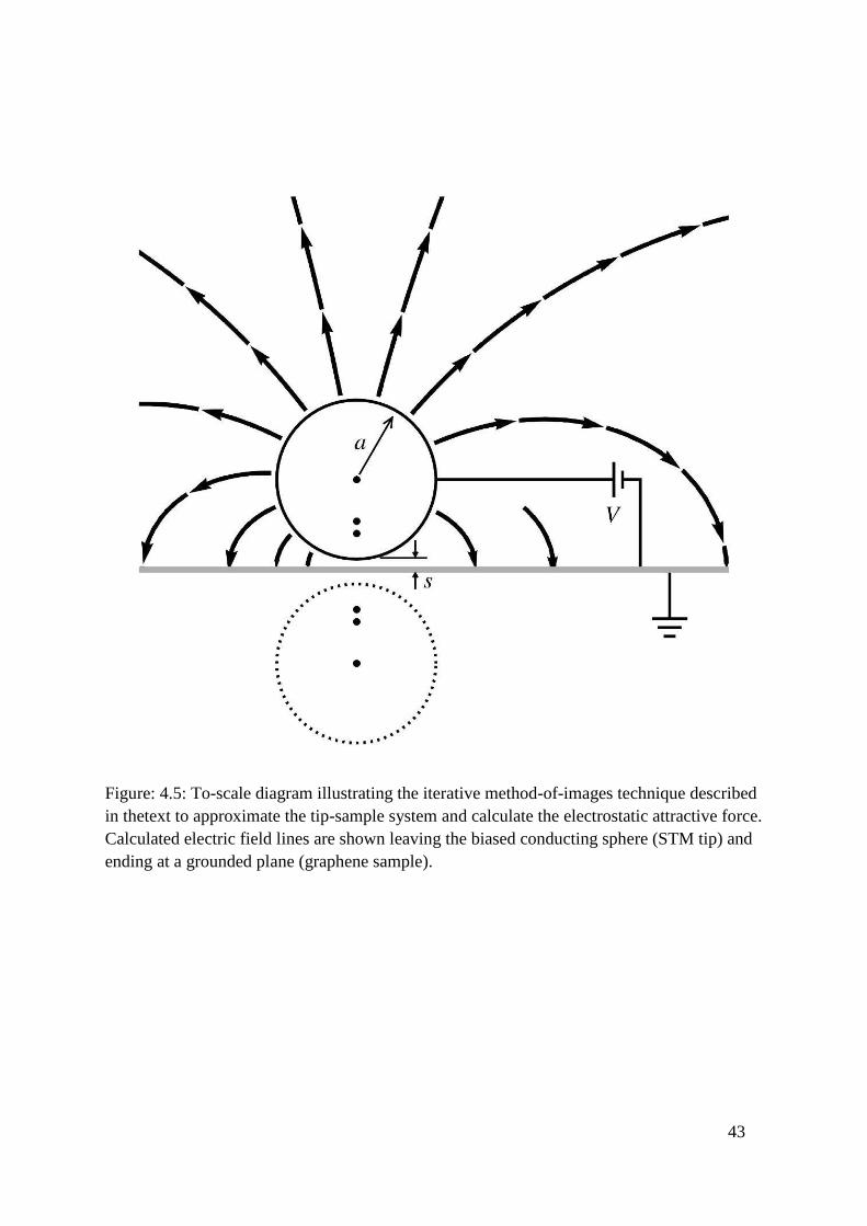
Figure: 4.5: To-scale diagram illustrating the iterative method-of-images technique described
in thetext to approximate the tip-sample system and calculate the electrostatic attractive force.
Calculated electric field lines are shown leaving the biased conducting sphere (STM tip) and
ending at a grounded plane (graphene sample).
Page 51
44
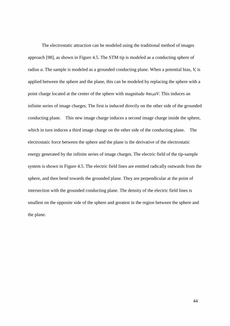
The electrostatic attraction can be modeled using the traditional method of images
approach [98], as shown in Figure 4.5. The STM tip is modeled as a conducting sphere of
radius a. The sample is modeled as a grounded conducting plane. When a potential bias, V, is
applied between the sphere and the plane, this can be modeled by replacing the sphere with a
point charge located at the center of the sphere with magnitude 4πε0aV. This induces an
infinite series of image charges. The first is induced directly on the other side of the grounded
conducting plane. This new image charge induces a second image charge inside the sphere,
which in turn induces a third image charge on the other side of the conducting plane. The
electrostatic force between the sphere and the plane is the derivative of the electrostatic
energy generated by the infinite series of image charges. The electric field of the tip-sample
system is shown in Figure 4.5. The electric field lines are emitted radically outwards from the
sphere, and then bend towards the grounded plane. They are perpendicular at the point of
intersection with the grounded conducting plane. The density of the electric field lines is
smallest on the opposite side of the sphere and greatest in the region between the sphere and
the plane.
Page 52
45
CHAPTER 5 GRAPHENE ON GRAPHITE
As described in Chapter 2, the Bernal (ABA) stacking of honeycomb carbon atom
sheets in bulk graphite gives rise to an inequivalence in charge density between atoms located
on two atomic sites—the A atoms on the surface which are directly on top of a carbon atoms
in the underlying layer and the B atoms that are located directly above the holes of a hexagon
rings in the underlying layer. Due to this unique stacking sequence of hexagonal carbon
layers, surface electronic charge has been partly pulled into the bulk, and hence, the STM
image of graphite surface normally shows a threefold-symmetric structure with a periodicity
of 2.46 Å.
Over the years, a number of explanations have been proposed for the unexpected
observation of true hexagonal atomic lattice structure on graphite surface via STM. These
explanations include tip artifacts [99], tip-induced surface elastic deformation [100, 101],
slipped surface configuration [102], interlayer coupling between asymmetric carbon atoms
[20, 27, 28, 103], change of current saturation that caused by variation of tip-sample distance
[104, 105], polarity of the bias voltage sensing different atomic sites [106], the formation of
charge density wave states [107] and the direct imaging of π states of alternate carbon–carbon
bonds [108] and so on. Regardless of the accuracy of these explanations, an important
conclusion can be drawn from this large amount of experiments and theories is that the local
density of states (LDOS) of each surface carbon atom is highly sensitive to its position
relative to the other atoms in the underlying layers. In this chapter, I will discuss our research
Page 53
46
of graphene on bulk graphite surface and show how the movement of surface graphite layer
can be generated and studied.
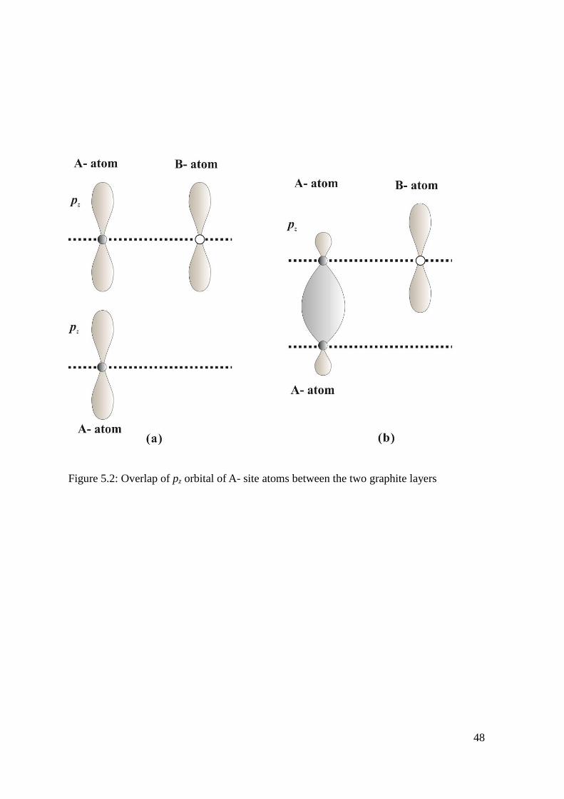
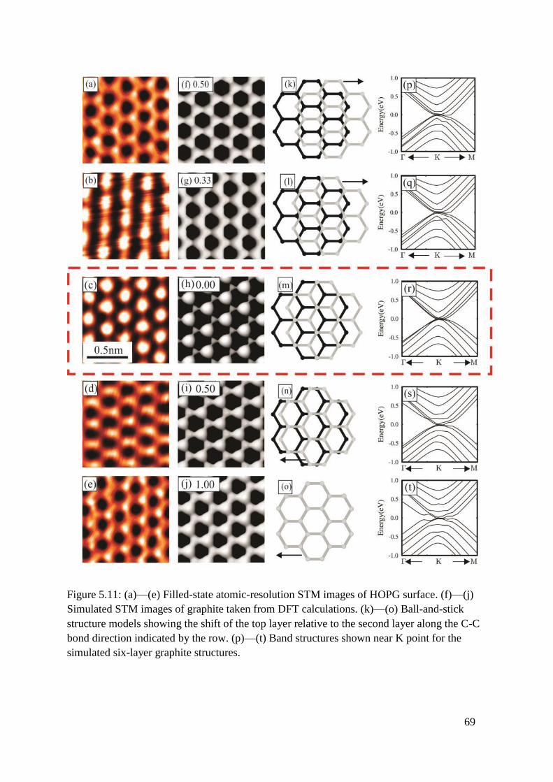
5.1 Surface morphology of graphite
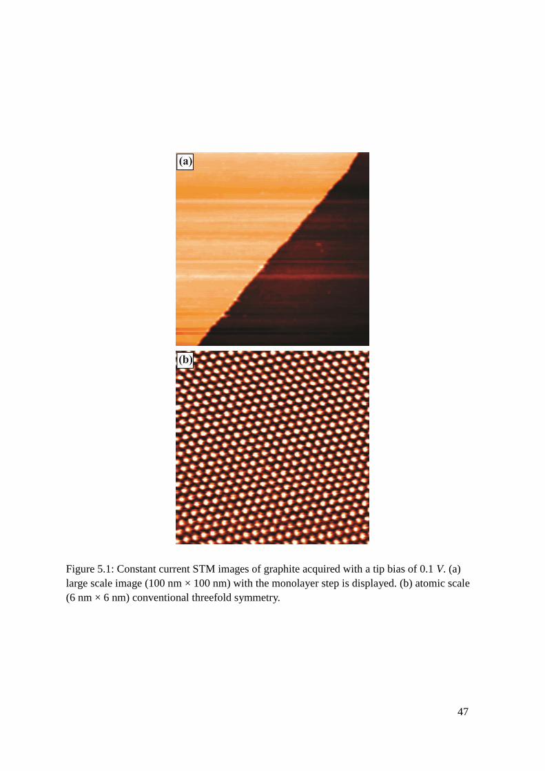
Two illustrative graphite STM images are displayed in Figure 5.1. Both have had
minimal image processing and are shown with the fast scan direction horizontal and with the
slow scan direction going from the bottom to the top. An STM image of the graphite surface
measuring 100 nm × 100 nm and with a monolayer step running diagonally across the surface
is shown in Figure 5.1(a). An atomic-resolution STM image measuring 6 nm × 6 nm showing
the traditional triangular symmetry lattice structure for graphite is shown in Figure 5.1(b).
This is the typical STM image for graphite and is relatively easy to obtain because only every
other carbon atom is detected. As we discussed before, in an ideal graphite crystal structure
with Bernal stacking pattern, the layers of carbon sheets stack together in a way that half of
the surface carbon atoms (A atoms) are directly above atoms in the lower layer, while the
other half (B atoms) are directly above hexagonal holes. The pz orbital of A-atoms of the
surface graphite layer overlaps with that of A-atoms in the lower layer, resulting in that the
electron charge density of the surface A-atom being pulled into the bulk, as illustrated in
Figure 5.2, from which we can see that the charge density of B- atoms on the surface is much
larger than that of A- atoms.
Page 54
47
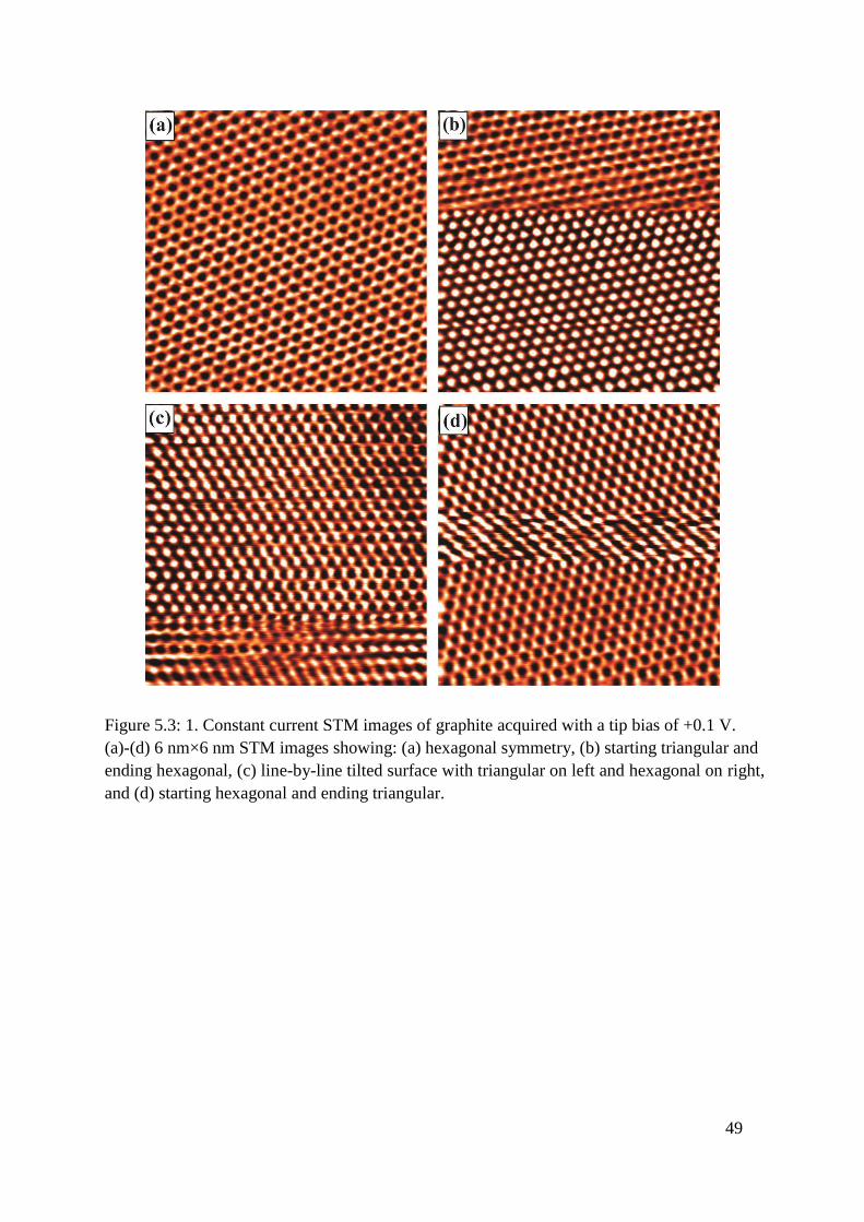
Figure 5.1: Constant current STM images of graphite acquired with a tip bias of 0.1 V. (a)
large scale image (100 nm × 100 nm) with the monolayer step is displayed. (b) atomic scale
(6 nm × 6 nm) conventional threefold symmetry.
Page 55
48
Figure 5.2: Overlap of pz orbital of A- site atoms between the two graphite layers
Page 56
49
Figure 5.3: 1. Constant current STM images of graphite acquired with a tip bias of +0.1 V.
(a)-(d) 6 nm×6 nm STM images showing: (a) hexagonal symmetry, (b) starting triangular and
ending hexagonal, (c) line-by-line tilted surface with triangular on left and hexagonal on right,
and (d) starting hexagonal and ending triangular.
Page 57
50
Sometimes while imaging graphite, all of the carbon atoms can be observed, resulting
in the hexagonal symmetry or honeycomb pattern as shown in Figure 5.3(a). This is the same
pattern one would observe when imaging isolated graphene (as we will see in the next
Chapter). Less common are STM images which show both triangular and hexagonal patterns
within a single image as shown in Figure 5.3(b). The beginning of this scan shows the
traditional graphite structure, while after about two-third of the scan the surface abruptly
switched to the hexagonal structure. Note, the subsequent STM image acquired (not shown)
was similar to graphene throughout. An even more interesting result is shown in Figure 5.3(c).
Here the triangular pattern occurs on the left side, while the hexagonal pattern occurs on the
right side. Note, this transformation occurs along the fast scan direction, line by-line
throughout the image acquisition process. Finally, the surface can also start out with a
hexagonal pattern and switch to the triangular pattern as shown in Figure 5.3(d). Here the last
three images of Figure 5.3 have been “flatten” so that each line of data has the same average
height.
The STM images in Figure 5.3 have been observed numerous times, over a long time
period, and with a plethora of STM tips. They are somewhat randomly occurring; however,
the frequency can be increased by increasing the setpoint current or reduce the bias voltage.
We believe the properties of the STM tip are not changing throughout these scans, but that the
local properties of the graphite sample are changing. For example, line-by-line one can see a
clear triangular atomic –resolution pattern along the left edge of Figure 5.3(c). Each atom
gets rescanned about 10 times (i.e., 400 data points per line with 400 lines per image) to piece
together the image of a single atom, and each row of atoms appears in the proper triangular
Page 58
51
position relative to the next row going up the scan. Simultaneously, and also line-by-line, a
clear hexagonal pattern is being observed on the right edge of Figure 5.3(c). It is not possible
to associate these changes with changes at the end of the STM tip.
Ideally, we would like to have these alterations occurring on the surface at our will
versus at random. The EM-STM measurement will allow this control.
Figure 5.4: EM-STM measurement on HOPG surface with bias changed from 0.1 to 1 V
A diagram with a typical EM-STM data set and some illustrations of how this
technique might appear on an atomic scale is shown in Figure 5.4. The EM-STM
Page 59
52
measurement was taken on graphite and is shown in Figure 5.4(a). Simultaneously, the
tunneling current was also measured, and the result is plotted in the inset diagram. Measuring
the tunneling current is critical to proving that the current remains at an approximately
constant value of 0.2 nA throughout the duration of the measurement. The EM-STM data
show that during the voltage sweep from 0.1 to 0.6 V the tip is held at its initial height with
little variation. An illustration showing the relative tip-sample position during this period is
shown in Figure 5.4(b). From 0.6 to 0.8 V the tip swiftly retracted by about 30 nm, at which
height it roughly stabilized. Notice the tunneling current remains essentially constant,
indicating that the sample follows the tip. The sudden movement of the tip suggests that the
top layer of graphite is being held in place by substrate until the electrostatic force of
attraction, which increases with voltage, becomes large enough to suddenly separate the
layers. A schematic of initial release due to the STM tip is illustrated in Figure 5.4(c). When
the voltage rises above 0.8 V, the top graphite layer is significantly lifted by the tip and fully
decoupled from the bulk locally as illustrated in Figure 5.4(d). Again, the measured tunneling
current serves as evidence that the sample surface must move with the tip. If it did not, the
current would exponentially fall to zero around 0.6 V. Note, traditional constant-height
(feed-back off) STS data was also acquired (not shown), but the current quickly saturated the
preamplifier at these higher voltage, consistent with the sample crashing into the stationary
STM tip.
The EM-STM technique significantly broadens the abilities of the STM, which is
already known for its superior ability to obtain atomic structural and local electronic
information for rigid samples. Now, if the sample is free to move or suspended, one can use
Page 60
53
EM-STM to gain insight into the local electrostatic and elastic properties. This could prove
valuable when considering chemically modified freestanding graphene, for example.
5.2 Altering surface morphology of graphite via EM-STM
The ability to physically alter the HOPG surface using EM-STM is demonstrated in
Figure 5.5. A series of 150 nm × 150 nm STM images all at the same location were taken
before, during and after EM-STM measurement, and the images are displayed in sequential
order in Figures 5.5(a) –3(e). As before, the slow scan direction of the STM tip proceeded
from bottom to top, and the images are colored such that the highest points are white (~2 nm
high) while the lowest points are black. A white strip approximately 20 nm wide is prominent
in Figure 5.5(a), indicating that a raised ribbon-like structure exists on the HOPG surface.
This image was taken prior to any EM-STM measurement. A darker strip, or trench, can also
be seen approximately 50 nm to the right of the white strip, with a protrusion in trench
serving as a reference point when presented in Figure. 5.5(b), an EM-STM measurement was
carried out shortly after the scan started. The STM tip was first positioned on the white strip
just above the in-progress scanning position, and the tip bias was increase from 0.1 to 10.0 V
at a constant tunneling current of 1.0 nA. Once the scan resumed, the white strip was found to
be displaced to the right, toward the protrusion. Surprisingly, after re-scanning the white strip
suddenly jump back to its original position. In the next scan we found that the lower
protrusion of the white strip had been displaced to the right as shown in Figure 5.5(c).
Page 61
54
Figure 5.5: Chronological series of about 150 nm × 150 nm filled-state STM images of one
location on graphite surface takenbefore, during, and after EM-STM measure with a tip bias
voltage of +0.1 V and a setpoint current of 1.0 nA.
Page 62
55
Figure 5.6: EM-STM measurement on the white strip. (b) Calculated electrostatic force
exerted by the STM tip on the graphite surface as a function of the tip height.
Now, however, this section is somewhat darker (it is likely a fold in the ribbon),
indicating that a permanent change has been introduced to the surface. To demonstrate this
ability again, a second EM-STM was taken during the subsequent scan shown in Figure
5.5(d). This resulted in a displacement of the upper portion of the white strip, this time away
from the trench. The next scan, taken immediately afterward and shown in Figure 5.5(e),
shows that a larger portion of the white strip is farther away from the trench, resulting in a
structure clearly distinct from that in Figure 5.2(a). A larger scale image of the same location
further reveals that a permanent change was made to the local region of the surface, as shown
in Figure 5.5(f). This sequence of images helps illustrate the size of the area that can be
impacted by an EM-STM measurement on graphite. The height of the STM tip versus bias
voltage, acquire during one of the two EM-STM measurements is shown in Figure 5.6(a),
with an inset showing that the tunneling current remains roughly constant at 1 nA. The
EM-STM measurement shows a continuous increase in the height of the STM tip with the
Page 63
56
increase of the bias voltage. The electrostatic force between the STM tip and the graphite
surface is calculated with the method of image model, as mention earlier in section 4.2. The
calculated electrostatic force versus voltage data was then combined with the experimental
EM-STM data in Figure 5.6(a) to produce the attractive electrostatic force as a function of tip
height shown in Figure 5.6(b). The force increase almost linearly with height to a maximum
force of about 4 nN. The area under the force vs. height curve yields an energy cost of about
230 eV being required to move the graphite strip.
5.3 Transition from graphite to graphene
A series of EM-STM measurements taken on the pristine graphite terrace is shown in
Figures 5.7(a)—(c). The set of data shows the range of results that can occur. Typically, the
height changes by a small amount when EM-STM is first applied to a given location [as
shown in Figure 5.7(a)]. Subsequent measurements in the same location can cause larger
movement to occur [as shown in Figure 5.7(c)]. In addition, we observed that reversal in the
movement can some time happen. The calculated electrostatic force as a function of applied
bias was used to convert the EM-STM data shown in Figs. 5.7(a)—(c) into the force versus
height curves shown in Figures 5.7(d)—(f), respectively. The same maximum force of about
0.4 nN is reached in each data set because the same voltage range was used for each data set.
Similar to before, the energy expended by the STM can be found from the area under each
curve.
Page 64
57
Figure 5.7: Characteristic EM-STM measurement on HOPG taken at various setpoint current
Page 65
58
Figure 5.8: (a)—(e) Filled-state atomic-resolution STM images of HOPG surface (f)—(k)
Similated STM images of graphite taken from DFT calculations. (l)—(q) Side views of the
simulated six-layer graphite structure shown with the top layer separated from the bulk by
different amounts. (r)—(w) Band structure near the K point for the six-layer graphite
structure as the top layer separates from the bulk.
Page 66
59
A series of high-magnification, atomic-resolution STM images of HOPG surface are
presented in Figures 5.8(a)—5.8(e). Going down the page, each image shows the gradual
transformation from full-triangular to full-hexagonal symmetry. We start with a typical STM
image of HOPG as shown in Figure 5.8(a). The bright white circles are arranged with perfect
triangular symmetry and represent the pz orbitals of the B-site carbon atoms which are above
the hexagonal holes in the second layer. For this image, the unit cell depicts only one atom.
Next, a very weakly visible A-site atom can be seen in Figure 5.8(b). An asymmetrical
hexagonal pattern is starting to appear in Figure 5.8(c). Two atoms are now apparent in the
unit cell but with a much larger charge density on one atom. A more balanced hexagonal
pattern is observed in Figure 5.8(d). The nearly perfect honeycomb pattern is observed in
Figure 5.8(e). Here both atoms in the unit cell possess nearly equal charge density,
resembling a typical STM image of graphene rather than graphite. This type of image on
HOPG is much less common than the triangular one, and in the past obtaining it has been
mostly a matter of chance. However, EM-STM provides a mechanism for directly
separating the surface layer from the bulk at will, effectively creating a section of graphene.
By systematically repeating the EM-STM measurement at successively higher voltages, one
can tune the displacement of the top layer. While this procedure does lift the layer, the top
layer is still attracted to graphite and thus quickly relaxes. Nevertheless, the likelihood of
observing the graphene hexagonal symmetry on graphite does greatly increase after
repeatedly performing EM-STM.
A full understanding of our experimental finding shown in Figures 5.8(a)—5.8(e) was
not possible until simulated STM images of HOPG were extracted from DFT calculation.
Page 67
60
These calculations were performed within the local-density approximation without modeling
the STM tip [109] and using projector augmented-wave potentials [110] as implemented in
the plane wave basis set VASP code [111]. The graphite was modeled as a six-layer Bernal
stack, using a 1 × 1 unit cell. A cutoff energy of 500 eV and a very large 219 × 219 × 1
Monkhorst-Park k-point meash was used to ensure proper sampling around the Dirac point.
Initially, the atoms were allowed to move until all forces were less than 0.1 eV/nm, resulting
in a carbon-carbon bond length of 0.142 nm and an interplanar separation of 0.334 nm. Then,
the top layer was moved away from the bulk in ten equal steps of size 0.015 nm, allowing
only in-plane relaxation at each step. For each configuration, a simulated constant-current
STM image was produced by integrating the local DOS from the Fermi level to 0.06 eV
below that point and choosing an appropriate isocontour surface. These parameters were
chosen to best replicate the experimental STM conditions.
Six simulated STM images taken from the DFT calculations are presented in Figures
5.8(f)—5.8(k). For each, the displacement of the top plane relative to its equilibrium position
is noted. Large spheres representing the electron density around the B-site atoms arranged in
a triangular pattern are shown in Figure 5.8(f). As discussed before, this is known to be due to
half of the top layer carbon atoms (A-site) forming a dimer bond with the carbon atom
directly underneath it in the plane below. This bonding is responsible for reducing the surface
charge density of these atoms. The much smaller and less bright adjacent features (shaped
like a small triangle) represent the electron density around the A-site atoms, but this is not
resolved in the experimental STM images. For net vertical displacements including 0.015 nm
up through 0.045 nm, the circles shrink while the triangles grow larger and more rounded. As
Page 68
61
we continue down the column to the 0.135 nm displacement, we see that the electron density
for each atom becomes essentially equivalent. Further displacements do not result in any
additional changes. The simulated images are in excellent agreement with the experimental
data.
The side views of the six-layer simulated structure with the top layer moving from a
net displacement of 0.00 to 0.135 nm are shown in Figures 5.8(l)—5.8(q). Notice that how
the charge density of the top layer becomes more separated from the bulk layers and becomes
more concentrated. More information about the electronic properties throughout the
displacement can be found in reciprocal space. The band structure near the K point for the
six-layer graphite structure (without any top layer displacement) is shown in Figure 5.8(r). As
expected, all the bands are parabolic. As the top layer moves vertically, the band structure
does not show any linear behavior at the Dirac point until Figures 5.8(v) and 5.8(w). This
marks the important electronic characteristic of graphene. Note there is an extra set of linear
bands coming from the odd number of layers remaining in the split-off graphite structure
[112]. After analysis of the band structure through the movement of the top layer, we estimate
around 0.090 nm the unique electronic properties of graphene are fully present. Namely, the
bands near K point are linear, and the total surface charge density has increased to nearly the
level of isolated graphene.
In addition to getting information about the real-space and reciprocal-space properties,
we also calculated the total energy of the system as a function of top-layer displacement, as
shown in Figure 5.9(a). The displacement is reported as a percentage of the strain ɛzz. The
Page 69
62
energy curve increases smoothly over the range sampled, and it transitions from positive to
negative curvature near a strain of 13.5% (or a displacement). This inflection point is
identified with an arrow. The calculated energy needed to fully separate one unit cell is found
to be approximately 50 meV. From our earlier estimates we found that the STM tip expended
50 eV to lift the top layer by 30 nm. Thus, we can now estimate that about 1000 unit cells
were separated during the lift. If the graphene was simply vertically lifted, a circular region
with radius of about 10 nm would be affected. Since this is similar to the height of the lifted
graphene, we believe that a much larger area may slide across the graphite surface.
Page 70
63
Figure 5.9: (a) DFT energy per unit cell as a function of vertical displacement of the top layer
of graphite. (b) Force as a function of displacement obtained by taking the derivative of the
energy with respect to displacement.
Page 71
64
Figure 5.10: (a) Normalized charge density on the A site and B siteas a function of
displacement. (b) Total charge density as a function of lattice position for both graphite and
graphene.
Page 72
65
Next, we can estimate the force required to separate the layers by taking the derivative
of the energy curve according to the Hellmann-Feynman theorem. This force (or uniaxial
stress σzz) is a result of the attractive force between the graphitic layers, which increases up to
the inflection point in the energy and subsequently decreases as shown in Figure 5.9(b). The
peak force required to separate the (1×1) layers is around 0.07 nN per unit cell. This is much
smaller than the estimated electrostatic force applied by the STM tip (4 nN), which is
consistent with the tip being able to lift up a large area of surface graphite.
The charge densities found on the A atom site (ρA) and the B atom (ρB) as a function
of layer separation is presented in Figure 5.10(a). The parameters have been normalized in
two ways. First, since the total electronic charge in top layer increased with the vertical
displacement, every charge density was divided by the total charge density at that point
ρtot=ρA + ρB. This ensures that we track only relative charge densities (ρA/ρtot and ρB/ρtot).
Second, a normalization was applied to the data for each atom so that the normalized
quantities N(ρA/ρtot) and N(ρB/ρtot) vary from 0 to 0.5 and from 0.5 to 1, respectively. Thus, at
zero displacement, N(ρA/ρtot) is a minimum and N(ρB/ρtot) is a maximum, consistent with the
STM images. Also, at the maximum displacement, the charge densities have equalized, also
as seen in the STM images. (Note that these values are independent the isovalue chosen for
the simulated STM images.) A key benefit of this normalized scheme is that N(ρB/ρtot)
represents a stepwise measurement of the decreasing interplanar coupling strength. If rescaled
from 0 to 1, this parameter can be thought of as the effective mass scaling parameter [113].
The other parameter N(ρA/ρtot) tracks the symmetry of the unit cell charge density. This
parameter is tending toward zero as the symmetry between A and B atom is being broken. In
Page 73
66
this sense, this parameter (if rescaled from 0 to 1) represents the order parameter for the
electronic reconstruction. The charge density profiles were also studied as a function of the
bias voltage. For lower bias voltage (i.e., states closer to the Dirac point) the charge densities
still began deviating from 50 % at a strain around 40%, but the change to 1 or 0 happened
more rapidly. This indicates that the states closer to the Fermi level are more sensitive to the
surrounding environment.
The total charge density in each plane of atoms of the six-layer slab of graphite is
shown in Figure 5.10(b). The six sets of double peaks represent the pz orbitals around each
atomic plane. The two end set of peaks are about half of the size of the bulk peaks.
Superimpose at the 0 nm position is the graphene charge density. Notice, the magnitude of the
graphene charge density is more than three times larger than graphite at the surface. This is
because, for graphite, the charge density at the surface is pulled into the bulk layers. Also,
notice the charge density for graphene is significantly wider than that for graphite. Overall,
the more massive charge density of graphene is also responsible for its high current carrying
capacity and thermal conductivity. Two simulated STM images (shown in side view) for the
surface of graphene and graphite are included as insert. The large charge density if graphene
pushes its surface (imaged by STM tip) further out into the vacuum.
In a broader context for our system, we are modeling the case where a normal force is
continuously applied to the graphene as it approaches graphite. The two system eventually
begin to interact, and the graphene transitions to a layer of graphite. Interestingly, if
pressure were applied still further, a second transition would occur from graphite to diamond
Page 74
67
[114], as has been recently verified experimentally using femtosecond laser pulses to achieve
the change [115]. However, what makes the graphene to graphite transition special is that it is
the only known system one can observe with atomic resolution about how the electron
acquires mass; or alternatively, how the electron loses mass and graphene generates the giant
charge density responsible for its high current carrying capacity and thermal conductivity.
5.4 Bernal (ABA) and rhombohedral (ABC) stacking
So far we have presented the EM-STM method and discussed the top graphite layer
being lifted vertically above the bulk. However, by scanning the STM tip, it is possible to
horizontally shift the top layer [116], also resulting in a graphene-like electron charge density
on the surface of graphite. In this section, we systematically study horizontal shifting, which
causes the transition between different stacking arrangements on the graphite surface. DFT
calculations are also completed to generated simulated STM images and analyze the
likelihood for each pathway.
Evidence for horizontal shifting of the top graphite layer along the carbon-carbon
bond axis is shown in Figure 5.11. Five characteristic atomic-resolution STM images are
shown in the leftmost column, and each shows a different symmetry. Anyone that has done
STM on HOPG has observed at one time or another STM images that are not typical outcome
shown in Figure 5.11(c). We have systematically cataloged all of these images into groups in
order to see a pattern. For example, in certain areas of the surface we can scan the tip along
the carbon-carbon bond axis direction, and the image changes from a triangular pattern to a
row-like pattern as shown in Figure 5.11(b). To ensure this was not due to the tip asymmetry
Page 75
68
but was due to the sample, this same tip was repositioned to other areas of the sample (a few
millimeters away), and the experiment was repeated. We found the effect was associated with
that specific region of the sample and did not follow the tip. Observation of a graphene-like
surface charge density on graphite is shown in Figure 5.11(a). STM images showing unequal
intensity between the two carbon sites along the scan direction are shown in Figures 5.11(d)
and 5.11(e).
Page 76
69
Figure 5.11: (a)—(e) Filled-state atomic-resolution STM images of HOPG surface. (f)—(j)
Simulated STM images of graphite taken from DFT calculations. (k)—(o) Ball-and-stick
structure models showing the shift of the top layer relative to the second layer along the C-C
bond direction indicated by the row. (p)—(t) Band structures shown near K point for the
simulated six-layer graphite structures.
Page 77
70
To gain insight into the origin of these results, simulated STM images were again
extracted from DFT calculations without modeling the STM tip. This time, instead of moving
the top layer vertically away from the bulk, it was slid along the surface. Specifically, the top
layer of graphite was shifted along C-C bond axis in units of a fraction of a bond length. The
shifting process is divided into six steps, shown in the form of a fraction of bond length [see
the top left corner of Figures 5.11(f)—5.11(j)]. The top view of simulated STM images are
shown in Figures 5.11(f)—5.11(j). With the top layer of the graphite in its equilibrium
position, a simulated STM image was generated and is shown in Figure 5.11(h), with a
ball-and-stick model for the top layer of graphite is shifted by half a bond length to the left,
the charge density of the B-site atom is still larger than that of the A-site atom, as shown in
Figure 5.11(i). The stacking pattern is shown with a ball-and-stick model in Figure 5.11(n). In
this pattern the B atom in the top layer has moved away from the center of the hexagon of the
lower layer and closer to the atom underneath. This increases interaction between them and
decreases the charge density of the B-site atom in the top plane. On the other hand, the A-site
atom has shifted farther from the atom underneath, resulting in a weaker coupling between
them which increases its charge density. After the top layer is shifted by one full bond length
along this same direction (left), the first two layers of graphite completely overlap, and all
carbon atoms in the top layer are interacting equally with all the carbon atoms in the lower
plane [see the model shown in Figure 5.11(o)]. A honeycomb structure is displayed in the
simulated STM image in Figure 5.11(j). Notice that the electron charge density of the A-site
atom is slightly different from the B-site atom. This is because a subtle effect coming from
the third layer. One pair of overlapping atoms is sitting directly above a carbon in the third
Page 78
71
layer, while the other pair of overlapping atoms is sitting directly above the hole at the center
of the hexagon in the third layer. Excellent agreement is again found between the
experimental STM data and the simulated STM data.
Next, in the computer model, the top layer of graphite was shifted 0.30 bond lengths
along the C-C bond-axis to the right this time, and another STM image was simulated as
shown in Figure 5.11(g). A row like structure similar to Figure 5.11(b) can be seen. The
stacking arrangement for this configuration is best observed in the model shown in Figure
5.11(l). This row like structure is attributed to the overlap between the carbon atoms in the
different layers. For a shift of 0.50 bond lengths, the charge density around all sites has
equalized, as seen in Figure 5.11(f). This gives the nice honeycomb structure and has
excellent agreement with the STM data shown in Figure 5.11(a). For the ball-and-stick model
shown in Figure 5.11(k), the top-layer carbon atoms are now exactly centered over the
benzene ring in the layer below. We define this symmetric configuration as the “no overlap”
structure since none of the carbon pz orbitals overlap with the ones in the plane below. Note,
even though the “AA” stacking also yields a graphene-like surface charge density, we believe
that the horizontal shift is not in this direction but is toward the no-overlap direction. Band
structure near the K point is shown as a function of horizontal displacement in Figures
5.11(p)—5.11(t). The most interesting results can be seen in the first and last diagrams.
Notice that the typical linear dispersion associated with graphene is not present in either case,
even though the simulated real-space STM images show the hexagonal symmetry of
graphene. This is because the top layer is still bonding with the surface, and a significant
amount of the top layer surface charge density is still spread out into the bulk.
Page 79
72
5.5 A path way from aba to abc stacking sequence
Evidence that the pathway between ABA and ABC is happening along the C-C
bond-axis direction and specifically toward the no-overlap structure is presented in Figure
5.12. A key STM image of HOPG surface is shown in Figure 5.12(a). This image has
“caught” the sudden transition from a graphite surface charge density to a graphene charge
density. On the left side of the image is the signature triangular lattice of graphite, while on
the right side is the distinct honeycomb structure of graphene. As mentioned earlier, previous
work has demonstrated graphene formation on graphite; however, it was manifested as a
continuous transition across the image. Our image is the result of a sudden jump, with the
slow scan direction oriented horizontally now (left to right), in which a discrete change has
occurred about two-third of the way through. Note that previous scans in this location showed
all graphite while the subsequent scans showed all graphene. From these data we cannot only
measure the vertical shift in the top layer, but we can also measure a horizontal shift as
discussed next.
Page 80
73
Figure 5.12: (a) STM image displayed with the slow scan direction going left to right. (b)
DFT energy/atom is plotted (squares) as a function of the top layer graphite horizontal shift.
Overlaid on top of the inset image in Figure 5.12(b) are two ball-and-stick models of
the graphene structure. The left-hand model is fit to the graphene image, while the right-hand
model is fit to the graphene image. The overlapping region of the two models shows the
Page 81
74
best-fit horizontal displacement that has occurred during the movement of the top layer. This
shows that the top layer of graphite was, in fact, shifted in the low energy direction
previously discussed and by an amount that corresponds to half a bond length. In the lower
part of Figure 5.12(b), the energy per carbon atom found from DFT while shifting to top layer
in ten equally spaced steps from ABA to ABC is shown. Note, at each step the top layer was
allowed to relax perpendicular to the surface to find the lowest energy pathway. The top layer
is shifted along the C-C bond axis direction but directly toward the no overlap configuration.
For this shift the ABC arrangement occurs after one bond length, and the no overlap situation
is at the halfway point. Notice the symmetric shape of the energy curve indicates that there is
no difference between the top surface layer shifting from ABA toward on overlap and from
ABC toward no overlap. However, when the top layer is shifted in the opposite direction,
starting with the ABA stack, the DFT energy per atom is very different as shown in Figure
5.13. When shifting in this direction, the top layer must move 2 bond lengths before reaching
ABC stacking and the halfway point is the well-known AA stacking configuration. Notice,
the barrier height for the no overlap direction is about 1.3 meV/atom in Figure 5.12(b), while
the opposite direction yields a barrier of about 17 meV/atom in Figure 5.13. Ball-and-stick
models illustrating the stacking arrangement for the ABA, halfway point, and ABC
configuration are also shown. Halfway through the shift shown in Figure 5.12(b) is the point
where the no overlap structure occurs between the top two layers [as more clearly illustrated
in Figure 5.11(k)] and a graphene-like surface charge density exists. Notice that the energy
curve has a relatively flat top at this point, which may result in a metastable state, allowing
Page 82
75
the STM tip to occasionally image this higher-energy configuration. In fact, we believe the
electrostatic attraction to the STM tip helps stabilize this configuration.
Figure 5.13: DFT energy/atom is plotted (circles) as a function of the top layer horizontal
shift
By analyzing the coordination number of the top layer atoms with the second layer
atoms, one can understand why the no overlap configuration should have the lowest energy
graphene-like surface charge density. In both the ABA and ABC stacks, half the atoms have 6
nearest neighbor (with the plane below) and half the atoms have only one 1, for an average
coordination number of 3.5. When in the no overlap configuration, the atoms each have 3
nearest neighbor, for an average coordination of 3. When in AA stacking configuration, the
atoms each have 1 nearest neighbor, for an average coordination of 1. Since the atoms prefer
to have a higher coordination number, the no overlap configuration energetically prefer over
the AA stacking structure.
Page 83
76
CHAPTER 6 GRAPHENE SUSPENDED ON TEM GRID
As the single graphite layer is totally decoupled from the bulk, its properties change
dramatically due to the 2-D quantum confinement of the charge carriers. Originally, the
theory did not support the existence of perfect 2-D crystal, while recent studies of the 2-D
crystal problem beyond the harmonic approximation [117, 118, 119] has demonstrated that
2-D membrane can be stabilized via the interaction and coupling between bending and
stretching long-wavelength phonons. The isolation of graphene has further proved this
conclusion. In order to understand the intrinsic properties of graphene and avoid the effect
that comes from any substrate, we performed our research of freestanding graphene over
holes. In this research the CVD graphene was transferred onto a 2000-mesh, ultrafine grid
with a square lattice of holes with side 2L = 7.5 μm and copper bar supports 5 μm wide [120].
Page 84
77
Figure 6.1: (Color online) (a) SEM image of 2000-mesh copper grid with transferred
graphene. (b) Constant-current scanning tunneling spectroscopy (CC-STS) data showing the
verticalmovement (d) of the STM tip vs applied bias voltage for three different set-point
currents. The bottom trace is graphene on copper data that has been offset for clarity. The
inset shows the measured current as a function of applied bias voltage. (c) Schematic of the
large-scale location of the STM tip below the freestanding graphene membrane with a low
(left) and a high voltage (right).
6.1 EM-STM measurement on freestanding graphene
A SEM image of the copper grid with the graphene membranes is shown in Figure
6.1(a). Notice that some of the holes in the copper mesh are fully covered by graphene, while
others are partially covered. We estimate that graphene covers more than 90% of the grid.
EM-STM data was acquired for both freestanding graphene and graphene on copper as
shown in Figure 6.1(b). The height (d) of the STM tip required to maintain a constant current
is shown, as the bias between the tip and the grounded sample is varied. The inset shows the
actual measured current versus voltage on a log scale. The constant current indicates that the
Page 85
78
sample and tip always maintain a close separation to sustain electron tunneling. For the
highest set-point current, the freestanding graphene membrane raises and follows the tip in
registry by about d = 30 nm when the voltage reaches 3 V. The result is almost fully
reversible as the graphene drops by about 35 nm when the voltage is ramped back down.
Graphene can be held at any height in between by simply changing the voltage accordingly.
The set-point current plays a similar role in the maximum displacement achieved. A tenfold
reduction in current reduces the maximum height achieved by the freestanding graphene by
about a factor of 2. Therefore, a combination of set-point current and bias (for fine tuning)
can be employed to set the height (d) of the graphene membrane at will. Note that, the Z-V
plot of graphene on graphite and freestanding graphene is similar in some extent but different
by the way of rising under the interaction of the STM tip. Graphene on graphite undergoes a
sudden jump due to the coupling with underlying bulk graphite while freestanding can be
lifted up more easily and controllable. The EM-STM technique is ideal for quantifying the
movement of the freestanding graphene since the voltage is incrementally changed in small
amounts (∼10 mV step size) and the acquisition waits for a long time (∼3 ms) so that the
feedback can stabilize before the current and new vertical position of the STM tip is recorded.
Page 86
79
Figure 6.2: (Color online) 6 nm × 6 nm filled-state (tip bias = +0.100 V, tunneling current =
1.0 nA) STM images of (a) graphene on copper. (b) Freestanding graphene. (c) Tip-induced
graphene on HOPG graphite with a tunneling current of 0.3 nA. Upper inset in (a)–(c): STM
images cut from the center. Lower inset in (a)–(c): Height cross-section line profiles taken
from the center. (d) Schematic illustrating the tip below a carbon atom (left) and below a hole
in the honeycomb lattice (right).
Constant-current STM images were also acquired from these samples. A STM image
of graphene on copper is displayed in Figure 6.2(a). The honeycomb structure is visible but
somewhat obscured by the harsh morphology of the copper substrate, which gives an overall
texture to the topography. The upper right-hand inset shows an atomic-resolution image from
Page 87
80
the central section of Figure 6.2(a) around a single honeycomb ring, magnified two times,
and displayed with a compressed color scale. Below the image is a height cross-section line
profile extracted from the center of the STM image, showing an atomic-scale corrugation (de)
of about 0.05 nm. The vertical scale is fixed at 1 nm for all the line profiles for easy
comparison. A STM image of the freestanding graphene is displayed in Figure 6.2(b). The
honeycomb structure is still visible but much less distinct due to the lateral movement of the
freestanding graphene membrane (described further below). This graphene image also shows
an overall curvature to the topography. Here it is highest and nearly constant along the
diagonal line from the lower left-hand side to the upper right-hand side. The most remarkable
feature of this data is that the underlying atomic lattice is still visible even with an overall
black-to-white color scale of 4 nm. The inset shows the local atomic structure with apparent
distortions. The atomic lattice is visible because the height change (d) across the honeycomb
is a full nanometer (see line profile below image), 20 times greater than the expected
electronic corrugation (de) for graphene on a substrate. For comparison, a high-quality STM
image of graphene on graphite [121] is presented in Figure 6.2(c). From the line profile
below the image, the corrugation amplitude is again about 20 times smaller than that of the
freestanding graphene membrane. Note the hexagons in these STM images confirm that it is
single-layer graphene.
6.2 Fluctuation of the attractive force
In this section, we present a number of theoretical results which point to the
significance of the controlled creation of strain fields (i.e., elastic distortions) on graphene by
Page 88
81
EM-STM. Given that the tip interacts with the membrane at a point, we first took a small
graphene supercell with 50 atoms, width 2L ≈2 nm, and pulled the center atom, leaving the
corner atoms fixed. The central atom was gradually displaced an amount d, through a series
of 0.03-nm increments, up to a maximum perpendicular displacement of 0.30 nm from the
plane. At each displacement, the other atoms were allowed to relax to the energy minimum.
The atomic relaxation was carried within the local density approximation to density
functional theory (DFT) with projector augmented-wave potentials as implemented in the
plane-wave basis set VASP code. The restoring elastic force was obtained from the
Hellman-Feynmann theorem as the derivative of the energy data versus displacement and
displayed in Figure 6.3(a) [the inset shows a schematic of the supercell in a side view, while
Figure 6.3(b) shows the strained model in a tilted view]. The linear fit shown for distortions
with d / L<0.1 produced a spring constant of about 20 nN per nm. With the reported
maximum vertical distortion, and assuming the STM tip was near the center of the suspended
membrane, we obtained a d / L = (35 nm)/(3.25 μm)∼0.01 from our data in Figure 6.1, well
within the linear region. This normalized displacement yields a restoring force of about 0.25
nN from Figure 6.3(a).
Page 89
82
Figure 6.3: (a) Restoring force of graphene calculated from DFT vs normalized displacement,
with a linear fit completed over the range from 0 to 0.1. (b) Atomic model used in the DFT
calculations shown in a tilted view. (c) Force on a unit charge held 0.1 nm above the surface
as it is moved parallel to the surface and along a line from the center of the honeycomb to the
nearest carbon atom. A maximum force occurs over the carbon atom. (d) 5-nm radial average
of the pseudomagnetic field underneath the STM tip vs normalized displacement.
We next estimated the attractive force between the STM tip and the graphene
membrane with a simple calculation in which we computed the charge rearrangement in
graphene needed to screen a unit point charge placed 0.1 nm above the graphene plane, using
the self-consistent Hückel method. We used a 20 nm × 20 nm square patch of graphene
containing more than 15 000 π electrons for this purpose. The Coulomb force was computed
from the self-consistent charge distribution. The van der Waals contributions were not
considered in our calculation, because the charge accumulation component of the attractive
Page 90
83
force was sufficient to provide us with a qualitative picture with good insight into the origins
of the atomic-scale corrugation.
Indeed, the electrostatic force varies periodically across graphene as shown in Figure
6.3(c). Moving parallel to the graphene surface along a straight line toward one of the nearest
carbon atoms, the force oscillates between a minimum (0.15 nN) when the tip is directly
above a hole and a maximum (0.25 nN) directly above an atom. Thus, the attractive
electrostatic force between the tip and the graphene oscillates in perfect registry with
graphene’s atomic spacing. When the test charge was directly above a point halfway between
a hole and an atom, a lateral force was found to exist (not shown). The magnitude of this
lateral force is significant, at more than 10% of the vertical force. It draws the graphene sheet
sideways, causing the STM images of freestanding graphene to blur. Given that the force is
not constant during the scan, the STM tip must retract or approach the graphene membrane as
it scans the surface. The freestanding graphene follows the tip, as described previously; hence,
the atomic-scale corrugation (d) is much larger than that observed when graphene is on a
substrate (de).
Knowing from our experimental data and our DFT calculation that the membrane
strain is within the linear region, we used the analytical expressions for the deformation of a
membrane from the work of W. H. Duan. et. al., along with the expressions for the
pseudomagnetic field of F. Guinea, et al.’s work, and the deformation potential calculated by
H. Suzuura, et. al.[122], to estimate the pseudomagnetic field created by the induced strain
(d/L) in our setup. Given that d/L is small, in our calculation, we further assumed a circular
Page 91
84
profile at the edges of the graphene membrane where it contacted the copper. As a result, the
pseudomagnetic field has the following form: B(r,θ) = |B(r)|cos(3θ)]. We plotted the radial
average of |B(r)| between r =0 and 5 nmversus normalized displacement at r = 0 in Figure
6.3(d). For a normalized displacement consistent with our results (d/L = 0.01), the |B(r)| is
about 25 T beneath the STM tip. Historically, EM-STM data such as that shown in Figure
6.1(b) was used to measure the local work function φ using the following formula: φ (eV) =
0.95[Δ ln V/Δd (A° )]2, where V is the bias voltage and d is the tip height [123]. Applying this
formula to our graphene on copper data yielded a work function of about 1 eV, which was
smaller than the expected value of about 4 eV, but reasonable for STS [124, 125]. Applying
this formula to our freestanding graphene data, we found an “effective work function” of
about 10 meV, or 100 times smaller, but here the graphene membrane is free to move and
follows the retracting tip. The increased bias voltage increases the electrostatic force on the
freestanding graphene membrane, causing it to move toward the tip. To maintain a constant
current, the tip pulls away from the approaching graphene membrane. The membrane
continues to chase the tip until an elastic restoring force grows and eventually equals the
electrostatic force, as shown in the right-hand side of Figure 6.1(c). However, because there
is a random offset in the height of a few nanometers in the EM-STM data shown in Fig.
6.1(b), this may be evidence of different large-scale, low-energy configurations, or ripple
textures, of the graphene membrane [126]. This may also be the root cause of the two
different linear regions in the spectra. The first linear region is soft due to removing ripples
and the second region is hard due to straining the lattice. In this way, the EM-STM
measurement on freestanding graphene is a tool by which we can learn about the elastic
Page 92
85
properties and the induced electronic properties of freestanding graphene. It is also interesting
that for a fixed bias voltage (e.g., 3 V), the height d increases as the current set point
increases, counter to tunneling theory but consistent with our electrostatic attraction model.
Similar to the STS data, the STM data shown in Figure 6.2(b) has two features that contribute
to its atomic corrugation amplitude (d), one electronic (de), and the other elastic (u). The
electronic component is caused by the spatial variation in the electronic density of states,
which is normally observed with STM. For graphene on a substrate, this electronic height
change (de) is known experimentally and theoretically to be at most 0.05 nm. The elastic
component is caused by the local elastic distortion for the freestanding graphene. In a related
point, evidence for elastic distortions in graphite has been previously reported. To illustrate,
as the STM tip is brought into tunneling below a carbon atom, the freestanding graphene is
attracted to the tip by the electrostatic image force and moves toward it (similar to our earlier
discussion). The feedback circuitry retracts the tip until a stable equilibrium is achieved, as
illustrated in the left-hand side of Figure 6.2(d). Next, as the tip scans away from the atom
and moves toward the center of the hexagon, the electrostatic force decreases. Consequently,
the elastic restoring force causes the graphene sheet to retract away from the tip. The
feedback circuit prompts the tip to chase the graphene until the new equilibrium
configuration is reach, as illustrated in the right-hand side of Figure 6.2(d). This repetitive,
dynamic, and interactive process is in perfect registry with the electronic corrugation. This
study demonstrates that STM can be used to probe and induce a controllable strain on
freestanding graphene membranes. These findings lay the groundwork for using local probes
to study and manipulate the electrostatic/pseudomagnetic/mechanical interactions in a model
Page 93
86
environment. For example, it may be possible to study local defects, such as vacancies or
dopants, and their role in modifying the elastic and electronic properties of the membrane
using EM-STM.
Page 94
87
CHAPTER 7 SUMMARY AND CONCLUSION
In summary, this dissertation presents my studies of the elastic and electronic
properties of graphene on graphite and suspended graphene on a TEM grid via scanning
tunneling microscopy.
In the experimental part, high quality metallic probe tips were fabricated for the STM
experiments. We developed a double-lamella method for manufacturing STM tips
electrochemically. The double-lamella method that offers excellent control over the tip’s
shape and consistently produces ultrasharp probes capable of atomic-resolution STM images.
The setup has the tungsten wire oriented vertically while under optical magnification and
uses a manipulator to tune the process as it evolves. The resulting tips were photographed
under 1000× magnification and then used to acquire STM images of HOPG in order to
determine their overall quality. A strong positive correlation exists between the cone angle of
a tip, as determined by the optical images, and the chance that the tip will be capable of
atomically resolved STM images. Larger cone angle tips are more likely to provide better
STM images, as a result of their greater mechanical stability. Optical imaging of the tips can
be used to accurately predict their quality, making it an easy and inexpensive tool for
evaluating electrochemically etched tips prior to STM imaging.
In the research of graphene on bulk graphite, a possibility for learning something
useful about graphene’s electronic properties as well as for general STM imaging and
manipulation has been shown. Graphite has a series of advantages, such as low cost, flat,
conductive, easy to be cleaved for preparing atomically flat surface, and easy to image the
Page 95
88
atomic scale by STM. It is, therefore, one of the most commonly used substrates for STM
experiments. The reason why it is so easy to image is because the atomic corrugation
measured in a typical STM experiment is on the order of several angstroms, which is
anomalously large. The reason for that is the weak interlayer coupling and the strength of the
interaction between the STM probe tip and the surface graphene layer which causes it to
move (either vertically or horizontally) under the tip, as well as the likelyhood for the tip to
pull up flakes of graphite. We have demonstrated, in chapter 5, the ability to vertically raise
and horizontally shift of the surface graphite layer. This is the key to unravelling the complex
atomic patterns of this otherwise simple-seeming surface is related to the surface charge
reconstruction.
This was realized by using the so called electrostatic-manipulation-STM technique of
our own development which is based on the electrostatic force between the tip and sample
surface. Our new EM-STM technique significantly broadens the abilities of the STM
technique. STM is already known for its superior ability to obtain atomic structural and local
electronic information for rigid samples. Now, if the sample is free to move or suspended,
one can use EM-STM to gain insight into the local electrostatic and elastic properties. This
could prove valuable when considering chemically modified graphene, for example. This
thesis showed that EM-STM measurement can be used to reversibly and irresversibly alter a
graphite surface with considerable precision by varying the STM tip bias relative to the
grounded sample. This technique was employed to physically alter the graphite surface with
precise spatial control. In addition, it was used to controllably lift the top graphite layer away
from the bulk. We demonstrated unambiguous surface graphene displacement which induces
Page 96
89
a change in the atomic charge density symmetry and apparent distribution of the surface
atoms of graphite. DFT simulated STM images for various displacements of the top layer
relative to the bulk gave excellent agreement with experimental STM images. Band structure
information predicted that the electronic properties of the top layer matched graphene after a
vertical displacement of 0.090 nm. Finally, by using the theoretical real-space charge
densities to characterize the transition from graphite to graphene, a stepwise model of the
interplanar coupling that is responsible for the electron acquiring mass was presented. We
also presented experimental evidence for a horizontal shift in the top layer of a graphite
sample, induced by the STM tip and resulting in the observation of a graphene like surface
charge density. This shift is direction dependent and in excellent agreement with
first-principles DFT energy calculations and simulated STM images. Specifically, the
lowest-energy barrier direction is toward no overlap of the pz orbitals, while the
highest-energy barrier direction is toward AA stacking (full overlap of the pzorbitals).
On the other hand, in chapter 6, using the EM-STM technique in combination with
DFT calculation, we also investigated pristine graphene suspended on a TEM grid. We
demonstrated that the EM-STM can also be used to manipulate and study the atomic-scale
properties of freestanding graphene. In addition, atomic resolution STM images of
freestanding graphene were presented. The highly conductive yet flexible graphene
membrane is shown to be attracted to the STM tip. The attractive force is found to
periodically fluctuate from a maximum over the carbon atom to a minimum over the hole in
the hexagonal structure, giving rise to an extremely large atomic corrugation. As the
graphene membrane moves toward the STM tip, an elastic restoring force builds up. From the
Page 97
90
induced strain we estimate the magnitude of the pseudomagnetic field at the vicinity of the
STM probe.
Page 98
91
BIBLIOGRAPHY
[1] C. B. Duke, The birth and evolution of surface science: Child of the union of
science and technology, Chem. Rev. 96 (1996) 1237-1259.
[2] J. Ihm, Marvin. L. Cohen, D. J. Chadi, (2 × 1) reconstructed Si(001) surface:
Self-consistent calculations of dimer models, Phys. Rev. B 21 (1980) 4592-4599.
[3] R. E. Schlier, H. E. Farnsworth, Structure and adsorption characteristics of clean
surfaces of germanium and silicon, J. Chem. Phys. 30 (1959) 917-926.
[4] F. Jona, H. D. Shih, A. Ignatiev, D. W. Jepsen, P. M. Marcus, Probable atomic
structure of reconstructed Si(001)2×1 surfaces determined by low-energy electron
diffraction, J. Phys. C 10 (1977) L67-L72.
[5] S. J. White, D. P. Woodruff, The surface structure of Si(100) surfaces using
averaged LEED: II. The (2×1) clean surface structure, Surf. Sci. 64 (1977)
131-140.
[6] M. D. Pashley, Electron counting model and its application to island structures on
molecular-beam epitaxy grown GaAs(001) and ZnSe(001), Phys. Rev. B 40 (1989)
10481-10487.
[7] W. G. Schmidt, F. Bechstedt , J. Bernholc, GaAs(001) surface reconstructions:
geometries, chemical bonding and optical properties, Appl. Surf. Sci. 190 (2002)
264-268.
[8] A. Ohtake1, P. Kocán, K. Seino, W. G. Schmidt, N. Koguchi, Ga-rich limit of
surface reconstructions on gaas(001): atomic structure of the (4×6) phase, Phys.
Rev. Lett. 93 (2004) 266101-266104
[9] V. P. LaBella, D. W. Bullock, M. Anser, Z. Ding, C. Emery, L. Bellaiche, P. M.
Thibado, Microscopic view of a two-dimensional lattice-gas ising system within
the grand canonical ensemble, Phys. Rev. Lett. 84 (2000) 4152-4155.
[10] R. M. Feenstra, J. A. Stroscio, J. Tersoff, A. P. Fein, Atom-selective imaging of the
gaas(110) surface, Phys. Rev. Lett. 58, (1987) 1192-1195.
[11] D. Tománek, S. G. Louie, First-principles calculation of highly asymmetric
structure in scanning-tunneling-microscopy images of graphite, Phys. Rev. B
37,(1988) 8327-8336.
[12] D. Tománek, S. G. Louie, H. J. Mamin, D. W. Abraham, R. E. Thomson, E. Ganz, J.
Clarke, Theory and observation of highly asymmetric atomic structure in
scanning-tunneling-microscopy images of graphite, Phys. Rev. B 35 (1987)
7790-7793.
Page 99
92
[13] K. S. Novoselov, D. Jiang, F. Schedin, T. J. Booth,V.V. Khotkevich, S. V. Morozov,
A. K. Geim, Two-dimensional atomic crystals, Proc. Natl. Acad. Sci. USA 102
(2005) 10451-10453.
[14] K. S. Novoselov, A. K. Geim, S. V. Morozov, D. Jiang, M. I. Katsnelson, I. V.
Grigorieva, S. V. Dubonos, A. A. Firsov, Two-dimensional gas of massless Dirac
fermions in graphene, Nature 438 (2005) 197-200.
[15] W. Bao, J. Velasco, Jr., F. Zhang, L. Jing, B. Standley, D. Smirnov, M. Bockrath, A.
H. MacDonald, C. N. Lau, Evidence for a spontaneous gapped state in ultraclean
bilayer graphene, PNAS 109, (2012) 10802-10805.
[16] J. Velasco, Jr., L. Jing, W. Bao, Y. Lee, P. Kratz, V. Aji, M. Bockrath, C. N. Lau, C.
Varma, R. Stillwell, D. Smirnov, F. Zhang, J. Jung, A. H. MacDonald, Transport
spectroscopy of symmetry-broken insulating states in bilayer graphene, Nat.
Nanotech. 7, (2012) 156-160.
[17] R. T. Weitz, M. T. Allen, B. E. Feldman, M. Martin, A. Yacoby, Broken-symmetry
states in doubly gated suspended bilayer grapheme, Science 330, (2010) 812-816.
[18] G. Li, A. Luican, E. Y. Andrei, Scanning tunneling spectroscopy of graphene on
graphite, Phys. Rev. Lett. 102, (2009) 176804-176807.
[19] A. Luican, G. Li, E. Y. Andrei, Scanning tunneling microscopy and spectroscopy of
graphene layers on graphite, Solid State Commun. 149 (2009) 1151-1156.
[20] H. S. Wong, C. Durkan, N. Chandrasekhar, Tailoring the local interaction between
graphene layers in graphite at the atomic scale and above using scanning tunneling
microscopy, ACS Nano 3 (2009) 3455-3462.
[21] P. J. Ouseph, T. Poothackamal, G. Mathew, Honeycomb and other anomalous
surface pictures of graphite, Phys. Lett. A 205 (1995) 65-71.
[22] Y. Wang, Y. Ye, K. Wu, Simultaneous observation of the triangular and honeycomb
structures on highly oriented pyrolytic graphite at room temperature: An STM
study, Surf. Sci. 600 (2006) 729-734.
[23] W. Bao, L. Jing, J. Velasco, Jr., Y. Lee, G. Liu, D. Tran, B. Standley, M. Aykol, S. B.
Cronin, D. Smirnov, M. Koshino, E. McCann, M. Bockrath, C. N. Lau,
Stacking-dependent band gap and quantum transport in trilayer grapheme, Nat.
Phys. 7 (2011) 948-952.
[24] C. H. Lui, Z. Li, Z. Chen, P. V. Klimov, L. E. Brus, T. F. Heinz, Imaging stacking
order in few-layer graphene, Nano Lett. 11 (2011) 164-169.
[25] C. Cong, T. Yu, K. Sato, J. Shang, R. Saito, G. F. Dresselhaus, M. S. Dresselhaus,
Raman characterization of aba- and abc-stacked trilayer graphene, ACS Nano 5
(2011) 8760-8768.
Page 100
93
[26] W. Norimatsu, M. Kusunoki, Selective formation of ABC-stacked graphene layers
on SiC(0001), Phys. Rev. B 81, (2010) 161410-161410.
[27] G. Li, A. Luican, J. M. B. Lopes dos Santos, A. H. Castro Neto, A. Reina, J. Kong,
E. Y. Andrei, Observation of Van Hove singularities in twisted graphene layers, Nat.
Phys. 6, (2010) 109-113.
[28] A. Luican, G. Li, A. Reina, J. Kong, R. R. Nair, K. S. Novoselov, A. K. Geim, E. Y.
Andrei, Single-layer behavior and its breakdown in twisted graphene layers, Phys.
Rev. Lett. 106 (2011) 126802-126805.
[29] Y. Shibuta, J. A. Elliott, Interaction between two graphene sheets with a
turbostratic orientational relationship, Chem. Phys. Lett. 512 (2011) 146-150.
[30] S. Das Sarma, S. Adam, E. H. Hwang, E. Rossi, Electronic transport in
two-dimensional grapheme, Rev. Mod. Phys. 83 (2011) 407-470.
[31] S. Fratini, F. Guinea, Substrate-limited electron dynamics in grapheme, Phys. Rev.
B 77, (2008) 195415-195420.
[32] G. M. Rutter, J. N. Crain, N. P. Guisinger, T. Li, P. N. First, J. A. Stroscio,
Scattering and interference in epitaxial graphene, Science 317, 219 (2007)
317-222.
[33] Y. Zhang, V. W. Brar, C. Girit, A. Zettl, M. F. Crommie, Origin of spatial charge
inhomogeneity in grapheme, Nat. Phys. 5, (2009) 722-726.
[34] J. C. Meyer, A. K. Geim, M. I. Katsnelson, K. S. Novoselov, D. Obergfell, S. Roth,
C. Girit, A. Zettl, On the roughness of single- and bi-layer graphene membranes,
Sol. State Comm. 143, (2007) 101-109.
[35] K. I. Bolotin, K. J. Sikes, Z. Jiang, M. Klima, G. Fudenberg, J. Hone, P. Kim, H. L.
Stormer, Ultrahigh electron mobility in suspended grapheme, Sol. State Comm.
146 (2008) 351-355.
[36] K. I.Bolotin, K. J. Sikes, J. Hone, H. L. Stormer, and P.Kim,
Temperature-dependent transport in suspended graphene, Phys. Rev. Lett. 101
(2008) 096802-096805.
[37] A. A. Balandin, S. Ghosh, W. Bao, I. Calizo, D. Teweldebrhan, F. Miao, C. N. Lau,
Superior thermal conductivity of single-layer graphene, Nano Lett. 8 (2008)
902-907.
[38] X. Du, I. Skachko, F. Duerr, A. Luican, E. Y. Andrei, Fractional quantum Hall
effect and insulating phase of Dirac electrons in grapheme, Nature 462 (2009)
192-195.
[39] O. Hod, G. E. Scuseria, Electromechanical properties of suspended graphene
nanoribbons Nano Lett. 9 (2009) 2619-2622.
Page 101
94
[40] R. Grantab, V. B. Shenoy, R. S. Ruoff, Anomalous strength characteristics of tilt
grain boundaries in graphene, Science 330, (2010) 946-948.
[41] J. S. Bunch, A. M. van der Zande, S. S. Verbridge, I. W. Frank, D. M. Tanenbaum,
J. M. Parpia,H.G. Craighead, P. L. McEuen, Electromechanical resonators from
graphene sheets, Science 315 (2007) 490-493.
[42] C. Lee, X.Wei, J.W. Kysar, and J. Hone, Measurement of the elastic properties and
intrinsic strength of monolayer graphene, Science 321 (2008) 385-388.
[43] J. S. Bunch, S. S. Verbridge, J. S. Alden, A. M. van der Zande, J. M. Parpia, H. G.
Craighead, P. L. McEuen, Impermeable atomic membranes from graphene sheets,
Nano Lett. 8 (2008) 2458-2462.
[44] T. Mashoff, M. Pratzer, V. Geringer, T. J. Echtermeyer, M. C. Lemme, M.
Liebmann, M. Morgenstern, Bistability and oscillatory motion of natural
nanomembranes appearing within monolayer graphene on silicon dioxide, Nano
Lett. 10 (2010) 461-465.
[45] F. Guinea, M. I. Katsnelson, A. K. Geim, Energy gaps and a zero-field quantum
Hall effect in graphene by strain engineering, Nat. Phys. 6 (2010) 30-33.
[46] N. Levy, S. A. Burke, K. L. Meaker, M. Panlasigui, A. Zettl, F. Guinea, A. H.
Castro Neto, M. F. Crommie, Strain-induced pseudo–magnetic fields greater than
300 tesla in graphene nanobubbles, Science 329 (2010) 544-547.
[47] M. A. H. Vozmediano, M. I. Katsnelson, F. Guinea, Gauge fields in grapheme,
Phys. Rep. 496 (2010) 109-148.
[48] V. M. Pereira, A. H. Castro Neto, H. Y. Liang, L. Mahadevan, Geometry,
mechanics, and electronics of singular structures and wrinkles in graphene, Phys.
Rev. Lett. 10 (2010) 156603-156606.
[49] J. C. Meyer, A. K. Geim, M. I. Katsnelson, K. S. Novoselov, T. J. Booth, S. Roth,
The structure of suspended graphene sheets, Nature 446 (2007) 60-63.
[50] M. H. Gass, U. Bangert, A. L. Bleloch, P. Wang, R. R. Nair, A. K. Geim,
Free-standing graphene at atomic resolution, Nat. Nanotechnol. 3 (2008) 676-681.
[51] P. Xu, Y. Yang, S. D. Barber, J. K. Schoelz, D. Qi, M. L. Ackerman, L. Bellaiche, P.
M. Thibado, New scanning tunneling microscopy technique enables systematic
study of the unique electronic transition from graphite to grapheme, Carbon 50
(2012) 4633-4639.
[52] R. Saito, G. Dresselhaus, M.S. Dresselhaus, Physical properties of carbon
nanotubes, Imperial College Press, (1999).
[53] J. C. Charlier, X. Blase, S. Roche, Electronic and transport properties of nanotubes,
Rev. Mod. Phys. 79 (2007) 677-732.
Page 102
95
[54] H. Petroski, The pencil: a history of design and circumstance, Knopf (1989).
[55] K. Novoselov, A. Geim, S, Morozov, D. Jiang, Y. Zhong, S. Dubonos, I.
Grigorieva, A. Firsov, Electric field effect in atomically thin carbon films, Science
306 (2004) 666-669.
[56] A. K. Geim, K. S. Novoselov, The rise of grapheme, Nature Materials 6 (2007)
183-191.
[57] D. S. L. Abergel, A. Russell, V. I. Fal’ko, Visibility of graphene flakes on a
dielectric substrate, Appl. Phys. Lett. 91 (2007) 063125.
[58] P. Blake, E. W. Hill, A. CastroNeto, K. S. Novoselov, D. Jiang, R. Yang, T.J.
Booth, A. K. Geim, Making graphene visible, Appl. Phys. Lett. 91 (2007) 063124.
[59] C. Casiraghi, A. Hartschuh, E. Lidorikis, H. Qian, H. Harutyunyan, T. Gokus, K. S.
Novoselov, A. C. Ferrari, Rayleigh imaging of graphene and graphene layers,
Nano Lett. 7 (2007) 2711-2717.
[60] P. Phillips, Mottness, Ann. Phys. 321 (2006) 1634-1660.
[61] M. B. Maple, High-temperature superconductivity, Magn. Magn. Mater. 177 (1998)
18-30.
[62] P. R. Wallace, The band theory of graphite, Phys. Rev. 71 (1947) 622-634.
[63] J. W. McClure, Band structure of graphite and de Haas-van Alphen effect, Phys.
Rev. 108, (1957) 612-618.
[64] J. C. Slonczewski, P. R. Weiss, Band structure of graphite, Phys. Rev. 109 (1958)
272-279.
[65] W. S. Boyle, P. Nozières, Band structure and infrared absorption of graphite, Phys.
Rev. 111 (1958) 782-785.
[66] W, J. Spry, P. M. Scherer, de Haas-van Alphen effect in graphite between 3 and 85
kilogauss, Phys. Rev. 120 (1960) 826-829.
[67] D. E. Soule, J. W. McClure, L. B. Smith, Study of the shubnikov-de Haas effect.
Determination of the Fermi surfaces in graphite, Phys. Rev. 134 (1964)
A453-A470.
[68] S. J. Williamson, S. Foner, M. S. Dresselhaus, de Haas-van Alphen effect in
pyrolytic and single-crystal graphite, Phys. Rev. 140 (1965) A1429-A1447.
[69] R. O. Dillon, I. L. Spain, J. W. McClure, Electronic energy band parameters of
graphite and their dependence on pressure, temperature and acceptor concentration,
J. Phys. Chem. Solids 38 (1977) 635-645.
Page 103
96
[70] P. R. Schroeder, M. S. Dresselhaus, A. Javan, Location of electron and hole
carriers in graphite from laser magnetoreflection data, Phys. Rev. Lett. 20 (1968)
1292-1295.
[71] D. L. Carter, R. T. Bate, Physics of semi-metals and narrow-gap semiconductors,
Pergamon, ( 1971).
[72] H. Rydberg, M. Dion, N. Jacobson, E. Schröder, P. Hyldgaard, S. I. Simak, D. C.
Langreth, B. I. Lundqvist, Van der Waals density functional for layered structures,
Phys. Rev. Lett. 91 (2003) 126402.
[73] A. K. Geim, Graphene: status and prospects, Science 324 (2009) 1530-1534.
[74] A. H. Castro Neto, F. Guinea, N. M. R. Peres, K. S. Novoselov, A. K. Geim, The
electronic properties of grapheme, Rev. Mod. Phys. 81, 109 (2009) 109-162.
[75] M. I. Katsnelson, Graphene: carbon in two dimensions, Materials Today 10 (2007)
20-27.
[76] J. Schneir, R. Sonnenfeld, P. K. Hansma, J. Tersoff, Tunneling microscopy study
of the graphite surface in air and water, Phys. Rev. B 34 (1986) 4979-4984.
[77] G. Binnig, H. Rohrer, Scanning tunneling microscopy, IBM Journal of Research
and Development 30 (1986) 355-369.
[78] G. Binning, H. Rohrer, Ch. Gerber, E. Weibel, Tunneling through a controllable
vacuum gap, Appl. Phys. Lett. 40 (1982) 178-180.
[79] G. Binning, H. Rohrer, Ch. Gerber, E. Weibel, Surface studies by scanning
tunneling microscopy, Phys. Rev. Lett. 49 (1982) 57-61.
[80] G. Binnig, H. Rohrer, Scanning tunneling microscopy, Surf. Sci. 126 (1983)
236-244.
[81] G. Binnig, H. Rohrer, (7 × 7) reconstruction on Si(111) resolved in real space, Phys.
Rev. Lett. 50 (1983) 120-123.
[82] K. Takayanagi, Y. Tanishiro, M. Takahashi, S. Takahashi, Structure analysis of
Si(111)-7 × 7 reconstructed surface by transmission electron diffraction, Surf. Sci.
164 (1985) 367-392.
[83] J. Tersoff, D. R. Hamann, Theory and application for the scanning tunneling
microscope, Phys. Rev. Lett. 50 (1983) 1998-2001.
[84] J. Bardeen, Tunnelling from a many-particle point of view, Phys. Rev. Lett. 6,
(1961) 57-59.
[85] A. D. Gottlieb, L. Wesoloski, Bardeen's tunnelling theory as applied to scanning
tunnelling microscopy: a technical guide to the traditional interpretation,
Nanotechnology 17 (2006) R57–R65.
Page 104
97
[86] B. Ju, Y. Chen, Y. Ge, The art of electrochemical etching for preparing tungsten
probes with controllable tip profile and characteristic parameters, Rev. Sci. Instrum.
82, (2011) 013707.
[87] G. Tahmasebipour, Y. Hojjat, V. Ahmadi, A. Abdullah, Intrinsic innovations of die
sinking electrical discharge machining technology estimation, Int. J. Adv. Manuf.
Technol. 44 (2009) 880-889.
[88] J. P. Ibe, P. P. Bey, S. L. Brandow, R. A. Brizzolara, N. A. Burnham, D. P. Dilella,
K. P. Lee, C. R. K. Marrian, R. J. Colton, On the electrochemical etching of tips
for scanning tunneling microscopy, J. Vac. Sci. Technol. A 8 (1990) 3570-3575.
[89] M. Fotino, Tip sharpening by normal and reverse electrochemical etching, Rev. Sci.
Instrum. 64 (1993) 159-167.
[90] F. Bastiman, A. G. Cullis, M. Hopkinson, K. J. Briston, Two step optimized
process for scanning tunneling microscopy tip fabrication, J. Vac. Sci. Technol. B
28 (2010) 371-375.
[91] A. J. Melmed, The art and science and other aspects of making sharp tips, J. Vac.
Sci. Technol. B 9 (1991) 601-608.
[92] M. Klein, G. Schwitzgebel, An improved lamellae drop-off technique for sharp tip
preparation in scanning tunneling microscopy, Rev. Sci. Instrum. 68 (1997)
3099-3103.
[93] M. Kulawik, M. Nowicki, G. Thielsch, L. Cramer, H. Rust, H. Freund, T. Pearl, P.
Weiss, A double lamellae dropoff etching procedure for tungsten tips attached to
tuning fork atomic force microscopy/scanning tunneling microscopy sensors, Rev.
Sci. Instrum. 74 (2003) 1027-1030.
[94] Omicron NanoTechnology, Tip etching kit user manual, Version 1.1 (1998).
[95] L. A. Hockett, S. E. Creager, A convenient method for removing surface oxides
from tungsten STM tips, Rev. Sci. Instrum. 64 (1993) 263-264.
[96] U. Dürig, J. K. Gimzewski, D. W. Pohl, Experimental observation of forces acting
during scanning tunneling microscopy, Phys. Rev. Lett. 57 (1986) 2403-2406.
[97] J. M. Soler, A. M. Baro, N. García, H. Rohrer, Interatomic forces in scanning
tunneling microscopy: giant corrugations of the graphite surface, Phys. Rev. Lett.
57 (1986) 444-447.
[98] F. F. Dall’Agnol, V. P. Mammana, Solution for the electric potential distribution
produced by sphere-plane electrodes using the method of images, Rev. Bras.
Ensino. Fís. 31 (2009) 3503.
[99] H. A. Mizes, S. Park W. A. Harrison, Multiple-tip interpretation of anomalous
scanning tunneling microscopy images of layered materials, Phys. Rev. B 36 (1987)
4491-4494.
Page 105
98
[100] J. M. Soler, A. M. Baro, N. Garcia, H. Rohrer, Interatomic forces in scanning
tunneling microscopy: giant corrugations of the graphite surface, Phys. Rev. Lett.
57, 444 (1986)
[101] I. P. Batra, N. Garcia, H. Rohrer, H. Salemink, E. Stoll, S. Ciraci, A study of
graphite surface with STM and electronic structure calculations, Surf. Sci. 181
(1987) 126-138.
[102] J. B. Pethica, Comment on ‘‘Interatomic forces in scanning tunneling microscopy:
Giant corrugations of the graphite surface’’, Phys. Rev. Lett. 57 (1986) 3235.
[103] H. S. Wong, C. Durkan, Unraveling the rotational disorder of graphene layers in
graphite, Phys. Rev. B 81 (2010) 045403.
[104] M. Ondracek, P. Pou, V. Rozsıval, C. Gonzalez, P. Jelınek, R. Perez, Forces and
currents in carbon nanostructures: are we imaging atoms?, Phys. Rev. Lett. 106
(2011) 176101.
[105] E. Cisternas, F. Stavale, M. Flores, C. Achete, P. Vargas, First-principles
calculation and scanning tunneling microscopy study of highly oriented pyrolytic
graphite (0001), Phys. Rev. B 79 (2009) 205431.
[106] S. Gwo, C. K. Shih, Site-selective imaging in scanning tunneling microscopy of
graphite: The nature of site asymmetry, Phys. Rev. B 47 (1993) 13059.
[107] A. L. Tchougreeff, R. Hoffmann, Charge and spin density waves in the electronic
structure of graphite: application to analysis of STM images, J. Phys. Chem. 96
(1992) 8993-8998.
[108] C. D. Zeinalipour-Yazdi, D. P. Pullman, A new interpretation of the scanning
tunneling microscope image of graphite, Chem. Phys. 348 (2008) 233-236.
[109] S. Heinze, S. Bl ugel, R. Pascal, M. Bode, R. Wiesendanger, Prediction of
bias-voltage-dependent corrugation reversal for STM images of bcc (110) surfaces:
W(110), Ta(110), and Fe(110), Phys. Rev. B 58 (1998) 16432-16445.
[110] P. E. Blöchl, Projector augmented-wave method, Phys. Rev. B 50 (1994)
17953-17979.
[111] G. Kresse, J. Furthmüller, Efficiency of ab-initio total energy calculations for
metals and semiconductors using a plane-wave basis set, Comput. Mater. Sci. 6
(1996) 15-50.
[112] B. Partoens, F. M. Peeters, Normal and Dirac fermions in graphene multilayers:
Tight-binding description of the electronic structure, Phys. Rev. B 75 (2007)
193402.
[113] P. R. Wallace, The band theory of graphite, Phys. Rev. 71 (1947) 622-634.
Page 106
99
[114] R. Z. Khaliullin, H. Eshet, T. D. Kühne, J. Behler, M. Parrinello, Nucleation
mechanism for the direct graphite-to-diamond phase transition, Nat. Mater. 10
(2011) 693-697.
[115] T. Sano, K. Takahashi, O. Sakata, M. Okoshi, N. Inoue, K. F. Kobayashi, A.
Hirose, Femtosecond laser-driven shock synthesis of hexagonal diamond from
highly oriented pyrolytic graphite, J. Phys. Conf. Ser. 165 (2009) 012019.
[116] S. R. Snyder, W. W. Gerberich, H. S. White, Scanning-tunneling-microscopy study
of tip-induced transitions of dislocation-network structures on the surface of highly
oriented pyrolytic graphite, Phys. Rev. B 47 (1993) 10823-10831.
[117] D. R. Nelson, L. Peliti, Fluctuations in membranes with crystalline and hexatic
order, J. Phys. France 48 (1987) 1085–1092.
[118] P. Le Doussal, L. Radzihovsky, Self-consistent theory of polymerized membranes,
Phys. Rev. Lett. 69 (1992) 1209-1212.
[119] D. R. Nelson, T. Piran, S. Weinberg, Statistical mechanics of membranes and
surfaces, World Scientific, (2004).
[120] Graphene supermarket, NY, [www.graphene-supermarket.com].
[121] H. S. Wong, C. Durkan, N. Chandrasekhar, Tailoring the local interaction between
graphene layers in graphite at the atomic scale and above using scanning tunneling
microscopy, ACS Nano 3 (2009) 3455-3462.
[122] H. Suzuura, T. Ando, Phonons and electron-phonon scattering in carbon nanotubes,
Phys. Rev. B 65 (2002) 235412.
[123] R. Wiesendanger, Scanning probe microscopy and spectroscopy, Cambridge
University Press, (1998)
[124] S. S. Datta, D. R. Strachan, E. J. Mele, A. T. C. Johnson, Surface potentials and
layer charge distributions in few-layer graphene films, Nano Lett. 9 (2009) 7-11.
[125] Y. J. Yu, Y. Zhao, S. Ryu, L. E. Brus, K. S. Kim, P. Kim, Tuning the Graphene
work function by electric field effect, Nano Lett. 9 (2009) 3430-3434.
[126] W. Bao, F. Miao, Z. Chen, H. Zhang,W. Jang, C. Dames, C. N. Lau, Controlled
ripple texturing of suspended graphene and ultrathin graphite membranes Nat.
Nanotechnol. 4 (2009) 562-566.