39
Eurocircuits.com From idea to professional Online PCB platform

Eurocircuits.comFrom idea to professionalOnline PCB platform

Eurocircuits – 23 years• 1991 - Europrint NV – trade of PCBs• 1993 - owner Hungarian factory - sales of own products• 2000
– first foreign sales office – Germany– first over seas activity – India (CAM)– first version of the Eurocircuits e-business platform
• 2004 - new factory in Eger Hungary• 2006 - Group TO > 10M€• 2007 - all group services online on eurocircuits.com• 2008 - move head office to the new building• 2009
– Second factory in Aachen – Germany– first franchise site – elektorPCBservice.com
• 2010– new website – new services TECH pool and IMS pool– Group TO > 50.000 orders and +/- 15M€
• 2011– eC-equipment - SMD prototype soldering– second franchise site – element14.com
• 2012– Go social – engineering community – BLOGs, LinkedIn, Twitter, Facebook, Google+– Go visual – talk with images: PCB Image – PCB Visualizer
• 2013– Goes visual – PCB Checker – PCB Configurator – layout editor – buildup wizard - PCB PIXture - …– Third factory in Ghandinagar – India– Serving +/- 8.000,- customers => +/-12.000 ,- users and +/- 70.000 orders

Eurocircuits - today• Eurocircuits Group
• Luc Smets – 50% partner• Dirk Stans – 50% partner
• Production and logistics• 4 logistic centers: B – D – HU - IN• 3 factories: HU– D - IN
• Sales & marketing• 7 subsidiaries: B – D – F – CH – HU – USA - IN• 2 local sales: UK - I
• CAM (front end preparation)• PCB Planet Ltd – India
• Eurocircuits own software teams• Website development & maintenance (India)• CAM-tools & database mgt (B)• ERP – Traceability – shop floor mgt (HU)

4
0
2,000,000
4,000,000
6,000,000
8,000,000
10,000,000
12,000,000
14,000,000
16,000,000
2000 2001 2002 2003 2004 2005 2006 2007 2008 2009 2010 2011 2012 2013 B.13
Eurocircuits Group PCB Sales YTD 2013
Sales

5
0
10,000
20,000
30,000
40,000
50,000
60,000
70,000
2000 2001 2002 2003 2004 2005 2006 2007 2008 2009 2010 2011 2012 2013 B.13
Eurocircuits Group PCB Orders YTD 2013
Orders

Eurocircuits – offer• PCB proto’s & small series• From 2 working days onwards• On-line minimal administration• Open 24/24 - 7/7D• Free DFM-tools:
– PCB Visualizer, PCB Checker, PCB Configurator• Pooling until 8 layers
– Services PCB proto, STANDARD pool, BINDI pool, RF pool andIMS pool
• Non-pooling until 16 layers– Services STANDARD- and RF pool
• Stencil service for prototypes• eC-solutions
– eC-equipment and eC-consumables for prototype soldering– EAGLE CAD software– eC-workshops & trainings

7
Next Generation Base MaterialsHigh Reliability in Low Loss applications
Alun Morgan

Global Product Development andManufacturing Footprint
1. Brugherio facility is a glass fabric operation only

PCB Laminate Production Schematic

Lead free soldering- Migration from“dicy” to Phenolic Curing
Property Units Std Tg
Curing Chemistry Dicy
Tg, ( DSC ) oC 140
Td, ( TGA - ASTM) oC 315
T-260 ( TMA ) minutes 15
T-288 ( TMA ) minutes < 1
High Tg
Dicy
175
300
8
< 1
High Tg
Phenolic
175
350
> 60
> 15

Comparison “dicyandiamide cured“ and“phenolic cured“ after thermal cycle
Colour changes after heat stress (up to 10 x 20 sec @ 288 °C solder dips)

Mechanical and Electrical properties
Property Units Std Tg High Tg High Tg
Curing Chemistry Dicy Dicy Phenolic
Tg, ( DSC ) oC 140 175 175
Td, ( TGA - ASTM) oC 315 300 350
T-260 ( TMA ) minutes 15 8 > 60
T-288 ( TMA ) minutes < 1 < 1 > 15
Dk, 2 Ghz - 3.80 3.80 3.76Dk, 5 Ghz - 3.71 3.71 3.76Dk, 10 Ghz - 3.71 3.71 3.80Df, 2 Ghz - 0.020 0.020 0.025Df, 5 Ghz - 0.021 0.021 0.023Df, 10 Ghz - 0.021 0.021 0.023
Next GenerationNon dicy
/non phenolic
200
370
> 60
> 20
3.733.713.70
0.0150.0150.016

Where are the Losses ?
All PCB materials exhibit both conduction and dielectric loss.
• The conduction losses are primarily resistive (i2r) lossesin the conduction layers and leakage of charge throughthe dielectric.
• The dielectric losses result from the varying fieldproduced from the alternating electric field causingmovement of the material’s molecular structuregenerating heat.
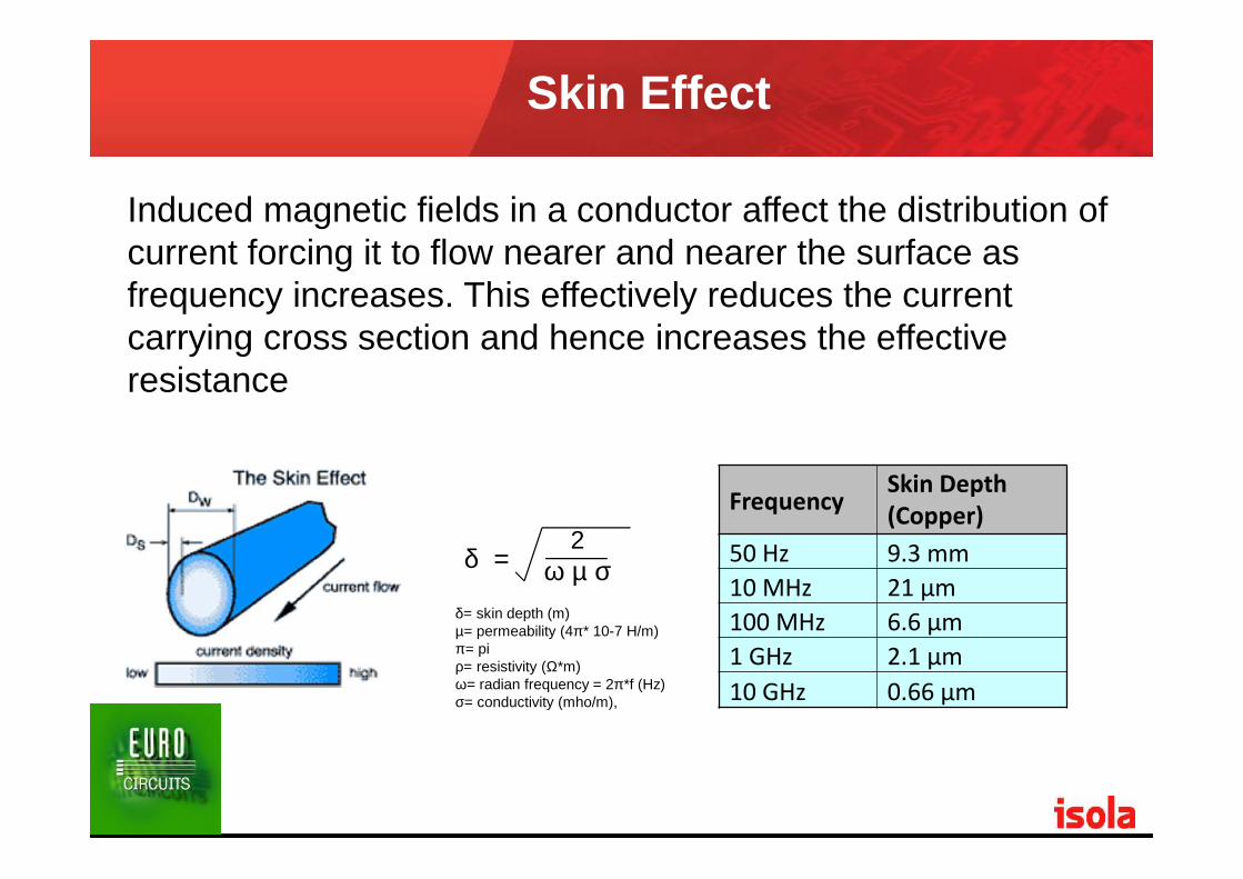
Skin Effect
Induced magnetic fields in a conductor affect the distribution ofcurrent forcing it to flow nearer and nearer the surface asfrequency increases. This effectively reduces the currentcarrying cross section and hence increases the effectiveresistance
δ= skin depth (m)µ= permeability (4π* 10-7 H/m)π= piρ= resistivity (Ω*m)ω= radian frequency = 2π*f (Hz)σ= conductivity (mho/m),
δ =2
ω µ σ
FrequencySkin Depth(Copper)
50 Hz 9.3 mm10 MHz 21 µm100 MHz 6.6 µm1 GHz 2.1 µm10 GHz 0.66 µm

Copper Surface ProfileResist side Bonding side
Frequency Skin Depth10 MHz 21 µm
Signal Path
Frequency Skin Depth100 MHz 6.6 µm
The current is able to tunnelbelow the surface profile andthrough the bulk of the conductor
The current is forced to follow everypeak and trough of the surface profileincreasing path length and resistance
Standard foil
~10 µm

Copper Profile Specifications
LP
eVLP/H-VLP
STD HTE
DSTF/RTF
10 microns
5 - 9.9 microns
< 5 microns
Standard Foil
Low Profile
Very Low Profile

Dielectric Loss
Dielectrics are materials which are poor conductors of electric current.They are insulators because they have few free electrons available tocarry current.
However, when subjected to an electric field polarisation occurswhereby positive and negative charges are displaced relative to theelectric field. This polarisation reduces the electric field in the dielectricthus causing part of the applied field to be lost
+-
Unpolarised+
- +-+
-
+-
+-
+-
+-
+-+-
+-
+-
+-
+-
+-
+-
+-
+-
+-
+ + + + + + + + + + +
- - - - - - - - - - -Polarised by electric field

Dipole Moment
The amount of polarisation that can occur in a dielectric material depends onthe symmetry of the molecular structure and can be quantified by the “DipoleMoment”. Within most molecular structures, although the overall charge is zero,the positive and negative charges do not overlap completely thus giving rise toa permanent Dipole Moment.
A good example of how this works is exhibited by watermolecules in a microwave oven. As the field oscillatesthe molecules continuously rotate releasing kineticenergy as they collide with neighbouring molecules. Themicrowave frequency is 2.45GHz as this frequencyallows the optimal time needed for the molecules torotate exactly 180º.The time delay is crucial to the process and explains whythe dielectric loss reduces at higher frequencies for someadvanced dielectrics where there isn’t enough time forthe molecules to polarise before the charge reverses. O
105°
HH
δ -
δ +
O
105°
H Hδ +
δ -

Loss Factor
The effect of the dipole moment in a dielectric is quantified as “losstangent” and describes the dielectric’s inherent dissipation of anapplied electric field. The loss tangent derives from the tangent of thephase angle between the resistive and reactive components of asystem of complex permittivity. The property is dimensionless and isoften referred to by the following synonyms;
• Loss Factor• Dissipation Factor• Dielectric Loss• Loss angle• Tan δ

Indicative Loss Factor Values
Material Loss factor (1GHz)
Air ~ 0
Alumina 0.0002
Water 0.06
E-glass 0.0012
NE-glass 0.0006
Standard FR4 0.015
Phenolic cured FR4 0.020
Ceramic filled low loss substrate 0.003
PTFE based PCB substrate 0.002
New Generation PCB substrate 0.003
PTFE materials and more recentlyhighly ceramic filled materials havebeen the standard choice fordesigners of high speed circuits
With the market growth andtechnological demands for multilayercircuits, new unfilled, non PTFEsubstrates have been developedenabling greater complexity,improved processability and offeringa lower cost alternative to traditionalsolutions.
I-Tera MT

Eye Diagram
The “Eye”
One Bit Length
Signal withNoise
Good SamplingPeriod
NoiseMargin
Jitter
Noise
Reference: Handbook of Fiber Optics

Simulated Eye Diagrams
I=Tera MT® =.003
Zero Dielectric LossAt Source
IS620 DF =.008FR408 DF =.012
Simulated Eye Diagrams @ 5 Gbps -1 M -50 Ohms impedance5 Mil Track width PRBS 35 PS Rise time
Standard FR4 DF =.020

I-Tera® MT Applications High Speed Digital Long Backplanes -20-30” – 10 Gbps/Channel Daughter cards-10”- 20 Gbps/Channel
RF/Microwave Automotive Radars and Sensors Antennas Low noise block down converters (LNB) for Direct Broadcast Systems Base Stations Power Amplifiers Point to Point Links RFID’s
Competitive products High Speed Digital Megtron-6
RF/MW Rogers 4350 Taconic RF 35

Thermal Coefficient of Dielectric Constant
3.000
3.100
3.200
3.300
3.400
3.500
3.600
3.700
3.800
3.900
4.000
-40 -20 0 23 50 85 105 125
DielectricConstant
Temperature °C
I-Tera TC Dielectric Constant
Dielectric Constant

I-Tera® MT and IS680 vs competitive products
IS680 vs Competition
-0.900
-0.800
-0.700
-0.600
-0.500
-0.400
-0.300
-0.200
-0.100
0.000
1.0 2.0 3.0 4.0 5.0 6.0 7.0 8.0 9.010.0
11.012.0
13.014.0
15.016.0
17.018.0
19.020.0
Frequency in GHz
dB/IN
CH
RO4350B AR 25N IS680-345 IS680-338
20-25 % Improved performance over competitive products
I-Tera™

I-Tera® MT Product Strengths
• I-Tera MT uses Standard E-Glass
• Standard Thicknesses Available (nominal ± 5% for 0.020” and above)
• Full Thin core offering from 0.0020 ( non ZBC ) to 0.018” for multilayer designs
• Square and MS Spread glass weaves used - 1035, 1067, 1086, 1078
• Very low loss material for backplane, high data rate daughter cards, hybrid applications
• Superior Drilling Performance – I-Tera MT does not contain a ceramic filler
• Processing to date - Plasma desmear not required
• I-Tera has passed 10x 370°C re-work simulation testing.
• Compatible with Isola 185HR, 370HR and IS415 for hybrid constructions
• I-Tera MT prepreg can be stored at standard FR4 conditions
• I-Tera MT = UL 94 V- 0
• UL MOT 130 C , I-Tera MT is the UL designation

I-Tera® MT IST TestingIST Test Structure
27
IST Test Structure 16 Layers, 2 mm thick PTH = 300 um drilled dia. Buried Via = 250 µm mm
drilled dia. Microvia = 125 µm drilled
dia. IST Test Pre-Condition 5 x 230 C PTH = RT to 150 C BuriedVia’s = RT to 150 C
L1 Copper Foil
2 x 1067 74%L2
0.1 mm 18/18L3
2 x 1067 74%L4
0.1 mm 18/18L5
2 x 1067 74%L6
0.1 mm 18/18L7
2 x 1067 74%L8
0.1 mm 18/18L9
2 x 1067 74%L10
0.1 mm 18/18L11
2 x 1067 74%L12
0.1 mm 18/18L13
2 x 1067 74%L14
0.1 mm 18/18L15
2 x 1067 74%
L16 Copper Foil

IST Test Results
Initial test results indicated exceptional thermal performance of I-Tera.Six initial IST test coupons were tested : - PTH Holes (indicative of material performance) The IST test was stopped after 2,800 cycles of the PTH
with no failures and no real sign of resistance increasebeing measured. Customer commented that this type of performance was
what would be typically expected of a Polyimide material. In comparison, 370HR (Customer’s “standard” FR4
material) would have been expected to “fail” at 1,000 to1,500 cycles on such a PCB structure.
I-Tera® MT IST Testing

I-Tera® MT – Via Filling
I-Tera Prepreg has shown the ability to fill vias I-Tera 0.020 H/H 3.45 Dk and 1 x 1078 72 % both sides Competitive Product would not fill the via, pre-fill had to be used Isola continues to work on hybrid applications with185HR, IS400, 370HR and IS415
I-Tera0.020” core
I-Tera1078 72 % prepreg
I-Tera1078 72 % prepreg

I-Tera® MT TV with 2 oz planes
10X Lead Free Reflow @260°C shows complete fillof the 2oz copper areasand no de-lamination.

I-Tera® MT TV with 2 oz planes
10X reflow at 260 C
2 oz planes. Crosssections show fill areaof 2 oz copper notingno glass stop oncopper surface and node-lamination

I-Tera® MT
Hybrid PWB
Processing Data

I-Tera® MT Hybrid Processing

Desmear
In Hybrid processing it is recommended to use thecurrent process of the FR-4 component. I-Tera does very
well with both chemical or plasma desmear processeswith a weight loss similar to that seen with FR4 180 Tg
type products.
In the case where a hybrid using a more chemicallyresistant material you will expect to see an increased
etch back on the I-Tera creating a stepped difference inthe two materials.
I-Tera® MT MT Hybrid Processing

Even toward outeredge of boardthere is no sign ofpositive etch back.
Dielectric surfacelooks improved
Glass lookscleaner.
Outer regions ofholes showincreased resinremoval. Positiveetch-back moreapparent.
Glass is veryclean.
Resin shows sometexturing.
Plasma
ChemicalDesmear
800 X
I-Tera® MT plasma vs chemical desmear

I-Tera® MT Dk DataCore Core Standard Resin Dk Dk Dk Dk Dk Dk
Thickness ( in ) Thickness ( mm ) Constructions Content at 100 MHz at 500 MHz at 1 GHz at 2.0 GHz at 5.0 GHz at 10.0 GHz0.002 ( non-ZBC) 0.0500 1 x 1067 63 3.21 3.21 3.21 3.21 3.21 3.21
0.0025 0.0625 1 x 1078 56 3.34 3.34 3.34 3.34 3.34 3.340.0030 0.0750 1 x 1080 62 3.22 3.22 3.22 3.22 3.22 3.220.0030 0.0750 1 x 1078 62 3.22 3.22 3.22 3.22 3.22 3.220.0033 0.0825 1 x 1086 61 3.24 3.24 3.24 3.24 3.24 3.240.0035 0.0875 1 x 1086 63 3.21 3.21 3.21 3.21 3.21 3.210.0040 0.1000 1 x 3313 54 3.38 3.38 3.38 3.38 3.38 3.380.0040 0.1000 2 x 1067 63 3.21 3.21 3.21 3.21 3.21 3.210.0040 0.1000 2 x 1035 64 3.19 3.19 3.19 3.19 3.19 3.190.0045 0.1125 1 x 3313 58 3.30 3.30 3.30 3.30 3.30 3.300.0045 0.1125 2 x 1067 66 3.15 3.15 3.15 3.15 3.15 3.150.0050 0.1250 1 x 2116 53 3.39 3.39 3.39 3.39 3.39 3.390.0050 0.1250 1 x 3313 61 3.24 3.24 3.24 3.24 3.24 3.240.0050 0.1250 2 x 1078 56 3.34 3.34 3.34 3.34 3.34 3.340.0050 0.1250 2 x 1067 69 3.09 3.09 3.09 3.09 3.09 3.090.0055 0.1375 1 x 2116 57 3.32 3.32 3.32 3.32 3.32 3.320.0055 0.1375 2 x 1078 59 3.28 3.28 3.28 3.28 3.28 3.280.0060 0.1500 1 x 2116 60 3.26 3.26 3.26 3.26 3.26 3.260.0060 0.1500 2 x 1080 62 3.22 3.22 3.22 3.22 3.22 3.220.0060 0.1500 2 x 1078 62 3.22 3.22 3.22 3.22 3.22 3.220.0066 0.1650 2 x 1080 65 3.17 3.17 3.17 3.17 3.17 3.170.0066 0.1650 2 x 1078 65 3.17 3.17 3.17 3.17 3.17 3.170.0070 0.1750 2 x 1086 63 3.21 3.21 3.21 3.21 3.21 3.210.0080 0.2000 2 x 3313 54 3.38 3.38 3.38 3.38 3.38 3.380.0090 0.2250 2 - 3313 58 3.30 3.30 3.30 3.30 3.30 3.300.0100 0.2500 3313/ 1652 50 3.45 3.45 3.45 3.45 3.45 3.450.0100 0.2500 2 x 2116 53 3.39 3.39 3.39 3.39 3.39 3.390.0100 0.2500 2 x 3313 61 3.24 3.24 3.24 3.24 3.24 3.240.0120 0.3000 2 - 3313 / 1067 61 3.24 3.24 3.24 3.24 3.24 3.240.0130 0.3250 2 - 3313 / 1080 61 3.24 3.24 3.24 3.24 3.24 3.240.0133 0.3325 2 - 3313/ 1086 61 3.24 3.24 3.24 3.24 3.24 3.240.0140 0.3500 3 - 3313 59 3.28 3.28 3.28 3.28 3.28 3.280.0150 0.3750 3 - 3313 61 3.24 3.24 3.24 3.24 3.24 3.240.0150 0.3750 3 - 2116 53 3.39 3.39 3.39 3.39 3.39 3.390.0160 0.4000 2 - 3313 / 2116 58 3.30 3.30 3.30 3.30 3.30 3.300.0160 0.4000 2 - 3313 / 2 - 1078 61 3.24 3.24 3.24 3.24 3.24 3.240.0166 0.4150 2- 3313 / 2 - 1078 62 3.22 3.22 3.22 3.22 3.22 3.220.0180 0.4500 2- 3313 / 2 - 3313 58 3.30 3.30 3.30 3.30 3.30 3.300.0200 0.5000 2 - 3313/ 2 - 1652 50 3.45 3.45 3.45 3.45 3.45 3.450.0200 0.5000 4 - 2116 54 3.38 3.38 3.38 3.38 3.38 3.380.0300 0.7500 5 - 1652 50 3.45 3.45 3.45 3.45 3.45 3.450.0300 0.7500 6 - 2116 54 3.38 3.38 3.38 3.38 3.38 3.38

I-Tera® MT Df DataCore Core Standard Resin Df Df Df Df Df Df
Thickness Thickness ( mm ) Constructions Content at 100 MHz at 500 MHz at 1 GHz at 2.0 GHz at 5.0 GHz at 10.0 GHz0.002 ( non-ZBC ) 0.0500 1 x 1067 63 0.0032 0.0033 0.0034 0.0034 0.0034 0.0034
0.0025 0.0625 1 x 1078 56 0.0034 0.0035 0.0036 0.0036 0.0036 0.00360.0030 0.0750 1 x 1080 62 0.0032 0.0033 0.0034 0.0034 0.0034 0.00340.0030 0.0750 1 x 1078 62 0.0032 0.0033 0.0034 0.0034 0.0034 0.00340.0033 0.0825 1 x 1086 61 0.0033 0.0034 0.0035 0.0035 0.0035 0.00350.0035 0.0875 1 x 1086 63 0.0032 0.0033 0.0034 0.0034 0.0034 0.00340.0040 0.1000 1 x 3313 54 0.0035 0.0036 0.0037 0.0037 0.0037 0.00370.0040 0.1000 2 x 1067 63 0.0032 0.0033 0.0034 0.0034 0.0034 0.00340.0040 0.1000 2 x 1035 64 0.0032 0.0033 0.0034 0.0034 0.0034 0.00340.0045 0.1125 1 x 3313 58 0.0034 0.0035 0.0036 0.0036 0.0036 0.00360.0045 0.1125 2 x 1067 66 0.0031 0.0032 0.0033 0.0033 0.0033 0.00330.0050 0.1250 1 x 2116 53 0.0035 0.0036 0.0037 0.0037 0.0037 0.00370.0050 0.1250 1 x 3313 61 0.0033 0.0034 0.0035 0.0035 0.0035 0.00350.0050 0.1250 2 x 1078 56 0.0034 0.0035 0.0036 0.0036 0.0036 0.00360.0050 0.1250 2 x 1067 69 0.0030 0.0031 0.0032 0.0032 0.0032 0.00320.0055 0.1375 1 x 2116 57 0.0034 0.0035 0.0036 0.0036 0.0036 0.00360.0055 0.1375 2 x 1078 59 0.0033 0.0034 0.0035 0.0035 0.0035 0.00350.0060 0.1500 1 x 2116 60 0.0033 0.0034 0.0035 0.0035 0.0035 0.00350.0060 0.1500 2 x 1080 62 0.0032 0.0033 0.0034 0.0034 0.0034 0.00340.0060 0.1500 2 x 1078 62 0.0032 0.0033 0.0034 0.0034 0.0034 0.00340.0066 0.1650 2 x 1080 65 0.0031 0.0032 0.0033 0.0033 0.0033 0.00330.0066 0.1650 2 x 1078 65 0.0031 0.0032 0.0033 0.0033 0.0033 0.00330.0070 0.1750 2 x 1086 63 0.0032 0.0033 0.0034 0.0034 0.0034 0.00340.0080 0.2000 2 x 3313 54 0.0035 0.0036 0.0037 0.0037 0.0037 0.00370.0090 0.2250 2 - 3313 58 0.0034 0.0035 0.0036 0.0036 0.0036 0.00360.0100 0.2500 3313/ 1652 50 0.0038 0.0038 0.0038 0.0038 0.0038 000380.0100 0.2500 2 x 2116 53 0.0035 0.0036 0.0037 0.0037 0.0037 0.00370.0100 0.2500 2 x 3313 61 0.0033 0.0034 0.0035 0.0035 0.0035 0.00350.0120 0.3000 2 - 3313 / 1067 61 0.0033 0.0034 0.0035 0.0035 0.0035 0.00350.0130 0.3250 2 - 3313 / 1080 61 0.0033 0.0034 0.0035 0.0035 0.0035 0.00350.0133 0.3325 2 - 3313/ 1086 61 0.0033 0.0034 0.0035 0.0035 0.0035 0.00350.0140 0.3500 3 - 3313 59 0.0033 0.0034 0.0035 0.0035 0.0035 0.00350.0150 0.3750 3 - 3313 61 0.0033 0.0034 0.0035 0.0035 0.0035 0.00350.0150 0.3750 3 - 2116 53 0.0035 0.0036 0.0037 0.0037 0.0037 0.00370.0160 0.4000 2 - 3313 / 2116 58 0.0034 0.0035 0.0036 0.0036 0.0036 0.00360.0160 0.4000 2 - 3313 / 2 - 1078 61 0.0033 0.0034 0.0035 0.0035 0.0035 0.00350.0166 0.4150 2- 3313 / 2 - 1078 62 0.0032 0.0033 0.0034 0.0034 0.0034 0.00340.0180 0.4500 2- 3313 / 2 - 3313 58 0.0034 0.0035 0.0036 0.0036 0.0036 0.00360.0200 0.5000 2 - 3313/ 2 - 1652 50 0.0038 0.0038 0.0038 0.0038 0.0038 000380.0200 0.5000 4 - 2116 54 0.0035 0.0036 0.0037 0.0037 0.0037 0.00370.0300 0.7500 5 - 1652 50 0.0038 0.0038 0.0038 0.0038 0.0038 000380.0300 0.7500 6 - 2116 54 0.0035 0.0036 0.0037 0.0037 0.0037 0.0037
.

Prepreg Resin Thickness Thickness Dk Dk Dk Dk Dk DkContent ( in ) ( mm ) at 100 MHz at 500 MHz at 1 GHz at 2.0 GHz at 5.0 GHz at 10.0 GHz
1035 61 0.0018 0.0450 3.24 3.24 3.24 3.24 3.24 3.241035 64 0.0020 0.0500 3.19 3.19 3.19 3.19 3.19 3.191067 66 0.0023 0.0575 3.15 3.15 3.15 3.15 3.15 3.151067 69 0.0025 0.0625 3.09 3.09 3.09 3.09 3.09 3.091067 74 0.0031 0.0775 3.00 3.00 3.00 3.00 3.00 3.001078 66 0.0035 0.0875 3.15 3.15 3.15 3.15 3.15 3.151078 70 0.0040 0.1000 3.07 3.07 3.07 3.07 3.07 3.071078 72 0.0044 0.1100 3.04 3.04 3.04 3.04 3.04 3.041086 63 0.0035 0.0875 3.21 3.21 3.21 3.21 3.21 3.211086 66 0.0039 0.0975 3.15 3.15 3.15 3.15 3.15 3.151086 69 0.0044 0.1100 3.09 3.09 3.09 3.09 3.09 3.091080 67 0.0035 0.0875 3.13 3.13 3.13 3.13 3.13 3.131080 71 0.0040 0.1000 3.05 3.05 3.05 3.05 3.05 3.053313 54 0.0040 0.1000 3.38 3.38 3.38 3.38 3.38 3.383313 58 0.0045 0.1125 3.30 3.30 3.30 3.30 3.30 3.303313 61 0.0050 0.1250 3.24 3.24 3.24 3.24 3.24 3.242116 57 0.0055 0.1375 3.32 3.32 3.32 3.32 3.32 3.322116 60 0.0060 0.1500 3.26 3.26 3.26 3.26 3.26 3.26
Prepreg Resin Thickness Thickness Df Df Df Df Df DfContent ( in ) ( mm ) at 100 MHz at 500 MHz at 1 GHz at 2.0 GHz at 5.0 GHz at 10.0 GHz
1035 61 0.0018 0.0450 0.0033 0.0034 0.0035 0.0035 0.0035 0.00351035 64 0.0020 0.0500 0.0032 0.0033 0.0034 0.0034 0.0034 0.00341067 66 0.0023 0.0575 0.0031 0.0032 0.0033 0.0033 0.0033 0.00331067 69 0.0025 0.0625 0.0030 0.0031 0.0032 0.0032 0.0032 0.00321067 74 0.0031 0.0775 0.0029 0.0029 0.0030 0.0030 0.0030 0.00301078 66 0.0035 0.0875 0.0031 0.0032 0.0033 0.0033 0.0033 0.00331078 70 0.0040 0.1000 0.0031 0.0031 0.0032 0.0032 0.0032 0.00321078 72 0.0044 0.1100 0.0030 0.0030 0.0031 0.0031 0.0031 0.00311086 63 0.0035 0.0875 0.0032 0.0033 0.0034 0.0034 0.0034 0.00341086 66 0.0039 0.0975 0.0031 0.0032 0.0033 0.0033 0.0033 0.00331086 69 0.0044 0.1100 0.0030 0.0031 0.0032 0.0032 0.0032 0.00321080 67 0.0035 0.0875 0.0031 0.0032 0.0033 0.0033 0.0033 0.00331080 71 0.0040 0.1000 0.0030 0.0030 0.0031 0.0031 0.0031 0.00313313 54 0.0040 0.1000 0.0035 0.0036 0.0037 0.0037 0.0037 0.00373313 58 0.0045 0.1125 0.0034 0.0035 0.0036 0.0036 0.0036 0.00363313 61 0.0050 0.1250 0.0033 0.0034 0.0035 0.0035 0.0035 0.00352116 57 0.0055 0.1375 0.0034 0.0035 0.0036 0.0036 0.0036 0.00362116 60 0.0060 0.1500 0.0033 0.0034 0.0035 0.0035 0.0035 0.0035
I-Tera® MT Dk Df - Prepreg

Tin / Lead AssemblyCompatible
Lead Free Assembly Compatible
370HR 180 TgLow CTE High Reliability
FR408 180TgLow Dk & Df
IS415 200 TgMid Dk/Df
IS620i Tg 225 Low LossDf 0.0070 @10 GHz
I-Tera® MT -High Tg Very Low LossDf - 0.0035 @ 10 GHz
I-Speed® - 180 TgDf 0.0065 @ 10 GHz
FR408HR 200 TgLow Df, Low CTE
DE156 155 TgHalogen Free
FR406 High Tg170° Epoxy
G200BT / Epoxy
GETEK® 180TgMid Dk & Df
185HR > 170 TgLead Free Assbly Std Dk Df
FR408HRIS 200 TgFR408HR Low Dk Glass
New Products
Auto-HR 170 Tg0.014, 0.028, 0.035 & 0.042
Thick cores
GreenSpeed™ 175 TgHalogen Free
I-Speed®IS - 180 TgI-Speed on Low Dk glass
Speed is a function of design such as line length etc.** Laminate Data - IST performance is a function of Hole diameter, board thickness, plating parameters and laminate attributes.
T260 – 10 min.
Td – 300C**
T288 - 60 Min.
Td – 400C**
1 GHz 20 GHz
Impr
ovin
g Th
erm
al P
erfo
rman
ce–
T 26
0 / T
d / I
ST
Improving Electrical Performance – Lower Dk/Df – Higher Speed
More reliable
Higher Speeds
Product positioning map
DSTF, DSRFoil, DSRFoil, GETEK, I-Fill, I-Speed, I-Tera, IsoDesign, Isola, IsoStack, Norplex, Polyclad, RCC, Lo-Flo and TURBO are registeredtrademarks of Isola USA Corp. in the U.S.A. and other countries. The Isola logo is a trademark of Isola USA Corp. in the U.S.A. and other countries.All other trademarks mentioned herein are property of their respective companies. Copyright © 2013 Isola Group, S.à.r.l. All rights reserved.


