From Specification to Silicon: Towards Analog/Mixed-Signal Design Automation using Surrogate NN Models with Transfer Learning Juzheng Liu 1 , Shiyu Su 1 , Meghna Madhusudan 2 , Mohsen Hassanpourghadi 1 , Samuel Saunders 1 , Qiaochu Zhang 1 , Rezwan Rasul 1 , Yaguang Li 3 , Jiang Hu 3 , Arvind Kumar Sharma 3 , Sachin S. Sapatnekar 2 , Ramesh Harjani 2 , Anthony Levi 1 , Sandeep Gupta 1 and Mike Shuo-Wei Chen 1 1 Department of Electrical and Computer Engineering, University of Southern California 2 Department of Electrical and Computer Engineering, University of Minnesota 3 Department of Electrical and Computer Engineering,Texas A&M University Los Angeles, CA, USA Email: [email protected]Abstract—We propose a complete analog mixed-signal circuit design flow from specification to silicon with minimum human- in-the-loop interaction, and verify the flow in a 12nm FinFET CMOS process. The flow consists of three key elements: neural network (NN) modeling of the parameterized circuit component, a search algorithm based on NN models to determine its sizing, and layout automation. To reduce the required training data for NN model creation, we utilize transfer learning to improve the NN accuracy from a relatively small amount of post- layout/silicon data. To prove the concept, we use a voltage- controlled oscillator (VCO) as a test vehicle and demonstrate that our design methodology can accurately model the circuit and generate designs with a wide range of specifications. We show that circuit sizing based on the transfer learned NN model from silicon measurement data yields the most accurate results. Index Terms—AMS circuit design automation, circuit model- ing, layout automation, silicon verified CAD I. I NTRODUCTION With the development of advanced technology, analog mixed-signal (AMS) circuit design is becoming more of a challenge due to increased relative design cost. As an example, FinFET CMOS technologies involve much longer simulation time in both schematic and post-layout level, and impose more complex layout rules compared to bulk CMOS technology. This severely limits design exploration for an optimal design such as architecture, device sizing, and biasing, given a target AMS specification and limited design time. Therefore, AMS circuit design automation can play a crucial role in resolving these challenges. There have been several prior efforts aimed at implementing AMS design automation. At the circuit architecture level, one approach has been to adopt a mostly digital AMS architecture using digital standard cells, allowing conventional digital design automation flow to lower the design cost [1], [2]. However, this digital-library- based AMS circuit design still requires the involvement of human designers in schematic designs and layout iterations. For schematic design exploration, Bayesian Optimization (BO) [3] and Artificial Neural Networks (ANN) [4], [5] have been applied to automatically size the netlist and significantly reduce the effort required from human designers in the early design stages. However, this prior art mainly focused on schematic-level design without layout. [6] further explored general circuit sizing for both schematic and layout with Reinforcement Learning (RL). However, this can be very time consuming for layout design since it requires a large number of real-time post-layout simulation steps. In this work, we propose a complete AMS circuit design automation flow from target design specification to layout with significantly reduced human intervention and design time. To achieve design automation and facilitate design- space exploration, we integrate an NN model-based circuit sizing algorithm [4] with the ALIGN [7] layout automation flow. To enhance the accuracy of the NN model for design exploration while minimizing the training cost, we apply Transfer Learning (TL) [8] to the NN model in later design stages, including post-layout and silicon measurement. In a nutshell, the NN-based circuit surrogate model is created using relatively low-cost schematic simulations. Next, TL takes a few post-layout simulation samples from the ALIGN layout flow, and effectively transfers the schematic-level model to the post-layout model, which can be used for layout-aware circuit sizing. Lastly, to overcome the modeling and layout extraction inaccuracy, especially for high frequency AMS circuit designs, we further enhance the NN model by TL with the silicon measurement data, i.e., a silicon-level NN model. To prove the effectiveness of our design flow, we taped out various VCO test structures and demonstrated that the circuit sizing based on the silicon-level NN model yields the most accurate sizing result. From the standpoint of real applications, the proposed design flow can be useful in many ways. If the user needs to precisely design for a certain target circuit specification, the flow can efficiently model and size the circuit with the layout parasitic extraction (LPE) information included, which can be much faster than manual layout iterations or layout-
Transcript
From Specification to Silicon: TowardsAnalog/Mixed-Signal Design Automation usingSurrogate NN Models with Transfer LearningJuzheng Liu1, Shiyu Su1, Meghna Madhusudan2, Mohsen Hassanpourghadi1, Samuel Saunders1,
Qiaochu Zhang1, Rezwan Rasul1, Yaguang Li3, Jiang Hu3, Arvind Kumar Sharma3,Sachin S. Sapatnekar2, Ramesh Harjani2, Anthony Levi1, Sandeep Gupta1 and Mike Shuo-Wei Chen1
1Department of Electrical and Computer Engineering, University of Southern California2Department of Electrical and Computer Engineering, University of Minnesota3Department of Electrical and Computer Engineering,Texas A&M University
Abstract—We propose a complete analog mixed-signal circuitdesign flow from specification to silicon with minimum human-in-the-loop interaction, and verify the flow in a 12nm FinFETCMOS process. The flow consists of three key elements: neuralnetwork (NN) modeling of the parameterized circuit component,a search algorithm based on NN models to determine its sizing,and layout automation. To reduce the required training datafor NN model creation, we utilize transfer learning to improvethe NN accuracy from a relatively small amount of post-layout/silicon data. To prove the concept, we use a voltage-controlled oscillator (VCO) as a test vehicle and demonstratethat our design methodology can accurately model the circuitand generate designs with a wide range of specifications. Weshow that circuit sizing based on the transfer learned NN modelfrom silicon measurement data yields the most accurate results.
With the development of advanced technology, analogmixed-signal (AMS) circuit design is becoming more ofa challenge due to increased relative design cost. As anexample, FinFET CMOS technologies involve much longersimulation time in both schematic and post-layout level, andimpose more complex layout rules compared to bulk CMOStechnology. This severely limits design exploration for anoptimal design such as architecture, device sizing, and biasing,given a target AMS specification and limited design time.Therefore, AMS circuit design automation can play a crucialrole in resolving these challenges. There have been severalprior efforts aimed at implementing AMS design automation.At the circuit architecture level, one approach has been toadopt a mostly digital AMS architecture using digital standardcells, allowing conventional digital design automation flow tolower the design cost [1], [2]. However, this digital-library-based AMS circuit design still requires the involvement ofhuman designers in schematic designs and layout iterations.For schematic design exploration, Bayesian Optimization (BO)[3] and Artificial Neural Networks (ANN) [4], [5] have been
applied to automatically size the netlist and significantlyreduce the effort required from human designers in the earlydesign stages. However, this prior art mainly focused onschematic-level design without layout. [6] further exploredgeneral circuit sizing for both schematic and layout withReinforcement Learning (RL). However, this can be very timeconsuming for layout design since it requires a large numberof real-time post-layout simulation steps.
In this work, we propose a complete AMS circuit designautomation flow from target design specification to layoutwith significantly reduced human intervention and designtime. To achieve design automation and facilitate design-space exploration, we integrate an NN model-based circuitsizing algorithm [4] with the ALIGN [7] layout automationflow. To enhance the accuracy of the NN model for designexploration while minimizing the training cost, we applyTransfer Learning (TL) [8] to the NN model in later designstages, including post-layout and silicon measurement. In anutshell, the NN-based circuit surrogate model is created usingrelatively low-cost schematic simulations. Next, TL takes afew post-layout simulation samples from the ALIGN layoutflow, and effectively transfers the schematic-level model to thepost-layout model, which can be used for layout-aware circuitsizing. Lastly, to overcome the modeling and layout extractioninaccuracy, especially for high frequency AMS circuit designs,we further enhance the NN model by TL with the siliconmeasurement data, i.e., a silicon-level NN model. To prove theeffectiveness of our design flow, we taped out various VCOtest structures and demonstrated that the circuit sizing basedon the silicon-level NN model yields the most accurate sizingresult.
From the standpoint of real applications, the proposeddesign flow can be useful in many ways. If the user needsto precisely design for a certain target circuit specification,the flow can efficiently model and size the circuit with thelayout parasitic extraction (LPE) information included, whichcan be much faster than manual layout iterations or layout-
level parameter sweeps. When multiple different design targetsneed to be fulfilled, the advantage of this design flow canbe greater. Unlike BO- or RL-based circuit sizing, the NNmodel based searching algorithm can quickly size the circuitto meet different specifications without the need for extramodeling or simulation, and the layout tool can automaticallygenerate the corresponding layouts without human interaction.Furthermore, when silicon test structures are available (whichis usually the case for real product development), the modelcan be further enhanced by TL and the sizing results can beeven closer to the expected values as shown by comprehensiveexperiments.
The remaining part of the paper is arranged as follows:Section II will discuss the existing circuit design automationapproaches. Section III will introduce the proposed design flowin detail. Section IV contains the experimental results usingthe proposed flow, and the last section will conclude the wholework.
II. RELATED WORK
In this section, we will discuss several directions for circuitdesign automation flow and compare the advantages anddisadvantages in terms of flow completeness, design timeconsumption, and required human intervention.
A. Digital library based fully synthesized AMS circuit
The first widely used automatic AMS circuit generationmethod is to use a digital standard cell library and realize theAMS circuit function via digital gates. For instance, in [2],the authors used a set of parallel NAND gates as a varactorand binary scaled inverters as a digital-to-analog converter torealize a fully synthesized digital controlled oscillator using adigital synthesis and layout tool. In [1], the authors customizedthe standard cell library to include some analog blocks, andused RTL to synthesize an analog-to-digital converter. Theadvantage of this method is that it leverages commerciallyavailable digital design flow and hence accelerates the designprocess. However, the mostly digital architecture cannot begeneralized to cover the entire range of AMS specifications.Moreover, significant human design effort is still needed,involving intensive layout iterations. Lastly, such a designapproach faces a lack of automatic netlist sizing tools thatcan meet target analog design specifications.
B. Reinforcement learning-based circuit design automation
Different from the first approach, [6] leverages RL to designthe circuit for a target along a trajectory to automatically sizethe components in the netlist and generate the schematic. Froma certain starting design point, the RL agent will make adecision on how to change each design parameter, and thesimulation result for this step will be collected for the nextdecision. The RL agent is trained by the policy gradient,and requires a large number of environmental steps. Aftertraining, for most of the design targets in the predefined targetspace, the agent can successfully find the right design withina few steps. From one perspective, this design approach is
able to generate different designs efficiently without humanintervention. Nevertheless, when considering the post-layoutdesign stage, the design agent requires real-time post-layoutsimulations steps which can consume a significant amount ofcomputation time. Furthermore, when several designs withvarious specifications are needed, the RL agent needs togenerate the trajectory with post-layout simulation steps foreach of the designs, which can be even more time-consuming.
C. Bayesian optimization-based circuit design automation
Another circuit sizing method uses BO to directly tune thecircuit under design. After determining the design parametersand metrics, a reward is constructed as a function of themetrics according to the design target. A few samples arerandomly selected from the design space to initialize theGaussian Process Regression (GPR) model between the designparameters and reward functions. Then an acquisition functionis constructed according to the probabilistic prediction of theGPR model in the whole design space, and the next samplethat maximizes the acquisition function will be selected andused to update the GPR model. [3] shows that by deliberatelydesigning the reward and acquisition function, BO can effec-tively optimize the circuit towards the target. Unfortunately,layout-level design examples were not demonstrated in [3]. Incircumstances where a layout automation tool is incorporatedwith the BO-based circuit sizing algorithm, this approach canbe time consuming, since the optimization process may involvehundreds or even thousands of post-layout simulations.
D. Model-based circuit design automation
This class of methods avoids the time-consuming real-timesimulation requirement, mentioned in Sections II-B and II-C,by first training a circuit surrogate model and then directlyapplying search algorithms based on the surrogate model. In[5], the authors train an NN as the surrogate model of thecircuit under design and apply a local minimum search tofind optimal circuit sizing. [4] further improves the model-based search algorithm by breaking large-scale AMS circuitsinto a set of smaller-scale modules, each represented by asurrogate NN model. It then constructs a complete surrogateNN model by connecting all the modules with a module-linking graph to facilitate netlist sizing via a gradient-basedsearch algorithm. While the search over the surrogate model isfast, the disadvantage of the NN model-based approach is theneed for a training dataset, and that it can involve expensivesimulation time especially when post-layout simulations areconsidered.
To alleviate the aforementioned limitations, we propose anAMS circuit design automation flow that combines the model-based search algorithm and the ALIGN layout automationtool to complete a design flow from design specification tosilicon. We further apply the TL technique to the model-based searching flow to generate the post-layout/silicon-levelmodel and perform the circuit sizing with better efficiency andaccuracy.
1. NN-based surrogate model
training
Circuit topology definition
2. Layout automation & Post-layout
simulation
3. Transfer learning-based post-layout circuit modeling
Design Target
4. Automatic circuit sizing/layout
Final GDS/tapeout
5. Transfer learning-based silicon-level
circuit modeling
silicon testing data
Fig. 1: Proposed design flow from specification to silicon
III. DESIGN AUTOMATION FLOW
In this work, we propose a complete design automationflow, as shown in Fig. 1, which can efficiently and accuratelysize and layout a circuit netlist for a given specification.Given a certain AMS circuit topology, we will first createa circuit surrogate model in steps 1 to 3 with the layoutinformation considered, and then size and layout the circuit instep 4 without the need for further simulations. In step 1, westart with modeling the circuit Parameters-to-Metrics (P2M)function by sampling with low-cost schematic simulations andtraining of an NN as the circuit surrogate model from scratch.To incorporate the LPE information into the surrogate model,step 2 uses the ALIGN layout automation tool and createsseveral layouts that are randomly selected in the design space.In step 3, with the layouts from step 2 extracted and simulated,TL is applied to efficiently transfer the schematic-level circuitmodel to the post-layout model. Once the surrogate modelis prepared, in step 4, a fast gradient-based search algorithmis applied to find the optimal design parameters given one ormultiple design specifications, and the same layout automationtool is applied to generate the final GDSII. Furthermore,if the design proceeds to fabrication, in step 5, the siliconmeasurement results can be utilized by TL to further improvethe circuit modeling accuracy, and a more precise circuitsizing can be derived. The details of each design step willbe discussed as follows.
A. NN-based surrogate model training
The first step of the proposed design flow is to characterizethe behavior of the AMS circuit under design. We build aparameterized netlist and model the parameters (p) to metrics(m) function:
m = f(p), (1)
where p is defined as a vector of tunable circuit parameterssuch as transistor sizes, and m is defined as the vector ofperformance metrics of the circuit block such as power con-sumption. To model the function f by an NN, we generate thetraining dataset through SPICE simulations. More specifically,in the design space where each dimension is a parameter,we define the upper and lower bond of each parameter andrandomly sample for design points. SPICE simulation is thenperformed for each point, and the corresponding metrics areused as the golden reference in the training.
When training an NN surrogate model, we try to minimizethe Mean Squared Error (MSE) between the model predicted
metrics and the simulation results. Since the numerical value ofdifferent parameters/metrics can be different in orders of mag-nitude, each parameter/metric is linearly re-scaled to [−1, 1]according to the corresponding minimum and maximum valueof the whole dataset. When performing the training, we usethe Adam [9] optimizer to minimize the MSE defined as:
MSE =1
k
k∑i=1
(m̂i −mi)2, (2)
where m̂i is the predicted ith metric from the model, mi isthe ground truth of the ith metric from the simulation, and kis the number of metrics for this circuit block.
B. Automatic layout generation
Layout parasitics and layout-dependent effects are signifi-cant in advanced technology nodes [10], [11] and they affectcircuit performance to a large extent. Both steps 2 and 4 of theflow use a fast automatic layout generator and extract layoutparasitics to analyze the post-layout performance of a design.The open-source ALIGN [7], [12] software is used for layoutgeneration.
ALIGN (“Analog Layout, Intelligently Generated fromNetlists”) takes a SPICE netlist of a circuit as input andgenerates its layout as a GDSII file. For the proposed flow,parameterized netlists of a circuit are fed into ALIGN, andtheir corresponding layouts are extracted and simulated. Sev-eral optimization steps are added to ALIGN to ensure a high-performing layout is generated for each input circuit netlist.
Fig. 2: Overview of the ALIGN layout generation process [12]
ALIGN has a modular approach as shown in Fig. 2. Themain modules in ALIGN that were used in this work in-clude netlist annotation where common building blocks called“primitives” and symmetries in the circuit are detected. Designrule capture is used to abstract the proprietary PDK into asimplified grid which the other modules obey. Parameterized
primitive cell generation automatically builds layouts for theprimitives using the number of fins and fingers in a tran-sistor as parameters. Hierarchical block assembly performsplacement and routing while meeting geometric and electricalconstraints provided to it.
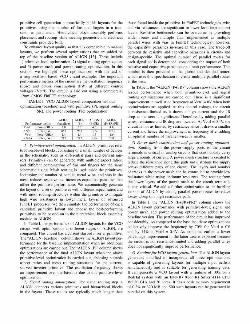
To enhance layout quality so that it is comparable to manuallayouts, we perform several optimizations that are added ontop of the baseline version of ALIGN [13]. These include1) primitive-level optimization, 2) signal routing optimization,and 3) power mesh and power routing optimization. In thissection, we highlight these optimizations with the aid ofa ring-oscillator-based VCO circuit example. The importantperformance metrics of the circuit are the oscillation frequency(Fosc) and power consumption (PW) at different controlvoltages (Vctrl). The circuit is laid out using a commercial12nm CMOS FinFET technology.
TABLE I: VCO ALIGN layout comparison withoutoptimization (baseline) and with primitive (P), signal routing
1) Primitive-level optimization: In ALIGN, primitives referto lowest-level blocks, consisting of a small number of devicesin the schematic, such as differential pairs and current mir-rors. Primitives can be generated with multiple aspect ratios,and different combinations of fins and fingers for the sameschematic sizing. Mesh routing is used inside the primitives.Increasing the number of parallel metal wires and vias in themesh reduces resistive and increases capacitive parasitics thataffect the primitive performance. We automatically generatethe layout of a set of primitives with different aspect ratios andwith mesh routing structures within the primitive to mitigatehigh wire resistances in lower metal layers of advancedFinFET processes. We then simulate the performance of eachcandidate primitive layout and choose the best-performingprimitives to be passed on to the hierarchical block assemblymodule in ALIGN.
In Table I, the performance of ALIGN layouts for the VCOcircuit, with optimizations at different stages of ALIGN, arecompared. This circuit has a current starved inverter primitive.The “ALIGN (baseline)” column shows the ALIGN layout per-formance for the baseline implementation when no additionaloptimizations are carried out. The “ALIGN (P)” column showsthe performance of the final ALIGN layout when the aboveprimitive-level optimization is carried out, choosing suitableaspect ratios and mesh routing structures for the current-starved inverter primitive. The oscillation frequency showsan improvement over the baseline due to this primitive-leveloptimization.
2) Signal routing optimization: The signal routing step inALIGN connects various primitives and hierarchical blocksin the layout. These routes are typically much longer than
those found inside the primitive. In FinFET technologies, wireand via resistances are significant in lower-level interconnectlayers. Resistive bottlenecks can be overcome by providingwider routes and multiple vias (implemented as multipleparallel wires with vias in FinFET technologies); however,the capacitive parasitics increase in this case. The trade-offbetween the resistive and capacitive parasitics is circuit- anddesign-specific. The optimal number of parallel routes foreach signal net is determined, considering the impact of bothresistive and capacitive parasitics on circuit performance. Thisnumber is then provided to the global and detailed router,which uses this specification to create multiple parallel routesat the nets.
In Table I, the “ALIGN (P+SR)” column shows the ALIGNlayout performance when both primitive-level and signalrouting optimizations are carried out. There is a significantimprovement in oscillation frequency at Vctrl = 0V when bothoptimizations are applied. At this control voltage, the circuitis resistance-limited as it draws a high current and the IRdrop at the nets is significant. Therefore, by adding parallelwires, resistance and IR drop are lowered. At Vctrl = 0.4V, thecircuit is not as limited by resistance since it draws a smallercurrent and hence the improvement in frequency after addingan optimal number of parallel wires is smaller.
3) Power mesh construction and power routing optimiza-tion: Routing from the power supply ports to the circuitterminals is critical in analog circuits that continuously carrylarge amounts of current. A power mesh structure is created toreduce the resistance along this path and distribute the supplyacross different parts of the circuit. The layers and numberof tracks in the power mesh can be controlled to provide lowresistance while using optimum resources. The routing fromthe lower layers of the power mesh to the circuit terminalsis also critical. We add a further optimization to the baselineversion of ALIGN by adding parallel power routes to reducelosses along this high resistance path.
In Table I, the “ALIGN (P+SR+PR)” column shows theALIGN layout performance with primitive-level, signal andpower mesh and power routing optimization added to thebaseline version. The performance of the circuit has improvedconsiderably. As compared to the baseline, these optimizationscollectively improve the frequency by 70% for Vctrl = 0Vand by 14% at Vctrl = 0.4V. As explained earlier, a lowerpercentage improvement in the latter case is expected becausethe circuit is not resistance-limited and adding parallel wiresdoes not significantly improve performance.
4) Runtime for VCO layout generation: The ALIGN layoutgenerator, modified to incorporate all three optimizations,is capable of generating layouts for multiple input netlistssimultaneously and is suitable for generating training data.It can generate a VCO layout with a runtime of 100s on aRedHat system with an Intel(R) Xeon(R) Silver 4114 [email protected] GHz and 20 cores. It has a peak memory requirementof 0.2% or 320 MB and 500 such layouts can be generated inparallel on this system.
C. TL-based model enhancement for accurate P2M modeling
For step 3 of the proposed design flow, we need to in-corporate the LPE information into the surrogate model toensure that the model can predict the real-world silicon resultmore accurately. However, it is difficult to train a modelfrom scratch using only the post-layout dataset because post-layout simulations can take a long time. For instance, in12nm FinFET technology, post-layout simulations typicallyconsumes 20 to 30 times longer than the schematic-levelsimulations for the same circuit. To make post-layout modelingfeasible, we utilize the TL technique from [8] to reuse theschematic-level model. More specifically, we add two linearlayers to the input and output of a well-trained schematic-levelsurrogate model. When performing the training, only the twonewly added layers are updated, and the remaining layers arefixed. Mathematically, the post-layout model is constructed asfollows:
f̂layout(p) = Af̂sch(Cp+ d) + b = m̂lay, (3)
where f̂sch is the schematic-level surrogate model, and f̂layoutis the post-layout-level surrogate model. With n parametersand k metrics, C (an n × n matrix) and d (a 1 × n biasvector) are the mapping function of the parameters, i.e., theadded input linear layer, while A (a k × k matrix) and b (a1× k bias vector) are the mapping function of the metrics, orthe added output linear layer. To justify the use of linear TLlayers between schematic and post-layout model, we performpropagation delay analysis of an inverter for illustration pur-pose. If we express the inverter delay as a function of the widthand length of the PMOS and NMOS, assuming NMOS andPMOS have the same size, the schematic-level delay withoutlayout parasitics can be approximated as follows:
td,sch(p) = 0.69CLRon;p = (W,L), (4)
CL = CoxWL+ 2CovW + 2Cdb, (5)
Ron =3VDD
4k′[(VDD − VT )Vdsat −V 2dsat
2 ]WL
(1− 7
9λVDD
)(6)
If we regard the terms that are irrelavent to W and L in (6) asconstants and lump them into α, the equation can be simplifiedas follows:
td,sch = α(CoxWL+ 2CovW + 2Cdb)L
W(7)
After the inverter is laid out, there will be a parasitic resistancein series with Ron, and a parasitic capacitance in parallel withCL, which can be reasonably estimated as
Rp ∝ 1/W = Runit/W (8)Cp ∝W = CunitW (9)
With the parasitic effect, the delay will be changed to:
td,layout = α(CoxWL+2CovW+2Cdb+CunitW )L+Runit/α
W(10)
Corresponding to (3), to transfer the layout-level delay (10)from schematic-level (7) as:
td,layout = Atd,sch(Cp+ d) + b;p = (W,L) (11)
we can annotate two new variables as:
W ′ =2Cov + Cunit − CoxRunit/α
2CovW = θwW (12)
L′ = (L−Runit/α)/θw
and rewrite (10) into
td,layout = θ2wα(CoxW′L′ + 2CovW
′ + 2Cdb)L′
W ′ (13)
= θ2wtd,sch(p′);p′ = (W ′, L′)
Compared to (11), we can get
A = (θ2w) (14)b = (0)
C =
(θw 00 1/θw
)d = (0,−Runit/(αθw))
for the input and output linear mapping.In conclusion, by adding two linear layers to the input
and output of the pre-trained schematic-level model, and onlytraining the two layers using post-layout simulation results,it would be sufficient for modeling inverter delay in the postlayout stage. As a result, TL can significantly improves thepost-layout modeling accuracy with small number of trainingsamples and prevents over-fitting.
Similarly, the same TL technique can be applied to silicon-level circuit modeling after the circuit is fabricated and tested,i.e. step 5 of the proposed design flow. Based on the transfer-learned post-layout circuit model, we can cascade additionalTL layers and re-train an accurate silicon-level model withonly a few silicon measurement samples. The experimentalresults of the modeling accuracy will be demonstrated inSection IV-A.
D. Automatic circuit sizing with post-layout/silicon-levelmodel
After preparing the surrogate model, we perform the au-tomatic sizing of the circuit block to satisfy the desireddesign targets. In step 4 of the proposed design flow, weuse the search algorithm illustrated in [4] to find multiplecircuit parameter candidates. This algorithm incorporates agradient-based parameter search using NN models of thecircuit blocks. In [4], the search algorithm only utilized NNmodels trained from schematic-level simulations. In this paper,we further enhance the model with post-layout simulationand/or silicon measurement results, leading to much improvedsearch accuracy in terms of matching with the final siliconperformance.
Since we use an optimization-based search methodology, apenalty function is designed to help find the optimal circuit
parameters. Additionally, this penalty function should be dif-ferentiable everywhere for the gradient-based optimizer. Here,we define the circuit sizing problem as:
argminp
go(m̂), (15)
s.t. : gi(m̂) ≥ 0,
ge(m̂) = 0,
m̂ = f̂(p),
where f̂ is the circuit surrogate NN model, go includesthe specifications that should be minimized, gi includes theinequality constraints, and ge includes the equality constraintsthat should be satisfied. For example, go can be the powerconsumption that should be minimized, gi can be the band-width of a system desired to be larger than 10MHz, and ge canbe the gain of a feedback system that should be exactly equalto 2. For simplification, we assume go, gi and ge are a listof subfunctions (i.e., g = [g1, g2, ...]) that are only related tothe circuit’s design metrics and are differentiable for the giveninputs. Knowing (15), we can construct the penalty functionfor the automatic sizing problem as:
penalty(p) =∑j
woj × goj (f̂(p)) (16)
+∑k
elu(wik × gik(f̂(p)))
+∑l
wel × (gel (f̂(p)))
2,
where ws are the optimization weights determined by theimportance of each specification and elu is the exponentiallinear unit function. Function elu linearly increases the penaltywhen the inequality is not satisfied and exponentially reducesit if satisfied, and it is differentiable everywhere. To satisfy theequality constraints, we use the MSE which is differentiableand increases the penalty if it is not satisfied. To calculatethe gradients for the gradient-based optimization, we canuse the chain rule to first find the ∂penalty
∂m̂ and then derive∂m̂∂p . Machine learning tools such as TensorFlow can easilycomplete both tasks and therefore compute the gradients ofthe penalty function with respect to the design parameters.
The significant aspect of the NN model-based circuit sizingalgorithm is its capability to perform fast parameter searchwithout real-time simulations. Instead of conventional globaloptimizers, such as simulated annealing used in most CADtools, it exploits advanced gradient-based optimizers such asAdam. The Adam optimizer converges with fewer iterationscompared to the conventional global ones. However, sinceit is a local optimizer, the final results can depend on theinitialization point. Therefore, a Monte-Carlo on the initial-ization of the optimization is incorporated. In each Monte-Carlo sample, the starting point is chosen randomly from theparameter range; thus, Adam converges to different parametercandidates. As shown in [4], the addition of the Monte-Carlotechnique increases the probability of finding globally optimalresults, within the precision of the NN modeling. It can surpass
VCO1
Output Driver and MUX
…… VCO10
Input MUX
(a)Schematic
(b)Die photo(c) VCO1
(d) VCO10
VDD
Vctrl
ip
op on
Ictrl
in
nf_d_p
nfin_d_p
nf_d_n
nfin_d_n
nf_c_p
nfin_c_p
nf_c_n
nfin_c_n
Fig. 3: VCO design example (a) Schematic of the VCO (b) Die photo of thefabricated chip (c) Layout illustration of VCO 1 (d) Layout illustration ofVCO 10
the conventional global optimizer performance, in terms ofboth fewer iterations for convergence and more optimizedfinal results. After the sizing is done, we use the layoutautomation tool described in Section III-B for the final GDSIIgeneration. To verify the effectiveness of the search algorithm,in Section IV-B, we used the silicon measurement results asthe design target, performed the search using post-layout andsilicon-level models, and compared the results with the actualcircuit sizes.
IV. EXPERIMENTAL RESULTS
To demonstrate the effectiveness and efficiency of the pro-posed AMS circuit design automation flow from specificationto the silicon level, we implement an array of VCOs in12nm CMOS FinFET technology using the design flow. VCOsare widely used in different kinds of AMS circuits suchas phase lock loop [14], analog to digital converters [15],and computing circuits [16]. The schematic of the design isshown in Fig. 3(a). This inverter-coupled VCO consists offour identical stages, each stage has two differential inverterdrivers (in orange color) and two cross-coupled inverters (inblue color). To be able to size this VCO design to satisfyvarious design specifications, we assigned in total eight designparameters to the VCO, which are the number of fingers (nf)and number of fins per finger (nfin) for the NMOS (n) andPMOS (p) of the inverter driver (d) and cross-coupled inverters(c). With the help of layout automation, 10 different VCOdesigns were taped-out and measured in terms of oscillationfrequency (Fosc) and power consumption (PW) with different
Schematic train from
scratch
Layout train from
scratch
Layout Transfer learning
Silicon train from
scratch
Silicon transfer learning
MSE
loss
~0.84% error
~50% error
~4.3% error
~20% error
~3.9% error
Fig. 4: Training and testing MSE loss comparison
VCO 1 VCO 1
VCO 10 VCO 10
(a) (b)
(c) (d)
Fig. 5: Layout NN model prediction, post-layout simulation and silicon testingresults comparison: (a) Fosc vs. Vctrl for VCO 1 (b) power vs. Vctrl for VCO1 (c) Fosc vs. Vctrl for VCO 10 (d) power vs. Vctrl for VCO 10
control voltages. The die photo is shown in Fig. 3(b), and thezoomed in VCO layout details are shown in Fig. 3(c) and (d)
A. Post-layout modeling verification
Following the circuit modeling steps in Section III, wefirst densely sampled the parameters (the aforementioned eightparameters) to metrics (Fosc and PW) function in the designspace via low cost schematic-level simulation, and trained a3-hidden-layer MLP (number of neurons per layer: [8, 16,32, 16, 2]) from scratch. All the parameters and metrics havebeen linearly re-scaled to [-1, 1] according to the minimumand maximum value in the dataset before training. As shownin the first column of Fig. 4, with a large number of trainingsamples the VCO surrogate model can precisely predict theschematic-level performance metric. In this particular case,we used 5,250 training samples and 500 testing samples, andthe training sample generation took around 95 minutes withparallel threads. We take the square root of the testing MSEloss as the approximated prediction error since both metricshave been re-scaled to [-1, 1].
With the well-trained schematic-level model, we utilizedthe TL technique mentioned in Section III-C to efficientlyinclude the layout information into the model, and comparedthe training and testing loss with the case when the post-layout
VCO 10
VCO 10
~24% error
~11% error
~3.9% error
SCH LAY Silicon(a)
(b)
(c)
Fig. 6: (a) Prediction errors of silicon result using schematic-, layout- andsilicon- level NN model (b) Fosc vs. Vctrl for VCO 10 (c) power vs. Vctrlfor VCO 10 from post-layout simulation, silicon-level model prediction andsilicon testing
model is trained from scratch. In this example, we only useda single layout to generate 20 training samples at 20 differentcontrol voltages, and the trained model was tested with another180 samples with different VCO parameters. Each of the post-layout simulations took around 24 minutes. As shown in thesecond and third columns of Fig. 4, while the model trainedfrom scratch have a 50% testing error because of overfitting,TL can effectively reuse the information in the schematic-level model and the transfer-learned model can predict thepost-layout metrics with only 4.3% error.
To intuitively demonstrate the post-layout modeling ac-curacy, we compared the performance metrics from two ofthe VCO designs using: 1. post-layout simulation, 2. post-layout model prediction, and 3. silicon measurement result.The results are shown in Fig. 5. For both VCO designs, thesurrogate model predictions can accurately follow the simu-lation results, but they are still different from the silicon testresult. This discrepancy can be caused by modeling and layoutextraction inaccuracy especially for the high frequency cases,and parasitic capacitance and resistance from the peripheraltesting circuitry.
B. Silicon results enhanced modeling and sizing
To fix the aforementioned discrepancy between post-layoutmodel prediction and silicon measurement results, we utilizedthe post-layout surrogate model and performed TL with 40training samples from the silicon measurement of VCO 1 and2. For the testing, we used 160 measurement samples fromVCO 3 to 10, with 20 samples from each VCO by applying20 different control voltages. As shown in the last two columnsof Fig. 4, we can obtain a much more accurate silicon-levelVCO model with TL compared to the model trained fromscratch given the same number of training samples.
To examine the prediction accuracy regarding the siliconresult, we used the 1. schematic-level model, 2. post-layoutmodel trained by TL, and 3. silicon-level model trained byTL. As shown in Fig. 6(a), if we directly use the schematic-level model or the post-layout model to predict the silicon testresults, the MSEs of predictions are approximately 8 and 3
TABLE II: VCO sizing results comparison (VCO 1 and 2 used for model training)
VCO# nf c n nf c p nf d n nf d p nfin c p nfin c n nfin d n nfin d p
times higher than that of the transfer learned silicon model,respectively. The oscillation frequency and power consumptionprediction by the silicon-level model are shown in Fig. 6(b)and (c). Compared with Fig. 5, the model prediction canprecisely follow the silicon results (within 5% throughout thefrequency tuning range of VCO).
Using the accurate post-layout/silicon-level VCO model, wecan further perform the circuit sizing algorithm described inSection III-D to validate the effectiveness of the proposeddesign flow. We used the silicon measurement results oftesting VCOs (3-10) as the design targets (Fosc and PWat a certain control voltage) and perform the circuit sizingalgorithm with the VCO surrogate model at different de-sign stages (schematic-level, post-layout, silicon-level). Onan NVIDIA 1080 computing platform, the maximum timeconsumption for one design is 70 seconds. The search resultsbased on the surrogate models are compared to the actualVCO’s sizing, as shown in Table II. Note that, the sizingresults from the model-based search are continuous values,but the 12nm FinFET technology requires discrete numbersfor device sizes. Therefore, the continuous sizing results arerounded and annotated inside parentheses in the table. Asshown in the table, the sizing results from the schematic-levelmodel are significantly different from the actual parametervalues in silicon, with an average sizing difference of 35%.Sizing with a post-layout model can find much closer designpoints as compared to the actual parameter values in mostcases, and the average sizing difference reduces to 21%.With the silicon-level model, the sizing results show muchimproved precision in all cases as the average sizing difference
further reduces to only 5%. Accordingly, this proposed designflow can significantly accelerate the design process and findthe desired design points with different design specifications,especially with the silicon-level circuit model.
V. CONCLUSION
In this work, we propose a complete and efficient AMScircuit design automation for circuit modeling, sizing, andlayout, with good generalization ability for various designspecifications. Proved by comprehensive experiments, with theTL-based efficient modeling method and ALIGN-based layoutautomation, we can generate a layout- or even silicon-levelsurrogate NN model with excellent efficiency and accuracy,and the model-based search algorithm can rapidly size thecircuit under design for one or multiple design specificationswithout the need for further simulations or re-creating surro-gate models. The flow can effectively accelerate the designprocess, find the desired design points, and therefore reducethe number of layout/silicon iterations in practical AMS circuitdesign scenarios.
ACKNOWLEDGMENT
The authors wish to acknowledge support from the DARPAPOSH program (FA8650-18-2-7853) and program managerSerge Leef. We also thank Global Foundries for access toGF12LP technology. Qiaochu Zhang also acknowledges thefunding support from the University of Southern CaliforniaProvost’s Fellowship.
REFERENCES
[1] A. Waters and U.-K. Moon, “A fully automated verilog-to-layout syn-thesized ADC demonstrating 56dB-SNDR with 2MHz-BW,” in 2015IEEE Asian Solid-State Circuits Conference (A-SSCC), 2015, pp. 1–4.
[2] W. Deng, D. Yang, T. Ueno, T. Siriburanon, S. Kondo, K. Okada, andA. Matsuzawa, “A fully synthesizable all-digital PLL with interpolativephase coupled oscillator, current-output DAC, and fine-resolution digitalvaractor using gated edge injection technique,” IEEE Journal of Solid-State Circuits, vol. 50, no. 1, pp. 68–80, 2015.
[3] W. Lyu, P. Xue, F. Yang, C. Yan, Z. Hong, X. Zeng, and D. Zhou, “Anefficient Bayesian optimization approach for automated optimization ofanalog circuits,” IEEE Transactions on Circuits and Systems I: RegularPapers, vol. 65, no. 6, pp. 1954–1967, 2018.
[4] M. Hassanpourghadi, R. A. Rasul, and M. S.-W. Chen, “A module-linking graph assisted hybrid optimization framework for custom analogand mixed-signal circuit parameter synthesis,” ACM Transactions onDesign Automation of Electronic Systems, Jan. 2021. [Online].Available: https://doi.org/10.1145/3456722
[5] Y. Li, Y. Wang, Y. Li, R. Zhou, and Z. Lin, “An artificial neural networkassisted optimization system for analog design space exploration,” IEEETransactions on Computer-Aided Design of Integrated Circuits andSystems, vol. 39, no. 10, pp. 2640–2653, 2020.
[6] K. Settaluri, A. Haj-Ali, Q. Huang, K. Hakhamaneshi, and B. Nikolic,“Autockt: Deep reinforcement learning of analog circuit designs,” in2020 Design, Automation Test in Europe Conference Exhibition (DATE),2020, pp. 490–495.
[7] K. Kunal, M. Madhusudan, A. K. Sharma, W. Xu, S. M. Burns,R. Harjani, J. Hu, D. A. Kirkpatrick, and S. S. Sapatnekar, “ALIGN:Open-source analog layout automation from the ground up,” in 2019ACM/IEEE Design Automation Conference (DAC), 2019, pp. 77–80.
[8] J. Liu, M. Hassanpourghadi, Q. Zhang, S. Su, and M. S.-W. Chen,“Transfer learning with Bayesian optimization-aided sampling for ef-ficient AMS circuit modeling,” in 2020 IEEE/ACM International Con-ference On Computer Aided Design (ICCAD), 2020, pp. 1–9.
[9] D. P. Kingma and J. Ba, “ADAM: A method for stochastic optimization,”in 2015 International Conference on Machine Learning (ICML), 2015.
[10] R. A. Rutenbar, “Analog circuit and layout synthesis revisited,” in 2015ACM International Symposium on Physical Design (ISPD), 2015, p. 83.
[11] A. L. S. Loke, D. Yang, T. T. Wee, J. L. Holland, P. Isakanian, K. Rim,S. Yang, J. S. Schneider, G. Nallapati, S. Dundigal, H. Lakdawala,B. Amelifard, C. Lee, B. McGovern, P. S. Holdaway, X. Kong, andB. M. Leary, “Analog/mixed-signal design challenges in 7-nm CMOSand beyond,” in 2019 IEEE Custom Integrated Circuits Conference(CICC), 2019, pp. 1–8.
[12] T. Dhar, K. Kunal, Y. Li, M. Madhusudan, J. Poojary, A. K. Sharma,W. Xu, S. M. Burns, R. Harjani, J. Hu et al., “ALIGN: A system forautomating analog layout,” IEEE Design & Test, vol. 38, no. 2, pp. 8–18,2020.
[13] https://github.com/ALIGN-analoglayout/ALIGN-public.[14] Q. Zhang, S. Su, C.-R. Ho, and M. S.-W. Chen, “A fractional-N
digital MDLL with background two-point DTC calibration achieving -60dBc fractional spur,” in 2021 IEEE International Solid- State CircuitsConference (ISSCC), vol. 64, 2021, pp. 410–412.
[15] T.-F. Wu and M. S.-W. Chen, “A 40MHz-BW 76.2dB/78.0dB SNDR/DRnoise-shaping nonuniform sampling ADC with single phase-domainlevel crossing and embedded nonuniform digital signal processor in28nm CMOS,” in 2020 IEEE International Solid- State Circuits Con-ference - (ISSCC), 2020, pp. 262–264.
[16] I. Ahmed, P.-W. Chiu, and C. H. Kim, “A probabilistic self-annealingcompute fabric based on 560 hexagonally coupled ring oscillators forsolving combinatorial optimization problems,” in 2020 IEEE Symposiumon VLSI Circuits, 2020, pp. 1–2.