FSEZ1016A Primary-Side-Regulation PWM Integrated Power MOSFET Features Constant-Voltage (CV) and Constant-Current (CC)
Control without Secondary-Feedback Circuitry
Accurate Constant Current Achieved by Fairchild’s Proprietary TRUECURRENT™ Technique
Green Mode: Frequency Reduction at Light-Load
Fixed PWM Frequency at 43kHz with Frequency Hopping to Reduce EMI
Low Startup Current: 10μA Maximum
Low Operating Current: 3.5mA
Peak-Current-Mode Control in CV Mode
Cycle-by-Cycle Current Limiting
Over-Temperature Protection (OTP) with Auto-Restart
Brownout Protection with Auto-Restart
VDD Over-Voltage Protection (OVP) with Auto-Restart
VDD Under-Voltage Lockout (UVLO)
SOIC-7 Package
Applications Battery Chargers for Cellular Phones, Cordless
Phones, PDAs, Digital Cameras, Power Tools
Replaces Linear Transformer and RCC SMPS
Offline High Brightness (HB) LED Drivers
Related Resources AN-6067 Design Guide for FAN100/102 and
FSEZ1016A/1216
Description This primary-side PWM integrated power MOSFET significantly simplifies power supply designs that require CV and CC regulation capabilities. FSEZ1016A controls the output voltage and current precisely with only the information in the primary side of the power supply, not only removing the output current sensing loss, but also eliminating all secondary feedback circuitry.
The green-mode function with a low startup current (10µA) maximizes the light-load efficiency so the power supply can meet stringent standby power regulations.
Compared with conventional secondary-side regulation approach; the FSEZ1016A can reduce total cost, component count, size, and weight; while simultaneously increasing efficiency, productivity, and system reliability.
FSEZ1016A is available in a 7-pin SOIC package.
A typical output CV/CC characteristic envelope is shown in Figure 1.
Figure 1. Typical Output V-I Characteristic
Ordering Information
Part Number Operating
Temperature Range
MOSFETBVDSS
MOSFETRDS(ON)
Eco Status
Package Packing Method
FSEZ1016AMY -40°C to +125°C 600V 9.3Ω (Typical) Green
7-Lead, Small Outline Integrated Circuit Package (SOIC)
Tape & Reel
For Fairchild’s definition of Eco Status, please visit: http://www.fairchildsemi.com/company/green/rohs_green.html.
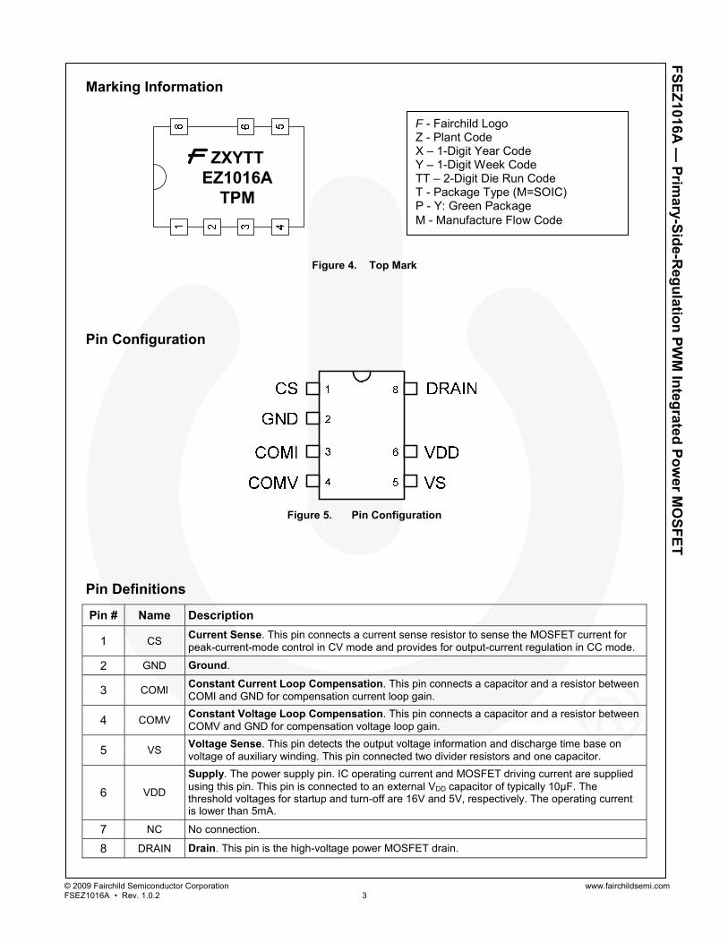
1 CS Current Sense. This pin connects a current sense resistor to sense the MOSFET current for peak-current-mode control in CV mode and provides for output-current regulation in CC mode.
2 GND Ground.
3 COMI Constant Current Loop Compensation. This pin connects a capacitor and a resistor between COMI and GND for compensation current loop gain.
4 COMV Constant Voltage Loop Compensation. This pin connects a capacitor and a resistor between COMV and GND for compensation voltage loop gain.
5 VS Voltage Sense. This pin detects the output voltage information and discharge time base on voltage of auxiliary winding. This pin connected two divider resistors and one capacitor.
6 VDD
Supply. The power supply pin. IC operating current and MOSFET driving current are supplied using this pin. This pin is connected to an external VDD capacitor of typically 10µF. The threshold voltages for startup and turn-off are 16V and 5V, respectively. The operating current is lower than 5mA.
7 NC No connection.
8 DRAIN Drain. This pin is the high-voltage power MOSFET drain.
F - Fairchild Logo Z - Plant Code X – 1-Digit Year Code Y – 1-Digit Week Code TT – 2-Digit Die Run Code T - Package Type (M=SOIC) P - Y: Green Package M - Manufacture Flow Code
Absolute Maximum Ratings Stresses exceeding the absolute maximum ratings may damage the device. The device may not function or be operable above the recommended operating conditions and stressing the parts to these levels is not recommended. In addition, extended exposure to stresses above the recommended operating conditions may affect device reliability. The absolute maximum ratings are stress ratings only.
Symbol Parameter Min. Max. Unit VDD DC Supply Voltage(1,2) 30 V VVS VS Pin Input Voltage -0.3 7.0 V VCS CS Pin Input Voltage -0.3 7.0 V
VCOMV Voltage-Error Amplifier Output Voltage -0.3 7.0 V VCOMI Voltage-Error Amplifier Output Voltage -0.3 7.0 V
VDS Drain-Source Voltage 600 V
ID Continuous Drain Current TC=25°C 1.0 A TC=100°C 0.6 A
IDM Pulsed Drain Current 4 A EAS Single Pulse Avalanche Energy 33 mJ IAR Avalanche Current 1 A
PD Power Dissipation (TA<50°C) 660 mW
ΘJA Thermal Resistance (Junction-to-Air) 153 °C/W
ΘJC Thermal Resistance (Junction-to-Case) 39 °C/W
TJ Operating Junction Temperature -40 +150 °C TSTG Storage Temperature Range -55 +150 °C TL Lead Temperature (Wave Soldering or IR, 10 Seconds) +260 °C
ESD Electrostatic Discharge Capability
Human Body Model, JEDEC: JESD22-A114
2 kV
Charged Device Model, JEDEC: JESD22-C101
2
Notes: 1. Stresses beyond those listed under Absolute Maximum Ratings may cause permanent damage to the device. 2. All voltage values, except differential voltages, are given with respect to GND pin.
Recommended Operating Conditions The Recommended Operating Conditions table defines the conditions for actual device operation. Recommended operating conditions are specified to ensure optimal performance to the datasheet specifications. Fairchild does not recommend exceeding them or designing to Absolute Maximum Ratings.
Symbol Parameter Conditions Min. Typ. Max. Unit TA Operating Ambient Temperature -40 +125 °C
Electrical Characteristics VDD=15V and TA=-40°C~+125°C (TA=TJ), unless otherwise specified.
Symbol Parameter Conditions Min. Typ. Max. UnitsVDD Section
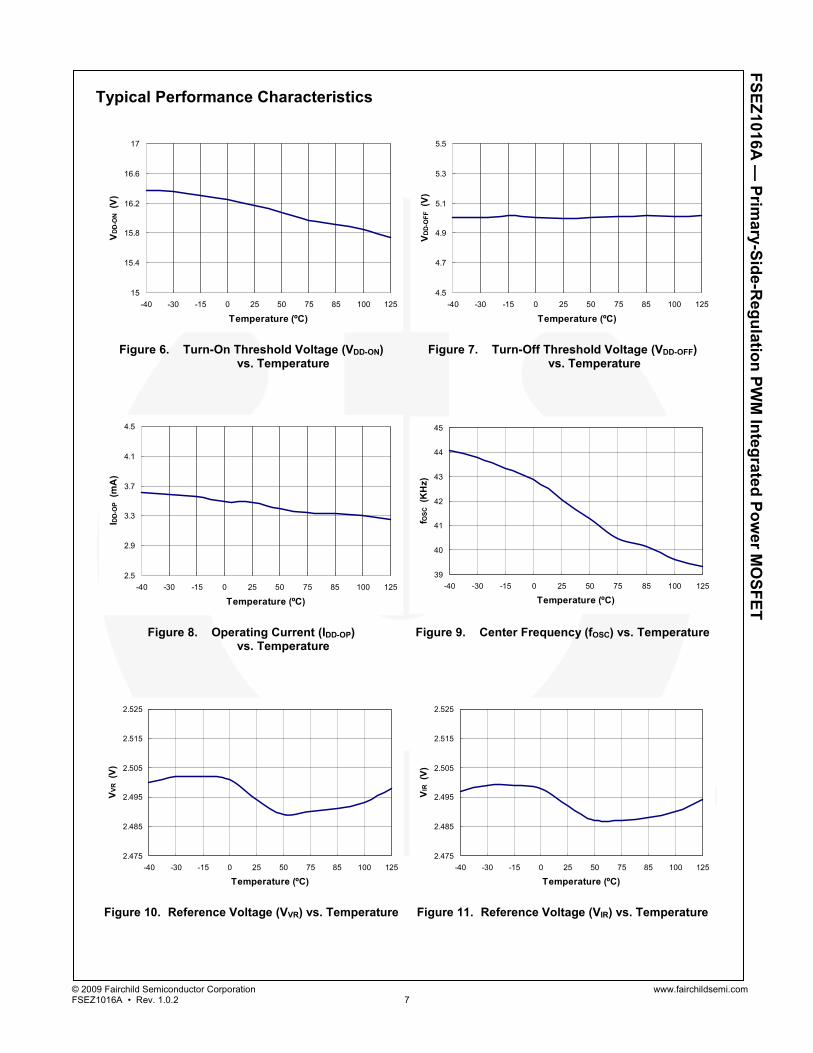
VOP Continuously-Operating Voltage 25 V VDD-ON Turn-On Threshold Voltage 15 16 17 V VDD-OFF Turn-Off Threshold Voltage 4.5 5.0 5.5 V IDD-ST Startup Current 0<VDD<VDD-ON-0.16V 3.7 10.0 μA
IDD-OP Operating Current VDD=20V, fS= fOSC VVS=2V, VCS=3V CL=1nF
3.5 5.0 mA
IDD-GREEN Green Mode Operating Supply Current VDD=20V, VVS=2.7V CL=1nF, VCOMV=0V fS=fOSC-N-MIN, VCS=0V
Functional DescriptionFigure 24 shows the basic circuit diagram of a primary-side regulated flyback converter, with typical waveforms shown in Figure 25. Generally, discontinuous conduction mode (DCM) operation is preferred for primary-side regulation because it allows better output regulation. The operation principles of DCM flyback converter are as follows:
During the MOSFET ON time (tON), input voltage (VDL) is applied across the primary-side inductor (Lm). Then MOSFET current (Ids) increases linearly from zero to the peak value (Ipk). During this time, the energy is drawn from the input and stored in the inductor.
When the MOSFET is turned off, the energy stored in the inductor forces the rectifier diode (D) to turn on. While the diode is conducting, the output voltage (VO), together with diode forward-voltage drop (VF), are applied across the secondary-side inductor (Lm×Ns
2/ Np
2) and the diode current (ID) decreases linearly from the peak value (Ipk× Np/Ns) to zero. At the end of inductor current discharge time (tDIS), all the energy stored in the inductor has been delivered to the output.
When the diode current reaches zero, the transformer auxiliary winding voltage (VW) begins to oscillate by the resonance between the primary-side inductor (Lm) and the effective capacitor loaded across MOSFET.
During the inductor current discharge time, the sum of output voltage and diode forward-voltage drop is reflected to the auxiliary winding side as (VO+VF)× NA/NS. Since the diode forward-voltage drop decreases as current decreases, the auxiliary winding voltage reflects the output voltage best at the end of diode conduction time where the diode current diminishes to zero. By sampling the winding voltage at the end of the diode conduction time, the output voltage information can be obtained. The internal error amplifier for output voltage regulation (EA_V) compares the sampled voltage with internal precise reference to generate error voltage (VCOMV), which determines the duty cycle of the MOSFET in CV mode.
Meanwhile, the output current can be estimated using the peak drain current and inductor current discharge time since output current is the same as the average of the diode current in steady state.
The output current estimator detects the peak value of the drain current by a peak detection circuit and calculates the output current by the inductor discharge time (tDIS) and switching period (tS). This output information is compared with the internal precise reference to generate error voltage (VCOMI), which determines the duty cycle of the MOSFET in CC mode. With Fairchild’s innovative technique TRUECURRENT™, constant current (CC) output can be precisely controlled.
Of the two error voltages, VCOMV and VCOMI, the smaller determines the duty cycle. During constant voltage regulation mode, VCOMV determines the duty cycle while VCOMI is saturated to HIGH. During constant current
regulation mode, VCOMI determines the duty cycle while VCOMV is saturated to HIGH.
+VDL
-
Lm
+
VO
-
Np:Ns
Ids
IDD
Primary-Side RegulationController
+Vw-
VDD
VS
CS
+ VF -
NA
LOAD
IO
IOEstimator
VOEstimator
t DISDetector
PWMControl
RCS
VAC
Ref
RefEA_V
EA_I
VCOMV
VCOMI
RS1
RS2
Figure 24. Simplified PSR Flyback Converter Circuit
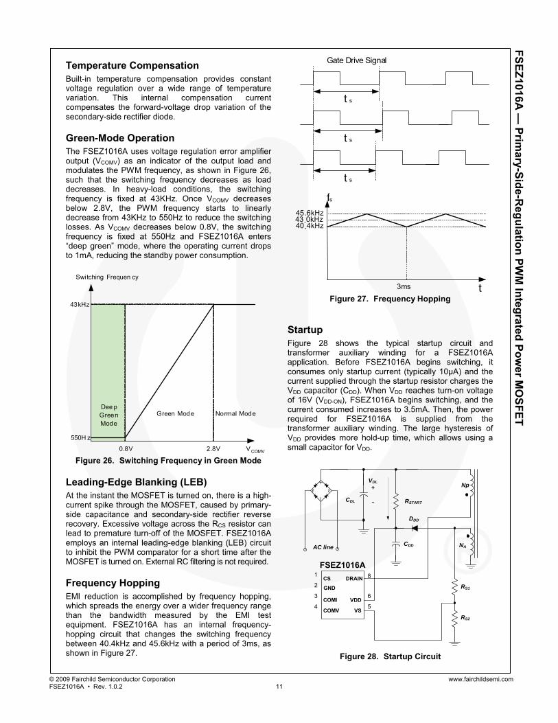
Temperature Compensation Built-in temperature compensation provides constant voltage regulation over a wide range of temperature variation. This internal compensation current compensates the forward-voltage drop variation of the secondary-side rectifier diode.
Green-Mode Operation The FSEZ1016A uses voltage regulation error amplifier output (VCOMV) as an indicator of the output load and modulates the PWM frequency, as shown in Figure 26, such that the switching frequency decreases as load decreases. In heavy-load conditions, the switching frequency is fixed at 43KHz. Once VCOMV decreases below 2.8V, the PWM frequency starts to linearly decrease from 43KHz to 550Hz to reduce the switching losses. As VCOMV decreases below 0.8V, the switching frequency is fixed at 550Hz and FSEZ1016A enters “deep green” mode, where the operating current drops to 1mA, reducing the standby power consumption.
Figure 26. Switching Frequency in Green Mode
Leading-Edge Blanking (LEB) At the instant the MOSFET is turned on, there is a high-current spike through the MOSFET, caused by primary-side capacitance and secondary-side rectifier reverse recovery. Excessive voltage across the RCS resistor can lead to premature turn-off of the MOSFET. FSEZ1016A employs an internal leading-edge blanking (LEB) circuit to inhibit the PWM comparator for a short time after the MOSFET is turned on. External RC filtering is not required.
Frequency Hopping EMI reduction is accomplished by frequency hopping, which spreads the energy over a wider frequency range than the bandwidth measured by the EMI test equipment. FSEZ1016A has an internal frequency-hopping circuit that changes the switching frequency between 40.4kHz and 45.6kHz with a period of 3ms, as shown in Figure 27.
Figure 27. Frequency Hopping
Startup Figure 28 shows the typical startup circuit and transformer auxiliary winding for a FSEZ1016A application. Before FSEZ1016A begins switching, it consumes only startup current (typically 10μA) and the current supplied through the startup resistor charges the VDD capacitor (CDD). When VDD reaches turn-on voltage of 16V (VDD-ON), FSEZ1016A begins switching, and the current consumed increases to 3.5mA. Then, the power required for FSEZ1016A is supplied from the transformer auxiliary winding. The large hysteresis of VDD provides more hold-up time, which allows using a small capacitor for VDD.
Protections The FSEZ1016A has several self-protective functions, such as Over-Voltage Protection (OVP), Over-Temperature Protection (OTP), and brownout protection. All the protections are implemented as auto-restart mode. When the auto-restart protection is triggered, switching is terminated and the MOSFET remains off. This causes VDD to fall. When VDD reaches the VDD turn-off voltage of 5V, the current consumed by FSEZ1016A reduces to the startup current (maximum 10µA) and the current supplied startup resistor charges the VDD capacitor. When VDD reaches the turn-on voltage of 16V, FSEZ1016A resumes normal operation. In this manner, the auto-restart alternately enables and disables the switching of the MOSFET until the fault condition is eliminated (see Figure 29).
FaultSituation
5V
16V
VDD
VDS
FaultOccurs
Fault Removed
NormalOperation
NormalOperation
PowerOn
Operating Current
3.5mA
10µA
Figure 29. Auto-Restart Operation
VDD Over-Voltage Protection (OVP) VDD over-voltage protection prevents damage from over-voltage conditions. If the VDD voltage exceeds 28V by open-feedback condition, OVP is triggered. The OVP has a debounce time (typical 250µs) to prevent false triggering by switching noise. It also protects other switching devices from over voltage.
Over-Temperature Protection (OTP) A built-in temperature-sensing circuit shuts down PWM output if the junction temperature exceeds 140°C.
Brownout Protection FSEZ1016A detects the line voltage using auxiliary winding voltage since the auxiliary winding voltage reflects the input voltage when the MOSFET is turned on. The VS pin is clamped at 1.15V while the MOSFET is turned on and brownout protection is triggered if the current out of the VS pin is less than IVS-UVP (typical 180μA) during the MOSFET conduction.
Pulse-by-Pulse Current Limit When the sensing voltage across the current sense resistor exceeds the internal threshold of 1.3V, the MOSFET is turned off for the remainder of the switching cycle. In normal operation, the pulse-by-pulse current limit is not triggered since the peak current is limited by the control loop.
NOTES: A) THIS PACKAGE CONFORMS TO JEDEC MS-012 VARIATION AA EXCEPT FOR MISSING PIN 7. B) ALL DIMENSIONS ARE IN MILLIMETERS. C) DIMENSIONS DO NOT INCLUDE MOLD FLASH OR BURRS. D) DRAWING FILENAME: M07AREV2
Package drawings are provided as a service to customers considering Fairchild components. Drawings may change in any manner without notice. Please note the revision and/or date on the drawing and contact a Fairchild Semiconductor representative to verify or obtain the most recent revision. Package specifications do not expand the terms of Fairchild’s worldwide terms and conditions, specifically the warranty therein, which covers Fairchild products. Always visit Fairchild Semiconductor’s online packaging area for the most recent package drawings: http://www.fairchildsemi.com/packaging/.