Page 1
Fully Differential Difference Amplifier based Microphone Interface Circuit and
an Adaptive Signal to Noise Ratio Analog Front end for Dual Channel Digital
Hearing Aids.
by
Syed Roomi Naqvi
A Dissertation Presented in Partial Fulfillment
of the Requirements for the Degree
Doctor of Philosophy
Approved May 2011 by the
Graduate Supervisory Committee:
Sayfe Kiaei, Chair
Bertan Bakkaloglu
Junseok Chae
Hugh Barnaby
James Aberle
ARIZONA STATE UNIVERSITY
August 2011
Page 2
ii
ABSTRACT
A dual-channel directional digital hearing aid (DHA) front-end using a fully
differential difference amplifier (FDDA) based Microphone interface circuit
(MIC) for a capacitive Micro Electro Mechanical Systems (MEMS) microphones
and an adaptive-power analog font end (AFE) is presented.
The Microphone interface circuit based on FDDA converts the capacitance
variations into voltage signal, achieves a noise of 32 dB SPL (sound pressure
level) and an SNR of 72 dB, additionally it also performs single to differential
conversion allowing for fully differential analog signal chain. The analog front-
end consists of 40dB VGA and a power scalable continuous time sigma delta
ADC, with 68dB SNR dissipating 67uW from a 1.2V supply. The ADC
implements a self calibrating feedback DAC, for calibrating the 2nd
order non-
linearity. The VGA and power scalable ADC is fabricated on 0.25 um CMOS
TSMC process.
The dual channels of the DHA are precisely matched and achieve about 0.5dB
gain mismatch, resulting in greater than 5dB directivity index. This will enable a
highly integrated and low power DHA.
Page 3
iii
DEDICATION
I dedicate this work to the continuous encouragement of my parents especially my
father to complete this work. To my wife and children for their patience in
enduring through this decade long process.
Page 4
iv
ACKNOWLEDGMENTS
I want to specially acknowledge the infinite patience shown by Sayfe Kiaei, for
allowing me to complete this work. He continuously nudged and prodded me to
complete and readily allowed me to work around my crazy life schedule. Without
his patience, I would not have been able to complete this.
I would also like to thank my sister-in-law Nida Tanveer for helping with MS
WORD related questions.
Page 5
v
TABLE OF CONTENTS
Page
LIST OF TABLES .......................................................................................................... viii
LIST OF FIGURES .......................................................................................................... ix
1. INTRODUCTION ....................................................................................................... 1
1.1. A brief Overview of Digital Hearing Aid System Architectures and
Issues .......................................................................................... 2
1.2. Proposed Directional Digital Hearing Aid System Architectures ...... 8
1.3. Contributions: FDDA based MEMS interface Circuit, self calibrating
DAC for an adaptive power scaling ADC. ..................................................... 14
1.4. Thesis Outline ..................................................................................... 14
2. SYSTEM ARCHITECTURE FOR MEMS MICROPHONE INTERFACE.......... 15
2.1. Overview of the MEMS Interface System Architecture ................... 15
2.2. CMOS MEMs Microphone ............................................................... 16
2.3. MEMs Microphone Behavioral Model ............................................. 19
3. OVERVIEW OF SENSING CAPACITANCE ARCHITECTURES ..................... 23
3.1. Overview of Capacitive Sensing Architectures ................................. 23
3.2. Proposed MEMS Microphone Interface Architecture ...................... 25
3.2.1. CTV Architecture Based on FDDA .............................25
3.2.2. Fully Differential Difference Amplifier(FDDA) .........28
3.2.3. Microphone Interface System Analysis .......................33
Page 6
vi
Chapter ................................................................................. Page
3.2.4. Microphone Interface Simulation Results ...................33
3.2.5. MEMs Microphone and MEMs Interface Noise
Analysis........................................................................36
4. ANALOG FRONT END ARCHITECTURE AND CIRCUIT ............................... 38
4.1. Analog Front End(AFE) Architecture Overview .............................. 38
4.2. Variable Gain Amplifier Design ........................................................ 39
4.3. 4th
-order CT Σ∆ ADC Architecture ................................................... 44
4.3.1. Behavioral Model of the 4th
-order CT Σ∆ ....................47
4.3.2. Amplifier Non-idealities ..............................................49
4.3.3. Feedback DAC Non-idealities ....................................52
4.3.4. Clock Jitter and Excess Loop Delay ............................52
4.4. 4th
-order CT Σ∆ ADC Circuit Design ................................................ 56
4.4.1. 4th
order CT Loop Filter Design ..................................56
4.4.1.1.1. Input Stage Active RC integrator ............................56
4.4.1.2. gm-C integrator ............................................................57
4.4.1.3. Design gm-C integrator for the NTF Zero ...................58
4.4.2. Quantizer Design .........................................................60
4.5. Proposed Feedback DAC Architecture............................................. 62
4.5.1. First Feedback Design and Self Calibration ................64
4.5.1. Other Feedback DAC Design .....................................73
5. TEST SETUP AND MEASUREMENT RESULTS................................................ 76
6. CONCLUSION AND FUTURE WORKS ............................................................... 82
Page 7
vii
Chapter ................................................................................. Page
REFERENCES ................................................................................................................ 83
Page 8
viii
LIST OF TABLES
Table Page
1: Typical architectural requirements for Digital Hearing Aids .............................8
2: Noise parameters for the Audio Signal Chain ..................................................11
3: Block Specifications for the DHA ...................................................................13
4: CMOS MEMS Microphone Characteristics ....................................................17
5: FDDA Noise Summary Report ........................................................................36
6: Coefficients of the proposed loop filter ...........................................................46
Page 9
ix
LIST OF FIGURES
Figure Page
1: A Typical Digital Hearing System......................................................................2
2: A Polar plot of two directional microphones with mismatch in the audio signal
path ...........................................................................................................................5
3. Power spectral density of the noise floor in a quite environment. ......................6
4: Power spectral density of the noise floor in noisy environment. .......................7
5: The proposed dual channel DHA Architecture ..................................................9
6: The audio signal chain from input sound pressure in dB SPL to digital bits ..11
7. MEMS Microphone and Preamplifier. ............................................................15
8. 3D view of the MEMS Capacitive Microphone ..............................................17
9. Microphone capacitance change with respect to DC bias. ...............................18
10. Acoustic characterization curve of the MEMS microphone ...........................19
11. Parallel Plate representation of a MEMS Microphone ...................................20
12. First order Electrical Model of the MEMs Microphone .................................22
13. Output response of the MEMs variable cap model .........................................22
14. FDDA based MEMS interface circuit............................................................27
15. Block diagram of a fully differential difference amplifier..............................29
16. Schematic of the Fully differential difference amplifier .................................31
17:. FDDA open loop gain and phase margin simulation results .........................32
18. Dynamic Range Simulation Results ...............................................................34
19. . THD of the differential output @ 1.05kHz ...................................................34
Page 10
x
Figure Page
20. Transient Simulation Results of the Full Signal Path including the VGA with
105 dB SPL input ...................................................................................................35
21. Block diagram of the Analog Front End .........................................................38
22. Gain curves for the VGA for the three different power/SNR settings. ...........40
23. Block diagram of the VGA, MRC and the feedback resistor .........................41
24. VGA output Noise Scaling for different values of the Feedback resistor, .....42
25. Class B OTA for the VGA .............................................................................43
26. Block diagram of the 4th
order CT sigma delta ..............................................46
27. Power Spectral density plot of the ideal 4th
order CT Sigma Delta ...............47
28 Coefficient Sensitivity Analysis .....................................................................48
29. Block diagram of the Σ∆ ADC with Macro models for the opamp and DAC50
30. SQNR degradation Vs the gain of the Amp Active RC amplifier varies ......51
31:, Modeling the effect of clock jitter on the DAC Current pulse ......................52
32:, Matlab Simulation showing the impact of jitter on the SNR of the ADC .....54
33. Clock waveforms depicting the excess loop delay impact on RZ DAC vs
NRZ DAC ..............................................................................................................55
34:, Fully differential folded cascode opamp used in the Active RC integrator. ..58
35:, Fully differential folded cascode gm used in the gm-C integrator. .............59
36:, Fully differential folded cascode gm used in the local zero gm-C integrator59
37. 3- level Quantizer and Schematic of the comparator .....................................61
38. Timing diagram of the Quantizer ...................................................................62
Page 11
xi
Figure Page
39 A high level representation of the proposed feedback DAC Architecture .....63
40 Basic Self Calibration Scheme........................................................................66
41 Proposed Self Calibration Scheme..................................................................68
42. Schematic diagram of the first DAC ...............................................................69
43. Feedback DAC input referred noise ...............................................................70
44. Feedback DAC1 SNR for different current settings ......................................71
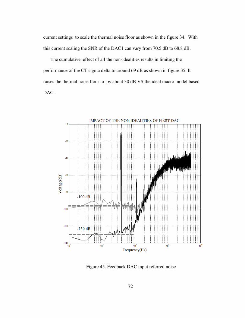
45. Feedback DAC input referred noise ...............................................................72
46. Schematic diagram of the other feedback DACs (2,3 &4) .............................73
47. Transient simulations of the common mode keeper showing the glitches
being generated in the zero state . ..........................................................................74
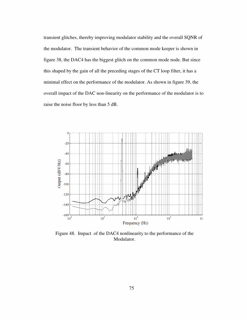
48. Impact of the DAC4 nonlinearity to the performance of the Modulator. .....75
49. Test setup for measurement and evaluation of the DHA/ SD ADC ...............76
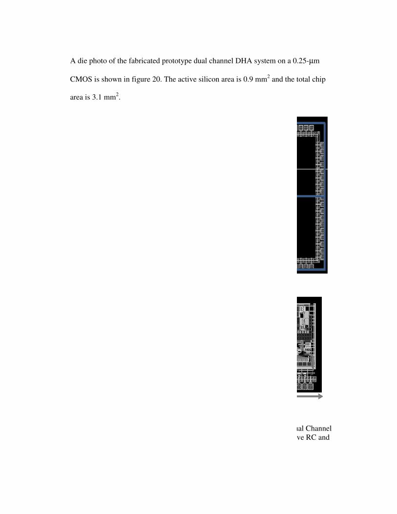
50. Die photos of the DHA System depicting the (a) The Dual Channel
Implementation (b) Single channel details showing the VGA, Active RC and
DACs......................................................................................................................77
51: Measured SNR in dB Vs input Signal Amplitude. ........................................79
52: Measured transfer curve of the Sigma Delta ADC showing no peaking and
channel gain flatness. .............................................................................................79
53: Measured transfer curve of the Sigma Delta ADC showing no peaking and
channel gain flatness. .............................................................................................80
Page 12
xii
Figure Page
54: Measured 2nd
order harmonic distortion of a) without calibration enabled b)
with calibration enabled. ........................................................................................81
Page 13
1
CHAPTER 1
1. INTRODUCTION
Hearing loss afflicts approximately 10% of the world population;
the basic solution is amplification of sound to compensate for acoustic
signal loss in the ear. Hearings aids can be either analog or digital, with
the current advances in digital chip design and digital signal processing
technologies, digital hearing aids have become prevalent. One of the
fundamental challenges for hearing impaired is speech intelligibility in
presence of background noise. The ability to understand speech in a
noisy background is expressed as signal-to-noise ratio for comprehending
50% for speech namely SNR-50. In hearing impaired the SNR-50 could be
as much as 30dB higher than normal people to achieve the same level of
speech comprehension [1]. As such background noise reduction and
increasing speech intelligibility is a key challenge for hearing aid design.
This thesis presents the implementation and characterization details of a
dual channel analog front-end (AFE) for digital hearing aid (DHA)
applications that uses novel Micro Electro-Mechanical Systems (MEMS)
audio transducers and ultra-low power scalable A/D converters, which
enable a very-low form factor, energy-efficient implementation for next
generation DHA. The key contribution of the thesis is the implementation
of the MEMS microphone interface circuit and power scalable Σ∆ ADC
system with self calibrating feedback DAC.
Page 14
2
1.1. A brief Overview of Digital Hearing Aid System
Architectures and Issues
The first generation of hearing aids consisted of analog variable
gain amplifiers, electret microphones and speakers that compensated for
hearing loss. These hearing aids dissipated a considerable amount of
power and had flat frequency characteristics that made these devices
uncomfortable for most patients. Human hearing and speech sensitivity of
human ear is non uniform across the audio frequency band and as such
the human hearing loss also varies non uniformly with frequency[1]. The
next generation of devices adopted analog filter banks in which band-pass
filters were used in parallel to amplify the acoustic signal to a specific
level in each different frequency band. This design, however, resulted in
bulky devices that still required high power consumption [2]. A major
breakthrough was achieved through the development of DHAs that
exploited the power of digital signal processors (DSPs) that allowed full
programmability and customization to a patient’s hearing characteristic [3-
7].
Figure 1: A Typical Digital Hearing System
Page 15
3
A typical single channel DHA system, shown in Fig. 1, consists of
a Microphone interface circuit, an analog front end (AFE), DSP, followed
by digital to analog (DAC) converter and a speaker driver. The AFE
consists of a Variable Gain Amplifier (VGA) and an Analog to Digital
Converter (ADC). The receiver front end receives the processed digital
signal from DSP and converts it to the analog domain. At the backend, a
speaker delivers the acoustic sound to excite the patient’s eardrums. The
current generation DHA’s employ microphone arrays combined with
adaptive array processing that improve audio quality and perception in
real-life environments through noise cancellation mechanisms. Such
directional DHAs exploit the use of multiple microphone arrays (MMAs)
to provide the patient with information on the spatial position of the
desired acoustic source, while attenuating the ambient noise at the same
time [8]. MMAs apply adaptive beam forming techniques to estimate the
signal direction and cancel ambient noise [9-10]. Such directional gain
enhancement is quantified through the directivity index (DI). In short
directivity index is a measure of the directionality of a MMA system
which is measure of speech intelligibility by enhancing the gain of the
signal coming from the direction of the desired source, while suppressing
noise from other directions. Directivity index is given by eq 1. 1
Page 16
4
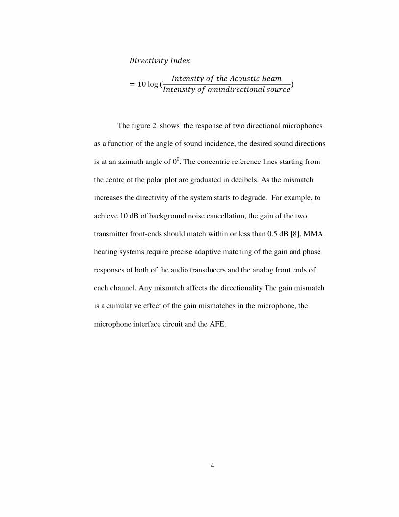
= 10 log ( ℎ )
The figure 2 shows the response of two directional microphones
as a function of the angle of sound incidence, the desired sound directions
is at an azimuth angle of 00. The concentric reference lines starting from
the centre of the polar plot are graduated in decibels. As the mismatch
increases the directivity of the system starts to degrade. For example, to
achieve 10 dB of background noise cancellation, the gain of the two
transmitter front-ends should match within or less than 0.5 dB [8]. MMA
hearing systems require precise adaptive matching of the gain and phase
responses of both of the audio transducers and the analog front ends of
each channel. Any mismatch affects the directionality The gain mismatch
is a cumulative effect of the gain mismatches in the microphone, the
microphone interface circuit and the AFE.
Page 17
5
Figure 2: A Polar plot of two directional microphones with
mismatch in the audio signal path
The dynamic range and power level of an audio signal have
different characteristics in different environments. As illustrated in Fig.
2(a), the audio spectrum of a conversation in quiet environments shows
that the noise floor is at about 0 dB-SPL (dB Sound Pressure Level), and
the acoustic signal has a 65-dB dynamic range. Fig 2(b) shows the
spectrum of the same conversation in a noisy environment (i.e., street)
where the noise floor has increased to 25 dB-SPL and the dynamic range
is now only 55 dB. Clearly, to cope with the ambient noise, the person
who is speaking raises his voice level, but only up to the level of
comfortable hearing.l. Consequently, it is clear that changes in signal
power, dynamic range and noise floor – can all be exploited to optimize
the AFE circuit power consumption. In fact, in high background noise
Page 18
environments, the DHA system can decide to relax the front
performance and optimize its parameters to avoid degradation (i.e.,
clipping) of the high sound
architectures have a fixed front
dB) to cope with different ambient noise condition
power consumption.
Figure
6
environments, the DHA system can decide to relax the front-end noise
e and optimize its parameters to avoid degradation (i.e.,
clipping) of the high sound-level desired signal. Conventional hearing aid
architectures have a fixed front-end dynamic range (e.g., as high as 120
dB) to cope with different ambient noise conditions but require high
power consumption.
Figure 3. Power spectral density of the noise floor in a quite
environment.
end noise
e and optimize its parameters to avoid degradation (i.e.,
Conventional hearing aid
end dynamic range (e.g., as high as 120
s but require high
oise floor in a quite
Page 19
Figure
The existing DHAs are plagued with three major issues namely
1. The quick degradation of performance in noisy
environments in which the AFE becomes saturated due to the ambient
acoustic content and background noise. Background noise interferes with
the desired conversation thereby impairing intelligibility.
a very high dynamic range AFE can help relieving this problem, it comes
at the expense of high power consumption and complexity.
2. The cumulative gain mismatch in the audio signal path in
case of multiple microphone based implementation used in directional
DHA’s , degrades the directionality that can be achieved.
3. In current DHA’
electret microphones; however their large size prohibits the application of
7
Figure 4: Power spectral density of the noise floor in
environment.
ing DHAs are plagued with three major issues namely
The quick degradation of performance in noisy
environments in which the AFE becomes saturated due to the ambient
acoustic content and background noise. Background noise interferes with
ersation thereby impairing intelligibility. While the use of
a very high dynamic range AFE can help relieving this problem, it comes
at the expense of high power consumption and complexity.
The cumulative gain mismatch in the audio signal path in
multiple microphone based implementation used in directional
DHA’s , degrades the directionality that can be achieved.
In current DHA’s the most widely used microphones are
electret microphones; however their large size prohibits the application of
r in noisy
ing DHAs are plagued with three major issues namely
environments in which the AFE becomes saturated due to the ambient
acoustic content and background noise. Background noise interferes with
While the use of
a very high dynamic range AFE can help relieving this problem, it comes
The cumulative gain mismatch in the audio signal path in
multiple microphone based implementation used in directional
the most widely used microphones are
electret microphones; however their large size prohibits the application of
Page 20
8
MMA techniques in completely in-the-ear-canal systems, plus they tend to
exhibit a high level of gain mismatch severely impacting the directivity
index.
1.2. Proposed Directional Digital Hearing Aid System
Architectures
The proposed architecture adapts to noise floor conditions by
adjusting system linearity and SNR of the Analog Front-End (AFE) to
maintain optimal performance. This architecture can optimize power
consumption depending on the ambient conditions, thereby maximizing
battery life. However, changing the system architecture to scale SNR can
lead to transient artifacts, such as clicks or pops, or potential system
instability. These issues have been also addressed in this work. The design
requirements for a typical hearing aid are summarized in Table I
Table 1: Typical architectural requirements for Digital Hearing Aids
Parameters Value
Frequency Range 300Hz to 10KHz
Input Amplitude 0 to 120 dB SPL
Dynamic Range 120 dB
Harmonic Distortion
Input Amplitude < 80 dB SPL < 0.001% (60 dB)
Input Amplitude > 80 dB SPL < 0.01% (40 dB)
Equivalent Input Noise Level 29 dB SPL
Area/Size Small
Power Source 1.2 V supplied by zinc-air
cell based battery
Page 21
9
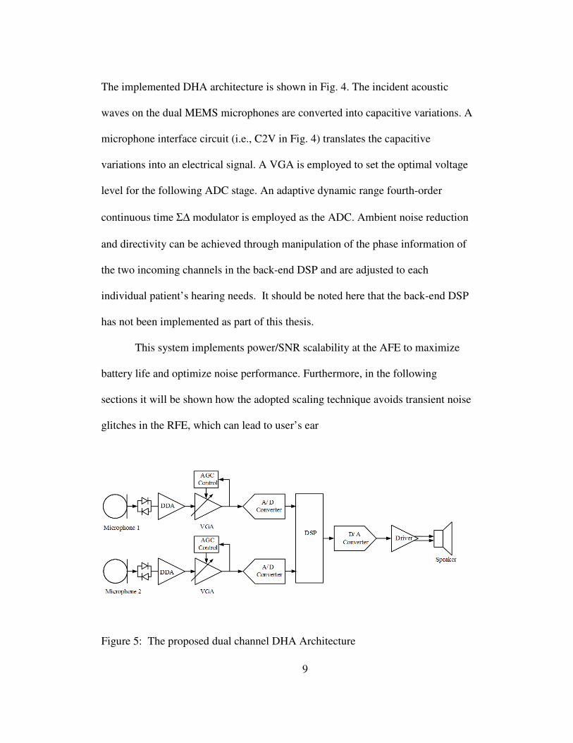
The implemented DHA architecture is shown in Fig. 4. The incident acoustic
waves on the dual MEMS microphones are converted into capacitive variations. A
microphone interface circuit (i.e., C2V in Fig. 4) translates the capacitive
variations into an electrical signal. A VGA is employed to set the optimal voltage
level for the following ADC stage. An adaptive dynamic range fourth-order
continuous time Σ∆ modulator is employed as the ADC. Ambient noise reduction
and directivity can be achieved through manipulation of the phase information of
the two incoming channels in the back-end DSP and are adjusted to each
individual patient’s hearing needs. It should be noted here that the back-end DSP
has not been implemented as part of this thesis.
This system implements power/SNR scalability at the AFE to maximize
battery life and optimize noise performance. Furthermore, in the following
sections it will be shown how the adopted scaling technique avoids transient noise
glitches in the RFE, which can lead to user’s ear
Figure 5: The proposed dual channel DHA Architecture
Page 22
10
fatigue and hearing discomfort. It additionally implements a MEMS interface
circuit based on fully differential difference Amplifier (FDDA), which not only
converts the audio signal into electrical (voltage) but also provides a single-
ended to differential conversion.
The audio signal which is essentially sound waves causing a change in the
atmospheric pressure around its mean value. This variation in atmospheric
pressure is transduced by the MEMS microphone into capacitance changes which
are in turn converted to voltage by the FDDA based interface circuit. The
voltage signal then gets amplified by the VGA to optimum amplitude level to
achieve the maximum dynamic range for the ADC. The amplified signal is
oversampled by a Σ∆ AD and converted into 2-bit digital stream. This digital
signal is converted into 16-bit signal by a decimation filter which is processed by
the DSP. Each stage of this audio signal chain adds thermal and flicker noise to
the signal, while the ADC also adds quantization noise and the oscillator’s phase
noise is another source of degradation for the SNR. The audio signal chain is
designed in order to minimize the noise and maximize the SNR. The noise
affecting every stage is either thermal noise or flicker noise; while the microphone
is affected by mechanical/Brownian noise while since the BW of interest is from
300Hz to 10 KHz, the flicker noise tends to dominates. Fig 5 shows the full audio
signal chain which converts the input sound pressure in dB SPL to digital bits
with the additive noise input referred components at every stage. The quantization
noise (qnoise ) of the ADC and the phase noise (φnoise) of the clock source.
Page 23
11
Figure 6: The audio signal chain from input sound pressure in dB SPL to digital
bits
The input sound pressure level Psi has range from 0 to 120 dB SPL, while the
microphone sensitivity Smic is essentially the ratio of the capacitive change (δC)
over the nominal capacitance (Cmic) of the biased MEMs microphone expressed in
dBV/Pa. The parameters given in Figure 5 are defines as below
( ,"#$% ) output noise of the MEMs microphone
( ,&&'% ) input referred noise of the FDDA
( ,()'% ) input referred noise of the VGA
( ,'&$% ) input referred noise of the ADC
qnoise quantization noise.
Φnoise phase noise of the clock
Table 2: Noise parameters for the Audio Signal Chain
Page 24
12
Sound applied to a microphone is expressed as sound pressure level (SPL) with
reference to hearing threshold of human ear (Po = 20 .10-6
Pa) [2] which can be
expressed in decibels (dBSPL) as follows
* + , (*+,) = 20log (+.#+/ ) (1.2)
Where Psi is the sound pressure level incident on the microphone’s deflecting
membrane. To calculate resultant voltage signal, the dBSPL needs to be converted
to dBPa which is sound pressure level in decibels normalized to 1 Pascal (Pa)
given as follows
+ = *+, + 201 〖20 . 1034〗 + (1.3)
+ = *+, − 94 (1.4)
Now this sound pressure level incident on the microphone in terms of the absolute
pressure is converted to voltage as a function of the sensitivity of the microphone
(Smic) given as
8 = *+, − 94 + *"#$() (1.5)
The sensitivity of conventional electret microphones reported is around -44
dB/V/Pa [2], for the MEMS microphone used for the sensitivity is around the
same about -45 dBV/Pa refer to figure 9, in chapter 2. Hence the voltage out
(Vmo) of the microphone feeding into the microphone interface circuit and the
AFE is given as below
8"/ = 10&9:%; (1.6)
Page 25
13
The noise requirements at the input of the ADC are determined by the input signal
level which is a function of the input reference level which was set to -0.5V to
+0.5V, governed by the given below equation
<'&$ = 20log =# ,'&$ ,'&$% > (1.7)
Although the full audio dynamic range is 120 dB, but the useful hearable audio
dynamic range is about 65 dB.
Microphone Sensitivity (dBPa/V) -45.00
Sound Pressure Level (dBSPL) 0.00 120
Sound Pressure Level (dBPa) -94.00 26
Microphone Out(dBV)
-
139.00 -19
Microphone Out(V) 0.00 0.112
Blocks Values Units
Σ∆Σ∆Σ∆Σ∆ ADC
Input level (max) @ the ADC 0.50 V
Dynamic Range of ADC 70.00 dB
Total noise @ the input of ADC 55.90 uVrms
Vnoise 39.53 uVrms
VGA
VGA Gain 40.00 dB
VGA Input Noise 15.81 uVrms
FDDA MIC Circuit
FDDA Transducer Gain 6.00 dB
FDDA Input Noise 85.00 uVrms
FDDA Input Noise 12.57
dB
SPL
Signal to Noise Ratio 68.43
Table 3: Block Specifications for the DHA
Page 26
14
The full signal chain is able to achieve more than 65dB SNR which is required to
meet the comfort zone for audible sound as shown in figure 3.
1.3.Contributions: FDDA based MEMS interface Circuit, self calibrating
DAC for an adaptive power scaling ADC.
The contributions of this thesis are the development and implementation of
FDDA based MEMS microphone interface circuit based on C2V conversion, and
a self calibrating feedback DAC to for a power scalable ADC.
1.4.Thesis Outline
The rest of the thesis presents the implementation details of the proposed dual
channel Digital hearing Aid (DHA). Chapter 2 focuses on the system architecture
for the MEMS interface circuit design, which develops a MEMs microphone
behavioral model for designing the Fully differential difference amplifier
(FDDA). Chapter 3 presents the Analog front end architecture including the
Variable Gain Amplifier, the power scalable ADC, and the self calibrating
feedback DAC. Measurement setup and results are presented in chapter 4.
Chapter 5 presents the conclusions and future work.
Page 27
15
CHAPTER 2
2. SYSTEM ARCHITECTURE FOR MEMS MICROPHONE
INTERFACE
CMOS MEMS Microphone with their small size and ease of integration with
CMOS signal processing chain present opportunities for design of highly
integrated DHAs. Furthermore CMOS MEMS microphone are also becoming
increasing competitive in terms of price and performance with their electrets
counterparts. A CMOS MEMS microphone simply consists of a moveable plate
and a stiff back plate which forms a variable capacitor.
2.1.Overview of the MEMS Interface System Architecture
The proposed system consists of a MEMS microphone which is essentially
capacitive and low-noise low offset microphone preamplifier with a high input
impedance and balanced input. interface with a low noise The MEMS
microphone is biased by a DC voltage; the incident acoustic waves causes the
Figure 7. MEMS Microphone and Preamplifier.
Page 28
16
capacitance to vary which is converted to a voltage and amplified by the MIC
preamplifier as shown in Fig 7.
The preamplifier needs to have a very high input impedance to be able to
detect the acoustic signal without being affected by the impedance of the MEMs
microphone. A low input offset and low input referred noise is required to ensure
that the maximum gain can be used without getting swamped by the offset.
Additionally the input amplitude of the signal can vary from 20uV to 100mV with
at least SNR for about 14 dB.
2.2.CMOS MEMs Microphone
This section describes the MEMS microphone designed and developed by
the MEMS group at Arizona State University (ASU).. Fig. 3 depicts the
construction of the capacitive MEMS microphone that was used in the DHA
design. The device size is 2.5x2.5x0.5 mm3 and it consists of a multi layered
parylene diaphragm suspended over a silicon substrate [11-13]. This MEMS
microphone has three major parts the top and bottom electrodes which detect the
capacitance change, the Ag (anode) and the Ni(cathode) which are electrically
modulated as result of a phenomenon called electro deposition. The 1µm gap
between the diaphragm and substrate forms a parallel plate capacitor, where as the
sound pressure level causes a deflection in the diaphragm causing changes in the
capacitance. The substrate acts as the capacitor back plate and acoustic holes are
etched from the backside of the substrate to let the air in the gap move freely. This
MEMS microphone has the additionally property that its capacitance can be
Page 29
17
adjusted by applying a tuning voltage as a result of the electrochemical reaction
that takes place causing the movements of Ag+ ions.
This feature of the Microphone is used for tuning any gain mismatches in
two microphones. Fig. 5 shows the measured capacitance change as the DC
voltage bias is swept from 100 mV to 900 mV. When the DC bias voltage is in the
Figure 8. 3D view of the MEMS Capacitive Microphone
CMOS MEMS Microphone
Parameter Value Units
size 2.25x2.25x0.5 mm3
Capacitor Gap 1 um
Sensing Capacitance 20 pf
Capacitance Sensitivity 20 ff/mV
Table 4: CMOS MEMS Microphone Characteristics
Page 30
18
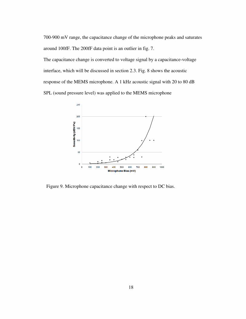
700-900 mV range, the capacitance change of the microphone peaks and saturates
around 100fF. The 200fF data point is an outlier in fig. 7.
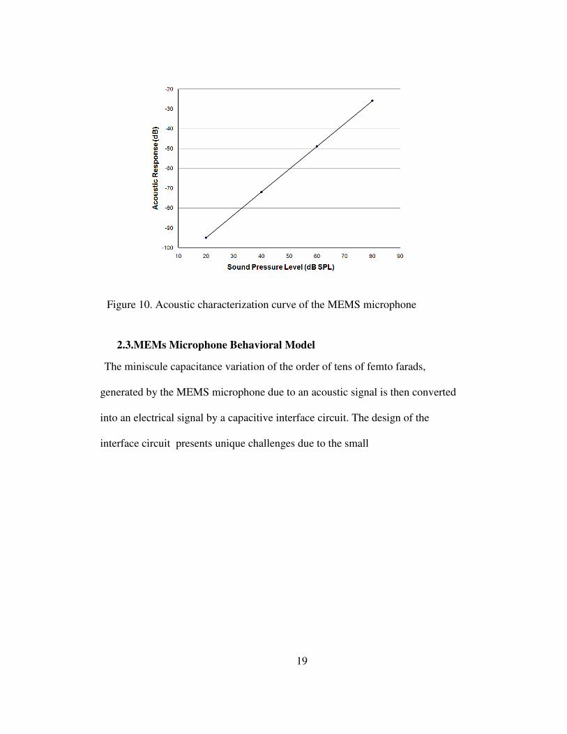
The capacitance change is converted to voltage signal by a capacitance-voltage
interface, which will be discussed in section 2.3. Fig. 8 shows the acoustic
response of the MEMS microphone. A 1 kHz acoustic signal with 20 to 80 dB
SPL (sound pressure level) was applied to the MEMS microphone
Figure 9. Microphone capacitance change with respect to DC bias.
Page 31
19
2.3.MEMs Microphone Behavioral Model
The miniscule capacitance variation of the order of tens of femto farads,
generated by the MEMS microphone due to an acoustic signal is then converted
into an electrical signal by a capacitive interface circuit. The design of the
interface circuit presents unique challenges due to the small
Figure 10. Acoustic characterization curve of the MEMS microphone
Page 32
20
sensing capacitance, the high output impedance, robust DC bias requirements, and
circuit noise (mechanical and electrical).
A typical MEMS condenser microphone needs to be connected to a bias
voltage source through a high impedance [14]. To first order, the MEMS
microphone can be modeled as a variable capacitor. Sound pressure moves one
side of the parallel plate capacitor, creating a capacitance change, as given in the
Figure 9.
For a MEMS microphone biased by a DC voltage Vbias, the charge Q(t) vs.
voltage V(t) relationship of a capacitor CMIC(t) is expressed by
?() = @ABC()8() (2.1)
?() = @ABC_EC8F#'. + ∆@()8$() (2.2)
Figure 11. Parallel Plate representation of a MEMS Microphone
Page 33
21
Where CMIC is the total capacitance of the MEMS Microphone, while CMIC_DC is
the nominal capacitance value at certain bias Vbias. ∆C is the change capacitance
caused due to the acoustic excitation of the MEMS Microphone, Vc is the
electrical equivalent of the acoustic signal. The sensed voltage of a MEMS
microphone can be derived from (3), by applying the charge conservation law,
.H .H = ∆@()@ABC_EC + @I 8F#'. (2.3)
where Cp is the parasitic capacitance associated with interconnect etc. The
sensitivity of the MEMs microphone is given as below
* = 8F#'. ∆@()(@ABC + @I)∆+ (2.4)
where ∆P is the change in sound pressure in Pascal, whereas Sensitivity has the
units of dBV/Pascal
A basic electrical veriloga model was developed for the MEMS microphone
based on the characteristics of the microphone as depicted in the curves in Figure
7 & 8. This basic electrical model of the MEMs microphone consists of a fixed
capacitor CMIC_DC and a variable Capacitor Cv which is modulated by the sound
pressure level, while RN represents the electrical equivalent of the acoustical noise
of the microphone, and CP being the parasitic capacitors.
`
Page 34
22
For this model the acoustic noise is assumed to be minimal. Actual
measurements of the acoustic noise of the MEMS microphone is around 20
dBSPL. A detailed noise analysis is presented in the next chapter..
Figure 12. First order Electrical Model of the MEMs Microphone
Figure 13. Output response of the MEMs variable cap model
Generic Variable Cap Model
0
0.2
0.4
0.6
0.8
1
1.2
1.4
1.6
-2.50 -2.00 -1.50 -1.00 -0.50 0.00 0.50 1.00 1.50 2.00 2.50
Vctrl(V)
Cap
acit
ance (
pF
)
Page 35
23
CHAPTER 3
3. OVERVIEW OF CAPACITIVE SENSING ARCHITECTURES
3.1.Overview of Capacitive Sensing Architectures
Capacitive sensing converts mechanical displacement or motion of the surfaces
forming the capacitance into an electrical based signal like voltage or current or a
time based signal like frequency or time period. In this thesis we are focused on
electrical based schemes which can generate voltage or current as an output.
Capacitors can sense ac signals only, as such ac modulation sources are required
for capacitive sensing. Capacitive sensing generates an AM signal that needs to be
sampled or demodulated, to extract its envelop. Capacitive sensing can be single
ended or differential. Differential capacitive sensing has all the advantages
associated with differential signaling.
Capacitive sensing only uses the parallel-plate part of the total CMOS MEMS
capacitor as the useful part, while the fringe part adds to the parasitic capacitance.
The other major non Idealities for CMOS MEMS capacitive sensors are
Brownian Noise of the MEMS device
• Electronic/Circuit Noise
o 1/f noise
o Thermal noise
• Circuit offset
• Sensor Offset
• Undesirable Charging
• Parasitic Capacitance
Page 36
24
• Very High Impedance Sense node
In the case of a hearing aid, the frequency of interest is in the audio band from
300Hz to 10KHz,. As such the Capacitive Sensing architectures can be
categorized according to the current, charge or voltage signals they generate.
A. Continuous-time Current sensing (CTC)
Continuous time current sensing is essentially based on trans-impedance
amplifiers (TIA). The charges transfer across the plates of the MEMS capacitor
creates an ac current which can be sensed using a TIA.
B. Switched Capacitor Charge Integration (SCI)
Since capacitive sensing is based on the charge-voltage relationship of the sensed
capacitor, which is also the basic principle on which switch capacitor circuits are
based, hence there is a natural fit. The SC circuits provide a virtual ground and
robust dc biasing of the sensing node making the sensed signal insensitive to
parasitic capacitance and charging. Additionally the SC circuit also offers a
number of techniques for offset reduction such as correlated double sampling
(CDS). The major drawbacks of SC charge injection is the noise folding caused
by the sampling process, the thermal noise of the switches, and the kT/C noise of
the small sampling capacitors.
Page 37
25
C. Continuous –time Voltage sensing (CTV)
The CTV approach is based on a impedance conversion buffer, the capacitance
change is converted into a voltage signal by properly biasing the MEMS
microphone. This voltage change is than amplified and buffered by a voltage
amplifier. The key challenge in this design is the DC biasing of the very high
impedance MEMS microphone. This approach has superior noise performance to
the other two approaches.
3.2.Proposed MEMS Microphone Interface Architecture
3.2.1. CTV Architecture Based on FDDA
A CTV approach based on a fully differential difference amplifier (FDDA) [20-
22] is proposed in this thesis, which can be implemented in the same process as
the rest of the analog front end (Fig. 12). The microphone interface with its high
impedance, wide dynamic range of around of 100dB, low noise, a THD of at least
-57 dB presents unique challenges. As such a low noise, low-offset, microphone
amplifier with a high impedance and matched input is required. The input
matching in addition with the high CMRR helps reject any external interference.
Low noise and low input referred offset helps to maximize the signal at the output
of the preamplifier while the high input impedance keeps the out of the preamp
isolated from the acoustic input. A FDDA seems to be a very good candidate to
meet these requirements. The FDDA consists of dual differential input pairs,
namely, a primary and auxiliary pair. The primary pair is connected to the MEMS
Page 38
26
microphone, while the auxiliary pair forms a feedback loop. The primary pair and
the auxiliary pair implement a virtual short circuit, which provides the high input
impedance required for the MEMS microphone and a low output impedance to
drive the next stage. The CMRR for the FDDA as would be shown later solely
depends on the transistor with amplifier and not on resistor matching. The other
two concerns in terms of 1/f noise and offset are addressed by proper choice and
sizing of the input pair of the amplifier.
The back-to-back (D1 and D2) are needed to provide the high impedance between
the MEMS microphone and the bias voltage. These diodes turn on as the voltage
of the high impedance sense node drifts from the bias point thereby essentially
clamping the voltage of the sense node to the bias point. The size of these diodes
is chosen as such to trade off the shot noise with the high impedance requirement.
Other biasing schemes have also been presented in the literature which use
periodic reset pass gate to connect the bias voltage to the sense node, the periodic
reset ensures that sense node does not drift [21]. A dummy MEMS capacitor also
needs to be used for the purpose of converting the charge into a voltage. In our
scheme an identical MEMS cap is used for this purpose in order to minimize any
mismatches, which is biased similarly as the actual MEMS microphone.
Page 39
27
This scheme requires a digital counter for generating the periodic reset, increasing
complexity, additionally issues like clock feed thru, charge sharing and noise
folding would have to be taken care of. As such the simpler diode biasing scheme
has been chosen for this implementation. The major disadvantage of this scheme
is that the shot noise generated by the diodes could take a few second in the order
of 3-4s before becoming negligible. Due to complexity of this acoustic-electrical
system, architectural design and analysis becomes very cumbersome. To
circumvent this issue a behavioral electrical model of the MEMs microphone was
developed to be able to simulate the whole system in the electrical domain.
Figure 14. FDDA based MEMS interface circuit
Page 40
28
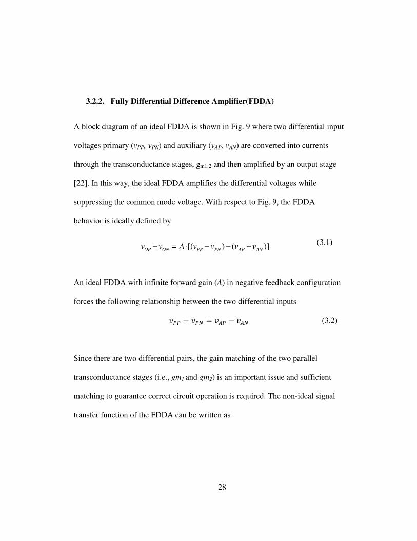
3.2.2. Fully Differential Difference Amplifier(FDDA)
A block diagram of an ideal FDDA is shown in Fig. 9 where two differential input
voltages primary (vPP, vPN) and auxiliary (vAP, vAN) are converted into currents
through the transconductance stages, gm1,2 and then amplified by an output stage
[22]. In this way, the ideal FDDA amplifies the differential voltages while
suppressing the common mode voltage. With respect to Fig. 9, the FDDA
behavior is ideally defined by
)]()[( ANAPPNPPONOP vvvvAvv −−−⋅=− (3.1)
An ideal FDDA with infinite forward gain (A) in negative feedback configuration
forces the following relationship between the two differential inputs
JJ − JK = LJ − LK (3.2)
Since there are two differential pairs, the gain matching of the two parallel
transconductance stages (i.e., gm1 and gm2) is an important issue and sufficient
matching to guarantee correct circuit operation is required. The non-ideal signal
transfer function of the FDDA can be written as
Page 41
29
ME = &[E − O8/PPO + 1@QQ<J (CJ − 8CJ;)+ 1@QQ<L (CL − 8CL; + 1@QQ<& (CE− 8CE;)
(3.3)
Where Ad and Voff are the differential gain and input referred offset, defined
similar to the case of conventional opamps. However, the CMMRP,A,d parameters
are unique to the FDDA due to the dual input pairs. The CMMRP and CMMRA are
the common mode rejection ratios of the primary and the auxiliary input pairs,
whereas the CMMRd is a measure of the difference of the differential inputs,
which also becomes a common mode signal, defined as
@Q<<& ≅ 11 − 1S1% (3.4)
Figure 15. Block diagram of a fully differential difference amplifier
Page 42
30
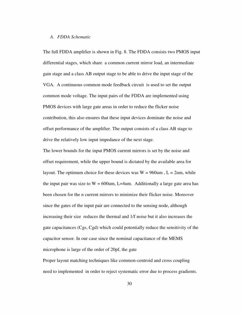
A. FDDA Schematic
The full FDDA amplifier is shown in Fig. 8. The FDDA consists two PMOS input
differential stages, which share a common current mirror load, an intermediate
gain stage and a class AB output stage to be able to drive the input stage of the
VGA. A continuous common mode feedback circuit is used to set the output
common mode voltage. The input pairs of the FDDA are implemented using
PMOS devices with large gate areas in order to reduce the flicker noise
contribution, this also ensures that these input devices dominate the noise and
offset performance of the amplifier. The output consists of a class AB stage to
drive the relatively low input impedance of the next stage.
The lower bounds for the input PMOS current mirrors is set by the noise and
offset requirement, while the upper bound is dictated by the available area for
layout. The optimum choice for these devices was W = 960um , L = 2um, while
the input pair was size to W = 600um, L=4um. Additionally a large gate area has
been chosen for the n current mirrors to minimize their flicker noise. Moreover
since the gates of the input pair are connected to the sensing node, although
increasing their size reduces the thermal and 1/f noise but it also increases the
gate capacitances (Cgs, Cgd) which could potentially reduce the sensitivity of the
capacitor sensor. In our case since the nominal capacitance of the MEMS
microphone is large of the order of 20pf, the gate
Proper layout matching techniques like common-centroid and cross coupling
need to implemented in order to reject systematic error due to process gradients.
Page 43
31
The choice of large gate areas of the input device and the current mirrors help to
minimize the process specific random errors. The total area of the preamplifier
comes out 0.076mm2
of active device area, with the area for the compensation
capacitors this will grow to 0.5 mm2
B. Simulation Results
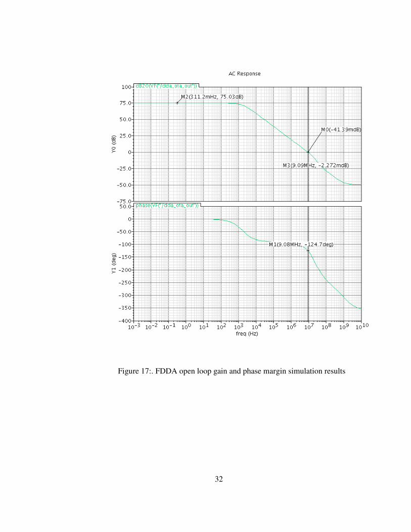
The FDDA has a DC gain of 75 dB, and GBW of 9MHz. Given below are the
simulation results for the Gain and phase.
Figure 16. Schematic of the Fully differential difference amplifier
Page 44
32
Figure 17:. FDDA open loop gain and phase margin simulation results
Page 45
33
3.2.3. Microphone Interface System Analysis
With the basic functionality of the FDDA established, let us go back and analyze
the interface circuit, From Fig 8, to calculate the small signal gain expression for
the interface circuit. The following two equations form the basis of the analysis
/TU = &[((8F#'. + .H .) − 8F#'.) − ( LJ − LK)] (3.5)
/TU = W &1 + X<%<SY &Z ( LJ − LK) (3.6)
Solving the above two equations in terms of vout and vsense, we get the following
/TU = &2 + X<%<SY & .H .
(3.7)
/TU = [<S<%\ .H . (3.8)
For a high enough differential gain, in our case of about 75 dB as shown the eq
(2.13) reduces to its classical version eq (2.14) in which gain is only a function of
the resistors R1 and R2. The above representations are ideal and are valid only
under the assumption of linearity; all the non-idealities have been assumed to be
negligible.
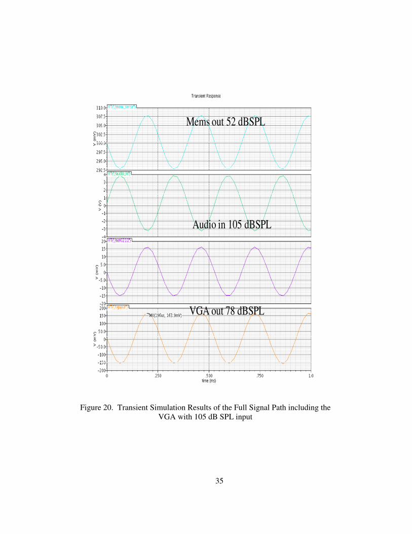
3.2.4. Microphone Interface Simulation Results
The interface circuit is expected to achieve more than 90 dB dynamic range as
shown in Fig 14. A plot of the simulated THD as a function of the input sound
Page 46
34
pressure in dBSPL @ 1.05 KHz is shown in Fig 15. The transient response of the
MEMS interface circuit including the including the VGA is shown in Fig 16.
Figure 18. Dynamic Range Simulation Results
Figure 19. THD of the differential output @ 1.05kHz
-60
-50
-40
-30
-20
-10
0
60 70 80 90 100 110
TH
D (
dB
)
Sound Pressure (dBSPL)
THD @ 1.05 KHz
Page 47
35
Figure 20. Transient Simulation Results of the Full Signal Path including the
VGA with 105 dB SPL input
Mems out 52 dBSPL
Audio in 105 dBSPL
VGA out 78 dBSPL
Page 48
36
3.2.5. MEMs Microphone and MEMs Interface Noise Analysis
The noise level (dBA) of a microphone is expressed relative to the a sound
pressure of 2.10-6
Pa after weighting the noise with an A-filter, which has a
standardized frequency response like the average human ear at low sound levels.
A-weighting uses equal loudness curves. The cumulative noise is give as follows
*]< = 20log ^ 8"#$_.√2`8%"#$_ + 8%'"I_ a (3.9)
Where Vmic_s is the audio signal, Vmic_n is the noise of the MEMs microphone and
Vamp_n is the total input referred noise of the FDDA. The cumulative noise of the
FDDA amplifier is listed in the table below.
Device Param Noise
Contribution % of Total
I0/NM20 fn 9.6478E-10 16.58
I0/NM23 fn 9.6324E-10 16.55
I0/NM24 fn 9.6295E-10 16.55
I0/NM19 fn 9.6161E-10 16.52
I0/NM27 fn 6.3951E-10 10.99
I0/NM32 fn 6.3890E-10 10.98
R0 rn 1.6003E-10 2.75
R2 rn 1.6003E-10 2.75
R5 rn 1.4418E-10 2.48
I0/PM26 rn 6.6267E-11 1.14
Total Summarized Output Noise (v2/sqrt Hz) 2.14573E-09
Total Input Referred Noise(v2/sqrt Hz) 8.31689E-05
Total Input Referred Noise(dB SPL) 32.38
Table 5: FDDA Noise Summary Report
Page 49
37
The cumulative SNR of the MEMs microphone and the FDDA Amplifier
calculated using the eq 2.11 would be
*]< = 68
Page 50
38
CHAPTER 4
4. ANALOG FRONT ARCHITECTURE AND CIRCUIT
The sensed and amplified voltage , in which the charge change in the MEMS
microphone induced due to the sound pressure is converted into a voltage.
4.1.Analog Front End(AFE) Architecture Overview
The AFE consists of the Variable gain amplifier to amplify the electrical signal
converted from the acoustic output of the microphone to an optimum amplitude
for the Σ∆ ADC to process. Since the VGA is used to essentially amplify an
audio signal coming out of the microphone which is very low amplitude, it poses
severe noise, offset and gain tolerance requirements. As such the variable gain
amplifier is based upon voltage-controlled linearized MOS –resistive circuit
(MRC), whose gain variation is controlled by the differential gate voltage [24].
Such a differential analog control of the gain has the added advantage of rejecting
the common mode signal.
Figure 21. Block diagram of the Analog Front End
Page 51
39
4.2.Variable Gain Amplifier Design
VGA is used to amplify the signal in order to maximize the resolution of the
following Σ∆ ADC at various input signal levels. The VGA, shown in Fig. 18,
includes a linearilized MOS resistor (MRC) at the input and an OTA with
resistive feedback [23-24]. The input resistor is a cross-coupled depletion-mode
NMOS transistor pair, whereas the feedback resistor is a high-resistive
programmable poly resistor with four settings of 100, 200, 400, and 800 KΩ. The
gate voltage of the cross-coupled transistors sets the gain of the VGA together
with the switchable feedback resistor banks. The simulation results of the VGA
programmable gain are reported in Fig. 20. The schematic of the OTA used in the
VGA is shown in Fig.21.
/I − / = <PFd<eIf g8#I − 8# h (4.1)
i = <PFd<eIf (4.2)
Where Rfbk is the feedback resistor connected in the feedback loop of the opamp,
and has three selectable values. The Rxpl is effective resistance of the voltage-
controlled linearized MOS resistor, the linearity of this structure is dictated by the
signal swing at the source and drain of this structure. Under assumptions of
linearity and perfect matching, since the MRC structure is based on a current
differencing all the non-linear terms cancel out which result in the following
linear equation
Page 52
/I − /
Figure 22. Gain curves for the VGA for the three different power/SNR
settings.
40
/ = j @/e2 k, g8$UI − 8$U hg8# I − 8# h
<eIf = j @/e2 k, g8$UI − 8$U h
. Gain curves for the VGA for the three different power/SNR
(4.3)
(4.4)
Page 53
41
Figure 23. Block diagram of the VGA, MRC and the feedback resistor
Page 54
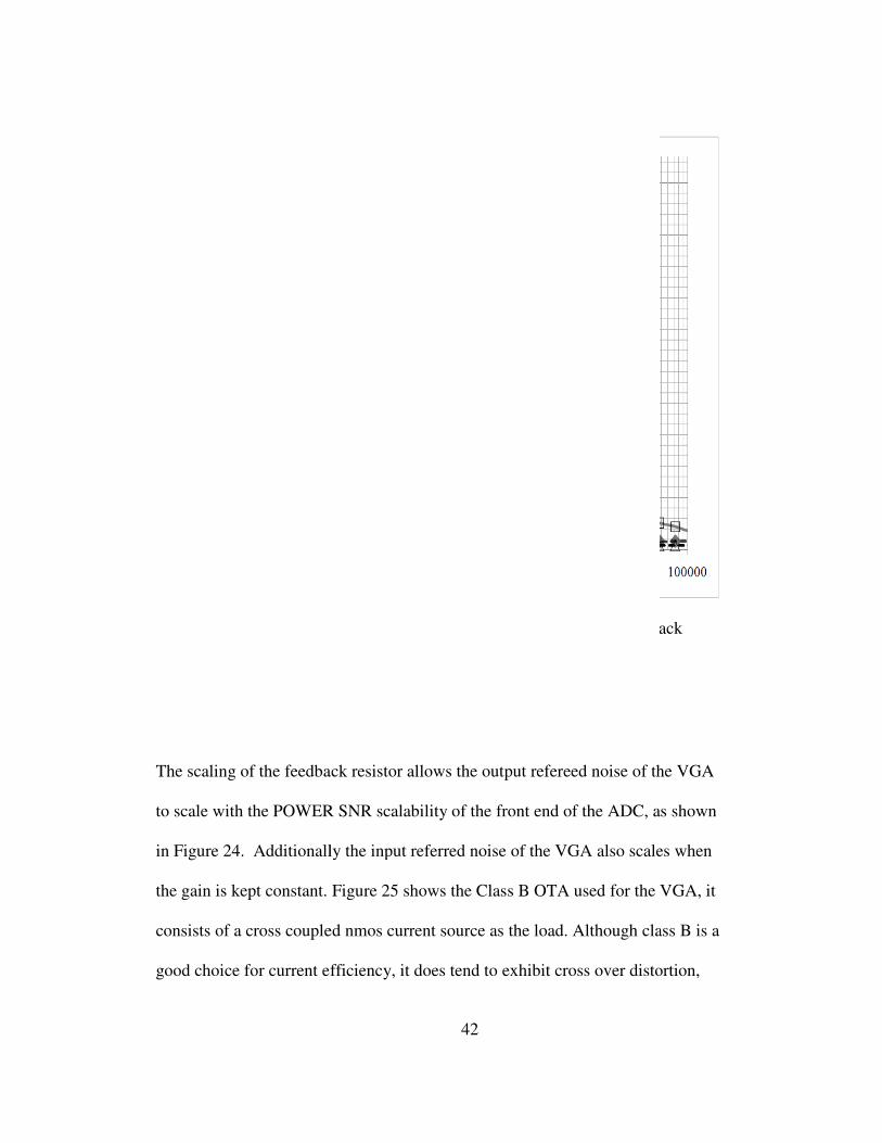
The scaling of the feedback resistor
to scale with the POWER SNR scalabil
in Figure 24. Additionally the input referred noise of the
the gain is kept constant.
consists of a cross coupled nmos current sour
good choice for current efficiency, it does tend to exhibit cross over distortion,
Figure 24. VGA output Noise Scaling for different values of the Feedback
resistor,
42
The scaling of the feedback resistor allows the output refereed noise of the VGA
to scale with the POWER SNR scalability of the front end of the ADC, as shown
. Additionally the input referred noise of the VGA also scales when
Figure 25 shows the Class B OTA used for the VGA, it
consists of a cross coupled nmos current source as the load. Although class B is a
good choice for current efficiency, it does tend to exhibit cross over distortion,
. VGA output Noise Scaling for different values of the Feedback
allows the output refereed noise of the VGA
f the ADC, as shown
VGA also scales when
B OTA used for the VGA, it
Although class B is a
good choice for current efficiency, it does tend to exhibit cross over distortion,
. VGA output Noise Scaling for different values of the Feedback
Page 55
43
which is not such a big concern for this design since the device sizes used are big
thereby minimizes the mismatch between them.
Figure 25. Class B OTA for the VGA
Page 56
44
4.3.4th
-order CT Σ∆Σ∆Σ∆Σ∆ ADC Architecture
A continuous time (CT) sigma delta has been chosen for the implementation of
the Analog to digital converter (ADC), since they are inherently lower power than
the discrete time versions due to their relaxed requirements on the OTA
bandwidths in the CT loop filters. The CT SD ADC’s intrinsic anti-aliasing has
been widely reported as one of the salient features of this architecture. In the case
of Hearing Aids this features is very helpful as it allows to band limit the input
acoustic signal to the bandwidth of the loop filter without the need of a low pass
filter. A major drawback of this approach is the sensitivity of the CT architecture
to input clock jitter. This clock jitter causes an uncertainty in the pulse width of
the clock which controls the DAC, there by modulating the charge being injected
at the input of the ADC. The return-to-zero (RZ) DAC are especially sensitivity to
jitter compared to the non-return-to-zero (NRZ) DAC due to twice the number of
clock transitions in the former.
Although multi-bit quantizer based on NRZ DAC have been shown to
reduce the SNR degradation substantially, as the number of bits of quantizer
increases other non-idealities of quantizer like DNL, INL etc may limit the
achievable SNR. Additionally power and design complexity of the quantizer also
increases with increasing number of bits, the preferred approach is to keep the
number of bits to be less than 5. This is especially true for the DAC that is
connected to the input of the loop filter, since the non-idealities of the other DACs
are attenuated by the gain of the loop filter, while the non-idealities of the first
DAC directly appear at the input of ADC causing to severely limit the achievable
Page 57
45
SNR. As such we have chosen a 1.5 Bit quantizer to be a reasonable compromise
between jitter sensitivity and design complexity. It would be shown later that this
may not have been an optimum choice as evident by the silicon results. Such
sensitivity to input clock jitter is a strong function of the number of bits in the
quantizer.
Thermal noise, DAC mismatch and other non-idealities add to the
quantization noise floor limiting the SNDR that can be realized by a CT sigma
delta. As such to achieve high resolution as required for the DHA it is necessary
to design a loop filter with more than first order noise shaping to push the
quantization down. After careful design tradeoffs b/w power and stability
requirements a 4th
order CT loop filter was chosen due to its noise shaping ability
which results in a SQNR > 100dB, in a 10 KHz BW. Such a high order loop
filter results in higher order modulator and with a 1.5 bit quantizer the stable input
range is a about 3.6dB below the full scale range of the feedback DAC.
Such a high order loop filter is usually implemented using a cascade of integrators
with wither a feed-forward summation of all the signals at input of the quantizer
or a distributed feedback architecture with signal summation happening at the
individual integrator nodes; for this thesis the later approach has been chosen.
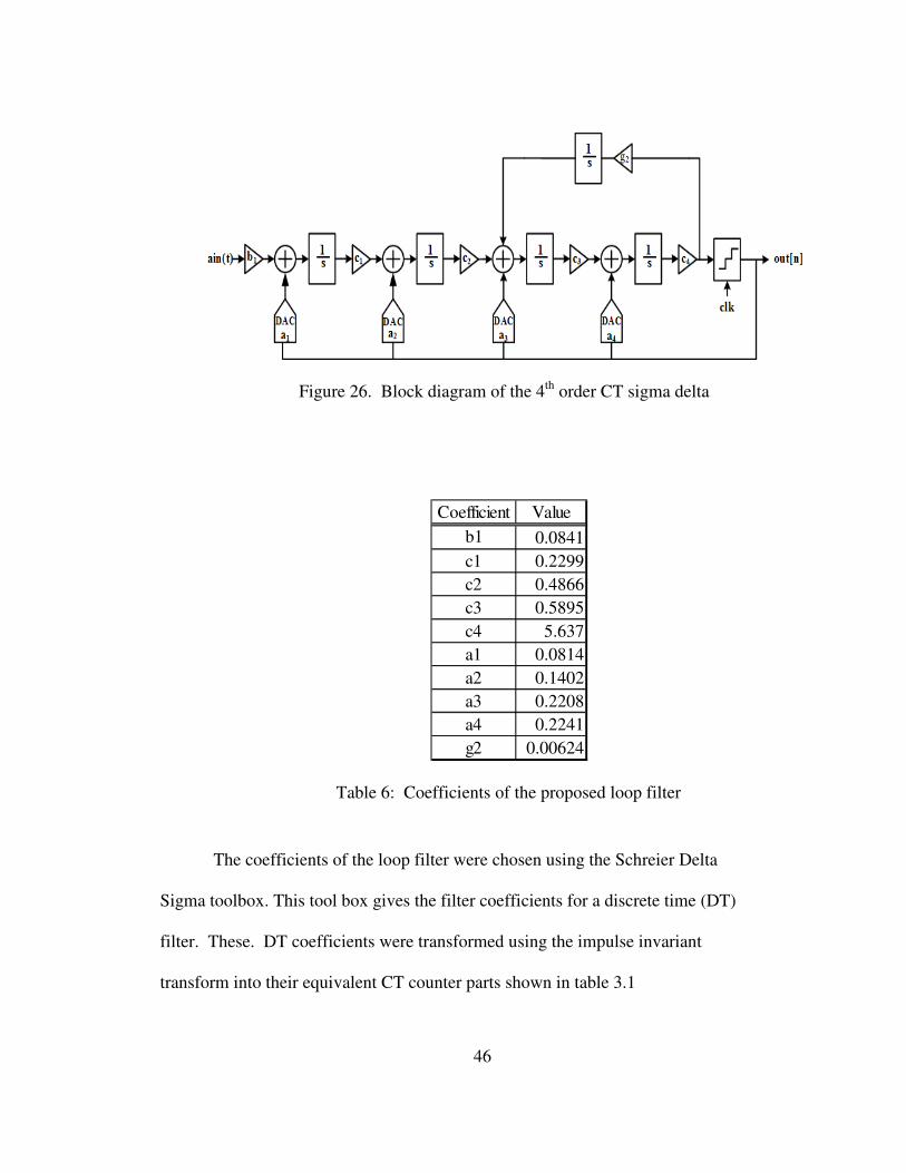
This topology consists of a cascade of 4-integrators with distributed feedback and
a local resonator as shown in Figure 20. Additionally the coefficients a1 and b1 are
kept to be equal, which ensures that the input signal is not present in any of the
integrators, the loop filter only processing the quantization noise.
Page 58
46
The coefficients of the loop filter were chosen using the Schreier Delta
Sigma toolbox. This tool box gives the filter coefficients for a discrete time (DT)
filter. These. DT coefficients were transformed using the impulse invariant
transform into their equivalent CT counter parts shown in table 3.1
Table 6: Coefficients of the proposed loop filter
Coefficient Value
b1 0.0841
c1 0.2299
c2 0.4866
c3 0.5895
c4 5.637
a1 0.0814
a2 0.1402
a3 0.2208
a4 0.2241
g2 0.00624
Figure 26. Block diagram of the 4th
order CT sigma delta
Page 59
47
4.3.1. Behavioral Model of the 4th
-order CT Σ∆Σ∆Σ∆Σ∆
Due to the inherent complexity of the CT Σ∆ architecture and its mixed signal
nature, behavioral modeling was employed for architectural tradeoff analysis. A
simulink model was used for initial coefficient sensitivity analysis, while veriloga
based model were used for more detailed analysis to study the impact of opamp
bandwidths etc. The ideal SQNR plot from the simulink model using the
coefficients given in table 4 is as shown in figure 21. A coefficient sensitivity
analysis is performed using the differential current mode veriloga model and the
simulink model. All coefficients are varied independently.
Figure 27. Power Spectral density plot of the ideal 4th
order CT Sigma Delta
Page 60
48
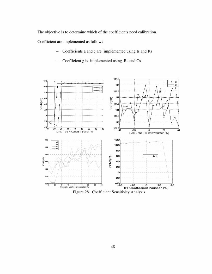
The objective is to determine which of the coefficients need calibration.
Coefficient are implemented as follows
– Coefficients a and c are implemented using Is and Rs
– Coefficient g is implemented using Rs and Cs
Figure 28. Coefficient Sensitivity Analysis
-40 -30 -20 -10 0 10 20 30 40104
106
108
110
112
114
116
Integrator Coeffecient Variation [%]
SQ
NR
(dB
)
c1
c2
c3
c4
-40 -20 0 20 40-40
-20
0
20
40
60
80
100
120
b1 Coeffecient Variation [%]
SQNR(d
B)
b1
Page 61
49
One of the primary objectives of creating a high level model of the Sigma Delta is
to be able to study the impact of the non-idealites on the SQNR of the ADC. For
the integrators the non-idealities are: primarily limited gain bandwidth, noise and
linearity, while for the feedback DACs, timing errors and unit element mismatch
are major limiters. The injection point of these non-idealities determines how they
are processed by the loop dynamics. Any non-idealities at the input stemming
from the first integrator and the first feedback DAC directly impact the SQNR of
the ADC, while the others are attenuated/filtered by the order of the preceding
stage. With this in mind in this thesis we only focused on the non-idealities of the
first integrator and first feedback DAC. No singular method was used for
modeling for these non-idealities, a combination of macro-modeling, simulink
and Matlab models were used, Figure 24, shows the macro-model. Using a circuit
based macro-model has the added advantage that it was possible to mix and match
this model with real circuit blocks, to quantify the interaction b/w the blocks.
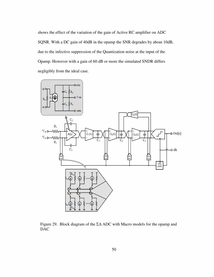
4.3.2. Amplifier Non-idealities
The finite gain and bandwidth of the Amplifier are the primary non-idealities that
limit the performance of the first active RC integrator. The Feedback DAC injects
charge at the input of the opamp, creating a perturbation of equal magnitude as
the scaled signal input, the negative feedback of the opamp acts to equalize these
and suppress the quantization noise. However the limited gain of the opamp
causes an insufficient suppression of quantization noise, which results the in-band
quantization noise floor to rise thereby reducing the SQNR of the ADC. Figure 22
Page 62
50
shows the effect of the variation of the gain of Active RC amplifier on ADC
SQNR. With a DC gain of 40dB in the opamp the SNR degrades by about 10dB,
due to the infective suppression of the Quantization noise at the input of the
Opamp. However with a gain of 60 dB or more the simulated SNDR differs
negligibly from the ideal case.
Figure 29. Block diagram of the Σ∆ ADC with Macro models for the opamp and
DAC
Page 63
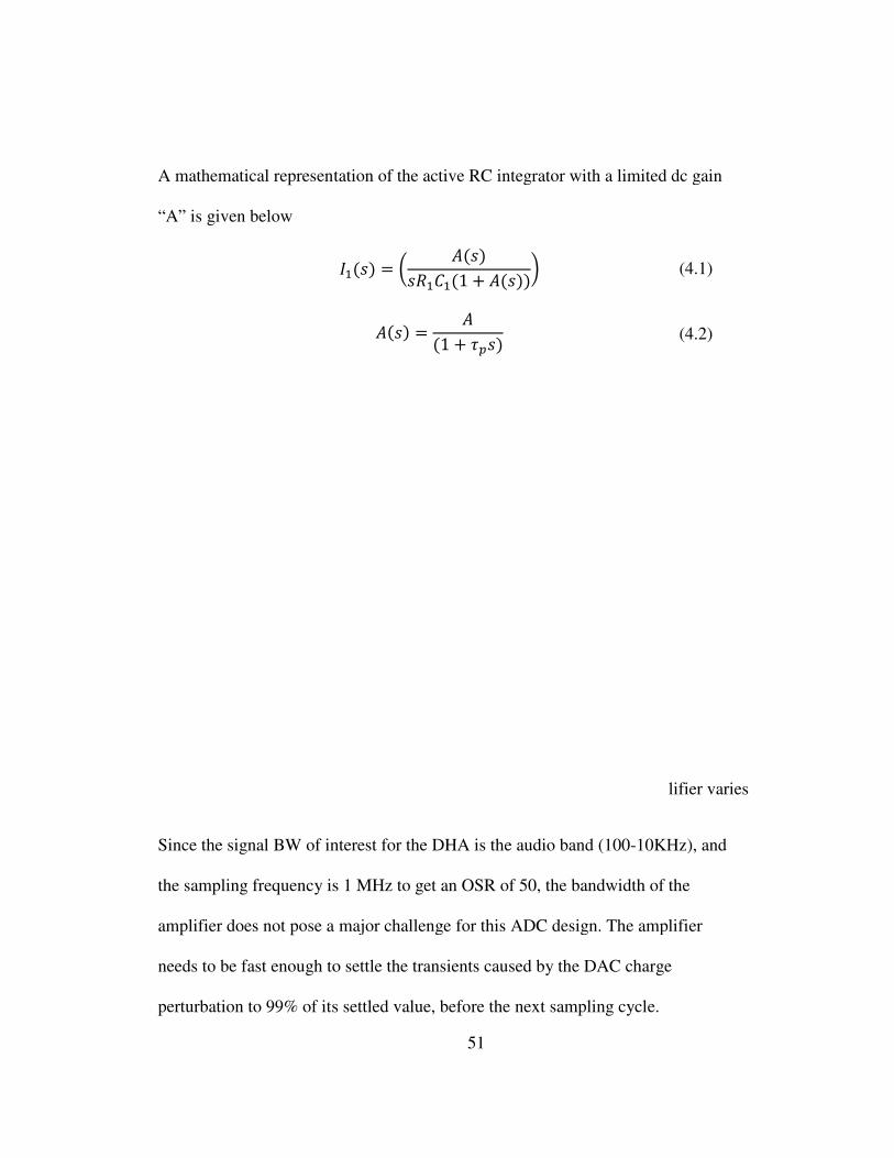
A mathematical representation of the active RC integrator with a limited dc gain
“A” is given below
Since the signal BW of in
the sampling frequency is 1 MH
amplifier does not pose a major challenge for this ADC design. The amplifier
needs to be fast enough to settle the
perturbation to 99% of its settled value
Figure 30. SQNR degradat
51
tation of the active RC integrator with a limited dc gain
S() = [ ()<S@S(1 + ())\
() = (1 + lI)
Since the signal BW of interest for the DHA is the audio band (100-10KHz
the sampling frequency is 1 MHz to get an OSR of 50, the bandwidth of the
a major challenge for this ADC design. The amplifier
needs to be fast enough to settle the transients caused by the DAC charge
% of its settled value, before the next sampling cycle.
. SQNR degradation Vs the gain of the Amp Active RC amplifier varies
tation of the active RC integrator with a limited dc gain
(4.1)
(4.2)
10KHz), and
of the
a major challenge for this ADC design. The amplifier
caused by the DAC charge
ion Vs the gain of the Amp Active RC amplifier varies
Page 64
52
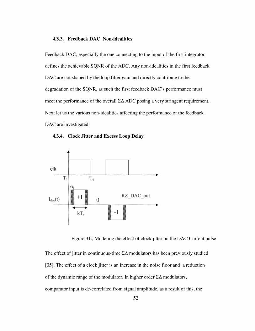
4.3.3. Feedback DAC Non-idealities
Feedback DAC, especially the one connecting to the input of the first integrator
defines the achievable SQNR of the ADC. Any non-idealities in the first feedback
DAC are not shaped by the loop filter gain and directly contribute to the
degradation of the SQNR, as such the first feedback DAC’s performance must
meet the performance of the overall Σ∆ ADC posing a very stringent requirement.
Next let us the various non-idealities affecting the performance of the feedback
DAC are investigated.
4.3.4. Clock Jitter and Excess Loop Delay
The effect of jitter in continuous-time Σ∆ modulators has been previously studied
[35]. The effect of a clock jitter is an increase in the noise floor and a reduction
of the dynamic range of the modulator. In higher order Σ∆ modulators,
comparator input is de-correlated from signal amplitude, as a result of this, the
Figure 31:, Modeling the effect of clock jitter on the DAC Current pulse
Page 65
53
jitter effect of the quantizer is negligible. On the other hand, jitter in the feedback
DAC has major effects on modulator performance [35]. Because the DAC current
is fed back to the integrators during a clock phase, uncertainty of the turn on and
turn off time of the current sources has a major effect on system performance. Fig.
29 shows that the clock jitter modulates the RZ DAC current pulse on both rising
and falling edges. The clock jitter is assumed to be white Gaussian noise with a
standard deviation of σj, affecting both rising and falling edge of the RZ DAC
current pulse as such
?&'$ = &'$mn. (4.3)
?o = 1.414 po&'$ (4.4)
Where Qj is the charge modulation that the clock jitter creates, k is the pulse high
time and Idac is the DAC current. The SNR degradation due to the clock jitter is
given by the ratio of the maximum allowable signal power divided by the jitter
noise power given as below
*]< = 10log [ m4% q*<po% .% ] (4.5)
Where fs is the sampling frequency, σj is the standard deviation of the jitter
Figure 32 shows the simulated SNR degradation due to jitter on the designed
fourth-order Σ∆ modulator. Effect on the system performance is negligible if the
clock jitter is lower than 10pS.
Page 66
54
The continuous time sigma delta loop, with emphasis on the feedback DAC, and
the clock signals used in the sigma delta modulator are shown in Fig. 30,
respectively. C1(t) is the clock for the comparator, and C2(t) is the clock for the
RZ DAC used, C3(t) is the NRZ DAC pulse. These signals are generated from a
single clock, with a non-overlapping clock generator. When C1(t) is zero, the
comparator is kept at the auto-zero phase, whereas the regenerative latch is kept at
center point. At time T1, comparator is released; the design makes sure that the
comparator sure the comparator latches before T2. From time T2 to T3 a
quantized sampled signal is fed back with the current steering DACs, where τ1
and τ2 are the turn on and turn off time of the DAC, respectively. The DAC
architecture used is a RZ architecture, where the DAC current is turned on after
the quantizer stabilizes, and is kept on for half a clock cycle. The DAC pulse
returns back to zero before the next sampling cycle. As a result of this clocking,
Figure 32:, Matlab Simulation showing the impact of jitter on the SNR of the
ADC
1,000 10,000 100,000-200
-150
-100
-50
SD
Outp
ut (d
bV
/Hz)
Frequency (Hz)
Jitter Performance
100 ps
10 ps
1 ps
Page 67
55
this DAC architecture does not show any excess loop delay. Because the loop is
closed before the next cycle, the sigma delta modulator is a cycle-to-cycle
equivalent to the discrete counterpart.
In the NRZ case, the feedback signal is turned on and off with the comparator
output. Because of the finite turn on time, τ3, and the finite turn off time, τ4, actual
current pulses are delayed from the comparator output. As a result of this delay,
the next sampling occurs before the full charge transfer, resulting in excess loop
delay. This characteristic leads to SNR degradation and higher signal distortion.
Figure 33. Clock waveforms depicting the excess loop delay impact on RZ DAC
vs NRZ DAC
Page 68
56
4.4.4th
-order CT Σ∆Σ∆Σ∆Σ∆ ADC Circuit Design
Fig 26 shows the block diagram of the implemented Σ∆ architecture, which is a
fourth-order continuous time Σ∆ modulator with a 1.5 bit quantizer (-1, 0, 1) [25].
The input stage is an active-RC integrator whereas the subsequent stages are gm-
C integrators. Furthermore, the topology uses return-to-zero current-steering
DACs in the feedback while two comparators implement the 1.5-bit flash
quantizer. In this we will discuss the design of the Quantizer and the feedback
DACs, which work in tandem
4.4.1. 4th
order CT Loop Filter Design
As shown in Fig 26, the input stage of the CT loop filter is chosen as an active RC
integrator to provide low noise and flexible interfacing with the preceding stage
VGA. While the succeeding 3 stages are implemented as gm-C integrators
providing lower
4.4.1.1.1. Input Stage Active RC integrator
Power scaling of the system is implemented at the first integrator stage of the Σ∆
modulator wherein the highest power consumption is budgeted to the first stage in
order to guarantee high SNR and linearity. Three parallel binary-scaled OTAs
implement the power/SNR scaling, which consists of 4 power consumption steps
(i.e., 8.4, 16.8, 33.6, and 67.2 W, respectively, from a 1.2-V supply). Fig. 34
shows the schematic of the unit OTA used to build the adaptive active RC
integrator. Depending on which OTAs are enabled, the input integration resistors
are scaled accordingly to increase the linearity performance (Fig. 19) At low
Page 69
57
power levels and high input sound levels, higher input resistance is used to
decrease the integration current thereby optimizing the linearity and dynamic
range of the first stage at the expense of higher input-referred noise. However, as
discussed in chapter 1, in this situation ambient noise dominates the system noise
budget, and therefore, the noise performance of the ADC can be relaxed.
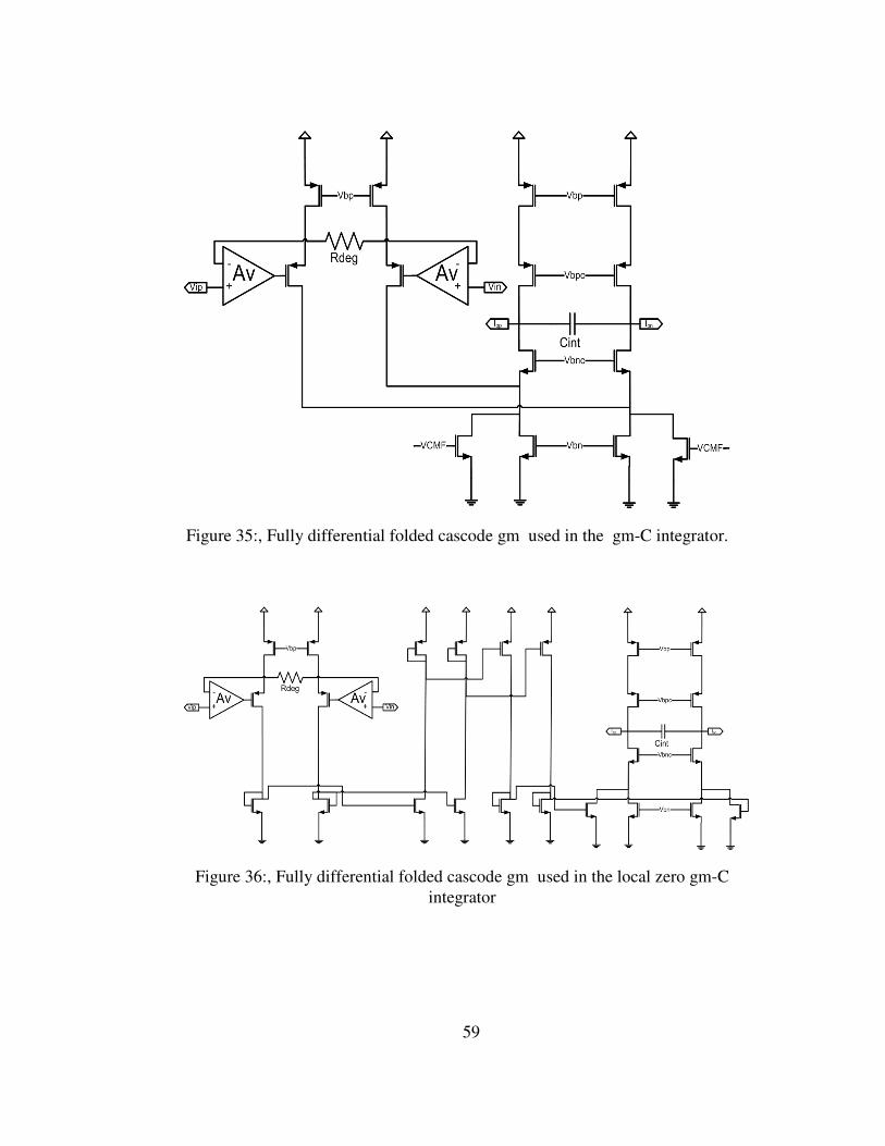
4.4.1.2.gm-C integrator
The gm stage circuit topology that has been used as the voltage to current
converter is shown in Fig. 35. A folded-cascode structure is used to maximize the
integrator DC gain. Resistive source degeneration is used to set the
transconductance value and improve linearity. Two helper amplifiers (Av)
increase the precision of the input source followers, allowing voltages Vin and Vip
to accurately appear at the degeneration resistor nodes [27]. The input differential
voltage is thus converted into a small signal current through Rdeg, which flows at
the drains of the input PMOS devices. The differential current is then applied to
the folded output stage to increase output impedance and DC gain. The gm-C
integrators have a 69-dB DC gain, a power dissipation of 9.6 µW from a 1.2 V
supply, and the integration constants are 65.9, 103.9, and 596.8 KRad/s
Page 70
58
4.4.1.3.Design gm-C integrator for the NTF Zero
In the modulator block diagram of Fig. 36, the local feedback gz block
implements a zero in the NTF just at the edge of the modulator passband, which
helps to increase the SQNR by ~20
Figure 34:, Fully differential folded cascode opamp used in the Active RC
integrator.
Page 71
59
Figure 36:, Fully differential folded cascode gm used in the local zero gm-C
integrator
Figure 35:, Fully differential folded cascode gm used in the gm-C integrator.
Page 72
60
dB [28]. Note that his NTF zero is required in order to meet the system
specifications. Because of the low frequency of the NTF zero, the required gm
value to implement the zero is at least two orders of magnitude lower than the
other gm stages.
The implemented gz transconductance stage is shown in Fig. 36. The circuit
consists of a modified version of the folded cascode transconductance stage. To
achieve a low transconductance value without increasing the size of the
degeneration resistor, the signal current of the input stage is scaled down to the
desired value in three current mirroring stages (i.e., 200:40:4:1). The gm-C
integrator has a 42 dB DC gain, with an integration constant of 500 rad/s. The
power dissipation is 5.7 µW from a 1.2-V supply
4.4.2. Quantizer Design
The schematic of the adopted three-level (1.5 bit) quantizer is shown in Fig. 37.
Return-to-Zero phase consists of a third level in the DAC. By using a three-level
quantizer, the zero state is generated as a digital code, which helps the loop
stability and increases the SQNR. The adopted comparator architecture consists of
a preamplifier and a regenerative latch [30]. The preamplifier compares the input
differential signal with the differential reference voltage. When the digital clock
signal is low, the regenerative latch is equalized, and the input signal is compared;
when the clock is high, the current differential at the output of the preamplifier
stage triggers the regenerative latch to its final value.
Page 73
61
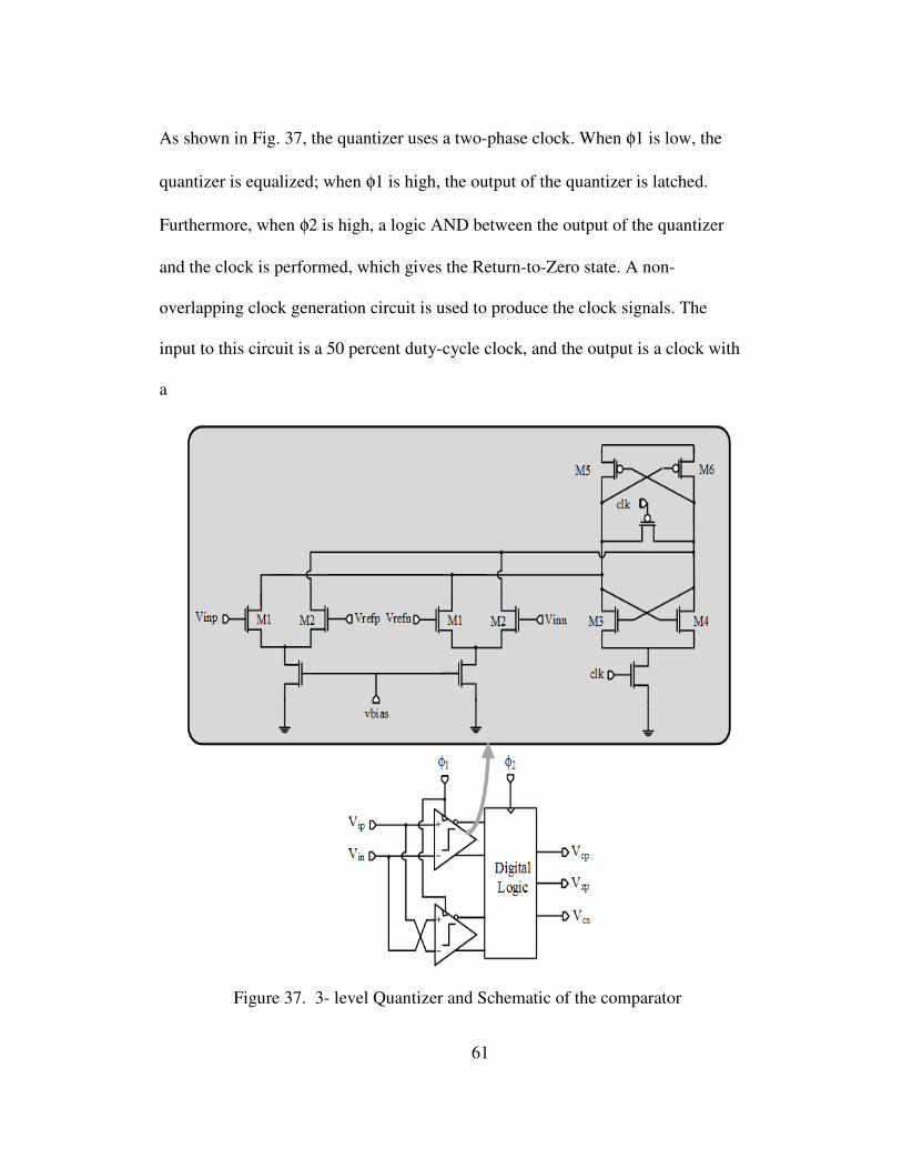
As shown in Fig. 37, the quantizer uses a two-phase clock. When φ1 is low, the
quantizer is equalized; when φ1 is high, the output of the quantizer is latched.
Furthermore, when φ2 is high, a logic AND between the output of the quantizer
and the clock is performed, which gives the Return-to-Zero state. A non-
overlapping clock generation circuit is used to produce the clock signals. The
input to this circuit is a 50 percent duty-cycle clock, and the output is a clock with
a
Figure 37. 3- level Quantizer and Schematic of the comparator
Page 74
62
larger duty cycle, which is determined by the delay of the feedback signals at
NAND gates’ inputs. The current-starved delay architecture is used to guarantee
that the rising edge of the clock (φ1) comes later than the rising edge of the
comparator enable signal (φ2) [31].
4.5.Proposed Feedback DAC Architecture
Current steering DACs are typically used in Σ∆ modulators because they enable
simple feedback mechanism to the CT loop filter, which is essentially a wired OR
connection. In our case since a complimentary current steering DAC is used
owing to the differential nature of the CT loop filter. Such a complementary DAC
Figure 38. Timing diagram of the Quantizer
Page 75
63
eases the design requirement on the common feedback loop of the opamp of the
active RC and gmC integrators of the loop filter. Figure 39 shows the high level
interconnection of the four switches and two complementary current sources used
in the
proposed feedback DAC architecture. Additionally since the first DAC is
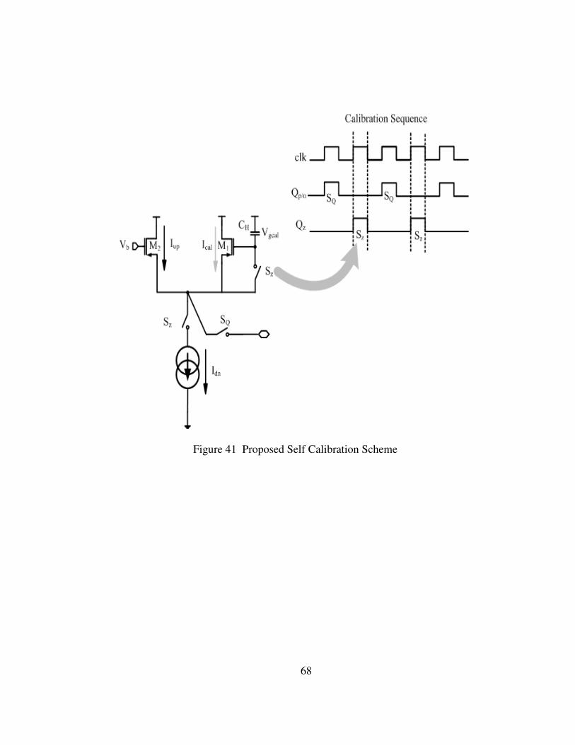
especially critical for the performance of the ADC a self calibration scheme has
been proposed.
Figure 39 A high level representation of the proposed feedback DAC
Architecture
Page 76
64
This self calibration scheme equalizes the up and down currents thereby reducing
the second order distortion caused by such a mismatch, which causes noise
folding and degradation of the SQNR/SNDR of the ADC. The Iup current
sources are implemented us PMOs while the Idn current source are implemented
using NMOS. An RZ pulse is used to control the switching of the DACs, due to
its increased tolerance to transient mismatches (ISI). The proposed RZ timing
control of the DACs is shown in the figure 38.
4.5.1. First Feedback Design and Self Calibration
The design of the feedback DAC is constrained by three major factors: current
mismatch device noise, and switching transients. These factors dictate the
achievable performance of the ADC, this is especially true for the first DAC,
since all its non-idealities appear directly at the input of the ADC without being
shaped by the gain of the loop filter. The DAC1 schematic shown in Fig. 29, has
the most stringent requirements because it is directly applied to the modulator
input nodes. In particular, DAC1 should be as linear as the whole system.
Dynamic current calibration and glitch optimization is used to overcome DAC1’s
non-idealities [33]. Moreover, current scaling is implemented for power/SNR
optimization. A bias circuit generates gate voltages for the NMOS and PMOS
current sources in the circuit. However, when the current sources are scaled up to
generate the required DAC output, the NMOS and PMOS transistors can scale
differently leading to a current mismatch. Such a mismatch not only raises the
Page 77
65
noise floor of the ADC, but could also create second harmonic distortion. In
general in CMOS process 8-10 bits of matching is achievable using proper design
and layout techniques. As such current calibration is needed to get higher than 10
bit accuracy, in our case since the quantizer is only 1.5 bits, the DAC1 non-
linearity contributes to a 2nd
order distortion for the ADC.
The current calibration principle being used shown in the figure 40 is based upon
the self calibration approach first presented by D. Wouter [34]. In calibration
mode the two S1 switches close, forcing the reference current to be equalized to
the total current flowing thru the transistors M1 and M2. Since the current thru
M2 is usually about 95-97% of the Iref, the rest of the Iref current flows through the
M1, by charging the hold Capacitor to a Vgs to support that current. In the output
mode the switch S1 is opened while the switch S2 is closed allowing the
Page 78
66
equalized current to flow out. In this scheme a reference current source and extra
spare current source is needed, which is being calibrated in the background while
the DAC operates continually without interruption. With this calibration scheme
one way correction is possible, since we are adding current, so one has to estimate
the mismatch and deliberately skew the nominal current to be less than Iref.
/TU = grHP ± trHPh + $'f (4.6)
$'f ≥ trHP (4.7)
trHP = (p8U, pk, , p8&.) (4.8)
Figure 40 Basic Self Calibration Scheme
Page 79
67
As evident from eq 3.9/3.10 the Ical has to be large enough to be able to cover for
all the source of mismatches, on the other hand a large Ical would require a large
value of gm for M1, which makes the current more sensitive to Vgs variations.
This becomes a major bottleneck for this uni-directional calibration scheme. A
differential bidirectional calibration scheme has been proposed by Razavi [35]
which circumvents some of these issues.
A unidirectional self calibration scheme is proposed in this thesis which is
shown in figure 32, which equalizes the up and down currents by having a PMOS
side calibration, to avoid the 1/f noise from affecting the ADC performance. The
up and down currents are equalized by closing the Sz switches, which forces a
current Ical, thru M2 by charging the CH capacitor to a Vgcal. By using this
scheme, an extra current source is not needed, which saves power and die area.
Additionally since the calibration is done every return-to-zero phase, there is no
additional time needed for the calibration.
.
Page 80
68
Figure 41 Proposed Self Calibration Scheme
Page 81
69
The calibration current is chosen to be about 4% less than the down
current. The value of the hold capacitor is a function of the leakage current and
the charge time, since we will calibrating every return-to-zero phase, a large value
of hold capacitor is not needed, During the calibration phase, the switches
controlled by Qzp are closed. The up current Idp and the down current Idn are
equalized while all the Qzp switches closed. The equalization is implemented by
forcing a voltage Vgcal on the hold capacitor CH to compensate for the mismatch in
the up PMOS and down NMOS devices. During normal DAC operation, Qzp
switch is open and the capacitor holds the calibrated gate voltage. Usually, in a
conventional dynamic calibration DAC, two identical DACs are designed. [33]
Figure 42. Schematic diagram of the first DAC
Page 82
70
During one clock phase, one of the DACs is calibrated and then during the
next phase, the calibrated DAC is used in the feedback. Meanwhile, the other
DAC is calibrated. The major difference between this implementation and
previous DACs is that the calibration is done during the return-to-zero phase, plus
no additional spare DAC is used.
Noise specifically flicker noise is another major limiter on the
performance. Since a cascoded DAC is used as shown figure 35, in order to
achieve the required impedance, using long devices (L >> 1 um) for the tail
device helps reduce the flicker noise. We ended up using an L= 2um an optimum
point for reducing the flicker noise and scaling the width appropriately to keep the
device saturated without making the area too big.
Figure 43. Feedback DAC input referred noise
Page 83
71
The total DAC current noise of the structure shown in Figure 35 would be a RSS
sum of the NMOS and PMOS tail devices is given below
.&'$% ≈ w83 ymn1", + z1", %k,@/e% + w83 ymn1",I + z1",I%k,@/e%
(4.9)
The DAC1 noise is the limiting factor for the performance of the ADC as
evident from figure 33 which shows the SNR of the DAC1 to be 70.5 dB at the
highest current setting. Since the cumulative noise; thermal and flicker noise of
the DAC1 tends to limit the noise floor of the ADC, the current of the DAC is
scaled to lower the thermal noise of the DAC1. The DAC1 has essentially three
Figure 44. Feedback DAC1 SNR for different current settings
Page 84
72
current settings to scale the thermal noise floor as shown in the figure 34. With
this current scaling the SNR of the DAC1 can vary from 70.5 dB to 68.8 dB.
The cumulative effect of all the non-idealities results in limiting the
performance of the CT sigma delta to around 69 dB as shown in figure 35. It
raises the thermal noise floor to by about 30 dB VS the ideal macro model based
DAC..
Figure 45. Feedback DAC input referred noise
Page 85
73
4.5.1. Other Feedback DAC Design
DAC2, DAC3 and DAC4 requirements are more relaxed than DAC1 because the
gain of each preceding integrator stage reduces the impact of the corresponding
DAC’s limitations [26]. Fig. 27 shows the implemented unity current cell of these
DACs. Dynamic current calibration is not used in this case, however; a diode-
based common-mode hold circuit is used to avoid the DAC common-mode drift.
During the zero phase, the PMOS current source and the NMOS current
source are connected to each other and because of the mismatches between the
current sources with their inherent high output impedance; the output can drift
Figure 46. Schematic diagram of the other feedback DACs (2,3 &4)
Page 86
74
either to Vdd or Vss. This results in unwanted voltage transients on the integration
nodes, once the DAC is connected to them. Such voltage transients in-turn
amplify the glitches on the current pulses raising the noise floor of the modulator.
The diode divider sets this common mode to a known voltage in less than half of a
clock period so that neither of the current sources is pushed out of saturation. The
common mode keeper settles to 0.6V in less than 0.5 us, and the current is about
4% to match the mismatch b/w the up and down currents. This scheme reduces
Figure 47. Transient simulations of the common mode keeper showing the
glitches being generated in the zero state .
Page 87
75
transient glitches, thereby improving modulator stability and the overall SQNR of
the modulator. The transient behavior of the common mode keeper is shown in
figure 38, the DAC4 has the biggest glitch on the common mode node. But since
this shaped by the gain of all the preceding stages of the CT loop filter, it has a
minimal effect on the performance of the modulator. As shown in figure 39, the
overall impact of the DAC non-linearity on the performance of the modulator is to
raise the noise floor by less than 5 dB.
Figure 48. Impact of the DAC4 nonlinearity to the performance of the
Modulator.
Page 88
76
CHAPTER 5
5. TEST SETUP AND MEASUREMENT RESULTS
A two –layer pcb board was designed to test the dual channel DHA system, the
top layer was used for signal routing mostly the bottom layer was divided in to the
islands of VSS, digital VCC and analog VCC. Special consideration was given to
the placement of the decoupling capacitors for the supplies; in fact the board
design had to be redone to ensure that the decoupling capacitors are close enough
so that the series impedance does not minimize their impact.
The test setup used to evaluate the prototype dual channel DHA is shown in the
figure 36. An analog waveform is created in Matlab and driven thru the 16-Bit
DAC in the AWG400 to the input of a low pass filter with a corner frequency of
10 kHz. An AD1838 is used for single to differential conversion to couple into
the differential signal path of the DHA system. The two bit digital output
generated the by the CT-Σ∆ modulator is sampled and stored into the memory of
the Logic Analyzers and then downloaded to a PC for post processing.
Figure 49. Test setup for measurement and evaluation of the DHA/ SD ADC
Page 89
A die photo of the fabricated
CMOS is shown in figure 20
area is 3.1 mm2.
Figure 50. Die photos of the DHA System depicting the (a) The Dual Channel
Implementation (b) Single channel details
77
fabricated prototype dual channel DHA system on a 0.25
is shown in figure 20. The active silicon area is 0.9 mm2 and the total chip
(a)
(b)
Die photos of the DHA System depicting the (a) The Dual Channel
Implementation (b) Single channel details showing the VGA, Active RC and
DACs
on a 0.25-µm
and the total chip
Die photos of the DHA System depicting the (a) The Dual Channel
showing the VGA, Active RC and
Page 90
78
Coming up with the ADC clock signal source with low enough jitter was one of
the key challenges. We used a Si time clock chip SiT8102, which has sub 1ps rms
jitter in the audio band for output frequency of 1 MHz This was to ensure that the
clock jitter is not a performance limiter for the ADC.
The die photo of the single channel is shown in figure 34 which shows the VGA,
the loop filter and the DACs/Quantizer highlighted. Each feedback DAC is placed
closed to the particular feedback point in the loop filter, while the Quantizer is
placed centrally this allows for minimal routing of the analog signals, while keeps
the delay of the quantizer signal to be equal to all the DACs.
Fig. 38 shows the measured Σ∆ modulator SNR against input amplitude. Fig. 39
shows the measured signal transfer function of the Σ∆ modulator. The measured
frequency response is flat over the 10 KHz bandwidth, and does not show any
frequency peaking. For these Si measurements the input frequency is 3.78 KHz,
the analog bandwidth is 10 KHz, and the sampling frequency is 1 MHz
The prototype ADC dissipates 106 uW from 1.2V supply, to achieve a peak SNR
of 68 dB , a 65 dB SNDR, and 60 dB THD respectively.
Page 91
79
Figure 52: Measured transfer curve of the Sigma Delta ADC showing no peaking
and channel gain flatness.
Figure 51: Measured SNR in dB Vs input Signal Amplitude.
Page 92
80
A fast fourier transform (FFT) of the ADC output with a 3.784 KHz signal -2.4
dBFS is shown in Figure 40. Fourth-order quantization noise shaping is visible in
the frequency range from 10KHz to 100KHz. The second order is clearly visible
which seems to be raising the noise floor and limiting the dynamic range of the
ADC. The Noise floor in 300 Hz to 100 KHz is increased primarily due to noise
folding and DAC thermal noise, The odd and even order distortions are artifacts
caused by the mismatches in the DAC unit element currents and switching
transients. Additionally the 2nd
order distortion has a significant in-band impact
and may also result in raising the noise floor due to noise folding.
As such Figure 54 shows that with the with the DAC Self calibration turned the
2nd
order distortion is reduced to the thermal noise floor.
Figure 53: Measured transfer curve of the Sigma Delta ADC showing no peaking
and channel gain flatness.
Page 93
81
(a)
(b)
Figure 54: Measured 2nd
order harmonic distortion of a) without calibration
enabled b) with calibration enabled.
Page 94
82
CHAPTER 6
6. CONCLUSION AND FUTURE WORKS
The measured results match the simulation results very well and clearly show that
the SNR of the ADC was limited by the thermal and flicker noise floor of the
feedback DAC. This was confirmed by simulating the SNR of the feedback DAC
which is at around 70 dB. The self calibration of the DAC up and down current
pulses worked, significantly reducing the 2nd
order harmonic distortion.
The opamp topology used in the variable gain amplifier is prone to instability;
hence it would be conducive to change that to full class AB amplifier.
The future work of this thesis would be to implement the designed Microphone
interface circuit with rest of analog front end. A multi-chip module method could
be used to connect the MEMS microphone to interface circuit. Additionally DSP
should be implemented to compensate for any gain mismatch b/w the two analog
signal chains for improved directivity. It also possible to combine the VGA
functionality with the FDDA based microphone interface circuit.
Page 95
83
REFERENCES
[1] L. M. Luxon, A. Martini, Audiological Medicine, London: Taylor & Francis
Group, 2003.
[2] M. Valente, Hearing aids: standards, options, and limitations, New York,
NY: Thieme New York, 2002.
[3] H. G. McAllister, N. D. Black, N. Waterman, “Hearing aids - a development
with digital signal processing devices” IEEE Computing & Control
Engineering Journal, vol. 6, no. 6, pp. 284-291, December 1995
[4] Neuteboom, H.; Kup, B.M.J.; Janssens, M.; , "A DSP-based hearing
instrument IC," Solid-State Circuits, IEEE Journal of , vol.32, no.11, pp.1790-
1806, Nov 1997
[5] Gata, D.G.; Sjursen, W.; Hochschild, J.R.; Fattaruso, J.W.; Fang, L.; Iannelli,
G.R.; Jiang, Z.; Branch, C.M.; Holmes, J.A.; Skorcz, M.L.; Petilli, E.M.;
Chen, S.; Wakeman, G.; Preves, D.A.; Severin, W.A.; , "A 1.1-V 270-µA
mixed-signal hearing aid chip," Solid-State Circuits, IEEE Journal of , vol.37,
no.12, pp. 1670- 1678, Dec 2002
[6] Sunyoung Kim; Jae-Youl Lee; Seong-Jun Song; Namjun Cho; Hoi-Jun Yoo; ,
"An energy-efficient analog front-end circuit for a sub-1-V digital hearing aid
chip," Solid-State Circuits, IEEE Journal of , vol.41, no.4, pp. 876- 882, April
2006
[7] P. M. Peterson, N. I. Durlach, W. M. Rabinowitz, P. M. Zurek,
“Multimicrophone adaptive beamforming for interference reduction in hearing
aids” Journal of Rehabilitation Research and Development, vol. 24 no. 4 pp.
103-110, 1987
[8] G.W. Elko, "Adaptive noise cancellation with directional microphones,"
Applications of Signal Processing to Audio and Acoustics, 1997. 1997 IEEE
ASSP Workshop on , pp.4 - 19-22, Oct 1997
[9] B. Widrow “A microphone array for hearing aids,” , IEEE Circuits and
Systems Magazine vol. , pp 26-3, 2001
[10] F. Luo , J. Yang , C. Pavlovic and A. Nehorai "Adaptive null-forming
scheme in digital hearing aids", IEEE Trans. Signal Process., vol. 50, pp.
1583, July 2002
[11] S. Je, J. Harrison, M. Kozicki, B. Bakkaloglu, S. Kiaei, and J. Chae, “In-
Situ Tuning of a MEMS Microphone Using Electrodeposited Nanostructures”,
Journal of Micromechanics and Microengineering, v.19 n.3, 035015, 2009
[12] S. Je, J. Kim, J. Harrison, M. Kozicki, and J. Chae, “In-Situ Tuning of
Omni-Directional Micro-Electro-Mechanical-Systems Microphones to
Improve Performance Fit in Hearing Aids,” Applied Physics Letters, v. 93,
123501, 2008
[13] S. Je, J. Kim, M. Kozicki, and J. Chae, “Hearing Aid Sensitivity
Optimization on Dual MEMS Microphones Using Nano-electrodeposits,”
Sensors & Transducers Journal, in-print, 2009
[14] MEMSTECH “PosiSound Series Integrated Silicon Microphone,”
accessed Oct 24th
, 2009 http://www.memstech.com/file/MULPS3CX-
Page 96
84
[15] J. Wu , G. K. Fedder and L. R. Carley "A low-noise low-offset capacitive
sensing amplifier for a 50-", IEEE J. Solid-State Circuits, vol. 39, pp. 722
2004..
[16] D. M.G., Preethichandra, and Katsunori, Shida; “A simple interface
Circuit to measure very small Capacitance changes in Capacitive Sensors,”
IEEE Trans. Instrum. Meas., vol. 50, no. 6, Dec., 2001
[17] S.-Y. Peng , M. S. Qureshi , P. E. Hasler , A. Basu and F. L. Degertekin
"A charge-based low-power high-SNR capacitive sensing interface circuit",
IEEE Trans. Circuits Syst. I, Reg. Papers, vol. 55, pp. 1863 2008.
[18] M. W. Baker and R. Sarpeshkar "A low-power high-PSRR current-mode
microphone preamplifier", IEEE J. Solid-State Circuits, vol. 38, pp. 1671
2003.
[19] M. Tavakoli and R. Sarpeshkar "An offset-canceling low-noise lock-in
architecture for capacitive sensing", IEEE J. Solid-State Circuits, vol. 38,
pp. 244 2003.
[20] E. Sackinger and W. Guggenbuhl, "A versatile building block: The
CMOS differential difference amplifier", IEEE J. Solid-State Circuits, vol.
SC-22, pp. 287 - 294, 1987
[21] S. R. Zarabadi, F. Larsen, and M. Ismail, "A reconfigurable op-
amp/DDA CMOS amplifier architecture", IEEE Trans. Circuits Syst. I, vol.
39, pp. 484 - 487, 1992
[22] J. F. Duque-Carrillo, G. Torelli, R. Perez-Aloe, J. M. Valverde, and F.
Maloberti, "Fully differential basic building blocks based on fully
differential difference amplifiers with unity-gain difference feedback", IEEE
Trans. Circuits Syst. I, vol. 42, pp. 190 - 192, 1995.
[23] C. W. Mangelsdorf "A variable gain CMOS amplifier with exponential
gain control", Symp. VLSI Circuits Dig., pp. 146 2000.
[24] J. Hauptmann , F. Dielacher , R. Steiner , C. C. Enz and F. Krummenacher
"A low-noise amplifier with automatic gain control and anticlipping control
in CMOS technology", IEEE J. Solid-State Circuits, vol. 27, pp. 974 1992.
[25] Toshio Murota, “Modified sign-magnitude DAC and method” US patent
5257027, 1993
[26] M. Ortmanns, Continuous-time sigma-delta A/D conversion:
fundamentals, performance limits and robust implementations. New York,
NY: Springer, 2006
[27] S. Pavan, Y. Tsividis, High frequency continuous time filters in didital
CMOS process, Norwell MA: Kluwer Academic Publishers Group, 2000, pp.
42-45
[28] R. Schreier, G. C. Temes, Understanding Delta Sigma Data Converters,
Piscataway, NJ: IEEE Press, 2005
[29] Shieh, J.-H.; Patil, M.; Sheu, B.J.; , "Measurement and analysis of charge
injection in MOS analog switches," Solid-State Circuits, IEEE Journal of ,
vol.22, no.2, pp. 277- 281, Apr 1987
Page 97
85
[30] Behzad Razavi, Bruce A. Wooley, “Design Techniques for High-Speed,
High-resolution Comparators”, IEEE Solid-State Circuits, IEEE Journal of,
vol. 27. no. 12, pp.1916-1926. December 1992
[31] S. H. Lewis, “Video-rate analog-to-digital conversion using pipelined
architectures” Electron. Res. Lab., Univ. California, Berkeley, Memo.
UCB/ERL M87/90, Nov. 1987, pp. 96–98.
[32] Z. Li and T. S. Fiez "A 14 bit continuous-time delta–sigma A/D modulator
with 2.5 MHz signal bandwidth", IEEE J. Solid-State Circuits, vol. 42, pp.
1873 2007
[33] S. Yan and E. Sanchez-Sinencio "A continuous-time sigma delta
modulator with 88-dB dynamic range and 1.1-MHz signal bandwidth", IEEE
J. Solid-State Circuits, vol. 39, pp. 75 2004
[34] J. A. Cherry, W. M. Snelgrove, "Excess loop delay in continuous-time
delta-sigma modulators," Circuits and Systems II: Analog and Digital Signal
Processing, IEEE Transactions on , vol.46, no.4, pp.376-389, Apr 1999